US20050173796A1 - Microelectronic assembly having array including passive elements and interconnects - Google Patents
Microelectronic assembly having array including passive elements and interconnectsDownload PDFInfo
- Publication number
- US20050173796A1 US20050173796A1US11/062,413US6241305AUS2005173796A1US 20050173796 A1US20050173796 A1US 20050173796A1US 6241305 AUS6241305 AUS 6241305AUS 2005173796 A1US2005173796 A1US 2005173796A1
- Authority
- US
- United States
- Prior art keywords
- microelectronic
- contacts
- passive
- microelectronic assembly
- conductive
- Prior art date
- Legal status (The legal status is an assumption and is not a legal conclusion. Google has not performed a legal analysis and makes no representation as to the accuracy of the status listed.)
- Granted
Links
Images


Classifications
- H—ELECTRICITY
- H01—ELECTRIC ELEMENTS
- H01L—SEMICONDUCTOR DEVICES NOT COVERED BY CLASS H10
- H01L23/00—Details of semiconductor or other solid state devices
- H01L23/48—Arrangements for conducting electric current to or from the solid state body in operation, e.g. leads, terminal arrangements ; Selection of materials therefor
- H01L23/50—Arrangements for conducting electric current to or from the solid state body in operation, e.g. leads, terminal arrangements ; Selection of materials therefor for integrated circuit devices, e.g. power bus, number of leads
- H—ELECTRICITY
- H01—ELECTRIC ELEMENTS
- H01L—SEMICONDUCTOR DEVICES NOT COVERED BY CLASS H10
- H01L23/00—Details of semiconductor or other solid state devices
- H01L23/52—Arrangements for conducting electric current within the device in operation from one component to another, i.e. interconnections, e.g. wires, lead frames
- H01L23/522—Arrangements for conducting electric current within the device in operation from one component to another, i.e. interconnections, e.g. wires, lead frames including external interconnections consisting of a multilayer structure of conductive and insulating layers inseparably formed on the semiconductor body
- H01L23/528—Layout of the interconnection structure
- H—ELECTRICITY
- H01—ELECTRIC ELEMENTS
- H01L—SEMICONDUCTOR DEVICES NOT COVERED BY CLASS H10
- H01L23/00—Details of semiconductor or other solid state devices
- H01L23/58—Structural electrical arrangements for semiconductor devices not otherwise provided for, e.g. in combination with batteries
- H01L23/64—Impedance arrangements
- H01L23/66—High-frequency adaptations
- H—ELECTRICITY
- H01—ELECTRIC ELEMENTS
- H01L—SEMICONDUCTOR DEVICES NOT COVERED BY CLASS H10
- H01L24/00—Arrangements for connecting or disconnecting semiconductor or solid-state bodies; Methods or apparatus related thereto
- H01L24/01—Means for bonding being attached to, or being formed on, the surface to be connected, e.g. chip-to-package, die-attach, "first-level" interconnects; Manufacturing methods related thereto
- H01L24/10—Bump connectors ; Manufacturing methods related thereto
- H01L24/12—Structure, shape, material or disposition of the bump connectors prior to the connecting process
- H01L24/13—Structure, shape, material or disposition of the bump connectors prior to the connecting process of an individual bump connector
- H—ELECTRICITY
- H01—ELECTRIC ELEMENTS
- H01L—SEMICONDUCTOR DEVICES NOT COVERED BY CLASS H10
- H01L24/00—Arrangements for connecting or disconnecting semiconductor or solid-state bodies; Methods or apparatus related thereto
- H01L24/01—Means for bonding being attached to, or being formed on, the surface to be connected, e.g. chip-to-package, die-attach, "first-level" interconnects; Manufacturing methods related thereto
- H01L24/10—Bump connectors ; Manufacturing methods related thereto
- H01L24/12—Structure, shape, material or disposition of the bump connectors prior to the connecting process
- H01L24/14—Structure, shape, material or disposition of the bump connectors prior to the connecting process of a plurality of bump connectors
- H—ELECTRICITY
- H01—ELECTRIC ELEMENTS
- H01L—SEMICONDUCTOR DEVICES NOT COVERED BY CLASS H10
- H01L24/00—Arrangements for connecting or disconnecting semiconductor or solid-state bodies; Methods or apparatus related thereto
- H01L24/01—Means for bonding being attached to, or being formed on, the surface to be connected, e.g. chip-to-package, die-attach, "first-level" interconnects; Manufacturing methods related thereto
- H01L24/10—Bump connectors ; Manufacturing methods related thereto
- H01L24/15—Structure, shape, material or disposition of the bump connectors after the connecting process
- H01L24/17—Structure, shape, material or disposition of the bump connectors after the connecting process of a plurality of bump connectors
- H—ELECTRICITY
- H01—ELECTRIC ELEMENTS
- H01L—SEMICONDUCTOR DEVICES NOT COVERED BY CLASS H10
- H01L24/00—Arrangements for connecting or disconnecting semiconductor or solid-state bodies; Methods or apparatus related thereto
- H01L24/73—Means for bonding being of different types provided for in two or more of groups H01L24/10, H01L24/18, H01L24/26, H01L24/34, H01L24/42, H01L24/50, H01L24/63, H01L24/71
- H—ELECTRICITY
- H01—ELECTRIC ELEMENTS
- H01L—SEMICONDUCTOR DEVICES NOT COVERED BY CLASS H10
- H01L25/00—Assemblies consisting of a plurality of semiconductor or other solid state devices
- H01L25/03—Assemblies consisting of a plurality of semiconductor or other solid state devices all the devices being of a type provided for in a single subclass of subclasses H10B, H10D, H10F, H10H, H10K or H10N, e.g. assemblies of rectifier diodes
- H01L25/04—Assemblies consisting of a plurality of semiconductor or other solid state devices all the devices being of a type provided for in a single subclass of subclasses H10B, H10D, H10F, H10H, H10K or H10N, e.g. assemblies of rectifier diodes the devices not having separate containers
- H01L25/065—Assemblies consisting of a plurality of semiconductor or other solid state devices all the devices being of a type provided for in a single subclass of subclasses H10B, H10D, H10F, H10H, H10K or H10N, e.g. assemblies of rectifier diodes the devices not having separate containers the devices being of a type provided for in group H10D89/00
- H01L25/0657—Stacked arrangements of devices
- H—ELECTRICITY
- H05—ELECTRIC TECHNIQUES NOT OTHERWISE PROVIDED FOR
- H05K—PRINTED CIRCUITS; CASINGS OR CONSTRUCTIONAL DETAILS OF ELECTRIC APPARATUS; MANUFACTURE OF ASSEMBLAGES OF ELECTRICAL COMPONENTS
- H05K1/00—Printed circuits
- H05K1/02—Details
- H05K1/0213—Electrical arrangements not otherwise provided for
- H05K1/0216—Reduction of cross-talk, noise or electromagnetic interference
- H05K1/023—Reduction of cross-talk, noise or electromagnetic interference using auxiliary mounted passive components or auxiliary substances
- H—ELECTRICITY
- H01—ELECTRIC ELEMENTS
- H01L—SEMICONDUCTOR DEVICES NOT COVERED BY CLASS H10
- H01L2224/00—Indexing scheme for arrangements for connecting or disconnecting semiconductor or solid-state bodies and methods related thereto as covered by H01L24/00
- H01L2224/01—Means for bonding being attached to, or being formed on, the surface to be connected, e.g. chip-to-package, die-attach, "first-level" interconnects; Manufacturing methods related thereto
- H01L2224/02—Bonding areas; Manufacturing methods related thereto
- H01L2224/04—Structure, shape, material or disposition of the bonding areas prior to the connecting process
- H01L2224/0401—Bonding areas specifically adapted for bump connectors, e.g. under bump metallisation [UBM]
- H—ELECTRICITY
- H01—ELECTRIC ELEMENTS
- H01L—SEMICONDUCTOR DEVICES NOT COVERED BY CLASS H10
- H01L2224/00—Indexing scheme for arrangements for connecting or disconnecting semiconductor or solid-state bodies and methods related thereto as covered by H01L24/00
- H01L2224/01—Means for bonding being attached to, or being formed on, the surface to be connected, e.g. chip-to-package, die-attach, "first-level" interconnects; Manufacturing methods related thereto
- H01L2224/02—Bonding areas; Manufacturing methods related thereto
- H01L2224/04—Structure, shape, material or disposition of the bonding areas prior to the connecting process
- H01L2224/06—Structure, shape, material or disposition of the bonding areas prior to the connecting process of a plurality of bonding areas
- H01L2224/0601—Structure
- H01L2224/0603—Bonding areas having different sizes, e.g. different heights or widths
- H—ELECTRICITY
- H01—ELECTRIC ELEMENTS
- H01L—SEMICONDUCTOR DEVICES NOT COVERED BY CLASS H10
- H01L2224/00—Indexing scheme for arrangements for connecting or disconnecting semiconductor or solid-state bodies and methods related thereto as covered by H01L24/00
- H01L2224/01—Means for bonding being attached to, or being formed on, the surface to be connected, e.g. chip-to-package, die-attach, "first-level" interconnects; Manufacturing methods related thereto
- H01L2224/02—Bonding areas; Manufacturing methods related thereto
- H01L2224/04—Structure, shape, material or disposition of the bonding areas prior to the connecting process
- H01L2224/06—Structure, shape, material or disposition of the bonding areas prior to the connecting process of a plurality of bonding areas
- H01L2224/061—Disposition
- H01L2224/0612—Layout
- H01L2224/0613—Square or rectangular array
- H01L2224/06131—Square or rectangular array being uniform, i.e. having a uniform pitch across the array
- H—ELECTRICITY
- H01—ELECTRIC ELEMENTS
- H01L—SEMICONDUCTOR DEVICES NOT COVERED BY CLASS H10
- H01L2224/00—Indexing scheme for arrangements for connecting or disconnecting semiconductor or solid-state bodies and methods related thereto as covered by H01L24/00
- H01L2224/01—Means for bonding being attached to, or being formed on, the surface to be connected, e.g. chip-to-package, die-attach, "first-level" interconnects; Manufacturing methods related thereto
- H01L2224/02—Bonding areas; Manufacturing methods related thereto
- H01L2224/04—Structure, shape, material or disposition of the bonding areas prior to the connecting process
- H01L2224/06—Structure, shape, material or disposition of the bonding areas prior to the connecting process of a plurality of bonding areas
- H01L2224/061—Disposition
- H01L2224/0612—Layout
- H01L2224/0616—Random array, i.e. array with no symmetry
- H—ELECTRICITY
- H01—ELECTRIC ELEMENTS
- H01L—SEMICONDUCTOR DEVICES NOT COVERED BY CLASS H10
- H01L2224/00—Indexing scheme for arrangements for connecting or disconnecting semiconductor or solid-state bodies and methods related thereto as covered by H01L24/00
- H01L2224/01—Means for bonding being attached to, or being formed on, the surface to be connected, e.g. chip-to-package, die-attach, "first-level" interconnects; Manufacturing methods related thereto
- H01L2224/02—Bonding areas; Manufacturing methods related thereto
- H01L2224/04—Structure, shape, material or disposition of the bonding areas prior to the connecting process
- H01L2224/06—Structure, shape, material or disposition of the bonding areas prior to the connecting process of a plurality of bonding areas
- H01L2224/065—Material
- H01L2224/06505—Bonding areas having different materials
- H—ELECTRICITY
- H01—ELECTRIC ELEMENTS
- H01L—SEMICONDUCTOR DEVICES NOT COVERED BY CLASS H10
- H01L2224/00—Indexing scheme for arrangements for connecting or disconnecting semiconductor or solid-state bodies and methods related thereto as covered by H01L24/00
- H01L2224/01—Means for bonding being attached to, or being formed on, the surface to be connected, e.g. chip-to-package, die-attach, "first-level" interconnects; Manufacturing methods related thereto
- H01L2224/10—Bump connectors; Manufacturing methods related thereto
- H01L2224/12—Structure, shape, material or disposition of the bump connectors prior to the connecting process
- H01L2224/13—Structure, shape, material or disposition of the bump connectors prior to the connecting process of an individual bump connector
- H01L2224/13001—Core members of the bump connector
- H01L2224/1301—Shape
- H01L2224/13016—Shape in side view
- H01L2224/13017—Shape in side view being non uniform along the bump connector
- H—ELECTRICITY
- H01—ELECTRIC ELEMENTS
- H01L—SEMICONDUCTOR DEVICES NOT COVERED BY CLASS H10
- H01L2224/00—Indexing scheme for arrangements for connecting or disconnecting semiconductor or solid-state bodies and methods related thereto as covered by H01L24/00
- H01L2224/01—Means for bonding being attached to, or being formed on, the surface to be connected, e.g. chip-to-package, die-attach, "first-level" interconnects; Manufacturing methods related thereto
- H01L2224/10—Bump connectors; Manufacturing methods related thereto
- H01L2224/12—Structure, shape, material or disposition of the bump connectors prior to the connecting process
- H01L2224/13—Structure, shape, material or disposition of the bump connectors prior to the connecting process of an individual bump connector
- H01L2224/13001—Core members of the bump connector
- H01L2224/13099—Material
- H—ELECTRICITY
- H01—ELECTRIC ELEMENTS
- H01L—SEMICONDUCTOR DEVICES NOT COVERED BY CLASS H10
- H01L2224/00—Indexing scheme for arrangements for connecting or disconnecting semiconductor or solid-state bodies and methods related thereto as covered by H01L24/00
- H01L2224/01—Means for bonding being attached to, or being formed on, the surface to be connected, e.g. chip-to-package, die-attach, "first-level" interconnects; Manufacturing methods related thereto
- H01L2224/10—Bump connectors; Manufacturing methods related thereto
- H01L2224/12—Structure, shape, material or disposition of the bump connectors prior to the connecting process
- H01L2224/14—Structure, shape, material or disposition of the bump connectors prior to the connecting process of a plurality of bump connectors
- H01L2224/1401—Structure
- H01L2224/1403—Bump connectors having different sizes, e.g. different diameters, heights or widths
- H—ELECTRICITY
- H01—ELECTRIC ELEMENTS
- H01L—SEMICONDUCTOR DEVICES NOT COVERED BY CLASS H10
- H01L2224/00—Indexing scheme for arrangements for connecting or disconnecting semiconductor or solid-state bodies and methods related thereto as covered by H01L24/00
- H01L2224/01—Means for bonding being attached to, or being formed on, the surface to be connected, e.g. chip-to-package, die-attach, "first-level" interconnects; Manufacturing methods related thereto
- H01L2224/10—Bump connectors; Manufacturing methods related thereto
- H01L2224/12—Structure, shape, material or disposition of the bump connectors prior to the connecting process
- H01L2224/14—Structure, shape, material or disposition of the bump connectors prior to the connecting process of a plurality of bump connectors
- H01L2224/1405—Shape
- H01L2224/14051—Bump connectors having different shapes
- H—ELECTRICITY
- H01—ELECTRIC ELEMENTS
- H01L—SEMICONDUCTOR DEVICES NOT COVERED BY CLASS H10
- H01L2224/00—Indexing scheme for arrangements for connecting or disconnecting semiconductor or solid-state bodies and methods related thereto as covered by H01L24/00
- H01L2224/01—Means for bonding being attached to, or being formed on, the surface to be connected, e.g. chip-to-package, die-attach, "first-level" interconnects; Manufacturing methods related thereto
- H01L2224/10—Bump connectors; Manufacturing methods related thereto
- H01L2224/12—Structure, shape, material or disposition of the bump connectors prior to the connecting process
- H01L2224/14—Structure, shape, material or disposition of the bump connectors prior to the connecting process of a plurality of bump connectors
- H01L2224/145—Material
- H01L2224/14505—Bump connectors having different materials
- H—ELECTRICITY
- H01—ELECTRIC ELEMENTS
- H01L—SEMICONDUCTOR DEVICES NOT COVERED BY CLASS H10
- H01L2224/00—Indexing scheme for arrangements for connecting or disconnecting semiconductor or solid-state bodies and methods related thereto as covered by H01L24/00
- H01L2224/01—Means for bonding being attached to, or being formed on, the surface to be connected, e.g. chip-to-package, die-attach, "first-level" interconnects; Manufacturing methods related thereto
- H01L2224/10—Bump connectors; Manufacturing methods related thereto
- H01L2224/15—Structure, shape, material or disposition of the bump connectors after the connecting process
- H01L2224/16—Structure, shape, material or disposition of the bump connectors after the connecting process of an individual bump connector
- H01L2224/161—Disposition
- H01L2224/16151—Disposition the bump connector connecting between a semiconductor or solid-state body and an item not being a semiconductor or solid-state body, e.g. chip-to-substrate, chip-to-passive
- H01L2224/16221—Disposition the bump connector connecting between a semiconductor or solid-state body and an item not being a semiconductor or solid-state body, e.g. chip-to-substrate, chip-to-passive the body and the item being stacked
- H01L2224/16225—Disposition the bump connector connecting between a semiconductor or solid-state body and an item not being a semiconductor or solid-state body, e.g. chip-to-substrate, chip-to-passive the body and the item being stacked the item being non-metallic, e.g. insulating substrate with or without metallisation
- H01L2224/16238—Disposition the bump connector connecting between a semiconductor or solid-state body and an item not being a semiconductor or solid-state body, e.g. chip-to-substrate, chip-to-passive the body and the item being stacked the item being non-metallic, e.g. insulating substrate with or without metallisation the bump connector connecting to a bonding area protruding from the surface of the item
- H—ELECTRICITY
- H01—ELECTRIC ELEMENTS
- H01L—SEMICONDUCTOR DEVICES NOT COVERED BY CLASS H10
- H01L2224/00—Indexing scheme for arrangements for connecting or disconnecting semiconductor or solid-state bodies and methods related thereto as covered by H01L24/00
- H01L2224/01—Means for bonding being attached to, or being formed on, the surface to be connected, e.g. chip-to-package, die-attach, "first-level" interconnects; Manufacturing methods related thereto
- H01L2224/10—Bump connectors; Manufacturing methods related thereto
- H01L2224/15—Structure, shape, material or disposition of the bump connectors after the connecting process
- H01L2224/16—Structure, shape, material or disposition of the bump connectors after the connecting process of an individual bump connector
- H01L2224/161—Disposition
- H01L2224/16151—Disposition the bump connector connecting between a semiconductor or solid-state body and an item not being a semiconductor or solid-state body, e.g. chip-to-substrate, chip-to-passive
- H01L2224/16221—Disposition the bump connector connecting between a semiconductor or solid-state body and an item not being a semiconductor or solid-state body, e.g. chip-to-substrate, chip-to-passive the body and the item being stacked
- H01L2224/16265—Disposition the bump connector connecting between a semiconductor or solid-state body and an item not being a semiconductor or solid-state body, e.g. chip-to-substrate, chip-to-passive the body and the item being stacked the item being a discrete passive component
- H—ELECTRICITY
- H01—ELECTRIC ELEMENTS
- H01L—SEMICONDUCTOR DEVICES NOT COVERED BY CLASS H10
- H01L2224/00—Indexing scheme for arrangements for connecting or disconnecting semiconductor or solid-state bodies and methods related thereto as covered by H01L24/00
- H01L2224/01—Means for bonding being attached to, or being formed on, the surface to be connected, e.g. chip-to-package, die-attach, "first-level" interconnects; Manufacturing methods related thereto
- H01L2224/10—Bump connectors; Manufacturing methods related thereto
- H01L2224/15—Structure, shape, material or disposition of the bump connectors after the connecting process
- H01L2224/17—Structure, shape, material or disposition of the bump connectors after the connecting process of a plurality of bump connectors
- H01L2224/171—Disposition
- H—ELECTRICITY
- H01—ELECTRIC ELEMENTS
- H01L—SEMICONDUCTOR DEVICES NOT COVERED BY CLASS H10
- H01L2224/00—Indexing scheme for arrangements for connecting or disconnecting semiconductor or solid-state bodies and methods related thereto as covered by H01L24/00
- H01L2224/01—Means for bonding being attached to, or being formed on, the surface to be connected, e.g. chip-to-package, die-attach, "first-level" interconnects; Manufacturing methods related thereto
- H01L2224/42—Wire connectors; Manufacturing methods related thereto
- H01L2224/47—Structure, shape, material or disposition of the wire connectors after the connecting process
- H01L2224/48—Structure, shape, material or disposition of the wire connectors after the connecting process of an individual wire connector
- H01L2224/481—Disposition
- H01L2224/48151—Connecting between a semiconductor or solid-state body and an item not being a semiconductor or solid-state body, e.g. chip-to-substrate, chip-to-passive
- H01L2224/48221—Connecting between a semiconductor or solid-state body and an item not being a semiconductor or solid-state body, e.g. chip-to-substrate, chip-to-passive the body and the item being stacked
- H01L2224/48225—Connecting between a semiconductor or solid-state body and an item not being a semiconductor or solid-state body, e.g. chip-to-substrate, chip-to-passive the body and the item being stacked the item being non-metallic, e.g. insulating substrate with or without metallisation
- H01L2224/4824—Connecting between the body and an opposite side of the item with respect to the body
- H—ELECTRICITY
- H01—ELECTRIC ELEMENTS
- H01L—SEMICONDUCTOR DEVICES NOT COVERED BY CLASS H10
- H01L2224/00—Indexing scheme for arrangements for connecting or disconnecting semiconductor or solid-state bodies and methods related thereto as covered by H01L24/00
- H01L2224/74—Apparatus for manufacturing arrangements for connecting or disconnecting semiconductor or solid-state bodies and for methods related thereto
- H01L2224/78—Apparatus for connecting with wire connectors
- H01L2224/7825—Means for applying energy, e.g. heating means
- H01L2224/783—Means for applying energy, e.g. heating means by means of pressure
- H01L2224/78301—Capillary
- H—ELECTRICITY
- H01—ELECTRIC ELEMENTS
- H01L—SEMICONDUCTOR DEVICES NOT COVERED BY CLASS H10
- H01L2225/00—Details relating to assemblies covered by the group H01L25/00 but not provided for in its subgroups
- H01L2225/03—All the devices being of a type provided for in the same main group of the same subclass of class H10, e.g. assemblies of rectifier diodes
- H01L2225/04—All the devices being of a type provided for in the same main group of the same subclass of class H10, e.g. assemblies of rectifier diodes the devices not having separate containers
- H01L2225/065—All the devices being of a type provided for in the same main group of the same subclass of class H10
- H01L2225/06503—Stacked arrangements of devices
- H01L2225/0651—Wire or wire-like electrical connections from device to substrate
- H—ELECTRICITY
- H01—ELECTRIC ELEMENTS
- H01L—SEMICONDUCTOR DEVICES NOT COVERED BY CLASS H10
- H01L2225/00—Details relating to assemblies covered by the group H01L25/00 but not provided for in its subgroups
- H01L2225/03—All the devices being of a type provided for in the same main group of the same subclass of class H10, e.g. assemblies of rectifier diodes
- H01L2225/04—All the devices being of a type provided for in the same main group of the same subclass of class H10, e.g. assemblies of rectifier diodes the devices not having separate containers
- H01L2225/065—All the devices being of a type provided for in the same main group of the same subclass of class H10
- H01L2225/06503—Stacked arrangements of devices
- H01L2225/0652—Bump or bump-like direct electrical connections from substrate to substrate
- H—ELECTRICITY
- H01—ELECTRIC ELEMENTS
- H01L—SEMICONDUCTOR DEVICES NOT COVERED BY CLASS H10
- H01L2225/00—Details relating to assemblies covered by the group H01L25/00 but not provided for in its subgroups
- H01L2225/03—All the devices being of a type provided for in the same main group of the same subclass of class H10, e.g. assemblies of rectifier diodes
- H01L2225/04—All the devices being of a type provided for in the same main group of the same subclass of class H10, e.g. assemblies of rectifier diodes the devices not having separate containers
- H01L2225/065—All the devices being of a type provided for in the same main group of the same subclass of class H10
- H01L2225/06503—Stacked arrangements of devices
- H01L2225/06527—Special adaptation of electrical connections, e.g. rewiring, engineering changes, pressure contacts, layout
- H—ELECTRICITY
- H01—ELECTRIC ELEMENTS
- H01L—SEMICONDUCTOR DEVICES NOT COVERED BY CLASS H10
- H01L2225/00—Details relating to assemblies covered by the group H01L25/00 but not provided for in its subgroups
- H01L2225/03—All the devices being of a type provided for in the same main group of the same subclass of class H10, e.g. assemblies of rectifier diodes
- H01L2225/04—All the devices being of a type provided for in the same main group of the same subclass of class H10, e.g. assemblies of rectifier diodes the devices not having separate containers
- H01L2225/065—All the devices being of a type provided for in the same main group of the same subclass of class H10
- H01L2225/06503—Stacked arrangements of devices
- H01L2225/06541—Conductive via connections through the device, e.g. vertical interconnects, through silicon via [TSV]
- H—ELECTRICITY
- H01—ELECTRIC ELEMENTS
- H01L—SEMICONDUCTOR DEVICES NOT COVERED BY CLASS H10
- H01L2225/00—Details relating to assemblies covered by the group H01L25/00 but not provided for in its subgroups
- H01L2225/03—All the devices being of a type provided for in the same main group of the same subclass of class H10, e.g. assemblies of rectifier diodes
- H01L2225/04—All the devices being of a type provided for in the same main group of the same subclass of class H10, e.g. assemblies of rectifier diodes the devices not having separate containers
- H01L2225/065—All the devices being of a type provided for in the same main group of the same subclass of class H10
- H01L2225/06503—Stacked arrangements of devices
- H01L2225/06572—Auxiliary carrier between devices, the carrier having an electrical connection structure
- H—ELECTRICITY
- H01—ELECTRIC ELEMENTS
- H01L—SEMICONDUCTOR DEVICES NOT COVERED BY CLASS H10
- H01L2225/00—Details relating to assemblies covered by the group H01L25/00 but not provided for in its subgroups
- H01L2225/03—All the devices being of a type provided for in the same main group of the same subclass of class H10, e.g. assemblies of rectifier diodes
- H01L2225/04—All the devices being of a type provided for in the same main group of the same subclass of class H10, e.g. assemblies of rectifier diodes the devices not having separate containers
- H01L2225/065—All the devices being of a type provided for in the same main group of the same subclass of class H10
- H01L2225/06503—Stacked arrangements of devices
- H01L2225/06582—Housing for the assembly, e.g. chip scale package [CSP]
- H01L2225/06586—Housing with external bump or bump-like connectors
- H—ELECTRICITY
- H01—ELECTRIC ELEMENTS
- H01L—SEMICONDUCTOR DEVICES NOT COVERED BY CLASS H10
- H01L24/00—Arrangements for connecting or disconnecting semiconductor or solid-state bodies; Methods or apparatus related thereto
- H01L24/01—Means for bonding being attached to, or being formed on, the surface to be connected, e.g. chip-to-package, die-attach, "first-level" interconnects; Manufacturing methods related thereto
- H01L24/42—Wire connectors; Manufacturing methods related thereto
- H01L24/47—Structure, shape, material or disposition of the wire connectors after the connecting process
- H01L24/48—Structure, shape, material or disposition of the wire connectors after the connecting process of an individual wire connector
- H—ELECTRICITY
- H01—ELECTRIC ELEMENTS
- H01L—SEMICONDUCTOR DEVICES NOT COVERED BY CLASS H10
- H01L2924/00—Indexing scheme for arrangements or methods for connecting or disconnecting semiconductor or solid-state bodies as covered by H01L24/00
- H01L2924/0001—Technical content checked by a classifier
- H01L2924/00013—Fully indexed content
- H—ELECTRICITY
- H01—ELECTRIC ELEMENTS
- H01L—SEMICONDUCTOR DEVICES NOT COVERED BY CLASS H10
- H01L2924/00—Indexing scheme for arrangements or methods for connecting or disconnecting semiconductor or solid-state bodies as covered by H01L24/00
- H01L2924/0001—Technical content checked by a classifier
- H01L2924/00014—Technical content checked by a classifier the subject-matter covered by the group, the symbol of which is combined with the symbol of this group, being disclosed without further technical details
- H—ELECTRICITY
- H01—ELECTRIC ELEMENTS
- H01L—SEMICONDUCTOR DEVICES NOT COVERED BY CLASS H10
- H01L2924/00—Indexing scheme for arrangements or methods for connecting or disconnecting semiconductor or solid-state bodies as covered by H01L24/00
- H01L2924/01—Chemical elements
- H01L2924/01005—Boron [B]
- H—ELECTRICITY
- H01—ELECTRIC ELEMENTS
- H01L—SEMICONDUCTOR DEVICES NOT COVERED BY CLASS H10
- H01L2924/00—Indexing scheme for arrangements or methods for connecting or disconnecting semiconductor or solid-state bodies as covered by H01L24/00
- H01L2924/01—Chemical elements
- H01L2924/01013—Aluminum [Al]
- H—ELECTRICITY
- H01—ELECTRIC ELEMENTS
- H01L—SEMICONDUCTOR DEVICES NOT COVERED BY CLASS H10
- H01L2924/00—Indexing scheme for arrangements or methods for connecting or disconnecting semiconductor or solid-state bodies as covered by H01L24/00
- H01L2924/01—Chemical elements
- H01L2924/01019—Potassium [K]
- H—ELECTRICITY
- H01—ELECTRIC ELEMENTS
- H01L—SEMICONDUCTOR DEVICES NOT COVERED BY CLASS H10
- H01L2924/00—Indexing scheme for arrangements or methods for connecting or disconnecting semiconductor or solid-state bodies as covered by H01L24/00
- H01L2924/01—Chemical elements
- H01L2924/01027—Cobalt [Co]
- H—ELECTRICITY
- H01—ELECTRIC ELEMENTS
- H01L—SEMICONDUCTOR DEVICES NOT COVERED BY CLASS H10
- H01L2924/00—Indexing scheme for arrangements or methods for connecting or disconnecting semiconductor or solid-state bodies as covered by H01L24/00
- H01L2924/01—Chemical elements
- H01L2924/01029—Copper [Cu]
- H—ELECTRICITY
- H01—ELECTRIC ELEMENTS
- H01L—SEMICONDUCTOR DEVICES NOT COVERED BY CLASS H10
- H01L2924/00—Indexing scheme for arrangements or methods for connecting or disconnecting semiconductor or solid-state bodies as covered by H01L24/00
- H01L2924/01—Chemical elements
- H01L2924/01033—Arsenic [As]
- H—ELECTRICITY
- H01—ELECTRIC ELEMENTS
- H01L—SEMICONDUCTOR DEVICES NOT COVERED BY CLASS H10
- H01L2924/00—Indexing scheme for arrangements or methods for connecting or disconnecting semiconductor or solid-state bodies as covered by H01L24/00
- H01L2924/01—Chemical elements
- H01L2924/01042—Molybdenum [Mo]
- H—ELECTRICITY
- H01—ELECTRIC ELEMENTS
- H01L—SEMICONDUCTOR DEVICES NOT COVERED BY CLASS H10
- H01L2924/00—Indexing scheme for arrangements or methods for connecting or disconnecting semiconductor or solid-state bodies as covered by H01L24/00
- H01L2924/01—Chemical elements
- H01L2924/01078—Platinum [Pt]
- H—ELECTRICITY
- H01—ELECTRIC ELEMENTS
- H01L—SEMICONDUCTOR DEVICES NOT COVERED BY CLASS H10
- H01L2924/00—Indexing scheme for arrangements or methods for connecting or disconnecting semiconductor or solid-state bodies as covered by H01L24/00
- H01L2924/01—Chemical elements
- H01L2924/01079—Gold [Au]
- H—ELECTRICITY
- H01—ELECTRIC ELEMENTS
- H01L—SEMICONDUCTOR DEVICES NOT COVERED BY CLASS H10
- H01L2924/00—Indexing scheme for arrangements or methods for connecting or disconnecting semiconductor or solid-state bodies as covered by H01L24/00
- H01L2924/01—Chemical elements
- H01L2924/01087—Francium [Fr]
- H—ELECTRICITY
- H01—ELECTRIC ELEMENTS
- H01L—SEMICONDUCTOR DEVICES NOT COVERED BY CLASS H10
- H01L2924/00—Indexing scheme for arrangements or methods for connecting or disconnecting semiconductor or solid-state bodies as covered by H01L24/00
- H01L2924/013—Alloys
- H01L2924/0132—Binary Alloys
- H01L2924/01322—Eutectic Alloys, i.e. obtained by a liquid transforming into two solid phases
- H—ELECTRICITY
- H01—ELECTRIC ELEMENTS
- H01L—SEMICONDUCTOR DEVICES NOT COVERED BY CLASS H10
- H01L2924/00—Indexing scheme for arrangements or methods for connecting or disconnecting semiconductor or solid-state bodies as covered by H01L24/00
- H01L2924/013—Alloys
- H01L2924/014—Solder alloys
- H—ELECTRICITY
- H01—ELECTRIC ELEMENTS
- H01L—SEMICONDUCTOR DEVICES NOT COVERED BY CLASS H10
- H01L2924/00—Indexing scheme for arrangements or methods for connecting or disconnecting semiconductor or solid-state bodies as covered by H01L24/00
- H01L2924/10—Details of semiconductor or other solid state devices to be connected
- H01L2924/11—Device type
- H01L2924/14—Integrated circuits
- H01L2924/143—Digital devices
- H01L2924/1433—Application-specific integrated circuit [ASIC]
- H—ELECTRICITY
- H01—ELECTRIC ELEMENTS
- H01L—SEMICONDUCTOR DEVICES NOT COVERED BY CLASS H10
- H01L2924/00—Indexing scheme for arrangements or methods for connecting or disconnecting semiconductor or solid-state bodies as covered by H01L24/00
- H01L2924/15—Details of package parts other than the semiconductor or other solid state devices to be connected
- H01L2924/151—Die mounting substrate
- H01L2924/156—Material
- H01L2924/15786—Material with a principal constituent of the material being a non metallic, non metalloid inorganic material
- H01L2924/15787—Ceramics, e.g. crystalline carbides, nitrides or oxides
- H—ELECTRICITY
- H01—ELECTRIC ELEMENTS
- H01L—SEMICONDUCTOR DEVICES NOT COVERED BY CLASS H10
- H01L2924/00—Indexing scheme for arrangements or methods for connecting or disconnecting semiconductor or solid-state bodies as covered by H01L24/00
- H01L2924/19—Details of hybrid assemblies other than the semiconductor or other solid state devices to be connected
- H01L2924/1901—Structure
- H01L2924/1904—Component type
- H01L2924/19041—Component type being a capacitor
- H—ELECTRICITY
- H01—ELECTRIC ELEMENTS
- H01L—SEMICONDUCTOR DEVICES NOT COVERED BY CLASS H10
- H01L2924/00—Indexing scheme for arrangements or methods for connecting or disconnecting semiconductor or solid-state bodies as covered by H01L24/00
- H01L2924/19—Details of hybrid assemblies other than the semiconductor or other solid state devices to be connected
- H01L2924/1901—Structure
- H01L2924/1904—Component type
- H01L2924/19042—Component type being an inductor
- H—ELECTRICITY
- H01—ELECTRIC ELEMENTS
- H01L—SEMICONDUCTOR DEVICES NOT COVERED BY CLASS H10
- H01L2924/00—Indexing scheme for arrangements or methods for connecting or disconnecting semiconductor or solid-state bodies as covered by H01L24/00
- H01L2924/19—Details of hybrid assemblies other than the semiconductor or other solid state devices to be connected
- H01L2924/1901—Structure
- H01L2924/1904—Component type
- H01L2924/19043—Component type being a resistor
- H—ELECTRICITY
- H01—ELECTRIC ELEMENTS
- H01L—SEMICONDUCTOR DEVICES NOT COVERED BY CLASS H10
- H01L2924/00—Indexing scheme for arrangements or methods for connecting or disconnecting semiconductor or solid-state bodies as covered by H01L24/00
- H01L2924/19—Details of hybrid assemblies other than the semiconductor or other solid state devices to be connected
- H01L2924/191—Disposition
- H01L2924/19101—Disposition of discrete passive components
- H01L2924/19102—Disposition of discrete passive components in a stacked assembly with the semiconductor or solid state device
- H01L2924/19103—Disposition of discrete passive components in a stacked assembly with the semiconductor or solid state device interposed between the semiconductor or solid-state device and the die mounting substrate, i.e. chip-on-passive
- H—ELECTRICITY
- H01—ELECTRIC ELEMENTS
- H01L—SEMICONDUCTOR DEVICES NOT COVERED BY CLASS H10
- H01L2924/00—Indexing scheme for arrangements or methods for connecting or disconnecting semiconductor or solid-state bodies as covered by H01L24/00
- H01L2924/30—Technical effects
- H01L2924/301—Electrical effects
- H01L2924/30105—Capacitance
- H—ELECTRICITY
- H01—ELECTRIC ELEMENTS
- H01L—SEMICONDUCTOR DEVICES NOT COVERED BY CLASS H10
- H01L2924/00—Indexing scheme for arrangements or methods for connecting or disconnecting semiconductor or solid-state bodies as covered by H01L24/00
- H01L2924/30—Technical effects
- H01L2924/301—Electrical effects
- H01L2924/30107—Inductance
- H—ELECTRICITY
- H01—ELECTRIC ELEMENTS
- H01L—SEMICONDUCTOR DEVICES NOT COVERED BY CLASS H10
- H01L2924/00—Indexing scheme for arrangements or methods for connecting or disconnecting semiconductor or solid-state bodies as covered by H01L24/00
- H01L2924/30—Technical effects
- H01L2924/301—Electrical effects
- H01L2924/3011—Impedance
- H—ELECTRICITY
- H01—ELECTRIC ELEMENTS
- H01L—SEMICONDUCTOR DEVICES NOT COVERED BY CLASS H10
- H01L2924/00—Indexing scheme for arrangements or methods for connecting or disconnecting semiconductor or solid-state bodies as covered by H01L24/00
- H01L2924/30—Technical effects
- H01L2924/301—Electrical effects
- H01L2924/3025—Electromagnetic shielding
- H—ELECTRICITY
- H05—ELECTRIC TECHNIQUES NOT OTHERWISE PROVIDED FOR
- H05K—PRINTED CIRCUITS; CASINGS OR CONSTRUCTIONAL DETAILS OF ELECTRIC APPARATUS; MANUFACTURE OF ASSEMBLAGES OF ELECTRICAL COMPONENTS
- H05K2201/00—Indexing scheme relating to printed circuits covered by H05K1/00
- H05K2201/10—Details of components or other objects attached to or integrated in a printed circuit board
- H05K2201/10431—Details of mounted components
- H05K2201/10507—Involving several components
- H05K2201/10515—Stacked components
- H—ELECTRICITY
- H05—ELECTRIC TECHNIQUES NOT OTHERWISE PROVIDED FOR
- H05K—PRINTED CIRCUITS; CASINGS OR CONSTRUCTIONAL DETAILS OF ELECTRIC APPARATUS; MANUFACTURE OF ASSEMBLAGES OF ELECTRICAL COMPONENTS
- H05K2201/00—Indexing scheme relating to printed circuits covered by H05K1/00
- H05K2201/10—Details of components or other objects attached to or integrated in a printed circuit board
- H05K2201/10431—Details of mounted components
- H05K2201/10507—Involving several components
- H05K2201/1053—Mounted components directly electrically connected to each other, i.e. not via the PCB
- H—ELECTRICITY
- H05—ELECTRIC TECHNIQUES NOT OTHERWISE PROVIDED FOR
- H05K—PRINTED CIRCUITS; CASINGS OR CONSTRUCTIONAL DETAILS OF ELECTRIC APPARATUS; MANUFACTURE OF ASSEMBLAGES OF ELECTRICAL COMPONENTS
- H05K2201/00—Indexing scheme relating to printed circuits covered by H05K1/00
- H05K2201/10—Details of components or other objects attached to or integrated in a printed circuit board
- H05K2201/10613—Details of electrical connections of non-printed components, e.g. special leads
- H05K2201/10621—Components characterised by their electrical contacts
- H05K2201/10636—Leadless chip, e.g. chip capacitor or resistor
- H—ELECTRICITY
- H05—ELECTRIC TECHNIQUES NOT OTHERWISE PROVIDED FOR
- H05K—PRINTED CIRCUITS; CASINGS OR CONSTRUCTIONAL DETAILS OF ELECTRIC APPARATUS; MANUFACTURE OF ASSEMBLAGES OF ELECTRICAL COMPONENTS
- H05K2201/00—Indexing scheme relating to printed circuits covered by H05K1/00
- H05K2201/10—Details of components or other objects attached to or integrated in a printed circuit board
- H05K2201/10613—Details of electrical connections of non-printed components, e.g. special leads
- H05K2201/10621—Components characterised by their electrical contacts
- H05K2201/10674—Flip chip
- Y—GENERAL TAGGING OF NEW TECHNOLOGICAL DEVELOPMENTS; GENERAL TAGGING OF CROSS-SECTIONAL TECHNOLOGIES SPANNING OVER SEVERAL SECTIONS OF THE IPC; TECHNICAL SUBJECTS COVERED BY FORMER USPC CROSS-REFERENCE ART COLLECTIONS [XRACs] AND DIGESTS
- Y02—TECHNOLOGIES OR APPLICATIONS FOR MITIGATION OR ADAPTATION AGAINST CLIMATE CHANGE
- Y02P—CLIMATE CHANGE MITIGATION TECHNOLOGIES IN THE PRODUCTION OR PROCESSING OF GOODS
- Y02P70/00—Climate change mitigation technologies in the production process for final industrial or consumer products
- Y02P70/50—Manufacturing or production processes characterised by the final manufactured product
Definitions
- the present applicationrelates to microelectronic assemblies and, in particular, to packages incorporating passive elements, especially discrete resistive and/or capacitive elements, as well as to stacked packages, and to components and methods useful in making such assemblies.
- passive elementscan sometimes be incorporated within semiconductor chips, they are usually limited to very small value devices, due to the relatively large amounts of the chip device area that they tend to occupy. Larger value devices can only be provided external to the chip. Therefore, in the aforementioned memory and communication devices, many of the required passive devices must be provided off of the chip. Indeed, some chips require hundreds of such passive elements per package.
- a microelectronic assemblywhich includes a microelectronic element such as a chip or element of a package.
- a plurality of surface-mountable contactsare arranged in an array exposed at a major surface of the microelectronic element.
- One or more passive elementse.g., a resistor, inductor, capacitor, or combination of the same are mounted to the microelectronic element, with an inner terminal of the passive element conductively mounted to an exposed surface of one contact and an outer terminal displaced vertically from the major surface of the microelectronic element.
- the microelectronic assemblyis bonded to a further microelectronic element, e.g., another chip, package element, or circuit panel, which faces the first microelectronic element, with the passive elements being disposed in series between contacts of the first and second microelectronic elements.
- a further microelectronic elemente.g., another chip, package element, or circuit panel, which faces the first microelectronic element, with the passive elements being disposed in series between contacts of the first and second microelectronic elements.
- passive elementsare mounted in series between a contact of one microelectronic element, e.g., a package element, and a contact of another microelectronic element such as a circuit panel.
- Various joining techniquescan be used, such as hierarchical joining, in which an attach temperature of a bonding medium used to bond the passive elements to the first microelectronic element is higher than an attach temperature of a bonding medium used to make soldered connections between the two microelectronic elements.
- passive elementsare arranged at desired locations maintained within a sheet-like or tape-like dielectric element and the dielectric element is aligned and held in place to a microelectronic element such as a chip or package element.
- Solder ballscan then be provided into openings in the dielectric element, and the assembly is then heated to join the passive elements to the microelectronic element and to form conductive bumps at locations of the solder balls.
- itcan either be left in place in the microelectronic assembly, or be removed, such as by etching performed selective to the material at the surface of the microelectronic element.
- FIG. 1is a perspective view of a microelectronic assembly in accordance with one embodiment of the invention.
- FIG. 2is an enlarged partial, perspective view of the microelectronic assembly in accordance with the embodiment of the invention illustrated in FIG. 1 .
- FIG. 3is a top (plan) view of the microelectronic assembly in accordance with the embodiment illustrated in FIG. 1 .
- FIG. 4is a partial elevational view of the microelectronic assembly in accordance with the embodiment illustrated in FIG. 1 .
- FIG. 5is a top (plan) view of an element of a microelectronic assembly in accordance with another embodiment of the invention.
- FIG. 6is an elevational view of a microelectronic assembly in accordance with one embodiment of the invention.
- FIG. 6Ais a top plan view of a dielectric element utilized in a method of fabricating a microelectronic assembly in accordance with one embodiment of the invention.
- FIG. 7is a diagrammatic sectional view of a stacked package in accordance with another embodiment of the invention.
- FIG. 8is a fragmentary diagrammatic sectional view of a stacked package in accordance with another embodiment of the invention.
- FIG. 9is an elevational view of a portion of an assembly in accordance another embodiment of the invention.
- a microelectronic assemblyin which a microelectronic element, e.g., a chip or element of a package has a plurality of contacts exposed at a major surface.
- the microelectronic elementis a chip, in which the contacts are bond pads of the chip. Some of the bond pads of the chip are bonded by a conductive medium, e.g., a solder, to contacts of a package element such as a chip carrier or substrate, for example. Others of the bond pads have series connections through passive elements, especially resistive and/or capacitive elements to the contacts of the package element.
- small passive elementse.g., discrete passives can be located in very close proximity to individual input/output (“IO”) pads of the chip, such as for impedance matching purposes, among others.
- IOinput/output
- a microelectronic assembly or packageincludes a chip having a plurality of bond pads arranged in an array at a major surface of the chip.
- a package elementhas a corresponding array of contacts arranged at a surface opposing the major surface of the chip. Some of the bond pads of the array of the chip are bonded to the contacts of the package element via solder bumps.
- Discrete passive elementsbeing, in one embodiment, either individual discrete resistors, individual discrete capacitors, or both, are mounted to others of the bond pads, the discrete passive elements having inner terminals conductively mounted to the bond pads.
- the discrete passive elementsalso have outer terminals which are insulated from the inner terminals, such that as mounted, the outer terminals are displaced, e.g., in a vertical direction, from the major surface of the chip.
- the inner and outer terminalsare connected to each other through one or more passive components, e.g., a resistor and/or a capacitor.
- the passive elementincludes a discrete capacitor
- one plate of the discrete capacitorcan be conductively connected to the inner terminal while the other plate of the discrete capacitor is connected to the outer terminal.
- the outer terminalsare mounted to ones of a corresponding array of contacts exposed at the surface of the package element. In such way, series connections are provided through the discrete passive elements between the chip and the package element.
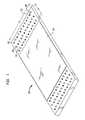
- FIG. 1is a perspective view of a microelectronic element viewed toward a contact-bearing surface 102 on which a plurality of contacts 104 , 106 are provided, e.g., as arranged in an array.
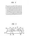
- FIG. 2is an enlarged view of the same microelectronic element 100 , showing individual contacts 104 , 106 of the microelectronic element 100 in greater detail.
- the microelectronic element 100 shown in FIG. 1can be a semiconductor chip on which active devices and/or circuits 110 are provided.
- the microelectronic elementis a package element, e.g., chip carrier, which may be part of a packaged chip.
- the contactsi.e., the bond pads of the chip, are arranged in an M by N array having a number M of the contacts aligned in a first lateral direction extending along the surface 102 of the chip and a number N of contacts aligned in a second lateral direction extending along the surface 102 of the chip 100 .
- the numbers M and Ncan each be equal to or greater than one, and can vary independently from one another.
- the number “M” of contacts disposed in a direction of the width of the chipis nine, and the number “N” of contacts disposed in a direction of the length of the chip is three.
- the contactscan be disposed as a single row of contacts.
- the contacts of the arrayare provided at a fine or relatively fine pitch, e.g., having a pitch of a few mils (thousandths of one inch), up to a few tens of mils between centers of adjacent ones of the contacts.
- Measurements provided in standard unitsare illustrative, and not limiting, as the size of such features are the same whether stated in standard or metric units.
- Discrete passive elementsare available having dimensions comparable to solder balls considered to be medium-sized at this time. Specifically, some discrete passive elements can be made which have rectilinear box-shape, have dimensions of 0.6 mm ⁇ 0.3 mm ⁇ 0.3 mm. These dimensions translate to approximately 24 mils ⁇ 12 mils ⁇ 12 mils.
- the passive elementoccupies a volume which is not substantially greater than a volume occupied by a conductive bump, e.g., solder bump disposed on a contact of the microelectronic element.
- a height of the passive elementis not greater than a height of conductive bumps of the package.
- the contacts of the arrayare disposed at a uniform pitch in each direction of the array.
- the contactscan be arranged to have different pitches in the different lateral directions in which the contacts are aligned within the array.
- the pitch between adjacent contacts of the arraycan be uniform in both lateral directions (length, width along the surface) at 0.8 mm pitch or perhaps 1.0 mm pitch in both lateral directions.
- the pitchcould be 0.8 mm in one lateral direction and be a different pitch, such as 1.2 mm or 2.0 mm or other measurement in the other lateral direction.
- the contacts of the arrayi.e., the bond pads 104 , 106 of the chip
- the contacts of the arrayare disposed at a uniform pitch, i.e., being the same pitch in each of the two orthogonal directions (width and length) of the chip, and the numbers M and N of bond pads that are aligned in each of the width and length directions are each greater than one.
- Passive elements 107e.g., elements incorporating passive components such as resistors, capacitors or inductors, are bonded to some bond pads 106 of the array of bond pads through a fusible conductive medium such as a solder, tin, or eutectic composition, for example.
- Solder bumps 105are bonded to other bond pads 104 of the chip.
- the passive elementsare disposed at alternating locations in a checkerboard pattern throughout the M by N array of contacts, such that the solder balls occupy some locations of the array, and passive elements occupy every location.
- passive elementsare disposed at locations within the array determined according to particular requirements of the chip, and hence, do not exhibit a pattern which is regular and uniform to the eye.
- the passive elementsinclude inner terminals 112 and outer terminals 114 , in form of conductive, e.g., metallic end caps which are insulated from each other.
- the inner terminals 112provide conductive connection to the chip 100 through bond pads 106
- outer terminals 114are available to provide conductive connection to another microelectronic element, such as a package element.
- a bonding medium 120preferably, a fusible conductive medium such as a solder, bonds the inner terminals to the bond pads 106 . In the arrangement shown in FIG. 4 , such bonding medium 120 can be referred to as an inner conductive bump.
- Solder bumps 105disposed at other bond pads 104 of the array of contacts, facilitate the formation of conductive interconnects between the chip 100 and a package element 200 ( FIG. 5 ) to be mounted to the chip 100 .
- the chipis suitable for mounting to the package element using a flip-chip mounting technique.
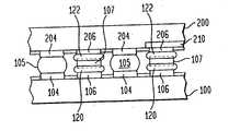
- a flip-chip mounting techniqueas illustrated in FIG. 6 , a chip 100 is placed with the contact-bearing surface 102 facing a corresponding mounting surface of the package element 200 , e.g., chip carrier or substrate, and bond pads 104 of the chip are bonded to corresponding contacts 204 of the package element 200 via solder bumps 105 .
- the passive elements 107are mounted between the bond pads 106 of the chip and corresponding contacts 206 of the package element. As shown in FIG. 6 , the passive elements may be conductively connected to the chip and the package element through masses of solder or other conductive bonding medium referred to herein as inner conductive bumps 120 and outer conductive bumps 122 , respectively.
- such microelectronic element 200may include conductive patterns, e.g., conductive planes 210 , 220 which extend laterally along the major surface 202 of the package element.
- the conductive planesare used to maintain fixed potentials at locations extending across the package element, to which some of the bond pads 104 of the chip 100 ( FIG. 5 ) are conductively connected through solder bumps 105 , and to which some bond pads 106 of the chip may be connected through passive elements 122 .
- One of the conductive planescan be a ground plane, for example, and one of the conductive planes can be maintained at a voltage other than ground.
- the microelectronic element 100can be an element of a package to be mounted to a chip, or can be an external element to be mounted to a circuit panel.
- a package elementcan be articles such as commonly referred to as a chip carrier, e.g., a dielectric sheet or tape having a patterned metal layer.
- the microelectronic elementis a connecting element of a package, e.g., a chip carrier, or other package element or connecting element which conductively connects a chip to another interconnect element such as a circuit panel, as described and shown in commonly owned U.S. patent application Ser. Nos. 10/746,810 filed Dec. 24, 2003; Ser. No. 10/783,314 filed Feb. 20, 2004, or U.S. Pat. No. 6,856,007, all of said applications and said patent being hereby incorporated herein by reference.
- the microelectronic elementcan be a substrate having inorganic and/or organic components, e.g., a ceramic substrate.
- the package element 100( FIGS. 1-4 ) is a chip carrier in which the contacts on the side of the chip carrier facing the chip can be arranged in an array having a pitch and placement that coincides with a pitch of the bond pads of a chip.
- the second microelectronic element 200can be a circuit panel, being illustratively, an epoxy-resin or FR-4 type circuit board, to which a corresponding package element is mounted, with the passive elements joined in series connections between contacts of the circuit panel and corresponding contacts of the package element.
- a methodwill now be described for fabricating microelectronic assemblies in accordance with the foregoing embodiments.
- a common feature of the microelectronic assemblies shown in FIGS. 1-4 and 6is the mounting of passive elements at locations within an array of contacts that are interspersed among high conductivity interconnects that vertically connect one microelectronic element such as a chip to another such as a package element.
- the passive elementsmust be mounted to locations in the array of contacts in a way that is compatible with the way that high conductivity interconnects are formed.
- the microelectronic assembly shown in the partial elevational view of FIG. 6is fabricated as follows.
- the microelectronic assemblyincludes two microelectronic elements, e.g., a chip and a package element, or a package element and another interconnection element, the two microelectronic elements having contacts on surfaces which face each other when the two microelectronic elements are assembled together.
- a microelectronic element 100( FIG. 4 ) is provided which includes a plurality of contacts, e.g., contacts of a package element, conductive terminals of a circuit panel, or bond pads of a chip which are exposed at a major surface of the microelectronic element.
- passive elements 307having at least first terminals (e.g., end caps 112 ; FIG. 4 ) coated in a solder or other fusible conductive medium are embedded at desired positions in a dielectric element 300 , e.g., a tape or interposer element.
- the passive elementshave first terminals on one side of the dielectric material and second terminals on the opposite side of the dielectric material from the first terminals.
- the dielectric materialpreferably includes an organic material such as a solder mask, or may include an inorganic material or combination of organic and inorganic materials.
- the dielectric element 300may be constructed of a material which is to remain permanently within the package.
- dielectric material of the dielectric elementis removable by an etchant that otherwise does not harm the exposed major surface of the microelectronic element.
- the dielectric element 300has openings 310 sized to accommodate solder balls in places where conductive contacts are to be made.
- the passive elementsare provided in a regular recurring pattern, and the openings for the solder balls are also provided in a regular recurring pattern, to facilitate ease of fabrication and better usability for different microelectronic elements.
- the passive elements and the solder ballscan be arrayed in a checkerboard pattern such as that shown and described above with reference to FIGS. 1-4 .
- the dielectric element 300 carrying the passive elementsis aligned to one microelectronic element and is then held together to the microelectronic element.
- Solder ballscan then be provided within the openings of the dielectric element, e.g., as through a process of passing solder balls through a screen aligned to the openings.
- Heatingis then applied to surface mount, i.e., join the solder-coated first terminals at one end of each passive element to the contacts exposed at the surface of the microelectronic element and to melt the solder balls to form solder bumps on other contacts exposed at the surface of the microelectronic element. This forms a microelectronic assembly similar to that shown and described above relative to FIGS.
- the dielectric materialis preferably one that has low permittivity, i.e., having a low dielectric constant K in order to avoid undesirable parasitic capacitance between interconnects.
- the dielectric materialpreferably also has a coefficient of thermal expansion close to that of a chip and/or has a low modulus of elasticity, such as is characteristic of many organic materials.
- the low modulus of elasticity of organic materialshelps the organic material to mitigate the effects of differential strain which occurs between a chip and another microelectronic element such as a chip carrier, due to CTE mismatch.
- an etchantis used to remove the dielectric material after initially joining first terminals of the passive elements to the first microelectronic element, or after joining the second, opposite terminals of the passive elements to the other microelectronic element to form the assembly including both microelectronic elements. This can be done, since the dielectric element is no longer needed to hold the passive elements and solder bumps in place.
- microelectronic assemblies in accordance with this inventioncan be performed by any suitable method.
- passive elements on which terminals are coated with solderi.e., “solder-tipped” elements
- solder-tipped elementsare first positioned on contacts of one microelectronic element, e.g., a circuit panel, and then joined thereto in a heating step.
- solder ballsare positioned on another microelectronic element, e.g., an external contact-bearing surface of a package, and then joined to the package by heating to form solder bumps.
- the circuit panel with the passive elements joined theretois aligned to the package having the solder bumps and the aligned elements are heated to join the free ends of the bumps and the terminals to the contacts of the corresponding microelectronic elements to form the microelectronic assembly.
- the foregoing techniqueis applied to fabricate a package having passive elements and solder bumps disposed within the interfacial region between a chip and a package element.
- a hierarchical joining methodcan be used.
- the passive elementsare first joined to one microelectronic element, using a solder or other fusible conductive medium which has a relatively high attach temperature.
- Subsequent joining processesare then performed using a solder or fusible conductive medium which has a lower attach temperature than the first solder or fusible conductive medium, such that the conductive medium that holds the first terminals of the passive elements to the first microelectronic element continues to hold the passive elements in place during later joining processes.
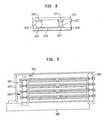
- FIG. 7another embodiment of the invention is shown.
- passive componentsare used as vertical conductors in place of one, or more, solder balls for coupling units of a stacked assembly together.
- the stacked assembly of FIG. 7is similar to the other stacks described above and, e.g., includes a number of circuit panels 1486 arranged in a vertical stack and coupled to each other via conductive elements as represented by solder balls 1483 .
- the stacked assemblyincludes one, or more, passive components, coupled between these circuit panels. This is illustratively shown in FIG. 7 by passive components 1401 , 1402 , 1403 , 1404 and 1405 .
- each passive componentis small enough to span the gap 1495 between adjacent circuit panels.
- a passive componentsuch as a resistor, capacitor, inductor or the like 1401 may have a small housing 1420 with metallic end caps 1421 at its top and bottom ends.
- the end capsmay be connected to the corresponding terminals 1423 of two adjacent units in the stack by a bonding material such as solder which coats the end caps but which does not bridge between the end caps and hence does not short-circuit the passive element within the housing.
- the passive elementsmay be pre-coated with the bonding material so that they can be applied in manner similar to solder balls.
- the exterior of housing 1420may have a polymeric or other surface which is not wettable by the bonding material and hence resists bridging by the bonding material.
- a passive element 1471 connectedmay be connected between a first terminal 1472 of a first unit 1477 in the stack and a first terminal 1473 of an adjacent second unit 1478 .
- the first terminal of the second unitin turn may be connected by a trace 1479 on the second unit to a second terminal 1474 of the second unit, which in turn is connected by a solder ball 1475 to a second terminal 1476 of the first unit.
- solder ball 1475may be replaced by a further passive element (not shown) so that two passive elements are connected in series in the internal circuit of the first unit 1477 .
- a passive element 1451is connected between a signal-carrying terminal 1452 of the topmost operative unit of the stack circuit and a metallic shield 1453 overlying the top of the stack.
- Shield 1453has a side wall 1454 extending vertically to the bottom of the stack.
- the passive componentis thus connected between the top of a vertical signal bus 1455 and a ground potential applied through the shield.
- passive component 1451serves as a terminating element.
- passive component 1452may be a simple resistor to provide a pull-down termination at the top of the signal bus.
- one or more vertical ground busesare connected by conductive elements such as solder balls 1483 to the shield. This arrangement illustrates that the ground or power connections of termination elements to the circuit board can be made by connections other than the vertical buses of the stacked assembly.
Landscapes
- Engineering & Computer Science (AREA)
- Microelectronics & Electronic Packaging (AREA)
- Power Engineering (AREA)
- Computer Hardware Design (AREA)
- Physics & Mathematics (AREA)
- Condensed Matter Physics & Semiconductors (AREA)
- General Physics & Mathematics (AREA)
- Electromagnetism (AREA)
- Geometry (AREA)
- Semiconductor Integrated Circuits (AREA)
Abstract
Description
- This application is a continuation-in-part of U.S. patent application Ser. No. 10/454,029 filed Jun. 4, 2003. Said application is a continuation-in-part of U.S. patent application Ser. No. 10/267,450, filed Oct. 9, 2002, which in turn claims benefit of U.S. Provisional Patent Application Ser. No. 60/328,038 filed Oct. 9, 2001. The disclosures of all the afore-mentioned applications are hereby incorporated by reference herein.
- The present application relates to microelectronic assemblies and, in particular, to packages incorporating passive elements, especially discrete resistive and/or capacitive elements, as well as to stacked packages, and to components and methods useful in making such assemblies.
- Many types of semiconductor chips contain integrated circuits which require passive elements, e.g., discrete resistive, capacitive and/or inductive devices to be mounted in close proximity to input/output pads of the chip and other pads, for purposes such as impedance matching, i.e., termination of a transmission line, DC (direct current) blocking, decoupling, or other purposes. This is especially true of integrated circuits for memory devices, and communication devices, e.g., especially high-speed serial communication interfaces and radio communication devices.
- While passive elements can sometimes be incorporated within semiconductor chips, they are usually limited to very small value devices, due to the relatively large amounts of the chip device area that they tend to occupy. Larger value devices can only be provided external to the chip. Therefore, in the aforementioned memory and communication devices, many of the required passive devices must be provided off of the chip. Indeed, some chips require hundreds of such passive elements per package.
- The need for external passive elements poses difficulties to the design and fabrication of a microelectronic assembly such as the chip package and higher order assemblies. A large number of passive elements is difficult to incorporate onto a circuit panel to be mounted to the package. It also becomes very difficult to route wiring traces on a circuit board between all of the required passive elements and the signal I/O of the chip. In addition, superior performance can sometimes be achieved when the passive element and the I/O pad of the chip are disposed in close proximity. Accordingly, it would be desirable to provide a way of mounting passive elements in a package which addresses these and other concerns.
- According to one aspect of the invention, a microelectronic assembly is provided which includes a microelectronic element such as a chip or element of a package. A plurality of surface-mountable contacts are arranged in an array exposed at a major surface of the microelectronic element. One or more passive elements, e.g., a resistor, inductor, capacitor, or combination of the same are mounted to the microelectronic element, with an inner terminal of the passive element conductively mounted to an exposed surface of one contact and an outer terminal displaced vertically from the major surface of the microelectronic element.
- In a preferred embodiment of the invention, the microelectronic assembly is bonded to a further microelectronic element, e.g., another chip, package element, or circuit panel, which faces the first microelectronic element, with the passive elements being disposed in series between contacts of the first and second microelectronic elements.
- In a method of fabricating a microelectronic assembly, passive elements are mounted in series between a contact of one microelectronic element, e.g., a package element, and a contact of another microelectronic element such as a circuit panel. Various joining techniques can be used, such as hierarchical joining, in which an attach temperature of a bonding medium used to bond the passive elements to the first microelectronic element is higher than an attach temperature of a bonding medium used to make soldered connections between the two microelectronic elements. In a particular embodiment, passive elements are arranged at desired locations maintained within a sheet-like or tape-like dielectric element and the dielectric element is aligned and held in place to a microelectronic element such as a chip or package element. Solder balls can then be provided into openings in the dielectric element, and the assembly is then heated to join the passive elements to the microelectronic element and to form conductive bumps at locations of the solder balls. Depending upon the material used to form the dielectric element, it can either be left in place in the microelectronic assembly, or be removed, such as by etching performed selective to the material at the surface of the microelectronic element.
FIG. 1 is a perspective view of a microelectronic assembly in accordance with one embodiment of the invention.FIG. 2 is an enlarged partial, perspective view of the microelectronic assembly in accordance with the embodiment of the invention illustrated inFIG. 1 .FIG. 3 is a top (plan) view of the microelectronic assembly in accordance with the embodiment illustrated inFIG. 1 .FIG. 4 is a partial elevational view of the microelectronic assembly in accordance with the embodiment illustrated inFIG. 1 .FIG. 5 is a top (plan) view of an element of a microelectronic assembly in accordance with another embodiment of the invention.FIG. 6 is an elevational view of a microelectronic assembly in accordance with one embodiment of the invention.FIG. 6A is a top plan view of a dielectric element utilized in a method of fabricating a microelectronic assembly in accordance with one embodiment of the invention.FIG. 7 is a diagrammatic sectional view of a stacked package in accordance with another embodiment of the invention.FIG. 8 is a fragmentary diagrammatic sectional view of a stacked package in accordance with another embodiment of the invention.FIG. 9 is an elevational view of a portion of an assembly in accordance another embodiment of the invention.- In accordance with embodiments of the invention described herein, a microelectronic assembly is provided in which a microelectronic element, e.g., a chip or element of a package has a plurality of contacts exposed at a major surface. In one embodiment, the microelectronic element is a chip, in which the contacts are bond pads of the chip. Some of the bond pads of the chip are bonded by a conductive medium, e.g., a solder, to contacts of a package element such as a chip carrier or substrate, for example. Others of the bond pads have series connections through passive elements, especially resistive and/or capacitive elements to the contacts of the package element. In such way, small passive elements, e.g., discrete passives can be located in very close proximity to individual input/output (“IO”) pads of the chip, such as for impedance matching purposes, among others. By mounting passive elements to contacts within the interfacial spacing between a circuit panel and a package, or between a package element and a chip, the aforementioned problems of mounting passive elements on an external surface of a circuit panel can be avoided.
- Moreover, such placement of the passive elements within an array of contacts reclaims area on the circuit panel that would otherwise be taken up by passive elements outside the array area, as well as the area required for wiring to and from the passive elements.
- In a particular embodiment, a microelectronic assembly or package includes a chip having a plurality of bond pads arranged in an array at a major surface of the chip. A package element has a corresponding array of contacts arranged at a surface opposing the major surface of the chip. Some of the bond pads of the array of the chip are bonded to the contacts of the package element via solder bumps. Discrete passive elements, being, in one embodiment, either individual discrete resistors, individual discrete capacitors, or both, are mounted to others of the bond pads, the discrete passive elements having inner terminals conductively mounted to the bond pads. The discrete passive elements also have outer terminals which are insulated from the inner terminals, such that as mounted, the outer terminals are displaced, e.g., in a vertical direction, from the major surface of the chip. The inner and outer terminals are connected to each other through one or more passive components, e.g., a resistor and/or a capacitor. For example, when the passive element includes a discrete capacitor, one plate of the discrete capacitor can be conductively connected to the inner terminal while the other plate of the discrete capacitor is connected to the outer terminal. The outer terminals, in turn, are mounted to ones of a corresponding array of contacts exposed at the surface of the package element. In such way, series connections are provided through the discrete passive elements between the chip and the package element.
FIG. 1 is a perspective view of a microelectronic element viewed toward a contact-bearingsurface 102 on which a plurality ofcontacts FIG. 2 is an enlarged view of the samemicroelectronic element 100, showingindividual contacts microelectronic element 100 in greater detail.- In one embodiment, the
microelectronic element 100 shown inFIG. 1 can be a semiconductor chip on which active devices and/orcircuits 110 are provided. In another embodiment, described below, the microelectronic element is a package element, e.g., chip carrier, which may be part of a packaged chip. In the example shown inFIG. 1 , the contacts, i.e., the bond pads of the chip, are arranged in an M by N array having a number M of the contacts aligned in a first lateral direction extending along thesurface 102 of the chip and a number N of contacts aligned in a second lateral direction extending along thesurface 102 of thechip 100. The numbers M and N can each be equal to or greater than one, and can vary independently from one another. In the example shown inFIG. 1 , the number “M” of contacts disposed in a direction of the width of the chip is nine, and the number “N” of contacts disposed in a direction of the length of the chip is three. - In another example (not shown), the contacts can be disposed as a single row of contacts. Stated another way, in one such example, the contacts are disposed in a single row extending in a direction of the width of the chip, e.g., the array measures M=5 (five) contacts in a widthwise direction, and N=1 (one) contact in the lengthwise direction. In yet another example, the contacts can be disposed as a single row of contacts in the direction of the length of the chip, e.g., the array measures M=1 (one) contact in the widthwise direction, and N=10 (ten) contacts in the lengthwise direction.
- In one preferred embodiment, the contacts of the array are provided at a fine or relatively fine pitch, e.g., having a pitch of a few mils (thousandths of one inch), up to a few tens of mils between centers of adjacent ones of the contacts. Measurements provided in standard units are illustrative, and not limiting, as the size of such features are the same whether stated in standard or metric units. Discrete passive elements are available having dimensions comparable to solder balls considered to be medium-sized at this time. Specifically, some discrete passive elements can be made which have rectilinear box-shape, have dimensions of 0.6 mm×0.3 mm×0.3 mm. These dimensions translate to approximately 24 mils×12 mils×12 mils. These dimensions are such that, as mounted in a package between two microelectronic elements, e.g., between a chip and a chip carrier, the passive element occupies a volume which is not substantially greater than a volume occupied by a conductive bump, e.g., solder bump disposed on a contact of the microelectronic element. In addition, preferably, a height of the passive element is not greater than a height of conductive bumps of the package.
- Preferably, the contacts of the array are disposed at a uniform pitch in each direction of the array. However, in a particular embodiment, the contacts can be arranged to have different pitches in the different lateral directions in which the contacts are aligned within the array. Illustratively, given passive elements having dimensions of 0.3 mm in each lateral direction parallel to the major surface of a chip, and a vertical dimension of 0.6 mm, the pitch between adjacent contacts of the array can be uniform in both lateral directions (length, width along the surface) at 0.8 mm pitch or perhaps 1.0 mm pitch in both lateral directions. Alternatively, and by way of illustration, the pitch could be 0.8 mm in one lateral direction and be a different pitch, such as 1.2 mm or 2.0 mm or other measurement in the other lateral direction.
- In the particular embodiment shown in
FIG. 1 and as best shown inFIG. 2 , the contacts of the array, i.e., thebond pads Passive elements 107, e.g., elements incorporating passive components such as resistors, capacitors or inductors, are bonded to somebond pads 106 of the array of bond pads through a fusible conductive medium such as a solder, tin, or eutectic composition, for example. Solder bumps105 are bonded toother bond pads 104 of the chip. As shown inFIGS. 1-2 , the passive elements are disposed at alternating locations in a checkerboard pattern throughout the M by N array of contacts, such that the solder balls occupy some locations of the array, and passive elements occupy every location. In a variation of such arrangement, as shown inFIG. 3 , passive elements are disposed at locations within the array determined according to particular requirements of the chip, and hence, do not exhibit a pattern which is regular and uniform to the eye. - As further shown in
FIG. 4 , the passive elements includeinner terminals 112 andouter terminals 114, in form of conductive, e.g., metallic end caps which are insulated from each other. Theinner terminals 112 provide conductive connection to thechip 100 throughbond pads 106, andouter terminals 114 are available to provide conductive connection to another microelectronic element, such as a package element. Abonding medium 120, preferably, a fusible conductive medium such as a solder, bonds the inner terminals to thebond pads 106. In the arrangement shown inFIG. 4 ,such bonding medium 120 can be referred to as an inner conductive bump. - Solder bumps105, disposed at
other bond pads 104 of the array of contacts, facilitate the formation of conductive interconnects between thechip 100 and a package element200 (FIG. 5 ) to be mounted to thechip 100. As such, the chip is suitable for mounting to the package element using a flip-chip mounting technique. In the flip-chip mounting technique as illustrated inFIG. 6 , achip 100 is placed with the contact-bearingsurface 102 facing a corresponding mounting surface of thepackage element 200, e.g., chip carrier or substrate, andbond pads 104 of the chip are bonded tocorresponding contacts 204 of thepackage element 200 via solder bumps105. In addition, thepassive elements 107 are mounted between thebond pads 106 of the chip andcorresponding contacts 206 of the package element. As shown inFIG. 6 , the passive elements may be conductively connected to the chip and the package element through masses of solder or other conductive bonding medium referred to herein as innerconductive bumps 120 and outerconductive bumps 122, respectively. - As shown in
FIG. 5 , suchmicroelectronic element 200 may include conductive patterns, e.g.,conductive planes major surface 202 of the package element. In one embodiment, the conductive planes are used to maintain fixed potentials at locations extending across the package element, to which some of thebond pads 104 of the chip100 (FIG. 5 ) are conductively connected throughsolder bumps 105, and to which somebond pads 106 of the chip may be connected throughpassive elements 122. One of the conductive planes can be a ground plane, for example, and one of the conductive planes can be maintained at a voltage other than ground. - Referring again to
FIGS. 1-4 , in embodiment, themicroelectronic element 100, instead of being a chip, can be an element of a package to be mounted to a chip, or can be an external element to be mounted to a circuit panel. As above, such component can be referred to as a “package element”. By way of example and without limitation, package elements can be articles such as commonly referred to as a chip carrier, e.g., a dielectric sheet or tape having a patterned metal layer. In a particular embodiment, the microelectronic element is a connecting element of a package, e.g., a chip carrier, or other package element or connecting element which conductively connects a chip to another interconnect element such as a circuit panel, as described and shown in commonly owned U.S. patent application Ser. Nos. 10/746,810 filed Dec. 24, 2003; Ser. No. 10/783,314 filed Feb. 20, 2004, or U.S. Pat. No. 6,856,007, all of said applications and said patent being hereby incorporated herein by reference. Alternatively, the microelectronic element can be a substrate having inorganic and/or organic components, e.g., a ceramic substrate. Illustratively, the package element100 (FIGS. 1-4 ) is a chip carrier in which the contacts on the side of the chip carrier facing the chip can be arranged in an array having a pitch and placement that coincides with a pitch of the bond pads of a chip. - With reference to
FIG. 5 , in a particular embodiment, the secondmicroelectronic element 200 can be a circuit panel, being illustratively, an epoxy-resin or FR-4 type circuit board, to which a corresponding package element is mounted, with the passive elements joined in series connections between contacts of the circuit panel and corresponding contacts of the package element. - A method will now be described for fabricating microelectronic assemblies in accordance with the foregoing embodiments. A common feature of the microelectronic assemblies shown in
FIGS. 1-4 and6 is the mounting of passive elements at locations within an array of contacts that are interspersed among high conductivity interconnects that vertically connect one microelectronic element such as a chip to another such as a package element. The passive elements must be mounted to locations in the array of contacts in a way that is compatible with the way that high conductivity interconnects are formed. - In one embodiment, the microelectronic assembly shown in the partial elevational view of
FIG. 6 is fabricated as follows. As described above, the microelectronic assembly includes two microelectronic elements, e.g., a chip and a package element, or a package element and another interconnection element, the two microelectronic elements having contacts on surfaces which face each other when the two microelectronic elements are assembled together. - A microelectronic element100 (
FIG. 4 ) is provided which includes a plurality of contacts, e.g., contacts of a package element, conductive terminals of a circuit panel, or bond pads of a chip which are exposed at a major surface of the microelectronic element. Referring toFIG. 6A ,passive elements 307 having at least first terminals (e.g., end caps112;FIG. 4 ) coated in a solder or other fusible conductive medium are embedded at desired positions in adielectric element 300, e.g., a tape or interposer element. The passive elements have first terminals on one side of the dielectric material and second terminals on the opposite side of the dielectric material from the first terminals. The dielectric material preferably includes an organic material such as a solder mask, or may include an inorganic material or combination of organic and inorganic materials. In one embodiment, thedielectric element 300 may be constructed of a material which is to remain permanently within the package. In another, dielectric material of the dielectric element is removable by an etchant that otherwise does not harm the exposed major surface of the microelectronic element. Thedielectric element 300 hasopenings 310 sized to accommodate solder balls in places where conductive contacts are to be made. In a particular preferred embodiment, the passive elements are provided in a regular recurring pattern, and the openings for the solder balls are also provided in a regular recurring pattern, to facilitate ease of fabrication and better usability for different microelectronic elements. For example, in a microelectronic assembly, the passive elements and the solder balls can be arrayed in a checkerboard pattern such as that shown and described above with reference toFIGS. 1-4 . - The
dielectric element 300 carrying the passive elements is aligned to one microelectronic element and is then held together to the microelectronic element. Solder balls can then be provided within the openings of the dielectric element, e.g., as through a process of passing solder balls through a screen aligned to the openings. Heating is then applied to surface mount, i.e., join the solder-coated first terminals at one end of each passive element to the contacts exposed at the surface of the microelectronic element and to melt the solder balls to form solder bumps on other contacts exposed at the surface of the microelectronic element. This forms a microelectronic assembly similar to that shown and described above relative toFIGS. 1-4 , except for the presence of the dielectric material disposed between passive elements and the solder balls. In a subsequent stage of fabrication, the one microelectronic element is held together to another microelectronic element such as a chip, and then heated, causing solder-coated second terminals of the passive elements to be joined to the other microelectronic element, and simultaneously melting the solder bumps to also form the assembly. In one embodiment, the dielectric material is preferably one that has low permittivity, i.e., having a low dielectric constant K in order to avoid undesirable parasitic capacitance between interconnects. The dielectric material preferably also has a coefficient of thermal expansion close to that of a chip and/or has a low modulus of elasticity, such as is characteristic of many organic materials. The low modulus of elasticity of organic materials helps the organic material to mitigate the effects of differential strain which occurs between a chip and another microelectronic element such as a chip carrier, due to CTE mismatch. - Alternatively, in a particular embodiment, an etchant is used to remove the dielectric material after initially joining first terminals of the passive elements to the first microelectronic element, or after joining the second, opposite terminals of the passive elements to the other microelectronic element to form the assembly including both microelectronic elements. This can be done, since the dielectric element is no longer needed to hold the passive elements and solder bumps in place.
- The foregoing description of a fabrication method is illustrative. The fabrication of microelectronic assemblies in accordance with this invention can be performed by any suitable method. For example, in one method passive elements on which terminals are coated with solder, i.e., “solder-tipped” elements, are first positioned on contacts of one microelectronic element, e.g., a circuit panel, and then joined thereto in a heating step. In such embodiment, solder balls are positioned on another microelectronic element, e.g., an external contact-bearing surface of a package, and then joined to the package by heating to form solder bumps. Thereafter, the circuit panel with the passive elements joined thereto is aligned to the package having the solder bumps and the aligned elements are heated to join the free ends of the bumps and the terminals to the contacts of the corresponding microelectronic elements to form the microelectronic assembly. In a variation of this embodiment, the foregoing technique is applied to fabricate a package having passive elements and solder bumps disposed within the interfacial region between a chip and a package element.
- In a further variation of such embodiment, a hierarchical joining method can be used. In such method, the passive elements are first joined to one microelectronic element, using a solder or other fusible conductive medium which has a relatively high attach temperature. Subsequent joining processes are then performed using a solder or fusible conductive medium which has a lower attach temperature than the first solder or fusible conductive medium, such that the conductive medium that holds the first terminals of the passive elements to the first microelectronic element continues to hold the passive elements in place during later joining processes.
- Turning now to
FIG. 7 , another embodiment of the invention is shown. In this illustrative embodiment passive components are used as vertical conductors in place of one, or more, solder balls for coupling units of a stacked assembly together. The stacked assembly ofFIG. 7 is similar to the other stacks described above and, e.g., includes a number ofcircuit panels 1486 arranged in a vertical stack and coupled to each other via conductive elements as represented bysolder balls 1483. In addition, the stacked assembly includes one, or more, passive components, coupled between these circuit panels. This is illustratively shown inFIG. 7 bypassive components gap 1495 between adjacent circuit panels. For example, a passive component such as a resistor, capacitor, inductor or the like1401 may have asmall housing 1420 withmetallic end caps 1421 at its top and bottom ends. The end caps may be connected to thecorresponding terminals 1423 of two adjacent units in the stack by a bonding material such as solder which coats the end caps but which does not bridge between the end caps and hence does not short-circuit the passive element within the housing. In manufacture of such an arrangement, the passive elements may be pre-coated with the bonding material so that they can be applied in manner similar to solder balls. The exterior ofhousing 1420 may have a polymeric or other surface which is not wettable by the bonding material and hence resists bridging by the bonding material. - The passive elements in
FIG. 7 are connected in series with one another and hence form one of the vertical buses of the stack. Any number of other variations is possible. In one example (FIG. 8 ) apassive element 1471 connected may be connected between afirst terminal 1472 of afirst unit 1477 in the stack and afirst terminal 1473 of an adjacentsecond unit 1478. The first terminal of the second unit in turn may be connected by atrace 1479 on the second unit to asecond terminal 1474 of the second unit, which in turn is connected by asolder ball 1475 to asecond terminal 1476 of the first unit. In such an arrangement, the passive element, although physically connected between adjacent units, is electrically connected between terminals of the first unit and hence is incorporated in the internal circuitry of the first unit rather than forming part of a vertical bus. In a further variant,solder ball 1475 may be replaced by a further passive element (not shown) so that two passive elements are connected in series in the internal circuit of thefirst unit 1477. - In a further embodiment (
FIG. 9 ), apassive element 1451 is connected between a signal-carryingterminal 1452 of the topmost operative unit of the stack circuit and ametallic shield 1453 overlying the top of the stack.Shield 1453 has aside wall 1454 extending vertically to the bottom of the stack. When the stack is mounted to acircuit board 1484, the shield is electrically connected to ground. The passive component is thus connected between the top of avertical signal bus 1455 and a ground potential applied through the shield. In such an arrangement,passive component 1451 serves as a terminating element. For example,passive component 1452 may be a simple resistor to provide a pull-down termination at the top of the signal bus. In the embodiment ofFIG. 9 , one or more vertical ground buses are connected by conductive elements such assolder balls 1483 to the shield. This arrangement illustrates that the ground or power connections of termination elements to the circuit board can be made by connections other than the vertical buses of the stacked assembly. - As these and other variations and combinations of the features set forth above can be utilized, the foregoing description of the preferred embodiment should be taken by way of illustration rather than by limitation of the invention.
Claims (25)
Priority Applications (1)
| Application Number | Priority Date | Filing Date | Title |
|---|---|---|---|
| US11/062,413US7335995B2 (en) | 2001-10-09 | 2005-02-22 | Microelectronic assembly having array including passive elements and interconnects |
Applications Claiming Priority (4)
| Application Number | Priority Date | Filing Date | Title |
|---|---|---|---|
| US32803801P | 2001-10-09 | 2001-10-09 | |
| US10/267,450US6897565B2 (en) | 2001-10-09 | 2002-10-09 | Stacked packages |
| US10/454,029US6977440B2 (en) | 2001-10-09 | 2003-06-04 | Stacked packages |
| US11/062,413US7335995B2 (en) | 2001-10-09 | 2005-02-22 | Microelectronic assembly having array including passive elements and interconnects |
Related Parent Applications (1)
| Application Number | Title | Priority Date | Filing Date |
|---|---|---|---|
| US10/454,029Continuation-In-PartUS6977440B2 (en) | 2001-10-09 | 2003-06-04 | Stacked packages |
Publications (2)
| Publication Number | Publication Date |
|---|---|
| US20050173796A1true US20050173796A1 (en) | 2005-08-11 |
| US7335995B2 US7335995B2 (en) | 2008-02-26 |
Family
ID=46303974
Family Applications (1)
| Application Number | Title | Priority Date | Filing Date |
|---|---|---|---|
| US11/062,413Expired - LifetimeUS7335995B2 (en) | 2001-10-09 | 2005-02-22 | Microelectronic assembly having array including passive elements and interconnects |
Country Status (1)
| Country | Link |
|---|---|
| US (1) | US7335995B2 (en) |
Cited By (17)
| Publication number | Priority date | Publication date | Assignee | Title |
|---|---|---|---|---|
| US20080185736A1 (en)* | 1999-02-08 | 2008-08-07 | Megica Corporation | Multiple selectable function integrated circuit module |
| US20090057900A1 (en)* | 2005-05-03 | 2009-03-05 | Megica Corporation | Stacked Chip Package With Redistribution Lines |
| US20090273079A1 (en)* | 2008-05-05 | 2009-11-05 | Sony Ericsson Mobile Communications Ab | Semiconductor package having passive component bumps |
| US7701323B1 (en) | 2003-05-30 | 2010-04-20 | Interconnect Portfolio Llc | Low profile discrete electronic components and applications of same |
| US20110085311A1 (en)* | 2009-10-14 | 2011-04-14 | Wintec Industries, Inc. | Apparatus and Method for Vertically-Structured Passive Components |
| US20110186978A1 (en)* | 2010-02-03 | 2011-08-04 | Hynix Semiconductor Inc. | Stack package |
| US8148806B2 (en) | 2000-05-19 | 2012-04-03 | Megica Corporation | Multiple chips bonded to packaging structure with low noise and multiple selectable functions |
| US8294279B2 (en) | 2005-01-25 | 2012-10-23 | Megica Corporation | Chip package with dam bar restricting flow of underfill |
| US8547707B2 (en) | 2009-09-22 | 2013-10-01 | Wintec Industries, Inc. | Split electrical contacts in an electronic assembly |
| US8575755B1 (en)* | 2010-10-19 | 2013-11-05 | Maxim Integrated Products, Inc. | Semiconductor device having mode of operation defined by inner bump assembly connection |
| WO2017058422A1 (en)* | 2015-09-28 | 2017-04-06 | Invensas Corporation | Capacitive coupling of integrated circuit die components |
| US20170148737A1 (en)* | 2015-11-19 | 2017-05-25 | Globalfoundries Inc. | Method and structure for establishing interconnects in packages using thin interposers |
| US20190013287A1 (en)* | 2015-08-21 | 2019-01-10 | Invensas Corporation | Tall and fine pitch interconnects |
| CN109872978A (en)* | 2017-12-01 | 2019-06-11 | 英飞凌科技股份有限公司 | Semiconductor chip including a plurality of external contacts, chip placement apparatus and method for checking positional alignment of semiconductor chip |
| US20210193606A1 (en)* | 2017-05-23 | 2021-06-24 | Micron Technology, Inc. | Semiconductor device assembly with surface-mount die support structures |
| US20230055854A1 (en)* | 2021-08-18 | 2023-02-23 | Micron Technology, Inc. | Hybrid metallic structures in stacked semiconductor devices and associated systems and methods |
| US12148727B2 (en) | 2017-05-23 | 2024-11-19 | Micron Technology, Inc. | Semiconductor device assembly with die support structures |
Families Citing this family (11)
| Publication number | Priority date | Publication date | Assignee | Title |
|---|---|---|---|---|
| DE102006003377B3 (en)* | 2006-01-24 | 2007-05-10 | Infineon Technologies Ag | Semiconductor chip and electronic component has chip(s) integrated into chip housing with four sets of conductive leads connected both to external contacts and to upper and lower housing surfaces |
| US8415794B2 (en)* | 2008-05-09 | 2013-04-09 | Panasonic Corporation | Semiconductor device having stable signal transmission at high speed and high frequency |
| US7670939B2 (en)* | 2008-05-12 | 2010-03-02 | Ati Technologies Ulc | Semiconductor chip bump connection apparatus and method |
| US8198736B2 (en)* | 2009-04-09 | 2012-06-12 | Qualcomm Incorporated | Reduced susceptibility to electrostatic discharge during 3D semiconductor device bonding and assembly |
| US8970036B2 (en)* | 2010-09-28 | 2015-03-03 | Georgia Tech Research Corporation | Stress relieving second level interconnect structures and methods of making the same |
| KR101978975B1 (en)* | 2012-12-21 | 2019-05-16 | 에스케이하이닉스 주식회사 | Semiconductor device having embedded capacitor |
| US10431533B2 (en) | 2014-10-31 | 2019-10-01 | Ati Technologies Ulc | Circuit board with constrained solder interconnect pads |
| US10811388B2 (en) | 2015-09-28 | 2020-10-20 | Invensas Corporation | Capacitive coupling in a direct-bonded interface for microelectronic devices |
| US9955605B2 (en)* | 2016-03-30 | 2018-04-24 | Intel Corporation | Hardware interface with space-efficient cell pattern |
| US9905527B1 (en) | 2016-12-15 | 2018-02-27 | Micron Technology, Inc. | Uniform electrochemical plating of metal onto arrays of pillars having different lateral densities and related technology |
| KR20230001776A (en) | 2021-06-29 | 2023-01-05 | 삼성전자주식회사 | semiconductor package having interposer substrate |
Citations (96)
| Publication number | Priority date | Publication date | Assignee | Title |
|---|---|---|---|---|
| US3390308A (en)* | 1966-03-31 | 1968-06-25 | Itt | Multiple chip integrated circuit assembly |
| US3683105A (en)* | 1970-10-13 | 1972-08-08 | Westinghouse Electric Corp | Microcircuit modular package |
| US3832769A (en)* | 1971-05-26 | 1974-09-03 | Minnesota Mining & Mfg | Circuitry and method |
| US3868724A (en)* | 1973-11-21 | 1975-02-25 | Fairchild Camera Instr Co | Multi-layer connecting structures for packaging semiconductor devices mounted on a flexible carrier |
| US4216577A (en)* | 1975-12-31 | 1980-08-12 | Compagnie Internationale Pour L'informatique Cii-Honeywell Bull (Societe Anonyme) | Portable standardized card adapted to provide access to a system for processing electrical signals and a method of manufacturing such a card |
| US4371912A (en)* | 1980-10-01 | 1983-02-01 | Motorola, Inc. | Method of mounting interrelated components |
| US4371744A (en)* | 1977-10-03 | 1983-02-01 | Compagnie Internationale Pour L'informatique Cii-Honeywell Bull (Societe Anonyme) | Substrate for interconnecting electronic integrated circuit components having a repair arrangement enabling modification of connections to a mounted chip device |
| US4540226A (en)* | 1983-01-03 | 1985-09-10 | Texas Instruments Incorporated | Intelligent electronic connection socket |
| US4638348A (en)* | 1982-08-10 | 1987-01-20 | Brown David F | Semiconductor chip carrier |
| US4681654A (en)* | 1986-05-21 | 1987-07-21 | International Business Machines Corporation | Flexible film semiconductor chip carrier |
| US4685998A (en)* | 1984-03-22 | 1987-08-11 | Thomson Components - Mostek Corp. | Process of forming integrated circuits with contact pads in a standard array |
| US4734825A (en)* | 1986-09-05 | 1988-03-29 | Motorola Inc. | Integrated circuit stackable package |
| US4746392A (en)* | 1982-12-28 | 1988-05-24 | Gao Gesellschaft Fur Automation Und Organisation Mbh | Method for producing an identification card with an integrated circuit |
| US4754316A (en)* | 1982-06-03 | 1988-06-28 | Texas Instruments Incorporated | Solid state interconnection system for three dimensional integrated circuit structures |
| US4761681A (en)* | 1982-09-08 | 1988-08-02 | Texas Instruments Incorporated | Method for fabricating a semiconductor contact and interconnect structure using orientation dependent etching and thermomigration |
| US4772936A (en)* | 1984-09-24 | 1988-09-20 | United Technologies Corporation | Pretestable double-sided tab design |
| US4812421A (en)* | 1987-10-26 | 1989-03-14 | Motorola, Inc. | Tab-type semiconductor process |
| US4823234A (en)* | 1985-08-16 | 1989-04-18 | Dai-Ichi Seiko Co., Ltd. | Semiconductor device and its manufacture |
| US4829666A (en)* | 1980-05-20 | 1989-05-16 | Gao Gesellschaft Fur Automation Und Organisation Mbh | Method for producing a carrier element for an IC-chip |
| US4837184A (en)* | 1988-01-04 | 1989-06-06 | Motorola Inc. | Process of making an electronic device package with peripheral carrier structure of low-cost plastic |
| US4841355A (en)* | 1988-02-10 | 1989-06-20 | Amdahl Corporation | Three-dimensional microelectronic package for semiconductor chips |
| US4855868A (en)* | 1987-01-20 | 1989-08-08 | Harding Ade Yemi S K | Preformed packaging arrangement for energy dissipating devices |
| US4855867A (en)* | 1987-02-02 | 1989-08-08 | International Business Machines Corporation | Full panel electronic packaging structure |
| US4868712A (en)* | 1987-02-04 | 1989-09-19 | Woodman John K | Three dimensional integrated circuit package |
| US4893172A (en)* | 1987-01-19 | 1990-01-09 | Hitachi, Ltd. | Connecting structure for electronic part and method of manufacturing the same |
| US4897534A (en)* | 1986-11-20 | 1990-01-30 | Gao Gesellschaft Fur Automation Und Organisation Mbh | Data carrier having an integrated circuit and a method for producing the same |
| US4897918A (en)* | 1985-07-16 | 1990-02-06 | Nippon Telegraph And Telephone | Method of manufacturing an interboard connection terminal |
| US4918811A (en)* | 1986-09-26 | 1990-04-24 | General Electric Company | Multichip integrated circuit packaging method |
| US4937203A (en)* | 1986-09-26 | 1990-06-26 | General Electric Company | Method and configuration for testing electronic circuits and integrated circuit chips using a removable overlay layer |
| US4982265A (en)* | 1987-06-24 | 1991-01-01 | Hitachi, Ltd. | Semiconductor integrated circuit device and method of manufacturing the same |
| US4994902A (en)* | 1988-11-30 | 1991-02-19 | Hitachi, Ltd. | Semiconductor devices and electronic system incorporating them |
| US4996583A (en)* | 1989-02-15 | 1991-02-26 | Matsushita Electric Industrial Co., Ltd. | Stack type semiconductor package |
| US4996587A (en)* | 1989-04-10 | 1991-02-26 | International Business Machines Corporation | Integrated semiconductor chip package |
| US4999319A (en)* | 1986-03-19 | 1991-03-12 | Fujitsu Limited | Method of manufacturing semiconductor device having package structure |
| US5028986A (en)* | 1987-12-28 | 1991-07-02 | Hitachi, Ltd. | Semiconductor device and semiconductor module with a plurality of stacked semiconductor devices |
| US5029325A (en)* | 1990-08-31 | 1991-07-02 | Motorola, Inc. | TAB tape translator for use with semiconductor devices |
| US5037779A (en)* | 1989-05-19 | 1991-08-06 | Whalley Peter D | Method of encapsulating a sensor device using capillary action and the device so encapsulated |
| US5117282A (en)* | 1990-10-29 | 1992-05-26 | Harris Corporation | Stacked configuration for integrated circuit devices |
| US5128831A (en)* | 1991-10-31 | 1992-07-07 | Micron Technology, Inc. | High-density electronic package comprising stacked sub-modules which are electrically interconnected by solder-filled vias |
| US5127570A (en)* | 1990-06-28 | 1992-07-07 | Cray Research, Inc. | Flexible automated bonding method and apparatus |
| US5138438A (en)* | 1987-06-24 | 1992-08-11 | Akita Electronics Co. Ltd. | Lead connections means for stacked tab packaged IC chips |
| US5198888A (en)* | 1987-12-28 | 1993-03-30 | Hitachi, Ltd. | Semiconductor stacked device |
| US5222014A (en)* | 1992-03-02 | 1993-06-22 | Motorola, Inc. | Three-dimensional multi-chip pad array carrier |
| US5281852A (en)* | 1991-12-10 | 1994-01-25 | Normington Peter J C | Semiconductor device including stacked die |
| US5289346A (en)* | 1991-02-26 | 1994-02-22 | Microelectronics And Computer Technology Corporation | Peripheral to area adapter with protective bumper for an integrated circuit chip |
| US5304512A (en)* | 1991-12-25 | 1994-04-19 | Hitachi, Ltd. | Process for manufacturing semiconductor integrated circuit device, and molding apparatus and molding material for the process |
| US5304252A (en)* | 1989-04-06 | 1994-04-19 | Oliver Sales Company | Method of removing a permanent photoimagable film from a printed circuit board |
| US5311401A (en)* | 1991-07-09 | 1994-05-10 | Hughes Aircraft Company | Stacked chip assembly and manufacturing method therefor |
| US5313096A (en)* | 1992-03-16 | 1994-05-17 | Dense-Pac Microsystems, Inc. | IC chip package having chip attached to and wire bonded within an overlying substrate |
| US5337077A (en)* | 1992-03-20 | 1994-08-09 | Mark Iv Industries Limited | Electromagnetic shutter |
| US5379191A (en)* | 1991-02-26 | 1995-01-03 | Microelectronics And Computer Technology Corporation | Compact adapter package providing peripheral to area translation for an integrated circuit chip |
| US5384689A (en)* | 1993-12-20 | 1995-01-24 | Shen; Ming-Tung | Integrated circuit chip including superimposed upper and lower printed circuit boards |
| US5390844A (en)* | 1993-07-23 | 1995-02-21 | Tessera, Inc. | Semiconductor inner lead bonding tool |
| US5394009A (en)* | 1993-07-30 | 1995-02-28 | Sun Microsystems, Inc. | Tab semiconductor package with cushioned land grid array outer lead bumps |
| US5397916A (en)* | 1991-12-10 | 1995-03-14 | Normington; Peter J. C. | Semiconductor device including stacked die |
| US5397921A (en)* | 1993-09-03 | 1995-03-14 | Advanced Semiconductor Assembly Technology | Tab grid array |
| US5412247A (en)* | 1989-07-28 | 1995-05-02 | The Charles Stark Draper Laboratory, Inc. | Protection and packaging system for semiconductor devices |
| US5489749A (en)* | 1992-07-24 | 1996-02-06 | Tessera, Inc. | Semiconductor connection components and method with releasable lead support |
| US5543664A (en)* | 1990-08-01 | 1996-08-06 | Staktek Corporation | Ultra high density integrated circuit package |
| US5548091A (en)* | 1993-10-26 | 1996-08-20 | Tessera, Inc. | Semiconductor chip connection components with adhesives and methods for bonding to the chip |
| US5600541A (en)* | 1993-12-08 | 1997-02-04 | Hughes Aircraft Company | Vertical IC chip stack with discrete chip carriers formed from dielectric tape |
| US5608265A (en)* | 1993-03-17 | 1997-03-04 | Hitachi, Ltd. | Encapsulated semiconductor device package having holes for electrically conductive material |
| US5616958A (en)* | 1995-01-25 | 1997-04-01 | International Business Machines Corporation | Electronic package |
| US5625221A (en)* | 1994-03-03 | 1997-04-29 | Samsung Electronics Co., Ltd. | Semiconductor assembly for a three-dimensional integrated circuit package |
| US5637536A (en)* | 1993-08-13 | 1997-06-10 | Thomson-Csf | Method for interconnecting semiconductor chips in three dimensions, and component resulting therefrom |
| US5639695A (en)* | 1994-11-02 | 1997-06-17 | Motorola, Inc. | Low-profile ball-grid array semiconductor package and method |
| US5642261A (en)* | 1993-12-20 | 1997-06-24 | Sgs-Thomson Microelectronics, Inc. | Ball-grid-array integrated circuit package with solder-connected thermal conductor |
| US5656856A (en)* | 1994-06-09 | 1997-08-12 | Samsung Electronics Co., Ltd. | Reduced noise semiconductor package stack |
| US5659952A (en)* | 1994-09-20 | 1997-08-26 | Tessera, Inc. | Method of fabricating compliant interface for semiconductor chip |
| US5734555A (en)* | 1994-03-30 | 1998-03-31 | Intel Corporation | Shared socket multi-chip module and/or piggyback pin grid array package |
| US5751063A (en)* | 1995-09-18 | 1998-05-12 | Nec Corporation | Multi-chip module |
| US5783870A (en)* | 1995-03-16 | 1998-07-21 | National Semiconductor Corporation | Method for connecting packages of a stacked ball grid array structure |
| US5784264A (en)* | 1994-11-28 | 1998-07-21 | Nec Corporation | MCM (Multi Chip Module) carrier with external connection teminals BGA (Ball Grid Array) type matrix array form |
| US5861666A (en)* | 1995-08-30 | 1999-01-19 | Tessera, Inc. | Stacked chip assembly |
| US5883426A (en)* | 1996-04-18 | 1999-03-16 | Nec Corporation | Stack module |
| US5912507A (en)* | 1998-02-04 | 1999-06-15 | Motorola, Inc. | Solderable pad with integral series termination resistor |
| US6030856A (en)* | 1996-06-10 | 2000-02-29 | Tessera, Inc. | Bondable compliant pads for packaging of a semiconductor chip and method therefor |
| US6072233A (en)* | 1998-05-04 | 2000-06-06 | Micron Technology, Inc. | Stackable ball grid array package |
| US6093029A (en)* | 1998-09-08 | 2000-07-25 | S3 Incorporated | Vertically stackable integrated circuit |
| US6108212A (en)* | 1998-06-05 | 2000-08-22 | Motorola, Inc. | Surface-mount device package having an integral passive component |
| US6180881B1 (en)* | 1998-05-05 | 2001-01-30 | Harlan Ruben Isaak | Chip stack and method of making same |
| US6195268B1 (en)* | 1997-06-09 | 2001-02-27 | Floyd K. Eide | Stacking layers containing enclosed IC chips |
| US6218848B1 (en)* | 1998-02-25 | 2001-04-17 | Micron Technology, Inc. | Semiconductor probe card having resistance measuring circuitry and method of fabrication |
| US6232152B1 (en)* | 1994-05-19 | 2001-05-15 | Tessera, Inc. | Method of manufacturing a plurality of semiconductor packages and the resulting semiconductor package structures |
| US6272744B1 (en)* | 1992-07-24 | 2001-08-14 | Tessera, Inc. | Semiconductor connection components and methods with releasable lead support |
| US6335565B1 (en)* | 1996-12-04 | 2002-01-01 | Hitachi, Ltd. | Semiconductor device |
| US6342728B2 (en)* | 1996-03-22 | 2002-01-29 | Hitachi, Ltd. | Semiconductor device and manufacturing method thereof |
| US6369445B1 (en)* | 2000-06-19 | 2002-04-09 | Advantest Corporation | Method and apparatus for edge connection between elements of an integrated circuit |
| US6388264B1 (en)* | 1997-03-28 | 2002-05-14 | Benedict G Pace | Optocoupler package being hermetically sealed |
| US20020071669A1 (en)* | 2000-12-11 | 2002-06-13 | Akio Omiya | Interconnection device of zoom camera |
| US6515870B1 (en)* | 2000-11-27 | 2003-02-04 | Intel Corporation | Package integrated faraday cage to reduce electromagnetic emissions from an integrated circuit |
| US6555918B2 (en)* | 1997-09-29 | 2003-04-29 | Hitachi, Ltd. | Stacked semiconductor device including improved lead frame arrangement |
| US20030111709A1 (en)* | 2001-12-19 | 2003-06-19 | Silicon Integrated Systems Corporation | Packing device for embedding a capacitor on chip |
| US20040018693A1 (en)* | 2001-01-26 | 2004-01-29 | Fujitsu Limited | Capacitor and semiconductor device and method for fabricating the semiconductor device |
| US20040031972A1 (en)* | 2001-10-09 | 2004-02-19 | Tessera, Inc. | Stacked packages |
| US6740981B2 (en)* | 2000-03-27 | 2004-05-25 | Kabushiki Kaisha, Toshiba | Semiconductor device including memory unit and semiconductor module including memory units |
Family Cites Families (60)
| Publication number | Priority date | Publication date | Assignee | Title |
|---|---|---|---|---|
| US3614832A (en) | 1966-03-09 | 1971-10-26 | Ibm | Decal connectors and methods of forming decal connections to solid state devices |
| GB1356632A (en) | 1971-07-09 | 1974-06-12 | Plessey Co Ltd | Multiplayer printed-circuit boards |
| JPS5275981A (en) | 1975-12-22 | 1977-06-25 | Hitachi Ltd | Multichip device |
| JPS5840776Y2 (en) | 1979-10-16 | 1983-09-13 | 日本ビクター株式会社 | AC motor |
| JPS6318654Y2 (en) | 1981-05-08 | 1988-05-25 | ||
| US4472876A (en) | 1981-08-13 | 1984-09-25 | Minnesota Mining And Manufacturing Company | Area-bonding tape |
| US4489364A (en) | 1981-12-31 | 1984-12-18 | International Business Machines Corporation | Chip carrier with embedded engineering change lines with severable periodically spaced bridging connectors on the chip supporting surface |
| JPS58178529A (en) | 1982-04-13 | 1983-10-19 | Mitsubishi Electric Corp | Hybrid integrated circuit device |
| US4551746A (en) | 1982-10-05 | 1985-11-05 | Mayo Foundation | Leadless chip carrier apparatus providing an improved transmission line environment and improved heat dissipation |
| JPS58212139A (en) | 1983-02-22 | 1983-12-09 | Semiconductor Res Found | Iii-v group compound semiconductor element |
| JPS6077446U (en) | 1983-10-31 | 1985-05-30 | 木村新株式会社 | Furniture height adjustment device |
| US4558397A (en) | 1983-12-19 | 1985-12-10 | Amp Incorporated | Interposer connector for surface mounting a ceramic chip carrier to a printed circuit board |
| US4627151A (en) | 1984-03-22 | 1986-12-09 | Thomson Components-Mostek Corporation | Automatic assembly of integrated circuits |
| JPS60194548U (en) | 1984-05-31 | 1985-12-25 | 株式会社島津製作所 | printer device in computer |
| JPS61101067U (en) | 1984-12-11 | 1986-06-27 | ||
| JPS61120454U (en) | 1985-01-11 | 1986-07-29 | ||
| JPH022266Y2 (en) | 1985-02-18 | 1990-01-19 | ||
| JPS61255046A (en) | 1985-05-08 | 1986-11-12 | Seiko Epson Corp | Composite semiconductor storage device |
| US4628406A (en) | 1985-05-20 | 1986-12-09 | Tektronix, Inc. | Method of packaging integrated circuit chips, and integrated circuit package |
| CA1226966A (en) | 1985-09-10 | 1987-09-15 | Gabriel Marcantonio | Integrated circuit chip package |
| US4701999A (en) | 1985-12-17 | 1987-10-27 | Pnc, Inc. | Method of making sealed housings containing delicate structures |
| JPS62226307A (en) | 1986-03-28 | 1987-10-05 | Toshiba Corp | robot equipment |
| KR900007231B1 (en) | 1986-09-16 | 1990-10-05 | 가부시키가이샤 도시바 | Semoconductor intergrated circuite device |
| JPS63311732A (en) | 1987-06-15 | 1988-12-20 | Seiko Epson Corp | Method of packaging semiconductor element |
| JP2642359B2 (en) | 1987-09-11 | 1997-08-20 | 株式会社日立製作所 | Semiconductor device |
| US4967261A (en) | 1987-07-30 | 1990-10-30 | Mitsubishi Denki Kabushiki Kaisha | Tape carrier for assembling an IC chip on a substrate |
| US5072283A (en) | 1988-04-12 | 1991-12-10 | Bolger Justin C | Pre-formed chip carrier cavity package |
| IL90601A0 (en) | 1988-06-24 | 1990-01-18 | Unistructure Inc | Protected lead frames for inter-connecting semiconductor devices and their fabrication |
| US4956694A (en) | 1988-11-04 | 1990-09-11 | Dense-Pac Microsystems, Inc. | Integrated circuit chip stacking |
| JPH02220468A (en) | 1989-02-21 | 1990-09-03 | Oki Electric Ind Co Ltd | Lead frame for semiconductor device |
| US5045921A (en) | 1989-12-26 | 1991-09-03 | Motorola, Inc. | Pad array carrier IC device using flexible tape |
| SG52794A1 (en) | 1990-04-26 | 1998-09-28 | Hitachi Ltd | Semiconductor device and method for manufacturing same |
| US5148266A (en) | 1990-09-24 | 1992-09-15 | Ist Associates, Inc. | Semiconductor chip assemblies having interposer and flexible lead |
| US5258330A (en) | 1990-09-24 | 1993-11-02 | Tessera, Inc. | Semiconductor chip assemblies with fan-in leads |
| US5148265A (en) | 1990-09-24 | 1992-09-15 | Ist Associates, Inc. | Semiconductor chip assemblies with fan-in leads |
| JP2876773B2 (en) | 1990-10-22 | 1999-03-31 | セイコーエプソン株式会社 | Program instruction word length variable type computing device and data processing device |
| US5172303A (en) | 1990-11-23 | 1992-12-15 | Motorola, Inc. | Electronic component assembly |
| US5350947A (en) | 1991-11-12 | 1994-09-27 | Nec Corporation | Film carrier semiconductor device |
| US5247423A (en) | 1992-05-26 | 1993-09-21 | Motorola, Inc. | Stacking three dimensional leadless multi-chip module and method for making the same |
| JPH0653277A (en) | 1992-06-04 | 1994-02-25 | Lsi Logic Corp | Semiconductor device assembly and its assembly method |
| US5266912A (en) | 1992-08-19 | 1993-11-30 | Micron Technology, Inc. | Inherently impedance matched multiple integrated circuit module |
| US5455740A (en) | 1994-03-07 | 1995-10-03 | Staktek Corporation | Bus communication system for stacked high density integrated circuit packages |
| JPH088389A (en) | 1994-04-20 | 1996-01-12 | Fujitsu Ltd | Semiconductor device and semiconductor device unit |
| US5834339A (en) | 1996-03-07 | 1998-11-10 | Tessera, Inc. | Methods for providing void-free layers for semiconductor assemblies |
| US5663106A (en) | 1994-05-19 | 1997-09-02 | Tessera, Inc. | Method of encapsulating die and chip carrier |
| JP2595909B2 (en) | 1994-09-14 | 1997-04-02 | 日本電気株式会社 | Semiconductor device |
| US5564181A (en) | 1995-04-18 | 1996-10-15 | Draper Laboratory, Inc. | Method of fabricating a laminated substrate assembly chips-first multichip module |
| US5677566A (en) | 1995-05-08 | 1997-10-14 | Micron Technology, Inc. | Semiconductor chip package |
| KR100204753B1 (en) | 1996-03-08 | 1999-06-15 | 윤종용 | ELC Type Stacked Chip Package |
| US5844315A (en) | 1996-03-26 | 1998-12-01 | Motorola Corporation | Low-profile microelectronic package |
| JPH09260568A (en) | 1996-03-27 | 1997-10-03 | Mitsubishi Electric Corp | Semiconductor device and manufacturing method thereof |
| KR100260997B1 (en) | 1998-04-08 | 2000-07-01 | 마이클 디. 오브라이언 | Semiconductor package |
| KR100266693B1 (en) | 1998-05-30 | 2000-09-15 | 김영환 | Stackable ball grid array semiconductor package and fabrication method thereof |
| US6313522B1 (en) | 1998-08-28 | 2001-11-06 | Micron Technology, Inc. | Semiconductor structure having stacked semiconductor devices |
| US6496026B1 (en) | 2000-02-25 | 2002-12-17 | Microconnect, Inc. | Method of manufacturing and testing an electronic device using a contact device having fingers and a mechanical ground |
| US6462421B1 (en) | 2000-04-10 | 2002-10-08 | Advanced Semicondcutor Engineering, Inc. | Multichip module |
| JP4422323B2 (en) | 2000-12-15 | 2010-02-24 | 株式会社ルネサステクノロジ | Semiconductor device |
| US7605479B2 (en) | 2001-08-22 | 2009-10-20 | Tessera, Inc. | Stacked chip assembly with encapsulant layer |
| US6713871B2 (en) | 2002-05-21 | 2004-03-30 | Intel Corporation | Surface mount solder method and apparatus for decoupling capacitance and process of making |
| US6992387B2 (en)* | 2003-06-23 | 2006-01-31 | Intel Corporation | Capacitor-related systems for addressing package/motherboard resonance |
- 2005
- 2005-02-22USUS11/062,413patent/US7335995B2/ennot_activeExpired - Lifetime
Patent Citations (99)
| Publication number | Priority date | Publication date | Assignee | Title |
|---|---|---|---|---|
| US3390308A (en)* | 1966-03-31 | 1968-06-25 | Itt | Multiple chip integrated circuit assembly |
| US3683105A (en)* | 1970-10-13 | 1972-08-08 | Westinghouse Electric Corp | Microcircuit modular package |
| US3832769A (en)* | 1971-05-26 | 1974-09-03 | Minnesota Mining & Mfg | Circuitry and method |
| US3868724A (en)* | 1973-11-21 | 1975-02-25 | Fairchild Camera Instr Co | Multi-layer connecting structures for packaging semiconductor devices mounted on a flexible carrier |
| US4216577A (en)* | 1975-12-31 | 1980-08-12 | Compagnie Internationale Pour L'informatique Cii-Honeywell Bull (Societe Anonyme) | Portable standardized card adapted to provide access to a system for processing electrical signals and a method of manufacturing such a card |
| US4371744A (en)* | 1977-10-03 | 1983-02-01 | Compagnie Internationale Pour L'informatique Cii-Honeywell Bull (Societe Anonyme) | Substrate for interconnecting electronic integrated circuit components having a repair arrangement enabling modification of connections to a mounted chip device |
| US4829666A (en)* | 1980-05-20 | 1989-05-16 | Gao Gesellschaft Fur Automation Und Organisation Mbh | Method for producing a carrier element for an IC-chip |
| US4371912A (en)* | 1980-10-01 | 1983-02-01 | Motorola, Inc. | Method of mounting interrelated components |
| US4754316A (en)* | 1982-06-03 | 1988-06-28 | Texas Instruments Incorporated | Solid state interconnection system for three dimensional integrated circuit structures |
| US4638348A (en)* | 1982-08-10 | 1987-01-20 | Brown David F | Semiconductor chip carrier |
| US4761681A (en)* | 1982-09-08 | 1988-08-02 | Texas Instruments Incorporated | Method for fabricating a semiconductor contact and interconnect structure using orientation dependent etching and thermomigration |
| US4746392A (en)* | 1982-12-28 | 1988-05-24 | Gao Gesellschaft Fur Automation Und Organisation Mbh | Method for producing an identification card with an integrated circuit |
| US4540226A (en)* | 1983-01-03 | 1985-09-10 | Texas Instruments Incorporated | Intelligent electronic connection socket |
| US4685998A (en)* | 1984-03-22 | 1987-08-11 | Thomson Components - Mostek Corp. | Process of forming integrated circuits with contact pads in a standard array |
| US4772936A (en)* | 1984-09-24 | 1988-09-20 | United Technologies Corporation | Pretestable double-sided tab design |
| US4897918A (en)* | 1985-07-16 | 1990-02-06 | Nippon Telegraph And Telephone | Method of manufacturing an interboard connection terminal |
| US4823234A (en)* | 1985-08-16 | 1989-04-18 | Dai-Ichi Seiko Co., Ltd. | Semiconductor device and its manufacture |
| US4999319A (en)* | 1986-03-19 | 1991-03-12 | Fujitsu Limited | Method of manufacturing semiconductor device having package structure |
| US4681654A (en)* | 1986-05-21 | 1987-07-21 | International Business Machines Corporation | Flexible film semiconductor chip carrier |
| US4734825A (en)* | 1986-09-05 | 1988-03-29 | Motorola Inc. | Integrated circuit stackable package |
| US4937203A (en)* | 1986-09-26 | 1990-06-26 | General Electric Company | Method and configuration for testing electronic circuits and integrated circuit chips using a removable overlay layer |
| US4918811A (en)* | 1986-09-26 | 1990-04-24 | General Electric Company | Multichip integrated circuit packaging method |
| US4897534A (en)* | 1986-11-20 | 1990-01-30 | Gao Gesellschaft Fur Automation Und Organisation Mbh | Data carrier having an integrated circuit and a method for producing the same |
| US4893172A (en)* | 1987-01-19 | 1990-01-09 | Hitachi, Ltd. | Connecting structure for electronic part and method of manufacturing the same |
| US4855868A (en)* | 1987-01-20 | 1989-08-08 | Harding Ade Yemi S K | Preformed packaging arrangement for energy dissipating devices |
| US4855867A (en)* | 1987-02-02 | 1989-08-08 | International Business Machines Corporation | Full panel electronic packaging structure |
| US4868712A (en)* | 1987-02-04 | 1989-09-19 | Woodman John K | Three dimensional integrated circuit package |
| US4982265A (en)* | 1987-06-24 | 1991-01-01 | Hitachi, Ltd. | Semiconductor integrated circuit device and method of manufacturing the same |
| US5138438A (en)* | 1987-06-24 | 1992-08-11 | Akita Electronics Co. Ltd. | Lead connections means for stacked tab packaged IC chips |
| US4812421A (en)* | 1987-10-26 | 1989-03-14 | Motorola, Inc. | Tab-type semiconductor process |
| US5028986A (en)* | 1987-12-28 | 1991-07-02 | Hitachi, Ltd. | Semiconductor device and semiconductor module with a plurality of stacked semiconductor devices |
| US5334875A (en)* | 1987-12-28 | 1994-08-02 | Hitachi, Ltd. | Stacked semiconductor memory device and semiconductor memory module containing the same |
| US5198888A (en)* | 1987-12-28 | 1993-03-30 | Hitachi, Ltd. | Semiconductor stacked device |
| US4837184A (en)* | 1988-01-04 | 1989-06-06 | Motorola Inc. | Process of making an electronic device package with peripheral carrier structure of low-cost plastic |
| US4841355A (en)* | 1988-02-10 | 1989-06-20 | Amdahl Corporation | Three-dimensional microelectronic package for semiconductor chips |
| US4994902A (en)* | 1988-11-30 | 1991-02-19 | Hitachi, Ltd. | Semiconductor devices and electronic system incorporating them |
| US4996583A (en)* | 1989-02-15 | 1991-02-26 | Matsushita Electric Industrial Co., Ltd. | Stack type semiconductor package |
| US5304252A (en)* | 1989-04-06 | 1994-04-19 | Oliver Sales Company | Method of removing a permanent photoimagable film from a printed circuit board |
| US4996587A (en)* | 1989-04-10 | 1991-02-26 | International Business Machines Corporation | Integrated semiconductor chip package |
| US5037779A (en)* | 1989-05-19 | 1991-08-06 | Whalley Peter D | Method of encapsulating a sensor device using capillary action and the device so encapsulated |
| US5412247A (en)* | 1989-07-28 | 1995-05-02 | The Charles Stark Draper Laboratory, Inc. | Protection and packaging system for semiconductor devices |
| US5127570A (en)* | 1990-06-28 | 1992-07-07 | Cray Research, Inc. | Flexible automated bonding method and apparatus |
| US5543664A (en)* | 1990-08-01 | 1996-08-06 | Staktek Corporation | Ultra high density integrated circuit package |
| US5029325A (en)* | 1990-08-31 | 1991-07-02 | Motorola, Inc. | TAB tape translator for use with semiconductor devices |
| US5117282A (en)* | 1990-10-29 | 1992-05-26 | Harris Corporation | Stacked configuration for integrated circuit devices |
| US5379191A (en)* | 1991-02-26 | 1995-01-03 | Microelectronics And Computer Technology Corporation | Compact adapter package providing peripheral to area translation for an integrated circuit chip |
| US5289346A (en)* | 1991-02-26 | 1994-02-22 | Microelectronics And Computer Technology Corporation | Peripheral to area adapter with protective bumper for an integrated circuit chip |
| US5311401A (en)* | 1991-07-09 | 1994-05-10 | Hughes Aircraft Company | Stacked chip assembly and manufacturing method therefor |
| US5128831A (en)* | 1991-10-31 | 1992-07-07 | Micron Technology, Inc. | High-density electronic package comprising stacked sub-modules which are electrically interconnected by solder-filled vias |
| US5281852A (en)* | 1991-12-10 | 1994-01-25 | Normington Peter J C | Semiconductor device including stacked die |
| US5397916A (en)* | 1991-12-10 | 1995-03-14 | Normington; Peter J. C. | Semiconductor device including stacked die |
| US5304512A (en)* | 1991-12-25 | 1994-04-19 | Hitachi, Ltd. | Process for manufacturing semiconductor integrated circuit device, and molding apparatus and molding material for the process |
| US5222014A (en)* | 1992-03-02 | 1993-06-22 | Motorola, Inc. | Three-dimensional multi-chip pad array carrier |
| US5313096A (en)* | 1992-03-16 | 1994-05-17 | Dense-Pac Microsystems, Inc. | IC chip package having chip attached to and wire bonded within an overlying substrate |
| US5337077A (en)* | 1992-03-20 | 1994-08-09 | Mark Iv Industries Limited | Electromagnetic shutter |
| US5489749A (en)* | 1992-07-24 | 1996-02-06 | Tessera, Inc. | Semiconductor connection components and method with releasable lead support |
| US6272744B1 (en)* | 1992-07-24 | 2001-08-14 | Tessera, Inc. | Semiconductor connection components and methods with releasable lead support |
| US5608265A (en)* | 1993-03-17 | 1997-03-04 | Hitachi, Ltd. | Encapsulated semiconductor device package having holes for electrically conductive material |
| US5390844A (en)* | 1993-07-23 | 1995-02-21 | Tessera, Inc. | Semiconductor inner lead bonding tool |
| US5394009A (en)* | 1993-07-30 | 1995-02-28 | Sun Microsystems, Inc. | Tab semiconductor package with cushioned land grid array outer lead bumps |
| US5637536A (en)* | 1993-08-13 | 1997-06-10 | Thomson-Csf | Method for interconnecting semiconductor chips in three dimensions, and component resulting therefrom |
| US5397921A (en)* | 1993-09-03 | 1995-03-14 | Advanced Semiconductor Assembly Technology | Tab grid array |
| US5409865A (en)* | 1993-09-03 | 1995-04-25 | Advanced Semiconductor Assembly Technology | Process for assembling a TAB grid array package for an integrated circuit |
| US5548091A (en)* | 1993-10-26 | 1996-08-20 | Tessera, Inc. | Semiconductor chip connection components with adhesives and methods for bonding to the chip |
| US5600541A (en)* | 1993-12-08 | 1997-02-04 | Hughes Aircraft Company | Vertical IC chip stack with discrete chip carriers formed from dielectric tape |
| US5642261A (en)* | 1993-12-20 | 1997-06-24 | Sgs-Thomson Microelectronics, Inc. | Ball-grid-array integrated circuit package with solder-connected thermal conductor |
| US5384689A (en)* | 1993-12-20 | 1995-01-24 | Shen; Ming-Tung | Integrated circuit chip including superimposed upper and lower printed circuit boards |
| US5625221A (en)* | 1994-03-03 | 1997-04-29 | Samsung Electronics Co., Ltd. | Semiconductor assembly for a three-dimensional integrated circuit package |
| US5734555A (en)* | 1994-03-30 | 1998-03-31 | Intel Corporation | Shared socket multi-chip module and/or piggyback pin grid array package |
| US6232152B1 (en)* | 1994-05-19 | 2001-05-15 | Tessera, Inc. | Method of manufacturing a plurality of semiconductor packages and the resulting semiconductor package structures |
| US5656856A (en)* | 1994-06-09 | 1997-08-12 | Samsung Electronics Co., Ltd. | Reduced noise semiconductor package stack |
| US5659952A (en)* | 1994-09-20 | 1997-08-26 | Tessera, Inc. | Method of fabricating compliant interface for semiconductor chip |
| US5639695A (en)* | 1994-11-02 | 1997-06-17 | Motorola, Inc. | Low-profile ball-grid array semiconductor package and method |
| US5784264A (en)* | 1994-11-28 | 1998-07-21 | Nec Corporation | MCM (Multi Chip Module) carrier with external connection teminals BGA (Ball Grid Array) type matrix array form |
| US5616958A (en)* | 1995-01-25 | 1997-04-01 | International Business Machines Corporation | Electronic package |
| US5783870A (en)* | 1995-03-16 | 1998-07-21 | National Semiconductor Corporation | Method for connecting packages of a stacked ball grid array structure |
| US5861666A (en)* | 1995-08-30 | 1999-01-19 | Tessera, Inc. | Stacked chip assembly |
| US5751063A (en)* | 1995-09-18 | 1998-05-12 | Nec Corporation | Multi-chip module |
| US6342728B2 (en)* | 1996-03-22 | 2002-01-29 | Hitachi, Ltd. | Semiconductor device and manufacturing method thereof |
| US5883426A (en)* | 1996-04-18 | 1999-03-16 | Nec Corporation | Stack module |
| US6030856A (en)* | 1996-06-10 | 2000-02-29 | Tessera, Inc. | Bondable compliant pads for packaging of a semiconductor chip and method therefor |
| US6335565B1 (en)* | 1996-12-04 | 2002-01-01 | Hitachi, Ltd. | Semiconductor device |
| US6388264B1 (en)* | 1997-03-28 | 2002-05-14 | Benedict G Pace | Optocoupler package being hermetically sealed |
| US6195268B1 (en)* | 1997-06-09 | 2001-02-27 | Floyd K. Eide | Stacking layers containing enclosed IC chips |
| US6555918B2 (en)* | 1997-09-29 | 2003-04-29 | Hitachi, Ltd. | Stacked semiconductor device including improved lead frame arrangement |
| US5912507A (en)* | 1998-02-04 | 1999-06-15 | Motorola, Inc. | Solderable pad with integral series termination resistor |
| US6218848B1 (en)* | 1998-02-25 | 2001-04-17 | Micron Technology, Inc. | Semiconductor probe card having resistance measuring circuitry and method of fabrication |
| US6268649B1 (en)* | 1998-05-04 | 2001-07-31 | Micron Technology, Inc. | Stackable ball grid array package |
| US6072233A (en)* | 1998-05-04 | 2000-06-06 | Micron Technology, Inc. | Stackable ball grid array package |
| US6180881B1 (en)* | 1998-05-05 | 2001-01-30 | Harlan Ruben Isaak | Chip stack and method of making same |
| US6108212A (en)* | 1998-06-05 | 2000-08-22 | Motorola, Inc. | Surface-mount device package having an integral passive component |
| US6093029A (en)* | 1998-09-08 | 2000-07-25 | S3 Incorporated | Vertically stackable integrated circuit |
| US6740981B2 (en)* | 2000-03-27 | 2004-05-25 | Kabushiki Kaisha, Toshiba | Semiconductor device including memory unit and semiconductor module including memory units |
| US6369445B1 (en)* | 2000-06-19 | 2002-04-09 | Advantest Corporation | Method and apparatus for edge connection between elements of an integrated circuit |
| US6515870B1 (en)* | 2000-11-27 | 2003-02-04 | Intel Corporation | Package integrated faraday cage to reduce electromagnetic emissions from an integrated circuit |
| US20020071669A1 (en)* | 2000-12-11 | 2002-06-13 | Akio Omiya | Interconnection device of zoom camera |
| US20040018693A1 (en)* | 2001-01-26 | 2004-01-29 | Fujitsu Limited | Capacitor and semiconductor device and method for fabricating the semiconductor device |
| US20040031972A1 (en)* | 2001-10-09 | 2004-02-19 | Tessera, Inc. | Stacked packages |
| US20030111709A1 (en)* | 2001-12-19 | 2003-06-19 | Silicon Integrated Systems Corporation | Packing device for embedding a capacitor on chip |
Cited By (33)
| Publication number | Priority date | Publication date | Assignee | Title |
|---|---|---|---|---|
| US20080185736A1 (en)* | 1999-02-08 | 2008-08-07 | Megica Corporation | Multiple selectable function integrated circuit module |
| US8471389B2 (en) | 1999-02-08 | 2013-06-25 | Megica Corporation | Multiple selectable function integrated circuit module |
| US8013448B2 (en) | 1999-02-08 | 2011-09-06 | Megica Corporation | Multiple selectable function integrated circuit module |
| US8148806B2 (en) | 2000-05-19 | 2012-04-03 | Megica Corporation | Multiple chips bonded to packaging structure with low noise and multiple selectable functions |
| US7701323B1 (en) | 2003-05-30 | 2010-04-20 | Interconnect Portfolio Llc | Low profile discrete electronic components and applications of same |
| US20100165525A1 (en)* | 2003-05-30 | 2010-07-01 | Interconnect Portfolio Llc | Low Profile Discrete Electronic Components and Applications of Same |
| US8324727B2 (en)* | 2003-05-30 | 2012-12-04 | Samsung Electronics Co., Ltd. | Low profile discrete electronic components and applications of same |
| US8294279B2 (en) | 2005-01-25 | 2012-10-23 | Megica Corporation | Chip package with dam bar restricting flow of underfill |
| US7973401B2 (en) | 2005-05-03 | 2011-07-05 | Megica Corporation | Stacked chip package with redistribution lines |
| US8426958B2 (en) | 2005-05-03 | 2013-04-23 | Megica Corporation | Stacked chip package with redistribution lines |
| US20090057900A1 (en)* | 2005-05-03 | 2009-03-05 | Megica Corporation | Stacked Chip Package With Redistribution Lines |
| WO2009136226A1 (en)* | 2008-05-05 | 2009-11-12 | Sony Ericsson Mobile Communications Ab | Semiconductor package having passive component bumps |
| US20090273079A1 (en)* | 2008-05-05 | 2009-11-05 | Sony Ericsson Mobile Communications Ab | Semiconductor package having passive component bumps |
| US8547707B2 (en) | 2009-09-22 | 2013-10-01 | Wintec Industries, Inc. | Split electrical contacts in an electronic assembly |
| US20110085311A1 (en)* | 2009-10-14 | 2011-04-14 | Wintec Industries, Inc. | Apparatus and Method for Vertically-Structured Passive Components |
| US8593825B2 (en)* | 2009-10-14 | 2013-11-26 | Wintec Industries, Inc. | Apparatus and method for vertically-structured passive components |
| US20110186978A1 (en)* | 2010-02-03 | 2011-08-04 | Hynix Semiconductor Inc. | Stack package |
| US20130087887A1 (en)* | 2010-02-03 | 2013-04-11 | SK Hynix Inc. | Stack package |
| US8680652B2 (en) | 2010-02-03 | 2014-03-25 | SK Hynix Inc. | Stack package |
| US8921158B1 (en) | 2010-10-19 | 2014-12-30 | Maxim Integrated Products, Inc. | Semiconductor device having mode of operation defined by inner bump assembly connection |
| US8575755B1 (en)* | 2010-10-19 | 2013-11-05 | Maxim Integrated Products, Inc. | Semiconductor device having mode of operation defined by inner bump assembly connection |
| US20190013287A1 (en)* | 2015-08-21 | 2019-01-10 | Invensas Corporation | Tall and fine pitch interconnects |
| US10818629B2 (en)* | 2015-08-21 | 2020-10-27 | Invensas Corporation | Tall and fine pitch interconnects |
| WO2017058422A1 (en)* | 2015-09-28 | 2017-04-06 | Invensas Corporation | Capacitive coupling of integrated circuit die components |
| US10032751B2 (en) | 2015-09-28 | 2018-07-24 | Invensas Corporation | Ultrathin layer for forming a capacitive interface between joined integrated circuit components |
| US10002835B2 (en)* | 2015-11-19 | 2018-06-19 | Globalfoundries Inc. | Structure for establishing interconnects in packages using thin interposers |
| US20170148737A1 (en)* | 2015-11-19 | 2017-05-25 | Globalfoundries Inc. | Method and structure for establishing interconnects in packages using thin interposers |
| US20210193606A1 (en)* | 2017-05-23 | 2021-06-24 | Micron Technology, Inc. | Semiconductor device assembly with surface-mount die support structures |
| US12087720B2 (en)* | 2017-05-23 | 2024-09-10 | Micron Technology, Inc. | Semiconductor device assembly with surface-mount die support structures |
| US12148727B2 (en) | 2017-05-23 | 2024-11-19 | Micron Technology, Inc. | Semiconductor device assembly with die support structures |
| CN109872978A (en)* | 2017-12-01 | 2019-06-11 | 英飞凌科技股份有限公司 | Semiconductor chip including a plurality of external contacts, chip placement apparatus and method for checking positional alignment of semiconductor chip |
| US20230055854A1 (en)* | 2021-08-18 | 2023-02-23 | Micron Technology, Inc. | Hybrid metallic structures in stacked semiconductor devices and associated systems and methods |
| US12068282B2 (en)* | 2021-08-18 | 2024-08-20 | Micron Technology, Inc. | Hybrid metallic structures in stacked semiconductor devices and associated systems and methods |
Also Published As
| Publication number | Publication date |
|---|---|
| US7335995B2 (en) | 2008-02-26 |
Similar Documents
| Publication | Publication Date | Title |
|---|---|---|
| US7335995B2 (en) | Microelectronic assembly having array including passive elements and interconnects | |
| US6727582B2 (en) | Semiconductor device | |
| US6501157B1 (en) | Substrate for accepting wire bonded or flip-chip components | |
| US6680218B2 (en) | Fabrication method for vertical electronic circuit package and system | |
| US7514776B2 (en) | Semiconductor/printed circuit board assembly, and computer system | |
| WO2002089207A2 (en) | High performance, low cost microelectronic circuit package with interposer | |
| US8324028B2 (en) | Assembly comprising a support element and a chip, support element, method for shielding, and method for protecting | |
| US6894378B2 (en) | Electronic component with stacked semiconductor chips | |
| US6437436B2 (en) | Integrated circuit chip package with test points | |
| KR20060026434A (en) | Microelectronic chip assembly, package system and miniaturization package system manufacturing method | |
| JP3413147B2 (en) | Multi-line grid array package | |
| US20080042257A1 (en) | Die pad arrangement and bumpless chip package applying the same | |
| US20250006682A1 (en) | Semiconductor packages with multiple types of solder balls | |
| US6400575B1 (en) | Integrated circuits packaging system and method | |
| US6384477B2 (en) | Multiple line grid array package | |
| US7084501B2 (en) | Interconnecting component | |
| US6492715B1 (en) | Integrated semiconductor package | |
| JP2002270723A (en) | Semiconductor device, semiconductor chip and mounting substrate | |
| US20250006585A1 (en) | Semiconductor packages with multiple types of conductive components | |
| KR100367729B1 (en) | Multiple line grid array package | |
| US20250006685A1 (en) | Semiconductor packages with multiple types of conductive components | |
| JPH08148601A (en) | Multilayer wiring board | |
| KR100720410B1 (en) | Substrates for Semiconductor Packages with Passive Elements | |
| JP2000124353A (en) | Wiring board, semiconductor device and electronic device using the same | |
| KR19990003745U (en) | Stacked Flip Chip Packages |
Legal Events
| Date | Code | Title | Description |
|---|---|---|---|
| AS | Assignment | Owner name:TESSERA, INC., CALIFORNIA Free format text:ASSIGNMENT OF ASSIGNORS INTEREST;ASSIGNORS:PFLUGHAUPT, L. ELLIOTT;GIBSON, DAVID;KIM, YOUNG-GON;AND OTHERS;REEL/FRAME:016096/0312;SIGNING DATES FROM 20050322 TO 20050401 | |
| STCF | Information on status: patent grant | Free format text:PATENTED CASE | |
| FPAY | Fee payment | Year of fee payment:4 | |
| FPAY | Fee payment | Year of fee payment:8 | |
| AS | Assignment | Owner name:ROYAL BANK OF CANADA, AS COLLATERAL AGENT, CANADA Free format text:SECURITY INTEREST;ASSIGNORS:INVENSAS CORPORATION;TESSERA, INC.;TESSERA ADVANCED TECHNOLOGIES, INC.;AND OTHERS;REEL/FRAME:040797/0001 Effective date:20161201 | |
| MAFP | Maintenance fee payment | Free format text:PAYMENT OF MAINTENANCE FEE, 12TH YEAR, LARGE ENTITY (ORIGINAL EVENT CODE: M1553); ENTITY STATUS OF PATENT OWNER: LARGE ENTITY Year of fee payment:12 | |
| AS | Assignment | Owner name:BANK OF AMERICA, N.A., NORTH CAROLINA Free format text:SECURITY INTEREST;ASSIGNORS:ROVI SOLUTIONS CORPORATION;ROVI TECHNOLOGIES CORPORATION;ROVI GUIDES, INC.;AND OTHERS;REEL/FRAME:053468/0001 Effective date:20200601 | |
| AS | Assignment | Owner name:TESSERA ADVANCED TECHNOLOGIES, INC, CALIFORNIA Free format text:RELEASE BY SECURED PARTY;ASSIGNOR:ROYAL BANK OF CANADA;REEL/FRAME:052920/0001 Effective date:20200601 Owner name:DTS, INC., CALIFORNIA Free format text:RELEASE BY SECURED PARTY;ASSIGNOR:ROYAL BANK OF CANADA;REEL/FRAME:052920/0001 Effective date:20200601 Owner name:IBIQUITY DIGITAL CORPORATION, MARYLAND Free format text:RELEASE BY SECURED PARTY;ASSIGNOR:ROYAL BANK OF CANADA;REEL/FRAME:052920/0001 Effective date:20200601 Owner name:INVENSAS BONDING TECHNOLOGIES, INC. (F/K/A ZIPTRONIX, INC.), CALIFORNIA Free format text:RELEASE BY SECURED PARTY;ASSIGNOR:ROYAL BANK OF CANADA;REEL/FRAME:052920/0001 Effective date:20200601 Owner name:PHORUS, INC., CALIFORNIA Free format text:RELEASE BY SECURED PARTY;ASSIGNOR:ROYAL BANK OF CANADA;REEL/FRAME:052920/0001 Effective date:20200601 Owner name:FOTONATION CORPORATION (F/K/A DIGITALOPTICS CORPORATION AND F/K/A DIGITALOPTICS CORPORATION MEMS), CALIFORNIA Free format text:RELEASE BY SECURED PARTY;ASSIGNOR:ROYAL BANK OF CANADA;REEL/FRAME:052920/0001 Effective date:20200601 Owner name:DTS LLC, CALIFORNIA Free format text:RELEASE BY SECURED PARTY;ASSIGNOR:ROYAL BANK OF CANADA;REEL/FRAME:052920/0001 Effective date:20200601 Owner name:INVENSAS CORPORATION, CALIFORNIA Free format text:RELEASE BY SECURED PARTY;ASSIGNOR:ROYAL BANK OF CANADA;REEL/FRAME:052920/0001 Effective date:20200601 Owner name:TESSERA, INC., CALIFORNIA Free format text:RELEASE BY SECURED PARTY;ASSIGNOR:ROYAL BANK OF CANADA;REEL/FRAME:052920/0001 Effective date:20200601 |