US20050172897A1 - Barrier layer process and arrangement - Google Patents
Barrier layer process and arrangementDownload PDFInfo
- Publication number
- US20050172897A1 US20050172897A1US10/774,841US77484104AUS2005172897A1US 20050172897 A1US20050172897 A1US 20050172897A1US 77484104 AUS77484104 AUS 77484104AUS 2005172897 A1US2005172897 A1US 2005172897A1
- Authority
- US
- United States
- Prior art keywords
- atomic layer
- layer deposition
- substrate
- chamber
- source
- Prior art date
- Legal status (The legal status is an assumption and is not a legal conclusion. Google has not performed a legal analysis and makes no representation as to the accuracy of the status listed.)
- Abandoned
Links
- 238000000034methodMethods0.000titleclaimsabstractdescription39
- 230000004888barrier functionEffects0.000titleclaimsabstractdescription22
- 239000000758substrateSubstances0.000claimsabstractdescription65
- 238000000231atomic layer depositionMethods0.000claimsabstractdescription60
- QVGXLLKOCUKJST-UHFFFAOYSA-Natomic oxygenChemical compound[O]QVGXLLKOCUKJST-UHFFFAOYSA-N0.000claimsabstractdescription21
- 239000001301oxygenSubstances0.000claimsabstractdescription21
- 229910052760oxygenInorganic materials0.000claimsabstractdescription21
- 239000005020polyethylene terephthalateSubstances0.000claimsdescription13
- 229920000139polyethylene terephthalatePolymers0.000claimsdescription13
- 229920006254polymer filmPolymers0.000claimsdescription13
- -1polyethylene terephthalatePolymers0.000claimsdescription9
- GQPLMRYTRLFLPF-UHFFFAOYSA-NNitrous OxideChemical compound[O-][N+]#NGQPLMRYTRLFLPF-UHFFFAOYSA-N0.000claimsdescription8
- JLTRXTDYQLMHGR-UHFFFAOYSA-NtrimethylaluminiumChemical compoundC[Al](C)CJLTRXTDYQLMHGR-UHFFFAOYSA-N0.000claimsdescription7
- 239000011261inert gasSubstances0.000claimsdescription6
- 238000000576coating methodMethods0.000claimsdescription5
- 229920000642polymerPolymers0.000claimsdescription5
- 239000001272nitrous oxideSubstances0.000claimsdescription4
- VEXZGXHMUGYJMC-UHFFFAOYSA-MChloride anionChemical compound[Cl-]VEXZGXHMUGYJMC-UHFFFAOYSA-M0.000claimsdescription3
- 229920000219Ethylene vinyl alcoholPolymers0.000claimsdescription3
- 239000004952PolyamideSubstances0.000claimsdescription3
- 239000004743PolypropyleneSubstances0.000claimsdescription3
- 239000011248coating agentSubstances0.000claimsdescription3
- 239000004715ethylene vinyl alcoholSubstances0.000claimsdescription3
- RZXDTJIXPSCHCI-UHFFFAOYSA-Nhexa-1,5-diene-2,5-diolChemical compoundOC(=C)CCC(O)=CRZXDTJIXPSCHCI-UHFFFAOYSA-N0.000claimsdescription3
- 229920001903high density polyethylenePolymers0.000claimsdescription3
- 239000004700high-density polyethyleneSubstances0.000claimsdescription3
- 229920001684low density polyethylenePolymers0.000claimsdescription3
- 239000004702low-density polyethyleneSubstances0.000claimsdescription3
- 229920000058polyacrylatePolymers0.000claimsdescription3
- 229920002647polyamidePolymers0.000claimsdescription3
- 229920001155polypropylenePolymers0.000claimsdescription3
- XKRFYHLGVUSROY-UHFFFAOYSA-NArgonChemical compound[Ar]XKRFYHLGVUSROY-UHFFFAOYSA-N0.000claims2
- 239000007800oxidant agentSubstances0.000claims2
- 238000005096rolling processMethods0.000claims2
- CBENFWSGALASAD-UHFFFAOYSA-NOzoneChemical compound[O-][O+]=OCBENFWSGALASAD-UHFFFAOYSA-N0.000claims1
- 229910052786argonInorganic materials0.000claims1
- 229920000515polycarbonatePolymers0.000claims1
- 239000004417polycarbonateSubstances0.000claims1
- XLYOFNOQVPJJNP-UHFFFAOYSA-NwaterChemical compoundOXLYOFNOQVPJJNP-UHFFFAOYSA-N0.000abstractdescription16
- 239000007789gasSubstances0.000description20
- 239000010410layerSubstances0.000description11
- 239000000463materialSubstances0.000description8
- 230000035699permeabilityEffects0.000description8
- 239000002243precursorSubstances0.000description8
- 229920003023plasticPolymers0.000description7
- 239000004033plasticSubstances0.000description7
- 238000004804windingMethods0.000description7
- 238000004806packaging method and processMethods0.000description6
- VYPSYNLAJGMNEJ-UHFFFAOYSA-NSilicium dioxideChemical compoundO=[Si]=OVYPSYNLAJGMNEJ-UHFFFAOYSA-N0.000description5
- 239000010408filmSubstances0.000description5
- 238000012545processingMethods0.000description5
- 239000011521glassSubstances0.000description4
- XAGFODPZIPBFFR-UHFFFAOYSA-NaluminiumChemical compound[Al]XAGFODPZIPBFFR-UHFFFAOYSA-N0.000description3
- 229910052782aluminiumInorganic materials0.000description3
- 230000005540biological transmissionEffects0.000description3
- 238000009792diffusion processMethods0.000description3
- 238000000623plasma-assisted chemical vapour depositionMethods0.000description3
- 239000002985plastic filmSubstances0.000description3
- 229920006255plastic filmPolymers0.000description3
- 239000010409thin filmSubstances0.000description3
- IJGRMHOSHXDMSA-UHFFFAOYSA-NAtomic nitrogenChemical compoundN#NIJGRMHOSHXDMSA-UHFFFAOYSA-N0.000description2
- PNEYBMLMFCGWSK-UHFFFAOYSA-Naluminium oxideInorganic materials[O-2].[O-2].[O-2].[Al+3].[Al+3]PNEYBMLMFCGWSK-UHFFFAOYSA-N0.000description2
- 238000000151depositionMethods0.000description2
- 230000001747exhibiting effectEffects0.000description2
- 235000013305foodNutrition0.000description2
- 239000000377silicon dioxideSubstances0.000description2
- 239000002356single layerSubstances0.000description2
- 238000002207thermal evaporationMethods0.000description2
- 244000105624Arachis hypogaeaSpecies0.000description1
- PXGOKWXKJXAPGV-UHFFFAOYSA-NFluorineChemical compoundFFPXGOKWXKJXAPGV-UHFFFAOYSA-N0.000description1
- 238000006243chemical reactionMethods0.000description1
- 238000004891communicationMethods0.000description1
- 230000003247decreasing effectEffects0.000description1
- 230000008021depositionEffects0.000description1
- 238000005516engineering processMethods0.000description1
- 229920002457flexible plasticPolymers0.000description1
- 239000012530fluidSubstances0.000description1
- 239000011737fluorineSubstances0.000description1
- 229910052731fluorineInorganic materials0.000description1
- 238000010438heat treatmentMethods0.000description1
- 239000001257hydrogenSubstances0.000description1
- 229910052739hydrogenInorganic materials0.000description1
- 125000004435hydrogen atomChemical class[H]*0.000description1
- 238000010030laminatingMethods0.000description1
- 238000004377microelectronicMethods0.000description1
- 238000012986modificationMethods0.000description1
- 230000004048modificationEffects0.000description1
- 229910052757nitrogenInorganic materials0.000description1
- TWNQGVIAIRXVLR-UHFFFAOYSA-Noxo(oxoalumanyloxy)alumaneChemical compoundO=[Al]O[Al]=OTWNQGVIAIRXVLR-UHFFFAOYSA-N0.000description1
- 235000020232peanutNutrition0.000description1
- 235000013606potato chipsNutrition0.000description1
- 238000002360preparation methodMethods0.000description1
- 235000012434pretzelsNutrition0.000description1
- 238000010926purgeMethods0.000description1
- 238000012552reviewMethods0.000description1
- 239000004065semiconductorSubstances0.000description1
- 229910052814silicon oxideInorganic materials0.000description1
- 238000006557surface reactionMethods0.000description1
- 230000003746surface roughnessEffects0.000description1
Images

Classifications
- C—CHEMISTRY; METALLURGY
- C23—COATING METALLIC MATERIAL; COATING MATERIAL WITH METALLIC MATERIAL; CHEMICAL SURFACE TREATMENT; DIFFUSION TREATMENT OF METALLIC MATERIAL; COATING BY VACUUM EVAPORATION, BY SPUTTERING, BY ION IMPLANTATION OR BY CHEMICAL VAPOUR DEPOSITION, IN GENERAL; INHIBITING CORROSION OF METALLIC MATERIAL OR INCRUSTATION IN GENERAL
- C23C—COATING METALLIC MATERIAL; COATING MATERIAL WITH METALLIC MATERIAL; SURFACE TREATMENT OF METALLIC MATERIAL BY DIFFUSION INTO THE SURFACE, BY CHEMICAL CONVERSION OR SUBSTITUTION; COATING BY VACUUM EVAPORATION, BY SPUTTERING, BY ION IMPLANTATION OR BY CHEMICAL VAPOUR DEPOSITION, IN GENERAL
- C23C16/00—Chemical coating by decomposition of gaseous compounds, without leaving reaction products of surface material in the coating, i.e. chemical vapour deposition [CVD] processes
- C23C16/22—Chemical coating by decomposition of gaseous compounds, without leaving reaction products of surface material in the coating, i.e. chemical vapour deposition [CVD] processes characterised by the deposition of inorganic material, other than metallic material
- C23C16/30—Deposition of compounds, mixtures or solid solutions, e.g. borides, carbides, nitrides
- C23C16/40—Oxides
- C23C16/403—Oxides of aluminium, magnesium or beryllium
- C—CHEMISTRY; METALLURGY
- C23—COATING METALLIC MATERIAL; COATING MATERIAL WITH METALLIC MATERIAL; CHEMICAL SURFACE TREATMENT; DIFFUSION TREATMENT OF METALLIC MATERIAL; COATING BY VACUUM EVAPORATION, BY SPUTTERING, BY ION IMPLANTATION OR BY CHEMICAL VAPOUR DEPOSITION, IN GENERAL; INHIBITING CORROSION OF METALLIC MATERIAL OR INCRUSTATION IN GENERAL
- C23C—COATING METALLIC MATERIAL; COATING MATERIAL WITH METALLIC MATERIAL; SURFACE TREATMENT OF METALLIC MATERIAL BY DIFFUSION INTO THE SURFACE, BY CHEMICAL CONVERSION OR SUBSTITUTION; COATING BY VACUUM EVAPORATION, BY SPUTTERING, BY ION IMPLANTATION OR BY CHEMICAL VAPOUR DEPOSITION, IN GENERAL
- C23C16/00—Chemical coating by decomposition of gaseous compounds, without leaving reaction products of surface material in the coating, i.e. chemical vapour deposition [CVD] processes
- C23C16/44—Chemical coating by decomposition of gaseous compounds, without leaving reaction products of surface material in the coating, i.e. chemical vapour deposition [CVD] processes characterised by the method of coating
- C23C16/455—Chemical coating by decomposition of gaseous compounds, without leaving reaction products of surface material in the coating, i.e. chemical vapour deposition [CVD] processes characterised by the method of coating characterised by the method used for introducing gases into reaction chamber or for modifying gas flows in reaction chamber
- C23C16/45523—Pulsed gas flow or change of composition over time
- C23C16/45525—Atomic layer deposition [ALD]
- C23C16/45544—Atomic layer deposition [ALD] characterized by the apparatus
- C23C16/45548—Atomic layer deposition [ALD] characterized by the apparatus having arrangements for gas injection at different locations of the reactor for each ALD half-reaction
- C23C16/45551—Atomic layer deposition [ALD] characterized by the apparatus having arrangements for gas injection at different locations of the reactor for each ALD half-reaction for relative movement of the substrate and the gas injectors or half-reaction reactor compartments
- C—CHEMISTRY; METALLURGY
- C23—COATING METALLIC MATERIAL; COATING MATERIAL WITH METALLIC MATERIAL; CHEMICAL SURFACE TREATMENT; DIFFUSION TREATMENT OF METALLIC MATERIAL; COATING BY VACUUM EVAPORATION, BY SPUTTERING, BY ION IMPLANTATION OR BY CHEMICAL VAPOUR DEPOSITION, IN GENERAL; INHIBITING CORROSION OF METALLIC MATERIAL OR INCRUSTATION IN GENERAL
- C23C—COATING METALLIC MATERIAL; COATING MATERIAL WITH METALLIC MATERIAL; SURFACE TREATMENT OF METALLIC MATERIAL BY DIFFUSION INTO THE SURFACE, BY CHEMICAL CONVERSION OR SUBSTITUTION; COATING BY VACUUM EVAPORATION, BY SPUTTERING, BY ION IMPLANTATION OR BY CHEMICAL VAPOUR DEPOSITION, IN GENERAL
- C23C16/00—Chemical coating by decomposition of gaseous compounds, without leaving reaction products of surface material in the coating, i.e. chemical vapour deposition [CVD] processes
- C23C16/44—Chemical coating by decomposition of gaseous compounds, without leaving reaction products of surface material in the coating, i.e. chemical vapour deposition [CVD] processes characterised by the method of coating
- C23C16/455—Chemical coating by decomposition of gaseous compounds, without leaving reaction products of surface material in the coating, i.e. chemical vapour deposition [CVD] processes characterised by the method of coating characterised by the method used for introducing gases into reaction chamber or for modifying gas flows in reaction chamber
- C23C16/45523—Pulsed gas flow or change of composition over time
- C23C16/45525—Atomic layer deposition [ALD]
- C23C16/45555—Atomic layer deposition [ALD] applied in non-semiconductor technology
- C—CHEMISTRY; METALLURGY
- C23—COATING METALLIC MATERIAL; COATING MATERIAL WITH METALLIC MATERIAL; CHEMICAL SURFACE TREATMENT; DIFFUSION TREATMENT OF METALLIC MATERIAL; COATING BY VACUUM EVAPORATION, BY SPUTTERING, BY ION IMPLANTATION OR BY CHEMICAL VAPOUR DEPOSITION, IN GENERAL; INHIBITING CORROSION OF METALLIC MATERIAL OR INCRUSTATION IN GENERAL
- C23C—COATING METALLIC MATERIAL; COATING MATERIAL WITH METALLIC MATERIAL; SURFACE TREATMENT OF METALLIC MATERIAL BY DIFFUSION INTO THE SURFACE, BY CHEMICAL CONVERSION OR SUBSTITUTION; COATING BY VACUUM EVAPORATION, BY SPUTTERING, BY ION IMPLANTATION OR BY CHEMICAL VAPOUR DEPOSITION, IN GENERAL
- C23C16/00—Chemical coating by decomposition of gaseous compounds, without leaving reaction products of surface material in the coating, i.e. chemical vapour deposition [CVD] processes
- C23C16/44—Chemical coating by decomposition of gaseous compounds, without leaving reaction products of surface material in the coating, i.e. chemical vapour deposition [CVD] processes characterised by the method of coating
- C23C16/54—Apparatus specially adapted for continuous coating
- C23C16/545—Apparatus specially adapted for continuous coating for coating elongated substrates
- H—ELECTRICITY
- H10—SEMICONDUCTOR DEVICES; ELECTRIC SOLID-STATE DEVICES NOT OTHERWISE PROVIDED FOR
- H10K—ORGANIC ELECTRIC SOLID-STATE DEVICES
- H10K50/00—Organic light-emitting devices
- H10K50/80—Constructional details
- H10K50/84—Passivation; Containers; Encapsulations
- H10K50/844—Encapsulations
Definitions
- This inventionis directed to an arrangement and process for creating barrier layers on a substrate which form a diffusion barrier for oxygen and water vapor. More particularly, this invention provides an arrangement and process in which barrier layers are formed on plastic substrates using atomic layer deposition. The resulting barrier layers will conform more closely to the substrate surface and reduce the occurrence of pinhole leaks and cracks.
- Food and medical packagingoften require low diffusion rates particularly for oxygen and water vapor. Sufficiently low rates of transmission of oxygen and water vapor are exhibited by glass packages such as glass jars, sealed glass vials, etc. Unfortunately glass based packaging is expensive. While polymer based packaging would be less costly, most polymer films with thicknesses useful in packaging application exhibit undesirably high permeability with respect to oxygen and water vapor. Lower gas permeation rates can be achieved by laminating plastic films formed from polymers with barrier materials.
- PETpolyethylene terephthalate
- this coated film materialis used for the packaging of food products such as potato chips, peanuts, mini pretzels and the like.
- the aluminum-coated PETwhile exhibiting good barrier properties as a result of the aluminum coating, is not optically transparent and is not compatible with microwave heating ovens.
- Transparent barriers on plastic materialscan be formed from alumina, or aluminum oxide and silica or silicon oxide as discussed in Chatham, Hood, Review: Oxygen diffusion barrier properties of transparent oxide coatings on polymeric substrates, Surface and Coatings Technology 78 (1996), pp 1-9.
- the silica and aluminaare deposited on substrates as thin films, approximately 100-300 ⁇ thick, by either thermal evaporation or by plasma-enhanced chemical vapor deposition (PECVD), for example, as disclosed in U.S. Pat. No. 5,224,441 which is incorporated by reference herein.
- the preparation of thin film barriers on plasticspresents several problems.
- the most significant problemis that polymers have rough surfaces and the films deposited by thermal evaporation or PECVD poorly conform to the undulation of the plastic substrate.
- the barrier performance that can be achievedis limited by the coverage of the surface plastic with the inorganic barrier material.
- the permeability rate for 12 micron thick PETis decreased by about an order of magnitude for both oxygen and water vapor. While these permeability rates may be sufficient for certain packaging applications, other applications require much lower oxygen and water vapor permeability rates.
- OLEDsinclude light emitting materials which rapidly degrade when exposed to minute quantities of oxygen and water vapor. OLED devices must be carefully sealed and protected from water vapor and oxygen. Further, any barrier material used to seal and protect the device from water and oxygen must be transparent to allow emission of light.
- Another object of the inventionis to provide an atomic layer deposition arrangement and process which provides a barrier layer that closely conforms to a substrate surface.
- a further object of the inventionis to provide an atomic layer deposition arrangement and process which provides an optically transparent barrier layer for plastic substrates exhibiting a reduced amount of pinholes and cracks.
- an arrangementincluding an evacuatable chamber having at least two atomic layer deposition sources located in the chamber. Each atomic layer deposition source is isolated from the remainder of the chamber.
- a conveyormoves substrate through the evacuatable chamber. In this manner, the substrate is coated with barrier material and exhibits reduced permeability to oxygen and water vapor.
- the inventionalso provides a method of forming a coated film comprising an atomic layer deposition arrangement comprising an evacuatable chamber having at least two atomic layer deposition sources, each source isolated from the remainder of the chamber.
- Substrateis conveyed to the first of the at least one atomic layer deposition source, exposing the substrate to the at least one atomic layer deposition source, and then conveyed to the next atomic layer deposition source where it is exposed to that next atomic layer deposition source.
- the coated substrateis conveyed out of the evacuatable chamber or removed from the chamber.
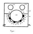
- FIGUREis a schematic representation of an atomic layer deposition arrangement in accordance with the invention.
- a substrateis exposed to two or more atomic layer deposition sources such that a coating is formed on the substrate which provides a barrier to transmission of oxygen and water vapor across the substrate.
- Atomic layer depositionis a method of depositing very thin films onto a surface. Individual precursor gases are pulsed onto the surface, typically a semiconductor wafer, in a sequential manner without mixing the precursors in the gas phase. Each precursor gas reacts with the surface to form an atomic layer in a way such that only one layer at a time can be deposited onto the surface.
- ALD sources 26 and 28are arranged alternately (i.e. in alternating fashion) around process drum 20 . Each ALD source 26 , 28 is enclosed on all sides by a grounded shield 27 except for the side in close proximity to process drum 20 .
- the ALD sourceitself is a linear gas manifold inlet system orientated parallel to the rotational axis of the drum. For those ALD processes requiring surface reactions with activated gases such as oxygen, hydrogen, nitrogen and fluorine, the ALD source from which this gas emerges may be electrical biased. An electrical bias exceeding several hundred volts will plasma-activate the gas into a chemically reactive state.
- the precursor gasis introduced into the ALD chamber 26 at a predetermined flow rate which is balanced by the leak rate of the gas from the shield 27 enclosed space into process chamber 10 .
- Inert gas 30flows into process chamber 10 to entrain the ALD precursor gases and move them along through the chamber exhaust system.
- the gas pressure in process chamber 10is determined by the flow rate of inert gas 30 into chamber 10 and removal through pump 12 of inert gas and gas leaking from the ALD sources 26 , 28 .
- gas pressure in the chamberis less than 100 mtorr, more preferably less than 50 mtorr.
- the pressure in processing chamber 10is maintained at a lower level than the pressure in the ALD sources by controlling the flow rate of inert gas 30 into the chamber and removal of gas by pump 12 .
- the pressure of the precursor gas in the ALD sources 26 , 28is sufficiently high to cover the surface of substrate 14 as it travels over the open end of ALD source 26 , 28 . In this manner, the substrate 14 is alternatively exposed to gas A in ALD source 26 , purge gas in process chamber 10 , and gas B in ALD source 28 as it is conveyed through process chamber 10 .
- process conditionsare arranged such that the monolayer A formed in ALD source 26 chemically reacts with monolayer B formed in ALD source 28 .
- the chemical reactionmay be induced by applying heat to processing drum 20 .
- the aboveis repeated, alternating gas discharge from ALD source 26 and ALD source 28 until the desired thickness of deposition layer is obtained.
- the thickness of the barrier layer according to the inventionis 400 to 100 ⁇ , preferably 200 ⁇ to 50 ⁇ , more preferably 150 ⁇ to 50 ⁇ thick.
- Suitable substratesinclude but are not limited to flexible plastics.
- Preferred plasticsinclude polymers selected from the group consisting of polyethylene terephthalate, polyacrylate, polypropylene, low density polyethylene, high density polyethylene, ethylene vinyl alcohol, polyphenylpropyleneoxide, polyvinyldene chloride and polyamides.
- the thickness of the substrateis typically from 10 ⁇ m to 1600 ⁇ m, preferably 10 ⁇ m to 50 ⁇ m.
- Precursors for making metallized transparent films in ALDare well known to those skilled in the art. Examples of commonly used precursors include O3, Al(CH3)3 and H2O, Al(CH3)3 and O2, Al(CH3)3 and nitrous oxide.
- a PET substrate which is 12 micron thickis unwound from a roll into a drum in a process chamber.
- the drum in the process chamberis treated to 75° C.
- the PET substrateis exposed to a first ALD source which deposits trimethylaluminum and thereafter exposed to an ALD source of oxygen or nitrous oxide at process pressures of 100 mtorr.
- the PET substrateis repeatedly exposed sequentially to a source which deposits trimethylaluminum and thereafter to a source of oxygen or nitrous oxide. This can be achieved by exposing the substrate to the same sources by winding and unwinding substrate over the drum or by providing multiple sources.
- the film thickness corresponding to 100 passes over the ALD sourceswill be approximately 120 ⁇ .
- the coated substrate in accordance with the inventionwill have an oxygen permeability of less than 0.1 cc/m 2 /day, preferably less than 0.010 cc/m 2 /day, most preferably 0.001 cc/m 2 /day and transmission rate for water vapor less than 0.1 g/m 2 /day, preferably 0.01 g/m 2 /day, most preferably 0.001 g/m 2 /day.
Landscapes
- Chemical & Material Sciences (AREA)
- General Chemical & Material Sciences (AREA)
- Chemical Kinetics & Catalysis (AREA)
- Engineering & Computer Science (AREA)
- Materials Engineering (AREA)
- Mechanical Engineering (AREA)
- Metallurgy (AREA)
- Organic Chemistry (AREA)
- Inorganic Chemistry (AREA)
- Laminated Bodies (AREA)
- Physical Vapour Deposition (AREA)
- Chemical Vapour Deposition (AREA)
Abstract
Description
- This invention is directed to an arrangement and process for creating barrier layers on a substrate which form a diffusion barrier for oxygen and water vapor. More particularly, this invention provides an arrangement and process in which barrier layers are formed on plastic substrates using atomic layer deposition. The resulting barrier layers will conform more closely to the substrate surface and reduce the occurrence of pinhole leaks and cracks.
- Food and medical packaging often require low diffusion rates particularly for oxygen and water vapor. Sufficiently low rates of transmission of oxygen and water vapor are exhibited by glass packages such as glass jars, sealed glass vials, etc. Unfortunately glass based packaging is expensive. While polymer based packaging would be less costly, most polymer films with thicknesses useful in packaging application exhibit undesirably high permeability with respect to oxygen and water vapor. Lower gas permeation rates can be achieved by laminating plastic films formed from polymers with barrier materials.
- A well known example of plastic film coated with a barrier material is aluminum coated polyethylene terephthalate (PET). Typically, this coated film material is used for the packaging of food products such as potato chips, peanuts, mini pretzels and the like. The aluminum-coated PET, while exhibiting good barrier properties as a result of the aluminum coating, is not optically transparent and is not compatible with microwave heating ovens.
- Transparent barriers on plastic materials can be formed from alumina, or aluminum oxide and silica or silicon oxide as discussed in Chatham, Hood, Review: Oxygen diffusion barrier properties of transparent oxide coatings on polymeric substrates, Surface and Coatings Technology 78 (1996), pp 1-9. Typically, the silica and alumina are deposited on substrates as thin films, approximately 100-300 Å thick, by either thermal evaporation or by plasma-enhanced chemical vapor deposition (PECVD), for example, as disclosed in U.S. Pat. No. 5,224,441 which is incorporated by reference herein.
- The preparation of thin film barriers on plastics presents several problems. The most significant problem is that polymers have rough surfaces and the films deposited by thermal evaporation or PECVD poorly conform to the undulation of the plastic substrate. For example, the typical average surface roughness of commercially available polyethylene terephthalate (PET) is 8-12 Å root mean square (rms), where 1 Å=10−10m. The barrier performance that can be achieved is limited by the coverage of the surface plastic with the inorganic barrier material. At best, the permeability rate for 12 micron thick PET is decreased by about an order of magnitude for both oxygen and water vapor. While these permeability rates may be sufficient for certain packaging applications, other applications require much lower oxygen and water vapor permeability rates.
- For example, much lower rates are required for plastic films used as substrates for microelectronic circuitry and displays. Organic light emitting diodes (OLEDs) include light emitting materials which rapidly degrade when exposed to minute quantities of oxygen and water vapor. OLED devices must be carefully sealed and protected from water vapor and oxygen. Further, any barrier material used to seal and protect the device from water and oxygen must be transparent to allow emission of light.
- It is an object of the invention to provide an atomic layer deposition arrangement and process to form a barrier layer for substrates which have reduced permeability to oxygen and water vapor.
- Another object of the invention is to provide an atomic layer deposition arrangement and process which provides a barrier layer that closely conforms to a substrate surface.
- A further object of the invention is to provide an atomic layer deposition arrangement and process which provides an optically transparent barrier layer for plastic substrates exhibiting a reduced amount of pinholes and cracks.
- Those and other objects of the invention are achieved by an arrangement including an evacuatable chamber having at least two atomic layer deposition sources located in the chamber. Each atomic layer deposition source is isolated from the remainder of the chamber. A conveyor moves substrate through the evacuatable chamber. In this manner, the substrate is coated with barrier material and exhibits reduced permeability to oxygen and water vapor.
- The invention also provides a method of forming a coated film comprising an atomic layer deposition arrangement comprising an evacuatable chamber having at least two atomic layer deposition sources, each source isolated from the remainder of the chamber. Substrate is conveyed to the first of the at least one atomic layer deposition source, exposing the substrate to the at least one atomic layer deposition source, and then conveyed to the next atomic layer deposition source where it is exposed to that next atomic layer deposition source. After exposing the substrate in this manner to a plurality of sources to form a sufficiently thick layer, such that the coated substrate exhibits reduced permeability to oxygen and water vapor, the coated substrate is conveyed out of the evacuatable chamber or removed from the chamber.
- The attached FIGURE is a schematic representation of an atomic layer deposition arrangement in accordance with the invention.
- In the present invention, a substrate is exposed to two or more atomic layer deposition sources such that a coating is formed on the substrate which provides a barrier to transmission of oxygen and water vapor across the substrate.
- Atomic layer deposition is a method of depositing very thin films onto a surface. Individual precursor gases are pulsed onto the surface, typically a semiconductor wafer, in a sequential manner without mixing the precursors in the gas phase. Each precursor gas reacts with the surface to form an atomic layer in a way such that only one layer at a time can be deposited onto the surface.
- An atomic layer deposition arrangement in accordance with the invention is shown in the attached FIGURE. The atomic layer deposition (“ALD”) arrangement includes a
process chamber 10 which is evacuatable by processing pumps12 (not shown).Substrate 14 is unwound from asupply roll 16 located inwinding chamber 18. Thesubstrate 14 is continuously fed into through and out ofprocess chamber 10, routed over rotating temperature controlledprocessing drum 20 intoprocessing chamber 10, and rewound onrewind drum 22 located inwinding chamber 18. The radial speed of the threedrums substrate 14 into, through and out ofprocess chamber 10. - Fluid communication between
winding chamber 18 andprocess chamber 10 is minimized by minimizingopenings 24 betweenwinding chamber 18 andprocess chamber 10. ALDsources process drum 20. Each ALDsource grounded shield 27 except for the side in close proximity to processdrum 20. The ALD source itself is a linear gas manifold inlet system orientated parallel to the rotational axis of the drum. For those ALD processes requiring surface reactions with activated gases such as oxygen, hydrogen, nitrogen and fluorine, the ALD source from which this gas emerges may be electrical biased. An electrical bias exceeding several hundred volts will plasma-activate the gas into a chemically reactive state. These kinds of sources are well known and described, for example, in U.S. Pat. No. 5,627,435 which is incorporated herein by reference. Preferably the precursor gas is introduced into theALD chamber 26 at a predetermined flow rate which is balanced by the leak rate of the gas from theshield 27 enclosed space intoprocess chamber 10.Inert gas 30 flows intoprocess chamber 10 to entrain the ALD precursor gases and move them along through the chamber exhaust system. The gas pressure inprocess chamber 10 is determined by the flow rate ofinert gas 30 intochamber 10 and removal throughpump 12 of inert gas and gas leaking from theALD sources processing chamber 10 is maintained at a lower level than the pressure in the ALD sources by controlling the flow rate ofinert gas 30 into the chamber and removal of gas bypump 12. The pressure of the precursor gas in theALD sources substrate 14 as it travels over the open end ofALD source substrate 14 is alternatively exposed to gas A inALD source 26, purge gas inprocess chamber 10, and gas B inALD source 28 as it is conveyed throughprocess chamber 10. - In addition, process conditions are arranged such that the monolayer A formed in
ALD source 26 chemically reacts with monolayer B formed inALD source 28. The chemical reaction may be induced by applying heat to processingdrum 20. - The above is repeated, alternating gas discharge from
ALD source 26 andALD source 28 until the desired thickness of deposition layer is obtained. The thickness of the barrier layer according to the invention is 400 to 100 Å, preferably 200 Å to 50 Å, more preferably 150 Å to 50 Å thick. - Suitable substrates include but are not limited to flexible plastics. Preferred plastics include polymers selected from the group consisting of polyethylene terephthalate, polyacrylate, polypropylene, low density polyethylene, high density polyethylene, ethylene vinyl alcohol, polyphenylpropyleneoxide, polyvinyldene chloride and polyamides. The thickness of the substrate is typically from 10 μm to 1600 μm, preferably 10 μm to 50 μm. Precursors for making metallized transparent films in ALD are well known to those skilled in the art. Examples of commonly used precursors include O3, Al(CH3)3 and H2O, Al(CH3)3 and O2, Al(CH3)3 and nitrous oxide.
- The invention will be further described by the following examples which are illustrative only and do not limit the invention.
- A PET substrate which is 12 micron thick is unwound from a roll into a drum in a process chamber. The drum in the process chamber is treated to 75° C. The PET substrate is exposed to a first ALD source which deposits trimethylaluminum and thereafter exposed to an ALD source of oxygen or nitrous oxide at process pressures of 100 mtorr. The PET substrate is repeatedly exposed sequentially to a source which deposits trimethylaluminum and thereafter to a source of oxygen or nitrous oxide. This can be achieved by exposing the substrate to the same sources by winding and unwinding substrate over the drum or by providing multiple sources. The film thickness corresponding to 100 passes over the ALD sources will be approximately 120 Å. Preferably, the coated substrate in accordance with the invention will have an oxygen permeability of less than 0.1 cc/m2/day, preferably less than 0.010 cc/m2/day, most preferably 0.001 cc/m2/day and transmission rate for water vapor less than 0.1 g/m2/day, preferably 0.01 g/m2/day, most preferably 0.001 g/m2/day.
- Although preferred embodiments are specifically illustrated and described herein above, it will be appreciated that many modifications and variations of the present invention are possible in light of the above teachings and within the purview of the appended claims without departing from the spirit and intended scope of the invention.
Claims (20)
Priority Applications (6)
| Application Number | Priority Date | Filing Date | Title |
|---|---|---|---|
| US10/774,841US20050172897A1 (en) | 2004-02-09 | 2004-02-09 | Barrier layer process and arrangement |
| TW094103771ATW200539252A (en) | 2004-02-09 | 2005-02-04 | Barrier layer process and arrangement |
| EP05712844AEP1713950A2 (en) | 2004-02-09 | 2005-02-04 | Barrier layer process and arrangement |
| JP2006552260AJP2007522344A (en) | 2004-02-09 | 2005-02-04 | Barrier layer process and apparatus |
| PCT/US2005/003551WO2005076918A2 (en) | 2004-02-09 | 2005-02-04 | Barrier layer process and arrangement |
| CNA2005800043805ACN1918322A (en) | 2004-02-09 | 2005-02-04 | Barrier layer process and arrangement |
Applications Claiming Priority (1)
| Application Number | Priority Date | Filing Date | Title |
|---|---|---|---|
| US10/774,841US20050172897A1 (en) | 2004-02-09 | 2004-02-09 | Barrier layer process and arrangement |
Publications (1)
| Publication Number | Publication Date |
|---|---|
| US20050172897A1true US20050172897A1 (en) | 2005-08-11 |
Family
ID=34827064
Family Applications (1)
| Application Number | Title | Priority Date | Filing Date |
|---|---|---|---|
| US10/774,841AbandonedUS20050172897A1 (en) | 2004-02-09 | 2004-02-09 | Barrier layer process and arrangement |
Country Status (6)
| Country | Link |
|---|---|
| US (1) | US20050172897A1 (en) |
| EP (1) | EP1713950A2 (en) |
| JP (1) | JP2007522344A (en) |
| CN (1) | CN1918322A (en) |
| TW (1) | TW200539252A (en) |
| WO (1) | WO2005076918A2 (en) |
Cited By (30)
| Publication number | Priority date | Publication date | Assignee | Title |
|---|---|---|---|---|
| US20050186338A1 (en)* | 2004-02-19 | 2005-08-25 | Nanosolar, Inc. | High throughput surface treatment on coiled flexible substrates |
| US20070224348A1 (en)* | 2006-03-26 | 2007-09-27 | Planar Systems, Inc. | Atomic layer deposition system and method for coating flexible substrates |
| US20070281089A1 (en)* | 2006-06-05 | 2007-12-06 | General Electric Company | Systems and methods for roll-to-roll atomic layer deposition on continuously fed objects |
| US20080138539A1 (en)* | 2006-12-06 | 2008-06-12 | General Electric Company | Barrier layer, composite article comprising the same, electroactive device, and method |
| US20080182101A1 (en)* | 2003-05-16 | 2008-07-31 | Peter Francis Carcia | Barrier films for plastic substrates fabricated by atomic layer deposition |
| EP2009138A1 (en)* | 2007-06-28 | 2008-12-31 | Siemens Energy, Inc. | Atomic layer epitaxy processed insulation |
| US20090032108A1 (en)* | 2007-03-30 | 2009-02-05 | Craig Leidholm | Formation of photovoltaic absorber layers on foil substrates |
| WO2009031886A3 (en)* | 2007-09-07 | 2009-06-04 | Fujifilm Mfg Europe Bv | Method and apparatus for atomic layer deposition using an atmospheric pressure glow discharge plasma |
| EP1992007A4 (en)* | 2006-03-03 | 2010-05-05 | Prasad Gadgil | Apparatus and method for large area multi-layer atomic layer chemical vapor processing of thin films |
| US20110159204A1 (en)* | 2009-12-29 | 2011-06-30 | Lotus Applied Technology, Llc | Oxygen radical generation for radical-enhanced thin film deposition |
| FR2956869A1 (en)* | 2010-03-01 | 2011-09-02 | Alex Hr Roustaei | SYSTEM FOR PRODUCING HIGH CAPACITY FLEXIBLE FILM FOR PHOTOVOLTAIC AND OLED CELLS BY CYCLIC LAYER DEPOSITION |
| WO2011156484A3 (en)* | 2010-06-08 | 2012-01-26 | President And Fellows Of Harvard College | Low-temperature synthesis of silica |
| WO2012028776A1 (en)* | 2010-08-30 | 2012-03-08 | Beneq Oy | Apparatus |
| WO2012028780A1 (en)* | 2010-08-30 | 2012-03-08 | Beneq Oy | Nozzle head and apparatus |
| EP2557198A1 (en)* | 2011-08-10 | 2013-02-13 | Nederlandse Organisatie voor toegepast -natuurwetenschappelijk onderzoek TNO | Method and apparatus for depositing atomic layers on a substrate |
| US20130064977A1 (en)* | 2010-02-11 | 2013-03-14 | Nederlandse Organisatie Voor Toegepast-Natuurweten Schappelijk Onderzoek Tno | Method and apparatus for depositing atomic layers on a substrate |
| US8637117B2 (en) | 2009-10-14 | 2014-01-28 | Lotus Applied Technology, Llc | Inhibiting excess precursor transport between separate precursor zones in an atomic layer deposition system |
| US20140295196A1 (en)* | 2013-03-29 | 2014-10-02 | Industrial Technology Research Institute | Composite film and manufacturing method of the same |
| WO2014167313A1 (en)* | 2013-04-09 | 2014-10-16 | Innovia Films Limited | Uv protected films |
| US8927315B1 (en) | 2005-01-20 | 2015-01-06 | Aeris Capital Sustainable Ip Ltd. | High-throughput assembly of series interconnected solar cells |
| EP2122005B1 (en) | 2007-01-08 | 2015-11-11 | Eastman Kodak Company | Deposition system and method |
| US9243322B2 (en) | 2011-10-31 | 2016-01-26 | 3M Innovative Properties Company | Methods for applying a coating to a substrate in rolled form |
| US9297076B2 (en) | 2010-07-23 | 2016-03-29 | Lotus Applied Technology, Llc | Substrate transport mechanism contacting a single side of a flexible web substrate for roll-to-roll thin film deposition |
| US9435028B2 (en) | 2013-05-06 | 2016-09-06 | Lotus Applied Technology, Llc | Plasma generation for thin film deposition on flexible substrates |
| GB2536572A (en)* | 2015-03-18 | 2016-09-21 | Ardenne Gmbh Von | Tape-substrate coating line having a magnetron arrangement |
| US9687868B2 (en) | 2012-05-31 | 2017-06-27 | Toppan Printing Co., Ltd. | Rolled film formation apparatus |
| US9909212B2 (en) | 2010-08-30 | 2018-03-06 | Beneq Oy | Apparatus for processing substrate surface |
| WO2021247380A1 (en)* | 2020-06-04 | 2021-12-09 | Applied Materials, Inc. | Vapor deposition apparatus and method for coating a substrate in a vacuum chamber |
| WO2022124897A1 (en)* | 2020-12-08 | 2022-06-16 | Kalpana Technologies B.V. | Roll-to-roll processing |
| US20220267902A1 (en)* | 2019-08-30 | 2022-08-25 | Meidensha Corporation | Atomic layer deposition device and atomic layer deposition method |
Families Citing this family (11)
| Publication number | Priority date | Publication date | Assignee | Title |
|---|---|---|---|---|
| SE534932C2 (en)* | 2009-12-21 | 2012-02-21 | Stora Enso Oyj | A paper or cardboard substrate, a process for manufacturing the substrate and a package formed from the substrate |
| JP5621258B2 (en)* | 2009-12-28 | 2014-11-12 | ソニー株式会社 | Film forming apparatus and film forming method |
| JP5912228B2 (en)* | 2010-05-17 | 2016-04-27 | 凸版印刷株式会社 | Method for producing gas barrier laminate |
| FI20105902A0 (en)* | 2010-08-30 | 2010-08-30 | Beneq Oy | Device |
| JP5768962B2 (en)* | 2011-03-23 | 2015-08-26 | 凸版印刷株式会社 | Film formation processing drum in atomic layer deposition method film formation apparatus |
| EP2692899B1 (en) | 2011-03-29 | 2017-04-19 | Toppan Printing Co., Ltd. | Roll to roll atomic layer deposition (ald) |
| TWI590951B (en) | 2011-07-28 | 2017-07-11 | 凸版印刷股份有限公司 | Layered product, gas barrier film, manufacturing method of layered product, and layered product manufacturing apparatus |
| JP6028711B2 (en)* | 2013-10-23 | 2016-11-16 | 住友金属鉱山株式会社 | Double-sided film forming method and method for producing resin film with metal base layer |
| EP3054032B1 (en) | 2015-02-09 | 2017-08-23 | Coating Plasma Industrie | Installation for film deposition onto and/or modification of the surface of a moving substrate |
| NL2015215B1 (en)* | 2015-07-23 | 2017-02-08 | Meyer Burger (Netherlands) B V | Programmable deposition apparatus. |
| EP3914750A4 (en)* | 2019-01-25 | 2023-02-15 | Applied Materials, Inc. | Method of forming moisture and oxygen barrier coatings |
Citations (10)
| Publication number | Priority date | Publication date | Assignee | Title |
|---|---|---|---|---|
| US4058430A (en)* | 1974-11-29 | 1977-11-15 | Tuomo Suntola | Method for producing compound thin films |
| US4692233A (en)* | 1983-04-06 | 1987-09-08 | General Engineering Radcliffe Limited | Vacuum coating apparatus |
| US5224441A (en)* | 1991-09-27 | 1993-07-06 | The Boc Group, Inc. | Apparatus for rapid plasma treatments and method |
| US5300189A (en)* | 1986-05-21 | 1994-04-05 | Hitachi, Ltd. | Plasma surface treatment method and apparatus |
| US5627435A (en)* | 1993-07-12 | 1997-05-06 | The Boc Group, Inc. | Hollow cathode array and method of cleaning sheet stock therewith |
| US6312524B1 (en)* | 1996-09-10 | 2001-11-06 | Hitachi Maxell, Ltd. | Plasma CVD apparatus |
| US6368889B1 (en)* | 1998-10-22 | 2002-04-09 | Japan Science And Technology Corporation | Variable-wavelength light-emitting device and method of manufacture |
| US20020043216A1 (en)* | 2000-08-09 | 2002-04-18 | Chul-Ju Hwang | Atomic layer deposition method and semiconductor device fabricating apparatus having rotatable gas injectors |
| US20030026989A1 (en)* | 2000-06-21 | 2003-02-06 | George Steven M. | Insulating and functionalizing fine metal-containing particles with conformal ultra-thin films |
| US20030207032A1 (en)* | 2002-05-02 | 2003-11-06 | Micron Technology, Inc. | Methods, systems, and apparatus for atomic-layer deposition of aluminum oxides in integrated circuits |
Family Cites Families (1)
| Publication number | Priority date | Publication date | Assignee | Title |
|---|---|---|---|---|
| EP1425110B1 (en)* | 2001-07-18 | 2014-09-03 | The Regents of the University of Colorado | A method of depositing an inorganic film on an organic polymer |
- 2004
- 2004-02-09USUS10/774,841patent/US20050172897A1/ennot_activeAbandoned
- 2005
- 2005-02-04TWTW094103771Apatent/TW200539252A/enunknown
- 2005-02-04WOPCT/US2005/003551patent/WO2005076918A2/ennot_activeApplication Discontinuation
- 2005-02-04CNCNA2005800043805Apatent/CN1918322A/enactivePending
- 2005-02-04EPEP05712844Apatent/EP1713950A2/ennot_activeWithdrawn
- 2005-02-04JPJP2006552260Apatent/JP2007522344A/enactivePending
Patent Citations (10)
| Publication number | Priority date | Publication date | Assignee | Title |
|---|---|---|---|---|
| US4058430A (en)* | 1974-11-29 | 1977-11-15 | Tuomo Suntola | Method for producing compound thin films |
| US4692233A (en)* | 1983-04-06 | 1987-09-08 | General Engineering Radcliffe Limited | Vacuum coating apparatus |
| US5300189A (en)* | 1986-05-21 | 1994-04-05 | Hitachi, Ltd. | Plasma surface treatment method and apparatus |
| US5224441A (en)* | 1991-09-27 | 1993-07-06 | The Boc Group, Inc. | Apparatus for rapid plasma treatments and method |
| US5627435A (en)* | 1993-07-12 | 1997-05-06 | The Boc Group, Inc. | Hollow cathode array and method of cleaning sheet stock therewith |
| US6312524B1 (en)* | 1996-09-10 | 2001-11-06 | Hitachi Maxell, Ltd. | Plasma CVD apparatus |
| US6368889B1 (en)* | 1998-10-22 | 2002-04-09 | Japan Science And Technology Corporation | Variable-wavelength light-emitting device and method of manufacture |
| US20030026989A1 (en)* | 2000-06-21 | 2003-02-06 | George Steven M. | Insulating and functionalizing fine metal-containing particles with conformal ultra-thin films |
| US20020043216A1 (en)* | 2000-08-09 | 2002-04-18 | Chul-Ju Hwang | Atomic layer deposition method and semiconductor device fabricating apparatus having rotatable gas injectors |
| US20030207032A1 (en)* | 2002-05-02 | 2003-11-06 | Micron Technology, Inc. | Methods, systems, and apparatus for atomic-layer deposition of aluminum oxides in integrated circuits |
Cited By (61)
| Publication number | Priority date | Publication date | Assignee | Title |
|---|---|---|---|---|
| US8445937B2 (en) | 2003-05-16 | 2013-05-21 | E I Du Pont De Nemours And Company | Barrier films for plastic substrates fabricated by atomic layer deposition |
| US20080182101A1 (en)* | 2003-05-16 | 2008-07-31 | Peter Francis Carcia | Barrier films for plastic substrates fabricated by atomic layer deposition |
| US7115304B2 (en)* | 2004-02-19 | 2006-10-03 | Nanosolar, Inc. | High throughput surface treatment on coiled flexible substrates |
| US7858151B2 (en) | 2004-02-19 | 2010-12-28 | Nanosolar, Inc. | Formation of CIGS absorber layer materials using atomic layer deposition and high throughput surface treatment |
| US20110189815A1 (en)* | 2004-02-19 | 2011-08-04 | Sager Brian M | Formation of cigs absorber layer materials using atomic layer deposition and high throughput surface treatment on coiled flexible substrates |
| US20050186338A1 (en)* | 2004-02-19 | 2005-08-25 | Nanosolar, Inc. | High throughput surface treatment on coiled flexible substrates |
| US8927315B1 (en) | 2005-01-20 | 2015-01-06 | Aeris Capital Sustainable Ip Ltd. | High-throughput assembly of series interconnected solar cells |
| EP1992007A4 (en)* | 2006-03-03 | 2010-05-05 | Prasad Gadgil | Apparatus and method for large area multi-layer atomic layer chemical vapor processing of thin films |
| EP2000008A4 (en)* | 2006-03-26 | 2010-05-05 | Lotus Applied Technology Llc | ATOMIC LAYER DEPOSITION DEVICE AND METHOD FOR COATING FLEXIBLE SUBSTRATES |
| US8137464B2 (en) | 2006-03-26 | 2012-03-20 | Lotus Applied Technology, Llc | Atomic layer deposition system for coating flexible substrates |
| US8202366B2 (en) | 2006-03-26 | 2012-06-19 | Lotus Applied Technology, Llc | Atomic layer deposition system utilizing multiple precursor zones for coating flexible substrates |
| US20100189900A1 (en)* | 2006-03-26 | 2010-07-29 | Lotus Applied Technology, Llc | Atomic layer deposition system and method utilizing multiple precursor zones for coating flexible substrates |
| US9238868B2 (en) | 2006-03-26 | 2016-01-19 | Lotus Applied Technology, Llc | Atomic layer deposition method for coating flexible substrates |
| US9469901B2 (en) | 2006-03-26 | 2016-10-18 | Lotus Applied Techonology, Llc | Atomic layer deposition method utilizing multiple precursor zones for coating flexible substrates |
| US20070224348A1 (en)* | 2006-03-26 | 2007-09-27 | Planar Systems, Inc. | Atomic layer deposition system and method for coating flexible substrates |
| WO2008057625A3 (en)* | 2006-06-05 | 2009-03-19 | Gen Electric | Systems and methods for roll-to-roll atomic layer deposition on continuously fed objects |
| US20070281089A1 (en)* | 2006-06-05 | 2007-12-06 | General Electric Company | Systems and methods for roll-to-roll atomic layer deposition on continuously fed objects |
| US20080138539A1 (en)* | 2006-12-06 | 2008-06-12 | General Electric Company | Barrier layer, composite article comprising the same, electroactive device, and method |
| US7781031B2 (en) | 2006-12-06 | 2010-08-24 | General Electric Company | Barrier layer, composite article comprising the same, electroactive device, and method |
| EP3002346B1 (en) | 2007-01-08 | 2018-01-24 | Eastman Kodak Company | Deposition method |
| US10351954B2 (en) | 2007-01-08 | 2019-07-16 | Eastman Kodak Company | Deposition system and method using a delivery head separated from a substrate by gas pressure |
| US11136667B2 (en)* | 2007-01-08 | 2021-10-05 | Eastman Kodak Company | Deposition system and method using a delivery head separated from a substrate by gas pressure |
| EP2122005B1 (en) | 2007-01-08 | 2015-11-11 | Eastman Kodak Company | Deposition system and method |
| US20090032108A1 (en)* | 2007-03-30 | 2009-02-05 | Craig Leidholm | Formation of photovoltaic absorber layers on foil substrates |
| US7947128B2 (en) | 2007-06-28 | 2011-05-24 | Siemens Energy, Inc. | Atomic layer epitaxy processed insulation |
| US20090000541A1 (en)* | 2007-06-28 | 2009-01-01 | Siemens Power Generation, Inc. | Atomic layer epitaxy processed insulation |
| EP2009138A1 (en)* | 2007-06-28 | 2008-12-31 | Siemens Energy, Inc. | Atomic layer epitaxy processed insulation |
| US20100255625A1 (en)* | 2007-09-07 | 2010-10-07 | Fujifilm Manufacturing Europe B.V. | Method and apparatus for atomic layer deposition using an atmospheric pressure glow discharge plasma |
| WO2009031886A3 (en)* | 2007-09-07 | 2009-06-04 | Fujifilm Mfg Europe Bv | Method and apparatus for atomic layer deposition using an atmospheric pressure glow discharge plasma |
| US8637117B2 (en) | 2009-10-14 | 2014-01-28 | Lotus Applied Technology, Llc | Inhibiting excess precursor transport between separate precursor zones in an atomic layer deposition system |
| US8637123B2 (en) | 2009-12-29 | 2014-01-28 | Lotus Applied Technology, Llc | Oxygen radical generation for radical-enhanced thin film deposition |
| US20110159204A1 (en)* | 2009-12-29 | 2011-06-30 | Lotus Applied Technology, Llc | Oxygen radical generation for radical-enhanced thin film deposition |
| US20130064977A1 (en)* | 2010-02-11 | 2013-03-14 | Nederlandse Organisatie Voor Toegepast-Natuurweten Schappelijk Onderzoek Tno | Method and apparatus for depositing atomic layers on a substrate |
| US9297077B2 (en)* | 2010-02-11 | 2016-03-29 | Nederlandse Organisatie Voor Toegepast-Natuurwetenschappelijk Onderzoek Tno | Method and apparatus for depositing atomic layers on a substrate |
| FR2956869A1 (en)* | 2010-03-01 | 2011-09-02 | Alex Hr Roustaei | SYSTEM FOR PRODUCING HIGH CAPACITY FLEXIBLE FILM FOR PHOTOVOLTAIC AND OLED CELLS BY CYCLIC LAYER DEPOSITION |
| AU2011264922B2 (en)* | 2010-06-08 | 2015-11-26 | President And Fellows Of Harvard College | Low-temperature synthesis of silica |
| WO2011156484A3 (en)* | 2010-06-08 | 2012-01-26 | President And Fellows Of Harvard College | Low-temperature synthesis of silica |
| US9297076B2 (en) | 2010-07-23 | 2016-03-29 | Lotus Applied Technology, Llc | Substrate transport mechanism contacting a single side of a flexible web substrate for roll-to-roll thin film deposition |
| WO2012028776A1 (en)* | 2010-08-30 | 2012-03-08 | Beneq Oy | Apparatus |
| US9909212B2 (en) | 2010-08-30 | 2018-03-06 | Beneq Oy | Apparatus for processing substrate surface |
| WO2012028780A1 (en)* | 2010-08-30 | 2012-03-08 | Beneq Oy | Nozzle head and apparatus |
| US9803281B2 (en) | 2010-08-30 | 2017-10-31 | Beneq Oy | Nozzle head and apparatus |
| US9567671B2 (en) | 2011-08-10 | 2017-02-14 | Nederlandse Organisatie Voor Toegepast-Natuurwetenschappelijk Onderzoek Tno | Method and apparatus for depositing atomic layers on a substrate |
| KR20140064851A (en)* | 2011-08-10 | 2014-05-28 | 네덜란제 오르가니자티에 포오르 토에게파스트-나투우르베텐샤펠리즈크 온데르조에크 테엔오 | Method and apparatus for depositing atomic layers on a substrate |
| EP2557198A1 (en)* | 2011-08-10 | 2013-02-13 | Nederlandse Organisatie voor toegepast -natuurwetenschappelijk onderzoek TNO | Method and apparatus for depositing atomic layers on a substrate |
| WO2013022339A1 (en)* | 2011-08-10 | 2013-02-14 | Nederlandse Organisatie Voor Toegepast-Natuurwetenschappelijk Onderzoek Tno | Method and apparatus for depositing atomic layers on a substrate |
| KR101942605B1 (en) | 2011-08-10 | 2019-01-25 | 네덜란제 오르가니자티에 포오르 토에게파스트-나투우르베텐샤펠리즈크 온데르조에크 테엔오 | Method and apparatus for depositing atomic layers on a substrate |
| US9243322B2 (en) | 2011-10-31 | 2016-01-26 | 3M Innovative Properties Company | Methods for applying a coating to a substrate in rolled form |
| US9687868B2 (en) | 2012-05-31 | 2017-06-27 | Toppan Printing Co., Ltd. | Rolled film formation apparatus |
| US20140295196A1 (en)* | 2013-03-29 | 2014-10-02 | Industrial Technology Research Institute | Composite film and manufacturing method of the same |
| WO2014167313A1 (en)* | 2013-04-09 | 2014-10-16 | Innovia Films Limited | Uv protected films |
| US9435028B2 (en) | 2013-05-06 | 2016-09-06 | Lotus Applied Technology, Llc | Plasma generation for thin film deposition on flexible substrates |
| GB2536572A (en)* | 2015-03-18 | 2016-09-21 | Ardenne Gmbh Von | Tape-substrate coating line having a magnetron arrangement |
| US20220267902A1 (en)* | 2019-08-30 | 2022-08-25 | Meidensha Corporation | Atomic layer deposition device and atomic layer deposition method |
| US11680319B2 (en)* | 2019-08-30 | 2023-06-20 | Meidensha Corporation | Atomic layer deposition device and atomic layer deposition method |
| WO2021247380A1 (en)* | 2020-06-04 | 2021-12-09 | Applied Materials, Inc. | Vapor deposition apparatus and method for coating a substrate in a vacuum chamber |
| CN115667574A (en)* | 2020-06-04 | 2023-01-31 | 应用材料公司 | Vapor deposition apparatus and method of coating a substrate in a vacuum chamber |
| US11732345B2 (en) | 2020-06-04 | 2023-08-22 | Applied Materials, Inc. | Vapor deposition apparatus and method for coating a substrate in a vacuum chamber |
| WO2022124897A1 (en)* | 2020-12-08 | 2022-06-16 | Kalpana Technologies B.V. | Roll-to-roll processing |
| NL2027074B1 (en)* | 2020-12-08 | 2022-07-07 | Kalpana Tech B V | Roll-to-roll processing |
| CN116867926A (en)* | 2020-12-08 | 2023-10-10 | 卡尔帕纳科技私人有限公司 | Roll-to-roll processing |
Also Published As
| Publication number | Publication date |
|---|---|
| TW200539252A (en) | 2005-12-01 |
| EP1713950A2 (en) | 2006-10-25 |
| CN1918322A (en) | 2007-02-21 |
| JP2007522344A (en) | 2007-08-09 |
| WO2005076918A2 (en) | 2005-08-25 |
| WO2005076918A3 (en) | 2006-10-19 |
Similar Documents
| Publication | Publication Date | Title |
|---|---|---|
| US20050172897A1 (en) | Barrier layer process and arrangement | |
| JP5267713B2 (en) | Transparent gas barrier film, method for producing the same, and organic electroluminescence device | |
| US7976899B2 (en) | Methods for selective deposition of graded materials on continuously fed objects | |
| US20100092781A1 (en) | Roll-To-Roll Plasma Enhanced Chemical Vapor Deposition Method of Barrier Layers Comprising Silicon And Carbon | |
| US8871350B2 (en) | Gas barrier film, electronic device including the same, gas barrier bag, and method for producing gas barrier film | |
| US20100143710A1 (en) | High rate deposition of thin films with improved barrier layer properties | |
| JP2004160977A (en) | Barrier layer for article and process of forming the barrier layer using expanding thermal plasma | |
| JP2012184509A (en) | Barrier structure comprising substrate film and barrier coating, and article comprising the same | |
| EP2732071B1 (en) | Mixed metal oxide barrier films and atomic layer deposition method for making mixed metal oxide barrier films | |
| US20090011146A1 (en) | Method of Forming Vapor Deposited Layer by Surface-Wave Plasma and Apparatus Therefor | |
| US10961622B2 (en) | Gas barrier film and method of manufacturing the same | |
| KR102450786B1 (en) | Laminate and its manufacturing method | |
| US8512809B2 (en) | Method of processing multilayer film | |
| US20070148346A1 (en) | Systems and methods for deposition of graded materials on continuously fed objects | |
| JP5719106B2 (en) | Transparent gas barrier film and method for producing transparent gas barrier film | |
| JP5300765B2 (en) | Gas barrier film | |
| JP2005219427A (en) | Barrier film manufacturing method and plasma CVD apparatus used therefor | |
| WO2015163358A1 (en) | Gas barrier film and manufacturing method thereof | |
| JP2016074927A (en) | Film deposition device and film deposition method | |
| JPH10317148A (en) | Manufacture of gas barrier type plastic film |
Legal Events
| Date | Code | Title | Description |
|---|---|---|---|
| AS | Assignment | Owner name:BOC GROUP, INC., THE, NEW JERSEY Free format text:ASSIGNMENT OF ASSIGNORS INTEREST;ASSIGNOR:JANSEN, FRANK;REEL/FRAME:015448/0631 Effective date:20040520 | |
| AS | Assignment | Owner name:BOC EDWARDS, INC., MASSACHUSETTS Free format text:ASSIGNMENT OF ASSIGNORS INTEREST;ASSIGNOR:THE BOC GROUP, INC.;REEL/FRAME:019767/0251 Effective date:20070330 Owner name:BOC EDWARDS, INC.,MASSACHUSETTS Free format text:ASSIGNMENT OF ASSIGNORS INTEREST;ASSIGNOR:THE BOC GROUP, INC.;REEL/FRAME:019767/0251 Effective date:20070330 | |
| AS | Assignment | Owner name:EDWARDS VACUUM, INC., MASSACHUSETTS Free format text:CHANGE OF NAME;ASSIGNOR:BOC EDWARDS, INC.;REEL/FRAME:020654/0963 Effective date:20070920 Owner name:EDWARDS VACUUM, INC.,MASSACHUSETTS Free format text:CHANGE OF NAME;ASSIGNOR:BOC EDWARDS, INC.;REEL/FRAME:020654/0963 Effective date:20070920 | |
| STCB | Information on status: application discontinuation | Free format text:ABANDONED -- FAILURE TO RESPOND TO AN OFFICE ACTION |