US20050170558A1 - Method of forming a stack of packaged memory dice - Google Patents
Method of forming a stack of packaged memory diceDownload PDFInfo
- Publication number
- US20050170558A1 US20050170558A1US11/092,348US9234805AUS2005170558A1US 20050170558 A1US20050170558 A1US 20050170558A1US 9234805 AUS9234805 AUS 9234805AUS 2005170558 A1US2005170558 A1US 2005170558A1
- Authority
- US
- United States
- Prior art keywords
- multiconductor
- assembly
- semiconductor device
- terminals
- integrated circuit
- Prior art date
- Legal status (The legal status is an assumption and is not a legal conclusion. Google has not performed a legal analysis and makes no representation as to the accuracy of the status listed.)
- Granted
Links
Images


Classifications
- H—ELECTRICITY
- H01—ELECTRIC ELEMENTS
- H01L—SEMICONDUCTOR DEVICES NOT COVERED BY CLASS H10
- H01L25/00—Assemblies consisting of a plurality of semiconductor or other solid state devices
- H01L25/03—Assemblies consisting of a plurality of semiconductor or other solid state devices all the devices being of a type provided for in a single subclass of subclasses H10B, H10D, H10F, H10H, H10K or H10N, e.g. assemblies of rectifier diodes
- H01L25/04—Assemblies consisting of a plurality of semiconductor or other solid state devices all the devices being of a type provided for in a single subclass of subclasses H10B, H10D, H10F, H10H, H10K or H10N, e.g. assemblies of rectifier diodes the devices not having separate containers
- H01L25/065—Assemblies consisting of a plurality of semiconductor or other solid state devices all the devices being of a type provided for in a single subclass of subclasses H10B, H10D, H10F, H10H, H10K or H10N, e.g. assemblies of rectifier diodes the devices not having separate containers the devices being of a type provided for in group H10D89/00
- H01L25/0657—Stacked arrangements of devices
- H—ELECTRICITY
- H01—ELECTRIC ELEMENTS
- H01L—SEMICONDUCTOR DEVICES NOT COVERED BY CLASS H10
- H01L25/00—Assemblies consisting of a plurality of semiconductor or other solid state devices
- H01L25/03—Assemblies consisting of a plurality of semiconductor or other solid state devices all the devices being of a type provided for in a single subclass of subclasses H10B, H10D, H10F, H10H, H10K or H10N, e.g. assemblies of rectifier diodes
- H01L25/10—Assemblies consisting of a plurality of semiconductor or other solid state devices all the devices being of a type provided for in a single subclass of subclasses H10B, H10D, H10F, H10H, H10K or H10N, e.g. assemblies of rectifier diodes the devices having separate containers
- H01L25/105—Assemblies consisting of a plurality of semiconductor or other solid state devices all the devices being of a type provided for in a single subclass of subclasses H10B, H10D, H10F, H10H, H10K or H10N, e.g. assemblies of rectifier diodes the devices having separate containers the devices being integrated devices of class H10
- H—ELECTRICITY
- H01—ELECTRIC ELEMENTS
- H01L—SEMICONDUCTOR DEVICES NOT COVERED BY CLASS H10
- H01L2225/00—Details relating to assemblies covered by the group H01L25/00 but not provided for in its subgroups
- H01L2225/03—All the devices being of a type provided for in the same main group of the same subclass of class H10, e.g. assemblies of rectifier diodes
- H01L2225/04—All the devices being of a type provided for in the same main group of the same subclass of class H10, e.g. assemblies of rectifier diodes the devices not having separate containers
- H01L2225/065—All the devices being of a type provided for in the same main group of the same subclass of class H10
- H01L2225/06503—Stacked arrangements of devices
- H01L2225/06551—Conductive connections on the side of the device
- H—ELECTRICITY
- H01—ELECTRIC ELEMENTS
- H01L—SEMICONDUCTOR DEVICES NOT COVERED BY CLASS H10
- H01L2225/00—Details relating to assemblies covered by the group H01L25/00 but not provided for in its subgroups
- H01L2225/03—All the devices being of a type provided for in the same main group of the same subclass of class H10, e.g. assemblies of rectifier diodes
- H01L2225/04—All the devices being of a type provided for in the same main group of the same subclass of class H10, e.g. assemblies of rectifier diodes the devices not having separate containers
- H01L2225/065—All the devices being of a type provided for in the same main group of the same subclass of class H10
- H01L2225/06503—Stacked arrangements of devices
- H01L2225/06579—TAB carriers; beam leads
- H—ELECTRICITY
- H01—ELECTRIC ELEMENTS
- H01L—SEMICONDUCTOR DEVICES NOT COVERED BY CLASS H10
- H01L2225/00—Details relating to assemblies covered by the group H01L25/00 but not provided for in its subgroups
- H01L2225/03—All the devices being of a type provided for in the same main group of the same subclass of class H10, e.g. assemblies of rectifier diodes
- H01L2225/04—All the devices being of a type provided for in the same main group of the same subclass of class H10, e.g. assemblies of rectifier diodes the devices not having separate containers
- H01L2225/065—All the devices being of a type provided for in the same main group of the same subclass of class H10
- H01L2225/06503—Stacked arrangements of devices
- H01L2225/06582—Housing for the assembly, e.g. chip scale package [CSP]
- H—ELECTRICITY
- H01—ELECTRIC ELEMENTS
- H01L—SEMICONDUCTOR DEVICES NOT COVERED BY CLASS H10
- H01L2225/00—Details relating to assemblies covered by the group H01L25/00 but not provided for in its subgroups
- H01L2225/03—All the devices being of a type provided for in the same main group of the same subclass of class H10, e.g. assemblies of rectifier diodes
- H01L2225/10—All the devices being of a type provided for in the same main group of the same subclass of class H10, e.g. assemblies of rectifier diodes the devices having separate containers
- H01L2225/1005—All the devices being of a type provided for in the same main group of the same subclass of class H10, e.g. assemblies of rectifier diodes the devices having separate containers the devices being integrated devices of class H10
- H01L2225/1011—All the devices being of a type provided for in the same main group of the same subclass of class H10, e.g. assemblies of rectifier diodes the devices having separate containers the devices being integrated devices of class H10 the containers being in a stacked arrangement
- H01L2225/1017—All the devices being of a type provided for in the same main group of the same subclass of class H10, e.g. assemblies of rectifier diodes the devices having separate containers the devices being integrated devices of class H10 the containers being in a stacked arrangement the lowermost container comprising a device support
- H01L2225/1029—All the devices being of a type provided for in the same main group of the same subclass of class H10, e.g. assemblies of rectifier diodes the devices having separate containers the devices being integrated devices of class H10 the containers being in a stacked arrangement the lowermost container comprising a device support the support being a lead frame
- H—ELECTRICITY
- H01—ELECTRIC ELEMENTS
- H01L—SEMICONDUCTOR DEVICES NOT COVERED BY CLASS H10
- H01L2225/00—Details relating to assemblies covered by the group H01L25/00 but not provided for in its subgroups
- H01L2225/03—All the devices being of a type provided for in the same main group of the same subclass of class H10, e.g. assemblies of rectifier diodes
- H01L2225/10—All the devices being of a type provided for in the same main group of the same subclass of class H10, e.g. assemblies of rectifier diodes the devices having separate containers
- H01L2225/1005—All the devices being of a type provided for in the same main group of the same subclass of class H10, e.g. assemblies of rectifier diodes the devices having separate containers the devices being integrated devices of class H10
- H01L2225/1011—All the devices being of a type provided for in the same main group of the same subclass of class H10, e.g. assemblies of rectifier diodes the devices having separate containers the devices being integrated devices of class H10 the containers being in a stacked arrangement
- H01L2225/1047—Details of electrical connections between containers
- H01L2225/1064—Electrical connections provided on a side surface of one or more of the containers
- H—ELECTRICITY
- H01—ELECTRIC ELEMENTS
- H01L—SEMICONDUCTOR DEVICES NOT COVERED BY CLASS H10
- H01L2225/00—Details relating to assemblies covered by the group H01L25/00 but not provided for in its subgroups
- H01L2225/03—All the devices being of a type provided for in the same main group of the same subclass of class H10, e.g. assemblies of rectifier diodes
- H01L2225/10—All the devices being of a type provided for in the same main group of the same subclass of class H10, e.g. assemblies of rectifier diodes the devices having separate containers
- H01L2225/1005—All the devices being of a type provided for in the same main group of the same subclass of class H10, e.g. assemblies of rectifier diodes the devices having separate containers the devices being integrated devices of class H10
- H01L2225/1011—All the devices being of a type provided for in the same main group of the same subclass of class H10, e.g. assemblies of rectifier diodes the devices having separate containers the devices being integrated devices of class H10 the containers being in a stacked arrangement
- H01L2225/1047—Details of electrical connections between containers
- H01L2225/107—Indirect electrical connections, e.g. via an interposer, a flexible substrate, using TAB
- H—ELECTRICITY
- H01—ELECTRIC ELEMENTS
- H01L—SEMICONDUCTOR DEVICES NOT COVERED BY CLASS H10
- H01L2924/00—Indexing scheme for arrangements or methods for connecting or disconnecting semiconductor or solid-state bodies as covered by H01L24/00
- H01L2924/0001—Technical content checked by a classifier
- H01L2924/00014—Technical content checked by a classifier the subject-matter covered by the group, the symbol of which is combined with the symbol of this group, being disclosed without further technical details
- H—ELECTRICITY
- H01—ELECTRIC ELEMENTS
- H01L—SEMICONDUCTOR DEVICES NOT COVERED BY CLASS H10
- H01L2924/00—Indexing scheme for arrangements or methods for connecting or disconnecting semiconductor or solid-state bodies as covered by H01L24/00
- H01L2924/01—Chemical elements
- H01L2924/01047—Silver [Ag]
Definitions
- the inventionrelates to packaged integrated circuit devices. More specifically, the present invention relates to an interconnected stack of packaged memory devices and the method of forming a stack of interconnected packaged memory devices.
- the lead frameincludes a plurality of leads having their ends terminating adjacent a side or edge of an integrated circuit semiconductor device supported by the die paddle portion of the lead frame. Electrical connections are made by means of wire bonds extending between the leads of the lead frame and the bond pads located on the active surface of the integrated circuit semiconductor device. Subsequent to the wire bonding operation, portions of the leads of the lead frame and the integrated circuit semiconductor device are encapsulated in suitable plastic material to form a packaged semiconductor device. The leads and lead frame are then trimmed and formed to the desired configuration after the packaging of the semiconductor device in the encapsulant material.
- the leads of the lead frameextend over the active surface of the semiconductor device being insulated therefrom by tape which is adhesively bonded to the semiconductor device and the leads of the lead frame. Electrical connections are made between the leads of the lead frame and bond pads on the active surface of the semiconductor device by way of wire bonds extending therebetween. After wire bonding, the leads of the LOC lead frame and the semiconductor device are encapsulated in suitable plastic to encapsulate the semiconductor device and portions of the leads. Subsequently, the leads are trimmed and formed to the desired configuration to complete the packaged semiconductor device.
- LOCLeads-Over-Chip
- MCMsmultichip module systems
- SIMMsingle-in-line memory module
- DIMMdual-in-line memory module
- MCMstypically comprise a planar printed circuit board (PCB) or other semiconductor carrier substrate to which a plurality of semiconductor devices is attached.
- Laminated substratessuch as FR-4 boards, are included in the term PCB as used herein, as are ceramic and silicon substrates, although the latter constructions are at this time less common as MCM carrier substrates.
- the semiconductor devicesare typically wire bonded, TAB-connected or flip-chip bonded (by an array of solder or other conductive bumps or conductive epoxies) to the PCB.
- An MCM configurationtypically allows semiconductor devices to be bonded to one side only of the carrier substrate.
- the bond wiresextend from the top surface of each semiconductor device mounted on one side of the PCB by its back side to the plane of the PCB surface on the back side, requiring longer wires to be used to connect the semiconductor devices to the PCB traces than if the active surface of the semiconductor device were closer to the PCB surface. This often leads to undesirable parasitic electrical characteristics. Also, mounting the semiconductor devices on a substrate to be subsequently mounted on the PCB uses valuable area of the PCB which may be used for other purposes. Additionally, the plurality of wires used to connect the semiconductor devices to the substrate of the MCM affects the speed at which the MCM responds when connected to the PCB.
- PCBssuch as those used in computers
- PCBshave fixed size requirements, thereby making space on the PCB scarce. Therefore, a need exists for a high density, minimal volume configuration, and high response rate series of interconnected semiconductor devices for use in conjunction with a PCB.
- An integrated circuit semiconductor device stackincludes a stack of packaged integrated circuit semiconductor devices (ICs) supported by a board or other support surface.
- One or more multiconductor insulating assemblyprovides an interface between terminals of the ICs and external circuitry.
- One embodiment of the multiconductor insulating assemblyincludes tape (such as KaptonTM tape) on which conductors are applied.
- One surface of the tapeis preferably adhesive so as to stick to the ICs.
- the conductorsmake contact with the terminals of the ICs and with a multiconductor port.
- There may be multiple layers of conductorswhere different terminals of individual ICs aligned in a stack are to receive different signals.
- Another embodiment of the multiconductor insulating assemblyincludes an epoxy onto which conductors are applied.
- multiconductor insulating assembly tapeis sandwiched between ICs. Contact pads on the tape are aligned with bonding pads on the ICs.
- multiple conductorsare extruded and cut to form the desired multiconductor assembly which is subsequently adhesively bonded to the ICs with the conductors in contact with the bonding pads on the ICs.
- FIG. 1is a front view of a stack of ICs on a board
- FIG. 2is a side view of one of the ICs taken along lines 2 - 2 of FIG. 1 ;
- FIG. 3is a front view of a stack of ICs according to one embodiment of the present invention.
- FIG. 4Ais a side view of a spool of tape used in connection with FIG. 3 ;
- FIG. 4Bis a top view of the tape of FIG. 4A ;
- FIG. 5is a side view of a portion of FIG. 1 ;
- FIG. 6Ais a top view of a multiconductor port of FIG. 1 ;
- FIG. 6Bis a top view of an alternative multiconductor port
- FIG. 7is an alternative embodiment to that of FIG. 5 ;
- FIG. 8is a cross-sectional view taken along line 8 - 8 of FIG. 7 ;
- FIG. 9is a front view of an alternative multiconductor insulating assembly tape
- FIG. 10is a front view of four separate conductors connected to four terminals
- FIG. 11is a front view of alternative means of connection between terminals and a multiconductor insulating assembly tape
- FIG. 12is an alternative shape for a terminal
- FIG. 13Ais a front view of an alternative embodiment of the present invention of a stack of ICs using a conductive epoxy
- FIG. 13Bis a side view along line B-B of FIG. 13A of the present invention.
- FIG. 14Ais a front view of yet another embodiment of the present invention of a stack of ICs
- FIG. 14Bis a bottom view of one of the ICs of FIG. 14A ;
- FIG. 14Cis a top view of one of the multiconductor insulating assembly tapes of FIG. 14A ;
- FIG. 15is a side view of a multiconductor extrusion prior to cutting a multiconductor insulating assembly therefrom.
- FIG. 16is an end view of the multiconductor extrusion of FIG. 15 prior to cutting a multiconductor insulating assembly therefrom.
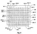
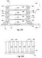
- an IC device stack assembly 10includes a stack of integrated circuit semiconductor devices 14 A, 14 B, 14 C, and 14 D (collectively referred to as ICs 14 ) positioned on a board 18 .
- ICs 14are illustrated as Thin Small-Outline Package (TSOP) devices, but may have another packaging or be unpackaged.
- ICs 14may be any of a variety of devices including, but not limited to, dynamic random access memory (DRAM), static random access memory (SRAM), programmable read only memory (PROM), application specific integrated circuits (ASICs), gate arrays, control devices, and microprocessors.
- DRAMdynamic random access memory
- SRAMstatic random access memory
- PROMprogrammable read only memory
- ASICsapplication specific integrated circuits
- gate arrayscontrol devices, and microprocessors.
- the inventionmay be used with a dual-in-line package stack on a dual-in-line board.
- Board 18may be any of a variety of boards or supports including, but not limited to, a PCB. Although four integrated circuit semiconductor devices are shown in the IC device stack assembly 10 of ICs, the IC device stack assembly 10 could include a greater or lesser number.
- Individual integrated circuit semiconductor devices 14 A and 14 Bmay be adhered to each other through adhesive 22 A. Accordingly, individual integrated circuit semiconductor devices 14 B and 14 C may be adhered to each other through adhesive 22 B. Similarly, integrated circuit semiconductor devices 14 C and 14 D may be adhered to each other through adhesive 22 C while integrated circuit semiconductor device 14 D may be adhered to board 18 through adhesive 22 D.
- Adhesives 22 A, 22 B, 22 C, and 22 D(referred to collectively as adhesives 22 ) may be an adhesively coated tape or a suitable type liquid adhesive. If desired, adhesive 22 D may differ from adhesives 22 A, 22 B, and 22 C. Structural members (not shown) other than adhesive may be used to position the ICs 14 with respect to each other, if desired.
- ICs 14include terminals 30 A, 30 B, 30 C, and 30 D (collectively terminals 30 ) and terminals 32 A, 32 B, 32 C, and 32 D (collectively terminals 32 ) to interface with external electrical components.
- Terminals 30 and 32are illustrated as cropped lead fingers, but could have a variety of other desired shapes.
- Multiconductor ports 36 and 38described below, are supported by board 18 .
- terminals 30 Ainclude terminals 30 A- 1 , 30 A- 2 , 30 A- 3 , 30 A- 4 , 30 A- 5 , 30 A- 6 , 30 A- 7 , 30 A- 8 , 30 A- 9 , 30 A- 10 , and 30 A- 11 .
- terminalsmay be applied to more than two sides of ICs 14 .
- terminals like terminals 30 and 32could be applied to all four sides of each individual IC device 14 .
- multiconductor insulating assembliesare connected between terminals 30 and multiconductor port 36 and between terminals 32 and multiconductor port 38 .
- the multiconductor insulating assembliesinclude multiconductors, as well as insulating material therebetween to separate conductors.
- the insulating materialmay provide a pliable, flexible, yet supportive structure to the conductors.
- the insulating materialmay be any of various materials including, but not limited to, tape and epoxy.
- the tapemay be a polyamide resin in the form of a film (such as is marketed by duPont under the name KaptonTM).
- KaptonTMThe tape may also be a well known type of heat sensitive shrink type tape.
- the conductive materialsmay be any of a variety of materials including copper wire, electrically conductive epoxy, such as EPO-TEK H37-MP silver filled epoxy, sold by Epoxy Technology, Inc., Billerica, Mass. 01821-3972, or the like.
- multiconductor insulating assembly tape 42includes conductors (collectively conductors 50 (FIGS. 4 A, 4 B)) having conductive sections that interface with terminals 30 A, 30 B, 30 C, and 30 D, and with multiconductor port 36 .
- the nature of these sectionsdepends on the structure and shape of such terminals, the structure of multiconductor port 36 , and means of keeping multiconductor insulating assembly tape 42 stationary with respect to the individual IC devices 14 A- 14 D and multiconductor port 36 .
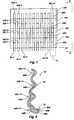
- multiconductor insulating assembly tape 42is referred to as Y-axis tape, because it includes straight conductors 50 applied to a tape backing 52 . Conductors 50 are aligned with a Y-axis with respect to an X-axis board 18 .
- Multiconductor insulating assembly tape 42may be wrapped about a spool 48 . As a portion of multiconductor insulating assembly tape 42 is unwound from spool 48 , it may be applied to the side of the stacked ICs 14 , individually, 14 A- 14 D as shown in FIG. 3 .
- conductors 50For ease in understanding, a portion of conductors 50 have been labeled 50 - 1 , 50 - 2 , 50 - 3 , 50 - 4 , . . . , and 50 - 11 . Conductors 50 are spaced apart from one another so as to align with respective ones of terminals 30 A, respective ones of terminals 30 B, respective ones of terminals 30 C, and respective ones of terminals 30 D.
- Tape backing 52preferably includes a suitable adhesive thereon so as to adhere to the side of ICs 14 , individually 14 A- 14 D. For example, as shown in FIG. 3 , a portion of backing 52 makes contact with a portion of each of the individual ICs 14 A- 14 D at points 56 , 58 , and 60 .
- FIG. 5shows conductors 50 - 1 , 50 - 2 , 50 - 3 , . . . , and 50 - 11 in alignment and making electrical contact with terminals 30 A- 1 , 30 A- 2 , 30 A- 3 , . . . , and 30 A- 1 1 ; and in alignment and making electrical contact with terminals 30 B- 1 , 30 B- 2 , 30 B- 3 , . . . , and 30 B- 11 ; in alignment and making electrical contact with terminals 30 C- 1 , 30 C- 2 , 30 C- 3 , and 30 C- 11 ; and in alignment and making electrical contact with terminals 30 D- 1 , 30 D- 2 , 30 D- 3 , . . . , and 30 D- 11 . (To avoid unnecessary clutter in the drawing figure, not all terminals and conductors are labeled.)
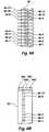
- FIG. 6Ashows a top view of multiconductor port 36 , which includes conductive sections 66 - 1 , 66 - 2 , 66 - 3 , . . . , and 66 - 11 spaced to align with conductors 50 - 1 , 50 - 2 , 50 - 3 , . . . , and 50 - 11 , respectively.
- Multiconductor insulating assembly tape 44may be substantially the same as or somewhat different from multiconductor insulating assembly tape 42 , and terminals 32 A, 32 B, 32 C, and 32 D may be substantially the same as or somewhat different from terminals 30 A, 30 B, 30 C, and 30 D. Further, multiconductor port 38 may be substantially the same as or somewhat different from multiconductor port 36 .
- Multiconductor insulating assembly tape 42may be cut after conductor 50 - 11 , or it may just be applied to an adjacent assembly (similar to assembly 10 ) or wrapped around the back of IC device stack assembly 10 and applied to terminals 32 A- 32 D.
- terminals 30 A- 11 , 30 B- 11 , 30 C- 11 , and 30 D- 11could be used as enabling terminals.
- multiconductor insulating assembly tape 42could be cut after conductor 50 - 10 and four separate conductors 68 A, 68 B, 68 C, and 68 D could be applied to terminals 30 A- 11 , 30 B- 11 , 30 C- 11 , and 30 D- 11 , respectively.
- separate conductors 68 A, 68 B, 68 C, and 68 Dcould be joined in a tape 70 ( FIG. 8 ) with an adhesive backing strip 74 thereon (the borders of which are shown in dashed lines).
- conductor 68 Dwould be immediately adjacent to conductor 68 C, which would be immediately adjacent to conductor 68 B, which would be immediately adjacent to conductor 68 A, for the portion of tape 70 below the respective terminal.
- conductors 68 B, 68 C, and 68 DThere is an insulating coating of conductors 68 B, 68 C, and 68 D, or other insulation means between conductors. (For purposes of illustration, the relative widths of conductors 68 and tape 70 are exaggerated.)
- conductors 68 A, 68 B, 68 C, and 68 Dcould traverse different portions of adhesive backing 74 so as not to require overlap.
- conductors 68 A, 68 B, 68 C, and 68 Dcould be completely separate, each having a different backing, or be surrounded by insulators.
- the terminals that control chip enablecould be on another portion of the ICs 14 , such as on the front or back (whereas terminals 30 and 32 are on the side).
- more than one enable terminalwould be required. Enablement could be controlled by addressing signals (e.g., the 2 or 3 most significant bits). Further, more than merely enable terminals could be different from each individual integrated circuit semiconductor device, such as IC 14 A, as compared to another individual integrated circuit semiconductor device, such as IC 14 B. In such an example, various possible multiconductor insulating assemblies may be used including those illustrated in FIGS. 8, 9 , and 10 . It is possible to have a single multiconductor insulating assembly tape with different levels of conductors for different terminals.
- FIG. 10illustrates four separate conductors being used as an alternative to that of FIG. 9 .
- FIG. 6Billustrates an alternative multiconductor port 36 with four conductive sections 76 A, 76 B, 76 C, and 76 D which may be used in connection with the devices of FIGS. 8, 9 , and 10 .
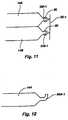
- interface between terminals 30 and conductors 50could be made with a male-female relationship.
- female members 80could be connected to conductors 50 - 1 through 50 - 11 .
- the terminalsmay have a variety of shapes. For example, by curving terminal 90 A- 1 (rather than terminal 30 A- 1 ), there is more surface to contact a conductor.
- a multiconductor epoxy assembly 102 and a multistrand insulating epoxy assembly 104are used in an IC device stack assembly 108 , which may be the same as IC device stack assembly 10 except for replacing multiconductor insulating tape 42 with multiconductor and insulating epoxy assemblies 102 and 104 .
- multiconductor epoxy assembly 102includes a plurality of conductors 102 ′, each formed of suitable well known conductive epoxy material.
- Multistrand insulating epoxy assembly 104includes a plurality of strips of nonconductive epoxy material 114 located between the conductors 102 ′. Conductors 102 ′, like conductors 50 may be injected into, bombarded on, or otherwise adhered to the nonconductive epoxy material 114 forming multistrand insulating epoxy assembly 104 .
- the base epoxy material of multistrand insulating epoxy assembly 104may be substantially the same epoxy material as or somewhat different from the base epoxy material of multiconductor epoxy assembly 102 .
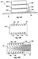
- FIG. 14Aa stack 130 of ICs that includes a stack of unpackaged ICs 132 A, 132 B, and 132 C is illustrated.
- the bottom of each of the ICs 132 A, 132 B, and 132 C(of which device 132 A is representative) includes bonding pads 134 thereon (which are a form of terminals).
- the top of multiconductor insulating assembly tape 136 A, 136 B, and 136 C(of which tape 136 A is representative) includes corresponding contact pads 138 connected to conductors 140 .
- Conductors 140make electrical contact with a multiconductor port 142 to interface with other external circuitry.
- the bonding padsmay be located on the top of each of the individual ICs.
- One integrated multiconductor/insulating tape assemblymay service IC devices on the top and bottom of the tape.
- a plurality of conductors 50 - 1 ′, 50 - 2 ′, 50 - 3 ′, 50 - 4 ′, 50 - 5 ′, etc.may be formed in an extrusion of suitable insulating material 160 .
- Any desired number of conductors 50 - 1 ′, etc.may be formed in the extrusion in any desired matrix configuration.
- the conductors 50 - 1 ′, etc.may be any desired shape, such as square, rectangular, etc.
- the matrix configurationmay be of any desired shape, such as square, rectangular, etc.
- the plurality of conductors 50 - 1 ′, etc. in the insulating material 160 as illustrated in drawing FIG. 15is shown in an end view to illustrate the conductors 50 - 1 ′, etc. formed within the insulating material 160 to form the desired matrix of conductors.
- the conductor matrixmay be any desired shape having any desired number of conductors 50 - 1 ′, etc. arranged therein.
- the conductor matrixmay be cut along either lines A-A or B-B to expose a plurality of conductors 50 - 1 ′, etc. to form a multiconductor flexible insulating assembly for connection to a plurality of ICs 14 .
- the insulating material 160may be adhesively bonded or secured to portions of the ICs 14 , as described previously herein, while the conductors 50 - 1 ′, etc. may be secured in any suitable manner to the terminals 30 A- 1 , etc. of the ICs 14 , as described herein, to connect the multiconductor flexible insulating assembly to the ICs 14 .
- the conductors 50 - 1 ′, etc.may be conveniently extruded in a suitable insulation material matrix and cut to the desired number and length to form the desired multiconductor flexible insulating assembly before connection to the terminals 30 A- 1 , etc. of the ICs 14 .
- LOCLOC, TAB, and flip-chip arrangements may be used in connection with the various embodiments of the present invention.
- connectionand related words are used in an operational sense, and are not necessarily limited to a direct connection.
- terminals 30are connected to multiconductor port 36 , but indirectly through a conductor of a multiconductor insulating assembly tape or epoxy.
Landscapes
- Engineering & Computer Science (AREA)
- Power Engineering (AREA)
- Microelectronics & Electronic Packaging (AREA)
- Physics & Mathematics (AREA)
- Condensed Matter Physics & Semiconductors (AREA)
- General Physics & Mathematics (AREA)
- Computer Hardware Design (AREA)
- Wire Bonding (AREA)
Abstract
Description
- This application is a continuation of application Ser. No. 10/634,073, filed Aug. 4, 2003, pending, which is a continuation of application Ser. No. 10/154,549, filed May 24, 2002, now U.S. Pat. No. 6,656,767, issued Dec. 2, 2003, which is a continuation of application Ser. No. 09/923,481, filed Aug. 6, 2001, now U.S. Pat. No. 6,465,275, issued Oct. 15, 2002, which is a continuation of application Ser. No. 09/641,574, filed Aug. 18, 2000, now U.S. Pat. No. 6,329,221, issued Dec. 11, 2001, which is a continuation of application Ser. No. 09/036,662, filed Mar. 9, 1998, now U.S. Pat. No. 6,207,474, issued Mar. 27, 2001.
- 1. Field of the Invention
- The invention relates to packaged integrated circuit devices. More specifically, the present invention relates to an interconnected stack of packaged memory devices and the method of forming a stack of interconnected packaged memory devices.
- 2. State of the Art
- High performance, low cost, increased miniaturization of components, and greater packaging density of integrated circuit semiconductor devices (ICs) have long been the goals of the computer industry. Greater integrated circuit semiconductor device package density for a given level of component and internal conductor density is primarily limited by the space available for die mounting and packaging. For lead frame mounted dice, this limitation is, to a great extent, a result of lead frame design.
- In a conventional lead frame design, the lead frame includes a plurality of leads having their ends terminating adjacent a side or edge of an integrated circuit semiconductor device supported by the die paddle portion of the lead frame. Electrical connections are made by means of wire bonds extending between the leads of the lead frame and the bond pads located on the active surface of the integrated circuit semiconductor device. Subsequent to the wire bonding operation, portions of the leads of the lead frame and the integrated circuit semiconductor device are encapsulated in suitable plastic material to form a packaged semiconductor device. The leads and lead frame are then trimmed and formed to the desired configuration after the packaging of the semiconductor device in the encapsulant material.
- In a Leads-Over-Chip (LOC) type lead frame configuration for an integrated circuit semiconductor (IC) device, the leads of the lead frame extend over the active surface of the semiconductor device being insulated therefrom by tape which is adhesively bonded to the semiconductor device and the leads of the lead frame. Electrical connections are made between the leads of the lead frame and bond pads on the active surface of the semiconductor device by way of wire bonds extending therebetween. After wire bonding, the leads of the LOC lead frame and the semiconductor device are encapsulated in suitable plastic to encapsulate the semiconductor device and portions of the leads. Subsequently, the leads are trimmed and formed to the desired configuration to complete the packaged semiconductor device.
- With ever-increasing demands for miniaturization and higher operating speeds, multichip module systems (MCMs) have become increasingly attractive in a variety of applications. Generally, MCMs may be designed to include more than one type of semiconductor device within a single package, or may include multiples of the same type of semiconductor device, such as the single-in-line memory module (SIMM) or dual-in-line memory module (DIMM).
- MCMs typically comprise a planar printed circuit board (PCB) or other semiconductor carrier substrate to which a plurality of semiconductor devices is attached. Laminated substrates, such as FR-4 boards, are included in the term PCB as used herein, as are ceramic and silicon substrates, although the latter constructions are at this time less common as MCM carrier substrates. The semiconductor devices are typically wire bonded, TAB-connected or flip-chip bonded (by an array of solder or other conductive bumps or conductive epoxies) to the PCB. An MCM configuration typically allows semiconductor devices to be bonded to one side only of the carrier substrate. Moreover, for semiconductor devices that are wire bonded to the PCB, the bond wires extend from the top surface of each semiconductor device mounted on one side of the PCB by its back side to the plane of the PCB surface on the back side, requiring longer wires to be used to connect the semiconductor devices to the PCB traces than if the active surface of the semiconductor device were closer to the PCB surface. This often leads to undesirable parasitic electrical characteristics. Also, mounting the semiconductor devices on a substrate to be subsequently mounted on the PCB uses valuable area of the PCB which may be used for other purposes. Additionally, the plurality of wires used to connect the semiconductor devices to the substrate of the MCM affects the speed at which the MCM responds when connected to the PCB. In many instances, PCBs (such as those used in computers) have fixed size requirements, thereby making space on the PCB scarce. Therefore, a need exists for a high density, minimal volume configuration, and high response rate series of interconnected semiconductor devices for use in conjunction with a PCB.
- An integrated circuit semiconductor device stack includes a stack of packaged integrated circuit semiconductor devices (ICs) supported by a board or other support surface. One or more multiconductor insulating assembly provides an interface between terminals of the ICs and external circuitry. One embodiment of the multiconductor insulating assembly includes tape (such as Kapton™ tape) on which conductors are applied. One surface of the tape is preferably adhesive so as to stick to the ICs. When properly aligned, the conductors make contact with the terminals of the ICs and with a multiconductor port. There may be multiple layers of conductors where different terminals of individual ICs aligned in a stack are to receive different signals. Another embodiment of the multiconductor insulating assembly includes an epoxy onto which conductors are applied. In yet another embodiment, multiconductor insulating assembly tape is sandwiched between ICs. Contact pads on the tape are aligned with bonding pads on the ICs. In yet another embodiment of the multiconductor insulating assembly, multiple conductors are extruded and cut to form the desired multiconductor assembly which is subsequently adhesively bonded to the ICs with the conductors in contact with the bonding pads on the ICs.
- While the specification concludes with claims particularly pointing out and distinctly claiming that which is regarded as the present invention, the advantages of this invention can be more readily ascertained from the following description of the invention when read in conjunction with the accompanying drawings in which:
FIG. 1 is a front view of a stack of ICs on a board;FIG. 2 is a side view of one of the ICs taken along lines2-2 ofFIG. 1 ;FIG. 3 is a front view of a stack of ICs according to one embodiment of the present invention;FIG. 4A is a side view of a spool of tape used in connection withFIG. 3 ;FIG. 4B is a top view of the tape ofFIG. 4A ;FIG. 5 is a side view of a portion ofFIG. 1 ;FIG. 6A is a top view of a multiconductor port ofFIG. 1 ;FIG. 6B is a top view of an alternative multiconductor port;FIG. 7 is an alternative embodiment to that ofFIG. 5 ;FIG. 8 is a cross-sectional view taken along line8-8 ofFIG. 7 ;FIG. 9 is a front view of an alternative multiconductor insulating assembly tape;FIG. 10 is a front view of four separate conductors connected to four terminals;FIG. 11 is a front view of alternative means of connection between terminals and a multiconductor insulating assembly tape;FIG. 12 is an alternative shape for a terminal;FIG. 13A is a front view of an alternative embodiment of the present invention of a stack of ICs using a conductive epoxy;FIG. 13B is a side view along line B-B ofFIG. 13A of the present invention;FIG. 14A is a front view of yet another embodiment of the present invention of a stack of ICs;FIG. 14B is a bottom view of one of the ICs ofFIG. 14A ;FIG. 14C is a top view of one of the multiconductor insulating assembly tapes ofFIG. 14A ;FIG. 15 is a side view of a multiconductor extrusion prior to cutting a multiconductor insulating assembly therefrom; andFIG. 16 is an end view of the multiconductor extrusion ofFIG. 15 prior to cutting a multiconductor insulating assembly therefrom.- Referring to
FIG. 1 , an ICdevice stack assembly 10 includes a stack of integratedcircuit semiconductor devices board 18. ICs14 are illustrated as Thin Small-Outline Package (TSOP) devices, but may have another packaging or be unpackaged. ICs14 may be any of a variety of devices including, but not limited to, dynamic random access memory (DRAM), static random access memory (SRAM), programmable read only memory (PROM), application specific integrated circuits (ASICs), gate arrays, control devices, and microprocessors. Merely as an example, and not a limitation, the invention may be used with a dual-in-line package stack on a dual-in-line board.Board 18 may be any of a variety of boards or supports including, but not limited to, a PCB. Although four integrated circuit semiconductor devices are shown in the ICdevice stack assembly 10 of ICs, the ICdevice stack assembly 10 could include a greater or lesser number. - Individual integrated
circuit semiconductor devices circuit semiconductor devices circuit semiconductor devices circuit semiconductor device 14D may be adhered to board18 through adhesive22D.Adhesives adhesives - ICs14 include
terminals terminals Multiconductor ports board 18. - Referring to
FIG. 2 , a side view ofterminals 30A taken along lines2-2 ofFIG. 1 is representative of side views ofterminals terminals Terminals 30A includeterminals 30A-1,30A-2,30A-3,30A-4,30A-5,30A-6,30A-7,30A-8,30A-9,30A-10, and30A-11. Of course, a greater or lesser number of terminals may be employed in a particular example. Further, terminals may be applied to more than two sides of ICs14. For example, terminals like terminals30 and32 could be applied to all four sides of each individual IC device14. - To facilitate the interface between ICs14 and external electrical components, multiconductor insulating assemblies are connected between terminals30 and
multiconductor port 36 and between terminals32 andmulticonductor port 38. The multiconductor insulating assemblies include multiconductors, as well as insulating material therebetween to separate conductors. The insulating material may provide a pliable, flexible, yet supportive structure to the conductors. The insulating material may be any of various materials including, but not limited to, tape and epoxy. The tape may be a polyamide resin in the form of a film (such as is marketed by duPont under the name Kapton™). The tape may also be a well known type of heat sensitive shrink type tape. The conductive materials may be any of a variety of materials including copper wire, electrically conductive epoxy, such as EPO-TEK H37-MP silver filled epoxy, sold by Epoxy Technology, Inc., Billerica, Mass. 01821-3972, or the like. - Referring to
FIG. 3 , multiconductor insulatingassembly tape 42 includes conductors (collectively conductors50 (FIGS.4A,4B)) having conductive sections that interface withterminals multiconductor port 36. The nature of these sections depends on the structure and shape of such terminals, the structure ofmulticonductor port 36, and means of keeping multiconductor insulatingassembly tape 42 stationary with respect to theindividual IC devices 14A-14D andmulticonductor port 36. - For example, referring to
FIGS. 4A and 4B , multiconductor insulatingassembly tape 42 is referred to as Y-axis tape, because it includes straight conductors50 applied to atape backing 52. Conductors50 are aligned with a Y-axis with respect to anX-axis board 18. Multiconductor insulatingassembly tape 42 may be wrapped about aspool 48. As a portion of multiconductorinsulating assembly tape 42 is unwound fromspool 48, it may be applied to the side of the stacked ICs14, individually,14A-14D as shown inFIG. 3 . For ease in understanding, a portion of conductors50 have been labeled50-1,50-2,50-3,50-4, . . . , and50-11. Conductors50 are spaced apart from one another so as to align with respective ones ofterminals 30A, respective ones ofterminals 30B, respective ones ofterminals 30C, and respective ones ofterminals 30D. Tape backing 52 preferably includes a suitable adhesive thereon so as to adhere to the side of ICs14, individually14A-14D. For example, as shown inFIG. 3 , a portion of backing52 makes contact with a portion of each of theindividual ICs 14A-14D at points56,58, and60.- For example, FIG.5 shows conductors50-1,50-2,50-3, . . . , and50-11 in alignment and making electrical contact with
terminals 30A-1,30A-2,30A-3, . . . , and30A-11; and in alignment and making electrical contact withterminals 30B-1,30B-2,30B-3, . . . , and30B-11; in alignment and making electrical contact withterminals 30C-1,30C-2,30C-3, and30C-11; and in alignment and making electrical contact withterminals 30D-1,30D-2,30D-3, . . . , and30D-11. (To avoid unnecessary clutter in the drawing figure, not all terminals and conductors are labeled.) FIG. 6A shows a top view ofmulticonductor port 36, which includes conductive sections66-1,66-2,66-3, . . . , and66-11 spaced to align with conductors50-1,50-2,50-3, . . . , and50-11, respectively.- Multiconductor insulating
assembly tape 44 may be substantially the same as or somewhat different from multiconductor insulatingassembly tape 42, andterminals terminals multiconductor port 38 may be substantially the same as or somewhat different frommulticonductor port 36. - Multiconductor insulating
assembly tape 42 may be cut after conductor50-11, or it may just be applied to an adjacent assembly (similar to assembly10) or wrapped around the back of ICdevice stack assembly 10 and applied toterminals 32A-32D. - In most situations, it is not desirable that every terminal on each IC device14 receive exactly the same electrical signal. Accordingly, it is desirable that some terminals on
IC devices 14A-14D receive different signals. Merely as an example, for each of theindividual ICs 14A-14D,terminals 30A-11,30B-11,30C-11, and30D-11 could be used as enabling terminals. - Referring to
FIG. 7 , in such a case, merely as an example, multiconductor insulatingassembly tape 42 could be cut after conductor50-10 and fourseparate conductors terminals 30A-11,30B-11,30C-11, and30D-11, respectively. Merely as an example,separate conductors FIG. 8 ) with anadhesive backing strip 74 thereon (the borders of which are shown in dashed lines). - Merely as one example, as illustrated in
FIG. 8 (which is a side view taken along lines8-8 ofFIG. 7 ),conductor 68D would be immediately adjacent toconductor 68C, which would be immediately adjacent toconductor 68B, which would be immediately adjacent toconductor 68A, for the portion oftape 70 below the respective terminal. There is an insulating coating ofconductors tape 70 are exaggerated.) - As another example, as shown in
FIG. 9 ,conductors adhesive backing 74 so as not to require overlap. As still another option,conductors FIGS. 8, 9 , or10, the terminals that control chip enable could be on another portion of the ICs14, such as on the front or back (whereas terminals30 and32 are on the side). - In some cases, more than one enable terminal would be required. Enablement could be controlled by addressing signals (e.g., the 2 or 3 most significant bits). Further, more than merely enable terminals could be different from each individual integrated circuit semiconductor device, such as
IC 14A, as compared to another individual integrated circuit semiconductor device, such asIC 14B. In such an example, various possible multiconductor insulating assemblies may be used including those illustrated inFIGS. 8, 9 , and10. It is possible to have a single multiconductor insulating assembly tape with different levels of conductors for different terminals. For example, when all corresponding terminals ofICs 14A-14D (e.g.,terminals 30A-2,30B-2,30C-2, and30D-2) are to receive the same signal, there need be only one level of conductor. By contrast, if the corresponding terminals ofICs 14A-14D (e.g.,terminals 30A-2,30B-2,30C-2, and30D-2) are each to receive different signals, then four levels of conductors may be used.FIG. 10 illustrates four separate conductors being used as an alternative to that ofFIG. 9 . FIG. 6B illustrates an alternativemulticonductor port 36 with fourconductive sections FIGS. 8, 9 , and10.- Referring to
FIG. 11 , interface between terminals30 and conductors50 could be made with a male-female relationship. For example,female members 80 could be connected to conductors50-1 through50-11. - Referring to
FIG. 12 , the terminals may have a variety of shapes. For example, by curving terminal90A-1 (rather than terminal30A-1), there is more surface to contact a conductor. - Referring to
FIG. 13A , a multiconductorepoxy assembly 102 and a multistrand insulatingepoxy assembly 104 are used in an ICdevice stack assembly 108, which may be the same as ICdevice stack assembly 10 except for replacing multiconductorinsulating tape 42 with multiconductor and insulatingepoxy assemblies - Referring to drawing
FIG. 13B , multiconductorepoxy assembly 102 includes a plurality ofconductors 102′, each formed of suitable well known conductive epoxy material. Multistrand insulatingepoxy assembly 104 includes a plurality of strips of nonconductiveepoxy material 114 located between theconductors 102′.Conductors 102′, like conductors50 may be injected into, bombarded on, or otherwise adhered to the nonconductiveepoxy material 114 forming multistrand insulatingepoxy assembly 104. Multiple layers of conductors may also be applied to or into nonconductiveepoxy material 114, such as is the case where corresponding terminals (e.g.,terminals 30A-2,30B-2,30C-2, and30D-2) are not to receive the same signal. The base epoxy material of multistrand insulatingepoxy assembly 104 may be substantially the same epoxy material as or somewhat different from the base epoxy material of multiconductorepoxy assembly 102. - Referring to drawing
FIG. 14A , astack 130 of ICs that includes a stack ofunpackaged ICs FIGS. 14A and 14B , the bottom of each of theICs device 132A is representative) includesbonding pads 134 thereon (which are a form of terminals). As shown inFIGS. 14A-14C , the top of multiconductorinsulating assembly tape corresponding contact pads 138 connected toconductors 140.Conductors 140 make electrical contact with amulticonductor port 142 to interface with other external circuitry. As an alternative embodiment of the present invention to the embodiment shown inFIGS. 14A-14C , the bonding pads may be located on the top of each of the individual ICs. One integrated multiconductor/insulating tape assembly may service IC devices on the top and bottom of the tape. - Referring to drawing
FIG. 15 , in yet another embodiment of the invention, as shown in a side view, a plurality of conductors50-1′,50-2′,50-3′,50-4′,50-5′, etc. may be formed in an extrusion of suitable insulatingmaterial 160. Any desired number of conductors50-1′, etc. may be formed in the extrusion in any desired matrix configuration. The conductors50-1′, etc. may be any desired shape, such as square, rectangular, etc. The matrix configuration may be of any desired shape, such as square, rectangular, etc. - Referring to drawing
FIG. 16 , the plurality of conductors50-1′, etc. in the insulatingmaterial 160 as illustrated in drawingFIG. 15 is shown in an end view to illustrate the conductors50-1′, etc. formed within the insulatingmaterial 160 to form the desired matrix of conductors. The conductor matrix may be any desired shape having any desired number of conductors50-1′, etc. arranged therein. The conductor matrix may be cut along either lines A-A or B-B to expose a plurality of conductors50-1′, etc. to form a multiconductor flexible insulating assembly for connection to a plurality of ICs14. The insulatingmaterial 160 may be adhesively bonded or secured to portions of the ICs14, as described previously herein, while the conductors50-1′, etc. may be secured in any suitable manner to theterminals 30A-1, etc. of the ICs14, as described herein, to connect the multiconductor flexible insulating assembly to the ICs14. In this manner, the conductors50-1′, etc. may be conveniently extruded in a suitable insulation material matrix and cut to the desired number and length to form the desired multiconductor flexible insulating assembly before connection to theterminals 30A-1, etc. of the ICs14. - LOC, TAB, and flip-chip arrangements may be used in connection with the various embodiments of the present invention.
- As used herein, the term “connect” and related words are used in an operational sense, and are not necessarily limited to a direct connection. For example, terminals30 are connected to
multiconductor port 36, but indirectly through a conductor of a multiconductor insulating assembly tape or epoxy. - Having thus described in detail preferred embodiments of the present invention, it is to be understood that the invention defined by the appended claims is not to be limited by particular details set forth in the above description, as many apparent variations thereof are possible without departing from the spirit or scope thereof.
Claims (13)
Priority Applications (2)
| Application Number | Priority Date | Filing Date | Title |
|---|---|---|---|
| US11/092,348US7091061B2 (en) | 1998-03-09 | 2005-03-29 | Method of forming a stack of packaged memory dice |
| US11/482,667US20060252181A1 (en) | 1998-03-09 | 2006-07-06 | Method of forming a stack of packaged memory dice |
Applications Claiming Priority (6)
| Application Number | Priority Date | Filing Date | Title |
|---|---|---|---|
| US09/036,662US6207474B1 (en) | 1998-03-09 | 1998-03-09 | Method of forming a stack of packaged memory die and resulting apparatus |
| US09/641,574US6329221B1 (en) | 1998-03-09 | 2000-08-18 | Method of forming a stack of packaged memory die and resulting apparatus |
| US09/923,481US6465275B2 (en) | 1998-03-09 | 2001-08-06 | Method of forming a stack of packaged memory die and resulting apparatus |
| US10/154,549US6656767B1 (en) | 1998-03-09 | 2002-05-24 | Method of forming a stack of packaged memory dice |
| US10/634,073US6884654B2 (en) | 1998-03-09 | 2003-08-04 | Method of forming a stack of packaged memory dice |
| US11/092,348US7091061B2 (en) | 1998-03-09 | 2005-03-29 | Method of forming a stack of packaged memory dice |
Related Parent Applications (1)
| Application Number | Title | Priority Date | Filing Date |
|---|---|---|---|
| US10/634,073ContinuationUS6884654B2 (en) | 1998-03-09 | 2003-08-04 | Method of forming a stack of packaged memory dice |
Related Child Applications (1)
| Application Number | Title | Priority Date | Filing Date |
|---|---|---|---|
| US11/482,667ContinuationUS20060252181A1 (en) | 1998-03-09 | 2006-07-06 | Method of forming a stack of packaged memory dice |
Publications (2)
| Publication Number | Publication Date |
|---|---|
| US20050170558A1true US20050170558A1 (en) | 2005-08-04 |
| US7091061B2 US7091061B2 (en) | 2006-08-15 |
Family
ID=21889919
Family Applications (10)
| Application Number | Title | Priority Date | Filing Date |
|---|---|---|---|
| US09/036,662Expired - LifetimeUS6207474B1 (en) | 1998-03-09 | 1998-03-09 | Method of forming a stack of packaged memory die and resulting apparatus |
| US09/420,672Expired - LifetimeUS6445063B1 (en) | 1998-03-09 | 1999-10-19 | Method of forming a stack of packaged memory die and resulting apparatus |
| US09/641,574Expired - Fee RelatedUS6329221B1 (en) | 1998-03-09 | 2000-08-18 | Method of forming a stack of packaged memory die and resulting apparatus |
| US09/923,481Expired - LifetimeUS6465275B2 (en) | 1998-03-09 | 2001-08-06 | Method of forming a stack of packaged memory die and resulting apparatus |
| US10/121,851Expired - Fee RelatedUS6677671B2 (en) | 1998-03-09 | 2002-04-11 | Apparatus for forming a stack of packaged memory dice |
| US10/154,549Expired - LifetimeUS6656767B1 (en) | 1998-03-09 | 2002-05-24 | Method of forming a stack of packaged memory dice |
| US10/633,925Expired - LifetimeUS6897553B2 (en) | 1998-03-09 | 2003-08-04 | Apparatus for forming a stack of packaged memory dice |
| US10/634,073Expired - LifetimeUS6884654B2 (en) | 1998-03-09 | 2003-08-04 | Method of forming a stack of packaged memory dice |
| US11/092,348Expired - Fee RelatedUS7091061B2 (en) | 1998-03-09 | 2005-03-29 | Method of forming a stack of packaged memory dice |
| US11/482,667AbandonedUS20060252181A1 (en) | 1998-03-09 | 2006-07-06 | Method of forming a stack of packaged memory dice |
Family Applications Before (8)
| Application Number | Title | Priority Date | Filing Date |
|---|---|---|---|
| US09/036,662Expired - LifetimeUS6207474B1 (en) | 1998-03-09 | 1998-03-09 | Method of forming a stack of packaged memory die and resulting apparatus |
| US09/420,672Expired - LifetimeUS6445063B1 (en) | 1998-03-09 | 1999-10-19 | Method of forming a stack of packaged memory die and resulting apparatus |
| US09/641,574Expired - Fee RelatedUS6329221B1 (en) | 1998-03-09 | 2000-08-18 | Method of forming a stack of packaged memory die and resulting apparatus |
| US09/923,481Expired - LifetimeUS6465275B2 (en) | 1998-03-09 | 2001-08-06 | Method of forming a stack of packaged memory die and resulting apparatus |
| US10/121,851Expired - Fee RelatedUS6677671B2 (en) | 1998-03-09 | 2002-04-11 | Apparatus for forming a stack of packaged memory dice |
| US10/154,549Expired - LifetimeUS6656767B1 (en) | 1998-03-09 | 2002-05-24 | Method of forming a stack of packaged memory dice |
| US10/633,925Expired - LifetimeUS6897553B2 (en) | 1998-03-09 | 2003-08-04 | Apparatus for forming a stack of packaged memory dice |
| US10/634,073Expired - LifetimeUS6884654B2 (en) | 1998-03-09 | 2003-08-04 | Method of forming a stack of packaged memory dice |
Family Applications After (1)
| Application Number | Title | Priority Date | Filing Date |
|---|---|---|---|
| US11/482,667AbandonedUS20060252181A1 (en) | 1998-03-09 | 2006-07-06 | Method of forming a stack of packaged memory dice |
Country Status (1)
| Country | Link |
|---|---|
| US (10) | US6207474B1 (en) |
Cited By (2)
| Publication number | Priority date | Publication date | Assignee | Title |
|---|---|---|---|---|
| TWI395305B (en)* | 2005-09-02 | 2013-05-01 | Semiconductor Energy Lab | Integrated circuit device |
| US8981574B2 (en) | 2012-12-20 | 2015-03-17 | Samsung Electronics Co., Ltd. | Semiconductor package |
Families Citing this family (67)
| Publication number | Priority date | Publication date | Assignee | Title |
|---|---|---|---|---|
| US6207474B1 (en)* | 1998-03-09 | 2001-03-27 | Micron Technology, Inc. | Method of forming a stack of packaged memory die and resulting apparatus |
| US6147411A (en)* | 1998-03-31 | 2000-11-14 | Micron Technology, Inc. | Vertical surface mount package utilizing a back-to-back semiconductor device module |
| US6900549B2 (en)* | 2001-01-17 | 2005-05-31 | Micron Technology, Inc. | Semiconductor assembly without adhesive fillets |
| US6618257B1 (en)* | 2001-07-27 | 2003-09-09 | Staktek Group, L.P. | Wide data path stacking system and method |
| JP2003133518A (en)* | 2001-10-29 | 2003-05-09 | Mitsubishi Electric Corp | Semiconductor module |
| US7332819B2 (en)* | 2002-01-09 | 2008-02-19 | Micron Technology, Inc. | Stacked die in die BGA package |
| US6958533B2 (en)* | 2002-01-22 | 2005-10-25 | Honeywell International Inc. | High density 3-D integrated circuit package |
| US6690088B2 (en)* | 2002-01-31 | 2004-02-10 | Macintyre Donald M. | Integrated circuit package stacking structure |
| US6979904B2 (en)* | 2002-04-19 | 2005-12-27 | Micron Technology, Inc. | Integrated circuit package having reduced interconnects |
| KR100442880B1 (en)* | 2002-07-24 | 2004-08-02 | 삼성전자주식회사 | Stacked semiconductor module and manufacturing method thereof |
| US6700206B2 (en) | 2002-08-02 | 2004-03-02 | Micron Technology, Inc. | Stacked semiconductor package and method producing same |
| US7959437B2 (en) | 2002-10-29 | 2011-06-14 | Rmo, Inc. | Orthodontic appliance with encoded information formed in the base |
| US7695277B1 (en) | 2004-10-28 | 2010-04-13 | Rmo, Inc. | Orthodontic bracket with frangible cover mechanism |
| KR20040066553A (en)* | 2003-01-20 | 2004-07-27 | 삼성전자주식회사 | Integrated monitoring burn in test method for Multi-chip Package |
| US7098541B2 (en)* | 2003-05-19 | 2006-08-29 | Hewlett-Packard Development Company, L.P. | Interconnect method for directly connected stacked integrated circuits |
| KR100506035B1 (en)* | 2003-08-22 | 2005-08-03 | 삼성전자주식회사 | Semiconductor package and manufacturing method thereof |
| US6953994B2 (en)* | 2003-10-02 | 2005-10-11 | Interdigital Technology Corporation | Wireless coupling of staked dies within system in package |
| DE102004030383A1 (en)* | 2004-06-23 | 2006-01-12 | Infineon Technologies Ag | Bonding film and semiconductor component with bonding film and method for their production |
| US7211510B2 (en)* | 2004-09-09 | 2007-05-01 | Advanced Bionics Corporation | Stacking circuit elements |
| US7217994B2 (en)* | 2004-12-01 | 2007-05-15 | Kyocera Wireless Corp. | Stack package for high density integrated circuits |
| US7151010B2 (en)* | 2004-12-01 | 2006-12-19 | Kyocera Wireless Corp. | Methods for assembling a stack package for high density integrated circuits |
| CN101138089B (en)* | 2005-01-31 | 2011-02-09 | 斯班逊有限公司 | Stacked semiconductor device and method for manufacturing stacked semiconductor device |
| US20070109756A1 (en)* | 2005-02-10 | 2007-05-17 | Stats Chippac Ltd. | Stacked integrated circuits package system |
| US7242091B2 (en)* | 2005-03-02 | 2007-07-10 | Stats Chippac Ltd. | Stacked semiconductor packages and method therefor |
| US7518224B2 (en)* | 2005-05-16 | 2009-04-14 | Stats Chippac Ltd. | Offset integrated circuit package-on-package stacking system |
| US7746656B2 (en)* | 2005-05-16 | 2010-06-29 | Stats Chippac Ltd. | Offset integrated circuit package-on-package stacking system |
| KR100690246B1 (en)* | 2006-01-10 | 2007-03-12 | 삼성전자주식회사 | Method of manufacturing a package that is a flip chip system |
| TWI322492B (en)* | 2006-05-30 | 2010-03-21 | Advanced Semiconductor Eng | Stacked semiconductor package having flexible circuit board therein |
| US7535086B2 (en)* | 2006-08-03 | 2009-05-19 | Stats Chippac Ltd. | Integrated circuit package-on-package stacking system |
| US7550318B2 (en)* | 2006-08-11 | 2009-06-23 | Freescale Semiconductor, Inc. | Interconnect for improved die to substrate electrical coupling |
| US7888185B2 (en)* | 2006-08-17 | 2011-02-15 | Micron Technology, Inc. | Semiconductor device assemblies and systems including at least one conductive pathway extending around a side of at least one semiconductor device |
| WO2008020810A1 (en)* | 2006-08-18 | 2008-02-21 | Wai Seng Chew | Edge bond chip connection (ebcc) |
| US9554875B2 (en) | 2006-09-07 | 2017-01-31 | Rmo, Inc. | Method for producing a customized orthodontic appliance |
| US8979528B2 (en) | 2006-09-07 | 2015-03-17 | Rmo, Inc. | Customized orthodontic appliance method and system |
| WO2008031060A2 (en) | 2006-09-07 | 2008-03-13 | Rmo, Inc. | Reduced-friction buccal tube and method of use |
| US7761624B2 (en)* | 2006-09-28 | 2010-07-20 | Virident Systems, Inc. | Systems and apparatus for main memory with non-volatile type memory modules, and related technologies |
| US7761626B2 (en)* | 2006-09-28 | 2010-07-20 | Virident Systems, Inc. | Methods for main memory in a system with a memory controller configured to control access to non-volatile memory, and related technologies |
| US8949555B1 (en) | 2007-08-30 | 2015-02-03 | Virident Systems, Inc. | Methods for sustained read and write performance with non-volatile memory |
| US7761625B2 (en)* | 2006-09-28 | 2010-07-20 | Virident Systems, Inc. | Methods for main memory with non-volatile type memory modules, and related technologies |
| US20080082750A1 (en)* | 2006-09-28 | 2008-04-03 | Okin Kenneth A | Methods of communicating to, memory modules in a memory channel |
| US9984012B2 (en) | 2006-09-28 | 2018-05-29 | Virident Systems, Llc | Read writeable randomly accessible non-volatile memory modules |
| US7761623B2 (en)* | 2006-09-28 | 2010-07-20 | Virident Systems, Inc. | Main memory in a system with a memory controller configured to control access to non-volatile memory, and related technologies |
| US8074022B2 (en)* | 2006-09-28 | 2011-12-06 | Virident Systems, Inc. | Programmable heterogeneous memory controllers for main memory with different memory modules |
| WO2008040028A2 (en)* | 2006-09-28 | 2008-04-03 | Virident Systems, Inc. | Systems, methods, and apparatus with programmable memory control for heterogeneous main memory |
| WO2008051940A2 (en)* | 2006-10-23 | 2008-05-02 | Virident Systems, Inc. | Methods and apparatus of dual inline memory modules for flash memory |
| KR100813626B1 (en)* | 2006-12-20 | 2008-03-14 | 삼성전자주식회사 | Stacked Semiconductor Device Package |
| US8163600B2 (en)* | 2006-12-28 | 2012-04-24 | Stats Chippac Ltd. | Bridge stack integrated circuit package-on-package system |
| FR2913128B1 (en)* | 2007-02-23 | 2009-08-28 | Total Immersion Sa | METHOD AND DEVICE FOR DETERMINING THE INSTALLATION OF A THREE-DIMENSIONAL OBJECT IN AN IMAGE AND METHOD AND DEVICE FOR CREATING AT LEAST ONE KEY IMAGE |
| JP5110996B2 (en)* | 2007-07-20 | 2012-12-26 | 新光電気工業株式会社 | Manufacturing method of stacked semiconductor device |
| US9921896B2 (en) | 2007-08-30 | 2018-03-20 | Virident Systems, Llc | Shutdowns and data recovery to avoid read errors weak pages in a non-volatile memory system |
| US8288860B2 (en)* | 2007-09-10 | 2012-10-16 | Stats Chippac Ltd. | Memory device system with stacked packages |
| US8856464B2 (en)* | 2008-02-12 | 2014-10-07 | Virident Systems, Inc. | Systems for two-dimensional main memory including memory modules with read-writeable non-volatile memory devices |
| WO2009102821A2 (en)* | 2008-02-12 | 2009-08-20 | Virident Systems, Inc. | Methods and apparatus for two-dimensional main memory |
| US8787060B2 (en) | 2010-11-03 | 2014-07-22 | Netlist, Inc. | Method and apparatus for optimizing driver load in a memory package |
| US8417873B1 (en) | 2008-06-24 | 2013-04-09 | Virident Systems, Inc. | Random read and read/write block accessible memory |
| US9513695B2 (en) | 2008-06-24 | 2016-12-06 | Virident Systems, Inc. | Methods of managing power in network computer systems |
| JP5700927B2 (en)* | 2008-11-28 | 2015-04-15 | 新光電気工業株式会社 | Semiconductor device and manufacturing method of semiconductor device |
| US11219507B2 (en) | 2009-03-16 | 2022-01-11 | Orthoamerica Holdings, Llc | Customized orthodontic appliance and method |
| WO2010107567A1 (en) | 2009-03-16 | 2010-09-23 | Rmo, Inc. | Orthodontic bracket having an archwire channel and archwire retaining mechanism |
| US9431375B2 (en) | 2011-04-01 | 2016-08-30 | Schlumberger Technology Corporation | High density microelectronics packaging |
| WO2012154190A1 (en) | 2011-05-12 | 2012-11-15 | Rmo, Inc. | Orthodontic appliance with encoded information formed in the base |
| USD660436S1 (en) | 2011-05-13 | 2012-05-22 | Rmo, Inc. | Orthodontic bracket |
| USD660968S1 (en) | 2011-05-13 | 2012-05-29 | Rmo, Inc. | Orthodontic bracket |
| USD660435S1 (en) | 2011-05-13 | 2012-05-22 | Rmo, Inc. | Orthodontic bracket |
| USD847349S1 (en) | 2011-09-22 | 2019-04-30 | Rmo, Inc. | Orthodontic lock with flange |
| USD726318S1 (en) | 2013-01-17 | 2015-04-07 | Rmo, Inc. | Dental instrument for a self-ligating orthodontic clip |
| USD721811S1 (en) | 2013-10-29 | 2015-01-27 | Rmo, Inc. | Orthodontic bracket |
Citations (45)
| Publication number | Priority date | Publication date | Assignee | Title |
|---|---|---|---|---|
| US4992849A (en)* | 1989-02-15 | 1991-02-12 | Micron Technology, Inc. | Directly bonded board multiple integrated circuit module |
| US4992850A (en)* | 1989-02-15 | 1991-02-12 | Micron Technology, Inc. | Directly bonded simm module |
| US4996587A (en)* | 1989-04-10 | 1991-02-26 | International Business Machines Corporation | Integrated semiconductor chip package |
| US5107328A (en)* | 1991-02-13 | 1992-04-21 | Micron Technology, Inc. | Packaging means for a semiconductor die having particular shelf structure |
| US5137836A (en)* | 1991-05-23 | 1992-08-11 | Atmel Corporation | Method of manufacturing a repairable multi-chip module |
| US5155067A (en)* | 1991-03-26 | 1992-10-13 | Micron Technology, Inc. | Packaging for a semiconductor die |
| US5239198A (en)* | 1989-09-06 | 1993-08-24 | Motorola, Inc. | Overmolded semiconductor device having solder ball and edge lead connective structure |
| US5239747A (en)* | 1991-09-18 | 1993-08-31 | Sgs-Thomson Microelectronics, Inc. | Method of forming integrated circuit devices |
| US5255156A (en)* | 1989-02-22 | 1993-10-19 | The Boeing Company | Bonding pad interconnection on a multiple chip module having minimum channel width |
| US5323060A (en)* | 1993-06-02 | 1994-06-21 | Micron Semiconductor, Inc. | Multichip module having a stacked chip arrangement |
| US5343075A (en)* | 1991-06-29 | 1994-08-30 | Sony Corporation | Composite stacked semiconductor device with contact plates |
| US5378981A (en)* | 1993-02-02 | 1995-01-03 | Motorola, Inc. | Method for testing a semiconductor device on a universal test circuit substrate |
| US5418687A (en)* | 1994-02-01 | 1995-05-23 | Hewlett-Packard Company | Wafer scale multi-chip module |
| US5420751A (en)* | 1990-08-01 | 1995-05-30 | Staktek Corporation | Ultra high density modular integrated circuit package |
| US5424652A (en)* | 1992-06-10 | 1995-06-13 | Micron Technology, Inc. | Method and apparatus for testing an unpackaged semiconductor die |
| US5448165A (en)* | 1993-01-08 | 1995-09-05 | Integrated Device Technology, Inc. | Electrically tested and burned-in semiconductor die and method for producing same |
| US5461544A (en)* | 1993-03-05 | 1995-10-24 | Sgs-Thomson Microelectronics, Inc. | Structure and method for connecting leads from multiple chips |
| US5465470A (en)* | 1994-08-31 | 1995-11-14 | Lsi Logic Corporation | Fixture for attaching multiple lids to multi-chip module (MCM) integrated circuit |
| US5468655A (en)* | 1994-10-31 | 1995-11-21 | Motorola, Inc. | Method for forming a temporary attachment between a semiconductor die and a substrate using a metal paste comprising spherical modules |
| US5475317A (en)* | 1993-12-23 | 1995-12-12 | Epi Technologies, Inc. | Singulated bare die tester and method of performing forced temperature electrical tests and burn-in |
| US5477082A (en)* | 1994-01-11 | 1995-12-19 | Exponential Technology, Inc. | Bi-planar multi-chip module |
| US5480840A (en)* | 1992-07-14 | 1996-01-02 | At&T Global Information Solutions Company | Multi-chip module with multiple compartments |
| US5484959A (en)* | 1992-12-11 | 1996-01-16 | Staktek Corporation | High density lead-on-package fabrication method and apparatus |
| US5495398A (en)* | 1992-05-22 | 1996-02-27 | National Semiconductor Corporation | Stacked multi-chip modules and method of manufacturing |
| US5514907A (en)* | 1995-03-21 | 1996-05-07 | Simple Technology Incorporated | Apparatus for stacking semiconductor chips |
| US5535101A (en)* | 1992-11-03 | 1996-07-09 | Motorola, Inc. | Leadless integrated circuit package |
| US5592019A (en)* | 1994-04-19 | 1997-01-07 | Mitsubishi Denki Kabushiki Kaisha | Semiconductor device and module |
| US5600183A (en)* | 1994-11-15 | 1997-02-04 | Hughes Electronics | Multi-layer film adhesive for electrically isolating and grounding an integrated circuit chip to a printed circuit substrate |
| US5602420A (en)* | 1992-09-07 | 1997-02-11 | Hitachi, Ltd. | Stacked high mounting density semiconductor devices |
| US5604377A (en)* | 1995-10-10 | 1997-02-18 | International Business Machines Corp. | Semiconductor chip high density packaging |
| US5637912A (en)* | 1994-08-22 | 1997-06-10 | International Business Machines Corporation | Three-dimensional monolithic electronic module having stacked planar arrays of integrated circuit chips |
| US5661087A (en)* | 1994-06-23 | 1997-08-26 | Cubic Memory, Inc. | Vertical interconnect process for silicon segments |
| US5677569A (en)* | 1994-10-27 | 1997-10-14 | Samsung Electronics Co., Ltd. | Semiconductor multi-package stack |
| US5790380A (en)* | 1995-12-15 | 1998-08-04 | International Business Machines Corporation | Method for fabricating a multiple chip module using orthogonal reorientation of connection planes |
| US5863813A (en)* | 1997-08-20 | 1999-01-26 | Micron Communications, Inc. | Method of processing semiconductive material wafers and method of forming flip chips and semiconductor chips |
| US5933712A (en)* | 1997-03-19 | 1999-08-03 | The Regents Of The University Of California | Attachment method for stacked integrated circuit (IC) chips |
| US5940277A (en)* | 1997-12-31 | 1999-08-17 | Micron Technology, Inc. | Semiconductor device including combed bond pad opening, assemblies and methods |
| US5943213A (en)* | 1997-11-03 | 1999-08-24 | R-Amtech International, Inc. | Three-dimensional electronic module |
| US5986886A (en)* | 1997-11-03 | 1999-11-16 | R-Amtech International, Inc. | Three-dimensional flexible electronic module |
| US6049123A (en)* | 1990-08-01 | 2000-04-11 | Staktek Corporation | Ultra high density integrated circuit packages |
| US6087718A (en)* | 1996-12-27 | 2000-07-11 | Lg Semicon Co., Ltd. | Stacking type semiconductor chip package |
| US6153929A (en)* | 1998-08-21 | 2000-11-28 | Micron Technology, Inc. | Low profile multi-IC package connector |
| US6207474B1 (en)* | 1998-03-09 | 2001-03-27 | Micron Technology, Inc. | Method of forming a stack of packaged memory die and resulting apparatus |
| US6383840B1 (en)* | 1999-07-22 | 2002-05-07 | Seiko Epson Corporation | Semiconductor device, method of manufacture thereof, circuit board, and electronic device |
| US6404662B1 (en)* | 1998-03-23 | 2002-06-11 | Staktek Group, L.P. | Rambus stakpak |
- 1998
- 1998-03-09USUS09/036,662patent/US6207474B1/ennot_activeExpired - Lifetime
- 1999
- 1999-10-19USUS09/420,672patent/US6445063B1/ennot_activeExpired - Lifetime
- 2000
- 2000-08-18USUS09/641,574patent/US6329221B1/ennot_activeExpired - Fee Related
- 2001
- 2001-08-06USUS09/923,481patent/US6465275B2/ennot_activeExpired - Lifetime
- 2002
- 2002-04-11USUS10/121,851patent/US6677671B2/ennot_activeExpired - Fee Related
- 2002-05-24USUS10/154,549patent/US6656767B1/ennot_activeExpired - Lifetime
- 2003
- 2003-08-04USUS10/633,925patent/US6897553B2/ennot_activeExpired - Lifetime
- 2003-08-04USUS10/634,073patent/US6884654B2/ennot_activeExpired - Lifetime
- 2005
- 2005-03-29USUS11/092,348patent/US7091061B2/ennot_activeExpired - Fee Related
- 2006
- 2006-07-06USUS11/482,667patent/US20060252181A1/ennot_activeAbandoned
Patent Citations (50)
| Publication number | Priority date | Publication date | Assignee | Title |
|---|---|---|---|---|
| US4992850A (en)* | 1989-02-15 | 1991-02-12 | Micron Technology, Inc. | Directly bonded simm module |
| US4992849A (en)* | 1989-02-15 | 1991-02-12 | Micron Technology, Inc. | Directly bonded board multiple integrated circuit module |
| US5255156A (en)* | 1989-02-22 | 1993-10-19 | The Boeing Company | Bonding pad interconnection on a multiple chip module having minimum channel width |
| US4996587A (en)* | 1989-04-10 | 1991-02-26 | International Business Machines Corporation | Integrated semiconductor chip package |
| US5239198A (en)* | 1989-09-06 | 1993-08-24 | Motorola, Inc. | Overmolded semiconductor device having solder ball and edge lead connective structure |
| US6049123A (en)* | 1990-08-01 | 2000-04-11 | Staktek Corporation | Ultra high density integrated circuit packages |
| US5420751A (en)* | 1990-08-01 | 1995-05-30 | Staktek Corporation | Ultra high density modular integrated circuit package |
| US5107328A (en)* | 1991-02-13 | 1992-04-21 | Micron Technology, Inc. | Packaging means for a semiconductor die having particular shelf structure |
| US5155067A (en)* | 1991-03-26 | 1992-10-13 | Micron Technology, Inc. | Packaging for a semiconductor die |
| US5137836A (en)* | 1991-05-23 | 1992-08-11 | Atmel Corporation | Method of manufacturing a repairable multi-chip module |
| US5343075A (en)* | 1991-06-29 | 1994-08-30 | Sony Corporation | Composite stacked semiconductor device with contact plates |
| US5239747A (en)* | 1991-09-18 | 1993-08-31 | Sgs-Thomson Microelectronics, Inc. | Method of forming integrated circuit devices |
| US5495398A (en)* | 1992-05-22 | 1996-02-27 | National Semiconductor Corporation | Stacked multi-chip modules and method of manufacturing |
| US5424652A (en)* | 1992-06-10 | 1995-06-13 | Micron Technology, Inc. | Method and apparatus for testing an unpackaged semiconductor die |
| US5480840A (en)* | 1992-07-14 | 1996-01-02 | At&T Global Information Solutions Company | Multi-chip module with multiple compartments |
| US5602420A (en)* | 1992-09-07 | 1997-02-11 | Hitachi, Ltd. | Stacked high mounting density semiconductor devices |
| US5535101A (en)* | 1992-11-03 | 1996-07-09 | Motorola, Inc. | Leadless integrated circuit package |
| US5484959A (en)* | 1992-12-11 | 1996-01-16 | Staktek Corporation | High density lead-on-package fabrication method and apparatus |
| US5448165A (en)* | 1993-01-08 | 1995-09-05 | Integrated Device Technology, Inc. | Electrically tested and burned-in semiconductor die and method for producing same |
| US5378981A (en)* | 1993-02-02 | 1995-01-03 | Motorola, Inc. | Method for testing a semiconductor device on a universal test circuit substrate |
| US5461544A (en)* | 1993-03-05 | 1995-10-24 | Sgs-Thomson Microelectronics, Inc. | Structure and method for connecting leads from multiple chips |
| US5323060A (en)* | 1993-06-02 | 1994-06-21 | Micron Semiconductor, Inc. | Multichip module having a stacked chip arrangement |
| US5475317A (en)* | 1993-12-23 | 1995-12-12 | Epi Technologies, Inc. | Singulated bare die tester and method of performing forced temperature electrical tests and burn-in |
| US5477082A (en)* | 1994-01-11 | 1995-12-19 | Exponential Technology, Inc. | Bi-planar multi-chip module |
| US5418687A (en)* | 1994-02-01 | 1995-05-23 | Hewlett-Packard Company | Wafer scale multi-chip module |
| US5592019A (en)* | 1994-04-19 | 1997-01-07 | Mitsubishi Denki Kabushiki Kaisha | Semiconductor device and module |
| US5661087A (en)* | 1994-06-23 | 1997-08-26 | Cubic Memory, Inc. | Vertical interconnect process for silicon segments |
| US5637912A (en)* | 1994-08-22 | 1997-06-10 | International Business Machines Corporation | Three-dimensional monolithic electronic module having stacked planar arrays of integrated circuit chips |
| US5465470A (en)* | 1994-08-31 | 1995-11-14 | Lsi Logic Corporation | Fixture for attaching multiple lids to multi-chip module (MCM) integrated circuit |
| US5677569A (en)* | 1994-10-27 | 1997-10-14 | Samsung Electronics Co., Ltd. | Semiconductor multi-package stack |
| US5468655A (en)* | 1994-10-31 | 1995-11-21 | Motorola, Inc. | Method for forming a temporary attachment between a semiconductor die and a substrate using a metal paste comprising spherical modules |
| US5600183A (en)* | 1994-11-15 | 1997-02-04 | Hughes Electronics | Multi-layer film adhesive for electrically isolating and grounding an integrated circuit chip to a printed circuit substrate |
| US5514907A (en)* | 1995-03-21 | 1996-05-07 | Simple Technology Incorporated | Apparatus for stacking semiconductor chips |
| US5604377A (en)* | 1995-10-10 | 1997-02-18 | International Business Machines Corp. | Semiconductor chip high density packaging |
| US5790380A (en)* | 1995-12-15 | 1998-08-04 | International Business Machines Corporation | Method for fabricating a multiple chip module using orthogonal reorientation of connection planes |
| US6087718A (en)* | 1996-12-27 | 2000-07-11 | Lg Semicon Co., Ltd. | Stacking type semiconductor chip package |
| US5933712A (en)* | 1997-03-19 | 1999-08-03 | The Regents Of The University Of California | Attachment method for stacked integrated circuit (IC) chips |
| US5863813A (en)* | 1997-08-20 | 1999-01-26 | Micron Communications, Inc. | Method of processing semiconductive material wafers and method of forming flip chips and semiconductor chips |
| US5986886A (en)* | 1997-11-03 | 1999-11-16 | R-Amtech International, Inc. | Three-dimensional flexible electronic module |
| US5943213A (en)* | 1997-11-03 | 1999-08-24 | R-Amtech International, Inc. | Three-dimensional electronic module |
| US5940277A (en)* | 1997-12-31 | 1999-08-17 | Micron Technology, Inc. | Semiconductor device including combed bond pad opening, assemblies and methods |
| US6207474B1 (en)* | 1998-03-09 | 2001-03-27 | Micron Technology, Inc. | Method of forming a stack of packaged memory die and resulting apparatus |
| US6329221B1 (en)* | 1998-03-09 | 2001-12-11 | Micron Technology, Inc. | Method of forming a stack of packaged memory die and resulting apparatus |
| US6445063B1 (en)* | 1998-03-09 | 2002-09-03 | Micron Technology, Inc. | Method of forming a stack of packaged memory die and resulting apparatus |
| US6465275B2 (en)* | 1998-03-09 | 2002-10-15 | Micron Technology, Inc. | Method of forming a stack of packaged memory die and resulting apparatus |
| US6656767B1 (en)* | 1998-03-09 | 2003-12-02 | Micron Technology, Inc. | Method of forming a stack of packaged memory dice |
| US6884654B2 (en)* | 1998-03-09 | 2005-04-26 | Micron Technology, Inc. | Method of forming a stack of packaged memory dice |
| US6404662B1 (en)* | 1998-03-23 | 2002-06-11 | Staktek Group, L.P. | Rambus stakpak |
| US6153929A (en)* | 1998-08-21 | 2000-11-28 | Micron Technology, Inc. | Low profile multi-IC package connector |
| US6383840B1 (en)* | 1999-07-22 | 2002-05-07 | Seiko Epson Corporation | Semiconductor device, method of manufacture thereof, circuit board, and electronic device |
Cited By (3)
| Publication number | Priority date | Publication date | Assignee | Title |
|---|---|---|---|---|
| TWI395305B (en)* | 2005-09-02 | 2013-05-01 | Semiconductor Energy Lab | Integrated circuit device |
| US8981574B2 (en) | 2012-12-20 | 2015-03-17 | Samsung Electronics Co., Ltd. | Semiconductor package |
| US9633973B2 (en) | 2012-12-20 | 2017-04-25 | Samsung Electronics Co., Ltd. | Semiconductor package |
Also Published As
| Publication number | Publication date |
|---|---|
| US6677671B2 (en) | 2004-01-13 |
| US6884654B2 (en) | 2005-04-26 |
| US6656767B1 (en) | 2003-12-02 |
| US6465275B2 (en) | 2002-10-15 |
| US7091061B2 (en) | 2006-08-15 |
| US6897553B2 (en) | 2005-05-24 |
| US20020109221A1 (en) | 2002-08-15 |
| US20060252181A1 (en) | 2006-11-09 |
| US6207474B1 (en) | 2001-03-27 |
| US6329221B1 (en) | 2001-12-11 |
| US20040026791A1 (en) | 2004-02-12 |
| US20040038450A1 (en) | 2004-02-26 |
| US6445063B1 (en) | 2002-09-03 |
| US20010049157A1 (en) | 2001-12-06 |
Similar Documents
| Publication | Publication Date | Title |
|---|---|---|
| US7091061B2 (en) | Method of forming a stack of packaged memory dice | |
| US5982018A (en) | Thin film capacitor coupons for memory modules and multi-chip modules | |
| JP3762844B2 (en) | Opposite multichip package | |
| US6091143A (en) | Stacked leads-over chip multi-chip module | |
| US5780925A (en) | Lead frame package for electronic devices | |
| US6900530B1 (en) | Stacked IC | |
| US6198162B1 (en) | Method and apparatus for a chip-on-board semiconductor module | |
| US7998792B2 (en) | Semiconductor device assemblies, electronic devices including the same and assembly methods | |
| US6388318B1 (en) | Surface mount-type package of ball grid array with multi-chip mounting | |
| US5811879A (en) | Stacked leads-over-chip multi-chip module | |
| EP1327265B1 (en) | Electronic module having canopy-type carriers | |
| US20040201087A1 (en) | Stack package made of chip scale packages | |
| US8653653B2 (en) | High density three dimensional semiconductor die package | |
| US20020125558A1 (en) | Semiconductor package with stacked substrates and multiple semiconductor dice | |
| US5227995A (en) | High density semiconductor memory module using split finger lead frame | |
| US6903464B2 (en) | Semiconductor die package | |
| US5559305A (en) | Semiconductor package having adjacently arranged semiconductor chips | |
| US6803666B2 (en) | Semiconductor chip mounting substrate and semiconductor device using the same | |
| JPH02230749A (en) | Semiconductor chip and semiconductor device using the chip | |
| JPH02229461A (en) | Semiconductor device | |
| KR970003906A (en) | Thin film tape with tape pad and semiconductor device using same |
Legal Events
| Date | Code | Title | Description |
|---|---|---|---|
| FEPP | Fee payment procedure | Free format text:PAYOR NUMBER ASSIGNED (ORIGINAL EVENT CODE: ASPN); ENTITY STATUS OF PATENT OWNER: LARGE ENTITY | |
| CC | Certificate of correction | ||
| FPAY | Fee payment | Year of fee payment:4 | |
| FPAY | Fee payment | Year of fee payment:8 | |
| AS | Assignment | Owner name:U.S. BANK NATIONAL ASSOCIATION, AS COLLATERAL AGENT, CALIFORNIA Free format text:SECURITY INTEREST;ASSIGNOR:MICRON TECHNOLOGY, INC.;REEL/FRAME:038669/0001 Effective date:20160426 Owner name:U.S. BANK NATIONAL ASSOCIATION, AS COLLATERAL AGEN Free format text:SECURITY INTEREST;ASSIGNOR:MICRON TECHNOLOGY, INC.;REEL/FRAME:038669/0001 Effective date:20160426 | |
| AS | Assignment | Owner name:MORGAN STANLEY SENIOR FUNDING, INC., AS COLLATERAL AGENT, MARYLAND Free format text:PATENT SECURITY AGREEMENT;ASSIGNOR:MICRON TECHNOLOGY, INC.;REEL/FRAME:038954/0001 Effective date:20160426 Owner name:MORGAN STANLEY SENIOR FUNDING, INC., AS COLLATERAL Free format text:PATENT SECURITY AGREEMENT;ASSIGNOR:MICRON TECHNOLOGY, INC.;REEL/FRAME:038954/0001 Effective date:20160426 | |
| AS | Assignment | Owner name:U.S. BANK NATIONAL ASSOCIATION, AS COLLATERAL AGENT, CALIFORNIA Free format text:CORRECTIVE ASSIGNMENT TO CORRECT THE REPLACE ERRONEOUSLY FILED PATENT #7358718 WITH THE CORRECT PATENT #7358178 PREVIOUSLY RECORDED ON REEL 038669 FRAME 0001. ASSIGNOR(S) HEREBY CONFIRMS THE SECURITY INTEREST;ASSIGNOR:MICRON TECHNOLOGY, INC.;REEL/FRAME:043079/0001 Effective date:20160426 Owner name:U.S. BANK NATIONAL ASSOCIATION, AS COLLATERAL AGEN Free format text:CORRECTIVE ASSIGNMENT TO CORRECT THE REPLACE ERRONEOUSLY FILED PATENT #7358718 WITH THE CORRECT PATENT #7358178 PREVIOUSLY RECORDED ON REEL 038669 FRAME 0001. ASSIGNOR(S) HEREBY CONFIRMS THE SECURITY INTEREST;ASSIGNOR:MICRON TECHNOLOGY, INC.;REEL/FRAME:043079/0001 Effective date:20160426 | |
| FEPP | Fee payment procedure | Free format text:MAINTENANCE FEE REMINDER MAILED (ORIGINAL EVENT CODE: REM.) | |
| AS | Assignment | Owner name:MICRON TECHNOLOGY, INC., IDAHO Free format text:RELEASE BY SECURED PARTY;ASSIGNOR:U.S. BANK NATIONAL ASSOCIATION, AS COLLATERAL AGENT;REEL/FRAME:047243/0001 Effective date:20180629 | |
| LAPS | Lapse for failure to pay maintenance fees | Free format text:PATENT EXPIRED FOR FAILURE TO PAY MAINTENANCE FEES (ORIGINAL EVENT CODE: EXP.); ENTITY STATUS OF PATENT OWNER: LARGE ENTITY | |
| STCH | Information on status: patent discontinuation | Free format text:PATENT EXPIRED DUE TO NONPAYMENT OF MAINTENANCE FEES UNDER 37 CFR 1.362 | |
| FP | Lapsed due to failure to pay maintenance fee | Effective date:20180815 | |
| AS | Assignment | Owner name:MICRON TECHNOLOGY, INC., IDAHO Free format text:RELEASE BY SECURED PARTY;ASSIGNOR:MORGAN STANLEY SENIOR FUNDING, INC., AS COLLATERAL AGENT;REEL/FRAME:050937/0001 Effective date:20190731 |