US20050167850A1 - Flip-chip adaptor package for bare die - Google Patents
Flip-chip adaptor package for bare dieDownload PDFInfo
- Publication number
- US20050167850A1 US20050167850A1US11/070,364US7036405AUS2005167850A1US 20050167850 A1US20050167850 A1US 20050167850A1US 7036405 AUS7036405 AUS 7036405AUS 2005167850 A1US2005167850 A1US 2005167850A1
- Authority
- US
- United States
- Prior art keywords
- board
- semiconductor die
- adapter
- substrate
- bond
- Prior art date
- Legal status (The legal status is an assumption and is not a legal conclusion. Google has not performed a legal analysis and makes no representation as to the accuracy of the status listed.)
- Granted
Links
Images


Classifications
- H—ELECTRICITY
- H01—ELECTRIC ELEMENTS
- H01L—SEMICONDUCTOR DEVICES NOT COVERED BY CLASS H10
- H01L24/00—Arrangements for connecting or disconnecting semiconductor or solid-state bodies; Methods or apparatus related thereto
- H01L24/80—Methods for connecting semiconductor or other solid state bodies using means for bonding being attached to, or being formed on, the surface to be connected
- H01L24/81—Methods for connecting semiconductor or other solid state bodies using means for bonding being attached to, or being formed on, the surface to be connected using a bump connector
- H—ELECTRICITY
- H01—ELECTRIC ELEMENTS
- H01L—SEMICONDUCTOR DEVICES NOT COVERED BY CLASS H10
- H01L21/00—Processes or apparatus adapted for the manufacture or treatment of semiconductor or solid state devices or of parts thereof
- H01L21/02—Manufacture or treatment of semiconductor devices or of parts thereof
- H01L21/04—Manufacture or treatment of semiconductor devices or of parts thereof the devices having potential barriers, e.g. a PN junction, depletion layer or carrier concentration layer
- H01L21/48—Manufacture or treatment of parts, e.g. containers, prior to assembly of the devices, using processes not provided for in a single one of the groups H01L21/18 - H01L21/326 or H10D48/04 - H10D48/07
- H01L21/4814—Conductive parts
- H01L21/4846—Leads on or in insulating or insulated substrates, e.g. metallisation
- H01L21/485—Adaptation of interconnections, e.g. engineering charges, repair techniques
- H—ELECTRICITY
- H01—ELECTRIC ELEMENTS
- H01L—SEMICONDUCTOR DEVICES NOT COVERED BY CLASS H10
- H01L21/00—Processes or apparatus adapted for the manufacture or treatment of semiconductor or solid state devices or of parts thereof
- H01L21/02—Manufacture or treatment of semiconductor devices or of parts thereof
- H01L21/04—Manufacture or treatment of semiconductor devices or of parts thereof the devices having potential barriers, e.g. a PN junction, depletion layer or carrier concentration layer
- H01L21/50—Assembly of semiconductor devices using processes or apparatus not provided for in a single one of the groups H01L21/18 - H01L21/326 or H10D48/04 - H10D48/07 e.g. sealing of a cap to a base of a container
- H01L21/56—Encapsulations, e.g. encapsulation layers, coatings
- H01L21/563—Encapsulation of active face of flip-chip device, e.g. underfilling or underencapsulation of flip-chip, encapsulation preform on chip or mounting substrate
- H—ELECTRICITY
- H01—ELECTRIC ELEMENTS
- H01L—SEMICONDUCTOR DEVICES NOT COVERED BY CLASS H10
- H01L23/00—Details of semiconductor or other solid state devices
- H01L23/12—Mountings, e.g. non-detachable insulating substrates
- H01L23/13—Mountings, e.g. non-detachable insulating substrates characterised by the shape
- H—ELECTRICITY
- H01—ELECTRIC ELEMENTS
- H01L—SEMICONDUCTOR DEVICES NOT COVERED BY CLASS H10
- H01L23/00—Details of semiconductor or other solid state devices
- H01L23/28—Encapsulations, e.g. encapsulating layers, coatings, e.g. for protection
- H01L23/31—Encapsulations, e.g. encapsulating layers, coatings, e.g. for protection characterised by the arrangement or shape
- H01L23/3107—Encapsulations, e.g. encapsulating layers, coatings, e.g. for protection characterised by the arrangement or shape the device being completely enclosed
- H01L23/3121—Encapsulations, e.g. encapsulating layers, coatings, e.g. for protection characterised by the arrangement or shape the device being completely enclosed a substrate forming part of the encapsulation
- H01L23/3128—Encapsulations, e.g. encapsulating layers, coatings, e.g. for protection characterised by the arrangement or shape the device being completely enclosed a substrate forming part of the encapsulation the substrate having spherical bumps for external connection
- H—ELECTRICITY
- H01—ELECTRIC ELEMENTS
- H01L—SEMICONDUCTOR DEVICES NOT COVERED BY CLASS H10
- H01L23/00—Details of semiconductor or other solid state devices
- H01L23/48—Arrangements for conducting electric current to or from the solid state body in operation, e.g. leads, terminal arrangements ; Selection of materials therefor
- H01L23/488—Arrangements for conducting electric current to or from the solid state body in operation, e.g. leads, terminal arrangements ; Selection of materials therefor consisting of soldered or bonded constructions
- H01L23/495—Lead-frames or other flat leads
- H01L23/49503—Lead-frames or other flat leads characterised by the die pad
- H01L23/4951—Chip-on-leads or leads-on-chip techniques, i.e. inner lead fingers being used as die pad
- H—ELECTRICITY
- H01—ELECTRIC ELEMENTS
- H01L—SEMICONDUCTOR DEVICES NOT COVERED BY CLASS H10
- H01L23/00—Details of semiconductor or other solid state devices
- H01L23/48—Arrangements for conducting electric current to or from the solid state body in operation, e.g. leads, terminal arrangements ; Selection of materials therefor
- H01L23/488—Arrangements for conducting electric current to or from the solid state body in operation, e.g. leads, terminal arrangements ; Selection of materials therefor consisting of soldered or bonded constructions
- H01L23/498—Leads, i.e. metallisations or lead-frames on insulating substrates, e.g. chip carriers
- H01L23/49811—Additional leads joined to the metallisation on the insulating substrate, e.g. pins, bumps, wires, flat leads
- H01L23/49816—Spherical bumps on the substrate for external connection, e.g. ball grid arrays [BGA]
- H—ELECTRICITY
- H01—ELECTRIC ELEMENTS
- H01L—SEMICONDUCTOR DEVICES NOT COVERED BY CLASS H10
- H01L23/00—Details of semiconductor or other solid state devices
- H01L23/48—Arrangements for conducting electric current to or from the solid state body in operation, e.g. leads, terminal arrangements ; Selection of materials therefor
- H01L23/488—Arrangements for conducting electric current to or from the solid state body in operation, e.g. leads, terminal arrangements ; Selection of materials therefor consisting of soldered or bonded constructions
- H01L23/498—Leads, i.e. metallisations or lead-frames on insulating substrates, e.g. chip carriers
- H01L23/49827—Via connections through the substrates, e.g. pins going through the substrate, coaxial cables
- H—ELECTRICITY
- H01—ELECTRIC ELEMENTS
- H01L—SEMICONDUCTOR DEVICES NOT COVERED BY CLASS H10
- H01L23/00—Details of semiconductor or other solid state devices
- H01L23/52—Arrangements for conducting electric current within the device in operation from one component to another, i.e. interconnections, e.g. wires, lead frames
- H01L23/538—Arrangements for conducting electric current within the device in operation from one component to another, i.e. interconnections, e.g. wires, lead frames the interconnection structure between a plurality of semiconductor chips being formed on, or in, insulating substrates
- H01L23/5382—Adaptable interconnections, e.g. for engineering changes
- H—ELECTRICITY
- H01—ELECTRIC ELEMENTS
- H01L—SEMICONDUCTOR DEVICES NOT COVERED BY CLASS H10
- H01L24/00—Arrangements for connecting or disconnecting semiconductor or solid-state bodies; Methods or apparatus related thereto
- H01L24/01—Means for bonding being attached to, or being formed on, the surface to be connected, e.g. chip-to-package, die-attach, "first-level" interconnects; Manufacturing methods related thereto
- H01L24/02—Bonding areas ; Manufacturing methods related thereto
- H01L24/04—Structure, shape, material or disposition of the bonding areas prior to the connecting process
- H01L24/06—Structure, shape, material or disposition of the bonding areas prior to the connecting process of a plurality of bonding areas
- H—ELECTRICITY
- H01—ELECTRIC ELEMENTS
- H01L—SEMICONDUCTOR DEVICES NOT COVERED BY CLASS H10
- H01L24/00—Arrangements for connecting or disconnecting semiconductor or solid-state bodies; Methods or apparatus related thereto
- H01L24/74—Apparatus for manufacturing arrangements for connecting or disconnecting semiconductor or solid-state bodies
- H01L24/75—Apparatus for connecting with bump connectors or layer connectors
- H—ELECTRICITY
- H01—ELECTRIC ELEMENTS
- H01L—SEMICONDUCTOR DEVICES NOT COVERED BY CLASS H10
- H01L24/00—Arrangements for connecting or disconnecting semiconductor or solid-state bodies; Methods or apparatus related thereto
- H01L24/80—Methods for connecting semiconductor or other solid state bodies using means for bonding being attached to, or being formed on, the surface to be connected
- H01L24/85—Methods for connecting semiconductor or other solid state bodies using means for bonding being attached to, or being formed on, the surface to be connected using a wire connector
- H—ELECTRICITY
- H05—ELECTRIC TECHNIQUES NOT OTHERWISE PROVIDED FOR
- H05K—PRINTED CIRCUITS; CASINGS OR CONSTRUCTIONAL DETAILS OF ELECTRIC APPARATUS; MANUFACTURE OF ASSEMBLAGES OF ELECTRICAL COMPONENTS
- H05K3/00—Apparatus or processes for manufacturing printed circuits
- H05K3/30—Assembling printed circuits with electric components, e.g. with resistor
- H05K3/32—Assembling printed circuits with electric components, e.g. with resistor electrically connecting electric components or wires to printed circuits
- H05K3/328—Assembling printed circuits with electric components, e.g. with resistor electrically connecting electric components or wires to printed circuits by welding
- H—ELECTRICITY
- H05—ELECTRIC TECHNIQUES NOT OTHERWISE PROVIDED FOR
- H05K—PRINTED CIRCUITS; CASINGS OR CONSTRUCTIONAL DETAILS OF ELECTRIC APPARATUS; MANUFACTURE OF ASSEMBLAGES OF ELECTRICAL COMPONENTS
- H05K3/00—Apparatus or processes for manufacturing printed circuits
- H05K3/30—Assembling printed circuits with electric components, e.g. with resistor
- H05K3/32—Assembling printed circuits with electric components, e.g. with resistor electrically connecting electric components or wires to printed circuits
- H05K3/34—Assembling printed circuits with electric components, e.g. with resistor electrically connecting electric components or wires to printed circuits by soldering
- H05K3/341—Surface mounted components
- H05K3/3431—Leadless components
- H05K3/3436—Leadless components having an array of bottom contacts, e.g. pad grid array or ball grid array components
- H—ELECTRICITY
- H01—ELECTRIC ELEMENTS
- H01L—SEMICONDUCTOR DEVICES NOT COVERED BY CLASS H10
- H01L2224/00—Indexing scheme for arrangements for connecting or disconnecting semiconductor or solid-state bodies and methods related thereto as covered by H01L24/00
- H01L2224/01—Means for bonding being attached to, or being formed on, the surface to be connected, e.g. chip-to-package, die-attach, "first-level" interconnects; Manufacturing methods related thereto
- H01L2224/02—Bonding areas; Manufacturing methods related thereto
- H01L2224/04—Structure, shape, material or disposition of the bonding areas prior to the connecting process
- H01L2224/0401—Bonding areas specifically adapted for bump connectors, e.g. under bump metallisation [UBM]
- H—ELECTRICITY
- H01—ELECTRIC ELEMENTS
- H01L—SEMICONDUCTOR DEVICES NOT COVERED BY CLASS H10
- H01L2224/00—Indexing scheme for arrangements for connecting or disconnecting semiconductor or solid-state bodies and methods related thereto as covered by H01L24/00
- H01L2224/01—Means for bonding being attached to, or being formed on, the surface to be connected, e.g. chip-to-package, die-attach, "first-level" interconnects; Manufacturing methods related thereto
- H01L2224/02—Bonding areas; Manufacturing methods related thereto
- H01L2224/04—Structure, shape, material or disposition of the bonding areas prior to the connecting process
- H01L2224/04042—Bonding areas specifically adapted for wire connectors, e.g. wirebond pads
- H—ELECTRICITY
- H01—ELECTRIC ELEMENTS
- H01L—SEMICONDUCTOR DEVICES NOT COVERED BY CLASS H10
- H01L2224/00—Indexing scheme for arrangements for connecting or disconnecting semiconductor or solid-state bodies and methods related thereto as covered by H01L24/00
- H01L2224/01—Means for bonding being attached to, or being formed on, the surface to be connected, e.g. chip-to-package, die-attach, "first-level" interconnects; Manufacturing methods related thereto
- H01L2224/02—Bonding areas; Manufacturing methods related thereto
- H01L2224/04—Structure, shape, material or disposition of the bonding areas prior to the connecting process
- H01L2224/05—Structure, shape, material or disposition of the bonding areas prior to the connecting process of an individual bonding area
- H01L2224/0554—External layer
- H01L2224/0555—Shape
- H01L2224/05552—Shape in top view
- H01L2224/05554—Shape in top view being square
- H—ELECTRICITY
- H01—ELECTRIC ELEMENTS
- H01L—SEMICONDUCTOR DEVICES NOT COVERED BY CLASS H10
- H01L2224/00—Indexing scheme for arrangements for connecting or disconnecting semiconductor or solid-state bodies and methods related thereto as covered by H01L24/00
- H01L2224/01—Means for bonding being attached to, or being formed on, the surface to be connected, e.g. chip-to-package, die-attach, "first-level" interconnects; Manufacturing methods related thereto
- H01L2224/02—Bonding areas; Manufacturing methods related thereto
- H01L2224/04—Structure, shape, material or disposition of the bonding areas prior to the connecting process
- H01L2224/05—Structure, shape, material or disposition of the bonding areas prior to the connecting process of an individual bonding area
- H01L2224/0554—External layer
- H01L2224/05599—Material
- H—ELECTRICITY
- H01—ELECTRIC ELEMENTS
- H01L—SEMICONDUCTOR DEVICES NOT COVERED BY CLASS H10
- H01L2224/00—Indexing scheme for arrangements for connecting or disconnecting semiconductor or solid-state bodies and methods related thereto as covered by H01L24/00
- H01L2224/01—Means for bonding being attached to, or being formed on, the surface to be connected, e.g. chip-to-package, die-attach, "first-level" interconnects; Manufacturing methods related thereto
- H01L2224/02—Bonding areas; Manufacturing methods related thereto
- H01L2224/04—Structure, shape, material or disposition of the bonding areas prior to the connecting process
- H01L2224/06—Structure, shape, material or disposition of the bonding areas prior to the connecting process of a plurality of bonding areas
- H01L2224/061—Disposition
- H01L2224/0612—Layout
- H01L2224/0613—Square or rectangular array
- H01L2224/06134—Square or rectangular array covering only portions of the surface to be connected
- H01L2224/06136—Covering only the central area of the surface to be connected, i.e. central arrangements
- H—ELECTRICITY
- H01—ELECTRIC ELEMENTS
- H01L—SEMICONDUCTOR DEVICES NOT COVERED BY CLASS H10
- H01L2224/00—Indexing scheme for arrangements for connecting or disconnecting semiconductor or solid-state bodies and methods related thereto as covered by H01L24/00
- H01L2224/01—Means for bonding being attached to, or being formed on, the surface to be connected, e.g. chip-to-package, die-attach, "first-level" interconnects; Manufacturing methods related thereto
- H01L2224/10—Bump connectors; Manufacturing methods related thereto
- H01L2224/15—Structure, shape, material or disposition of the bump connectors after the connecting process
- H01L2224/16—Structure, shape, material or disposition of the bump connectors after the connecting process of an individual bump connector
- H—ELECTRICITY
- H01—ELECTRIC ELEMENTS
- H01L—SEMICONDUCTOR DEVICES NOT COVERED BY CLASS H10
- H01L2224/00—Indexing scheme for arrangements for connecting or disconnecting semiconductor or solid-state bodies and methods related thereto as covered by H01L24/00
- H01L2224/01—Means for bonding being attached to, or being formed on, the surface to be connected, e.g. chip-to-package, die-attach, "first-level" interconnects; Manufacturing methods related thereto
- H01L2224/26—Layer connectors, e.g. plate connectors, solder or adhesive layers; Manufacturing methods related thereto
- H01L2224/31—Structure, shape, material or disposition of the layer connectors after the connecting process
- H01L2224/32—Structure, shape, material or disposition of the layer connectors after the connecting process of an individual layer connector
- H01L2224/321—Disposition
- H01L2224/32151—Disposition the layer connector connecting between a semiconductor or solid-state body and an item not being a semiconductor or solid-state body, e.g. chip-to-substrate, chip-to-passive
- H01L2224/32221—Disposition the layer connector connecting between a semiconductor or solid-state body and an item not being a semiconductor or solid-state body, e.g. chip-to-substrate, chip-to-passive the body and the item being stacked
- H01L2224/32225—Disposition the layer connector connecting between a semiconductor or solid-state body and an item not being a semiconductor or solid-state body, e.g. chip-to-substrate, chip-to-passive the body and the item being stacked the item being non-metallic, e.g. insulating substrate with or without metallisation
- H—ELECTRICITY
- H01—ELECTRIC ELEMENTS
- H01L—SEMICONDUCTOR DEVICES NOT COVERED BY CLASS H10
- H01L2224/00—Indexing scheme for arrangements for connecting or disconnecting semiconductor or solid-state bodies and methods related thereto as covered by H01L24/00
- H01L2224/01—Means for bonding being attached to, or being formed on, the surface to be connected, e.g. chip-to-package, die-attach, "first-level" interconnects; Manufacturing methods related thereto
- H01L2224/42—Wire connectors; Manufacturing methods related thereto
- H01L2224/47—Structure, shape, material or disposition of the wire connectors after the connecting process
- H01L2224/48—Structure, shape, material or disposition of the wire connectors after the connecting process of an individual wire connector
- H01L2224/4805—Shape
- H01L2224/4809—Loop shape
- H01L2224/48091—Arched
- H—ELECTRICITY
- H01—ELECTRIC ELEMENTS
- H01L—SEMICONDUCTOR DEVICES NOT COVERED BY CLASS H10
- H01L2224/00—Indexing scheme for arrangements for connecting or disconnecting semiconductor or solid-state bodies and methods related thereto as covered by H01L24/00
- H01L2224/01—Means for bonding being attached to, or being formed on, the surface to be connected, e.g. chip-to-package, die-attach, "first-level" interconnects; Manufacturing methods related thereto
- H01L2224/42—Wire connectors; Manufacturing methods related thereto
- H01L2224/47—Structure, shape, material or disposition of the wire connectors after the connecting process
- H01L2224/48—Structure, shape, material or disposition of the wire connectors after the connecting process of an individual wire connector
- H01L2224/481—Disposition
- H01L2224/48151—Connecting between a semiconductor or solid-state body and an item not being a semiconductor or solid-state body, e.g. chip-to-substrate, chip-to-passive
- H01L2224/48221—Connecting between a semiconductor or solid-state body and an item not being a semiconductor or solid-state body, e.g. chip-to-substrate, chip-to-passive the body and the item being stacked
- H01L2224/48225—Connecting between a semiconductor or solid-state body and an item not being a semiconductor or solid-state body, e.g. chip-to-substrate, chip-to-passive the body and the item being stacked the item being non-metallic, e.g. insulating substrate with or without metallisation
- H01L2224/48227—Connecting between a semiconductor or solid-state body and an item not being a semiconductor or solid-state body, e.g. chip-to-substrate, chip-to-passive the body and the item being stacked the item being non-metallic, e.g. insulating substrate with or without metallisation connecting the wire to a bond pad of the item
- H—ELECTRICITY
- H01—ELECTRIC ELEMENTS
- H01L—SEMICONDUCTOR DEVICES NOT COVERED BY CLASS H10
- H01L2224/00—Indexing scheme for arrangements for connecting or disconnecting semiconductor or solid-state bodies and methods related thereto as covered by H01L24/00
- H01L2224/01—Means for bonding being attached to, or being formed on, the surface to be connected, e.g. chip-to-package, die-attach, "first-level" interconnects; Manufacturing methods related thereto
- H01L2224/42—Wire connectors; Manufacturing methods related thereto
- H01L2224/47—Structure, shape, material or disposition of the wire connectors after the connecting process
- H01L2224/48—Structure, shape, material or disposition of the wire connectors after the connecting process of an individual wire connector
- H01L2224/481—Disposition
- H01L2224/48151—Connecting between a semiconductor or solid-state body and an item not being a semiconductor or solid-state body, e.g. chip-to-substrate, chip-to-passive
- H01L2224/48221—Connecting between a semiconductor or solid-state body and an item not being a semiconductor or solid-state body, e.g. chip-to-substrate, chip-to-passive the body and the item being stacked
- H01L2224/48225—Connecting between a semiconductor or solid-state body and an item not being a semiconductor or solid-state body, e.g. chip-to-substrate, chip-to-passive the body and the item being stacked the item being non-metallic, e.g. insulating substrate with or without metallisation
- H01L2224/4824—Connecting between the body and an opposite side of the item with respect to the body
- H—ELECTRICITY
- H01—ELECTRIC ELEMENTS
- H01L—SEMICONDUCTOR DEVICES NOT COVERED BY CLASS H10
- H01L2224/00—Indexing scheme for arrangements for connecting or disconnecting semiconductor or solid-state bodies and methods related thereto as covered by H01L24/00
- H01L2224/01—Means for bonding being attached to, or being formed on, the surface to be connected, e.g. chip-to-package, die-attach, "first-level" interconnects; Manufacturing methods related thereto
- H01L2224/42—Wire connectors; Manufacturing methods related thereto
- H01L2224/47—Structure, shape, material or disposition of the wire connectors after the connecting process
- H01L2224/48—Structure, shape, material or disposition of the wire connectors after the connecting process of an individual wire connector
- H01L2224/484—Connecting portions
- H01L2224/48463—Connecting portions the connecting portion on the bonding area of the semiconductor or solid-state body being a ball bond
- H01L2224/48465—Connecting portions the connecting portion on the bonding area of the semiconductor or solid-state body being a ball bond the other connecting portion not on the bonding area being a wedge bond, i.e. ball-to-wedge, regular stitch
- H—ELECTRICITY
- H01—ELECTRIC ELEMENTS
- H01L—SEMICONDUCTOR DEVICES NOT COVERED BY CLASS H10
- H01L2224/00—Indexing scheme for arrangements for connecting or disconnecting semiconductor or solid-state bodies and methods related thereto as covered by H01L24/00
- H01L2224/01—Means for bonding being attached to, or being formed on, the surface to be connected, e.g. chip-to-package, die-attach, "first-level" interconnects; Manufacturing methods related thereto
- H01L2224/42—Wire connectors; Manufacturing methods related thereto
- H01L2224/47—Structure, shape, material or disposition of the wire connectors after the connecting process
- H01L2224/49—Structure, shape, material or disposition of the wire connectors after the connecting process of a plurality of wire connectors
- H01L2224/491—Disposition
- H01L2224/4912—Layout
- H01L2224/49175—Parallel arrangements
- H—ELECTRICITY
- H01—ELECTRIC ELEMENTS
- H01L—SEMICONDUCTOR DEVICES NOT COVERED BY CLASS H10
- H01L2224/00—Indexing scheme for arrangements for connecting or disconnecting semiconductor or solid-state bodies and methods related thereto as covered by H01L24/00
- H01L2224/73—Means for bonding being of different types provided for in two or more of groups H01L2224/10, H01L2224/18, H01L2224/26, H01L2224/34, H01L2224/42, H01L2224/50, H01L2224/63, H01L2224/71
- H01L2224/732—Location after the connecting process
- H01L2224/73201—Location after the connecting process on the same surface
- H01L2224/73203—Bump and layer connectors
- H01L2224/73204—Bump and layer connectors the bump connector being embedded into the layer connector
- H—ELECTRICITY
- H01—ELECTRIC ELEMENTS
- H01L—SEMICONDUCTOR DEVICES NOT COVERED BY CLASS H10
- H01L2224/00—Indexing scheme for arrangements for connecting or disconnecting semiconductor or solid-state bodies and methods related thereto as covered by H01L24/00
- H01L2224/73—Means for bonding being of different types provided for in two or more of groups H01L2224/10, H01L2224/18, H01L2224/26, H01L2224/34, H01L2224/42, H01L2224/50, H01L2224/63, H01L2224/71
- H01L2224/732—Location after the connecting process
- H01L2224/73201—Location after the connecting process on the same surface
- H01L2224/73215—Layer and wire connectors
- H—ELECTRICITY
- H01—ELECTRIC ELEMENTS
- H01L—SEMICONDUCTOR DEVICES NOT COVERED BY CLASS H10
- H01L2224/00—Indexing scheme for arrangements for connecting or disconnecting semiconductor or solid-state bodies and methods related thereto as covered by H01L24/00
- H01L2224/73—Means for bonding being of different types provided for in two or more of groups H01L2224/10, H01L2224/18, H01L2224/26, H01L2224/34, H01L2224/42, H01L2224/50, H01L2224/63, H01L2224/71
- H01L2224/732—Location after the connecting process
- H01L2224/73251—Location after the connecting process on different surfaces
- H01L2224/73265—Layer and wire connectors
- H—ELECTRICITY
- H01—ELECTRIC ELEMENTS
- H01L—SEMICONDUCTOR DEVICES NOT COVERED BY CLASS H10
- H01L2224/00—Indexing scheme for arrangements for connecting or disconnecting semiconductor or solid-state bodies and methods related thereto as covered by H01L24/00
- H01L2224/74—Apparatus for manufacturing arrangements for connecting or disconnecting semiconductor or solid-state bodies and for methods related thereto
- H01L2224/75—Apparatus for connecting with bump connectors or layer connectors
- H—ELECTRICITY
- H01—ELECTRIC ELEMENTS
- H01L—SEMICONDUCTOR DEVICES NOT COVERED BY CLASS H10
- H01L2224/00—Indexing scheme for arrangements for connecting or disconnecting semiconductor or solid-state bodies and methods related thereto as covered by H01L24/00
- H01L2224/80—Methods for connecting semiconductor or other solid state bodies using means for bonding being attached to, or being formed on, the surface to be connected
- H01L2224/81—Methods for connecting semiconductor or other solid state bodies using means for bonding being attached to, or being formed on, the surface to be connected using a bump connector
- H01L2224/818—Bonding techniques
- H01L2224/81801—Soldering or alloying
- H—ELECTRICITY
- H01—ELECTRIC ELEMENTS
- H01L—SEMICONDUCTOR DEVICES NOT COVERED BY CLASS H10
- H01L2224/00—Indexing scheme for arrangements for connecting or disconnecting semiconductor or solid-state bodies and methods related thereto as covered by H01L24/00
- H01L2224/80—Methods for connecting semiconductor or other solid state bodies using means for bonding being attached to, or being formed on, the surface to be connected
- H01L2224/85—Methods for connecting semiconductor or other solid state bodies using means for bonding being attached to, or being formed on, the surface to be connected using a wire connector
- H01L2224/852—Applying energy for connecting
- H01L2224/85201—Compression bonding
- H01L2224/85203—Thermocompression bonding
- H—ELECTRICITY
- H01—ELECTRIC ELEMENTS
- H01L—SEMICONDUCTOR DEVICES NOT COVERED BY CLASS H10
- H01L2224/00—Indexing scheme for arrangements for connecting or disconnecting semiconductor or solid-state bodies and methods related thereto as covered by H01L24/00
- H01L2224/80—Methods for connecting semiconductor or other solid state bodies using means for bonding being attached to, or being formed on, the surface to be connected
- H01L2224/85—Methods for connecting semiconductor or other solid state bodies using means for bonding being attached to, or being formed on, the surface to be connected using a wire connector
- H01L2224/852—Applying energy for connecting
- H01L2224/85201—Compression bonding
- H01L2224/85205—Ultrasonic bonding
- H01L2224/85207—Thermosonic bonding
- H—ELECTRICITY
- H01—ELECTRIC ELEMENTS
- H01L—SEMICONDUCTOR DEVICES NOT COVERED BY CLASS H10
- H01L2224/00—Indexing scheme for arrangements for connecting or disconnecting semiconductor or solid-state bodies and methods related thereto as covered by H01L24/00
- H01L2224/80—Methods for connecting semiconductor or other solid state bodies using means for bonding being attached to, or being formed on, the surface to be connected
- H01L2224/85—Methods for connecting semiconductor or other solid state bodies using means for bonding being attached to, or being formed on, the surface to be connected using a wire connector
- H01L2224/8538—Bonding interfaces outside the semiconductor or solid-state body
- H01L2224/85399—Material
- H—ELECTRICITY
- H01—ELECTRIC ELEMENTS
- H01L—SEMICONDUCTOR DEVICES NOT COVERED BY CLASS H10
- H01L24/00—Arrangements for connecting or disconnecting semiconductor or solid-state bodies; Methods or apparatus related thereto
- H01L24/01—Means for bonding being attached to, or being formed on, the surface to be connected, e.g. chip-to-package, die-attach, "first-level" interconnects; Manufacturing methods related thereto
- H01L24/42—Wire connectors; Manufacturing methods related thereto
- H01L24/47—Structure, shape, material or disposition of the wire connectors after the connecting process
- H01L24/48—Structure, shape, material or disposition of the wire connectors after the connecting process of an individual wire connector
- H—ELECTRICITY
- H01—ELECTRIC ELEMENTS
- H01L—SEMICONDUCTOR DEVICES NOT COVERED BY CLASS H10
- H01L24/00—Arrangements for connecting or disconnecting semiconductor or solid-state bodies; Methods or apparatus related thereto
- H01L24/01—Means for bonding being attached to, or being formed on, the surface to be connected, e.g. chip-to-package, die-attach, "first-level" interconnects; Manufacturing methods related thereto
- H01L24/42—Wire connectors; Manufacturing methods related thereto
- H01L24/47—Structure, shape, material or disposition of the wire connectors after the connecting process
- H01L24/49—Structure, shape, material or disposition of the wire connectors after the connecting process of a plurality of wire connectors
- H—ELECTRICITY
- H01—ELECTRIC ELEMENTS
- H01L—SEMICONDUCTOR DEVICES NOT COVERED BY CLASS H10
- H01L25/00—Assemblies consisting of a plurality of semiconductor or other solid state devices
- H01L25/03—Assemblies consisting of a plurality of semiconductor or other solid state devices all the devices being of a type provided for in a single subclass of subclasses H10B, H10D, H10F, H10H, H10K or H10N, e.g. assemblies of rectifier diodes
- H01L25/04—Assemblies consisting of a plurality of semiconductor or other solid state devices all the devices being of a type provided for in a single subclass of subclasses H10B, H10D, H10F, H10H, H10K or H10N, e.g. assemblies of rectifier diodes the devices not having separate containers
- H01L25/065—Assemblies consisting of a plurality of semiconductor or other solid state devices all the devices being of a type provided for in a single subclass of subclasses H10B, H10D, H10F, H10H, H10K or H10N, e.g. assemblies of rectifier diodes the devices not having separate containers the devices being of a type provided for in group H10D89/00
- H01L25/0655—Assemblies consisting of a plurality of semiconductor or other solid state devices all the devices being of a type provided for in a single subclass of subclasses H10B, H10D, H10F, H10H, H10K or H10N, e.g. assemblies of rectifier diodes the devices not having separate containers the devices being of a type provided for in group H10D89/00 the devices being arranged next to each other
- H—ELECTRICITY
- H01—ELECTRIC ELEMENTS
- H01L—SEMICONDUCTOR DEVICES NOT COVERED BY CLASS H10
- H01L2924/00—Indexing scheme for arrangements or methods for connecting or disconnecting semiconductor or solid-state bodies as covered by H01L24/00
- H01L2924/0001—Technical content checked by a classifier
- H01L2924/00014—Technical content checked by a classifier the subject-matter covered by the group, the symbol of which is combined with the symbol of this group, being disclosed without further technical details
- H—ELECTRICITY
- H01—ELECTRIC ELEMENTS
- H01L—SEMICONDUCTOR DEVICES NOT COVERED BY CLASS H10
- H01L2924/00—Indexing scheme for arrangements or methods for connecting or disconnecting semiconductor or solid-state bodies as covered by H01L24/00
- H01L2924/01—Chemical elements
- H01L2924/01005—Boron [B]
- H—ELECTRICITY
- H01—ELECTRIC ELEMENTS
- H01L—SEMICONDUCTOR DEVICES NOT COVERED BY CLASS H10
- H01L2924/00—Indexing scheme for arrangements or methods for connecting or disconnecting semiconductor or solid-state bodies as covered by H01L24/00
- H01L2924/01—Chemical elements
- H01L2924/01006—Carbon [C]
- H—ELECTRICITY
- H01—ELECTRIC ELEMENTS
- H01L—SEMICONDUCTOR DEVICES NOT COVERED BY CLASS H10
- H01L2924/00—Indexing scheme for arrangements or methods for connecting or disconnecting semiconductor or solid-state bodies as covered by H01L24/00
- H01L2924/01—Chemical elements
- H01L2924/01033—Arsenic [As]
- H—ELECTRICITY
- H01—ELECTRIC ELEMENTS
- H01L—SEMICONDUCTOR DEVICES NOT COVERED BY CLASS H10
- H01L2924/00—Indexing scheme for arrangements or methods for connecting or disconnecting semiconductor or solid-state bodies as covered by H01L24/00
- H01L2924/01—Chemical elements
- H01L2924/01076—Osmium [Os]
- H—ELECTRICITY
- H01—ELECTRIC ELEMENTS
- H01L—SEMICONDUCTOR DEVICES NOT COVERED BY CLASS H10
- H01L2924/00—Indexing scheme for arrangements or methods for connecting or disconnecting semiconductor or solid-state bodies as covered by H01L24/00
- H01L2924/01—Chemical elements
- H01L2924/01082—Lead [Pb]
- H—ELECTRICITY
- H01—ELECTRIC ELEMENTS
- H01L—SEMICONDUCTOR DEVICES NOT COVERED BY CLASS H10
- H01L2924/00—Indexing scheme for arrangements or methods for connecting or disconnecting semiconductor or solid-state bodies as covered by H01L24/00
- H01L2924/013—Alloys
- H01L2924/014—Solder alloys
- H—ELECTRICITY
- H01—ELECTRIC ELEMENTS
- H01L—SEMICONDUCTOR DEVICES NOT COVERED BY CLASS H10
- H01L2924/00—Indexing scheme for arrangements or methods for connecting or disconnecting semiconductor or solid-state bodies as covered by H01L24/00
- H01L2924/10—Details of semiconductor or other solid state devices to be connected
- H01L2924/11—Device type
- H01L2924/14—Integrated circuits
- H—ELECTRICITY
- H01—ELECTRIC ELEMENTS
- H01L—SEMICONDUCTOR DEVICES NOT COVERED BY CLASS H10
- H01L2924/00—Indexing scheme for arrangements or methods for connecting or disconnecting semiconductor or solid-state bodies as covered by H01L24/00
- H01L2924/15—Details of package parts other than the semiconductor or other solid state devices to be connected
- H01L2924/151—Die mounting substrate
- H01L2924/1517—Multilayer substrate
- H01L2924/15172—Fan-out arrangement of the internal vias
- H01L2924/15174—Fan-out arrangement of the internal vias in different layers of the multilayer substrate
- H—ELECTRICITY
- H01—ELECTRIC ELEMENTS
- H01L—SEMICONDUCTOR DEVICES NOT COVERED BY CLASS H10
- H01L2924/00—Indexing scheme for arrangements or methods for connecting or disconnecting semiconductor or solid-state bodies as covered by H01L24/00
- H01L2924/15—Details of package parts other than the semiconductor or other solid state devices to be connected
- H01L2924/151—Die mounting substrate
- H01L2924/153—Connection portion
- H01L2924/1531—Connection portion the connection portion being formed only on the surface of the substrate opposite to the die mounting surface
- H01L2924/15311—Connection portion the connection portion being formed only on the surface of the substrate opposite to the die mounting surface being a ball array, e.g. BGA
- H—ELECTRICITY
- H01—ELECTRIC ELEMENTS
- H01L—SEMICONDUCTOR DEVICES NOT COVERED BY CLASS H10
- H01L2924/00—Indexing scheme for arrangements or methods for connecting or disconnecting semiconductor or solid-state bodies as covered by H01L24/00
- H01L2924/19—Details of hybrid assemblies other than the semiconductor or other solid state devices to be connected
- H01L2924/191—Disposition
- H01L2924/19101—Disposition of discrete passive components
- H01L2924/19107—Disposition of discrete passive components off-chip wires
- H—ELECTRICITY
- H05—ELECTRIC TECHNIQUES NOT OTHERWISE PROVIDED FOR
- H05K—PRINTED CIRCUITS; CASINGS OR CONSTRUCTIONAL DETAILS OF ELECTRIC APPARATUS; MANUFACTURE OF ASSEMBLAGES OF ELECTRICAL COMPONENTS
- H05K1/00—Printed circuits
- H05K1/02—Details
- H05K1/14—Structural association of two or more printed circuits
- H05K1/141—One or more single auxiliary printed circuits mounted on a main printed circuit, e.g. modules, adapters
- H—ELECTRICITY
- H05—ELECTRIC TECHNIQUES NOT OTHERWISE PROVIDED FOR
- H05K—PRINTED CIRCUITS; CASINGS OR CONSTRUCTIONAL DETAILS OF ELECTRIC APPARATUS; MANUFACTURE OF ASSEMBLAGES OF ELECTRICAL COMPONENTS
- H05K2201/00—Indexing scheme relating to printed circuits covered by H05K1/00
- H05K2201/04—Assemblies of printed circuits
- H05K2201/049—PCB for one component, e.g. for mounting onto mother PCB
- H—ELECTRICITY
- H05—ELECTRIC TECHNIQUES NOT OTHERWISE PROVIDED FOR
- H05K—PRINTED CIRCUITS; CASINGS OR CONSTRUCTIONAL DETAILS OF ELECTRIC APPARATUS; MANUFACTURE OF ASSEMBLAGES OF ELECTRICAL COMPONENTS
- H05K2201/00—Indexing scheme relating to printed circuits covered by H05K1/00
- H05K2201/10—Details of components or other objects attached to or integrated in a printed circuit board
- H05K2201/10431—Details of mounted components
- H05K2201/10439—Position of a single component
- H05K2201/10477—Inverted
- H—ELECTRICITY
- H05—ELECTRIC TECHNIQUES NOT OTHERWISE PROVIDED FOR
- H05K—PRINTED CIRCUITS; CASINGS OR CONSTRUCTIONAL DETAILS OF ELECTRIC APPARATUS; MANUFACTURE OF ASSEMBLAGES OF ELECTRICAL COMPONENTS
- H05K2201/00—Indexing scheme relating to printed circuits covered by H05K1/00
- H05K2201/10—Details of components or other objects attached to or integrated in a printed circuit board
- H05K2201/10613—Details of electrical connections of non-printed components, e.g. special leads
- H05K2201/10621—Components characterised by their electrical contacts
- H05K2201/10727—Leadless chip carrier [LCC], e.g. chip-modules for cards
- H—ELECTRICITY
- H05—ELECTRIC TECHNIQUES NOT OTHERWISE PROVIDED FOR
- H05K—PRINTED CIRCUITS; CASINGS OR CONSTRUCTIONAL DETAILS OF ELECTRIC APPARATUS; MANUFACTURE OF ASSEMBLAGES OF ELECTRICAL COMPONENTS
- H05K2203/00—Indexing scheme relating to apparatus or processes for manufacturing printed circuits covered by H05K3/00
- H05K2203/04—Soldering or other types of metallurgic bonding
- H05K2203/0415—Small preforms other than balls, e.g. discs, cylinders or pillars
- H—ELECTRICITY
- H05—ELECTRIC TECHNIQUES NOT OTHERWISE PROVIDED FOR
- H05K—PRINTED CIRCUITS; CASINGS OR CONSTRUCTIONAL DETAILS OF ELECTRIC APPARATUS; MANUFACTURE OF ASSEMBLAGES OF ELECTRICAL COMPONENTS
- H05K2203/00—Indexing scheme relating to apparatus or processes for manufacturing printed circuits covered by H05K3/00
- H05K2203/04—Soldering or other types of metallurgic bonding
- H05K2203/049—Wire bonding
- H—ELECTRICITY
- H05—ELECTRIC TECHNIQUES NOT OTHERWISE PROVIDED FOR
- H05K—PRINTED CIRCUITS; CASINGS OR CONSTRUCTIONAL DETAILS OF ELECTRIC APPARATUS; MANUFACTURE OF ASSEMBLAGES OF ELECTRICAL COMPONENTS
- H05K3/00—Apparatus or processes for manufacturing printed circuits
- H05K3/30—Assembling printed circuits with electric components, e.g. with resistor
- H05K3/303—Surface mounted components, e.g. affixing before soldering, aligning means, spacing means
- H05K3/305—Affixing by adhesive
- H—ELECTRICITY
- H05—ELECTRIC TECHNIQUES NOT OTHERWISE PROVIDED FOR
- H05K—PRINTED CIRCUITS; CASINGS OR CONSTRUCTIONAL DETAILS OF ELECTRIC APPARATUS; MANUFACTURE OF ASSEMBLAGES OF ELECTRICAL COMPONENTS
- H05K3/00—Apparatus or processes for manufacturing printed circuits
- H05K3/36—Assembling printed circuits with other printed circuits
- H05K3/368—Assembling printed circuits with other printed circuits parallel to each other
- Y—GENERAL TAGGING OF NEW TECHNOLOGICAL DEVELOPMENTS; GENERAL TAGGING OF CROSS-SECTIONAL TECHNOLOGIES SPANNING OVER SEVERAL SECTIONS OF THE IPC; TECHNICAL SUBJECTS COVERED BY FORMER USPC CROSS-REFERENCE ART COLLECTIONS [XRACs] AND DIGESTS
- Y02—TECHNOLOGIES OR APPLICATIONS FOR MITIGATION OR ADAPTATION AGAINST CLIMATE CHANGE
- Y02P—CLIMATE CHANGE MITIGATION TECHNOLOGIES IN THE PRODUCTION OR PROCESSING OF GOODS
- Y02P70/00—Climate change mitigation technologies in the production process for final industrial or consumer products
- Y02P70/50—Manufacturing or production processes characterised by the final manufactured product
Definitions
- the present inventionrelates to an apparatus for connecting a bare semiconductor die having a size and bond pad arrangement, either solder ball arrangement, or pin arrangement (hereinafter referred to generally as a “terminal arrangement”), which does not conform to a printed circuit board with a specific or standardized pin out, connector pad, or lead placement (hereinafter referred to generally as a “connection arrangement”). More particularly, the present invention relates to an intermediate conductor-carrying substrate (hereinafter referred to generally as an “adaptor board”) for connecting a non-conforming bare die to another printed circuit board having a given connection arrangement (hereinafter referred to generally as a “master board”).
- an intermediate conductor-carrying substratehereinafter referred to generally as an “adaptor board”
- master boardfor connecting a non-conforming bare die to another printed circuit board having a given connection arrangement
- BGA—Ball Grid ArrayAn array of minute solder balls disposed on an attachment surface of a semiconductor die wherein the solder balls are refluxed for simultaneous attachment and electrical communication of the semiconductor die to a printed circuit board.
- COB—Chip On BoardThe techniques used to attach semiconductor dice to a printed circuit board, including flip-chip attachment, wire bonding, and tape automated bonding (“TAB”).
- Flip-ChipA chip or die that has bumped terminations spaced around the active surface of the die and is intended for facedown mounting.
- Flip-Chip AttachmentA method of attaching a semiconductor die to a substrate in which the die is flipped so that the connecting conductor pads on the face of the die are set on mirror-image pads on the substrate (i.e. printed circuit board) and bonded by refluxing the solder.
- Glob TopA glob of encapsulant material (usually epoxy or silicone or a combination thereof) surrounding a semiconductor die in the COB assembly process.
- PGAPeripheral Component Interconnect Express: An array of small pins extending substantially perpendicularly from the major plane of a semiconductor die, wherein the pins conform to a specific arrangement on a printed circuit board for attachment thereto.
- SLICCLightly Larger than Integrated Circuit Carrier: An array of minute solder balls disposed on an attachment surface of a semiconductor die similar to a BGA, but having a smaller solder ball pitch and diameter than a BGA.
- COB technologygenerally consists of three semiconductor dies to printed circuit boards attachment techniques: flip-chip attachment, wire bonding, and TAB.
- Flip-chip attachmentconsists of attaching a semiconductor die, generally having a BGA, a SLICC or a PGA, to a printed circuit board.
- the solder ball arrangement on the semiconductor diemust be a mirror-image of the connecting bond pads on the printed circuit board such that precise connection is made.
- the semiconductor dieis bonded to the printed circuit board by refluxing the solder balls.
- the pin arrangement of the semiconductor diemust be a mirror-image of the pin recesses on the printed circuit board. After insertion, the semiconductor die is generally bonded by soldering the pins into place.
- An under-fill encapsulantis generally disposed between the semiconductor die and the printed circuit board to prevent contamination.
- pin-in-recess PGAis a J-lead PGA, wherein the loops of the Js are soldered to pads on the surface of the circuit board. Nonetheless, the lead and pad locations must coincide, as with the other referenced flip-chip techniques.
- Wire bonding and TAB attachmentgenerally begins with attaching a semiconductor die to the surface of a printed circuit board with an appropriate adhesive.
- wire bondinga plurality of bond wires are attached, one at a time, from each bond pad on the semiconductor die and to a corresponding lead on the printed circuit board.
- the bond wiresare generally attached through one of three industry-standard wire bonding techniques: ultrasonic bonding, using a combination of pressure and ultrasonic vibration bursts to form a metallurgical cold weld; thermocompression bonding, using a combination of pressure and elevated temperature to form a weld; and thermosonic bonding, using a combination of pressure, elevated temperature, and ultrasonic vibration bursts.
- the diemay be oriented either face up or face down (with its active surface and bond pads either up or down with respect to the circuit board) for wire bonding, although face up orientation is more common.
- TABmetal tape leads are attached between the bond pads on the semiconductor die and the leads on the printed circuit board.
- An encapsulantis generally used to cover the bond wires and metal tape leads to prevent contamination.
- the terminal arrangements of the dice and the connection arrangements of the boardsmust be designed to accommodate one another. Thus, it may be impossible to electrically connect a particular semiconductor die to a printed circuit board for which the semiconductor die terminal arrangement was not designed to match the board's connection arrangement.
- the semiconductor die bond padmay not correspond to the lead ends on the circuit board, and thus attachment is either impossible or extremely difficult due to the need for overlong wires and the potential for inter-wire contact and shorting.
- flip-chip attachmentif the printed circuit board connection arrangement is not a mirror-image of the solder ball or pin arrangement (terminal arrangement) on the semiconductor die, electrically connecting the flip-chip to the printed circuit board is impossible.
- I/O patternan apparatus for connecting a semiconductor die having a size and bond pad arrangement, solder ball arrangement, or pin arrangement which does not conform to a printed circuit board with a specific or standardized pin out, connection pad location, or lead placement (“I/O pattern”).
- the present inventionrelates to an intermediate printed circuit board or other conductor-carrying substrate that functions as an adaptor board for electrically connecting one or more bare semiconductor dice of a variety of sizes and bond pad locations, solder ball arrangement, or pin arrangement, to a master printed circuit board with a specific or standardized pin out, connector pad location, or lead placement.
- An adaptor printed circuit board or substrate(“adaptor board”) is sized and configured with an I/O pattern to accommodate its attachment to the master printed circuit board (“master board”). If the master board is configured to receive a specific pin out or specific connector pad locations, the adaptor board is configured on its master board attachment surface with pins or solder balls in mirror-image to the master board connection arrangement to make electrical contact with the specific pin out or connector pads on the printed circuit board. If the master board is configured to receive a bond wire, the adaptor board is configured and sized to provide wire bond pads on its upper surface closely adjacent the bond pads of the master board leads.
- the adaptor boardcan, of course, be configured to accommodate other attachment and electrical connection means known in the industry, as well as other components in addition to the semiconductor die or dice carried thereon.
- the adaptor boardOn the semiconductor die side of the adaptor board, one or more semiconductor dice are attached. If a “flip-chip” die is attached to the adaptor board, the adaptor board will, of course, be configured with an I/O pattern to receive the flip-chip with a specific pin out or connector pad locations.
- the pin out or connector pads on the adaptor boardare connected to circuit traces on or through the adaptor board.
- the circuit tracesform the electrical communication path from the pin recesses or connector pads on the adaptor board to the connection points to the master board.
- the bond pads on the dieare wire bonded to the adaptor board.
- the leads over dieis attached to the adaptor board with the bond pads facing the adaptor board.
- the bond wiresare attached to the leads over die bond pads and extend into a via or vias in the adaptor board.
- the bond wiresare attached to an I/O pattern of adaptor board bond pads within the via from which circuit traces extend, or to leads on the master board side of the adaptor board.
- the leads over diecan be attached to the adaptor board with the bond pads facing away from the adaptor board.
- the bond wiresare simply attached to the bond pads on the leads over die and to a corresponding I/O pattern of adaptor board pad on the semiconductor die side of the adaptor board.
- the exposed circuitry of the die and the die-to-adaptor board interconnectionis sealed from contamination by a glob top after wire bonding or an underflow compound in the case of a flip-chip attachment.
- the adaptor boardscan be stacked on top of each other and connected to the adaptor board as by wire bonding.
- FIG. 1is a side view of one embodiment of the present invention
- FIG. 2is a side view of a second embodiment of the present invention.
- FIG. 2Ais a top view of the second embodiment of the present invention shown in FIG. 2 ;
- FIG. 3is a side view of a third embodiment of the present invention.
- FIG. 3Ais an upside-down exploded perspective view of selected portions of the third embodiment.
- FIG. 4is a side view of a fourth embodiment of the present invention.
- FIG. 1illustrates a first embodiment of the present invention designated as a flip-chip style/flip-chip attachment assembly 100 .
- Assembly 100comprises a semiconductor die 12 having an inverted active surface 14 with at least one flip-chip electric connection 16 (such as a C4 solder bump connection, a pin connection, or a surface mount j-lead connection, by way of example) extending substantially perpendicularly from a bond pad 15 on the semiconductor die active surface 14 .
- the flip-chip electric connections 16are attached to an upper surface 20 of an adaptor board 18 in such a manner that the flip-chip electric connections 16 make electrical contact with electrical contact elements 21 in or on the surface of adaptor board 18 .
- the electrical contact elements 21make electrical communication between each flip-chip electric connection 16 , through circuit traces 23 (exemplary traces shown in broken lines) in the adaptor board 18 , to at least one master board connector 22 extending substantially perpendicularly from a lower surface 24 of the adaptor board 18 to connect adaptor board 18 to an aligned terminal 31 on master board 30 .
- a sealing compound 26is disposed between the semiconductor die 12 and the adaptor board 18 to prevent contamination of the flip-chip electric connections 16 and to more firmly secure semiconductor die 12 to adaptor board 18 .
- Master board connectors 22 and terminals 31may comprise any electrical connection mechanism known in the art, in addition to those previously described herein.
- FIGS. 2 and 2 Aillustrate a second embodiment of the present invention designated as a flip-chip style/wire bond attachment assembly 200 .
- the assembly 200comprises the semiconductor die 12 having active surface 14 with at least one flip-chip electric connection 16 , as known in the art, extending substantially perpendicularly from a bond pad 15 on the semiconductor die active surface 14 .
- the flip-chip electric connections 16are attached to the adaptor board upper surface 20 in such a manner that the flip-chip electric connections 16 make electrical contact with electrical contact elements 21 on the adaptor board 18 .
- the electrical contact elements 21communicate between each flip-chip electric connection 16 to bond pads 28 on the adaptor board upper surface 20 through circuit traces 23 .
- the adaptor board lower surface 24is bonded to an upper surface 36 of a master board 30 with an adhesive 32 , which may comprise a liquid or gel adhesive, or an adhesive tape, all as known in the art. If desired, adhesive 32 may be a heat-conductive adhesive.
- a wire bond 34extends from each adaptor board bond pad 28 to a corresponding bond pad or lead end 35 on the upper surface 36 of master board 30 , bond pad or lead end 35 communicating with other components mounted to master board 30 or with other components on other boards or other assemblies through circuit traces or other conductors known in the art.
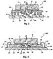
- FIGS. 3 and 3 Aillustrate a third embodiment of the present invention designated as a wire bond style/flip-chip attachment assembly 300 .
- the assembly 300comprises an inverted semiconductor die 12 having active surface 14 with at least one bond pad 38 on the semiconductor die active surface 14 .
- the bond pads 38are arranged in two rows extending down the longitudinal axis of semiconductor die 12 being located transverse to the plane of the page, such an arrangement commonly being used for a “leads over” connection to frame leads extending over the die in its normal, upright position.
- the semiconductor die active surface 14is bonded to the adaptor board upper surface 20 with an insulating, sealing adhesive 40 .
- the adaptor board 18includes at least one or more wire bond vias 42 which is located in a position or positions aligned with the semiconductor die bond pads 38 .
- Each individual wire bond 134is connected to each corresponding individual semiconductor die bond pad 38 .
- Each wire bond 134extends from the semiconductor die bond pad 38 to a corresponding bond pad or lead 39 on the adaptor board lower surface 24 , which communicates with master board connectors 22 through circuit traces 23 .
- the master board terminals 31are in electrical communication with at least one master board connector 22 extending substantially perpendicularly from the adaptor board lower surface 24 .
- a sealant 44encases the bond wires 134 and seals the wire bond via 42 to prevent contamination and damage to the wire bonds.
- FIG. 4illustrates a fourth embodiment of the present invention designated as a wire bond style/wire bond attachment assembly 400 .
- the assembly 400comprises the semiconductor die 12 having active surface 14 with at least one bond pad 38 on the semiconductor die active surface 14 .
- semiconductor die 12in this instance employs bond pads 38 in a “leads over” configuration.
- the semiconductor die active surface 14is bonded to the adaptor board upper surface 20 with an insulating, sealing adhesive 40 .
- the adaptor board 18includes at least one wire bond via 42 which is located in a position or positions aligned with the semiconductor die bond pads 38 .
- Each individual wire bond 134is connected to each corresponding semiconductor die bond pad 38 .
- Each wire bond 134extends from the semiconductor die bond pad 38 to a corresponding bond pad 46 within the wire bond via 42 .
- the via bond pads 46are in electrical communication through circuit traces 23 with at least one corresponding adaptor board bond pad 28 .
- the adaptor board lower surface 24is bonded to the master board upper surface 36 with the adhesive 32 .
- Wire bonds 34extend from the adapter board upper surface 20 to a corresponding bond pad or lead on the master board upper surface 36 .
- the wire bond via sealant 44encases the bond wires 134 and seals the wire bond via 42 to prevent contamination.
Landscapes
- Engineering & Computer Science (AREA)
- Microelectronics & Electronic Packaging (AREA)
- Computer Hardware Design (AREA)
- Power Engineering (AREA)
- Physics & Mathematics (AREA)
- Condensed Matter Physics & Semiconductors (AREA)
- General Physics & Mathematics (AREA)
- Manufacturing & Machinery (AREA)
- Ceramic Engineering (AREA)
- Wire Bonding (AREA)
- Electric Connection Of Electric Components To Printed Circuits (AREA)
Abstract
Description
- This application is a continuation of application Ser. No. 09/699,537, filed Oct. 30, 2000, now U.S. Pat. No. 6,861,290, issued Mar. 1, 2005, which is a divisional of application Ser. No. 09/483,483, filed Jan. 14, 2000, now U.S. Pat. No. 6,265,766, issued Jul. 24, 2001, which is a continuation of application Ser. No. 08/948,936, filed Oct. 10, 1997, now U.S. Pat. No. 6,201,304, issued Mar. 13, 2001, which is a continuation of application Ser. No. 08/574,662, filed Dec. 19, 1995, now U.S. Pat. No. 5,719,440, issued Feb. 17, 1998.
- 1. Field of the Invention
- The present invention relates to an apparatus for connecting a bare semiconductor die having a size and bond pad arrangement, either solder ball arrangement, or pin arrangement (hereinafter referred to generally as a “terminal arrangement”), which does not conform to a printed circuit board with a specific or standardized pin out, connector pad, or lead placement (hereinafter referred to generally as a “connection arrangement”). More particularly, the present invention relates to an intermediate conductor-carrying substrate (hereinafter referred to generally as an “adaptor board”) for connecting a non-conforming bare die to another printed circuit board having a given connection arrangement (hereinafter referred to generally as a “master board”).
- 2. State of the Art
- Definitions: The following terms and acronyms will be used throughout the application and are defined as follows:
- BGA—Ball Grid Array: An array of minute solder balls disposed on an attachment surface of a semiconductor die wherein the solder balls are refluxed for simultaneous attachment and electrical communication of the semiconductor die to a printed circuit board.
- COB—Chip On Board: The techniques used to attach semiconductor dice to a printed circuit board, including flip-chip attachment, wire bonding, and tape automated bonding (“TAB”).
- Flip-Chip: A chip or die that has bumped terminations spaced around the active surface of the die and is intended for facedown mounting.
- Flip-Chip Attachment: A method of attaching a semiconductor die to a substrate in which the die is flipped so that the connecting conductor pads on the face of the die are set on mirror-image pads on the substrate (i.e. printed circuit board) and bonded by refluxing the solder.
- Glob Top: A glob of encapsulant material (usually epoxy or silicone or a combination thereof) surrounding a semiconductor die in the COB assembly process.
- PGA—Pin Grid Array: An array of small pins extending substantially perpendicularly from the major plane of a semiconductor die, wherein the pins conform to a specific arrangement on a printed circuit board for attachment thereto.
- SLICC—Slightly Larger than Integrated Circuit Carrier: An array of minute solder balls disposed on an attachment surface of a semiconductor die similar to a BGA, but having a smaller solder ball pitch and diameter than a BGA.
- State-of-the-art COB technology generally consists of three semiconductor dies to printed circuit boards attachment techniques: flip-chip attachment, wire bonding, and TAB.
- Flip-chip attachment consists of attaching a semiconductor die, generally having a BGA, a SLICC or a PGA, to a printed circuit board. With the BGA or SLICC, the solder ball arrangement on the semiconductor die must be a mirror-image of the connecting bond pads on the printed circuit board such that precise connection is made. The semiconductor die is bonded to the printed circuit board by refluxing the solder balls. With the PGA, the pin arrangement of the semiconductor die must be a mirror-image of the pin recesses on the printed circuit board. After insertion, the semiconductor die is generally bonded by soldering the pins into place. An under-fill encapsulant is generally disposed between the semiconductor die and the printed circuit board to prevent contamination. A variation of the pin-in-recess PGA is a J-lead PGA, wherein the loops of the Js are soldered to pads on the surface of the circuit board. Nonetheless, the lead and pad locations must coincide, as with the other referenced flip-chip techniques.
- Wire bonding and TAB attachment generally begins with attaching a semiconductor die to the surface of a printed circuit board with an appropriate adhesive. In wire bonding, a plurality of bond wires are attached, one at a time, from each bond pad on the semiconductor die and to a corresponding lead on the printed circuit board. The bond wires are generally attached through one of three industry-standard wire bonding techniques: ultrasonic bonding, using a combination of pressure and ultrasonic vibration bursts to form a metallurgical cold weld; thermocompression bonding, using a combination of pressure and elevated temperature to form a weld; and thermosonic bonding, using a combination of pressure, elevated temperature, and ultrasonic vibration bursts. The die may be oriented either face up or face down (with its active surface and bond pads either up or down with respect to the circuit board) for wire bonding, although face up orientation is more common. With TAB, metal tape leads are attached between the bond pads on the semiconductor die and the leads on the printed circuit board. An encapsulant is generally used to cover the bond wires and metal tape leads to prevent contamination.
- Although the foregoing methods are effective for bonding semiconductor dice to printed circuit boards, the terminal arrangements of the dice and the connection arrangements of the boards must be designed to accommodate one another. Thus, it may be impossible to electrically connect a particular semiconductor die to a printed circuit board for which the semiconductor die terminal arrangement was not designed to match the board's connection arrangement. With either wire bond or TAB attachment, the semiconductor die bond pad may not correspond to the lead ends on the circuit board, and thus attachment is either impossible or extremely difficult due to the need for overlong wires and the potential for inter-wire contact and shorting. With flip-chip attachment, if the printed circuit board connection arrangement is not a mirror-image of the solder ball or pin arrangement (terminal arrangement) on the semiconductor die, electrically connecting the flip-chip to the printed circuit board is impossible.
- Therefore, it would be advantageous to develop an apparatus for connecting a semiconductor die having a size and bond pad arrangement, solder ball arrangement, or pin arrangement (“I/O pattern”) which does not conform to a printed circuit board with a specific or standardized pin out, connection pad location, or lead placement (“I/O pattern”).
- The present invention relates to an intermediate printed circuit board or other conductor-carrying substrate that functions as an adaptor board for electrically connecting one or more bare semiconductor dice of a variety of sizes and bond pad locations, solder ball arrangement, or pin arrangement, to a master printed circuit board with a specific or standardized pin out, connector pad location, or lead placement.
- An adaptor printed circuit board or substrate (“adaptor board”) is sized and configured with an I/O pattern to accommodate its attachment to the master printed circuit board (“master board”). If the master board is configured to receive a specific pin out or specific connector pad locations, the adaptor board is configured on its master board attachment surface with pins or solder balls in mirror-image to the master board connection arrangement to make electrical contact with the specific pin out or connector pads on the printed circuit board. If the master board is configured to receive a bond wire, the adaptor board is configured and sized to provide wire bond pads on its upper surface closely adjacent the bond pads of the master board leads. The adaptor board can, of course, be configured to accommodate other attachment and electrical connection means known in the industry, as well as other components in addition to the semiconductor die or dice carried thereon.
- On the semiconductor die side of the adaptor board, one or more semiconductor dice are attached. If a “flip-chip” die is attached to the adaptor board, the adaptor board will, of course, be configured with an I/O pattern to receive the flip-chip with a specific pin out or connector pad locations. The pin out or connector pads on the adaptor board are connected to circuit traces on or through the adaptor board. The circuit traces form the electrical communication path from the pin recesses or connector pads on the adaptor board to the connection points to the master board.
- If a “leads over” die is used with the adaptor board, the bond pads on the die are wire bonded to the adaptor board. Preferably, the leads over die is attached to the adaptor board with the bond pads facing the adaptor board. The bond wires are attached to the leads over die bond pads and extend into a via or vias in the adaptor board. The bond wires are attached to an I/O pattern of adaptor board bond pads within the via from which circuit traces extend, or to leads on the master board side of the adaptor board.
- It is, of course, understood that the leads over die can be attached to the adaptor board with the bond pads facing away from the adaptor board. Thus, the bond wires are simply attached to the bond pads on the leads over die and to a corresponding I/O pattern of adaptor board pad on the semiconductor die side of the adaptor board.
- Preferably, the exposed circuitry of the die and the die-to-adaptor board interconnection is sealed from contamination by a glob top after wire bonding or an underflow compound in the case of a flip-chip attachment.
- Furthermore, it is understood that with the use of wire bonds, the adaptor boards can be stacked on top of each other and connected to the adaptor board as by wire bonding.
- While the specification concludes with claims particularly pointing out and distinctly claiming that which is regarded as the present invention, the advantages of this invention can be more readily ascertained from the following description of the invention when read in conjunction with the accompanying drawings in which:
FIG. 1 is a side view of one embodiment of the present invention;FIG. 2 is a side view of a second embodiment of the present invention;FIG. 2A is a top view of the second embodiment of the present invention shown inFIG. 2 ;FIG. 3 is a side view of a third embodiment of the present invention;FIG. 3A is an upside-down exploded perspective view of selected portions of the third embodiment; andFIG. 4 is a side view of a fourth embodiment of the present invention.FIG. 1 illustrates a first embodiment of the present invention designated as a flip-chip style/flip-chip attachment assembly 100.Assembly 100 comprises asemiconductor die 12 having an invertedactive surface 14 with at least one flip-chip electric connection16 (such as a C4 solder bump connection, a pin connection, or a surface mount j-lead connection, by way of example) extending substantially perpendicularly from abond pad 15 on the semiconductor dieactive surface 14. The flip-chipelectric connections 16 are attached to anupper surface 20 of anadaptor board 18 in such a manner that the flip-chipelectric connections 16 make electrical contact withelectrical contact elements 21 in or on the surface ofadaptor board 18. Theelectrical contact elements 21 make electrical communication between each flip-chipelectric connection 16, through circuit traces23 (exemplary traces shown in broken lines) in theadaptor board 18, to at least onemaster board connector 22 extending substantially perpendicularly from alower surface 24 of theadaptor board 18 to connectadaptor board 18 to an alignedterminal 31 onmaster board 30. Preferably, a sealingcompound 26 is disposed between the semiconductor die12 and theadaptor board 18 to prevent contamination of the flip-chipelectric connections 16 and to more firmly secure semiconductor die12 toadaptor board 18.- In actual practice, there will be a plurality of
terminals 31 arranged in a specific, perhaps industry-standard pattern, onmaster board 30, and master board connectors will be arranged in a mirror-image pattern toterminals 31 for mating connection therewith.Master board connectors 22 andterminals 31 may comprise any electrical connection mechanism known in the art, in addition to those previously described herein. FIGS. 2 and 2 A illustrate a second embodiment of the present invention designated as a flip-chip style/wirebond attachment assembly 200. Components common to bothFIG. 1 andFIG. 2 retain the same numeric designation. Theassembly 200 comprises the semiconductor die12 havingactive surface 14 with at least one flip-chipelectric connection 16, as known in the art, extending substantially perpendicularly from abond pad 15 on the semiconductor dieactive surface 14. The flip-chipelectric connections 16 are attached to the adaptor boardupper surface 20 in such a manner that the flip-chipelectric connections 16 make electrical contact withelectrical contact elements 21 on theadaptor board 18. Theelectrical contact elements 21 communicate between each flip-chipelectric connection 16 tobond pads 28 on the adaptor boardupper surface 20 through circuit traces23. The adaptor boardlower surface 24 is bonded to anupper surface 36 of amaster board 30 with an adhesive32, which may comprise a liquid or gel adhesive, or an adhesive tape, all as known in the art. If desired, adhesive32 may be a heat-conductive adhesive. Awire bond 34 extends from each adaptorboard bond pad 28 to a corresponding bond pad orlead end 35 on theupper surface 36 ofmaster board 30, bond pad orlead end 35 communicating with other components mounted tomaster board 30 or with other components on other boards or other assemblies through circuit traces or other conductors known in the art.FIGS. 3 and 3 A illustrate a third embodiment of the present invention designated as a wire bond style/flip-chip attachment assembly 300. Components which are common to the previous figures retain the same numeric designation. Theassembly 300 comprises an inverted semiconductor die12 havingactive surface 14 with at least onebond pad 38 on the semiconductor dieactive surface 14. As illustrated, thebond pads 38 are arranged in two rows extending down the longitudinal axis of semiconductor die12 being located transverse to the plane of the page, such an arrangement commonly being used for a “leads over” connection to frame leads extending over the die in its normal, upright position. The semiconductor dieactive surface 14 is bonded to the adaptor boardupper surface 20 with an insulating, sealingadhesive 40. Theadaptor board 18 includes at least one or morewire bond vias 42 which is located in a position or positions aligned with the semiconductor diebond pads 38. Eachindividual wire bond 134 is connected to each corresponding individual semiconductor diebond pad 38. Eachwire bond 134 extends from the semiconductor diebond pad 38 to a corresponding bond pad or lead39 on the adaptor boardlower surface 24, which communicates withmaster board connectors 22 through circuit traces23. Themaster board terminals 31 are in electrical communication with at least onemaster board connector 22 extending substantially perpendicularly from the adaptor boardlower surface 24. Preferably, asealant 44 encases thebond wires 134 and seals the wire bond via42 to prevent contamination and damage to the wire bonds.FIG. 4 illustrates a fourth embodiment of the present invention designated as a wire bond style/wirebond attachment assembly 400. Components which are common to the previous figures retain the same numeric designation. Theassembly 400 comprises the semiconductor die12 havingactive surface 14 with at least onebond pad 38 on the semiconductor dieactive surface 14. As with the embodiment ofFIG. 3 , semiconductor die12 in this instance employsbond pads 38 in a “leads over” configuration. The semiconductor dieactive surface 14 is bonded to the adaptor boardupper surface 20 with an insulating, sealingadhesive 40. Theadaptor board 18 includes at least one wire bond via42 which is located in a position or positions aligned with the semiconductor diebond pads 38. Eachindividual wire bond 134 is connected to each corresponding semiconductor diebond pad 38. Eachwire bond 134 extends from the semiconductor diebond pad 38 to acorresponding bond pad 46 within the wire bond via42. The viabond pads 46 are in electrical communication through circuit traces23 with at least one corresponding adaptorboard bond pad 28. The adaptor boardlower surface 24 is bonded to the master boardupper surface 36 with the adhesive32.Wire bonds 34 extend from the adapter boardupper surface 20 to a corresponding bond pad or lead on the master boardupper surface 36. Preferably, the wire bond viasealant 44 encases thebond wires 134 and seals the wire bond via42 to prevent contamination.- Having thus described in detail preferred embodiments of the present invention, it is to be understood that the invention defined by the appended claims is not to be limited by particular details set forth in the above description as many apparent variations thereof are possible without departing from the spirit or scope thereof.
Claims (10)
1. A method of forming a wire bond style/flip chip attach assembly using an inverted bare semiconductor die having a surface having a plurality of bond pads extending along a longitudinal axis of said semiconductor die on said surface in a first bond pad pattern different than the connector pattern arrangement of the first substrate and using a second adapter substrate having a die side surface, a second attachment surface, at least one via extending through the substrate from the die side surface to the second attachment surface, a plurality of circuits, and a plurality of bond pads located on the second attachment surface having a connector pattern connected to the plurality of circuits matching the connector pattern arrangement of the first substrate and a plurality of bond pads located in a first bond pad pattern connected to the plurality of circuits matching the first bond pad pattern of the bare semiconductor die comprising:
applying an adhesive to a portion of the die side of the first substrate to attach the inverted bare semiconductor die thereto for attaching a portion of the surface having a plurality of bond pads thereon of the inverted bare semiconductor die to a portion of the die side surface of said second substrate locating the bare semiconductor die above the second adapter substrate having the bond pads of the semiconductor die located over the via in the second adapter substrate;
connecting said plurality of bond pads of the inverted bare semiconductor die to said plurality of bond pads on the second attachment surface of said second adapter substrate using a plurality of wire bonds, said plurality of wire bonds extending through said at least one via extending from bond pads of the semiconductor die located on the die side surface of the second adapter substrate through said second adapter substrate to the second attachment surface of the second adapter substrate, the plurality of wire bonds connected to the first bond pad pattern of the inverted semiconductor die and to the matching first bond pad pattern on the second attachment surface of the second adapter substrate;
filling at least a portion of the via in the substrate with a sealant; and
connecting said second adapter substrate to said first substrate having said second substrate located solely on one side of said first substrate, the connections between said first substrate and said adapter second substrate formed by a plurality of adapter board connectors extending between the matching connector pattern on the second attachment surface of the second adapter substrate to the connector arrangement of the first substrate.
2. A method of forming a wire bond style/flip chip attach assembly electrically connecting a semiconductor die having a first bond pad pattern to a master board having a connector pattern arrangement using an inverted bare semiconductor die having a plurality of bond pads located in at least two rows extending down the longitudinal axis of inverted the bare semiconductor die thereon, the at least two rows of bond pads having a first bond pad pattern, a a master board having a plurality of circuit traces on an upper surface thereof connected to a plurality of connectors in a second connector pattern arrangement located thereon different than the first bond pad pattern of the plurality of bond pads of the inverted bare semiconductor die, an adapter board having a die side surface, a second attachment surface, a via extending through the adapter board from the die side surface to the second attachment surface, a plurality of circuits, a plurality of bond pads located on the second attachment surface of the adapter board having a plurality of bond pads connected to the plurality of circuits matching the first bond pad pattern of the plurality of bond pads of the inverted bare semiconductor die, and having a connector pattern connected to the plurality of circuits matching the connector pattern arrangement of the plurality of connectors of the master board, and a plurality of electrical connectors for connecting the connector pattern connected to the plurality of circuits matching the connector pattern arrangement of the plurality of connectors of the master board located on the second attachment surface of the adapter board to the plurality of connectors in a second connector pattern arrangement of the circuit traces of the master board, the method comprising:
attaching a portion of said inverted bare semiconductor die to a portion of the die side surface of the adapter board;
connecting said plurality of bond pads of said inverted bare semiconductor die to said plurality of bond pads of the adapter board using a plurality of wire bonds, said plurality of wire bonds extending through the via extending through the adapter board having a portion thereof attached to the plurality of bond pads on the second attachment surface of the adapter board and having a portion thereof attached to the plurality of bond pads on the bare semiconductor die; and
connecting said adapter board and master board using said plurality of electrical connectors on said adapter board to said plurality of circuit traces on said master board using the plurality of electrical connectors.
3. A method of forming a wire bond style/flip chip attach assembly attaching a semiconductor die having a first bond pad pattern to a first substrate having a connector pattern arrangement for attaching said first substrate to a second adapter substrate having an upper surface and having a second surface having a connector pattern thereon and having a plurality of circuit traces thereon using an inverted bare semiconductor die having a surface having a plurality of bond pads located along a longitudinal axis of said die on said surface extending in a leads-over configuration on said surface, the plurality of bond pads having a first bond pad pattern different than the connector pattern arrangement of the first substrate and a second adapter substrate having a die side surface, a second attachment surface, at least one via extending through the board from the die side surface to the second attachment surface, a plurality of circuits, and a plurality of bond pads located on the second attachment surface of the second adapter substrate having a connector pattern thereon connected to the plurality of circuits matching the connector pattern arrangement of the first substrate and a plurality of bond pads connected to the plurality of circuits in a bond pad pattern matching the first bond pad pattern of the inverted bare semiconductor die, the method comprising:
applying an adhesive to a portion of the die side of the second adapter substrate to attach the inverted bare semiconductor die thereto;
attaching a portion of the surface having a plurality of bond pads thereon of the bare semiconductor die to a portion of the die side surface of said second substrate;
connecting said plurality of bond pads of the inverted bare semiconductor die to said plurality of bond pads of said second adapter substrate using a plurality of bond wires, said plurality of bond wires extending through said at least one via extending through said second adapter substrate, the plurality of bond wires connected to the first bond pad pattern of the plurality of bond pads of the inverted semiconductor die and to the matching first bond pad pattern of the plurality of bond pads on the second attachment surface of the second adapter substrate; and
attaching said first substrate to said second attachment surface of said second adapter substrate using a plurality of adapter board connectors extending from the second attachment surface of the second adapter substrate.
4. A method of forming a wire bond style/flip chip attach assembly attaching a semiconductor die to a master board using an inverted bare semiconductor die having a plurality of bond pads in at least two rows having a first bond pad arrangement located down the longitudinal axis of a surface of the inverted bare semiconductor die in a leads over chip configuration, a master board having a plurality of circuit traces on an upper surface thereof connected to a plurality of connectors in a connector pattern arrangement located thereon, said upper surface for the receipt of an adapter board therein, an adapter board having a die side surface, a second attachment surface, at least one via extending through the adapter board from the die side surface to the second attachment surface, a plurality of circuits, a plurality of bond pads located on the second attachment surface of the adapter board having a plurality of bond pads connected to the plurality of circuits in a first bond pad pattern matching the first bond pad pattern of the inverted bare semiconductor die, and having a connector pattern thereon connected to the plurality of circuits matching the connector pattern arrangement of the master board, and a plurality of electrical connectors for connecting the connector pattern of the plurality of circuits located on the second attachment surface of the adapter board to the plurality of circuits of the master board, the method comprising:
attaching a portion of said inverted bare semiconductor die to a portion of the die side surface of the adapter board;
connecting said plurality of bond pads in a first bond pad arrangement of said bare semiconductor die to said plurality of bond pads in a matching first bond pad pattern of said adapter board using a plurality of bond wires extending through the via extending through the adapter board from the die side surface to the second attachment surface; and
connecting said adapter board and master board using said plurality of electrical connectors on said board to said at least one circuit trace on said master board using adapter board.
5. An assembly for a semiconductor die to a master board comprising:
a master board;
a bare semiconductor die having non-conforming arrangements for a standardized pin out, for standardized connector pad locations, or for standardized lead placement on said master board; and
a board having a die side surface and an attachment surface wherein said master board is electrically connected to said board attachment surface, and said bare semiconductor die is electrically connected to said board die side surface; said board having circuit traces for electrical communication between said bare semiconductor die and said master board.
6. The assembly ofclaim 5 , wherein the electrical connection between said board and said master board attachment side surface comprises refluxed solder balls protruding from the attachment surface of the board.
7. The assembly ofclaim 5 , wherein the electrical connection between said semiconductor die and board die side surface comprises pins extending between an attachment surface of said semiconductor die which are attached to said board die side surface.
8. The assembly ofclaim 5 , wherein the electrical connection between said semiconductor die and said board comprises bond wires.
9. The assembly ofclaim 8 , wherein the board includes at least one via extending therethrough.
10. The assembly ofclaim 9 , wherein said bond wires are electrically connected with said semiconductor die and extend through said via to electrically connect to said attachment side of the board.
Priority Applications (6)
| Application Number | Priority Date | Filing Date | Title |
|---|---|---|---|
| US11/070,364US7329945B2 (en) | 1995-12-19 | 2005-03-01 | Flip-chip adaptor package for bare die |
| US11/437,550US7381591B2 (en) | 1995-12-19 | 2006-05-19 | Flip-chip adaptor package for bare die |
| US11/866,065US8198138B2 (en) | 1995-12-19 | 2007-10-02 | Methods for providing and using grid array packages |
| US12/714,130US8049317B2 (en) | 1995-12-19 | 2010-02-26 | Grid array packages |
| US12/714,193US8164175B2 (en) | 1995-12-19 | 2010-02-26 | Stackable semiconductor device assemblies |
| US12/714,163US8299598B2 (en) | 1995-12-19 | 2010-02-26 | Grid array packages and assemblies including the same |
Applications Claiming Priority (5)
| Application Number | Priority Date | Filing Date | Title |
|---|---|---|---|
| US08/574,662US5719440A (en) | 1995-12-19 | 1995-12-19 | Flip chip adaptor package for bare die |
| US08/948,936US6201304B1 (en) | 1995-12-19 | 1997-10-10 | Flip chip adaptor package for bare die |
| US09/483,483US6265766B1 (en) | 1995-12-19 | 2000-01-14 | Flip chip adaptor package for bare die |
| US09/699,537US6861290B1 (en) | 1995-12-19 | 2000-10-30 | Flip-chip adaptor package for bare die |
| US11/070,364US7329945B2 (en) | 1995-12-19 | 2005-03-01 | Flip-chip adaptor package for bare die |
Related Parent Applications (1)
| Application Number | Title | Priority Date | Filing Date |
|---|---|---|---|
| US09/699,537ContinuationUS6861290B1 (en) | 1995-12-19 | 2000-10-30 | Flip-chip adaptor package for bare die |
Related Child Applications (1)
| Application Number | Title | Priority Date | Filing Date |
|---|---|---|---|
| US11/437,550ContinuationUS7381591B2 (en) | 1995-12-19 | 2006-05-19 | Flip-chip adaptor package for bare die |
Publications (2)
| Publication Number | Publication Date |
|---|---|
| US20050167850A1true US20050167850A1 (en) | 2005-08-04 |
| US7329945B2 US7329945B2 (en) | 2008-02-12 |
Family
ID=27413651
Family Applications (7)
| Application Number | Title | Priority Date | Filing Date |
|---|---|---|---|
| US09/699,537Expired - Fee RelatedUS6861290B1 (en) | 1995-12-19 | 2000-10-30 | Flip-chip adaptor package for bare die |
| US11/070,364Expired - Fee RelatedUS7329945B2 (en) | 1995-12-19 | 2005-03-01 | Flip-chip adaptor package for bare die |
| US11/437,550Expired - Fee RelatedUS7381591B2 (en) | 1995-12-19 | 2006-05-19 | Flip-chip adaptor package for bare die |
| US11/866,065Expired - Fee RelatedUS8198138B2 (en) | 1995-12-19 | 2007-10-02 | Methods for providing and using grid array packages |
| US12/714,163Expired - Fee RelatedUS8299598B2 (en) | 1995-12-19 | 2010-02-26 | Grid array packages and assemblies including the same |
| US12/714,193Expired - Fee RelatedUS8164175B2 (en) | 1995-12-19 | 2010-02-26 | Stackable semiconductor device assemblies |
| US12/714,130Expired - Fee RelatedUS8049317B2 (en) | 1995-12-19 | 2010-02-26 | Grid array packages |
Family Applications Before (1)
| Application Number | Title | Priority Date | Filing Date |
|---|---|---|---|
| US09/699,537Expired - Fee RelatedUS6861290B1 (en) | 1995-12-19 | 2000-10-30 | Flip-chip adaptor package for bare die |
Family Applications After (5)
| Application Number | Title | Priority Date | Filing Date |
|---|---|---|---|
| US11/437,550Expired - Fee RelatedUS7381591B2 (en) | 1995-12-19 | 2006-05-19 | Flip-chip adaptor package for bare die |
| US11/866,065Expired - Fee RelatedUS8198138B2 (en) | 1995-12-19 | 2007-10-02 | Methods for providing and using grid array packages |
| US12/714,163Expired - Fee RelatedUS8299598B2 (en) | 1995-12-19 | 2010-02-26 | Grid array packages and assemblies including the same |
| US12/714,193Expired - Fee RelatedUS8164175B2 (en) | 1995-12-19 | 2010-02-26 | Stackable semiconductor device assemblies |
| US12/714,130Expired - Fee RelatedUS8049317B2 (en) | 1995-12-19 | 2010-02-26 | Grid array packages |
Country Status (1)
| Country | Link |
|---|---|
| US (7) | US6861290B1 (en) |
Cited By (5)
| Publication number | Priority date | Publication date | Assignee | Title |
|---|---|---|---|---|
| US20070013040A1 (en)* | 2002-06-19 | 2007-01-18 | United Test & Assembly Center Limited | Packaging of a microchip device |
| SG130061A1 (en)* | 2005-08-24 | 2007-03-20 | Micron Technology Inc | Microelectronic devices and microelectronic support devices, and associated assemblies and methods |
| US20090236755A1 (en)* | 2008-03-19 | 2009-09-24 | Cheng-Ting Wu | Chip package structure |
| US20190281698A1 (en)* | 2018-03-12 | 2019-09-12 | Dell Products, Lp | System and Method for Minimizing Connector Pad Open-Circuit Stubs |
| US20240079369A1 (en)* | 2022-09-06 | 2024-03-07 | Micron Technology, Inc. | Connecting semiconductor dies through traces |
Families Citing this family (75)
| Publication number | Priority date | Publication date | Assignee | Title |
|---|---|---|---|---|
| JP3487524B2 (en)* | 1994-12-20 | 2004-01-19 | 株式会社ルネサステクノロジ | Semiconductor device and manufacturing method thereof |
| US6861290B1 (en) | 1995-12-19 | 2005-03-01 | Micron Technology, Inc. | Flip-chip adaptor package for bare die |
| USRE43112E1 (en) | 1998-05-04 | 2012-01-17 | Round Rock Research, Llc | Stackable ball grid array package |
| AU2005322072A1 (en) | 2004-12-27 | 2006-07-06 | Quantum Paper, Inc. | Addressable and printable emissive display |
| KR100810349B1 (en)* | 2006-08-04 | 2008-03-04 | 삼성전자주식회사 | Interposers and Semiconductor Packages Using the Same |
| US8619378B2 (en) | 2010-11-15 | 2013-12-31 | DigitalOptics Corporation MEMS | Rotational comb drive Z-stage |
| US8768157B2 (en) | 2011-09-28 | 2014-07-01 | DigitalOptics Corporation MEMS | Multiple degree of freedom actuator |
| DE102008001226A1 (en)* | 2007-04-24 | 2008-10-30 | Ceramtec Ag | Component with a metallized ceramic body |
| US8384630B2 (en) | 2007-05-31 | 2013-02-26 | Nthdegree Technologies Worldwide Inc | Light emitting, photovoltaic or other electronic apparatus and system |
| US8415879B2 (en) | 2007-05-31 | 2013-04-09 | Nthdegree Technologies Worldwide Inc | Diode for a printable composition |
| US8889216B2 (en) | 2007-05-31 | 2014-11-18 | Nthdegree Technologies Worldwide Inc | Method of manufacturing addressable and static electronic displays |
| US8133768B2 (en) | 2007-05-31 | 2012-03-13 | Nthdegree Technologies Worldwide Inc | Method of manufacturing a light emitting, photovoltaic or other electronic apparatus and system |
| US9419179B2 (en) | 2007-05-31 | 2016-08-16 | Nthdegree Technologies Worldwide Inc | Diode for a printable composition |
| US8674593B2 (en) | 2007-05-31 | 2014-03-18 | Nthdegree Technologies Worldwide Inc | Diode for a printable composition |
| US8809126B2 (en) | 2007-05-31 | 2014-08-19 | Nthdegree Technologies Worldwide Inc | Printable composition of a liquid or gel suspension of diodes |
| US9534772B2 (en) | 2007-05-31 | 2017-01-03 | Nthdegree Technologies Worldwide Inc | Apparatus with light emitting diodes |
| US9425357B2 (en) | 2007-05-31 | 2016-08-23 | Nthdegree Technologies Worldwide Inc. | Diode for a printable composition |
| US9018833B2 (en) | 2007-05-31 | 2015-04-28 | Nthdegree Technologies Worldwide Inc | Apparatus with light emitting or absorbing diodes |
| US8846457B2 (en) | 2007-05-31 | 2014-09-30 | Nthdegree Technologies Worldwide Inc | Printable composition of a liquid or gel suspension of diodes |
| US9343593B2 (en) | 2007-05-31 | 2016-05-17 | Nthdegree Technologies Worldwide Inc | Printable composition of a liquid or gel suspension of diodes |
| US8877101B2 (en) | 2007-05-31 | 2014-11-04 | Nthdegree Technologies Worldwide Inc | Method of manufacturing a light emitting, power generating or other electronic apparatus |
| US8852467B2 (en) | 2007-05-31 | 2014-10-07 | Nthdegree Technologies Worldwide Inc | Method of manufacturing a printable composition of a liquid or gel suspension of diodes |
| WO2009035849A2 (en) | 2007-09-10 | 2009-03-19 | Vertical Circuits, Inc. | Semiconductor die mount by conformal die coating |
| CN101999167B (en)* | 2008-03-12 | 2013-07-17 | 伊文萨思公司 | Support mounted electrically interconnected die assembly |
| US7992332B2 (en) | 2008-05-13 | 2011-08-09 | Nthdegree Technologies Worldwide Inc. | Apparatuses for providing power for illumination of a display object |
| US8127477B2 (en) | 2008-05-13 | 2012-03-06 | Nthdegree Technologies Worldwide Inc | Illuminating display systems |
| US9153517B2 (en) | 2008-05-20 | 2015-10-06 | Invensas Corporation | Electrical connector between die pad and z-interconnect for stacked die assemblies |
| FR2932004B1 (en)* | 2008-06-03 | 2011-08-05 | Commissariat Energie Atomique | STACKED ELECTRONIC DEVICE AND METHOD FOR PRODUCING SUCH AN ELECTRONIC DEVICE |
| US9157167B1 (en) | 2008-06-05 | 2015-10-13 | Soraa, Inc. | High pressure apparatus and method for nitride crystal growth |
| US9543392B1 (en) | 2008-12-12 | 2017-01-10 | Soraa, Inc. | Transparent group III metal nitride and method of manufacture |
| US8084853B2 (en)* | 2009-09-25 | 2011-12-27 | Mediatek Inc. | Semiconductor flip chip package utilizing wire bonding for net switching |
| US9175418B2 (en) | 2009-10-09 | 2015-11-03 | Soraa, Inc. | Method for synthesis of high quality large area bulk gallium based crystals |
| KR101614856B1 (en)* | 2009-10-12 | 2016-04-22 | 삼성전자주식회사 | Wiring substrate for a semiconductor chip, semiconductor package having the wiring substrate and method of manufacturing the semiconductor package |
| WO2011056668A2 (en) | 2009-10-27 | 2011-05-12 | Vertical Circuits, Inc. | Selective die electrical insulation additive process |
| US9564320B2 (en) | 2010-06-18 | 2017-02-07 | Soraa, Inc. | Large area nitride crystal and method for making it |
| US8803256B2 (en) | 2010-11-15 | 2014-08-12 | DigitalOptics Corporation MEMS | Linearly deployed actuators |
| US9052567B2 (en) | 2010-11-15 | 2015-06-09 | DigitalOptics Corporation MEMS | Actuator inside of motion control |
| US9515579B2 (en) | 2010-11-15 | 2016-12-06 | Digitaloptics Corporation | MEMS electrical contact systems and methods |
| US8521017B2 (en) | 2010-11-15 | 2013-08-27 | DigitalOptics Corporation MEMS | MEMS actuator alignment |
| US8884381B2 (en) | 2010-11-15 | 2014-11-11 | DigitalOptics Corporation MEMS | Guard trench |
| US8605375B2 (en) | 2010-11-15 | 2013-12-10 | DigitalOptics Corporation MEMS | Mounting flexure contacts |
| US8337103B2 (en) | 2010-11-15 | 2012-12-25 | DigitalOptics Corporation MEMS | Long hinge actuator snubbing |
| US8947797B2 (en) | 2010-11-15 | 2015-02-03 | DigitalOptics Corporation MEMS | Miniature MEMS actuator assemblies |
| US8608393B2 (en) | 2010-11-15 | 2013-12-17 | DigitalOptics Corporation MEMS | Capillary actuator deployment |
| US9019390B2 (en) | 2011-09-28 | 2015-04-28 | DigitalOptics Corporation MEMS | Optical image stabilization using tangentially actuated MEMS devices |
| US8637961B2 (en) | 2010-11-15 | 2014-01-28 | DigitalOptics Corporation MEMS | MEMS actuator device |
| US9352962B2 (en) | 2010-11-15 | 2016-05-31 | DigitalOptics Corporation MEMS | MEMS isolation structures |
| US8547627B2 (en) | 2010-11-15 | 2013-10-01 | DigitalOptics Corporation MEMS | Electrical routing |
| US8604663B2 (en) | 2010-11-15 | 2013-12-10 | DigitalOptics Corporation MEMS | Motion controlled actuator |
| US8941192B2 (en) | 2010-11-15 | 2015-01-27 | DigitalOptics Corporation MEMS | MEMS actuator device deployment |
| US9061883B2 (en) | 2010-11-15 | 2015-06-23 | DigitalOptics Corporation MEMS | Actuator motion control features |
| US8616791B2 (en) | 2011-09-28 | 2013-12-31 | DigitalOptics Corporation MEMS | Rotationally deployed actuator devices |
| US8855476B2 (en) | 2011-09-28 | 2014-10-07 | DigitalOptics Corporation MEMS | MEMS-based optical image stabilization |
| US8571405B2 (en)* | 2011-09-28 | 2013-10-29 | DigitalOptics Corporation MEMS | Surface mount actuator |
| US8497579B1 (en)* | 2012-02-16 | 2013-07-30 | Chipbond Technology Corporation | Semiconductor packaging method and structure thereof |
| JP5672283B2 (en)* | 2012-09-20 | 2015-02-18 | 株式会社豊田自動織機 | Wiring board and method for manufacturing wiring board |
| JP6064584B2 (en)* | 2012-12-22 | 2017-01-25 | 日亜化学工業株式会社 | Light emitting device and manufacturing method thereof |
| KR102053349B1 (en) | 2013-05-16 | 2019-12-06 | 삼성전자주식회사 | Semiconductor package |
| US9063172B1 (en)* | 2013-05-16 | 2015-06-23 | M/A-Com Technology Solutions Holdings, Inc. | Step connectors in test fixture for packaged device measurement |
| GB2539137B (en)* | 2014-04-30 | 2019-04-03 | Intel Corp | Integrated circuit assemblies with molding compound |
| KR20160006330A (en)* | 2014-07-08 | 2016-01-19 | 삼성전자주식회사 | Semiconductor Package |
| JPWO2016203967A1 (en)* | 2015-06-15 | 2018-03-29 | ソニー株式会社 | Semiconductor device, electronic device, and manufacturing method |
| DE112015006707B4 (en)* | 2015-07-15 | 2024-03-21 | Yamaha Hatsudoki Kabushiki Kaisha | Method for generating model data |
| US9490195B1 (en) | 2015-07-17 | 2016-11-08 | Invensas Corporation | Wafer-level flipped die stacks with leadframes or metal foil interconnects |
| US9871019B2 (en) | 2015-07-17 | 2018-01-16 | Invensas Corporation | Flipped die stack assemblies with leadframe interconnects |
| US9825002B2 (en) | 2015-07-17 | 2017-11-21 | Invensas Corporation | Flipped die stack |
| US9508691B1 (en) | 2015-12-16 | 2016-11-29 | Invensas Corporation | Flipped die stacks with multiple rows of leadframe interconnects |
| US10566310B2 (en) | 2016-04-11 | 2020-02-18 | Invensas Corporation | Microelectronic packages having stacked die and wire bond interconnects |
| US9595511B1 (en) | 2016-05-12 | 2017-03-14 | Invensas Corporation | Microelectronic packages and assemblies with improved flyby signaling operation |
| US9728524B1 (en) | 2016-06-30 | 2017-08-08 | Invensas Corporation | Enhanced density assembly having microelectronic packages mounted at substantial angle to board |
| US20180114786A1 (en)* | 2016-10-21 | 2018-04-26 | Powertech Technology Inc. | Method of forming package-on-package structure |
| US10580710B2 (en)* | 2017-08-31 | 2020-03-03 | Micron Technology, Inc. | Semiconductor device with a protection mechanism and associated systems, devices, and methods |
| US10381329B1 (en) | 2018-01-24 | 2019-08-13 | Micron Technology, Inc. | Semiconductor device with a layered protection mechanism and associated systems, devices, and methods |
| CN110312363B (en)* | 2019-06-24 | 2020-10-16 | 维沃移动通信有限公司 | Printed circuit board assembly and terminal |
| KR102826858B1 (en)* | 2021-06-01 | 2025-06-30 | 삼성전자주식회사 | Semiconductor package and method for manufacturing semiconductor package |
Citations (94)
| Publication number | Priority date | Publication date | Assignee | Title |
|---|---|---|---|---|
| US3648131A (en)* | 1969-11-07 | 1972-03-07 | Ibm | Hourglass-shaped conductive connection through semiconductor structures |
| US4199777A (en)* | 1976-02-02 | 1980-04-22 | Hitachi, Ltd. | Semiconductor device and a method of manufacturing the same |
| US4371912A (en)* | 1980-10-01 | 1983-02-01 | Motorola, Inc. | Method of mounting interrelated components |
| US4446477A (en)* | 1981-08-21 | 1984-05-01 | Sperry Corporation | Multichip thin film module |
| US4505799A (en)* | 1983-12-08 | 1985-03-19 | General Signal Corporation | ISFET sensor and method of manufacture |
| US4638348A (en)* | 1982-08-10 | 1987-01-20 | Brown David F | Semiconductor chip carrier |
| US4649418A (en)* | 1982-09-27 | 1987-03-10 | U.S. Philips Corporation | Data card and method of manufacturing same |
| US4725924A (en)* | 1985-04-10 | 1988-02-16 | Em Microelectronic-Marin Sa | Electronic unit especially for microcircuit cards and card comprising such a unit |
| US4731645A (en)* | 1982-05-14 | 1988-03-15 | U.S. Philips Corporation | Connection of a semiconductor to elements of a support, especially of a portable card |
| US4829666A (en)* | 1980-05-20 | 1989-05-16 | Gao Gesellschaft Fur Automation Und Organisation Mbh | Method for producing a carrier element for an IC-chip |
| US4841355A (en)* | 1988-02-10 | 1989-06-20 | Amdahl Corporation | Three-dimensional microelectronic package for semiconductor chips |
| US4899107A (en)* | 1988-09-30 | 1990-02-06 | Micron Technology, Inc. | Discrete die burn-in for nonpackaged die |
| US4931853A (en)* | 1986-05-20 | 1990-06-05 | Kabushiki Kaisha Toshiba | IC card and method of manufacturing the same |
| US4992849A (en)* | 1989-02-15 | 1991-02-12 | Micron Technology, Inc. | Directly bonded board multiple integrated circuit module |
| US4992850A (en)* | 1989-02-15 | 1991-02-12 | Micron Technology, Inc. | Directly bonded simm module |
| US4996587A (en)* | 1989-04-10 | 1991-02-26 | International Business Machines Corporation | Integrated semiconductor chip package |
| US5012323A (en)* | 1989-11-20 | 1991-04-30 | Micron Technology, Inc. | Double-die semiconductor package having a back-bonded die and a face-bonded die interconnected on a single leadframe |
| US5022580A (en)* | 1988-03-16 | 1991-06-11 | Plessey Overseas Limited | Vernier structure for flip chip bonded devices |
| US5086018A (en)* | 1991-05-02 | 1992-02-04 | International Business Machines Corporation | Method of making a planarized thin film covered wire bonded semiconductor package |
| US5099309A (en)* | 1990-04-30 | 1992-03-24 | International Business Machines Corporation | Three-dimensional memory card structure with internal direct chip attachment |
| US5107328A (en)* | 1991-02-13 | 1992-04-21 | Micron Technology, Inc. | Packaging means for a semiconductor die having particular shelf structure |
| US5107329A (en)* | 1988-02-26 | 1992-04-21 | Hitachi, Ltd. | Pin-grid array semiconductor device |
| US5128831A (en)* | 1991-10-31 | 1992-07-07 | Micron Technology, Inc. | High-density electronic package comprising stacked sub-modules which are electrically interconnected by solder-filled vias |
| US5188984A (en)* | 1987-04-21 | 1993-02-23 | Sumitomo Electric Industries, Ltd. | Semiconductor device and production method thereof |
| US5191511A (en)* | 1991-02-08 | 1993-03-02 | Kabushiki Kaisha Toshiba | Semiconductor device including a package having a plurality of bumps arranged in a grid form as external terminals |
| US5200363A (en)* | 1990-12-20 | 1993-04-06 | Robert Bosch Gmbh | Method for manufacturing a semiconductor package including a glass support |
| US5216278A (en)* | 1990-12-04 | 1993-06-01 | Motorola, Inc. | Semiconductor device having a pad array carrier package |
| US5218234A (en)* | 1991-12-23 | 1993-06-08 | Motorola, Inc. | Semiconductor device with controlled spread polymeric underfill |
| US5222014A (en)* | 1992-03-02 | 1993-06-22 | Motorola, Inc. | Three-dimensional multi-chip pad array carrier |
| US5231304A (en)* | 1989-07-27 | 1993-07-27 | Grumman Aerospace Corporation | Framed chip hybrid stacked layer assembly |
| US5286679A (en)* | 1993-03-18 | 1994-02-15 | Micron Technology, Inc. | Method for attaching a semiconductor die to a leadframe using a patterned adhesive layer |
| US5291062A (en)* | 1993-03-01 | 1994-03-01 | Motorola, Inc. | Area array semiconductor device having a lid with functional contacts |
| US5293068A (en)* | 1990-02-01 | 1994-03-08 | Hitachi, Ltd. | Semiconductor device |
| US5294750A (en)* | 1990-09-18 | 1994-03-15 | Ngk Insulators, Ltd. | Ceramic packages and ceramic wiring board |
| US5299092A (en)* | 1991-05-23 | 1994-03-29 | Hitachi, Ltd. | Plastic sealed type semiconductor apparatus |
| US5311401A (en)* | 1991-07-09 | 1994-05-10 | Hughes Aircraft Company | Stacked chip assembly and manufacturing method therefor |
| US5313096A (en)* | 1992-03-16 | 1994-05-17 | Dense-Pac Microsystems, Inc. | IC chip package having chip attached to and wire bonded within an overlying substrate |
| US5326428A (en)* | 1993-09-03 | 1994-07-05 | Micron Semiconductor, Inc. | Method for testing semiconductor circuitry for operability and method of forming apparatus for testing semiconductor circuitry for operability |
| US5384689A (en)* | 1993-12-20 | 1995-01-24 | Shen; Ming-Tung | Integrated circuit chip including superimposed upper and lower printed circuit boards |
| US5397921A (en)* | 1993-09-03 | 1995-03-14 | Advanced Semiconductor Assembly Technology | Tab grid array |
| US5397917A (en)* | 1993-04-26 | 1995-03-14 | Motorola, Inc. | Semiconductor package capable of spreading heat |
| US5400003A (en)* | 1992-08-19 | 1995-03-21 | Micron Technology, Inc. | Inherently impedance matched integrated circuit module |
| US5419807A (en)* | 1993-09-03 | 1995-05-30 | Micron Technology, Inc. | Method of providing electrical interconnect between two layers within a silicon substrate, semiconductor apparatus, and method of forming apparatus for testing semiconductor circuitry for operability |
| US5420460A (en)* | 1993-08-05 | 1995-05-30 | Vlsi Technology, Inc. | Thin cavity down ball grid array package based on wirebond technology |
| US5422514A (en)* | 1993-05-11 | 1995-06-06 | Micromodule Systems, Inc. | Packaging and interconnect system for integrated circuits |
| US5426072A (en)* | 1993-01-21 | 1995-06-20 | Hughes Aircraft Company | Process of manufacturing a three dimensional integrated circuit from stacked SOI wafers using a temporary silicon substrate |
| US5434106A (en)* | 1989-12-22 | 1995-07-18 | Texas Instruments Incorporated | Integrated circuit device and method to prevent cracking during surface mount |
| US5434452A (en)* | 1993-11-01 | 1995-07-18 | Motorola, Inc. | Z-axis compliant mechanical IC wiring substrate and method for making the same |
| US5486723A (en)* | 1993-05-27 | 1996-01-23 | Ma Laboratories, Inc. | Packaged integrated circuit add-on card |
| US5489804A (en)* | 1989-08-28 | 1996-02-06 | Lsi Logic Corporation | Flexible preformed planar structures for interposing between a chip and a substrate |
| US5508556A (en)* | 1994-09-02 | 1996-04-16 | Motorola, Inc. | Leaded semiconductor device having accessible power supply pad terminals |
| US5528080A (en)* | 1993-03-05 | 1996-06-18 | Goldstein; Edward F. | Electrically conductive interconnection through a body of semiconductor material |
| US5536685A (en)* | 1994-09-20 | 1996-07-16 | Sun Microsystems, Inc. | Low heat loss and secure chip carrier for cryogenic cooling |
| US5541450A (en)* | 1994-11-02 | 1996-07-30 | Motorola, Inc. | Low-profile ball-grid array semiconductor package |
| US5608265A (en)* | 1993-03-17 | 1997-03-04 | Hitachi, Ltd. | Encapsulated semiconductor device package having holes for electrically conductive material |
| US5615089A (en)* | 1994-07-26 | 1997-03-25 | Fujitsu Limited | BGA semiconductor device including a plurality of semiconductor chips located on upper and lower surfaces of a first substrate |
| US5616958A (en)* | 1995-01-25 | 1997-04-01 | International Business Machines Corporation | Electronic package |
| US5625221A (en)* | 1994-03-03 | 1997-04-29 | Samsung Electronics Co., Ltd. | Semiconductor assembly for a three-dimensional integrated circuit package |
| US5636104A (en)* | 1995-05-31 | 1997-06-03 | Samsung Electronics Co., Ltd. | Printed circuit board having solder ball mounting groove pads and a ball grid array package using such a board |
| US5637536A (en)* | 1993-08-13 | 1997-06-10 | Thomson-Csf | Method for interconnecting semiconductor chips in three dimensions, and component resulting therefrom |
| US5637915A (en)* | 1991-12-27 | 1997-06-10 | Fujitsu Ltd. | Semiconductor device affixed to an upper and a lower leadframe |
| US5639696A (en)* | 1996-01-31 | 1997-06-17 | Lsi Logic Corporation | Microelectronic integrated circuit mounted on circuit board with solder column grid array interconnection, and method of fabricating the solder column grid array |
| US5642261A (en)* | 1993-12-20 | 1997-06-24 | Sgs-Thomson Microelectronics, Inc. | Ball-grid-array integrated circuit package with solder-connected thermal conductor |
| US5648679A (en)* | 1994-09-16 | 1997-07-15 | National Semiconductor Corporation | Tape ball lead integrated circuit package |
| US5714405A (en)* | 1990-06-11 | 1998-02-03 | Hitachi, Ltd. | Semiconductor device |
| US5723907A (en)* | 1996-06-25 | 1998-03-03 | Micron Technology, Inc. | Loc simm |
| US5729432A (en)* | 1995-07-05 | 1998-03-17 | Anam Industrial Col, Ltd. | Ball grid array semiconductor package with improved heat dissipation and dehumidification effect |
| US5734198A (en)* | 1994-11-10 | 1998-03-31 | Micron Technology, Inc. | Multi-layer lead frame for a semiconductor device |
| US5739585A (en)* | 1995-11-27 | 1998-04-14 | Micron Technology, Inc. | Single piece package for semiconductor die |
| US5739588A (en)* | 1994-08-15 | 1998-04-14 | Citizen Watch Co., Ltd. | Semiconductor device |
| US5741622A (en)* | 1995-06-06 | 1998-04-21 | Taiyo Ink Manufacturing Co., Ltd. | One-package photosolder resist composition developable with aqueous alkali solution and method for production of printed circuit board by use thereof |
| US5744862A (en)* | 1996-03-29 | 1998-04-28 | Mitsubishi Denki Kabushiki Kaisha | Reduced thickness semiconductor device with IC packages mounted in openings on substrate |
| US5767575A (en)* | 1995-10-17 | 1998-06-16 | Prolinx Labs Corporation | Ball grid array structure and method for packaging an integrated circuit chip |
| US5770347A (en)* | 1994-11-11 | 1998-06-23 | Taiyo Ink Manufacturing Co., Ltd. | Photocurable and thermosetting coating composition and method for formation of solder mask for printed circuit board |
| US5780923A (en)* | 1997-06-10 | 1998-07-14 | Micron Technology, Inc. | Modified bus bar with Kapton™ tape or insulative material on LOC packaged part |
| US5783866A (en)* | 1996-05-17 | 1998-07-21 | National Semiconductor Corporation | Low cost ball grid array device and method of manufacture thereof |
| US5783870A (en)* | 1995-03-16 | 1998-07-21 | National Semiconductor Corporation | Method for connecting packages of a stacked ball grid array structure |
| US5883426A (en)* | 1996-04-18 | 1999-03-16 | Nec Corporation | Stack module |
| US5893726A (en)* | 1997-12-15 | 1999-04-13 | Micron Technology, Inc. | Semiconductor package with pre-fabricated cover and method of fabrication |
| US5903049A (en)* | 1997-10-29 | 1999-05-11 | Mitsubishi Denki Kabushiki Kaisha | Semiconductor module comprising semiconductor packages |
| US5915169A (en)* | 1995-12-22 | 1999-06-22 | Anam Industrial Co., Ltd. | Semiconductor chip scale package and method of producing such |
| US5915977A (en)* | 1997-06-02 | 1999-06-29 | Micron Technology, Inc. | System and interconnect for making temporary electrical connections with bumped semiconductor components |
| US5920118A (en)* | 1996-12-18 | 1999-07-06 | Hyundai Electronics Industries Co., Ltd. | Chip-size package semiconductor |
| US6013946A (en)* | 1996-09-11 | 2000-01-11 | Samsung Electronics Co., Ltd. | Wire bond packages for semiconductor chips and related methods and assemblies |
| US6013948A (en)* | 1995-11-27 | 2000-01-11 | Micron Technology, Inc. | Stackable chip scale semiconductor package with mating contacts on opposed surfaces |
| US6020629A (en)* | 1998-06-05 | 2000-02-01 | Micron Technology, Inc. | Stacked semiconductor package and method of fabrication |
| US6028365A (en)* | 1998-03-30 | 2000-02-22 | Micron Technology, Inc. | Integrated circuit package and method of fabrication |
| US6046072A (en)* | 1993-03-29 | 2000-04-04 | Hitachi Chemical Company, Ltd. | Process for fabricating a crack resistant resin encapsulated semiconductor chip package |
| US6048755A (en)* | 1998-11-12 | 2000-04-11 | Micron Technology, Inc. | Method for fabricating BGA package using substrate with patterned solder mask open in die attach area |
| US6072233A (en)* | 1998-05-04 | 2000-06-06 | Micron Technology, Inc. | Stackable ball grid array package |
| US6091140A (en)* | 1998-10-23 | 2000-07-18 | Texas Instruments Incorporated | Thin chip-size integrated circuit package |
| US6201304B1 (en)* | 1995-12-19 | 2001-03-13 | Micron Technology, Inc. | Flip chip adaptor package for bare die |
| US6372527B1 (en)* | 1990-09-24 | 2002-04-16 | Tessera, Inc. | Methods of making semiconductor chip assemblies |
| US20050087855A1 (en)* | 1990-09-24 | 2005-04-28 | Tessera, Inc. | Microelectronic component and assembly having leads with offset portions |
Family Cites Families (76)
| Publication number | Priority date | Publication date | Assignee | Title |
|---|---|---|---|---|
| US86100A (en)* | 1869-01-19 | Improved curtain-fixture | ||
| US262151A (en)* | 1882-08-01 | Opto meter | ||
| US4483067A (en) | 1981-09-11 | 1984-11-20 | U.S. Philips Corporation | Method of manufacturing an identification card and an identification manufactured, for example, by this method |
| US4954458A (en) | 1982-06-03 | 1990-09-04 | Texas Instruments Incorporated | Method of forming a three dimensional integrated circuit structure |
| US4761681A (en) | 1982-09-08 | 1988-08-02 | Texas Instruments Incorporated | Method for fabricating a semiconductor contact and interconnect structure using orientation dependent etching and thermomigration |
| JPS6044859A (en) | 1983-08-22 | 1985-03-11 | Terumo Corp | Oxygen concentration measuring sensor |
| JPS60194548U (en) | 1984-05-31 | 1985-12-25 | 株式会社島津製作所 | printer device in computer |
| FR2599893B1 (en) | 1986-05-23 | 1996-08-02 | Ricoh Kk | METHOD FOR MOUNTING AN ELECTRONIC MODULE ON A SUBSTRATE AND INTEGRATED CIRCUIT CARD |
| US4868712A (en) | 1987-02-04 | 1989-09-19 | Woodman John K | Three dimensional integrated circuit package |
| EP0351581A1 (en)* | 1988-07-22 | 1990-01-24 | Oerlikon-Contraves AG | High-density integrated circuit and method for its production |
| US5138434A (en) | 1991-01-22 | 1992-08-11 | Micron Technology, Inc. | Packaging for semiconductor logic devices |
| US4956694A (en) | 1988-11-04 | 1990-09-11 | Dense-Pac Microsystems, Inc. | Integrated circuit chip stacking |
| US5075253A (en) | 1989-04-12 | 1991-12-24 | Advanced Micro Devices, Inc. | Method of coplanar integration of semiconductor IC devices |
| US5068205A (en) | 1989-05-26 | 1991-11-26 | General Signal Corporation | Header mounted chemically sensitive ISFET and method of manufacture |
| US5041396A (en) | 1989-07-18 | 1991-08-20 | Vlsi Technology, Inc. | Reusable package for holding a semiconductor chip and method for reusing the package |
| US5200362A (en)* | 1989-09-06 | 1993-04-06 | Motorola, Inc. | Method of attaching conductive traces to an encapsulated semiconductor die using a removable transfer film |
| JPH0430544A (en) | 1990-05-28 | 1992-02-03 | Hitachi Ltd | Semiconductor integrated circuit device |
| JPH04107964A (en) | 1990-08-29 | 1992-04-09 | Hitachi Ltd | Semiconductor integrated circuit device |
| US5148266A (en) | 1990-09-24 | 1992-09-15 | Ist Associates, Inc. | Semiconductor chip assemblies having interposer and flexible lead |
| US5852326A (en) | 1990-09-24 | 1998-12-22 | Tessera, Inc. | Face-up semiconductor chip assembly |
| US20010030370A1 (en) | 1990-09-24 | 2001-10-18 | Khandros Igor Y. | Microelectronic assembly having encapsulated wire bonding leads |
| US5043794A (en) | 1990-09-24 | 1991-08-27 | At&T Bell Laboratories | Integrated circuit package and compact assemblies thereof |
| US5679977A (en) | 1990-09-24 | 1997-10-21 | Tessera, Inc. | Semiconductor chip assemblies, methods of making same and components for same |
| US5258330A (en) | 1990-09-24 | 1993-11-02 | Tessera, Inc. | Semiconductor chip assemblies with fan-in leads |
| US5063177A (en) | 1990-10-04 | 1991-11-05 | Comsat | Method of packaging microwave semiconductor components and integrated circuits |
| US5155067A (en) | 1991-03-26 | 1992-10-13 | Micron Technology, Inc. | Packaging for a semiconductor die |
| JPH04352457A (en) | 1991-05-30 | 1992-12-07 | Mitsubishi Electric Corp | Semiconductor device and manufacture thereof |
| DE9106978U1 (en)* | 1991-06-07 | 1992-10-01 | Robert Bosch Gmbh, 7000 Stuttgart | Small electric motor with a housing with an opening |
| US5239447A (en) | 1991-09-13 | 1993-08-24 | International Business Machines Corporation | Stepped electronic device package |
| EP0544329A3 (en)* | 1991-11-28 | 1993-09-01 | Kabushiki Kaisha Toshiba | Semiconductor package |
| US5326429A (en)* | 1992-07-21 | 1994-07-05 | Seagate Technology, Inc. | Process for making studless thin film magnetic head |
| FR2694840B1 (en) | 1992-08-13 | 1994-09-09 | Commissariat Energie Atomique | Three-dimensional multi-chip module. |
| US6262477B1 (en)* | 1993-03-19 | 2001-07-17 | Advanced Interconnect Technologies | Ball grid array electronic package |
| US5454161A (en) | 1993-04-29 | 1995-10-03 | Fujitsu Limited | Through hole interconnect substrate fabrication process |
| JPH0728274A (en)* | 1993-07-09 | 1995-01-31 | Nagase Kasei Kogyo Kk | Production of toner |
| DE4326816A1 (en)* | 1993-08-10 | 1995-02-16 | Giesecke & Devrient Gmbh | Electronic module for cards and manufacture of such a module |
| US5360942A (en) | 1993-11-16 | 1994-11-01 | Olin Corporation | Multi-chip electronic package module utilizing an adhesive sheet |
| DE4339702A1 (en)* | 1993-11-22 | 1995-05-24 | Bayer Ag | Process for the production of rigid polyurethane foams |
| JPH07169872A (en)* | 1993-12-13 | 1995-07-04 | Fujitsu Ltd | Semiconductor device and manufacturing method thereof |
| US5473512A (en)* | 1993-12-16 | 1995-12-05 | At&T Corp. | Electronic device package having electronic device boonded, at a localized region thereof, to circuit board |
| US5545291A (en) | 1993-12-17 | 1996-08-13 | The Regents Of The University Of California | Method for fabricating self-assembling microstructures |
| US5563446A (en)* | 1994-01-25 | 1996-10-08 | Lsi Logic Corporation | Surface mount peripheral leaded and ball grid array package |
| US5578869A (en) | 1994-03-29 | 1996-11-26 | Olin Corporation | Components for housing an integrated circuit device |
| JPH07283274A (en) | 1994-04-11 | 1995-10-27 | Toshiba Corp | Semiconductor device and bonding sheet |
| DE69527473T2 (en) | 1994-05-09 | 2003-03-20 | Nec Corp., Tokio/Tokyo | Semiconductor arrangement consisting of a semiconductor chip, which is connected by means of contact bumps on the printed circuit board, and assembly method |
| US5468999A (en) | 1994-05-26 | 1995-11-21 | Motorola, Inc. | Liquid encapsulated ball grid array semiconductor device with fine pitch wire bonding |
| US5675180A (en) | 1994-06-23 | 1997-10-07 | Cubic Memory, Inc. | Vertical interconnect process for silicon segments |
| JP2595909B2 (en) | 1994-09-14 | 1997-04-02 | 日本電気株式会社 | Semiconductor device |
| US5625227A (en)* | 1995-01-18 | 1997-04-29 | Dell Usa, L.P. | Circuit board-mounted IC package cooling apparatus |
| US5677566A (en) | 1995-05-08 | 1997-10-14 | Micron Technology, Inc. | Semiconductor chip package |
| US5696033A (en) | 1995-08-16 | 1997-12-09 | Micron Technology, Inc. | Method for packaging a semiconductor die |
| JP3292798B2 (en) | 1995-10-04 | 2002-06-17 | 三菱電機株式会社 | Semiconductor device |
| US5818698A (en) | 1995-10-12 | 1998-10-06 | Micron Technology, Inc. | Method and apparatus for a chip-on-board semiconductor module |
| US5663593A (en) | 1995-10-17 | 1997-09-02 | National Semiconductor Corporation | Ball grid array package with lead frame |
| US6861290B1 (en)* | 1995-12-19 | 2005-03-01 | Micron Technology, Inc. | Flip-chip adaptor package for bare die |
| KR100204753B1 (en) | 1996-03-08 | 1999-06-15 | 윤종용 | ELC Type Stacked Chip Package |
| US5844315A (en) | 1996-03-26 | 1998-12-01 | Motorola Corporation | Low-profile microelectronic package |
| JPH09260568A (en) | 1996-03-27 | 1997-10-03 | Mitsubishi Electric Corp | Semiconductor device and manufacturing method thereof |
| US6667560B2 (en)* | 1996-05-29 | 2003-12-23 | Texas Instruments Incorporated | Board on chip ball grid array |
| US5811879A (en) | 1996-06-26 | 1998-09-22 | Micron Technology, Inc. | Stacked leads-over-chip multi-chip module |
| US5748452A (en) | 1996-07-23 | 1998-05-05 | International Business Machines Corporation | Multi-electronic device package |
| US5796586A (en) | 1996-08-26 | 1998-08-18 | National Semiconductor, Inc. | Substrate board having an anti-adhesive solder mask |
| US5689091A (en) | 1996-09-19 | 1997-11-18 | Vlsi Technology, Inc. | Multi-layer substrate structure |
| US5804880A (en) | 1996-11-04 | 1998-09-08 | National Semiconductor Corporation | Solder isolating lead frame |
| US5834945A (en) | 1996-12-31 | 1998-11-10 | Micron Technology, Inc. | High speed temporary package and interconnect for testing semiconductor dice and method of fabrication |
| US5994166A (en) | 1997-03-10 | 1999-11-30 | Micron Technology, Inc. | Method of constructing stacked packages |
| US5815372A (en) | 1997-03-25 | 1998-09-29 | Intel Corporation | Packaging multiple dies on a ball grid array substrate |
| US5962921A (en) | 1997-03-31 | 1999-10-05 | Micron Technology, Inc. | Interconnect having recessed contact members with penetrating blades for testing semiconductor dice and packages with contact bumps |
| JP3724954B2 (en) | 1997-08-29 | 2005-12-07 | 株式会社東芝 | Electronic device and semiconductor package |
| US6097087A (en) | 1997-10-31 | 2000-08-01 | Micron Technology, Inc. | Semiconductor package including flex circuit, interconnects and dense array external contacts |
| US6107109A (en) | 1997-12-18 | 2000-08-22 | Micron Technology, Inc. | Method for fabricating a semiconductor interconnect with laser machined electrical paths through substrate |
| US5952611A (en) | 1997-12-19 | 1999-09-14 | Texas Instruments Incorporated | Flexible pin location integrated circuit package |
| US5990547A (en)* | 1998-03-02 | 1999-11-23 | Motorola, Inc. | Semiconductor device having plated contacts and method thereof |
| JP4107964B2 (en) | 2000-11-14 | 2008-06-25 | シムデスク・テクノロジーズ・インコーポレーテッド | Remote printing |
| SG95637A1 (en)* | 2001-03-15 | 2003-04-23 | Micron Technology Inc | Semiconductor/printed circuit board assembly, and computer system |
| DE10239739B4 (en) | 2002-08-29 | 2006-05-11 | Leica Mikrosysteme Gmbh | Apparatus and method for performing immunological labeling techniques for tissue thinning |
- 2000
- 2000-10-30USUS09/699,537patent/US6861290B1/ennot_activeExpired - Fee Related
- 2005
- 2005-03-01USUS11/070,364patent/US7329945B2/ennot_activeExpired - Fee Related
- 2006
- 2006-05-19USUS11/437,550patent/US7381591B2/ennot_activeExpired - Fee Related
- 2007
- 2007-10-02USUS11/866,065patent/US8198138B2/ennot_activeExpired - Fee Related
- 2010
- 2010-02-26USUS12/714,163patent/US8299598B2/ennot_activeExpired - Fee Related
- 2010-02-26USUS12/714,193patent/US8164175B2/ennot_activeExpired - Fee Related
- 2010-02-26USUS12/714,130patent/US8049317B2/ennot_activeExpired - Fee Related
Patent Citations (99)
| Publication number | Priority date | Publication date | Assignee | Title |
|---|---|---|---|---|
| US3648131A (en)* | 1969-11-07 | 1972-03-07 | Ibm | Hourglass-shaped conductive connection through semiconductor structures |
| US4199777A (en)* | 1976-02-02 | 1980-04-22 | Hitachi, Ltd. | Semiconductor device and a method of manufacturing the same |
| US4829666A (en)* | 1980-05-20 | 1989-05-16 | Gao Gesellschaft Fur Automation Und Organisation Mbh | Method for producing a carrier element for an IC-chip |
| US4371912A (en)* | 1980-10-01 | 1983-02-01 | Motorola, Inc. | Method of mounting interrelated components |
| US4446477A (en)* | 1981-08-21 | 1984-05-01 | Sperry Corporation | Multichip thin film module |
| US4731645A (en)* | 1982-05-14 | 1988-03-15 | U.S. Philips Corporation | Connection of a semiconductor to elements of a support, especially of a portable card |
| US4638348A (en)* | 1982-08-10 | 1987-01-20 | Brown David F | Semiconductor chip carrier |
| US4649418A (en)* | 1982-09-27 | 1987-03-10 | U.S. Philips Corporation | Data card and method of manufacturing same |
| US4505799A (en)* | 1983-12-08 | 1985-03-19 | General Signal Corporation | ISFET sensor and method of manufacture |
| US4725924A (en)* | 1985-04-10 | 1988-02-16 | Em Microelectronic-Marin Sa | Electronic unit especially for microcircuit cards and card comprising such a unit |
| US4931853A (en)* | 1986-05-20 | 1990-06-05 | Kabushiki Kaisha Toshiba | IC card and method of manufacturing the same |
| US5188984A (en)* | 1987-04-21 | 1993-02-23 | Sumitomo Electric Industries, Ltd. | Semiconductor device and production method thereof |
| US4841355A (en)* | 1988-02-10 | 1989-06-20 | Amdahl Corporation | Three-dimensional microelectronic package for semiconductor chips |
| US5107329A (en)* | 1988-02-26 | 1992-04-21 | Hitachi, Ltd. | Pin-grid array semiconductor device |
| US5022580A (en)* | 1988-03-16 | 1991-06-11 | Plessey Overseas Limited | Vernier structure for flip chip bonded devices |
| US4899107A (en)* | 1988-09-30 | 1990-02-06 | Micron Technology, Inc. | Discrete die burn-in for nonpackaged die |
| US4992850A (en)* | 1989-02-15 | 1991-02-12 | Micron Technology, Inc. | Directly bonded simm module |
| US4992849A (en)* | 1989-02-15 | 1991-02-12 | Micron Technology, Inc. | Directly bonded board multiple integrated circuit module |
| US4996587A (en)* | 1989-04-10 | 1991-02-26 | International Business Machines Corporation | Integrated semiconductor chip package |
| US5231304A (en)* | 1989-07-27 | 1993-07-27 | Grumman Aerospace Corporation | Framed chip hybrid stacked layer assembly |
| US5489804A (en)* | 1989-08-28 | 1996-02-06 | Lsi Logic Corporation | Flexible preformed planar structures for interposing between a chip and a substrate |
| US5012323A (en)* | 1989-11-20 | 1991-04-30 | Micron Technology, Inc. | Double-die semiconductor package having a back-bonded die and a face-bonded die interconnected on a single leadframe |
| US5434106A (en)* | 1989-12-22 | 1995-07-18 | Texas Instruments Incorporated | Integrated circuit device and method to prevent cracking during surface mount |
| US5293068A (en)* | 1990-02-01 | 1994-03-08 | Hitachi, Ltd. | Semiconductor device |
| US5099309A (en)* | 1990-04-30 | 1992-03-24 | International Business Machines Corporation | Three-dimensional memory card structure with internal direct chip attachment |
| US5714405A (en)* | 1990-06-11 | 1998-02-03 | Hitachi, Ltd. | Semiconductor device |
| US5294750A (en)* | 1990-09-18 | 1994-03-15 | Ngk Insulators, Ltd. | Ceramic packages and ceramic wiring board |
| US6372527B1 (en)* | 1990-09-24 | 2002-04-16 | Tessera, Inc. | Methods of making semiconductor chip assemblies |
| US6392306B1 (en)* | 1990-09-24 | 2002-05-21 | Tessera, Inc. | Semiconductor chip assembly with anisotropic conductive adhesive connections |
| US20050087855A1 (en)* | 1990-09-24 | 2005-04-28 | Tessera, Inc. | Microelectronic component and assembly having leads with offset portions |
| US5216278A (en)* | 1990-12-04 | 1993-06-01 | Motorola, Inc. | Semiconductor device having a pad array carrier package |
| US5200363A (en)* | 1990-12-20 | 1993-04-06 | Robert Bosch Gmbh | Method for manufacturing a semiconductor package including a glass support |
| US5191511A (en)* | 1991-02-08 | 1993-03-02 | Kabushiki Kaisha Toshiba | Semiconductor device including a package having a plurality of bumps arranged in a grid form as external terminals |
| US5107328A (en)* | 1991-02-13 | 1992-04-21 | Micron Technology, Inc. | Packaging means for a semiconductor die having particular shelf structure |
| US5086018A (en)* | 1991-05-02 | 1992-02-04 | International Business Machines Corporation | Method of making a planarized thin film covered wire bonded semiconductor package |
| US5299092A (en)* | 1991-05-23 | 1994-03-29 | Hitachi, Ltd. | Plastic sealed type semiconductor apparatus |
| US5311401A (en)* | 1991-07-09 | 1994-05-10 | Hughes Aircraft Company | Stacked chip assembly and manufacturing method therefor |
| US5128831A (en)* | 1991-10-31 | 1992-07-07 | Micron Technology, Inc. | High-density electronic package comprising stacked sub-modules which are electrically interconnected by solder-filled vias |
| US5218234A (en)* | 1991-12-23 | 1993-06-08 | Motorola, Inc. | Semiconductor device with controlled spread polymeric underfill |
| US5637915A (en)* | 1991-12-27 | 1997-06-10 | Fujitsu Ltd. | Semiconductor device affixed to an upper and a lower leadframe |
| US5222014A (en)* | 1992-03-02 | 1993-06-22 | Motorola, Inc. | Three-dimensional multi-chip pad array carrier |
| US5313096A (en)* | 1992-03-16 | 1994-05-17 | Dense-Pac Microsystems, Inc. | IC chip package having chip attached to and wire bonded within an overlying substrate |
| US5400003A (en)* | 1992-08-19 | 1995-03-21 | Micron Technology, Inc. | Inherently impedance matched integrated circuit module |
| US5426072A (en)* | 1993-01-21 | 1995-06-20 | Hughes Aircraft Company | Process of manufacturing a three dimensional integrated circuit from stacked SOI wafers using a temporary silicon substrate |
| US5291062A (en)* | 1993-03-01 | 1994-03-01 | Motorola, Inc. | Area array semiconductor device having a lid with functional contacts |
| US5528080A (en)* | 1993-03-05 | 1996-06-18 | Goldstein; Edward F. | Electrically conductive interconnection through a body of semiconductor material |
| US5608265A (en)* | 1993-03-17 | 1997-03-04 | Hitachi, Ltd. | Encapsulated semiconductor device package having holes for electrically conductive material |
| US5286679A (en)* | 1993-03-18 | 1994-02-15 | Micron Technology, Inc. | Method for attaching a semiconductor die to a leadframe using a patterned adhesive layer |
| US6046072A (en)* | 1993-03-29 | 2000-04-04 | Hitachi Chemical Company, Ltd. | Process for fabricating a crack resistant resin encapsulated semiconductor chip package |
| US5397917A (en)* | 1993-04-26 | 1995-03-14 | Motorola, Inc. | Semiconductor package capable of spreading heat |
| US5422514A (en)* | 1993-05-11 | 1995-06-06 | Micromodule Systems, Inc. | Packaging and interconnect system for integrated circuits |
| US5486723A (en)* | 1993-05-27 | 1996-01-23 | Ma Laboratories, Inc. | Packaged integrated circuit add-on card |
| US5420460A (en)* | 1993-08-05 | 1995-05-30 | Vlsi Technology, Inc. | Thin cavity down ball grid array package based on wirebond technology |
| US5637536A (en)* | 1993-08-13 | 1997-06-10 | Thomson-Csf | Method for interconnecting semiconductor chips in three dimensions, and component resulting therefrom |
| US5409865A (en)* | 1993-09-03 | 1995-04-25 | Advanced Semiconductor Assembly Technology | Process for assembling a TAB grid array package for an integrated circuit |
| US5397921A (en)* | 1993-09-03 | 1995-03-14 | Advanced Semiconductor Assembly Technology | Tab grid array |
| US5326428A (en)* | 1993-09-03 | 1994-07-05 | Micron Semiconductor, Inc. | Method for testing semiconductor circuitry for operability and method of forming apparatus for testing semiconductor circuitry for operability |
| US5419807A (en)* | 1993-09-03 | 1995-05-30 | Micron Technology, Inc. | Method of providing electrical interconnect between two layers within a silicon substrate, semiconductor apparatus, and method of forming apparatus for testing semiconductor circuitry for operability |
| US5434452A (en)* | 1993-11-01 | 1995-07-18 | Motorola, Inc. | Z-axis compliant mechanical IC wiring substrate and method for making the same |
| US5384689A (en)* | 1993-12-20 | 1995-01-24 | Shen; Ming-Tung | Integrated circuit chip including superimposed upper and lower printed circuit boards |
| US5642261A (en)* | 1993-12-20 | 1997-06-24 | Sgs-Thomson Microelectronics, Inc. | Ball-grid-array integrated circuit package with solder-connected thermal conductor |
| US5625221A (en)* | 1994-03-03 | 1997-04-29 | Samsung Electronics Co., Ltd. | Semiconductor assembly for a three-dimensional integrated circuit package |
| US5615089A (en)* | 1994-07-26 | 1997-03-25 | Fujitsu Limited | BGA semiconductor device including a plurality of semiconductor chips located on upper and lower surfaces of a first substrate |
| US5739588A (en)* | 1994-08-15 | 1998-04-14 | Citizen Watch Co., Ltd. | Semiconductor device |
| US5508556A (en)* | 1994-09-02 | 1996-04-16 | Motorola, Inc. | Leaded semiconductor device having accessible power supply pad terminals |
| US5648679A (en)* | 1994-09-16 | 1997-07-15 | National Semiconductor Corporation | Tape ball lead integrated circuit package |
| US5536685A (en)* | 1994-09-20 | 1996-07-16 | Sun Microsystems, Inc. | Low heat loss and secure chip carrier for cryogenic cooling |
| US5639695A (en)* | 1994-11-02 | 1997-06-17 | Motorola, Inc. | Low-profile ball-grid array semiconductor package and method |
| US5541450A (en)* | 1994-11-02 | 1996-07-30 | Motorola, Inc. | Low-profile ball-grid array semiconductor package |
| US5734198A (en)* | 1994-11-10 | 1998-03-31 | Micron Technology, Inc. | Multi-layer lead frame for a semiconductor device |
| US5770347A (en)* | 1994-11-11 | 1998-06-23 | Taiyo Ink Manufacturing Co., Ltd. | Photocurable and thermosetting coating composition and method for formation of solder mask for printed circuit board |
| US5616958A (en)* | 1995-01-25 | 1997-04-01 | International Business Machines Corporation | Electronic package |
| US5783870A (en)* | 1995-03-16 | 1998-07-21 | National Semiconductor Corporation | Method for connecting packages of a stacked ball grid array structure |
| US5636104A (en)* | 1995-05-31 | 1997-06-03 | Samsung Electronics Co., Ltd. | Printed circuit board having solder ball mounting groove pads and a ball grid array package using such a board |
| US5741622A (en)* | 1995-06-06 | 1998-04-21 | Taiyo Ink Manufacturing Co., Ltd. | One-package photosolder resist composition developable with aqueous alkali solution and method for production of printed circuit board by use thereof |
| US5729432A (en)* | 1995-07-05 | 1998-03-17 | Anam Industrial Col, Ltd. | Ball grid array semiconductor package with improved heat dissipation and dehumidification effect |
| US5767575A (en)* | 1995-10-17 | 1998-06-16 | Prolinx Labs Corporation | Ball grid array structure and method for packaging an integrated circuit chip |
| US5739585A (en)* | 1995-11-27 | 1998-04-14 | Micron Technology, Inc. | Single piece package for semiconductor die |
| US6235554B1 (en)* | 1995-11-27 | 2001-05-22 | Micron Technology, Inc. | Method for fabricating stackable chip scale semiconductor package |
| US6013948A (en)* | 1995-11-27 | 2000-01-11 | Micron Technology, Inc. | Stackable chip scale semiconductor package with mating contacts on opposed surfaces |
| US6201304B1 (en)* | 1995-12-19 | 2001-03-13 | Micron Technology, Inc. | Flip chip adaptor package for bare die |
| US5915169A (en)* | 1995-12-22 | 1999-06-22 | Anam Industrial Co., Ltd. | Semiconductor chip scale package and method of producing such |
| US5639696A (en)* | 1996-01-31 | 1997-06-17 | Lsi Logic Corporation | Microelectronic integrated circuit mounted on circuit board with solder column grid array interconnection, and method of fabricating the solder column grid array |
| US5744862A (en)* | 1996-03-29 | 1998-04-28 | Mitsubishi Denki Kabushiki Kaisha | Reduced thickness semiconductor device with IC packages mounted in openings on substrate |
| US5883426A (en)* | 1996-04-18 | 1999-03-16 | Nec Corporation | Stack module |
| US5783866A (en)* | 1996-05-17 | 1998-07-21 | National Semiconductor Corporation | Low cost ball grid array device and method of manufacture thereof |
| US5723907A (en)* | 1996-06-25 | 1998-03-03 | Micron Technology, Inc. | Loc simm |
| US6013946A (en)* | 1996-09-11 | 2000-01-11 | Samsung Electronics Co., Ltd. | Wire bond packages for semiconductor chips and related methods and assemblies |
| US5920118A (en)* | 1996-12-18 | 1999-07-06 | Hyundai Electronics Industries Co., Ltd. | Chip-size package semiconductor |
| US5915977A (en)* | 1997-06-02 | 1999-06-29 | Micron Technology, Inc. | System and interconnect for making temporary electrical connections with bumped semiconductor components |
| US5780923A (en)* | 1997-06-10 | 1998-07-14 | Micron Technology, Inc. | Modified bus bar with Kapton™ tape or insulative material on LOC packaged part |
| US5903049A (en)* | 1997-10-29 | 1999-05-11 | Mitsubishi Denki Kabushiki Kaisha | Semiconductor module comprising semiconductor packages |
| US6057597A (en)* | 1997-12-15 | 2000-05-02 | Micron Technology, Inc. | Semiconductor package with pre-fabricated cover |
| US5893726A (en)* | 1997-12-15 | 1999-04-13 | Micron Technology, Inc. | Semiconductor package with pre-fabricated cover and method of fabrication |
| US6028365A (en)* | 1998-03-30 | 2000-02-22 | Micron Technology, Inc. | Integrated circuit package and method of fabrication |
| US6072233A (en)* | 1998-05-04 | 2000-06-06 | Micron Technology, Inc. | Stackable ball grid array package |
| US6020629A (en)* | 1998-06-05 | 2000-02-01 | Micron Technology, Inc. | Stacked semiconductor package and method of fabrication |
| US6091140A (en)* | 1998-10-23 | 2000-07-18 | Texas Instruments Incorporated | Thin chip-size integrated circuit package |
| US6048755A (en)* | 1998-11-12 | 2000-04-11 | Micron Technology, Inc. | Method for fabricating BGA package using substrate with patterned solder mask open in die attach area |
Cited By (12)
| Publication number | Priority date | Publication date | Assignee | Title |
|---|---|---|---|---|
| US20070013040A1 (en)* | 2002-06-19 | 2007-01-18 | United Test & Assembly Center Limited | Packaging of a microchip device |
| SG130061A1 (en)* | 2005-08-24 | 2007-03-20 | Micron Technology Inc | Microelectronic devices and microelectronic support devices, and associated assemblies and methods |
| US20070105272A1 (en)* | 2005-08-24 | 2007-05-10 | Micron Technology, Inc. | Microelectronic devices and microelectronic support devices, and associated assemblies and methods |
| US7968369B2 (en) | 2005-08-24 | 2011-06-28 | Micron Technology, Inc. | Microelectronic devices and microelectronic support devices, and associated assemblies and methods |
| US8174101B2 (en) | 2005-08-24 | 2012-05-08 | Micron Technology, Inc. | Microelectronic devices and microelectronic support devices, and associated assemblies and methods |
| US8778732B2 (en) | 2005-08-24 | 2014-07-15 | Micron Technology, Inc. | Microelectronic devices and microelectronic support devices, and associated assemblies and methods |
| US9129862B2 (en) | 2005-08-24 | 2015-09-08 | Micron Technology, Inc. | Microelectronic devices and microelectronic support devices, and associated assemblies and methods |
| US20090236755A1 (en)* | 2008-03-19 | 2009-09-24 | Cheng-Ting Wu | Chip package structure |
| US7939950B2 (en)* | 2008-03-19 | 2011-05-10 | Chipmos Technologies Inc. | Chip package structure |
| US20190281698A1 (en)* | 2018-03-12 | 2019-09-12 | Dell Products, Lp | System and Method for Minimizing Connector Pad Open-Circuit Stubs |
| US10856414B2 (en)* | 2018-03-12 | 2020-12-01 | Dell Products, L.P. | System and method for minimizing connector pad open-circuit stubs |
| US20240079369A1 (en)* | 2022-09-06 | 2024-03-07 | Micron Technology, Inc. | Connecting semiconductor dies through traces |
Also Published As
| Publication number | Publication date |
|---|---|
| US20060211174A1 (en) | 2006-09-21 |
| US8299598B2 (en) | 2012-10-30 |
| US20100155930A1 (en) | 2010-06-24 |
| US20100148352A1 (en) | 2010-06-17 |
| US7381591B2 (en) | 2008-06-03 |
| US8198138B2 (en) | 2012-06-12 |
| US8164175B2 (en) | 2012-04-24 |
| US20080023853A1 (en) | 2008-01-31 |
| US7329945B2 (en) | 2008-02-12 |
| US20100155966A1 (en) | 2010-06-24 |
| US8049317B2 (en) | 2011-11-01 |
| US6861290B1 (en) | 2005-03-01 |
Similar Documents
| Publication | Publication Date | Title |
|---|---|---|
| US6861290B1 (en) | Flip-chip adaptor package for bare die | |
| US6667556B2 (en) | Flip chip adaptor package for bare die | |
| US7400032B2 (en) | Module assembly for stacked BGA packages | |
| US6080264A (en) | Combination of semiconductor interconnect | |
| US7193306B2 (en) | Semiconductor structure having stacked semiconductor devices | |
| US6097098A (en) | Die interconnections using intermediate connection elements secured to the die face | |
| US5801448A (en) | Conductive lines on the back side of wafers and dice for semiconductor interconnects | |
| US6507107B2 (en) | Semiconductor/printed circuit board assembly | |
| US5942795A (en) | Leaded substrate carrier for integrated circuit device and leaded substrate carrier device assembly | |
| US20030064547A1 (en) | High density modularity for IC's | |
| KR20000016695A (en) | Stacked semiconductor device package |
Legal Events
| Date | Code | Title | Description |
|---|---|---|---|
| FEPP | Fee payment procedure | Free format text:PAYOR NUMBER ASSIGNED (ORIGINAL EVENT CODE: ASPN); ENTITY STATUS OF PATENT OWNER: LARGE ENTITY | |
| CC | Certificate of correction | ||
| AS | Assignment | Owner name:ROUND ROCK RESEARCH, LLC,NEW YORK Free format text:ASSIGNMENT OF ASSIGNORS INTEREST;ASSIGNOR:MICRON TECHNOLOGY, INC.;REEL/FRAME:023786/0416 Effective date:20091223 Owner name:ROUND ROCK RESEARCH, LLC, NEW YORK Free format text:ASSIGNMENT OF ASSIGNORS INTEREST;ASSIGNOR:MICRON TECHNOLOGY, INC.;REEL/FRAME:023786/0416 Effective date:20091223 | |
| FPAY | Fee payment | Year of fee payment:4 | |
| REMI | Maintenance fee reminder mailed | ||
| LAPS | Lapse for failure to pay maintenance fees | ||
| STCH | Information on status: patent discontinuation | Free format text:PATENT EXPIRED DUE TO NONPAYMENT OF MAINTENANCE FEES UNDER 37 CFR 1.362 | |
| FP | Lapsed due to failure to pay maintenance fee | Effective date:20160212 |