US20050167838A1 - Device and methodology for reducing effective dielectric constant in semiconductor devices - Google Patents
Device and methodology for reducing effective dielectric constant in semiconductor devicesDownload PDFInfo
- Publication number
- US20050167838A1 US20050167838A1US10/707,996US70799604AUS2005167838A1US 20050167838 A1US20050167838 A1US 20050167838A1US 70799604 AUS70799604 AUS 70799604AUS 2005167838 A1US2005167838 A1US 2005167838A1
- Authority
- US
- United States
- Prior art keywords
- layer
- sub lithographic
- features
- sub
- mask
- Prior art date
- Legal status (The legal status is an assumption and is not a legal conclusion. Google has not performed a legal analysis and makes no representation as to the accuracy of the status listed.)
- Granted
Links
- 238000000034methodMethods0.000titleclaimsabstractdescription85
- 239000004065semiconductorSubstances0.000titleclaimsabstractdescription10
- 239000012212insulatorSubstances0.000claimsabstractdescription45
- 238000005530etchingMethods0.000claimsabstractdescription38
- 238000004519manufacturing processMethods0.000claimsabstractdescription12
- 230000000903blocking effectEffects0.000claimsabstractdescription7
- 239000000463materialSubstances0.000claimsdescription42
- 238000009413insulationMethods0.000claimsdescription40
- 229920001400block copolymerPolymers0.000claimsdescription27
- 238000009792diffusion processMethods0.000claimsdescription19
- 238000000151depositionMethods0.000claimsdescription17
- 230000004888barrier functionEffects0.000claimsdescription15
- 239000011148porous materialSubstances0.000claimsdescription12
- 238000007789sealingMethods0.000claimsdescription9
- 238000001465metallisationMethods0.000claimsdescription8
- 239000012774insulation materialSubstances0.000claimsdescription7
- 238000005054agglomerationMethods0.000claimsdescription6
- 230000002776aggregationEffects0.000claimsdescription6
- 229920000642polymerPolymers0.000claimsdescription5
- 239000003361porogenSubstances0.000claimsdescription4
- 238000001015X-ray lithographyMethods0.000claimsdescription3
- 230000015572biosynthetic processEffects0.000claimsdescription3
- 238000000609electron-beam lithographyMethods0.000claimsdescription3
- 238000001900extreme ultraviolet lithographyMethods0.000claimsdescription3
- 229910052738indiumInorganic materials0.000claimsdescription3
- 229910052718tinInorganic materials0.000claimsdescription3
- 229910052733galliumInorganic materials0.000claimsdescription2
- 229910052737goldInorganic materials0.000claimsdescription2
- 238000000059patterningMethods0.000claimsdescription2
- 238000001338self-assemblyMethods0.000claimsdescription2
- 229910052709silverInorganic materials0.000claimsdescription2
- 238000000137annealingMethods0.000claims2
- 238000005192partitionMethods0.000claims1
- 239000010410layerSubstances0.000description89
- 230000008569processEffects0.000description18
- 238000012545processingMethods0.000description16
- VYPSYNLAJGMNEJ-UHFFFAOYSA-NSilicium dioxideChemical compoundO=[Si]=OVYPSYNLAJGMNEJ-UHFFFAOYSA-N0.000description15
- 239000003989dielectric materialSubstances0.000description11
- 229910052751metalInorganic materials0.000description10
- 239000002184metalSubstances0.000description10
- 230000008021depositionEffects0.000description8
- 239000000377silicon dioxideSubstances0.000description7
- XUIMIQQOPSSXEZ-UHFFFAOYSA-NSiliconChemical compound[Si]XUIMIQQOPSSXEZ-UHFFFAOYSA-N0.000description6
- 239000011521glassSubstances0.000description6
- 238000000623plasma-assisted chemical vapour depositionMethods0.000description6
- 229910052710siliconInorganic materials0.000description6
- 239000010703siliconSubstances0.000description6
- 239000000758substrateSubstances0.000description6
- 229910052681coesiteInorganic materials0.000description5
- 229910052906cristobaliteInorganic materials0.000description5
- 229910052682stishoviteInorganic materials0.000description5
- 229910052905tridymiteInorganic materials0.000description5
- 238000005229chemical vapour depositionMethods0.000description4
- 229920002120photoresistant polymerPolymers0.000description4
- 239000005368silicate glassSubstances0.000description4
- 239000002253acidSubstances0.000description3
- 229940104869fluorosilicateDrugs0.000description3
- 239000002923metal particleSubstances0.000description3
- 125000000962organic groupChemical group0.000description3
- RYGMFSIKBFXOCR-UHFFFAOYSA-NCopperChemical compound[Cu]RYGMFSIKBFXOCR-UHFFFAOYSA-N0.000description2
- 229910001111Fine metalInorganic materials0.000description2
- KRHYYFGTRYWZRS-UHFFFAOYSA-NFluoraneChemical compoundFKRHYYFGTRYWZRS-UHFFFAOYSA-N0.000description2
- 150000007513acidsChemical class0.000description2
- 239000006117anti-reflective coatingSubstances0.000description2
- 230000010354integrationEffects0.000description2
- 238000001459lithographyMethods0.000description2
- 238000006263metalation reactionMethods0.000description2
- 150000002739metalsChemical class0.000description2
- 239000002090nanochannelSubstances0.000description2
- 239000002245particleSubstances0.000description2
- 230000002787reinforcementEffects0.000description2
- 235000012239silicon dioxideNutrition0.000description2
- 239000002356single layerSubstances0.000description2
- 239000002904solventSubstances0.000description2
- 239000000126substanceSubstances0.000description2
- 239000012670alkaline solutionSubstances0.000description1
- 230000008901benefitEffects0.000description1
- 230000015556catabolic processEffects0.000description1
- 238000004140cleaningMethods0.000description1
- 229910052802copperInorganic materials0.000description1
- 239000010949copperSubstances0.000description1
- 230000008878couplingEffects0.000description1
- 238000010168coupling processMethods0.000description1
- 238000005859coupling reactionMethods0.000description1
- 230000003247decreasing effectEffects0.000description1
- 238000006731degradation reactionMethods0.000description1
- 230000000593degrading effectEffects0.000description1
- 230000032798delaminationEffects0.000description1
- 238000013461designMethods0.000description1
- 238000001312dry etchingMethods0.000description1
- 238000010292electrical insulationMethods0.000description1
- 239000011810insulating materialSubstances0.000description1
- 230000000873masking effectEffects0.000description1
- 239000011159matrix materialSubstances0.000description1
- 238000004377microelectronicMethods0.000description1
- 238000012986modificationMethods0.000description1
- 230000004048modificationEffects0.000description1
- 150000004767nitridesChemical class0.000description1
- 230000003287optical effectEffects0.000description1
- 239000011368organic materialSubstances0.000description1
- 229920000620organic polymerPolymers0.000description1
- 230000001590oxidative effectEffects0.000description1
- 238000007747platingMethods0.000description1
- 230000009467reductionEffects0.000description1
- 150000003839saltsChemical class0.000description1
- 239000002094self assembled monolayerSubstances0.000description1
- 239000013545self-assembled monolayerSubstances0.000description1
- 150000004760silicatesChemical class0.000description1
- 229910052814silicon oxideInorganic materials0.000description1
- 239000000243solutionSubstances0.000description1
- 239000004094surface-active agentSubstances0.000description1
- 238000012876topographyMethods0.000description1
- 238000012546transferMethods0.000description1
- 238000001039wet etchingMethods0.000description1
Images


Classifications
- H—ELECTRICITY
- H01—ELECTRIC ELEMENTS
- H01L—SEMICONDUCTOR DEVICES NOT COVERED BY CLASS H10
- H01L21/00—Processes or apparatus adapted for the manufacture or treatment of semiconductor or solid state devices or of parts thereof
- H01L21/02—Manufacture or treatment of semiconductor devices or of parts thereof
- H01L21/027—Making masks on semiconductor bodies for further photolithographic processing not provided for in group H01L21/18 or H01L21/34
- H01L21/033—Making masks on semiconductor bodies for further photolithographic processing not provided for in group H01L21/18 or H01L21/34 comprising inorganic layers
- H01L21/0332—Making masks on semiconductor bodies for further photolithographic processing not provided for in group H01L21/18 or H01L21/34 comprising inorganic layers characterised by their composition, e.g. multilayer masks, materials
- B—PERFORMING OPERATIONS; TRANSPORTING
- B82—NANOTECHNOLOGY
- B82Y—SPECIFIC USES OR APPLICATIONS OF NANOSTRUCTURES; MEASUREMENT OR ANALYSIS OF NANOSTRUCTURES; MANUFACTURE OR TREATMENT OF NANOSTRUCTURES
- B82Y30/00—Nanotechnology for materials or surface science, e.g. nanocomposites
- H—ELECTRICITY
- H01—ELECTRIC ELEMENTS
- H01L—SEMICONDUCTOR DEVICES NOT COVERED BY CLASS H10
- H01L21/00—Processes or apparatus adapted for the manufacture or treatment of semiconductor or solid state devices or of parts thereof
- H01L21/02—Manufacture or treatment of semiconductor devices or of parts thereof
- H01L21/04—Manufacture or treatment of semiconductor devices or of parts thereof the devices having potential barriers, e.g. a PN junction, depletion layer or carrier concentration layer
- H01L21/18—Manufacture or treatment of semiconductor devices or of parts thereof the devices having potential barriers, e.g. a PN junction, depletion layer or carrier concentration layer the devices having semiconductor bodies comprising elements of Group IV of the Periodic Table or AIIIBV compounds with or without impurities, e.g. doping materials
- H01L21/30—Treatment of semiconductor bodies using processes or apparatus not provided for in groups H01L21/20 - H01L21/26
- H01L21/31—Treatment of semiconductor bodies using processes or apparatus not provided for in groups H01L21/20 - H01L21/26 to form insulating layers thereon, e.g. for masking or by using photolithographic techniques; After treatment of these layers; Selection of materials for these layers
- H01L21/3105—After-treatment
- H01L21/311—Etching the insulating layers by chemical or physical means
- H01L21/31144—Etching the insulating layers by chemical or physical means using masks
- H—ELECTRICITY
- H01—ELECTRIC ELEMENTS
- H01L—SEMICONDUCTOR DEVICES NOT COVERED BY CLASS H10
- H01L21/00—Processes or apparatus adapted for the manufacture or treatment of semiconductor or solid state devices or of parts thereof
- H01L21/70—Manufacture or treatment of devices consisting of a plurality of solid state components formed in or on a common substrate or of parts thereof; Manufacture of integrated circuit devices or of parts thereof
- H01L21/71—Manufacture of specific parts of devices defined in group H01L21/70
- H01L21/768—Applying interconnections to be used for carrying current between separate components within a device comprising conductors and dielectrics
- H01L21/76801—Applying interconnections to be used for carrying current between separate components within a device comprising conductors and dielectrics characterised by the formation and the after-treatment of the dielectrics, e.g. smoothing
- H01L21/7682—Applying interconnections to be used for carrying current between separate components within a device comprising conductors and dielectrics characterised by the formation and the after-treatment of the dielectrics, e.g. smoothing the dielectric comprising air gaps
- H—ELECTRICITY
- H01—ELECTRIC ELEMENTS
- H01L—SEMICONDUCTOR DEVICES NOT COVERED BY CLASS H10
- H01L21/00—Processes or apparatus adapted for the manufacture or treatment of semiconductor or solid state devices or of parts thereof
- H01L21/70—Manufacture or treatment of devices consisting of a plurality of solid state components formed in or on a common substrate or of parts thereof; Manufacture of integrated circuit devices or of parts thereof
- H01L21/71—Manufacture of specific parts of devices defined in group H01L21/70
- H01L21/768—Applying interconnections to be used for carrying current between separate components within a device comprising conductors and dielectrics
- H01L21/76801—Applying interconnections to be used for carrying current between separate components within a device comprising conductors and dielectrics characterised by the formation and the after-treatment of the dielectrics, e.g. smoothing
- H01L21/76829—Applying interconnections to be used for carrying current between separate components within a device comprising conductors and dielectrics characterised by the formation and the after-treatment of the dielectrics, e.g. smoothing characterised by the formation of thin functional dielectric layers, e.g. dielectric etch-stop, barrier, capping or liner layers
- H—ELECTRICITY
- H01—ELECTRIC ELEMENTS
- H01L—SEMICONDUCTOR DEVICES NOT COVERED BY CLASS H10
- H01L23/00—Details of semiconductor or other solid state devices
- H01L23/52—Arrangements for conducting electric current within the device in operation from one component to another, i.e. interconnections, e.g. wires, lead frames
- H01L23/522—Arrangements for conducting electric current within the device in operation from one component to another, i.e. interconnections, e.g. wires, lead frames including external interconnections consisting of a multilayer structure of conductive and insulating layers inseparably formed on the semiconductor body
- H01L23/5222—Capacitive arrangements or effects of, or between wiring layers
- H—ELECTRICITY
- H01—ELECTRIC ELEMENTS
- H01L—SEMICONDUCTOR DEVICES NOT COVERED BY CLASS H10
- H01L23/00—Details of semiconductor or other solid state devices
- H01L23/52—Arrangements for conducting electric current within the device in operation from one component to another, i.e. interconnections, e.g. wires, lead frames
- H01L23/522—Arrangements for conducting electric current within the device in operation from one component to another, i.e. interconnections, e.g. wires, lead frames including external interconnections consisting of a multilayer structure of conductive and insulating layers inseparably formed on the semiconductor body
- H01L23/532—Arrangements for conducting electric current within the device in operation from one component to another, i.e. interconnections, e.g. wires, lead frames including external interconnections consisting of a multilayer structure of conductive and insulating layers inseparably formed on the semiconductor body characterised by the materials
- H01L23/5329—Insulating materials
- H01L23/53295—Stacked insulating layers
- H—ELECTRICITY
- H01—ELECTRIC ELEMENTS
- H01L—SEMICONDUCTOR DEVICES NOT COVERED BY CLASS H10
- H01L21/00—Processes or apparatus adapted for the manufacture or treatment of semiconductor or solid state devices or of parts thereof
- H01L21/02—Manufacture or treatment of semiconductor devices or of parts thereof
- H01L21/04—Manufacture or treatment of semiconductor devices or of parts thereof the devices having potential barriers, e.g. a PN junction, depletion layer or carrier concentration layer
- H01L21/18—Manufacture or treatment of semiconductor devices or of parts thereof the devices having potential barriers, e.g. a PN junction, depletion layer or carrier concentration layer the devices having semiconductor bodies comprising elements of Group IV of the Periodic Table or AIIIBV compounds with or without impurities, e.g. doping materials
- H01L21/30—Treatment of semiconductor bodies using processes or apparatus not provided for in groups H01L21/20 - H01L21/26
- H01L21/31—Treatment of semiconductor bodies using processes or apparatus not provided for in groups H01L21/20 - H01L21/26 to form insulating layers thereon, e.g. for masking or by using photolithographic techniques; After treatment of these layers; Selection of materials for these layers
- H01L21/3105—After-treatment
- H01L21/311—Etching the insulating layers by chemical or physical means
- H01L21/31105—Etching inorganic layers
- H01L21/31111—Etching inorganic layers by chemical means
- H—ELECTRICITY
- H01—ELECTRIC ELEMENTS
- H01L—SEMICONDUCTOR DEVICES NOT COVERED BY CLASS H10
- H01L2924/00—Indexing scheme for arrangements or methods for connecting or disconnecting semiconductor or solid-state bodies as covered by H01L24/00
- H01L2924/0001—Technical content checked by a classifier
- H01L2924/0002—Not covered by any one of groups H01L24/00, H01L24/00 and H01L2224/00
- Y—GENERAL TAGGING OF NEW TECHNOLOGICAL DEVELOPMENTS; GENERAL TAGGING OF CROSS-SECTIONAL TECHNOLOGIES SPANNING OVER SEVERAL SECTIONS OF THE IPC; TECHNICAL SUBJECTS COVERED BY FORMER USPC CROSS-REFERENCE ART COLLECTIONS [XRACs] AND DIGESTS
- Y10—TECHNICAL SUBJECTS COVERED BY FORMER USPC
- Y10S—TECHNICAL SUBJECTS COVERED BY FORMER USPC CROSS-REFERENCE ART COLLECTIONS [XRACs] AND DIGESTS
- Y10S438/00—Semiconductor device manufacturing: process
- Y10S438/942—Masking
- Y10S438/947—Subphotolithographic processing
Definitions
- the inventiongenerally relates to a semiconductor device and method of manufacture and, more particularly, to a semiconductor device and method of manufacturing sub lithographic features within a dielectric material to reduce the effective dielectric constant of such material.
- the insulation layersmay be, for example, silicon dioxide, silicon oxynitride, fluorinated silicate glass (FSG) and the like. These insulation layers are deposited between the metal layers, i.e., interlevel dielectric (ILD) layers, and may act as electrical insulation therebetween or serve other known functions. These layers are typically deposited by any well known method such as, for example, plasma enhanced chemical vapor deposition (PECVD), chemical vapor deposition (CVD) or other processes.
- PECVDplasma enhanced chemical vapor deposition
- CVDchemical vapor deposition
- the metal layersare interconnected by metallization through vias etched in the intervening insulation layers. Additionally, interconnects are provided separately within the dielectric (insulation) layers. To accomplish this, the stacked layers of metal and insulation undergo photolithographic processing to provide a pattern consistent with a predetermined IC design.
- the top layer of the structuremay be covered with a photo resist layer of photo-reactive polymeric material for patterning via a mask. A photolithographic process using either visible or ultraviolet light is then directed through the mask onto the photo resist layer to expose it in the mask pattern.
- An antireflective coating (ARC) layermay be provided at the top portion of the wafer substrate to minimize reflection of light back to the photo resist layer for more uniform processing.
- the etchingmay be performed by anisotropic or isotropic etching as well as wet or dry etching, depending on the physical and chemical characteristics of the materials. Regardless of the fabrication process, to maximize the integration of the device components in very large scale integration (VLSI), it is necessary to increase the density of the components.
- VLSIvery large scale integration
- silicon dioxide materialhas been used as an insulating material due to its thermal stability and mechanical strength, in recent years it has been found that better device performance may be achieved by using a lower dielectric constant material. By using a lower dielectric constant insulator material, a reduction in the capacitance of the structure can be achieved which, in turn, increases the device speed.
- organic low-k dielectric materialssuch as, for example, SiLK (manufactured by Dow Chemical Co., Midland, Mich.) tend to have lower mechanical strength than conventional dielectric materials such as, for example, silicon oxide.
- the following materialsin combination with other materials within a device, have a certain effective dielectric constant, such as, for example: (i) undoped silicon glass (USG) has a K of 4.1 and a K eff of approximately 4.3; (ii) USG and fluorosilicate glass (FSG) (K of 3.6) has bilayer K eff of approximately 3.8; (iii) organo silicate glass (OSG) has a K of 2.9 and has a K eff of approximately 3.0; and (iv) porous-OSG has a K of 2.2 and a bilayer of porous-OSG and OSG has a K eff of approximately 2.4.
- USGundoped silicon glass
- FSGfluorosilicate glass
- OSGorgano silicate glass
- OSGorgano silicate glass
- porous-OSGhas a K of 2.2 and a bilayer of porous-OSG and OSG has a K eff of approximately 2.4.
- the large intra-level line-to-line component of wiring capacitive couplingis reduced, thus maximizing the positive benefit of the low-k material while improving the overall robustness and reliability of the finished structure.
- the hybrid oxide/low-k dielectric stack structureis much more robust than an “all low-k” dielectric stack, which is known to be relatively more susceptible to via resistance degradation or via delamination due to thermal cycle stresses driven by the high CTE (coefficient of thermal expansion) of organic and semiorganic low-k dielectrics.
- the overall strength of the dielectricis considerably reduced at the lower dielectric constants.
- sub-resolution lithography processeshave been used to create such channels. This typically consists of new manufacturing processes and tool sets which add to the overall cost of the fabrication of the semiconductor device. Also, in sub-resolution lithography processes, it is necessary to etch wide troughs in empty spaces which, in turn, cannot be pinched off by ILD PECVD deposition. Additionally, although the channels create low line-line capacitance, there remains a high level-level capacitance for wide lines. This, of course, affects the overall electrical properties of the device. Also, air gaps can occur near the vias from a higher level which creates the risk of plating bath or metal fill at these areas. Lastly, in known processes, there is also the requirement of providing an isotropic etch which may etch underneath the interconnect thus leaving it unsupported or floating and, thus degrading the entire structural and electrical performance of the device.
- the present inventionis directed to solving these and other problems.
- a method for manufacturing a structureincludes providing a structure having an insulator layer with at least one interconnect and forming a sub lithographic template mask on the insulator layer.
- a selectively etching stepis used for etching the insulator layer through the sub lithographic template mask to form sub lithographic features spanning to a sidewall of the at least one interconnect.
- the methodincludes providing a structure having an insulator layer with a plurality of interconnects and forming a blocking structure on the insulator layer.
- the methodfurther includes forming a sub lithographic template mask on the blocking structure having sub lithographic features and selectively etching the blocking structure and the insulator layer through the sub lithographic template mask to form sub lithographic features in the insulator layer.
- a semiconductor structurein still another aspect of the invention, includes an insulator layer having at least one gap formed in the insulator layer spanning more than a minimum spacing of the interconnects.
- FIG. 1is representative of a beginning structure used with the invention
- FIG. 2is representative of a processing step in accordance with the invention.
- FIG. 3is representative of a processing step in accordance with the invention.
- FIG. 4is representative of a processing step in accordance with the invention.
- FIG. 5is representative of a processing step in accordance with the invention.
- FIG. 6is representative of processing steps in accordance with the invention (and the formed structure);
- FIG. 7is a top view of the formed structure in accordance with the invention.
- FIG. 8is a side cut away view of a multilayered structure formed in accordance with the invention.
- FIG. 9is representative of a processing step in accordance with the invention.
- FIG. 10is representative of a processing step in accordance with the invention.
- FIG. 11is representative of a processing step in accordance with the invention.
- FIG. 12is representative of a processing step in accordance with the invention.
- FIG. 13is representative of a processing step in accordance with the invention.
- FIG. 14is representative of a processing step in accordance with the invention (and the formed structure).
- This inventionis directed to a semiconductor device and methods of manufacture for providing channels (or pores) in a dielectric (insulator) material to improve overall device performance.
- the methods of the inventiondo not require new manufacturing processes or tool sets nor do they introduce new materials into the final build and further avoid many of the shortcomings of sub-resolution photolithographic processes. Additionally, the methods of the invention are easily adaptable for use with any dielectric material, whether a hybrid structure or a material having a high dielectric constant.
- the inventionin one aspect, prevents floating interconnects and also, while decreasing the effective dielectric constant, K eff , may maintain the low level-level vertical capacitance of the interconnects. The overall device strength may also be maintained using the methods of the invention.
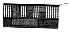
- FIG. 1shows a conventionally manufactured structure used in a semiconductor device.
- This structuregenerally represented as reference numeral 100 , is a single level structure, i.e., single wiring layer, shown for illustrative purposes; however, it should be readily understood by those of skill in the art that the structure shown and described herein can be a multilevel structure of several different layers. The methods of manufacturing described herein are equally applicable to such a multilevel structure.
- the structure 100 of FIG. 1includes a substrate 110 of any conventional material such as, for example silicon.
- the substratemay be an integrated circuit built up to a wiring level.
- An insulation layer 120is deposited on the substrate 110 using any known method such as, for example, plasma enhanced chemical vapor deposition (PECVD), chemical vapor deposition (CVD) or other processes.
- PECVDplasma enhanced chemical vapor deposition
- CVDchemical vapor deposition
- the insulation layer 120may be, for example: (i) undoped silicon glass (USG), (ii) USG and fluorosilicate glass (FSG), (iii) organo silicate glass (OSG), (iv) porous-OSG and OSG, (v) any combination of these materials or any other known dielectric material.
- the insulation layer 120is preferably either OSG or a layered structure of OSG and porous-OSG.
- One or more interconnects 130are formed in the insulation layer 120 .
- a diffusion barrier layer 135which may be SiC, SiN or other known material, as discussed herein, is deposited on the insulation layer 120 to protect the interconnects 130 .
- the diffusion barrier layer 135may additional act as an etch mask in subsequent processes.
- the diffusion barrier layer 135may be at a thickness in the range of 250 ⁇ to 500 ⁇ , or other thicknesses depending on the application.
- FIG. 2is representative of a first step of the method of the invention.
- a blockout patterned resist 140(supra lithographic mask) is deposited or formed on the diffusion barrier layer 135 .
- the blockout patterned resist 140is, in one implementation 2000 ⁇ to 1 micron in thickness and is deposited in any conventional manner.
- the blockout patterned resist 140may be any conventional photoresist material.
- the blockout patterned resist 140includes holes or features that are larger than the minimal resolution features; that is, in one implementation, the features of the blockout patterned resist 140 are larger than the spacings between the interconnects 130 .
- FIG. 3is representative of a second step of the invention.
- a block copolymer nanotemplate 150is formed over the blockout patterned resist 140 and portions of the diffusion barrier layer 135 .
- the block copolymer nanotemplate 150is a thin layer having features smaller than the minimal resolution features. In other words, the features of the block copolymer nanotemplate 150 are smaller, in one implementation, than the spacings between the interconnects 130 .
- the block copolymer nanotemplate 150may be a material which self assemblies itself into substantially uniformly shaped and spaced holes or features.
- the block copolymer nanotemplate 150may be a self assembled monolayer templated porous or permeable film.
- the block copolymer nanotemplate 150may be e-beam, uv or thermally cured. It should be further recognized that in implementations, the blockout pattern resist 140 may instead be formed over the block copolymer nanotemplate 150 .
- the holes of the block copolymer nanotemplate 150are about 20 nm in diameter with a spacing of about 20 nm therebetween. In other implementations, the spacings and diameter of the features may range from, for example, below 5 nm to 100 nm.
- the thickness of the block copolymer nanotemplate 150in one implementation, is approximately 20 nm and is made from an organic polymer matrix having a mesh of holes. It should be understood, though, that the thickness of the block copolymer nanotemplate 150 (and blockout resist) may vary depending on the thickness of the insulation layer, the required feature resolution and other factors, all of which can be ascertained by one of ordinary skill in the art in view of the description herein.
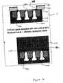
- FIG. 4shows an etching step of the invention.
- an etchin one implementation, using RIE is used to form channels 160 or nano columns between the interconnects 130 .
- the insulation layer 120may be deliberately eroded to form one or more nano column between adjacent interconnects. In some implementations, the insulation layer may be eroded to the substrate or lower layer level.
- the block copolymer nanotemplate 150may also begin to erode; however, the features of the block copolymer nanotemplate 150 are transferred to the diffusion barrier layer 135 , which will then act as the mask having the transferred features.
- An undercut below the interconnectsmay also be formed.
- small holes 135 ai.e., approximately equal to the channels 160 , remain at the surface of the insulation material 120 , basically corresponding to the size of the features of the block copolymer nanotemplate 150 .
- the holes 135 amay be on the order of 20 ⁇ to 200 ⁇ in diameter, for example.
- insulation material 120 amay be etched from the sidewalls of the interconnects 130 , but redeposited in further depositing steps.
- the sidewall material 120 amay be in the thickness range between 5 ⁇ and 200 ⁇ , with a thicker portion of the sidewall proximate to the block copolymer nanotemplate 150 or diffusion barrier layer 135 .
- the masks 130 and 150may be tuned to control the pattern to thus, for example, preclude gaps near via lands and the like.
- the channels 160may extend partially or completely through the insulation layer 120 , or the insulation layer near the sidewalls of the interconnects may be completely or substantially completely eroded. In this latter situation, deposition of insulation material near the sidewalls may be provided during a subsequent step of forming a higher interconnect layer.
- the RIEis an anisotropic etch, etching primarily straight down, in order to etch away the insulation to form the channels 160 .
- the RIE etchmay be followed by a wet clean process to remove any polymer residue resulting from the etching process.
- This cleaning chemistrymay contain an etchant to continue isotropic etching of the insulation layer to form an undercut below the interconnects ( FIG. 5 ).
- the etching of insulation layers comprising USG or FSGis relatively slow using dilute hydrofluoric acid (DHF).
- DHFdilute hydrofluoric acid
- the etch ratemay be 10 ⁇ to 20 ⁇ per minute at a H 2 O:HF ratio of 200:1.
- OSGhas a very low chemical etch rate in DHF, which is almost immeasurable.
- RIE with plasma O 2is used to provide more complete etch capabilities by oxidizing or “damaging” the first skin layer of the exposed OSG. Then, this damaged layer will etch very readily in this DHF.
- O 2there is the possibility of damaging the OSG insulation layer or diffusion layer. This damage can be corrected by providing another etch to the damaged portions.
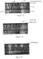
- FIG. 5represents an isotropic etching step to enlarge the nano columns into a single larger column 160 a than the original holes of the block copolymer nanotemplate 150 , in addition to providing an undercut to the formed channels.
- the RIEis changed by adding, for example, O 2 .
- the isotropic etchforms the undercuts 160 b , but should not etch away the entire area under the interconnects 130 .
- the etchingcan be tuned to provide for more extreme undercuts, depending on the desirability of the performance of the overall device; however, the undercut is preferably not performed under the entire area below the interconnects 130 . In one implementation, the undercuts will reduce vertical capacitance of wide lines.
- FIG. 6represents other processing steps of the invention.
- the block copolymer nanotemplate 150 and the blockout level patterned resist 140are etched or stripped, leaving behind the small holes 135 a .
- These masksmay have already eroded, entirely or partially, during the etching processes, thus leaving the diffusion barrier layer 135 as the mask.
- a wet etch processcan also be performed with solvent, DHF, or other acids to etch away any dielectric material which was previously damaged.
- the DHFis in a concentration from about 1000:1 to 10:1H 2 O:HF.
- backfill materialhaving a different dielectric constant and other properties, e.g., higher ductability, higher fracture toughness, etc., may be provided within the channels.
- a second insulation layer 170is then deposited on the thus formed structure using any conventional depositing method such as, for example, PEVCD.
- the second insulation layer 170may include a cap which will, after little deposition, cover the interconnects 130 (e.g., copper wires) and the diffusion barrier layer 135 , as well as forming pinch off areas 135 , in addition to sealing the channels.
- the cap layerwill, in embodiments, minimize topography.
- the pinch off portions 135 amay range between, for example, 20 ⁇ to 200 ⁇ , which are sub lithographic features. The pinch offs may act to minimize any level to level capacitance issues between adjacent layers.
- the material for the second layer of insulation layer 170may be, for example, (i) undoped silicon glass (USG), (ii) USG and fluorosilicate glass (FSG), (iii) organo silicate glass (OSG), (iv) porous-OSG and OSG, (v) any combination of these materials or any other known dielectric material.
- the insulation layer 170in one implementation, is preferably either OSG or a layered structure of OSG and porous-OSG, with the OSG acting as the cap for sealing the columns.
- FIG. 7shows a top view of the formed structure according to an aspect of the invention.
- blockout resist patterns 175may be formed using the blockout patterned resist 140 .
- the blockout resist patterns 175may be used to provide additional mechanical reinforcement to the formed structure at locations other than the formed channels.
- the blockout resist patterns 175may be formed over the scribe lanes or over the vias to provide additional strength and prevent pores in the vicinity of the sawing operation. It should be recognized that channels in the scribe lane may result in catastrophic failure due to shattering of the fragile material.
- the blockout resist patterns 175may also enable dielectric reinforcement with concurrent extreme cutout, and also to avoid or prevent gaps from forming near the via regions.
- the steps and structure of the inventionmay be repeated for higher level insulation layers.
- several insulation layers having vias, interconnects and channelsmay be formed using the methods of the invention.
- the effective dielectric constant of the insulation materialscan be reduced without significantly affecting the integrity, robustness and strength of the entire device.
- the methods of the inventioncan achieve a K eff of less than 2.0 with materials having a K eff of 2.7 or greater.
- porous materialscan be avoided for use in the insulation layer thus increasing the mechanical strength and thermal capabilities of the device, i.e., allowing the heat to transfer downward to the substrate.
- This structuremay also be formed by other methods described herein.
- FIGS. 9 though 14show another embodiment of the invention.
- FIG. 9is representative of a structure having two insulation layers 200 and 210 , of any type discussed above.
- the insulation layer 210may be SiO 2 , FSG, SiCOH, SiLK or other materials.
- the insulation layer 200includes an interconnect 220 and the insulation layer 210 includes a via 230 and several interconnects 240 .
- a dielectric cap, such as SiN, SiC, SiCOH, etc. (diffusion layer) 250is deposited over the insulation layer 210 and interconnects.
- the cap 250ranges, in one implementation, from 5 nm to 50 nm in thickness.
- An SiO 2 capmay be provided if the interconnect, e.g., copper wire, is capped. Multiple layers of these materials or any combination may also be used with the invention. It should be understood that this same or similar feature is applicable to other embodiments discussed herein.
- a blanket deposition layer 260 of SiO 2 followed by a deposition layer 270 of Au, Ag, In, Sn or Ga in the range from 5 nm to 50 nmis provided on the cap 250 .
- a blockout patterned resistmay be deposited between the deposition layers 260 and 270 , or alternatively above the deposition layer 270 .
- the blockout patterned resistshould be a supra lithographic mask for preventing the formation of gaps over larger areas of the device.
- the layer 270is treated, e.g., annealed, to cause agglomeration (i.e., beading) in order to form sub lithographic features in the range of 1 nm to 50 nm. In this manner, nano islands 270 a are formed from the layer 270 , which act as a mask for further processing steps.
- the layer 270is in the range of 1 nm to 50 nm in thickness and, in one implementation, in the range of 5 nm and 20 nm in thickness.
- poresare etched in layer 260 .
- This etchingmay be performed by RIE, in a conventional manner.
- the metal islands 270 aare stripped with a wet or dry etch, and etching continues with RIE into the layer 250 .
- An underlying hardmaskmay be used to protect the underlying structures during removal of the metal islands 270 a such as the cap 250 .
- This RIE etchingforms the channels or pores 250 a ( FIG. 12 ).
- Etchingcontinues into the SiO 2 layer 210 forming pores or nano channels 210 a substantially the same size as the sub lithographic features of layer 270 in the range of 1 nm to 50 nm.
- the RIE etchingis, in one implementation, an anisotropic etch.
- An dielectric cap layer 280such as SiO 2 , which can be deposited using PECVD or any known method, is deposited on the insulation layer 210 to seal the channels 250 a ( FIG. 14 ).
- the dielectric cap 280may have a thickness range of 5 nm to 50 nm, in one aspect of the invention. (Of course, other thicknesses, as with all other materials used herein, are also contemplated by the invention.)
- the dielectric cap 280may equally be other materials such as SiC, SiCOH or SiN, for example.
- the nano channelsmay be filled with a tough dielectric prior to the sealing with the capping dielectric layer. Pinch off sections may be formed in the capping dielectric layer 280 .
- a random hole pattern in resistmay be formed using e-beam, x-ray or EUV lithography.
- the resistsmask the regions where the dielectric is left behind and the vertical pores or columns are etched into the dielectric.
- a hardmasksuch as Nitride may be used underneath the resist if the dielectric is an organic material.
- a random hole pattern in a 2-phase polymer mask with porogenmay be utilized to form the pores.
- the polymeris applied and the porogen is then removed with a high temperature cure or with solvent, as is well known in the art. This will form the sub lithographic holes for further processing. There would be no need for optical lithographic exposure or photomask in this or other processes.
- the vertical pores or nano columnswould then be etched in the manner discussed above.
- a spin on film with fine metal particlessuch as a metal sol may be used to form the required holes, as may be represented by layer 270 .
- a single layer of fine metal particles from a solare deposited. This may be performed by pre-treating the layer 260 with a surfactant that forms a monolayer in the surface and attracts the sol particles to the surface to form a layer of the sol particles. That is, the layer would be burned away to leave metal particles on the surface which then could be used for the mask.
- a phase separable spin on solutionsuch as block copolymer can also be used as the mask.
- selective maskingcan be used to selectively add toughening to critical areas of the chip, such as discussed with reference to FIG. 7 .
Landscapes
- Engineering & Computer Science (AREA)
- Condensed Matter Physics & Semiconductors (AREA)
- General Physics & Mathematics (AREA)
- Physics & Mathematics (AREA)
- Power Engineering (AREA)
- Computer Hardware Design (AREA)
- Microelectronics & Electronic Packaging (AREA)
- Manufacturing & Machinery (AREA)
- Chemical & Material Sciences (AREA)
- Nanotechnology (AREA)
- Inorganic Chemistry (AREA)
- Composite Materials (AREA)
- Materials Engineering (AREA)
- Crystallography & Structural Chemistry (AREA)
- Internal Circuitry In Semiconductor Integrated Circuit Devices (AREA)
Abstract
Description
- The invention generally relates to a semiconductor device and method of manufacture and, more particularly, to a semiconductor device and method of manufacturing sub lithographic features within a dielectric material to reduce the effective dielectric constant of such material.
- To fabricate microelectronic semiconductor devices such as an integrated circuit (IC), many different layers of metal and insulation are selectively deposited on a silicon wafer. The insulation layers may be, for example, silicon dioxide, silicon oxynitride, fluorinated silicate glass (FSG) and the like. These insulation layers are deposited between the metal layers, i.e., interlevel dielectric (ILD) layers, and may act as electrical insulation therebetween or serve other known functions. These layers are typically deposited by any well known method such as, for example, plasma enhanced chemical vapor deposition (PECVD), chemical vapor deposition (CVD) or other processes.
- The metal layers are interconnected by metallization through vias etched in the intervening insulation layers. Additionally, interconnects are provided separately within the dielectric (insulation) layers. To accomplish this, the stacked layers of metal and insulation undergo photolithographic processing to provide a pattern consistent with a predetermined IC design. By way of example, the top layer of the structure may be covered with a photo resist layer of photo-reactive polymeric material for patterning via a mask. A photolithographic process using either visible or ultraviolet light is then directed through the mask onto the photo resist layer to expose it in the mask pattern. An antireflective coating (ARC) layer may be provided at the top portion of the wafer substrate to minimize reflection of light back to the photo resist layer for more uniform processing. The etching may be performed by anisotropic or isotropic etching as well as wet or dry etching, depending on the physical and chemical characteristics of the materials. Regardless of the fabrication process, to maximize the integration of the device components in very large scale integration (VLSI), it is necessary to increase the density of the components.
- Although silicon dioxide material has been used as an insulating material due to its thermal stability and mechanical strength, in recent years it has been found that better device performance may be achieved by using a lower dielectric constant material. By using a lower dielectric constant insulator material, a reduction in the capacitance of the structure can be achieved which, in turn, increases the device speed. However, use of organic low-k dielectric materials such as, for example, SiLK (manufactured by Dow Chemical Co., Midland, Mich.) tend to have lower mechanical strength than conventional dielectric materials such as, for example, silicon oxide. In some applications, it has been found that the following materials, in combination with other materials within a device, have a certain effective dielectric constant, such as, for example: (i) undoped silicon glass (USG) has a K of 4.1 and a Keffof approximately 4.3; (ii) USG and fluorosilicate glass (FSG) (K of 3.6) has bilayer Keffof approximately 3.8; (iii) organo silicate glass (OSG) has a K of 2.9 and has a Keffof approximately 3.0; and (iv) porous-OSG has a K of 2.2 and a bilayer of porous-OSG and OSG has a Keffof approximately 2.4.
- By building a device having a low-k dielectric or a hybrid low-k dielectric stack, the large intra-level line-to-line component of wiring capacitive coupling is reduced, thus maximizing the positive benefit of the low-k material while improving the overall robustness and reliability of the finished structure. The hybrid oxide/low-k dielectric stack structure is much more robust than an “all low-k” dielectric stack, which is known to be relatively more susceptible to via resistance degradation or via delamination due to thermal cycle stresses driven by the high CTE (coefficient of thermal expansion) of organic and semiorganic low-k dielectrics. However, the overall strength of the dielectric is considerably reduced at the lower dielectric constants.
- Nonetheless, even with the lower dielectric constant materials including, for example, a hybrid oxide/low-k dielectric stack structure, there is still the possibility to improve even further the electrical properties of the device by lowering the effective K (Keff) of a multilevel structure or a K of the dielectric material by forming voided channels within the dielectric material between the interconnects and vias. The channels are vacuum filled and have a dielectric constant of about 1. By using such channels, a higher dielectric constant dielectric material, itself, may be used to increase the overall strength of the structure without reducing the electric properties.
- In known systems, sub-resolution lithography processes have been used to create such channels. This typically consists of new manufacturing processes and tool sets which add to the overall cost of the fabrication of the semiconductor device. Also, in sub-resolution lithography processes, it is necessary to etch wide troughs in empty spaces which, in turn, cannot be pinched off by ILD PECVD deposition. Additionally, although the channels create low line-line capacitance, there remains a high level-level capacitance for wide lines. This, of course, affects the overall electrical properties of the device. Also, air gaps can occur near the vias from a higher level which creates the risk of plating bath or metal fill at these areas. Lastly, in known processes, there is also the requirement of providing an isotropic etch which may etch underneath the interconnect thus leaving it unsupported or floating and, thus degrading the entire structural and electrical performance of the device.
- The present invention is directed to solving these and other problems.
- In a first aspect of the invention, a method for manufacturing a structure includes providing a structure having an insulator layer with at least one interconnect and forming a sub lithographic template mask on the insulator layer. A selectively etching step is used for etching the insulator layer through the sub lithographic template mask to form sub lithographic features spanning to a sidewall of the at least one interconnect.
- In another aspect of the invention, the method includes providing a structure having an insulator layer with a plurality of interconnects and forming a blocking structure on the insulator layer. The method further includes forming a sub lithographic template mask on the blocking structure having sub lithographic features and selectively etching the blocking structure and the insulator layer through the sub lithographic template mask to form sub lithographic features in the insulator layer.
- In still another aspect of the invention, a semiconductor structure includes an insulator layer having at least one gap formed in the insulator layer spanning more than a minimum spacing of the interconnects.
FIG. 1 is representative of a beginning structure used with the invention;FIG. 2 is representative of a processing step in accordance with the invention;FIG. 3 is representative of a processing step in accordance with the invention;FIG. 4 is representative of a processing step in accordance with the invention;FIG. 5 is representative of a processing step in accordance with the invention;FIG. 6 is representative of processing steps in accordance with the invention (and the formed structure);FIG. 7 is a top view of the formed structure in accordance with the invention;FIG. 8 is a side cut away view of a multilayered structure formed in accordance with the invention;FIG. 9 is representative of a processing step in accordance with the invention;FIG. 10 is representative of a processing step in accordance with the invention;FIG. 11 is representative of a processing step in accordance with the invention;FIG. 12 is representative of a processing step in accordance with the invention;FIG. 13 is representative of a processing step in accordance with the invention; andFIG. 14 is representative of a processing step in accordance with the invention (and the formed structure).- This invention is directed to a semiconductor device and methods of manufacture for providing channels (or pores) in a dielectric (insulator) material to improve overall device performance. The methods of the invention do not require new manufacturing processes or tool sets nor do they introduce new materials into the final build and further avoid many of the shortcomings of sub-resolution photolithographic processes. Additionally, the methods of the invention are easily adaptable for use with any dielectric material, whether a hybrid structure or a material having a high dielectric constant. The invention, in one aspect, prevents floating interconnects and also, while decreasing the effective dielectric constant, Keff, may maintain the low level-level vertical capacitance of the interconnects. The overall device strength may also be maintained using the methods of the invention.
FIG. 1 shows a conventionally manufactured structure used in a semiconductor device. This structure, generally represented asreference numeral 100, is a single level structure, i.e., single wiring layer, shown for illustrative purposes; however, it should be readily understood by those of skill in the art that the structure shown and described herein can be a multilevel structure of several different layers. The methods of manufacturing described herein are equally applicable to such a multilevel structure.- The
structure 100 ofFIG. 1 includes asubstrate 110 of any conventional material such as, for example silicon. The substrate may be an integrated circuit built up to a wiring level. Aninsulation layer 120 is deposited on thesubstrate 110 using any known method such as, for example, plasma enhanced chemical vapor deposition (PECVD), chemical vapor deposition (CVD) or other processes. Theinsulation layer 120 may be, for example: (i) undoped silicon glass (USG), (ii) USG and fluorosilicate glass (FSG), (iii) organo silicate glass (OSG), (iv) porous-OSG and OSG, (v) any combination of these materials or any other known dielectric material. Theinsulation layer 120, in one implementation, is preferably either OSG or a layered structure of OSG and porous-OSG. One ormore interconnects 130 are formed in theinsulation layer 120. Adiffusion barrier layer 135 which may be SiC, SiN or other known material, as discussed herein, is deposited on theinsulation layer 120 to protect theinterconnects 130. Thediffusion barrier layer 135 may additional act as an etch mask in subsequent processes. Thediffusion barrier layer 135 may be at a thickness in the range of 250 Å to 500 Å, or other thicknesses depending on the application. FIG. 2 is representative of a first step of the method of the invention. In this step, a blockout patterned resist140 (supra lithographic mask) is deposited or formed on thediffusion barrier layer 135. The blockout patterned resist140 is, in one implementation 2000 Å to 1 micron in thickness and is deposited in any conventional manner. The blockout patterned resist140 may be any conventional photoresist material. The blockout patterned resist140 includes holes or features that are larger than the minimal resolution features; that is, in one implementation, the features of the blockout patterned resist140 are larger than the spacings between theinterconnects 130.FIG. 3 is representative of a second step of the invention. InFIG. 3 , ablock copolymer nanotemplate 150 is formed over the blockout patterned resist140 and portions of thediffusion barrier layer 135. Theblock copolymer nanotemplate 150 is a thin layer having features smaller than the minimal resolution features. In other words, the features of theblock copolymer nanotemplate 150 are smaller, in one implementation, than the spacings between theinterconnects 130. Theblock copolymer nanotemplate 150 may be a material which self assemblies itself into substantially uniformly shaped and spaced holes or features. For example, theblock copolymer nanotemplate 150 may be a self assembled monolayer templated porous or permeable film. Theblock copolymer nanotemplate 150 may be e-beam, uv or thermally cured. It should be further recognized that in implementations, the blockout pattern resist140 may instead be formed over theblock copolymer nanotemplate 150.- In one implementation, the holes of the
block copolymer nanotemplate 150 are about 20 nm in diameter with a spacing of about 20 nm therebetween. In other implementations, the spacings and diameter of the features may range from, for example, below 5 nm to 100 nm. The thickness of theblock copolymer nanotemplate 150, in one implementation, is approximately 20 nm and is made from an organic polymer matrix having a mesh of holes. It should be understood, though, that the thickness of the block copolymer nanotemplate150 (and blockout resist) may vary depending on the thickness of the insulation layer, the required feature resolution and other factors, all of which can be ascertained by one of ordinary skill in the art in view of the description herein. FIG. 4 shows an etching step of the invention. Now that theblock copolymer nanotemplate 150 and the diblock patterned resist140 are formed on the structure, an etch, in one implementation, using RIE is used to formchannels 160 or nano columns between theinterconnects 130. In this step, as theinsulator 150 is etched between the holes of theblock copolymer nanotemplate 150, theinsulation layer 120 may be deliberately eroded to form one or more nano column between adjacent interconnects. In some implementations, the insulation layer may be eroded to the substrate or lower layer level. In this step, since no etch process is infinitely selective, theblock copolymer nanotemplate 150 may also begin to erode; however, the features of theblock copolymer nanotemplate 150 are transferred to thediffusion barrier layer 135, which will then act as the mask having the transferred features. An undercut below the interconnects may also be formed.- As seen in
FIG. 4 , small holes135a, i.e., approximately equal to thechannels 160, remain at the surface of theinsulation material 120, basically corresponding to the size of the features of theblock copolymer nanotemplate 150. The holes135amay be on the order of 20 Å to 200 Å in diameter, for example. Additionally, during etching, insulation material120amay be etched from the sidewalls of theinterconnects 130, but redeposited in further depositing steps. In one implementation, the sidewall material120amay be in the thickness range between 5 Å and 200 Å, with a thicker portion of the sidewall proximate to theblock copolymer nanotemplate 150 ordiffusion barrier layer 135. It should be understood by those of skill in the art that themasks channels 160 may extend partially or completely through theinsulation layer 120, or the insulation layer near the sidewalls of the interconnects may be completely or substantially completely eroded. In this latter situation, deposition of insulation material near the sidewalls may be provided during a subsequent step of forming a higher interconnect layer. - The RIE, is an anisotropic etch, etching primarily straight down, in order to etch away the insulation to form the
channels 160. The RIE etch may be followed by a wet clean process to remove any polymer residue resulting from the etching process. This cleaning chemistry may contain an etchant to continue isotropic etching of the insulation layer to form an undercut below the interconnects (FIG. 5 ). The etching of insulation layers comprising USG or FSG is relatively slow using dilute hydrofluoric acid (DHF). For example, the etch rate may be 10 Å to 20 Å per minute at a H2O:HF ratio of 200:1. - On the other hand, OSG has a very low chemical etch rate in DHF, which is almost immeasurable. In OSG implementations, RIE with plasma O2is used to provide more complete etch capabilities by oxidizing or “damaging” the first skin layer of the exposed OSG. Then, this damaged layer will etch very readily in this DHF. However, when using O2, there is the possibility of damaging the OSG insulation layer or diffusion layer. This damage can be corrected by providing another etch to the damaged portions.
FIG. 5 represents an isotropic etching step to enlarge the nano columns into a singlelarger column 160athan the original holes of theblock copolymer nanotemplate 150, in addition to providing an undercut to the formed channels. In this step, the RIE is changed by adding, for example, O2. In this step, the isotropic etch forms the undercuts160b, but should not etch away the entire area under theinterconnects 130. Again, the etching can be tuned to provide for more extreme undercuts, depending on the desirability of the performance of the overall device; however, the undercut is preferably not performed under the entire area below theinterconnects 130. In one implementation, the undercuts will reduce vertical capacitance of wide lines.FIG. 6 represents other processing steps of the invention. For example, after the undercuts are formed, theblock copolymer nanotemplate 150 and the blockout level patterned resist140 are etched or stripped, leaving behind the small holes135a. These masks may have already eroded, entirely or partially, during the etching processes, thus leaving thediffusion barrier layer 135 as the mask. A wet etch process can also be performed with solvent, DHF, or other acids to etch away any dielectric material which was previously damaged. In one implementation, the DHF is in a concentration from about 1000:1 to 10:1H2O:HF. In an aspect of the invention, by widening thechannels 160, backfill material having a different dielectric constant and other properties, e.g., higher ductability, higher fracture toughness, etc., may be provided within the channels.- Still referring to
FIG. 6 , a second insulation layer170 is then deposited on the thus formed structure using any conventional depositing method such as, for example, PEVCD. The second insulation layer170 may include a cap which will, after little deposition, cover the interconnects130 (e.g., copper wires) and thediffusion barrier layer 135, as well as forming pinch offareas 135, in addition to sealing the channels. The cap layer will, in embodiments, minimize topography. The pinch off portions135amay range between, for example, 20 Å to 200 Å, which are sub lithographic features. The pinch offs may act to minimize any level to level capacitance issues between adjacent layers. - During the initial deposition of insulation material, the small size of the holes135asubstantially eliminates significant thickness of material from being deposited within the
columns 160. The material for the second layer of insulation layer170 may be, for example, (i) undoped silicon glass (USG), (ii) USG and fluorosilicate glass (FSG), (iii) organo silicate glass (OSG), (iv) porous-OSG and OSG, (v) any combination of these materials or any other known dielectric material. The insulation layer170, in one implementation, is preferably either OSG or a layered structure of OSG and porous-OSG, with the OSG acting as the cap for sealing the columns. FIG. 7 shows a top view of the formed structure according to an aspect of the invention. In this view, blockout resist patterns175 may be formed using the blockout patterned resist140. The blockout resist patterns175 may be used to provide additional mechanical reinforcement to the formed structure at locations other than the formed channels. By way of one example, the blockout resist patterns175 may be formed over the scribe lanes or over the vias to provide additional strength and prevent pores in the vicinity of the sawing operation. It should be recognized that channels in the scribe lane may result in catastrophic failure due to shattering of the fragile material. The blockout resist patterns175 may also enable dielectric reinforcement with concurrent extreme cutout, and also to avoid or prevent gaps from forming near the via regions.- It should be understood that the steps and structure of the invention, as described above, may be repeated for higher level insulation layers. Thus, as shown in
FIG. 7 , several insulation layers having vias, interconnects and channels may be formed using the methods of the invention. It should also be understood that by providing the channels, the effective dielectric constant of the insulation materials can be reduced without significantly affecting the integrity, robustness and strength of the entire device. In fact, the methods of the invention can achieve a Keffof less than 2.0 with materials having a Keffof 2.7 or greater. Additionally, by using the method of the invention, porous materials can be avoided for use in the insulation layer thus increasing the mechanical strength and thermal capabilities of the device, i.e., allowing the heat to transfer downward to the substrate. This structure may also be formed by other methods described herein. - FIGS.9 though14 show another embodiment of the invention.
FIG. 9 is representative of a structure having twoinsulation layers 200 and210, of any type discussed above. For example, theinsulation layer 210 may be SiO2, FSG, SiCOH, SiLK or other materials. The insulation layer200 includes aninterconnect 220 and theinsulation layer 210 includes a via230 andseveral interconnects 240. A dielectric cap, such as SiN, SiC, SiCOH, etc. (diffusion layer)250 is deposited over theinsulation layer 210 and interconnects. Thecap 250 ranges, in one implementation, from 5 nm to 50 nm in thickness. An SiO2cap may be provided if the interconnect, e.g., copper wire, is capped. Multiple layers of these materials or any combination may also be used with the invention. It should be understood that this same or similar feature is applicable to other embodiments discussed herein. - Referring now to
FIGS. 10 through 14 , ablanket deposition layer 260 of SiO2followed by adeposition layer 270 of Au, Ag, In, Sn or Ga in the range from 5 nm to 50 nm is provided on thecap 250. It should be understood that a blockout patterned resist may be deposited between the deposition layers260 and270, or alternatively above thedeposition layer 270. As in the previous embodiment, the blockout patterned resist should be a supra lithographic mask for preventing the formation of gaps over larger areas of the device. Metals which can easily dissolve in acids, acid salts and alkaline solutions such as Sn or In may be used in the invention in order to provide for easier removal at a later stage; however, other metals are also contemplated for use with this aspect of the invention. Thelayer 270 is treated, e.g., annealed, to cause agglomeration (i.e., beading) in order to form sub lithographic features in the range of 1 nm to 50 nm. In this manner, nano islands270aare formed from thelayer 270, which act as a mask for further processing steps. Thelayer 270 is in the range of 1 nm to 50 nm in thickness and, in one implementation, in the range of 5 nm and 20 nm in thickness. - In
FIG. 11 , pores are etched inlayer 260. This etching may be performed by RIE, in a conventional manner. The metal islands270aare stripped with a wet or dry etch, and etching continues with RIE into thelayer 250. An underlying hardmask may be used to protect the underlying structures during removal of the metal islands270asuch as thecap 250. This RIE etching forms the channels or pores250a(FIG. 12 ). Etching continues into the SiO2layer210 forming pores or nano channels210asubstantially the same size as the sub lithographic features oflayer 270 in the range of 1 nm to 50 nm. The RIE etching is, in one implementation, an anisotropic etch. - An
dielectric cap layer 280, such as SiO2, which can be deposited using PECVD or any known method, is deposited on theinsulation layer 210 to seal the channels250a(FIG. 14 ). Thedielectric cap 280 may have a thickness range of 5 nm to 50 nm, in one aspect of the invention. (Of course, other thicknesses, as with all other materials used herein, are also contemplated by the invention.) Thedielectric cap 280 may equally be other materials such as SiC, SiCOH or SiN, for example. In one embodiment, the nano channels may be filled with a tough dielectric prior to the sealing with the capping dielectric layer. Pinch off sections may be formed in the cappingdielectric layer 280. - In aspects of this embodiment, a random hole pattern in resist may be formed using e-beam, x-ray or EUV lithography. In this case, the resists mask the regions where the dielectric is left behind and the vertical pores or columns are etched into the dielectric. A hardmask such as Nitride may be used underneath the resist if the dielectric is an organic material.
- As a further alternative, a random hole pattern in a 2-phase polymer mask with porogen may be utilized to form the pores. To fabricate the mask, the polymer is applied and the porogen is then removed with a high temperature cure or with solvent, as is well known in the art. This will form the sub lithographic holes for further processing. There would be no need for optical lithographic exposure or photomask in this or other processes. The vertical pores or nano columns would then be etched in the manner discussed above.
- Alternatively, a spin on film with fine metal particles such as a metal sol may be used to form the required holes, as may be represented by
layer 270. In this process, a single layer of fine metal particles from a sol are deposited. This may be performed by pre-treating thelayer 260 with a surfactant that forms a monolayer in the surface and attracts the sol particles to the surface to form a layer of the sol particles. That is, the layer would be burned away to leave metal particles on the surface which then could be used for the mask. A phase separable spin on solution such as block copolymer can also be used as the mask. In addition, in this embodiment, selective masking can be used to selectively add toughening to critical areas of the chip, such as discussed with reference toFIG. 7 . - While the invention has been described in terms of embodiments, those skilled in the art will recognize that the invention can be practiced with modifications and in the spirit and scope of the appended claims.
Claims (57)
Priority Applications (8)
| Application Number | Priority Date | Filing Date | Title |
|---|---|---|---|
| US10/707,996US7405147B2 (en) | 2004-01-30 | 2004-01-30 | Device and methodology for reducing effective dielectric constant in semiconductor devices |
| CNB200510004272XACN100428422C (en) | 2004-01-30 | 2005-01-04 | Device and method for reducing effective dielectric constant in semiconductor devices |
| TW094101987ATWI355710B (en) | 2004-01-30 | 2005-01-24 | Device and methodology for reducing effective diel |
| JP2005021358AJP4378297B2 (en) | 2004-01-30 | 2005-01-28 | Method for manufacturing a semiconductor device having a low effective dielectric constant |
| US11/849,048US7592685B2 (en) | 2004-01-30 | 2007-08-31 | Device and methodology for reducing effective dielectric constant in semiconductor devices |
| US11/851,123US7892940B2 (en) | 2004-01-30 | 2007-09-06 | Device and methodology for reducing effective dielectric constant in semiconductor devices |
| US12/139,803US8129286B2 (en) | 2004-01-30 | 2008-06-16 | Reducing effective dielectric constant in semiconductor devices |
| US13/005,201US8343868B2 (en) | 2004-01-30 | 2011-01-12 | Device and methodology for reducing effective dielectric constant in semiconductor devices |
Applications Claiming Priority (1)
| Application Number | Priority Date | Filing Date | Title |
|---|---|---|---|
| US10/707,996US7405147B2 (en) | 2004-01-30 | 2004-01-30 | Device and methodology for reducing effective dielectric constant in semiconductor devices |
Related Child Applications (3)
| Application Number | Title | Priority Date | Filing Date |
|---|---|---|---|
| US11/849,048DivisionUS7592685B2 (en) | 2004-01-30 | 2007-08-31 | Device and methodology for reducing effective dielectric constant in semiconductor devices |
| US11/851,123DivisionUS7892940B2 (en) | 2004-01-30 | 2007-09-06 | Device and methodology for reducing effective dielectric constant in semiconductor devices |
| US12/139,803ContinuationUS8129286B2 (en) | 2004-01-30 | 2008-06-16 | Reducing effective dielectric constant in semiconductor devices |
Publications (2)
| Publication Number | Publication Date |
|---|---|
| US20050167838A1true US20050167838A1 (en) | 2005-08-04 |
| US7405147B2 US7405147B2 (en) | 2008-07-29 |
Family
ID=34807364
Family Applications (5)
| Application Number | Title | Priority Date | Filing Date |
|---|---|---|---|
| US10/707,996Expired - LifetimeUS7405147B2 (en) | 2004-01-30 | 2004-01-30 | Device and methodology for reducing effective dielectric constant in semiconductor devices |
| US11/849,048Expired - Fee RelatedUS7592685B2 (en) | 2004-01-30 | 2007-08-31 | Device and methodology for reducing effective dielectric constant in semiconductor devices |
| US11/851,123Expired - Fee RelatedUS7892940B2 (en) | 2004-01-30 | 2007-09-06 | Device and methodology for reducing effective dielectric constant in semiconductor devices |
| US12/139,803Active2026-02-07US8129286B2 (en) | 2004-01-30 | 2008-06-16 | Reducing effective dielectric constant in semiconductor devices |
| US13/005,201Expired - Fee RelatedUS8343868B2 (en) | 2004-01-30 | 2011-01-12 | Device and methodology for reducing effective dielectric constant in semiconductor devices |
Family Applications After (4)
| Application Number | Title | Priority Date | Filing Date |
|---|---|---|---|
| US11/849,048Expired - Fee RelatedUS7592685B2 (en) | 2004-01-30 | 2007-08-31 | Device and methodology for reducing effective dielectric constant in semiconductor devices |
| US11/851,123Expired - Fee RelatedUS7892940B2 (en) | 2004-01-30 | 2007-09-06 | Device and methodology for reducing effective dielectric constant in semiconductor devices |
| US12/139,803Active2026-02-07US8129286B2 (en) | 2004-01-30 | 2008-06-16 | Reducing effective dielectric constant in semiconductor devices |
| US13/005,201Expired - Fee RelatedUS8343868B2 (en) | 2004-01-30 | 2011-01-12 | Device and methodology for reducing effective dielectric constant in semiconductor devices |
Country Status (4)
| Country | Link |
|---|---|
| US (5) | US7405147B2 (en) |
| JP (1) | JP4378297B2 (en) |
| CN (1) | CN100428422C (en) |
| TW (1) | TWI355710B (en) |
Cited By (22)
| Publication number | Priority date | Publication date | Assignee | Title |
|---|---|---|---|---|
| US20080026541A1 (en)* | 2006-07-26 | 2008-01-31 | International Business Machines Corporation | Air-gap interconnect structures with selective cap |
| US20080038915A1 (en)* | 2004-01-30 | 2008-02-14 | International Business Machines Corporation | Device and methodology for reducing effective dielectric constant in semiconductor devices |
| FR2907598A1 (en)* | 2007-03-27 | 2008-04-25 | Commissariat Energie Atomique | Electronic integrated circuit fabricating method, involves forming etch mask in copolymer layer, forming another etch mask by etching dielectric material through former etch mask, and removing sacrificial material through latter etch mask |
| US20080102401A1 (en)* | 2006-10-31 | 2008-05-01 | International Business Machines Corporation | Si-CONTAINING POLYMERS FOR NANO-PATTERN DEVICE FABRICATION |
| US20080122106A1 (en)* | 2006-09-11 | 2008-05-29 | International Business Machines | Method to generate airgaps with a template first scheme and a self aligned blockout mask |
| US20080182402A1 (en)* | 2007-01-26 | 2008-07-31 | International Business Machines Corporation | Sub-lithographic interconnect patterning using self-assembling polymers |
| US20080217730A1 (en)* | 2007-03-07 | 2008-09-11 | Toshiharu Furukawa | Methods of forming gas dielectric and related structure |
| US20080314521A1 (en)* | 2005-11-30 | 2008-12-25 | Lam Research Corporation | Device with self aligned gaps for capacitance reduction |
| US20090001045A1 (en)* | 2007-06-27 | 2009-01-01 | International Business Machines Corporation | Methods of patterning self-assembly nano-structure and forming porous dielectric |
| US20090033362A1 (en)* | 2007-07-31 | 2009-02-05 | Dirk Manger | Method for Forming a Structure on a Substrate and Device |
| US20090117360A1 (en)* | 2007-11-01 | 2009-05-07 | International Business Machines Corporation | Self-assembled material pattern transfer contrast enhancement |
| US20090140428A1 (en)* | 2007-12-03 | 2009-06-04 | International Business Machines Corporation | Air gap structure having protective metal silicide pads on a metal feature |
| US20090140380A1 (en)* | 2005-11-30 | 2009-06-04 | Lam Research Corporation | Device with gaps for capacitance reduction |
| US20090302475A1 (en)* | 2008-02-18 | 2009-12-10 | Hayato Korogi | Semiconductor device and manufacturing method thereof |
| US20100219534A1 (en)* | 2009-02-27 | 2010-09-02 | Robert Seidel | Microstructure device including a metallization structure with self-aligned air gaps and refilled air gap exclusion zones |
| US20100294740A1 (en)* | 2009-05-19 | 2010-11-25 | International Business Machines Corporation | Directed self-assembly of block copolymers using segmented prepatterns |
| US20100297847A1 (en)* | 2009-05-22 | 2010-11-25 | International Business Machines Corporation | Method of forming sub-lithographic features using directed self-assembly of polymers |
| US7939446B1 (en) | 2009-11-11 | 2011-05-10 | International Business Machines Corporation | Process for reversing tone of patterns on integerated circuit and structural process for nanoscale fabrication |
| EP2047505A4 (en)* | 2006-07-11 | 2011-10-05 | Ibm | An interconnect structure with dielectric air gaps |
| US20130134590A1 (en)* | 2010-02-05 | 2013-05-30 | International Business Machines Corporation | Formation of air gap with protection of metal lines |
| US20130193551A1 (en)* | 2009-01-20 | 2013-08-01 | International Business Machines Corporation | Structure with self aligned resist layer on an interconnect surface and method of making same |
| US9105634B2 (en)* | 2012-06-29 | 2015-08-11 | Taiwan Semiconductor Manufacturing Company, Ltd. | Voids in interconnect structures and methods for forming the same |
Families Citing this family (62)
| Publication number | Priority date | Publication date | Assignee | Title |
|---|---|---|---|---|
| US7708924B2 (en)* | 2005-07-21 | 2010-05-04 | Asml Netherlands B.V. | Imprint lithography |
| US7692771B2 (en)* | 2005-05-27 | 2010-04-06 | Asml Netherlands B.V. | Imprint lithography |
| US7629225B2 (en)* | 2005-06-13 | 2009-12-08 | Infineon Technologies Ag | Methods of manufacturing semiconductor devices and structures thereof |
| US7544608B2 (en)* | 2006-07-19 | 2009-06-09 | International Business Machines Corporation | Porous and dense hybrid interconnect structure and method of manufacture |
| US7592247B2 (en)* | 2006-10-04 | 2009-09-22 | International Business Machines Corporation | Sub-lithographic local interconnects, and methods for forming same |
| US7544578B2 (en)* | 2007-01-03 | 2009-06-09 | International Business Machines Corporation | Structure and method for stochastic integrated circuit personalization |
| US7871923B2 (en)* | 2007-01-26 | 2011-01-18 | Taiwan Semiconductor Maufacturing Company, Ltd. | Self-aligned air-gap in interconnect structures |
| US8083953B2 (en) | 2007-03-06 | 2011-12-27 | Micron Technology, Inc. | Registered structure formation via the application of directed thermal energy to diblock copolymer films |
| US8557128B2 (en) | 2007-03-22 | 2013-10-15 | Micron Technology, Inc. | Sub-10 nm line features via rapid graphoepitaxial self-assembly of amphiphilic monolayers |
| US8173537B1 (en) | 2007-03-29 | 2012-05-08 | Novellus Systems, Inc. | Methods for reducing UV and dielectric diffusion barrier interaction |
| US8097175B2 (en)* | 2008-10-28 | 2012-01-17 | Micron Technology, Inc. | Method for selectively permeating a self-assembled block copolymer, method for forming metal oxide structures, method for forming a metal oxide pattern, and method for patterning a semiconductor structure |
| US8294139B2 (en)* | 2007-06-21 | 2012-10-23 | Micron Technology, Inc. | Multilayer antireflection coatings, structures and devices including the same and methods of making the same |
| US7959975B2 (en) | 2007-04-18 | 2011-06-14 | Micron Technology, Inc. | Methods of patterning a substrate |
| US8372295B2 (en) | 2007-04-20 | 2013-02-12 | Micron Technology, Inc. | Extensions of self-assembled structures to increased dimensions via a “bootstrap” self-templating method |
| JP2008294335A (en)* | 2007-05-28 | 2008-12-04 | Panasonic Corp | Manufacturing method of semiconductor device |
| US8404124B2 (en) | 2007-06-12 | 2013-03-26 | Micron Technology, Inc. | Alternating self-assembling morphologies of diblock copolymers controlled by variations in surfaces |
| JP2008311585A (en)* | 2007-06-18 | 2008-12-25 | Elpida Memory Inc | Wiring structure, semiconductor device, and their manufacturing methods |
| US8080615B2 (en) | 2007-06-19 | 2011-12-20 | Micron Technology, Inc. | Crosslinkable graft polymer non-preferentially wetted by polystyrene and polyethylene oxide |
| US20090093100A1 (en)* | 2007-10-09 | 2009-04-09 | Li-Qun Xia | Method for forming an air gap in multilevel interconnect structure |
| JP2009094378A (en)* | 2007-10-11 | 2009-04-30 | Panasonic Corp | Semiconductor device and manufacturing method thereof |
| US8083958B2 (en)* | 2007-12-05 | 2011-12-27 | International Business Machines Corporation | Patterning method using a combination of photolithography and copolymer self-assemblying lithography techniques |
| US8999492B2 (en) | 2008-02-05 | 2015-04-07 | Micron Technology, Inc. | Method to produce nanometer-sized features with directed assembly of block copolymers |
| US8101261B2 (en) | 2008-02-13 | 2012-01-24 | Micron Technology, Inc. | One-dimensional arrays of block copolymer cylinders and applications thereof |
| US8425982B2 (en) | 2008-03-21 | 2013-04-23 | Micron Technology, Inc. | Methods of improving long range order in self-assembly of block copolymer films with ionic liquids |
| US8426313B2 (en) | 2008-03-21 | 2013-04-23 | Micron Technology, Inc. | Thermal anneal of block copolymer films with top interface constrained to wet both blocks with equal preference |
| US8124522B1 (en)* | 2008-04-11 | 2012-02-28 | Novellus Systems, Inc. | Reducing UV and dielectric diffusion barrier interaction through the modulation of optical properties |
| US8114301B2 (en) | 2008-05-02 | 2012-02-14 | Micron Technology, Inc. | Graphoepitaxial self-assembly of arrays of downward facing half-cylinders |
| TWI407491B (en)* | 2008-05-09 | 2013-09-01 | Advanced Optoelectronic Tech | Method for separating semiconductor and substrate |
| JP5173863B2 (en)* | 2009-01-20 | 2013-04-03 | パナソニック株式会社 | Semiconductor device and manufacturing method thereof |
| US8247332B2 (en) | 2009-12-04 | 2012-08-21 | Novellus Systems, Inc. | Hardmask materials |
| US8456009B2 (en)* | 2010-02-18 | 2013-06-04 | Taiwan Semiconductor Manufacturing Company, Ltd. | Semiconductor structure having an air-gap region and a method of manufacturing the same |
| US8502329B2 (en)* | 2011-09-01 | 2013-08-06 | Solid State System Co., Ltd. | Micro-electro-mechanical systems (MEMS) device and method for fabricating the same |
| CN103094191B (en)* | 2011-11-01 | 2015-04-15 | 中芯国际集成电路制造(上海)有限公司 | Method of reducing dielectric constant of inter-lamination dielectric layer |
| US8900963B2 (en) | 2011-11-02 | 2014-12-02 | Micron Technology, Inc. | Methods of forming semiconductor device structures, and related structures |
| CN103165522B (en)* | 2011-12-15 | 2015-01-21 | 中芯国际集成电路制造(上海)有限公司 | Semiconductor structure and forming method of semiconductor structure |
| US10211310B2 (en) | 2012-06-12 | 2019-02-19 | Novellus Systems, Inc. | Remote plasma based deposition of SiOC class of films |
| US9234276B2 (en) | 2013-05-31 | 2016-01-12 | Novellus Systems, Inc. | Method to obtain SiC class of films of desired composition and film properties |
| US10832904B2 (en) | 2012-06-12 | 2020-11-10 | Lam Research Corporation | Remote plasma based deposition of oxygen doped silicon carbide films |
| US10325773B2 (en) | 2012-06-12 | 2019-06-18 | Novellus Systems, Inc. | Conformal deposition of silicon carbide films |
| CN102751237A (en)* | 2012-07-03 | 2012-10-24 | 上海华力微电子有限公司 | Manufacturing method of metal interconnection structure |
| US8715917B2 (en) | 2012-10-04 | 2014-05-06 | International Business Machines Corporation | Simultaneous photoresist development and neutral polymer layer formation |
| US9087699B2 (en) | 2012-10-05 | 2015-07-21 | Micron Technology, Inc. | Methods of forming an array of openings in a substrate, and related methods of forming a semiconductor device structure |
| US9337068B2 (en) | 2012-12-18 | 2016-05-10 | Lam Research Corporation | Oxygen-containing ceramic hard masks and associated wet-cleans |
| US8921167B2 (en) | 2013-01-02 | 2014-12-30 | International Business Machines Corporation | Modified via bottom for BEOL via efuse |
| US8993404B2 (en)* | 2013-01-23 | 2015-03-31 | Intel Corporation | Metal-insulator-metal capacitor formation techniques |
| CN104022069B (en)* | 2013-02-28 | 2017-09-22 | 中芯国际集成电路制造(上海)有限公司 | Semiconductor structure and forming method thereof |
| US8859433B2 (en)* | 2013-03-11 | 2014-10-14 | International Business Machines Corporation | DSA grapho-epitaxy process with etch stop material |
| US9229328B2 (en) | 2013-05-02 | 2016-01-05 | Micron Technology, Inc. | Methods of forming semiconductor device structures, and related semiconductor device structures |
| US10297442B2 (en) | 2013-05-31 | 2019-05-21 | Lam Research Corporation | Remote plasma based deposition of graded or multi-layered silicon carbide film |
| US8901621B1 (en) | 2013-06-18 | 2014-12-02 | International Business Machines Corporation | Nanochannel process and structure for bio-detection |
| US9177795B2 (en) | 2013-09-27 | 2015-11-03 | Micron Technology, Inc. | Methods of forming nanostructures including metal oxides |
| FR3021321B1 (en)* | 2014-05-26 | 2016-06-03 | Commissariat Energie Atomique | METHOD OF REALIZING PATTERNS BY SELF-ASSEMBLING BLOCK COPOLYMERS |
| US20160314964A1 (en) | 2015-04-21 | 2016-10-27 | Lam Research Corporation | Gap fill using carbon-based films |
| US10068844B2 (en)* | 2015-09-30 | 2018-09-04 | Taiwan Semiconductor Manufacturing Company, Ltd. | Integrated fan-out structure and method of forming |
| US9449871B1 (en) | 2015-11-18 | 2016-09-20 | International Business Machines Corporation | Hybrid airgap structure with oxide liner |
| WO2017105447A1 (en)* | 2015-12-16 | 2017-06-22 | Intel Corporation | Methods and apparatuses to provide ordered porosity |
| US10002787B2 (en) | 2016-11-23 | 2018-06-19 | Lam Research Corporation | Staircase encapsulation in 3D NAND fabrication |
| US9837270B1 (en) | 2016-12-16 | 2017-12-05 | Lam Research Corporation | Densification of silicon carbide film using remote plasma treatment |
| KR102594413B1 (en)* | 2018-03-30 | 2023-10-27 | 삼성전자주식회사 | Semiconductor devices |
| US11355430B2 (en)* | 2019-12-18 | 2022-06-07 | Taiwan Semiconductor Manufacturing Company, Ltd. | Capping layer overlying dielectric structure to increase reliability |
| CN113013141A (en) | 2019-12-18 | 2021-06-22 | 台湾积体电路制造股份有限公司 | Semiconductor structure |
| US20230402317A1 (en)* | 2022-06-09 | 2023-12-14 | Globalfoundries Singapore Pte. Ltd. | Structure including discrete dielectric member for protecting first air gap during forming of second air gap |
Citations (11)
| Publication number | Priority date | Publication date | Assignee | Title |
|---|---|---|---|---|
| US6265321B1 (en)* | 2000-04-17 | 2001-07-24 | Chartered Semiconductor Manufacturing Ltd. | Air bridge process for forming air gaps |
| US20020016058A1 (en)* | 2000-06-15 | 2002-02-07 | Bin Zhao | Microelectronic air-gap structures and methods of forming the same |
| US6346484B1 (en)* | 2000-08-31 | 2002-02-12 | International Business Machines Corporation | Method for selective extraction of sacrificial place-holding material used in fabrication of air gap-containing interconnect structures |
| US6358813B1 (en)* | 2000-11-15 | 2002-03-19 | International Business Machines Corporation | Method for increasing the capacitance of a semiconductor capacitors |
| US20020061633A1 (en)* | 2000-05-15 | 2002-05-23 | Marsh Eugene P. | Method of fabricating an SrRuO3 film |
| US20020061646A1 (en)* | 2000-11-21 | 2002-05-23 | Cornell Research Foundation, Inc. | Embedded metal nanocrystals |
| US6451712B1 (en)* | 2000-12-18 | 2002-09-17 | International Business Machines Corporation | Method for forming a porous dielectric material layer in a semiconductor device and device formed |
| US6495479B1 (en)* | 2000-05-05 | 2002-12-17 | Honeywell International, Inc. | Simplified method to produce nanoporous silicon-based films |
| US20030073302A1 (en)* | 2001-10-12 | 2003-04-17 | Reflectivity, Inc., A California Corporation | Methods for formation of air gap interconnects |
| US20080038923A1 (en)* | 2004-01-30 | 2008-02-14 | International Business Machines Corporation | Device and methodology for reducing effective dielectric constant in semiconductor devices |
| US20080093743A1 (en)* | 2006-10-19 | 2008-04-24 | International Business Machines Corporation | Sub-lithographic nano interconnect structures, and method for forming same |
Family Cites Families (36)
| Publication number | Priority date | Publication date | Assignee | Title |
|---|---|---|---|---|
| US4650544A (en)* | 1985-04-19 | 1987-03-17 | Advanced Micro Devices, Inc. | Shallow groove capacitor fabrication method |
| US5204280A (en)* | 1992-04-09 | 1993-04-20 | International Business Machines Corporation | Process for fabricating multiple pillars inside a dram trench for increased capacitor surface |
| US5538592A (en)* | 1994-07-22 | 1996-07-23 | International Business Machines Corporation | Non-random sub-lithography vertical stack capacitor |
| US5869880A (en)* | 1995-12-29 | 1999-02-09 | International Business Machines Corporation | Structure and fabrication method for stackable, air-gap-containing low epsilon dielectric layers |
| US5759913A (en)* | 1996-06-05 | 1998-06-02 | Advanced Micro Devices, Inc. | Method of formation of an air gap within a semiconductor dielectric by solvent desorption |
| US5695810A (en) | 1996-11-20 | 1997-12-09 | Cornell Research Foundation, Inc. | Use of cobalt tungsten phosphide as a barrier material for copper metallization |
| JP3623061B2 (en)* | 1996-12-12 | 2005-02-23 | 株式会社ルネサステクノロジ | Semiconductor device and manufacturing method thereof |
| JP2957543B1 (en)* | 1998-04-13 | 1999-10-04 | 九州日本電気株式会社 | Semiconductor device and manufacturing method thereof |
| US6346584B1 (en)* | 1999-09-09 | 2002-02-12 | Univation Technologies, Llc | Catalyst modifiers and their use in the polymerization of olefins(s) |
| US6214496B1 (en) | 1999-03-29 | 2001-04-10 | Infineon Technologies North America Corp. | Method for reducing corner rounding in mask fabrication utilizing elliptical energy beam |
| JP3461761B2 (en) | 1999-08-16 | 2003-10-27 | 松下電器産業株式会社 | Method for manufacturing semiconductor device |
| JP3314762B2 (en) | 1999-08-19 | 2002-08-12 | 日本電気株式会社 | Electron beam exposure mask, electron beam exposure method using the same, electron beam exposure apparatus, and device manufacturing method |
| US6498399B2 (en)* | 1999-09-08 | 2002-12-24 | Alliedsignal Inc. | Low dielectric-constant dielectric for etchstop in dual damascene backend of integrated circuits |
| US6153935A (en) | 1999-09-30 | 2000-11-28 | International Business Machines Corporation | Dual etch stop/diffusion barrier for damascene interconnects |
| JP3979791B2 (en) | 2000-03-08 | 2007-09-19 | 株式会社ルネサステクノロジ | Semiconductor device and manufacturing method thereof |
| US6387818B1 (en)* | 2000-07-21 | 2002-05-14 | Advanced Micro Devices, Inc. | Method of porous dielectric formation with anodic template |
| JP4252237B2 (en) | 2000-12-06 | 2009-04-08 | 株式会社アルバック | Ion implantation apparatus and ion implantation method |
| US6376366B1 (en)* | 2001-05-21 | 2002-04-23 | Taiwan Semiconductor Manufacturing Company | Partial hard mask open process for hard mask dual damascene etch |
| TW544806B (en)* | 2001-05-30 | 2003-08-01 | Asahi Glass Co Ltd | Low dielectric constant insulating film, method of forming it, and electric circuit using it |
| JP4953523B2 (en)* | 2001-06-29 | 2012-06-13 | ローム株式会社 | Semiconductor device and manufacturing method thereof |
| JP2003258095A (en)* | 2002-03-06 | 2003-09-12 | Sony Corp | Insulating film on base and method for manufacturing the same |
| JP2003347401A (en) | 2002-05-30 | 2003-12-05 | Mitsubishi Electric Corp | Semiconductor device having multilayer wiring structure and its manufacturing method |
| US6838354B2 (en) | 2002-12-20 | 2005-01-04 | Freescale Semiconductor, Inc. | Method for forming a passivation layer for air gap formation |
| US7087532B2 (en)* | 2004-09-30 | 2006-08-08 | International Business Machines Corporation | Formation of controlled sublithographic structures |
| US7670895B2 (en)* | 2006-04-24 | 2010-03-02 | Freescale Semiconductor, Inc | Process of forming an electronic device including a semiconductor layer and another layer adjacent to an opening within the semiconductor layer |
| US7528078B2 (en)* | 2006-05-12 | 2009-05-05 | Freescale Semiconductor, Inc. | Process of forming electronic device including a densified nitride layer adjacent to an opening within a semiconductor layer |
| US20080026541A1 (en)* | 2006-07-26 | 2008-01-31 | International Business Machines Corporation | Air-gap interconnect structures with selective cap |
| US7863150B2 (en)* | 2006-09-11 | 2011-01-04 | International Business Machines Corporation | Method to generate airgaps with a template first scheme and a self aligned blockout mask |
| US7560222B2 (en)* | 2006-10-31 | 2009-07-14 | International Business Machines Corporation | Si-containing polymers for nano-pattern device fabrication |
| TW200834968A (en)* | 2007-02-13 | 2008-08-16 | Harvatek Corp | Method of making light-emitting diode structure with high heat dissipation effect and structure made thereby |
| US7741721B2 (en)* | 2007-07-31 | 2010-06-22 | International Business Machines Corporation | Electrical fuses and resistors having sublithographic dimensions |
| US7879728B2 (en)* | 2008-01-23 | 2011-02-01 | International Business Machines Corporation | Sub-lithographic printing method |
| US7943480B2 (en)* | 2008-02-12 | 2011-05-17 | International Business Machines Corporation | Sub-lithographic dimensioned air gap formation and related structure |
| US8227336B2 (en)* | 2009-01-20 | 2012-07-24 | International Business Machines Corporation | Structure with self aligned resist layer on an interconnect surface and method of making same |
| US8247904B2 (en)* | 2009-08-13 | 2012-08-21 | International Business Machines Corporation | Interconnection between sublithographic-pitched structures and lithographic-pitched structures |
| US8120179B2 (en)* | 2009-11-10 | 2012-02-21 | International Business Machines Corporation | Air gap interconnect structures and methods for forming the same |
- 2004
- 2004-01-30USUS10/707,996patent/US7405147B2/ennot_activeExpired - Lifetime
- 2005
- 2005-01-04CNCNB200510004272XApatent/CN100428422C/ennot_activeExpired - Fee Related
- 2005-01-24TWTW094101987Apatent/TWI355710B/ennot_activeIP Right Cessation
- 2005-01-28JPJP2005021358Apatent/JP4378297B2/ennot_activeExpired - Lifetime
- 2007
- 2007-08-31USUS11/849,048patent/US7592685B2/ennot_activeExpired - Fee Related
- 2007-09-06USUS11/851,123patent/US7892940B2/ennot_activeExpired - Fee Related
- 2008
- 2008-06-16USUS12/139,803patent/US8129286B2/enactiveActive
- 2011
- 2011-01-12USUS13/005,201patent/US8343868B2/ennot_activeExpired - Fee Related
Patent Citations (16)
| Publication number | Priority date | Publication date | Assignee | Title |
|---|---|---|---|---|
| US6265321B1 (en)* | 2000-04-17 | 2001-07-24 | Chartered Semiconductor Manufacturing Ltd. | Air bridge process for forming air gaps |
| US6495479B1 (en)* | 2000-05-05 | 2002-12-17 | Honeywell International, Inc. | Simplified method to produce nanoporous silicon-based films |
| US20020061633A1 (en)* | 2000-05-15 | 2002-05-23 | Marsh Eugene P. | Method of fabricating an SrRuO3 film |
| US20020016058A1 (en)* | 2000-06-15 | 2002-02-07 | Bin Zhao | Microelectronic air-gap structures and methods of forming the same |
| US6509623B2 (en)* | 2000-06-15 | 2003-01-21 | Newport Fab, Llc | Microelectronic air-gap structures and methods of forming the same |
| US6346484B1 (en)* | 2000-08-31 | 2002-02-12 | International Business Machines Corporation | Method for selective extraction of sacrificial place-holding material used in fabrication of air gap-containing interconnect structures |
| US20020058394A1 (en)* | 2000-11-15 | 2002-05-16 | International Business Machines Corporation | Semiconductor capacitors |
| US6506660B2 (en)* | 2000-11-15 | 2003-01-14 | International Business Machines Corporation | Semiconductor with nanoscale features |
| US6358813B1 (en)* | 2000-11-15 | 2002-03-19 | International Business Machines Corporation | Method for increasing the capacitance of a semiconductor capacitors |
| US20020061646A1 (en)* | 2000-11-21 | 2002-05-23 | Cornell Research Foundation, Inc. | Embedded metal nanocrystals |
| US20020192949A1 (en)* | 2000-11-21 | 2002-12-19 | Cornell Research Foundation, Inc. | Embedded metal nanocrystals |
| US6451712B1 (en)* | 2000-12-18 | 2002-09-17 | International Business Machines Corporation | Method for forming a porous dielectric material layer in a semiconductor device and device formed |
| US20030073302A1 (en)* | 2001-10-12 | 2003-04-17 | Reflectivity, Inc., A California Corporation | Methods for formation of air gap interconnects |
| US20080038923A1 (en)* | 2004-01-30 | 2008-02-14 | International Business Machines Corporation | Device and methodology for reducing effective dielectric constant in semiconductor devices |
| US20080038915A1 (en)* | 2004-01-30 | 2008-02-14 | International Business Machines Corporation | Device and methodology for reducing effective dielectric constant in semiconductor devices |
| US20080093743A1 (en)* | 2006-10-19 | 2008-04-24 | International Business Machines Corporation | Sub-lithographic nano interconnect structures, and method for forming same |
Cited By (48)
| Publication number | Priority date | Publication date | Assignee | Title |
|---|---|---|---|---|
| US20080254630A1 (en)* | 2004-01-30 | 2008-10-16 | International Business Machines Corporation | Device and methodology for reducing effective dielectric constant in semiconductor devices |
| US20080038915A1 (en)* | 2004-01-30 | 2008-02-14 | International Business Machines Corporation | Device and methodology for reducing effective dielectric constant in semiconductor devices |
| US20080038923A1 (en)* | 2004-01-30 | 2008-02-14 | International Business Machines Corporation | Device and methodology for reducing effective dielectric constant in semiconductor devices |
| US20110111590A1 (en)* | 2004-01-30 | 2011-05-12 | International Business Machines Corporation | Device and methodology for reducing effective dielectric constant in semiconductor devices |
| US8129286B2 (en) | 2004-01-30 | 2012-03-06 | International Business Machines Corporation | Reducing effective dielectric constant in semiconductor devices |
| US7892940B2 (en)* | 2004-01-30 | 2011-02-22 | International Business Machines Corporation | Device and methodology for reducing effective dielectric constant in semiconductor devices |
| US7405147B2 (en)* | 2004-01-30 | 2008-07-29 | International Business Machines Corporation | Device and methodology for reducing effective dielectric constant in semiconductor devices |
| US7592685B2 (en) | 2004-01-30 | 2009-09-22 | International Business Machines Corporation | Device and methodology for reducing effective dielectric constant in semiconductor devices |
| US8343868B2 (en)* | 2004-01-30 | 2013-01-01 | International Business Machines Corporation | Device and methodology for reducing effective dielectric constant in semiconductor devices |
| US8187412B2 (en) | 2005-11-30 | 2012-05-29 | Lam Research Corporation; | Apparatus for providing device with gaps for capacitance reduction |
| US20080314521A1 (en)* | 2005-11-30 | 2008-12-25 | Lam Research Corporation | Device with self aligned gaps for capacitance reduction |
| US8866202B2 (en)* | 2005-11-30 | 2014-10-21 | Lam Research Corporation | Device with gaps for capacitance reduction |
| US8172980B2 (en) | 2005-11-30 | 2012-05-08 | Lam Research Corporation | Device with self aligned gaps for capacitance reduction |
| US20090140380A1 (en)* | 2005-11-30 | 2009-06-04 | Lam Research Corporation | Device with gaps for capacitance reduction |
| EP2047505A4 (en)* | 2006-07-11 | 2011-10-05 | Ibm | An interconnect structure with dielectric air gaps |
| US20080026541A1 (en)* | 2006-07-26 | 2008-01-31 | International Business Machines Corporation | Air-gap interconnect structures with selective cap |
| US20080122106A1 (en)* | 2006-09-11 | 2008-05-29 | International Business Machines | Method to generate airgaps with a template first scheme and a self aligned blockout mask |
| US20110163446A1 (en)* | 2006-09-11 | 2011-07-07 | International Business Machines Corporation | Method to generate airgaps with a template first scheme and a self aligned blockout mask and structure |
| US7863150B2 (en) | 2006-09-11 | 2011-01-04 | International Business Machines Corporation | Method to generate airgaps with a template first scheme and a self aligned blockout mask |
| US7560222B2 (en) | 2006-10-31 | 2009-07-14 | International Business Machines Corporation | Si-containing polymers for nano-pattern device fabrication |
| US20080102401A1 (en)* | 2006-10-31 | 2008-05-01 | International Business Machines Corporation | Si-CONTAINING POLYMERS FOR NANO-PATTERN DEVICE FABRICATION |
| US20080182402A1 (en)* | 2007-01-26 | 2008-07-31 | International Business Machines Corporation | Sub-lithographic interconnect patterning using self-assembling polymers |
| US7767099B2 (en)* | 2007-01-26 | 2010-08-03 | International Business Machines Corporaiton | Sub-lithographic interconnect patterning using self-assembling polymers |
| US20080217730A1 (en)* | 2007-03-07 | 2008-09-11 | Toshiharu Furukawa | Methods of forming gas dielectric and related structure |
| FR2907598A1 (en)* | 2007-03-27 | 2008-04-25 | Commissariat Energie Atomique | Electronic integrated circuit fabricating method, involves forming etch mask in copolymer layer, forming another etch mask by etching dielectric material through former etch mask, and removing sacrificial material through latter etch mask |
| US20090001045A1 (en)* | 2007-06-27 | 2009-01-01 | International Business Machines Corporation | Methods of patterning self-assembly nano-structure and forming porous dielectric |
| US20090033362A1 (en)* | 2007-07-31 | 2009-02-05 | Dirk Manger | Method for Forming a Structure on a Substrate and Device |
| US7737049B2 (en) | 2007-07-31 | 2010-06-15 | Qimonda Ag | Method for forming a structure on a substrate and device |
| US20090117360A1 (en)* | 2007-11-01 | 2009-05-07 | International Business Machines Corporation | Self-assembled material pattern transfer contrast enhancement |
| US7884477B2 (en) | 2007-12-03 | 2011-02-08 | International Business Machines Corporation | Air gap structure having protective metal silicide pads on a metal feature |
| US20110092067A1 (en)* | 2007-12-03 | 2011-04-21 | International Business Machines Corporation | Air gap structure having protective metal silicide pads on a metal feature |
| US8003520B2 (en) | 2007-12-03 | 2011-08-23 | International Business Machines Corporation | Air gap structure having protective metal silicide pads on a metal feature |
| US20090140428A1 (en)* | 2007-12-03 | 2009-06-04 | International Business Machines Corporation | Air gap structure having protective metal silicide pads on a metal feature |
| US20090302475A1 (en)* | 2008-02-18 | 2009-12-10 | Hayato Korogi | Semiconductor device and manufacturing method thereof |
| US20130193551A1 (en)* | 2009-01-20 | 2013-08-01 | International Business Machines Corporation | Structure with self aligned resist layer on an interconnect surface and method of making same |
| US9202863B2 (en)* | 2009-01-20 | 2015-12-01 | Globalfoundries U.S. 2 Llc | Structure with self aligned resist layer on an interconnect surface and method of making same |
| US8344474B2 (en)* | 2009-02-27 | 2013-01-01 | Advanced Micro Devices, Inc. | Microstructure device including a metallization structure with self-aligned air gaps and refilled air gap exclusion zones |
| US20100219534A1 (en)* | 2009-02-27 | 2010-09-02 | Robert Seidel | Microstructure device including a metallization structure with self-aligned air gaps and refilled air gap exclusion zones |
| US20100294740A1 (en)* | 2009-05-19 | 2010-11-25 | International Business Machines Corporation | Directed self-assembly of block copolymers using segmented prepatterns |
| US8398868B2 (en) | 2009-05-19 | 2013-03-19 | International Business Machines Corporation | Directed self-assembly of block copolymers using segmented prepatterns |
| US20100297847A1 (en)* | 2009-05-22 | 2010-11-25 | International Business Machines Corporation | Method of forming sub-lithographic features using directed self-assembly of polymers |
| US8114306B2 (en) | 2009-05-22 | 2012-02-14 | International Business Machines Corporation | Method of forming sub-lithographic features using directed self-assembly of polymers |
| US7939446B1 (en) | 2009-11-11 | 2011-05-10 | International Business Machines Corporation | Process for reversing tone of patterns on integerated circuit and structural process for nanoscale fabrication |
| US8183694B2 (en) | 2009-11-11 | 2012-05-22 | International Business Machines Corporation | Reversing tone of patterns on integrated circuit and nanoscale fabrication |
| US8754520B2 (en)* | 2010-02-05 | 2014-06-17 | International Business Machines Corporation | Formation of air gap with protection of metal lines |
| US20130134590A1 (en)* | 2010-02-05 | 2013-05-30 | International Business Machines Corporation | Formation of air gap with protection of metal lines |
| US9105634B2 (en)* | 2012-06-29 | 2015-08-11 | Taiwan Semiconductor Manufacturing Company, Ltd. | Voids in interconnect structures and methods for forming the same |
| US9837348B2 (en) | 2012-06-29 | 2017-12-05 | Taiwan Semiconductor Manufacturing Company, Ltd. | Voids in interconnect structures and methods for forming the same |
Also Published As
| Publication number | Publication date |
|---|---|
| JP2005217420A (en) | 2005-08-11 |
| US7405147B2 (en) | 2008-07-29 |
| US8343868B2 (en) | 2013-01-01 |
| TW200529358A (en) | 2005-09-01 |
| US20080254630A1 (en) | 2008-10-16 |
| US7592685B2 (en) | 2009-09-22 |
| US20110111590A1 (en) | 2011-05-12 |
| US20080038923A1 (en) | 2008-02-14 |
| JP4378297B2 (en) | 2009-12-02 |
| US20080038915A1 (en) | 2008-02-14 |
| CN1649107A (en) | 2005-08-03 |
| TWI355710B (en) | 2012-01-01 |
| US8129286B2 (en) | 2012-03-06 |
| CN100428422C (en) | 2008-10-22 |
| US7892940B2 (en) | 2011-02-22 |
Similar Documents
| Publication | Publication Date | Title |
|---|---|---|
| US7405147B2 (en) | Device and methodology for reducing effective dielectric constant in semiconductor devices | |
| US20080026541A1 (en) | Air-gap interconnect structures with selective cap | |
| US6184142B1 (en) | Process for low k organic dielectric film etch | |
| US8461678B2 (en) | Structure with self aligned resist layer on an interconnect surface and method of making same | |
| US7863150B2 (en) | Method to generate airgaps with a template first scheme and a self aligned blockout mask | |
| US7939446B1 (en) | Process for reversing tone of patterns on integerated circuit and structural process for nanoscale fabrication | |
| US6903461B2 (en) | Semiconductor device having a region of a material which is vaporized upon exposing to ultraviolet radiation | |
| CN101295667A (en) | Method for forming double mosaic structure | |
| US6303489B1 (en) | Spacer - defined dual damascene process method | |
| KR100875653B1 (en) | Method of forming fine pattern of semiconductor device | |
| US7135406B2 (en) | Method for damascene formation using plug materials having varied etching rates | |
| KR100481889B1 (en) | Method of manufacturing a semiconductor device | |
| KR100447989B1 (en) | Gate electrode formation method of semiconductor device | |
| JPH10189543A (en) | Formation method for contact hole | |
| KR20030002623A (en) | a method for manufacturing semiconductor device using damascene | |
| KR20010061561A (en) | A etching method of organic-based interlayer dielectric | |
| KR20050009799A (en) | Method for forming metal-line of the semiconductor device using dual damascene process | |
| TW200428582A (en) | Semiconductor fabrication method | |
| KR20080002533A (en) | Method of forming fine pattern of semiconductor device | |
| KR20040055347A (en) | Fabrication method of semiconductor device | |
| KR20100071561A (en) | Method for fabricating contact hole in semiconductor device |
Legal Events
| Date | Code | Title | Description |
|---|---|---|---|
| AS | Assignment | Owner name:INTERNATIONAL BUSINESS MACHINES CORPORATION, NEW Y Free format text:ASSIGNMENT OF ASSIGNORS INTEREST;ASSIGNORS:EDELSTEIN, DANIEL C.;COLBURN, MATTHEW E.;COONEY, III, EDWARD C.;AND OTHERS;REEL/FRAME:014296/0430;SIGNING DATES FROM 20031211 TO 20040128 | |
| FEPP | Fee payment procedure | Free format text:PAYOR NUMBER ASSIGNED (ORIGINAL EVENT CODE: ASPN); ENTITY STATUS OF PATENT OWNER: LARGE ENTITY | |
| STCF | Information on status: patent grant | Free format text:PATENTED CASE | |
| REMI | Maintenance fee reminder mailed | ||
| FPAY | Fee payment | Year of fee payment:4 | |
| SULP | Surcharge for late payment | ||
| AS | Assignment | Owner name:GLOBALFOUNDRIES U.S. 2 LLC, NEW YORK Free format text:ASSIGNMENT OF ASSIGNORS INTEREST;ASSIGNOR:INTERNATIONAL BUSINESS MACHINES CORPORATION;REEL/FRAME:036550/0001 Effective date:20150629 | |
| AS | Assignment | Owner name:GLOBALFOUNDRIES INC., CAYMAN ISLANDS Free format text:ASSIGNMENT OF ASSIGNORS INTEREST;ASSIGNORS:GLOBALFOUNDRIES U.S. 2 LLC;GLOBALFOUNDRIES U.S. INC.;REEL/FRAME:036779/0001 Effective date:20150910 | |
| FPAY | Fee payment | Year of fee payment:8 | |
| AS | Assignment | Owner name:WILMINGTON TRUST, NATIONAL ASSOCIATION, DELAWARE Free format text:SECURITY AGREEMENT;ASSIGNOR:GLOBALFOUNDRIES INC.;REEL/FRAME:049490/0001 Effective date:20181127 | |
| MAFP | Maintenance fee payment | Free format text:PAYMENT OF MAINTENANCE FEE, 12TH YEAR, LARGE ENTITY (ORIGINAL EVENT CODE: M1553); ENTITY STATUS OF PATENT OWNER: LARGE ENTITY Year of fee payment:12 | |
| AS | Assignment | Owner name:GLOBALFOUNDRIES U.S. INC., CALIFORNIA Free format text:ASSIGNMENT OF ASSIGNORS INTEREST;ASSIGNOR:GLOBALFOUNDRIES INC.;REEL/FRAME:054633/0001 Effective date:20201022 | |
| AS | Assignment | Owner name:GLOBALFOUNDRIES INC., CAYMAN ISLANDS Free format text:RELEASE BY SECURED PARTY;ASSIGNOR:WILMINGTON TRUST, NATIONAL ASSOCIATION;REEL/FRAME:054636/0001 Effective date:20201117 | |
| AS | Assignment | Owner name:GLOBALFOUNDRIES U.S. INC., NEW YORK Free format text:RELEASE BY SECURED PARTY;ASSIGNOR:WILMINGTON TRUST, NATIONAL ASSOCIATION;REEL/FRAME:056987/0001 Effective date:20201117 |