US20050167689A1 - Non-volatile zero field splitting resonance memory - Google Patents
Non-volatile zero field splitting resonance memoryDownload PDFInfo
- Publication number
- US20050167689A1 US20050167689A1US10/765,911US76591104AUS2005167689A1US 20050167689 A1US20050167689 A1US 20050167689A1US 76591104 AUS76591104 AUS 76591104AUS 2005167689 A1US2005167689 A1US 2005167689A1
- Authority
- US
- United States
- Prior art keywords
- host material
- energy
- memory device
- memory cell
- metal ions
- Prior art date
- Legal status (The legal status is an assumption and is not a legal conclusion. Google has not performed a legal analysis and makes no representation as to the accuracy of the status listed.)
- Granted
Links
Images


Classifications
- H—ELECTRICITY
- H10—SEMICONDUCTOR DEVICES; ELECTRIC SOLID-STATE DEVICES NOT OTHERWISE PROVIDED FOR
- H10N—ELECTRIC SOLID-STATE DEVICES NOT OTHERWISE PROVIDED FOR
- H10N70/00—Solid-state devices having no potential barriers, and specially adapted for rectifying, amplifying, oscillating or switching
- H10N70/20—Multistable switching devices, e.g. memristors
- G—PHYSICS
- G11—INFORMATION STORAGE
- G11C—STATIC STORES
- G11C11/00—Digital stores characterised by the use of particular electric or magnetic storage elements; Storage elements therefor
- G11C11/56—Digital stores characterised by the use of particular electric or magnetic storage elements; Storage elements therefor using storage elements with more than two stable states represented by steps, e.g. of voltage, current, phase, frequency
- G—PHYSICS
- G11—INFORMATION STORAGE
- G11C—STATIC STORES
- G11C13/00—Digital stores characterised by the use of storage elements not covered by groups G11C11/00, G11C23/00, or G11C25/00
- H—ELECTRICITY
- H10—SEMICONDUCTOR DEVICES; ELECTRIC SOLID-STATE DEVICES NOT OTHERWISE PROVIDED FOR
- H10N—ELECTRIC SOLID-STATE DEVICES NOT OTHERWISE PROVIDED FOR
- H10N70/00—Solid-state devices having no potential barriers, and specially adapted for rectifying, amplifying, oscillating or switching
- H10N70/011—Manufacture or treatment of multistable switching devices
- H10N70/021—Formation of switching materials, e.g. deposition of layers
- H10N70/026—Formation of switching materials, e.g. deposition of layers by physical vapor deposition, e.g. sputtering
- H—ELECTRICITY
- H10—SEMICONDUCTOR DEVICES; ELECTRIC SOLID-STATE DEVICES NOT OTHERWISE PROVIDED FOR
- H10N—ELECTRIC SOLID-STATE DEVICES NOT OTHERWISE PROVIDED FOR
- H10N70/00—Solid-state devices having no potential barriers, and specially adapted for rectifying, amplifying, oscillating or switching
- H10N70/011—Manufacture or treatment of multistable switching devices
- H10N70/041—Modification of switching materials after formation, e.g. doping
- H10N70/046—Modification of switching materials after formation, e.g. doping by diffusion, e.g. photo-dissolution
- H—ELECTRICITY
- H10—SEMICONDUCTOR DEVICES; ELECTRIC SOLID-STATE DEVICES NOT OTHERWISE PROVIDED FOR
- H10N—ELECTRIC SOLID-STATE DEVICES NOT OTHERWISE PROVIDED FOR
- H10N70/00—Solid-state devices having no potential barriers, and specially adapted for rectifying, amplifying, oscillating or switching
- H10N70/20—Multistable switching devices, e.g. memristors
- H10N70/257—Multistable switching devices, e.g. memristors having switching assisted by radiation or particle beam, e.g. optically controlled devices
- H—ELECTRICITY
- H10—SEMICONDUCTOR DEVICES; ELECTRIC SOLID-STATE DEVICES NOT OTHERWISE PROVIDED FOR
- H10N—ELECTRIC SOLID-STATE DEVICES NOT OTHERWISE PROVIDED FOR
- H10N70/00—Solid-state devices having no potential barriers, and specially adapted for rectifying, amplifying, oscillating or switching
- H10N70/801—Constructional details of multistable switching devices
- H10N70/821—Device geometry
- H10N70/826—Device geometry adapted for essentially vertical current flow, e.g. sandwich or pillar type devices
- H—ELECTRICITY
- H10—SEMICONDUCTOR DEVICES; ELECTRIC SOLID-STATE DEVICES NOT OTHERWISE PROVIDED FOR
- H10N—ELECTRIC SOLID-STATE DEVICES NOT OTHERWISE PROVIDED FOR
- H10N70/00—Solid-state devices having no potential barriers, and specially adapted for rectifying, amplifying, oscillating or switching
- H10N70/801—Constructional details of multistable switching devices
- H10N70/881—Switching materials
- H10N70/882—Compounds of sulfur, selenium or tellurium, e.g. chalcogenides
- H10N70/8825—Selenides, e.g. GeSe
- H—ELECTRICITY
- H10—SEMICONDUCTOR DEVICES; ELECTRIC SOLID-STATE DEVICES NOT OTHERWISE PROVIDED FOR
- H10N—ELECTRIC SOLID-STATE DEVICES NOT OTHERWISE PROVIDED FOR
- H10N70/00—Solid-state devices having no potential barriers, and specially adapted for rectifying, amplifying, oscillating or switching
- H10N70/801—Constructional details of multistable switching devices
- H10N70/881—Switching materials
- H10N70/883—Oxides or nitrides
- H—ELECTRICITY
- H10—SEMICONDUCTOR DEVICES; ELECTRIC SOLID-STATE DEVICES NOT OTHERWISE PROVIDED FOR
- H10B—ELECTRONIC MEMORY DEVICES
- H10B63/00—Resistance change memory devices, e.g. resistive RAM [ReRAM] devices
- H10B63/80—Arrangements comprising multiple bistable or multi-stable switching components of the same type on a plane parallel to the substrate, e.g. cross-point arrays
Definitions
- the inventionrelates to memory devices utilizing zero field splitting parameters and methods of making and using such memory devices.
- Integrated circuit designershave always sought the ideal semiconductor memory: a device that is randomly accessible, can be written or read very quickly, is non-volatile, but indefinitely alterable, consumes little power, and is scalable.
- the search for such deviceshas led to investigations into atomic-level properties of materials for switching and memory applications.
- Zero field splittingis different from Zeeman splitting (i.e., separation of the electron spin energy levels in the presence of an externally applied magnetic field). The difference being that some molecules may exhibit splitting of the electron energy levels at zero externally applied magnetic field, due in part, to the natural crystal fields present around a metal ion (in the case of molecules with transition metal ions) or to spin-spin coupling within a molecule or between molecules.
- Molecules with transition metalsare quite frequently paramagnetic and may have electron spin energy levels at zero magnetic field with an energy splitting between levels for which a spin transition is allowed that is within a range detectable with microwave radiation.
- Analytical techniquessuch as microwave spectroscopy or electron paramagnetic resonance (EPR) spectroscopy can identify molecular systems that exhibit zero field splitting properties.
- Microwave absorption spectroscopyhas been used to identify atomic properties of chemical species. Microwave absorption has been shown to be a viable means of determining energy absorption at frequencies corresponding to the zero field splitting value of the absorbing material.
- An exemplary embodiment of the inventionprovides a low-volatility or non-volatile memory cell utilizing the zero field splitting properties of a material to store data.
- the memory cellmay incorporate at least one transition metal ion species.
- an energy pulsee.g., electrical or optical
- the host materialcan switch between energy absorbing and non-energy absorbing (or less energy absorbing) states based on the zero field splitting properties of the material induced by the applied signal.
- Exemplary host material and metal ion combinationsinclude chalcogenide glass with manganese ions, standard float glass (e.g., Na 2 O-CaO-MgO-SiO 2 ) with ions (e.g., Mn ions), perovskite (e.g., CaTiO 3 and MgSiO 3 ) materials with manganese ions, porphyrins with manganese or zinc, or ferrocenes with ion species.
- standard float glasse.g., Na 2 O-CaO-MgO-SiO 2
- ionse.g., Mn ions
- perovskitee.g., CaTiO 3 and MgSiO 3
- Another exemplary embodiment of the inventionprovides a memory cell, which can store multiple bits of data using a plurality of metal ion species in a single host material.
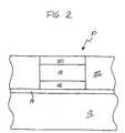
- FIG. 2is an illustration of a cross-section of a memory cell in accordance with an exemplary embodiment of the invention
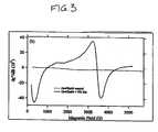
- FIG. 3is a graph showing the low field signal where zero field splitting may be observed in an exemplary embodiment of the invention
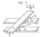
- FIG. 4is a representative portion of a memory array incorporating memory cells in accordance with the invention.
- FIG. 5is a representation of a processor system employing a memory device incorporating exemplary embodiments of memory cells in accordance with the invention.
- waferand “substrate” are to be understood as interchangeable and as including any foundation suitable for supporting a memory element of the invention.
- the substratecan be silicon, silicon-on-insulator (SOI), silicon-on-sapphire (SOS), doped and undoped semiconductors, epitaxial layers of silicon supported by a base semiconductor foundation, and other semiconductor, conductor, or insulator structures.
- SOIsilicon-on-insulator
- SOSsilicon-on-sapphire
- doped and undoped semiconductorsepitaxial layers of silicon supported by a base semiconductor foundation, and other semiconductor, conductor, or insulator structures.
- previous process stepsmay have been utilized to form regions, junctions or material layers in or on the base structure or foundation.
- the semiconductor substrateneed not be silicon-based, but could be based on silicon-germanium, germanium, gallium arsenide, or other known semiconductor materials. Further, the substrate need not be semiconductor-based at all, but can be any material suitable for supporting an integrated circuit memory structure, for instance, polymer, glass, metals, insulated metals, ceramics, and other materials.
- the inventionutilizes zero field splitting (ZFS) properties of certain metal ions to form a memory cell.
- Transition metal ionssuch as ions of Co, Cr, Fe, Mn, Ti, Cu, Zn, V, Cd, and Ni, and others, are preferred and can be added to a host material, such as an organic molecular matrix or an inorganic matrix.
- the selection of the metal ions and the host materialdetermines the zero field splitting energy; the host material may or may not play a role in the zero field splitting properties of the ions in memory operation.
- the selection of these ions and host materialsshould result in microwave absorption energies of about 0.03 cm ⁇ 1 to 3.3 cm ⁇ 1 at zero field to satisfy requirements for memory state sensing.
- the separation of spin states in the metal ions within the host material at zero magnetic fieldshould be be small enough to be able to utilize the energy available on a standard semiconductor chip.
- the host materialif organic, can be polymer based or porphyrin based. If the host material is inorganic, it may be a chalcogenide glass, e.g., arsenic selenide or germanium selenide, a semiconductor, or a silicate, for example.
- FIG. 2shows a simplified illustration of a specific memory cell construction in accordance with an exemplary embodiment of the invention.
- the memory cell 10is shown as supported by a substrate 12 , which may be silicon-based, but as indicated above, the substrate can be any of a number of materials.
- the substrate 12can be formed or provided as is known in the art by conventional means, depending on its composition.
- the optional insulating layer 14is provided over the substrate 12 if it is semiconductor-based.
- the optional insulating layer 14can be, for example, silicon oxide or silicon nitride, and can be formed by CVD (chemical vapor deposition), sputtering, oxidation of the substrate 12 , or other known techniques.
- an electrode 16 of a conductive materialOver the optional insulating layer 14 , or substrate 12 if that layer 14 is excluded, is provided an electrode 16 of a conductive material.
- the conductive material for the electrode 16can be any of a number of materials, including, but not limited to, tungsten, tungsten nitride, aluminum, copper, doped polysilicon, nickel, titanium, and platinum.
- the electrode 16 materialcan be deposited by CVD, PECVD (plasma enhanced chemical vapor deposition), sputtering, plating, or other known techniques, and the electrode 16 can thereafter be defined by patterning and etching, if desired.
- the host material 18can be an organic or inorganic molecular matrix (as indicated above) and can be formed by blanket deposition techniques, which may be followed by patterning and etching if desired, or, alternatively, may be formed by an in-via process; either deposition process may include CVD, sputtering, co-sputtering, thermal evaporation, or other known techniques.
- the host material 18can be about 100 ⁇ to about 2,000 ⁇ thick.
- one suitable and exemplary host material 18is a Ge x Se 100-x glass, for example, a Ge 40 Se 60 glass.
- the glass and ionse.g., Mn +2 ions, which may be provided as MnSe
- the glass and ionsare deposited together by cosputtering or co-evaporation.
- the glassis first deposited, for example, by sputtering, and then a layer of ions is formed over the Ge 40 Se 60 host material 18 , for example, by sputtering or thermal evaporation.
- the ionscan be incorporated into the host material 18 by photodoping or thermal diffusion, or by other means. If the host material 18 itself exhibits zero field splitting properties, the step of adding ions may be omitted.
- the host material 18can incorporate from less than about 0.3% to up to about 10% (by weight) metal ions.
- About 1 wt. % ion concentrationis preferred.
- a second electrode 20is next deposited over the ion-doped host material 18 .
- the second electrode 20can be of the same or similar materials as the first electrode 16 and can be formed by the same or similar techniques.
- the memory device 10 stackcan be surrounded by an insulating material 22 , such as BPSG (borophosphosilicate glass) or polyimide, and the wafer can be planarized by CMP (chemical mechanical polishing) using the top electrode 20 as a stop, if desired.
- the memory device 10 shown in FIG. 2is representative of one of a plurality of such devices that can be arranged in a memory array.
- the Mn +2 ions in the above-described exemplary Ge 40 Se 60 glassenable the host material 18 to display a relatively large microwave absorption at zero field, which enables the device to store data as energy absorption states.
- a memory device in accordance with this exemplary embodimentcan absorb about 0.33 cm ⁇ 1 of energy of a potential pulse having a rise time of about 35 picoseconds and a frequency of about 9.68 GHz. As shown by the graph in FIG. 3 , the zero field splitting absorption is observed at relatively low field signal in the structure of this embodiment.
- the germanium selenide stoichiometryplays a role in the functioning of this exemplary cell, with the Ge 40 Se 60 glass being preferred over other germanium selenide stoichiometries. Other glass types and stoichiometries can be used in the invention, however.
- the first electrode 16can comprise manganese.
- the second electrode 20can be tungsten.
- These electrodes 16 and 20are not limited to such materials, however.
- Other conductive materialssuch as doped polysilicon, titanium, aluminum, copper, silver, platinum, nickel, and conductive nitrides can be used as well.
- metal ions and host materials 18can also be used for a memory device in accordance with the invention. As previously indicated, such combinations should be able to absorb a detectable amount of energy when in a programmed state.
- a standard float glass doped with less than about 1% Mn +2 , Mn +3 , or Fe +3has been shown to absorb a detectable amount of energy in the microwave frequency range.
- Float glasscan comprise Na 2 O-CaO-MgO-SiO 2 , and the metal ions can be incorporated into the glass as about 1 wt. % MnO 2 or Fe 2 O 3 .
- the energy absorption characteristics of these alternative host material/metal ion combinations at zero magnetic fieldhave been known in the art, but never utilized as part of a memory device.
- Other examples of materials that could be engineered to contain transition metals that could be oxidized/reduced by applied potentials or light to exhibit zero field splitting memory behaviorinclude porphyrins, ferrocenes, and perovskites.
- the memory cells 10 of the inventioncan be utilized in a memory array by being formed between conductive intersecting column lines 30 and row lines 32 .
- the host material 18comprising metal ions.
- the host material 18is of the appropriate composition (e.g., the correct matrix material supporting the correct ions and ligands), it can be written, read, and erased in a non-volatile manner for operation as a memory device as discussed herein.
- a memory cell in accordance with an exemplary embodiment of the inventionstores information as a stable energy absorption state; which is one of two states, the other being a stable non-energy-absorbing state.
- the energy absorbing property of the memory cellshould be sufficient to absorb a detectable amount of an energy (e.g., electrical or optical) impulse at a bandwidth corresponding to the splitting at zero field of the ions in the host material.
- Energy, bandwidth frequency, and pulse rise timeare interrelated variables relating to the programming of the memory cell.
- the two memory states of the memory cells of the inventionhave been described as an energy-absorbing state and a non-energy-absorbing state, the invention is not limited to such states. Two energy-absorbing states may also be used, where the amount of energy absorption each state exhibits is great enough for individual detection and also allows effective differentiation between the two states.
- Writing (as well as erasing) the memory cellscan be accomplished by three phenomena: (1) changing the oxidation state of the metal ions of the cell; (2) changing the ligand field environment of the metal ions; each induced either by using a voltage potential or light impulse; or (3) a combination of (1) and (2). Either of these inducement techniques can change the zero field splitting parameters of the metal ions in a host material 18 .
- the exemplary memory device of the inventioncan be written by a potential pulse as already discussed.
- a column line 30is charged with a programming potential while an intersecting row line 32 a is grounded.
- the memory cell 10 a at the intersection of the column line 30 and row line 32 ais then programmed (e.g., by redox reaction or ligand field change) to the stable energy-absorbing memory state from a stable non-energy-absorbing state.
- the specific mechanism enabling the memory cell to switch between energy-absorbing and non-energy-absorbing stateswill vary depending upon the way the metal ion is altered. Examples include a change in oxidation state of the ions (e.g., Mn +2 ) within the host material (e.g., Ge 40 Se 60 ) or because of an alteration of the distribution of molecular species within the memory element of the device such that the metal ions are associated with a charged ligand field environment around the ion. Under the oxidation theory, the metal ions of the host material may form a redox pair, such as Mn +2 /Mn +3 , Cu +2 /Cu +1 , or Fe +2 /Fe +3 , which permits energy absorption within the cell.
- the ligand field around the metal ionsmay undergo a structural change within the memory cell. For example, if a potential applied in a specific direction across the cell causes a rearrangement in the molecular matrix or if the metal ions redistribute non-homogeneously and see more spin-spin interactions (electrons interacting with each other) due to ion proximity, energy absorption can be enabled or disabled within the cell.
- the memory cellcan be non-volatile, or at least has very low volatility compared with prior art memory technologies such as DRAM.
- the programming mechanismis based on a redox reaction, once the potential applied across the cell generates a larger distribution of one redox state of the metal ions, removal of the potential does not initiate a reverse redox reaction. Likewise, a rearrangement of the molecular matrix remains until another input of energy changes the matrix.
- the memory deviceAfter programming, the memory device can be returned to its original energy absorption state.
- One method of turning off programmed devicesis by applying a reverse voltage potential relative to the programming potential of the stimulation pulse.
- Another methodis by utilizing a light pulse.
- the programmed state of the memory cellcan be read, preferably, by sensing the absorption or transmission of energy from a read electrical pulse applied to the cell.
- the metal ions of the cellAfter programming a cell to an energy-absorbing state, the metal ions of the cell have a zero field interaction, which results in the metal ions being able to absorb a detectable amount of energy corresponding to the splitting at zero field.
- the pulse rise timecorresponds to the separation in energy of the electron spin levels at zero field, the signal (or at least a detectable portion thereof) is absorbed by the memory cell and a reduced or absent energy transmission can be sensed by read circuitry.
- the energy applied to the cellremains largely intact and can be sensed by read circuitry as corresponding to the non-programmed state of the cell.
- the energy pulse rise time of the read signalis selected (in accordance with Equations (1 a ) and (1 b )) so that a non-programmed cell does not affect the pulse, but a programmed cell absorbs at least a detectable amount of the transmitted energy.
- Pulse rise timesare specific to the zero field splitting parameters of the molecular system. Pulse rise times in accordance with the exemplary embodiments of the invention ( FIG. 2 ) described above should be about 380 picoseconds to less than 4 picoseconds in order to correspond to the separation in electron spin level energy at zero field of the metal ions used in the memory cells; Mn +2 , Cu +2 , and Fe +2 being examples.
- the memory device's access speedis limited only by the speed of the access electronics.
- a memory cell 10 acan be addressed for reading by a read pulse input at the column line 30 (with row line 32 a grounded). As the pulse propagates down the column line it is absorbed by the memory cell 10 a host material 18 if: (1) the host material 18 is in a zero field splitting state; and (2) the row line 32 a at the address is grounded.
- the memory cell 10 ais read by sense circuitry 34 in electrical communication with the column line 30 according to the amount of the column line 30 pulse absorbed by the memory cell 10 a.
- the memory cells 10can be induced to change state by a light pulse.
- the light pulsemay either make the cells permanently change state (e.g., to an energy-absorbing state) for a write-once device, or a second wavelength of light (or some other energy input) could reverse the state written by the first wavelength (e.g., to a non-energy-absorbing state), making for a non-volatile memory (e.g., random access memory).
- the light pulsecan induce an oxidation state change in the memory cells 10 . Physical changes in the glass matrix host material 18 system or molecular conformal changes may occur.
- the host material 18incorporates multiple transition metal ion species (more than one ion type) to make a memory cell 10 having a multi-state zero field splitting resonance memory, which is capable of storing multiple bits.
- the basic structure of such a memory cell 10can be like that shown in FIG. 2 and described above.
- the host material 18 of this embodimentincorporates at least two metal ion species, for example, one ion can be Mn +2 and another can be Cu +2 . Both can be incorporated in a Ge 40 Se 60 host material.
- This embodimentis capable of multiple oxidation states or multiple configurations which have different zero field splitting parameters. Because each transition metal ion (e.g., ions of Mn, Ti, Co, Cr, Cu, Zn, Ni, Fe, Cd, V, and others) has a different zero field splitting energy in the matrix, each programmed state relating to the different ion types can be accessed for a reading operation using a different electrical energy pulse with a rise time corresponding to the energy splitting of a particular ion.
- transition metal ione.g., ions of Mn, Ti, Co, Cr, Cu, Zn, Ni, Fe, Cd, V, and others
- a pulse corresponding to a zero field splitting energy of 0.35 cm ⁇ 1may be used to read a bit corresponding to Mn +3 ions, but a pulse of greater or lesser magnitude and different rise time may be used for reading a bit stored by Cu +2 , where the latter pulse would have no effect on the bit stored by the Mn +3 ion because rise times are coordinated with the different ion species.
- a single memory cell 10can therefore contain a plurality of independent memory states, which can each be independently read by changing the rise time of the read pulse.
- the memory cells 10 of this embodimentcan be programmed by either application of a light pulse of a certain wavelength or by application of a potential across the memory cell 10 .
- the ions of different metal speciesmay respond to a programming input with either an oxidation state change or a ligand field rearrangement, as discussed.
- FIG. 5shows a typical processor-based system 400 , which includes a memory circuit 448 , for example, a programmable RAM, employing memory devices having memory cells 10 constructed in accordance with the invention.
- a processor systemsuch as computer system, generally comprises a central processing unit (CPU) 444 , such as a microprocessor, a digital signal processor, or other programmable digital logic devices. Such devices communicate with an input/output (I/O) device 446 over a bus 452 .
- the memory 448communicates with the system over the bus 452 , typically by a memory controller.
- the processormay include peripheral devices, such as a disk drive 454 and a CDROM drive 456 , which also communicate with the CPU 444 over the bus 452 .
- Memory 448is preferably constructed as an integrated circuit, which includes one or more memory devices having memory cells 10 . If desired, the memory 448 may be combined with the processor, for example CPU 444 , in a single integrated circuit.
Landscapes
- Engineering & Computer Science (AREA)
- Manufacturing & Machinery (AREA)
- Computer Hardware Design (AREA)
- Semiconductor Memories (AREA)
Abstract
Description
- The invention disclosed in this application is related to the invention disclosed by U.S. patent application ______ (Attorney Docket No. M4065.1009/P1009), filed concurrently with this application by Kristy A. Campbell and Terry L. Gilton. The entirety of this related application is hereby incorporated by reference herein in its entirety.
- The invention relates to memory devices utilizing zero field splitting parameters and methods of making and using such memory devices.
- Integrated circuit designers have always sought the ideal semiconductor memory: a device that is randomly accessible, can be written or read very quickly, is non-volatile, but indefinitely alterable, consumes little power, and is scalable. The search for such devices has led to investigations into atomic-level properties of materials for switching and memory applications.
- Studies have been conducted into electron spin transistors and memory components. Even in the absence of a magnetic field, some metal ions exhibit splitting of the electron spin energy levels. This is referred to as zero field splitting. Zero field splitting is different from Zeeman splitting (i.e., separation of the electron spin energy levels in the presence of an externally applied magnetic field). The difference being that some molecules may exhibit splitting of the electron energy levels at zero externally applied magnetic field, due in part, to the natural crystal fields present around a metal ion (in the case of molecules with transition metal ions) or to spin-spin coupling within a molecule or between molecules. Molecules with transition metals (e.g., Mn, V, Fe, Co, Cr, Ni, Cu, Zn, Cd, and others) are quite frequently paramagnetic and may have electron spin energy levels at zero magnetic field with an energy splitting between levels for which a spin transition is allowed that is within a range detectable with microwave radiation. For example, as shown in
FIG. 1 , Mn+3ions have a spin system with an effective spin S=2, with a positive zero field splitting value. The inset portion ofFIG. 1 is an expanded view of the Ms=±2 energy levels in the region of observed parallel mode electron paramagnetic resonance transitions (indicated by the double arrows). Analytical techniques, such as microwave spectroscopy or electron paramagnetic resonance (EPR) spectroscopy can identify molecular systems that exhibit zero field splitting properties. - Spin-spin interactions occur when there is at least one unpaired electron interacting with another unpaired electron (S greater than or equal to 1, where S is the effective spin). An example molecular system that could give rise to this situation includes a molecule containing Mn+3, which has a total spin S=2 (e.g., the molecule Mn(salen)). In this case, there are 4 unpaired electrons interacting with each other.
- Microwave absorption spectroscopy has been used to identify atomic properties of chemical species. Microwave absorption has been shown to be a viable means of determining energy absorption at frequencies corresponding to the zero field splitting value of the absorbing material.
- It would be advantageous to utilize the zero field splitting properties of ions as a memory device. It would be additionally advantageous if such a memory device was non-volatile or semi-volatile, operated at speeds necessary for present memory functions, and could be scaled to sub-micron sizes.
- An exemplary embodiment of the invention provides a low-volatility or non-volatile memory cell utilizing the zero field splitting properties of a material to store data. The memory cell may incorporate at least one transition metal ion species. In response to an energy pulse, e.g., electrical or optical, the host material can switch between energy absorbing and non-energy absorbing (or less energy absorbing) states based on the zero field splitting properties of the material induced by the applied signal. Exemplary host material and metal ion combinations include chalcogenide glass with manganese ions, standard float glass (e.g., Na2O-CaO-MgO-SiO2) with ions (e.g., Mn ions), perovskite (e.g., CaTiO3and MgSiO3) materials with manganese ions, porphyrins with manganese or zinc, or ferrocenes with ion species.
- Another exemplary embodiment of the invention provides a memory cell, which can store multiple bits of data using a plurality of metal ion species in a single host material.
- These and other features of exemplary embodiments of the invention will be more apparent from the following detailed description and drawings which illustrate the various embodiments.
FIG. 1 is an energy level diagram of an S=2 system illustrating zero field splitting for a transition metal ion species.FIG. 2 is an illustration of a cross-section of a memory cell in accordance with an exemplary embodiment of the invention;FIG. 3 is a graph showing the low field signal where zero field splitting may be observed in an exemplary embodiment of the invention;FIG. 4 is a representative portion of a memory array incorporating memory cells in accordance with the invention; andFIG. 5 is a representation of a processor system employing a memory device incorporating exemplary embodiments of memory cells in accordance with the invention.- In the following detailed description, reference is made to the accompanying drawings, which are a part of the specification, and in which is shown by way of illustration various embodiments whereby the invention may be practiced. These embodiments are described in sufficient detail to enable those skilled in the art to make and use the invention. It is to be understood that other embodiments may be utilized, and that structural, logical, and electrical changes, as well as changes in the materials used, may be made without departing from the spirit and scope of the present invention. Additionally, certain processing steps are described and a particular order of processing steps is disclosed; however, the sequence of steps is not limited to that set forth herein and may be changed as is known in the art, with the exception of steps or acts necessarily occurring in a certain order.
- The terms “wafer” and “substrate” are to be understood as interchangeable and as including any foundation suitable for supporting a memory element of the invention. For example, the substrate can be silicon, silicon-on-insulator (SOI), silicon-on-sapphire (SOS), doped and undoped semiconductors, epitaxial layers of silicon supported by a base semiconductor foundation, and other semiconductor, conductor, or insulator structures. Furthermore, when reference is made to a “wafer” or “substrate” in the following description, previous process steps may have been utilized to form regions, junctions or material layers in or on the base structure or foundation. In addition, the semiconductor substrate need not be silicon-based, but could be based on silicon-germanium, germanium, gallium arsenide, or other known semiconductor materials. Further, the substrate need not be semiconductor-based at all, but can be any material suitable for supporting an integrated circuit memory structure, for instance, polymer, glass, metals, insulated metals, ceramics, and other materials.
- The invention utilizes zero field splitting (ZFS) properties of certain metal ions to form a memory cell. Transition metal ions, such as ions of Co, Cr, Fe, Mn, Ti, Cu, Zn, V, Cd, and Ni, and others, are preferred and can be added to a host material, such as an organic molecular matrix or an inorganic matrix. The selection of the metal ions and the host material determines the zero field splitting energy; the host material may or may not play a role in the zero field splitting properties of the ions in memory operation. The selection of these ions and host materials should result in microwave absorption energies of about 0.03 cm−1to 3.3 cm−1at zero field to satisfy requirements for memory state sensing.
- The separation of spin states in the metal ions within the host material at zero magnetic field should be be small enough to be able to utilize the energy available on a standard semiconductor chip. The host material, if organic, can be polymer based or porphyrin based. If the host material is inorganic, it may be a chalcogenide glass, e.g., arsenic selenide or germanium selenide, a semiconductor, or a silicate, for example.
- Now referring to the figures, where like reference numbers designate like elements,
FIG. 2 shows a simplified illustration of a specific memory cell construction in accordance with an exemplary embodiment of the invention. Thememory cell 10 is shown as supported by asubstrate 12, which may be silicon-based, but as indicated above, the substrate can be any of a number of materials. Thesubstrate 12 can be formed or provided as is known in the art by conventional means, depending on its composition. - An
optional insulating layer 14 is provided over thesubstrate 12 if it is semiconductor-based. Theoptional insulating layer 14 can be, for example, silicon oxide or silicon nitride, and can be formed by CVD (chemical vapor deposition), sputtering, oxidation of thesubstrate 12, or other known techniques. - Over the
optional insulating layer 14, orsubstrate 12 if thatlayer 14 is excluded, is provided anelectrode 16 of a conductive material. The conductive material for theelectrode 16 can be any of a number of materials, including, but not limited to, tungsten, tungsten nitride, aluminum, copper, doped polysilicon, nickel, titanium, and platinum. Theelectrode 16 material can be deposited by CVD, PECVD (plasma enhanced chemical vapor deposition), sputtering, plating, or other known techniques, and theelectrode 16 can thereafter be defined by patterning and etching, if desired. - Over and electrically coupled to the
electrode 18 is deposited a layer ofhost material 18, which incorporates metal ions, such as Mn+2, for example. Thehost material 18 can be an organic or inorganic molecular matrix (as indicated above) and can be formed by blanket deposition techniques, which may be followed by patterning and etching if desired, or, alternatively, may be formed by an in-via process; either deposition process may include CVD, sputtering, co-sputtering, thermal evaporation, or other known techniques. Thehost material 18 can be about 100 Å to about 2,000 Å thick. - For example, one suitable and
exemplary host material 18 is a GexSe100-xglass, for example, a Ge40Se60glass. Preferably, the glass and ions (e.g., Mn+2ions, which may be provided as MnSe) are deposited together by cosputtering or co-evaporation. In another method, the glass is first deposited, for example, by sputtering, and then a layer of ions is formed over the Ge40Se60host material18, for example, by sputtering or thermal evaporation. The ions can be incorporated into thehost material 18 by photodoping or thermal diffusion, or by other means. If thehost material 18 itself exhibits zero field splitting properties, the step of adding ions may be omitted. - Depending on the selection of
host material 18 and metal ion pairing, thehost material 18 can incorporate from less than about 0.3% to up to about 10% (by weight) metal ions. About 1 wt. % ion concentration is preferred. - A
second electrode 20 is next deposited over the ion-dopedhost material 18. Thesecond electrode 20 can be of the same or similar materials as thefirst electrode 16 and can be formed by the same or similar techniques. Thememory device 10 stack can be surrounded by an insulating material22, such as BPSG (borophosphosilicate glass) or polyimide, and the wafer can be planarized by CMP (chemical mechanical polishing) using thetop electrode 20 as a stop, if desired. Thememory device 10 shown inFIG. 2 is representative of one of a plurality of such devices that can be arranged in a memory array. - The Mn+2ions in the above-described exemplary Ge40Se60glass enable the
host material 18 to display a relatively large microwave absorption at zero field, which enables the device to store data as energy absorption states. A memory device in accordance with this exemplary embodiment can absorb about 0.33 cm−1of energy of a potential pulse having a rise time of about 35 picoseconds and a frequency of about 9.68 GHz. As shown by the graph inFIG. 3 , the zero field splitting absorption is observed at relatively low field signal in the structure of this embodiment. The germanium selenide stoichiometry plays a role in the functioning of this exemplary cell, with the Ge40Se60glass being preferred over other germanium selenide stoichiometries. Other glass types and stoichiometries can be used in the invention, however. - In the embodiment discussed in the preceding paragraphs in relation to
FIG. 2 , thefirst electrode 16 can comprise manganese. Thesecond electrode 20 can be tungsten. Theseelectrodes - Other combinations of metal ions and
host materials 18 can also be used for a memory device in accordance with the invention. As previously indicated, such combinations should be able to absorb a detectable amount of energy when in a programmed state. For example, a standard float glass doped with less than about 1% Mn+2, Mn+3, or Fe+3has been shown to absorb a detectable amount of energy in the microwave frequency range. Float glass can comprise Na2O-CaO-MgO-SiO2, and the metal ions can be incorporated into the glass as about 1 wt. % MnO2or Fe2O3. Additionally, borosilicate glasses doped with Cu, Ni, Co, and Fe in high concentrations (greater than about 10%) exhibit detectable non-resonant microwave absorption at zero field. The energy absorption characteristics of these alternative host material/metal ion combinations at zero magnetic field have been known in the art, but never utilized as part of a memory device. Other examples of materials that could be engineered to contain transition metals that could be oxidized/reduced by applied potentials or light to exhibit zero field splitting memory behavior include porphyrins, ferrocenes, and perovskites. - As shown in
FIG. 4 , thememory cells 10 of the invention can be utilized in a memory array by being formed between conductive intersecting column lines30 and row lines32. At each intersection is located thehost material 18 comprising metal ions. When thehost material 18 is of the appropriate composition (e.g., the correct matrix material supporting the correct ions and ligands), it can be written, read, and erased in a non-volatile manner for operation as a memory device as discussed herein. - A memory cell in accordance with an exemplary embodiment of the invention stores information as a stable energy absorption state; which is one of two states, the other being a stable non-energy-absorbing state. The energy absorbing property of the memory cell should be sufficient to absorb a detectable amount of an energy (e.g., electrical or optical) impulse at a bandwidth corresponding to the splitting at zero field of the ions in the host material. Energy, bandwidth frequency, and pulse rise time are interrelated variables relating to the programming of the memory cell. These variables are interrelated in general accordance with the following formulas:
- Although the two memory states of the memory cells of the invention have been described as an energy-absorbing state and a non-energy-absorbing state, the invention is not limited to such states. Two energy-absorbing states may also be used, where the amount of energy absorption each state exhibits is great enough for individual detection and also allows effective differentiation between the two states.
- Writing (as well as erasing) the memory cells can be accomplished by three phenomena: (1) changing the oxidation state of the metal ions of the cell; (2) changing the ligand field environment of the metal ions; each induced either by using a voltage potential or light impulse; or (3) a combination of (1) and (2). Either of these inducement techniques can change the zero field splitting parameters of the metal ions in a
host material 18. - The exemplary memory device of the invention can be written by a potential pulse as already discussed. For example, as shown in
FIG. 4 , acolumn line 30 is charged with a programming potential while an intersecting row line32ais grounded. The memory cell10aat the intersection of thecolumn line 30 and row line32ais then programmed (e.g., by redox reaction or ligand field change) to the stable energy-absorbing memory state from a stable non-energy-absorbing state. - The specific mechanism enabling the memory cell to switch between energy-absorbing and non-energy-absorbing states will vary depending upon the way the metal ion is altered. Examples include a change in oxidation state of the ions (e.g., Mn+2) within the host material (e.g., Ge40Se60) or because of an alteration of the distribution of molecular species within the memory element of the device such that the metal ions are associated with a charged ligand field environment around the ion. Under the oxidation theory, the metal ions of the host material may form a redox pair, such as Mn+2/Mn+3, Cu+2/Cu+1, or Fe+2/Fe+3, which permits energy absorption within the cell. Under the altered ligand theory, the ligand field around the metal ions may undergo a structural change within the memory cell. For example, if a potential applied in a specific direction across the cell causes a rearrangement in the molecular matrix or if the metal ions redistribute non-homogeneously and see more spin-spin interactions (electrons interacting with each other) due to ion proximity, energy absorption can be enabled or disabled within the cell.
- Because the memory cell's ability to store data is based on a changeable physical property of the cell, the memory cell can be non-volatile, or at least has very low volatility compared with prior art memory technologies such as DRAM. For example, if the programming mechanism is based on a redox reaction, once the potential applied across the cell generates a larger distribution of one redox state of the metal ions, removal of the potential does not initiate a reverse redox reaction. Likewise, a rearrangement of the molecular matrix remains until another input of energy changes the matrix.
- After programming, the memory device can be returned to its original energy absorption state. One method of turning off programmed devices is by applying a reverse voltage potential relative to the programming potential of the stimulation pulse. Another method is by utilizing a light pulse.
- The programmed state of the memory cell can be read, preferably, by sensing the absorption or transmission of energy from a read electrical pulse applied to the cell. After programming a cell to an energy-absorbing state, the metal ions of the cell have a zero field interaction, which results in the metal ions being able to absorb a detectable amount of energy corresponding to the splitting at zero field. If the pulse rise time corresponds to the separation in energy of the electron spin levels at zero field, the signal (or at least a detectable portion thereof) is absorbed by the memory cell and a reduced or absent energy transmission can be sensed by read circuitry. However, if no energy is absorbed because the cell is not programmed to an energy-absorbing state, the energy applied to the cell remains largely intact and can be sensed by read circuitry as corresponding to the non-programmed state of the cell.
- The energy pulse rise time of the read signal is selected (in accordance with Equations (1a) and (1b)) so that a non-programmed cell does not affect the pulse, but a programmed cell absorbs at least a detectable amount of the transmitted energy. Pulse rise times are specific to the zero field splitting parameters of the molecular system. Pulse rise times in accordance with the exemplary embodiments of the invention (
FIG. 2 ) described above should be about 380 picoseconds to less than 4 picoseconds in order to correspond to the separation in electron spin level energy at zero field of the metal ions used in the memory cells; Mn+2, Cu+2, and Fe+2being examples. The memory device's access speed is limited only by the speed of the access electronics. - A memory cell10acan be addressed for reading by a read pulse input at the column line30 (with row line32agrounded). As the pulse propagates down the column line it is absorbed by the memory cell10a
host material 18 if: (1) thehost material 18 is in a zero field splitting state; and (2) the row line32aat the address is grounded. The memory cell10ais read bysense circuitry 34 in electrical communication with thecolumn line 30 according to the amount of thecolumn line 30 pulse absorbed by the memory cell10a. - In accordance with another embodiment of the invention, the
memory cells 10 can be induced to change state by a light pulse. The light pulse may either make the cells permanently change state (e.g., to an energy-absorbing state) for a write-once device, or a second wavelength of light (or some other energy input) could reverse the state written by the first wavelength (e.g., to a non-energy-absorbing state), making for a non-volatile memory (e.g., random access memory). The light pulse can induce an oxidation state change in thememory cells 10. Physical changes in the glassmatrix host material 18 system or molecular conformal changes may occur. - In another embodiment in accordance with the invention, the
host material 18 incorporates multiple transition metal ion species (more than one ion type) to make amemory cell 10 having a multi-state zero field splitting resonance memory, which is capable of storing multiple bits. The basic structure of such amemory cell 10 can be like that shown inFIG. 2 and described above. However, where thehost material 18 of the embodiment described in accordance withFIG. 2 is doped only with one metal ion species, thehost material 18 of this embodiment incorporates at least two metal ion species, for example, one ion can be Mn+2and another can be Cu+2. Both can be incorporated in a Ge40Se60host material. - This embodiment is capable of multiple oxidation states or multiple configurations which have different zero field splitting parameters. Because each transition metal ion (e.g., ions of Mn, Ti, Co, Cr, Cu, Zn, Ni, Fe, Cd, V, and others) has a different zero field splitting energy in the matrix, each programmed state relating to the different ion types can be accessed for a reading operation using a different electrical energy pulse with a rise time corresponding to the energy splitting of a particular ion. For example, a pulse corresponding to a zero field splitting energy of 0.35 cm−1may be used to read a bit corresponding to Mn+3ions, but a pulse of greater or lesser magnitude and different rise time may be used for reading a bit stored by Cu+2, where the latter pulse would have no effect on the bit stored by the Mn+3ion because rise times are coordinated with the different ion species. A
single memory cell 10 can therefore contain a plurality of independent memory states, which can each be independently read by changing the rise time of the read pulse. As with other embodiments discussed above, thememory cells 10 of this embodiment can be programmed by either application of a light pulse of a certain wavelength or by application of a potential across thememory cell 10. The ions of different metal species may respond to a programming input with either an oxidation state change or a ligand field rearrangement, as discussed. - In this embodiment, it is possible that programming for an ion species with a higher potential programming needs could affect the programmed state of an ion species with lower potential programming needs. Therefore, there should be an order in programming through the various ion species types that takes this into consideration. It is also possible to use various combinations of electrical and light pulses to program the memory cells. The reading of memory states would be independent because pulse rise times used for reading the various ions of a memory cell would be specific to individual ion types and would have no effect on other ion types since these rise times can be correlated to the zero field splitting energy.
FIG. 5 shows a typical processor-basedsystem 400, which includes amemory circuit 448, for example, a programmable RAM, employing memory devices havingmemory cells 10 constructed in accordance with the invention. A processor system, such as computer system, generally comprises a central processing unit (CPU)444, such as a microprocessor, a digital signal processor, or other programmable digital logic devices. Such devices communicate with an input/output (I/O)device 446 over abus 452. Thememory 448 communicates with the system over thebus 452, typically by a memory controller.- In the case of a computer system, the processor may include peripheral devices, such as a
disk drive 454 and aCDROM drive 456, which also communicate with theCPU 444 over thebus 452.Memory 448 is preferably constructed as an integrated circuit, which includes one or more memory devices havingmemory cells 10. If desired, thememory 448 may be combined with the processor, forexample CPU 444, in a single integrated circuit. - The processes and devices described above are merely illustrative of but a few of the preferred methods and devices that could be used and produced in accordance with the invention. The above description and drawings illustrate embodiments, which achieve the objects, features, and advantages of the invention. However, it is not intended that the invention be strictly limited to the above-described and illustrated embodiments. Any modifications of the invention that come within the spirit and scope of the following claims should be considered part of the invention.
- What is claimed as new and desired to be protected by Letters Patent of the United States is:
Claims (77)
Priority Applications (1)
| Application Number | Priority Date | Filing Date | Title |
|---|---|---|---|
| US10/765,911US7105864B2 (en) | 2004-01-29 | 2004-01-29 | Non-volatile zero field splitting resonance memory |
Applications Claiming Priority (1)
| Application Number | Priority Date | Filing Date | Title |
|---|---|---|---|
| US10/765,911US7105864B2 (en) | 2004-01-29 | 2004-01-29 | Non-volatile zero field splitting resonance memory |
Publications (2)
| Publication Number | Publication Date |
|---|---|
| US20050167689A1true US20050167689A1 (en) | 2005-08-04 |
| US7105864B2 US7105864B2 (en) | 2006-09-12 |
Family
ID=34807564
Family Applications (1)
| Application Number | Title | Priority Date | Filing Date |
|---|---|---|---|
| US10/765,911Expired - LifetimeUS7105864B2 (en) | 2004-01-29 | 2004-01-29 | Non-volatile zero field splitting resonance memory |
Country Status (1)
| Country | Link |
|---|---|
| US (1) | US7105864B2 (en) |
Cited By (1)
| Publication number | Priority date | Publication date | Assignee | Title |
|---|---|---|---|---|
| US20070045604A1 (en)* | 2005-08-30 | 2007-03-01 | Micron Technology, Inc. | Resistance variable memory device with nanoparticle electrode and method of fabrication |
Families Citing this family (6)
| Publication number | Priority date | Publication date | Assignee | Title |
|---|---|---|---|---|
| US7366030B2 (en)* | 2004-01-29 | 2008-04-29 | Micron Technology, Inc. | Simultaneous read circuit for multiple memory cells |
| WO2008088599A2 (en) | 2006-10-19 | 2008-07-24 | Boise State University | Forced ion migration for chalcogenide phase change memory device |
| US8467236B2 (en) | 2008-08-01 | 2013-06-18 | Boise State University | Continuously variable resistor |
| US8238146B2 (en)* | 2008-08-01 | 2012-08-07 | Boise State University | Variable integrated analog resistor |
| US20110079709A1 (en)* | 2009-10-07 | 2011-04-07 | Campbell Kristy A | Wide band sensor |
| US8284590B2 (en) | 2010-05-06 | 2012-10-09 | Boise State University | Integratable programmable capacitive device |
Citations (88)
| Publication number | Priority date | Publication date | Assignee | Title |
|---|---|---|---|---|
| US3271591A (en)* | 1963-09-20 | 1966-09-06 | Energy Conversion Devices Inc | Symmetrical current controlling device |
| US3961314A (en)* | 1974-03-05 | 1976-06-01 | Energy Conversion Devices, Inc. | Structure and method for producing an image |
| US3966317A (en)* | 1974-04-08 | 1976-06-29 | Energy Conversion Devices, Inc. | Dry process production of archival microform records from hard copy |
| US3983542A (en)* | 1970-08-13 | 1976-09-28 | Energy Conversion Devices, Inc. | Method and apparatus for recording information |
| US4267261A (en)* | 1971-07-15 | 1981-05-12 | Energy Conversion Devices, Inc. | Method for full format imaging |
| US4597162A (en)* | 1983-01-18 | 1986-07-01 | Energy Conversion Devices, Inc. | Method for making, parallel preprogramming or field programming of electronic matrix arrays |
| US4608296A (en)* | 1983-12-06 | 1986-08-26 | Energy Conversion Devices, Inc. | Superconducting films and devices exhibiting AC to DC conversion |
| US4637895A (en)* | 1985-04-01 | 1987-01-20 | Energy Conversion Devices, Inc. | Gas mixtures for the vapor deposition of semiconductor material |
| US4646266A (en)* | 1984-09-28 | 1987-02-24 | Energy Conversion Devices, Inc. | Programmable semiconductor structures and methods for using the same |
| US4664939A (en)* | 1985-04-01 | 1987-05-12 | Energy Conversion Devices, Inc. | Vertical semiconductor processor |
| US4668968A (en)* | 1984-05-14 | 1987-05-26 | Energy Conversion Devices, Inc. | Integrated circuit compatible thin film field effect transistor and method of making same |
| US4670763A (en)* | 1984-05-14 | 1987-06-02 | Energy Conversion Devices, Inc. | Thin film field effect transistor |
| US4673957A (en)* | 1984-05-14 | 1987-06-16 | Energy Conversion Devices, Inc. | Integrated circuit compatible thin film field effect transistor and method of making same |
| US4678679A (en)* | 1984-06-25 | 1987-07-07 | Energy Conversion Devices, Inc. | Continuous deposition of activated process gases |
| US4728406A (en)* | 1986-08-18 | 1988-03-01 | Energy Conversion Devices, Inc. | Method for plasma - coating a semiconductor body |
| US4737379A (en)* | 1982-09-24 | 1988-04-12 | Energy Conversion Devices, Inc. | Plasma deposited coatings, and low temperature plasma method of making same |
| US4766471A (en)* | 1986-01-23 | 1988-08-23 | Energy Conversion Devices, Inc. | Thin film electro-optical devices |
| US4769338A (en)* | 1984-05-14 | 1988-09-06 | Energy Conversion Devices, Inc. | Thin film field effect transistor and method of making same |
| US4775425A (en)* | 1987-07-27 | 1988-10-04 | Energy Conversion Devices, Inc. | P and n-type microcrystalline semiconductor alloy material including band gap widening elements, devices utilizing same |
| US4809044A (en)* | 1986-08-22 | 1989-02-28 | Energy Conversion Devices, Inc. | Thin film overvoltage protection devices |
| US4818717A (en)* | 1986-06-27 | 1989-04-04 | Energy Conversion Devices, Inc. | Method for making electronic matrix arrays |
| US4843443A (en)* | 1984-05-14 | 1989-06-27 | Energy Conversion Devices, Inc. | Thin film field effect transistor and method of making same |
| US4845533A (en)* | 1986-08-22 | 1989-07-04 | Energy Conversion Devices, Inc. | Thin film electrical devices with amorphous carbon electrodes and method of making same |
| US4853785A (en)* | 1986-10-15 | 1989-08-01 | Energy Conversion Devices, Inc. | Electronic camera including electronic signal storage cartridge |
| US4891330A (en)* | 1987-07-27 | 1990-01-02 | Energy Conversion Devices, Inc. | Method of fabricating n-type and p-type microcrystalline semiconductor alloy material including band gap widening elements |
| US5128099A (en)* | 1991-02-15 | 1992-07-07 | Energy Conversion Devices, Inc. | Congruent state changeable optical memory material and device |
| US5159661A (en)* | 1990-10-05 | 1992-10-27 | Energy Conversion Devices, Inc. | Vertically interconnected parallel distributed processor |
| US5177567A (en)* | 1991-07-19 | 1993-01-05 | Energy Conversion Devices, Inc. | Thin-film structure for chalcogenide electrical switching devices and process therefor |
| US5296716A (en)* | 1991-01-18 | 1994-03-22 | Energy Conversion Devices, Inc. | Electrically erasable, directly overwritable, multibit single cell memory elements and arrays fabricated therefrom |
| US5335219A (en)* | 1991-01-18 | 1994-08-02 | Ovshinsky Stanford R | Homogeneous composition of microcrystalline semiconductor material, semiconductor devices and directly overwritable memory elements fabricated therefrom, and arrays fabricated from the memory elements |
| US5341328A (en)* | 1991-01-18 | 1994-08-23 | Energy Conversion Devices, Inc. | Electrically erasable memory elements having reduced switching current requirements and increased write/erase cycle life |
| US5359205A (en)* | 1991-11-07 | 1994-10-25 | Energy Conversion Devices, Inc. | Electrically erasable memory elements characterized by reduced current and improved thermal stability |
| US5406509A (en)* | 1991-01-18 | 1995-04-11 | Energy Conversion Devices, Inc. | Electrically erasable, directly overwritable, multibit single cell memory elements and arrays fabricated therefrom |
| US5414271A (en)* | 1991-01-18 | 1995-05-09 | Energy Conversion Devices, Inc. | Electrically erasable memory elements having improved set resistance stability |
| US5530263A (en)* | 1994-08-16 | 1996-06-25 | International Business Machines Corporation | Three dot computing elements |
| US5534711A (en)* | 1991-01-18 | 1996-07-09 | Energy Conversion Devices, Inc. | Electrically erasable, directly overwritable, multibit single cell memory elements and arrays fabricated therefrom |
| US5534712A (en)* | 1991-01-18 | 1996-07-09 | Energy Conversion Devices, Inc. | Electrically erasable memory elements characterized by reduced current and improved thermal stability |
| US5536947A (en)* | 1991-01-18 | 1996-07-16 | Energy Conversion Devices, Inc. | Electrically erasable, directly overwritable, multibit single cell memory element and arrays fabricated therefrom |
| US5543737A (en)* | 1995-02-10 | 1996-08-06 | Energy Conversion Devices, Inc. | Logical operation circuit employing two-terminal chalcogenide switches |
| US5591501A (en)* | 1995-12-20 | 1997-01-07 | Energy Conversion Devices, Inc. | Optical recording medium having a plurality of discrete phase change data recording points |
| US5596522A (en)* | 1991-01-18 | 1997-01-21 | Energy Conversion Devices, Inc. | Homogeneous compositions of microcrystalline semiconductor material, semiconductor devices and directly overwritable memory elements fabricated therefrom, and arrays fabricated from the memory elements |
| US5714768A (en)* | 1995-10-24 | 1998-02-03 | Energy Conversion Devices, Inc. | Second-layer phase change memory array on top of a logic device |
| US5792330A (en)* | 1995-05-31 | 1998-08-11 | Board Of Regents, The University Of Texas System | Lanthanide metal cations for concurrent detection and separation in capillary electrophoresis |
| US5912839A (en)* | 1998-06-23 | 1999-06-15 | Energy Conversion Devices, Inc. | Universal memory element and method of programming same |
| US5933365A (en)* | 1997-06-19 | 1999-08-03 | Energy Conversion Devices, Inc. | Memory element with energy control mechanism |
| US6011757A (en)* | 1998-01-27 | 2000-01-04 | Ovshinsky; Stanford R. | Optical recording media having increased erasability |
| US6052519A (en)* | 1996-12-20 | 2000-04-18 | The University Of Queensland | Computer simulation of magnetic resonance spectra employing homotopy |
| US6061265A (en)* | 1998-12-23 | 2000-05-09 | Intel Corporation | Quantum magnetic memory |
| US6087674A (en)* | 1996-10-28 | 2000-07-11 | Energy Conversion Devices, Inc. | Memory element with memory material comprising phase-change material and dielectric material |
| US6208553B1 (en)* | 1999-07-01 | 2001-03-27 | The Regents Of The University Of California | High density non-volatile memory device incorporating thiol-derivatized porphyrins |
| US6212093B1 (en)* | 2000-01-14 | 2001-04-03 | North Carolina State University | High-density non-volatile memory devices incorporating sandwich coordination compounds |
| US6218718B1 (en)* | 1996-04-26 | 2001-04-17 | Isis Innovation Limited | Spin transistor |
| USRE37259E1 (en)* | 1996-04-19 | 2001-07-03 | Energy Conversion Devices, Inc. | Multibit single cell memory element having tapered contact |
| US6272038B1 (en)* | 2000-01-14 | 2001-08-07 | North Carolina State University | High-density non-volatile memory devices incorporating thiol-derivatized porphyrin trimers |
| US6339544B1 (en)* | 2000-09-29 | 2002-01-15 | Intel Corporation | Method to enhance performance of thermal resistor device |
| US6381169B1 (en)* | 1999-07-01 | 2002-04-30 | The Regents Of The University Of California | High density non-volatile memory device |
| US6404665B1 (en)* | 2000-09-29 | 2002-06-11 | Intel Corporation | Compositionally modified resistive electrode |
| US6429064B1 (en)* | 2000-09-29 | 2002-08-06 | Intel Corporation | Reduced contact area of sidewall conductor |
| US6437383B1 (en)* | 2000-12-21 | 2002-08-20 | Intel Corporation | Dual trench isolation for a phase-change memory cell and method of making same |
| US6507061B1 (en)* | 2001-08-31 | 2003-01-14 | Intel Corporation | Multiple layer phase-change memory |
| US6511862B2 (en)* | 2001-06-30 | 2003-01-28 | Ovonyx, Inc. | Modified contact for programmable devices |
| US6512241B1 (en)* | 2001-12-31 | 2003-01-28 | Intel Corporation | Phase change material memory device |
| US6511867B2 (en)* | 2001-06-30 | 2003-01-28 | Ovonyx, Inc. | Utilizing atomic layer deposition for programmable device |
| US6514805B2 (en)* | 2001-06-30 | 2003-02-04 | Intel Corporation | Trench sidewall profile for device isolation |
| US6531373B2 (en)* | 2000-12-27 | 2003-03-11 | Ovonyx, Inc. | Method of forming a phase-change memory cell using silicon on insulator low electrode in charcogenide elements |
| US20030048744A1 (en)* | 2001-09-01 | 2003-03-13 | Ovshinsky Stanford R. | Increased data storage in optical data storage and retrieval systems using blue lasers and/or plasmon lenses |
| US6534781B2 (en)* | 2000-12-26 | 2003-03-18 | Ovonyx, Inc. | Phase-change memory bipolar array utilizing a single shallow trench isolation for creating an individual active area region for two memory array elements and one bipolar base contact |
| US6545907B1 (en)* | 2001-10-30 | 2003-04-08 | Ovonyx, Inc. | Technique and apparatus for performing write operations to a phase change material memory device |
| US6545287B2 (en)* | 2001-09-07 | 2003-04-08 | Intel Corporation | Using selective deposition to form phase-change memory cells |
| US6555860B2 (en)* | 2000-09-29 | 2003-04-29 | Intel Corporation | Compositionally modified resistive electrode |
| US6563164B2 (en)* | 2000-09-29 | 2003-05-13 | Ovonyx, Inc. | Compositionally modified resistive electrode |
| US6566700B2 (en)* | 2001-10-11 | 2003-05-20 | Ovonyx, Inc. | Carbon-containing interfacial layer for phase-change memory |
| US6567293B1 (en)* | 2000-09-29 | 2003-05-20 | Ovonyx, Inc. | Single level metal memory cell using chalcogenide cladding |
| US6570784B2 (en)* | 2001-06-29 | 2003-05-27 | Ovonyx, Inc. | Programming a phase-change material memory |
| US6569705B2 (en)* | 2000-12-21 | 2003-05-27 | Intel Corporation | Metal structure for a phase-change memory device |
| US6576921B2 (en)* | 2001-11-08 | 2003-06-10 | Intel Corporation | Isolating phase change material memory cells |
| US6586761B2 (en)* | 2001-09-07 | 2003-07-01 | Intel Corporation | Phase change material memory device |
| US6590807B2 (en)* | 2001-08-02 | 2003-07-08 | Intel Corporation | Method for reading a structural phase-change memory |
| US6589714B2 (en)* | 2001-06-26 | 2003-07-08 | Ovonyx, Inc. | Method for making programmable resistance memory element using silylated photoresist |
| US6605527B2 (en)* | 2001-06-30 | 2003-08-12 | Intel Corporation | Reduced area intersection between electrode and programming element |
| US6613604B2 (en)* | 2001-08-02 | 2003-09-02 | Ovonyx, Inc. | Method for making small pore for use in programmable resistance memory element |
| US6625054B2 (en)* | 2001-12-28 | 2003-09-23 | Intel Corporation | Method and apparatus to program a phase change memory |
| US6673700B2 (en)* | 2001-06-30 | 2004-01-06 | Ovonyx, Inc. | Reduced area intersection between electrode and programming element |
| US6687427B2 (en)* | 2000-12-29 | 2004-02-03 | Intel Corporation | Optic switch |
| US6690026B2 (en)* | 2001-09-28 | 2004-02-10 | Intel Corporation | Method of fabricating a three-dimensional array of active media |
| US6696355B2 (en)* | 2000-12-14 | 2004-02-24 | Ovonyx, Inc. | Method to selectively increase the top resistance of the lower programming electrode in a phase-change memory |
| US20040035401A1 (en)* | 2002-08-26 | 2004-02-26 | Subramanian Ramachandran | Hydrogen powered scooter |
| US6714954B2 (en)* | 2002-05-10 | 2004-03-30 | Energy Conversion Devices, Inc. | Methods of factoring and modular arithmetic |
Family Cites Families (18)
| Publication number | Priority date | Publication date | Assignee | Title |
|---|---|---|---|---|
| US4177474A (en) | 1977-05-18 | 1979-12-04 | Energy Conversion Devices, Inc. | High temperature amorphous semiconductor member and method of making the same |
| US4710899A (en) | 1985-06-10 | 1987-12-01 | Energy Conversion Devices, Inc. | Data storage medium incorporating a transition metal for increased switching speed |
| US4788594A (en) | 1986-10-15 | 1988-11-29 | Energy Conversion Devices, Inc. | Solid state electronic camera including thin film matrix of photosensors |
| US5166758A (en) | 1991-01-18 | 1992-11-24 | Energy Conversion Devices, Inc. | Electrically erasable phase change memory |
| US6304481B1 (en) | 1994-01-31 | 2001-10-16 | Terastore, Inc. | Method and apparatus for storing data using spin-polarized electrons |
| US5694054A (en) | 1995-11-28 | 1997-12-02 | Energy Conversion Devices, Inc. | Integrated drivers for flat panel displays employing chalcogenide logic elements |
| US5825046A (en) | 1996-10-28 | 1998-10-20 | Energy Conversion Devices, Inc. | Composite memory material comprising a mixture of phase-change memory material and dielectric material |
| US6141241A (en) | 1998-06-23 | 2000-10-31 | Energy Conversion Devices, Inc. | Universal memory element with systems employing same and apparatus and method for reading, writing and programming same |
| US6324091B1 (en) | 2000-01-14 | 2001-11-27 | The Regents Of The University Of California | Tightly coupled porphyrin macrocycles for molecular memory storage |
| IT1316829B1 (en)* | 2000-03-22 | 2003-05-12 | Consiglio Nazionale Ricerche | PROCEDURE AND DEVICE FOR THE TRANSFER OF CHARGE CARRIERS WITH POLARIZED SPIN |
| US6501111B1 (en) | 2000-06-30 | 2002-12-31 | Intel Corporation | Three-dimensional (3D) programmable device |
| US6649928B2 (en) | 2000-12-13 | 2003-11-18 | Intel Corporation | Method to selectively remove one side of a conductive bottom electrode of a phase-change memory cell and structure obtained thereby |
| US6646297B2 (en) | 2000-12-26 | 2003-11-11 | Ovonyx, Inc. | Lower electrode isolation in a double-wide trench |
| US6480438B1 (en) | 2001-06-12 | 2002-11-12 | Ovonyx, Inc. | Providing equal cell programming conditions across a large and high density array of phase-change memory cells |
| US6487113B1 (en) | 2001-06-29 | 2002-11-26 | Ovonyx, Inc. | Programming a phase-change memory with slow quench time |
| US6462984B1 (en) | 2001-06-29 | 2002-10-08 | Intel Corporation | Biasing scheme of floating unselected wordlines and bitlines of a diode-based memory array |
| US6642102B2 (en) | 2001-06-30 | 2003-11-04 | Intel Corporation | Barrier material encapsulation of programmable material |
| US6667900B2 (en) | 2001-12-28 | 2003-12-23 | Ovonyx, Inc. | Method and apparatus to operate a memory cell |
- 2004
- 2004-01-29USUS10/765,911patent/US7105864B2/ennot_activeExpired - Lifetime
Patent Citations (99)
| Publication number | Priority date | Publication date | Assignee | Title |
|---|---|---|---|---|
| US3271591A (en)* | 1963-09-20 | 1966-09-06 | Energy Conversion Devices Inc | Symmetrical current controlling device |
| US3983542A (en)* | 1970-08-13 | 1976-09-28 | Energy Conversion Devices, Inc. | Method and apparatus for recording information |
| US3988720A (en)* | 1970-08-13 | 1976-10-26 | Energy Conversion Devices, Inc. | Recording and retrieving information in an amorphous memory material using a catalytic material |
| US4267261A (en)* | 1971-07-15 | 1981-05-12 | Energy Conversion Devices, Inc. | Method for full format imaging |
| US3961314A (en)* | 1974-03-05 | 1976-06-01 | Energy Conversion Devices, Inc. | Structure and method for producing an image |
| US3966317A (en)* | 1974-04-08 | 1976-06-29 | Energy Conversion Devices, Inc. | Dry process production of archival microform records from hard copy |
| US4737379A (en)* | 1982-09-24 | 1988-04-12 | Energy Conversion Devices, Inc. | Plasma deposited coatings, and low temperature plasma method of making same |
| US4597162A (en)* | 1983-01-18 | 1986-07-01 | Energy Conversion Devices, Inc. | Method for making, parallel preprogramming or field programming of electronic matrix arrays |
| US4608296A (en)* | 1983-12-06 | 1986-08-26 | Energy Conversion Devices, Inc. | Superconducting films and devices exhibiting AC to DC conversion |
| US4769338A (en)* | 1984-05-14 | 1988-09-06 | Energy Conversion Devices, Inc. | Thin film field effect transistor and method of making same |
| US4843443A (en)* | 1984-05-14 | 1989-06-27 | Energy Conversion Devices, Inc. | Thin film field effect transistor and method of making same |
| US4668968A (en)* | 1984-05-14 | 1987-05-26 | Energy Conversion Devices, Inc. | Integrated circuit compatible thin film field effect transistor and method of making same |
| US4670763A (en)* | 1984-05-14 | 1987-06-02 | Energy Conversion Devices, Inc. | Thin film field effect transistor |
| US4673957A (en)* | 1984-05-14 | 1987-06-16 | Energy Conversion Devices, Inc. | Integrated circuit compatible thin film field effect transistor and method of making same |
| US4678679A (en)* | 1984-06-25 | 1987-07-07 | Energy Conversion Devices, Inc. | Continuous deposition of activated process gases |
| US4646266A (en)* | 1984-09-28 | 1987-02-24 | Energy Conversion Devices, Inc. | Programmable semiconductor structures and methods for using the same |
| US4664939A (en)* | 1985-04-01 | 1987-05-12 | Energy Conversion Devices, Inc. | Vertical semiconductor processor |
| US4698234A (en)* | 1985-04-01 | 1987-10-06 | Energy Conversion Devices, Inc. | Vapor deposition of semiconductor material |
| US4696758A (en)* | 1985-04-01 | 1987-09-29 | Energy Conversion Devices, Inc. | Gas mixtures for the vapor deposition of semiconductor material |
| US4637895A (en)* | 1985-04-01 | 1987-01-20 | Energy Conversion Devices, Inc. | Gas mixtures for the vapor deposition of semiconductor material |
| US4766471A (en)* | 1986-01-23 | 1988-08-23 | Energy Conversion Devices, Inc. | Thin film electro-optical devices |
| US4818717A (en)* | 1986-06-27 | 1989-04-04 | Energy Conversion Devices, Inc. | Method for making electronic matrix arrays |
| US4728406A (en)* | 1986-08-18 | 1988-03-01 | Energy Conversion Devices, Inc. | Method for plasma - coating a semiconductor body |
| US4845533A (en)* | 1986-08-22 | 1989-07-04 | Energy Conversion Devices, Inc. | Thin film electrical devices with amorphous carbon electrodes and method of making same |
| US4809044A (en)* | 1986-08-22 | 1989-02-28 | Energy Conversion Devices, Inc. | Thin film overvoltage protection devices |
| US4853785A (en)* | 1986-10-15 | 1989-08-01 | Energy Conversion Devices, Inc. | Electronic camera including electronic signal storage cartridge |
| US4775425A (en)* | 1987-07-27 | 1988-10-04 | Energy Conversion Devices, Inc. | P and n-type microcrystalline semiconductor alloy material including band gap widening elements, devices utilizing same |
| US4891330A (en)* | 1987-07-27 | 1990-01-02 | Energy Conversion Devices, Inc. | Method of fabricating n-type and p-type microcrystalline semiconductor alloy material including band gap widening elements |
| US5159661A (en)* | 1990-10-05 | 1992-10-27 | Energy Conversion Devices, Inc. | Vertically interconnected parallel distributed processor |
| US5414271A (en)* | 1991-01-18 | 1995-05-09 | Energy Conversion Devices, Inc. | Electrically erasable memory elements having improved set resistance stability |
| US5536947A (en)* | 1991-01-18 | 1996-07-16 | Energy Conversion Devices, Inc. | Electrically erasable, directly overwritable, multibit single cell memory element and arrays fabricated therefrom |
| US5296716A (en)* | 1991-01-18 | 1994-03-22 | Energy Conversion Devices, Inc. | Electrically erasable, directly overwritable, multibit single cell memory elements and arrays fabricated therefrom |
| US5335219A (en)* | 1991-01-18 | 1994-08-02 | Ovshinsky Stanford R | Homogeneous composition of microcrystalline semiconductor material, semiconductor devices and directly overwritable memory elements fabricated therefrom, and arrays fabricated from the memory elements |
| US5341328A (en)* | 1991-01-18 | 1994-08-23 | Energy Conversion Devices, Inc. | Electrically erasable memory elements having reduced switching current requirements and increased write/erase cycle life |
| US5596522A (en)* | 1991-01-18 | 1997-01-21 | Energy Conversion Devices, Inc. | Homogeneous compositions of microcrystalline semiconductor material, semiconductor devices and directly overwritable memory elements fabricated therefrom, and arrays fabricated from the memory elements |
| US5406509A (en)* | 1991-01-18 | 1995-04-11 | Energy Conversion Devices, Inc. | Electrically erasable, directly overwritable, multibit single cell memory elements and arrays fabricated therefrom |
| US5534712A (en)* | 1991-01-18 | 1996-07-09 | Energy Conversion Devices, Inc. | Electrically erasable memory elements characterized by reduced current and improved thermal stability |
| US5534711A (en)* | 1991-01-18 | 1996-07-09 | Energy Conversion Devices, Inc. | Electrically erasable, directly overwritable, multibit single cell memory elements and arrays fabricated therefrom |
| US5128099A (en)* | 1991-02-15 | 1992-07-07 | Energy Conversion Devices, Inc. | Congruent state changeable optical memory material and device |
| US5177567A (en)* | 1991-07-19 | 1993-01-05 | Energy Conversion Devices, Inc. | Thin-film structure for chalcogenide electrical switching devices and process therefor |
| US5359205A (en)* | 1991-11-07 | 1994-10-25 | Energy Conversion Devices, Inc. | Electrically erasable memory elements characterized by reduced current and improved thermal stability |
| US5530263A (en)* | 1994-08-16 | 1996-06-25 | International Business Machines Corporation | Three dot computing elements |
| US5543737A (en)* | 1995-02-10 | 1996-08-06 | Energy Conversion Devices, Inc. | Logical operation circuit employing two-terminal chalcogenide switches |
| US5792330A (en)* | 1995-05-31 | 1998-08-11 | Board Of Regents, The University Of Texas System | Lanthanide metal cations for concurrent detection and separation in capillary electrophoresis |
| US5714768A (en)* | 1995-10-24 | 1998-02-03 | Energy Conversion Devices, Inc. | Second-layer phase change memory array on top of a logic device |
| US5591501A (en)* | 1995-12-20 | 1997-01-07 | Energy Conversion Devices, Inc. | Optical recording medium having a plurality of discrete phase change data recording points |
| USRE37259E1 (en)* | 1996-04-19 | 2001-07-03 | Energy Conversion Devices, Inc. | Multibit single cell memory element having tapered contact |
| US6218718B1 (en)* | 1996-04-26 | 2001-04-17 | Isis Innovation Limited | Spin transistor |
| US6087674A (en)* | 1996-10-28 | 2000-07-11 | Energy Conversion Devices, Inc. | Memory element with memory material comprising phase-change material and dielectric material |
| US6052519A (en)* | 1996-12-20 | 2000-04-18 | The University Of Queensland | Computer simulation of magnetic resonance spectra employing homotopy |
| US5933365A (en)* | 1997-06-19 | 1999-08-03 | Energy Conversion Devices, Inc. | Memory element with energy control mechanism |
| US6011757A (en)* | 1998-01-27 | 2000-01-04 | Ovshinsky; Stanford R. | Optical recording media having increased erasability |
| US5912839A (en)* | 1998-06-23 | 1999-06-15 | Energy Conversion Devices, Inc. | Universal memory element and method of programming same |
| US6061265A (en)* | 1998-12-23 | 2000-05-09 | Intel Corporation | Quantum magnetic memory |
| US6208553B1 (en)* | 1999-07-01 | 2001-03-27 | The Regents Of The University Of California | High density non-volatile memory device incorporating thiol-derivatized porphyrins |
| US6381169B1 (en)* | 1999-07-01 | 2002-04-30 | The Regents Of The University Of California | High density non-volatile memory device |
| US6451942B1 (en)* | 2000-01-14 | 2002-09-17 | North Carolina State University | Substrates carrying polymers of linked sandwich coordination compounds and methods of use thereof |
| US6212093B1 (en)* | 2000-01-14 | 2001-04-03 | North Carolina State University | High-density non-volatile memory devices incorporating sandwich coordination compounds |
| US6272038B1 (en)* | 2000-01-14 | 2001-08-07 | North Carolina State University | High-density non-volatile memory devices incorporating thiol-derivatized porphyrin trimers |
| US6339544B1 (en)* | 2000-09-29 | 2002-01-15 | Intel Corporation | Method to enhance performance of thermal resistor device |
| US6555860B2 (en)* | 2000-09-29 | 2003-04-29 | Intel Corporation | Compositionally modified resistive electrode |
| US6404665B1 (en)* | 2000-09-29 | 2002-06-11 | Intel Corporation | Compositionally modified resistive electrode |
| US6567293B1 (en)* | 2000-09-29 | 2003-05-20 | Ovonyx, Inc. | Single level metal memory cell using chalcogenide cladding |
| US6597009B2 (en)* | 2000-09-29 | 2003-07-22 | Intel Corporation | Reduced contact area of sidewall conductor |
| US6621095B2 (en)* | 2000-09-29 | 2003-09-16 | Ovonyx, Inc. | Method to enhance performance of thermal resistor device |
| US6429064B1 (en)* | 2000-09-29 | 2002-08-06 | Intel Corporation | Reduced contact area of sidewall conductor |
| US6563164B2 (en)* | 2000-09-29 | 2003-05-13 | Ovonyx, Inc. | Compositionally modified resistive electrode |
| US6696355B2 (en)* | 2000-12-14 | 2004-02-24 | Ovonyx, Inc. | Method to selectively increase the top resistance of the lower programming electrode in a phase-change memory |
| US6437383B1 (en)* | 2000-12-21 | 2002-08-20 | Intel Corporation | Dual trench isolation for a phase-change memory cell and method of making same |
| US6569705B2 (en)* | 2000-12-21 | 2003-05-27 | Intel Corporation | Metal structure for a phase-change memory device |
| US6593176B2 (en)* | 2000-12-26 | 2003-07-15 | Ovonyx, Inc. | Method for forming phase-change memory bipolar array utilizing a single shallow trench isolation for creating an individual active area region for two memory array elements and one bipolar base contact |
| US6534781B2 (en)* | 2000-12-26 | 2003-03-18 | Ovonyx, Inc. | Phase-change memory bipolar array utilizing a single shallow trench isolation for creating an individual active area region for two memory array elements and one bipolar base contact |
| US6531373B2 (en)* | 2000-12-27 | 2003-03-11 | Ovonyx, Inc. | Method of forming a phase-change memory cell using silicon on insulator low electrode in charcogenide elements |
| US6687427B2 (en)* | 2000-12-29 | 2004-02-03 | Intel Corporation | Optic switch |
| US6589714B2 (en)* | 2001-06-26 | 2003-07-08 | Ovonyx, Inc. | Method for making programmable resistance memory element using silylated photoresist |
| US6687153B2 (en)* | 2001-06-29 | 2004-02-03 | Ovonyx, Inc. | Programming a phase-change material memory |
| US6570784B2 (en)* | 2001-06-29 | 2003-05-27 | Ovonyx, Inc. | Programming a phase-change material memory |
| US6514805B2 (en)* | 2001-06-30 | 2003-02-04 | Intel Corporation | Trench sidewall profile for device isolation |
| US6673700B2 (en)* | 2001-06-30 | 2004-01-06 | Ovonyx, Inc. | Reduced area intersection between electrode and programming element |
| US6605527B2 (en)* | 2001-06-30 | 2003-08-12 | Intel Corporation | Reduced area intersection between electrode and programming element |
| US6511867B2 (en)* | 2001-06-30 | 2003-01-28 | Ovonyx, Inc. | Utilizing atomic layer deposition for programmable device |
| US6511862B2 (en)* | 2001-06-30 | 2003-01-28 | Ovonyx, Inc. | Modified contact for programmable devices |
| US6613604B2 (en)* | 2001-08-02 | 2003-09-02 | Ovonyx, Inc. | Method for making small pore for use in programmable resistance memory element |
| US6590807B2 (en)* | 2001-08-02 | 2003-07-08 | Intel Corporation | Method for reading a structural phase-change memory |
| US6707712B2 (en)* | 2001-08-02 | 2004-03-16 | Intel Corporation | Method for reading a structural phase-change memory |
| US6507061B1 (en)* | 2001-08-31 | 2003-01-14 | Intel Corporation | Multiple layer phase-change memory |
| US6674115B2 (en)* | 2001-08-31 | 2004-01-06 | Intel Corporation | Multiple layer phrase-change memory |
| US20030048744A1 (en)* | 2001-09-01 | 2003-03-13 | Ovshinsky Stanford R. | Increased data storage in optical data storage and retrieval systems using blue lasers and/or plasmon lenses |
| US6545287B2 (en)* | 2001-09-07 | 2003-04-08 | Intel Corporation | Using selective deposition to form phase-change memory cells |
| US6586761B2 (en)* | 2001-09-07 | 2003-07-01 | Intel Corporation | Phase change material memory device |
| US6690026B2 (en)* | 2001-09-28 | 2004-02-10 | Intel Corporation | Method of fabricating a three-dimensional array of active media |
| US6566700B2 (en)* | 2001-10-11 | 2003-05-20 | Ovonyx, Inc. | Carbon-containing interfacial layer for phase-change memory |
| US6545907B1 (en)* | 2001-10-30 | 2003-04-08 | Ovonyx, Inc. | Technique and apparatus for performing write operations to a phase change material memory device |
| US6576921B2 (en)* | 2001-11-08 | 2003-06-10 | Intel Corporation | Isolating phase change material memory cells |
| US6673648B2 (en)* | 2001-11-08 | 2004-01-06 | Intel Corporation | Isolating phase change material memory cells |
| US6625054B2 (en)* | 2001-12-28 | 2003-09-23 | Intel Corporation | Method and apparatus to program a phase change memory |
| US6512241B1 (en)* | 2001-12-31 | 2003-01-28 | Intel Corporation | Phase change material memory device |
| US6714954B2 (en)* | 2002-05-10 | 2004-03-30 | Energy Conversion Devices, Inc. | Methods of factoring and modular arithmetic |
| US20040035401A1 (en)* | 2002-08-26 | 2004-02-26 | Subramanian Ramachandran | Hydrogen powered scooter |
Cited By (9)
| Publication number | Priority date | Publication date | Assignee | Title |
|---|---|---|---|---|
| US20070045604A1 (en)* | 2005-08-30 | 2007-03-01 | Micron Technology, Inc. | Resistance variable memory device with nanoparticle electrode and method of fabrication |
| US7491962B2 (en)* | 2005-08-30 | 2009-02-17 | Micron Technology, Inc. | Resistance variable memory device with nanoparticle electrode and method of fabrication |
| US20090124041A1 (en)* | 2005-08-30 | 2009-05-14 | Jun Liu | Resistance variable memory device with nanoparticle electrode and method of fabrication |
| US8088643B2 (en) | 2005-08-30 | 2012-01-03 | Micron Technology, Inc. | Resistance variable memory device with nanoparticle electrode and method of fabrication |
| US8878155B2 (en) | 2005-08-30 | 2014-11-04 | Micron Technology, Inc. | Resistance variable memory device with nanoparticle electrode and method of fabrication |
| US9224948B2 (en) | 2005-08-30 | 2015-12-29 | Micron Technology, Inc. | Resistance variable memory device with nanoparticle electrode and method of fabrication |
| US10084130B2 (en) | 2005-08-30 | 2018-09-25 | Ovonyx Memory Technology, Llc | Resistance variable memory device with nanoparticle electrode and method of fabrication |
| US10707416B2 (en) | 2005-08-30 | 2020-07-07 | Ovonyx Memory Technology, Llc | Resistance variable memory device with nanoparticle electrode and method of fabrication |
| US11158796B2 (en) | 2005-08-30 | 2021-10-26 | Ovonyx Memory Technology, Llc | Resistance variable memory device with nanoparticle electrode and method of fabrication |
Also Published As
| Publication number | Publication date |
|---|---|
| US7105864B2 (en) | 2006-09-12 |
Similar Documents
| Publication | Publication Date | Title |
|---|---|---|
| US7609563B2 (en) | Simultaneous read circuit for multiple memory cells | |
| US8492740B2 (en) | Memory element and memory device | |
| US6891749B2 (en) | Resistance variable ‘on ’ memory | |
| KR101171065B1 (en) | Memory element and memory device | |
| US7075817B2 (en) | Two terminal memory array having reference cells | |
| CN101170120B (en) | Phase change memory cell with dual access devices | |
| US7772029B2 (en) | Memory element and memory device comprising memory layer positioned between first and second electrodes | |
| KR101078541B1 (en) | Memory element and memory device | |
| CN101345251B (en) | Memory cell array on semiconductor substrate and manufacturing method thereof | |
| US7209378B2 (en) | Columnar 1T-N memory cell structure | |
| US5621247A (en) | Memory device with tungsten and aluminum interconnects | |
| CN101546809B (en) | A storage device and its manufacturing method | |
| US7696511B2 (en) | Memory element and memory device | |
| US11469371B2 (en) | SOT-MRAM cell in high density applications | |
| KR101058856B1 (en) | Memory element and memory device using same | |
| US20040042313A1 (en) | Cubic memory array | |
| CN101290948A (en) | 4F square self-aligned sidewall active phase change memory | |
| JP2009081251A (en) | Resistance change element, manufacturing method thereof, and resistance change type memory | |
| TW200908313A (en) | Phase change memory with dual word lines and source lines and method of operating same | |
| JP4396621B2 (en) | Storage element and storage device | |
| JP4465969B2 (en) | Semiconductor memory element and semiconductor memory device using the same | |
| US7105864B2 (en) | Non-volatile zero field splitting resonance memory | |
| KR20080085698A (en) | Nonvolatile Semiconductor Memory | |
| JP2007157941A (en) | Storage element and storage device | |
| US20230371279A1 (en) | Memory selector |
Legal Events
| Date | Code | Title | Description |
|---|---|---|---|
| AS | Assignment | Owner name:MICRON TECHNOLOGY, INC., IDAHO Free format text:ASSIGNMENT OF ASSIGNORS INTEREST;ASSIGNORS:CAMPBELL, KRISTY A.;GILTON, TERRY L.;MOORE, JOHN T.;REEL/FRAME:015493/0558 Effective date:20040128 | |
| STCF | Information on status: patent grant | Free format text:PATENTED CASE | |
| CC | Certificate of correction | ||
| FEPP | Fee payment procedure | Free format text:PAYOR NUMBER ASSIGNED (ORIGINAL EVENT CODE: ASPN); ENTITY STATUS OF PATENT OWNER: LARGE ENTITY | |
| FPAY | Fee payment | Year of fee payment:4 | |
| FPAY | Fee payment | Year of fee payment:8 | |
| AS | Assignment | Owner name:U.S. BANK NATIONAL ASSOCIATION, AS COLLATERAL AGENT, CALIFORNIA Free format text:SECURITY INTEREST;ASSIGNOR:MICRON TECHNOLOGY, INC.;REEL/FRAME:038669/0001 Effective date:20160426 Owner name:U.S. BANK NATIONAL ASSOCIATION, AS COLLATERAL AGEN Free format text:SECURITY INTEREST;ASSIGNOR:MICRON TECHNOLOGY, INC.;REEL/FRAME:038669/0001 Effective date:20160426 | |
| AS | Assignment | Owner name:MORGAN STANLEY SENIOR FUNDING, INC., AS COLLATERAL AGENT, MARYLAND Free format text:PATENT SECURITY AGREEMENT;ASSIGNOR:MICRON TECHNOLOGY, INC.;REEL/FRAME:038954/0001 Effective date:20160426 Owner name:MORGAN STANLEY SENIOR FUNDING, INC., AS COLLATERAL Free format text:PATENT SECURITY AGREEMENT;ASSIGNOR:MICRON TECHNOLOGY, INC.;REEL/FRAME:038954/0001 Effective date:20160426 | |
| AS | Assignment | Owner name:U.S. BANK NATIONAL ASSOCIATION, AS COLLATERAL AGENT, CALIFORNIA Free format text:CORRECTIVE ASSIGNMENT TO CORRECT THE REPLACE ERRONEOUSLY FILED PATENT #7358718 WITH THE CORRECT PATENT #7358178 PREVIOUSLY RECORDED ON REEL 038669 FRAME 0001. ASSIGNOR(S) HEREBY CONFIRMS THE SECURITY INTEREST;ASSIGNOR:MICRON TECHNOLOGY, INC.;REEL/FRAME:043079/0001 Effective date:20160426 Owner name:U.S. BANK NATIONAL ASSOCIATION, AS COLLATERAL AGEN Free format text:CORRECTIVE ASSIGNMENT TO CORRECT THE REPLACE ERRONEOUSLY FILED PATENT #7358718 WITH THE CORRECT PATENT #7358178 PREVIOUSLY RECORDED ON REEL 038669 FRAME 0001. ASSIGNOR(S) HEREBY CONFIRMS THE SECURITY INTEREST;ASSIGNOR:MICRON TECHNOLOGY, INC.;REEL/FRAME:043079/0001 Effective date:20160426 | |
| MAFP | Maintenance fee payment | Free format text:PAYMENT OF MAINTENANCE FEE, 12TH YEAR, LARGE ENTITY (ORIGINAL EVENT CODE: M1553) Year of fee payment:12 | |
| AS | Assignment | Owner name:JPMORGAN CHASE BANK, N.A., AS COLLATERAL AGENT, ILLINOIS Free format text:SECURITY INTEREST;ASSIGNORS:MICRON TECHNOLOGY, INC.;MICRON SEMICONDUCTOR PRODUCTS, INC.;REEL/FRAME:047540/0001 Effective date:20180703 Owner name:JPMORGAN CHASE BANK, N.A., AS COLLATERAL AGENT, IL Free format text:SECURITY INTEREST;ASSIGNORS:MICRON TECHNOLOGY, INC.;MICRON SEMICONDUCTOR PRODUCTS, INC.;REEL/FRAME:047540/0001 Effective date:20180703 | |
| AS | Assignment | Owner name:MICRON TECHNOLOGY, INC., IDAHO Free format text:RELEASE BY SECURED PARTY;ASSIGNOR:U.S. BANK NATIONAL ASSOCIATION, AS COLLATERAL AGENT;REEL/FRAME:047243/0001 Effective date:20180629 | |
| AS | Assignment | Owner name:MICRON TECHNOLOGY, INC., IDAHO Free format text:RELEASE BY SECURED PARTY;ASSIGNOR:MORGAN STANLEY SENIOR FUNDING, INC., AS COLLATERAL AGENT;REEL/FRAME:050937/0001 Effective date:20190731 | |
| AS | Assignment | Owner name:MICRON SEMICONDUCTOR PRODUCTS, INC., IDAHO Free format text:RELEASE BY SECURED PARTY;ASSIGNOR:JPMORGAN CHASE BANK, N.A., AS COLLATERAL AGENT;REEL/FRAME:051028/0001 Effective date:20190731 Owner name:MICRON TECHNOLOGY, INC., IDAHO Free format text:RELEASE BY SECURED PARTY;ASSIGNOR:JPMORGAN CHASE BANK, N.A., AS COLLATERAL AGENT;REEL/FRAME:051028/0001 Effective date:20190731 |