US20050164500A1 - Selective passivation of exposed silicon - Google Patents
Selective passivation of exposed siliconDownload PDFInfo
- Publication number
- US20050164500A1 US20050164500A1US11/087,212US8721205AUS2005164500A1US 20050164500 A1US20050164500 A1US 20050164500A1US 8721205 AUS8721205 AUS 8721205AUS 2005164500 A1US2005164500 A1US 2005164500A1
- Authority
- US
- United States
- Prior art keywords
- exposing
- aqueous solution
- silicon dioxide
- oxide
- plating
- Prior art date
- Legal status (The legal status is an assumption and is not a legal conclusion. Google has not performed a legal analysis and makes no representation as to the accuracy of the status listed.)
- Granted
Links
Images


Classifications
- C—CHEMISTRY; METALLURGY
- C23—COATING METALLIC MATERIAL; COATING MATERIAL WITH METALLIC MATERIAL; CHEMICAL SURFACE TREATMENT; DIFFUSION TREATMENT OF METALLIC MATERIAL; COATING BY VACUUM EVAPORATION, BY SPUTTERING, BY ION IMPLANTATION OR BY CHEMICAL VAPOUR DEPOSITION, IN GENERAL; INHIBITING CORROSION OF METALLIC MATERIAL OR INCRUSTATION IN GENERAL
- C23C—COATING METALLIC MATERIAL; COATING MATERIAL WITH METALLIC MATERIAL; SURFACE TREATMENT OF METALLIC MATERIAL BY DIFFUSION INTO THE SURFACE, BY CHEMICAL CONVERSION OR SUBSTITUTION; COATING BY VACUUM EVAPORATION, BY SPUTTERING, BY ION IMPLANTATION OR BY CHEMICAL VAPOUR DEPOSITION, IN GENERAL
- C23C18/00—Chemical coating by decomposition of either liquid compounds or solutions of the coating forming compounds, without leaving reaction products of surface material in the coating; Contact plating
- C23C18/02—Chemical coating by decomposition of either liquid compounds or solutions of the coating forming compounds, without leaving reaction products of surface material in the coating; Contact plating by thermal decomposition
- C23C18/12—Chemical coating by decomposition of either liquid compounds or solutions of the coating forming compounds, without leaving reaction products of surface material in the coating; Contact plating by thermal decomposition characterised by the deposition of inorganic material other than metallic material
- C23C18/1204—Chemical coating by decomposition of either liquid compounds or solutions of the coating forming compounds, without leaving reaction products of surface material in the coating; Contact plating by thermal decomposition characterised by the deposition of inorganic material other than metallic material inorganic material, e.g. non-oxide and non-metallic such as sulfides, nitrides based compounds
- C23C18/1208—Oxides, e.g. ceramics
- H—ELECTRICITY
- H01—ELECTRIC ELEMENTS
- H01L—SEMICONDUCTOR DEVICES NOT COVERED BY CLASS H10
- H01L21/00—Processes or apparatus adapted for the manufacture or treatment of semiconductor or solid state devices or of parts thereof
- H01L21/02—Manufacture or treatment of semiconductor devices or of parts thereof
- H01L21/02104—Forming layers
- H01L21/02107—Forming insulating materials on a substrate
- H01L21/02109—Forming insulating materials on a substrate characterised by the type of layer, e.g. type of material, porous/non-porous, pre-cursors, mixtures or laminates
- H01L21/02112—Forming insulating materials on a substrate characterised by the type of layer, e.g. type of material, porous/non-porous, pre-cursors, mixtures or laminates characterised by the material of the layer
- H01L21/02123—Forming insulating materials on a substrate characterised by the type of layer, e.g. type of material, porous/non-porous, pre-cursors, mixtures or laminates characterised by the material of the layer the material containing silicon
- H01L21/02164—Forming insulating materials on a substrate characterised by the type of layer, e.g. type of material, porous/non-porous, pre-cursors, mixtures or laminates characterised by the material of the layer the material containing silicon the material being a silicon oxide, e.g. SiO2
- H—ELECTRICITY
- H01—ELECTRIC ELEMENTS
- H01L—SEMICONDUCTOR DEVICES NOT COVERED BY CLASS H10
- H01L21/00—Processes or apparatus adapted for the manufacture or treatment of semiconductor or solid state devices or of parts thereof
- H01L21/02—Manufacture or treatment of semiconductor devices or of parts thereof
- H01L21/02104—Forming layers
- H01L21/02107—Forming insulating materials on a substrate
- H01L21/02225—Forming insulating materials on a substrate characterised by the process for the formation of the insulating layer
- H01L21/0226—Forming insulating materials on a substrate characterised by the process for the formation of the insulating layer formation by a deposition process
- H01L21/02282—Forming insulating materials on a substrate characterised by the process for the formation of the insulating layer formation by a deposition process liquid deposition, e.g. spin-coating, sol-gel techniques, spray coating
- H—ELECTRICITY
- H01—ELECTRIC ELEMENTS
- H01L—SEMICONDUCTOR DEVICES NOT COVERED BY CLASS H10
- H01L21/00—Processes or apparatus adapted for the manufacture or treatment of semiconductor or solid state devices or of parts thereof
- H01L21/02—Manufacture or treatment of semiconductor devices or of parts thereof
- H01L21/04—Manufacture or treatment of semiconductor devices or of parts thereof the devices having potential barriers, e.g. a PN junction, depletion layer or carrier concentration layer
- H01L21/18—Manufacture or treatment of semiconductor devices or of parts thereof the devices having potential barriers, e.g. a PN junction, depletion layer or carrier concentration layer the devices having semiconductor bodies comprising elements of Group IV of the Periodic Table or AIIIBV compounds with or without impurities, e.g. doping materials
- H01L21/28—Manufacture of electrodes on semiconductor bodies using processes or apparatus not provided for in groups H01L21/20 - H01L21/268
- H01L21/283—Deposition of conductive or insulating materials for electrodes conducting electric current
- H01L21/288—Deposition of conductive or insulating materials for electrodes conducting electric current from a liquid, e.g. electrolytic deposition
- H—ELECTRICITY
- H01—ELECTRIC ELEMENTS
- H01L—SEMICONDUCTOR DEVICES NOT COVERED BY CLASS H10
- H01L23/00—Details of semiconductor or other solid state devices
- H01L23/28—Encapsulations, e.g. encapsulating layers, coatings, e.g. for protection
- H01L23/31—Encapsulations, e.g. encapsulating layers, coatings, e.g. for protection characterised by the arrangement or shape
- H01L23/3157—Partial encapsulation or coating
- H01L23/3171—Partial encapsulation or coating the coating being directly applied to the semiconductor body, e.g. passivation layer
- H—ELECTRICITY
- H01—ELECTRIC ELEMENTS
- H01L—SEMICONDUCTOR DEVICES NOT COVERED BY CLASS H10
- H01L23/00—Details of semiconductor or other solid state devices
- H01L23/52—Arrangements for conducting electric current within the device in operation from one component to another, i.e. interconnections, e.g. wires, lead frames
- H01L23/522—Arrangements for conducting electric current within the device in operation from one component to another, i.e. interconnections, e.g. wires, lead frames including external interconnections consisting of a multilayer structure of conductive and insulating layers inseparably formed on the semiconductor body
- H01L23/5226—Via connections in a multilevel interconnection structure
- H—ELECTRICITY
- H01—ELECTRIC ELEMENTS
- H01L—SEMICONDUCTOR DEVICES NOT COVERED BY CLASS H10
- H01L24/00—Arrangements for connecting or disconnecting semiconductor or solid-state bodies; Methods or apparatus related thereto
- H01L24/01—Means for bonding being attached to, or being formed on, the surface to be connected, e.g. chip-to-package, die-attach, "first-level" interconnects; Manufacturing methods related thereto
- H01L24/02—Bonding areas ; Manufacturing methods related thereto
- H01L24/04—Structure, shape, material or disposition of the bonding areas prior to the connecting process
- H01L24/05—Structure, shape, material or disposition of the bonding areas prior to the connecting process of an individual bonding area
- H—ELECTRICITY
- H01—ELECTRIC ELEMENTS
- H01L—SEMICONDUCTOR DEVICES NOT COVERED BY CLASS H10
- H01L24/00—Arrangements for connecting or disconnecting semiconductor or solid-state bodies; Methods or apparatus related thereto
- H01L24/01—Means for bonding being attached to, or being formed on, the surface to be connected, e.g. chip-to-package, die-attach, "first-level" interconnects; Manufacturing methods related thereto
- H01L24/10—Bump connectors ; Manufacturing methods related thereto
- H01L24/11—Manufacturing methods
- H—ELECTRICITY
- H01—ELECTRIC ELEMENTS
- H01L—SEMICONDUCTOR DEVICES NOT COVERED BY CLASS H10
- H01L2224/00—Indexing scheme for arrangements for connecting or disconnecting semiconductor or solid-state bodies and methods related thereto as covered by H01L24/00
- H01L2224/01—Means for bonding being attached to, or being formed on, the surface to be connected, e.g. chip-to-package, die-attach, "first-level" interconnects; Manufacturing methods related thereto
- H01L2224/02—Bonding areas; Manufacturing methods related thereto
- H01L2224/04—Structure, shape, material or disposition of the bonding areas prior to the connecting process
- H01L2224/0401—Bonding areas specifically adapted for bump connectors, e.g. under bump metallisation [UBM]
- H—ELECTRICITY
- H01—ELECTRIC ELEMENTS
- H01L—SEMICONDUCTOR DEVICES NOT COVERED BY CLASS H10
- H01L2224/00—Indexing scheme for arrangements for connecting or disconnecting semiconductor or solid-state bodies and methods related thereto as covered by H01L24/00
- H01L2224/01—Means for bonding being attached to, or being formed on, the surface to be connected, e.g. chip-to-package, die-attach, "first-level" interconnects; Manufacturing methods related thereto
- H01L2224/02—Bonding areas; Manufacturing methods related thereto
- H01L2224/04—Structure, shape, material or disposition of the bonding areas prior to the connecting process
- H01L2224/05—Structure, shape, material or disposition of the bonding areas prior to the connecting process of an individual bonding area
- H01L2224/05001—Internal layers
- H01L2224/05075—Plural internal layers
- H01L2224/0508—Plural internal layers being stacked
- H01L2224/05082—Two-layer arrangements
- H—ELECTRICITY
- H01—ELECTRIC ELEMENTS
- H01L—SEMICONDUCTOR DEVICES NOT COVERED BY CLASS H10
- H01L2224/00—Indexing scheme for arrangements for connecting or disconnecting semiconductor or solid-state bodies and methods related thereto as covered by H01L24/00
- H01L2224/01—Means for bonding being attached to, or being formed on, the surface to be connected, e.g. chip-to-package, die-attach, "first-level" interconnects; Manufacturing methods related thereto
- H01L2224/02—Bonding areas; Manufacturing methods related thereto
- H01L2224/04—Structure, shape, material or disposition of the bonding areas prior to the connecting process
- H01L2224/05—Structure, shape, material or disposition of the bonding areas prior to the connecting process of an individual bonding area
- H01L2224/05001—Internal layers
- H01L2224/05099—Material
- H01L2224/051—Material with a principal constituent of the material being a metal or a metalloid, e.g. boron [B], silicon [Si], germanium [Ge], arsenic [As], antimony [Sb], tellurium [Te] and polonium [Po], and alloys thereof
- H01L2224/05138—Material with a principal constituent of the material being a metal or a metalloid, e.g. boron [B], silicon [Si], germanium [Ge], arsenic [As], antimony [Sb], tellurium [Te] and polonium [Po], and alloys thereof the principal constituent melting at a temperature of greater than or equal to 950°C and less than 1550°C
- H01L2224/05147—Copper [Cu] as principal constituent
- H—ELECTRICITY
- H01—ELECTRIC ELEMENTS
- H01L—SEMICONDUCTOR DEVICES NOT COVERED BY CLASS H10
- H01L2224/00—Indexing scheme for arrangements for connecting or disconnecting semiconductor or solid-state bodies and methods related thereto as covered by H01L24/00
- H01L2224/01—Means for bonding being attached to, or being formed on, the surface to be connected, e.g. chip-to-package, die-attach, "first-level" interconnects; Manufacturing methods related thereto
- H01L2224/02—Bonding areas; Manufacturing methods related thereto
- H01L2224/04—Structure, shape, material or disposition of the bonding areas prior to the connecting process
- H01L2224/05—Structure, shape, material or disposition of the bonding areas prior to the connecting process of an individual bonding area
- H01L2224/05001—Internal layers
- H01L2224/05099—Material
- H01L2224/051—Material with a principal constituent of the material being a metal or a metalloid, e.g. boron [B], silicon [Si], germanium [Ge], arsenic [As], antimony [Sb], tellurium [Te] and polonium [Po], and alloys thereof
- H01L2224/05138—Material with a principal constituent of the material being a metal or a metalloid, e.g. boron [B], silicon [Si], germanium [Ge], arsenic [As], antimony [Sb], tellurium [Te] and polonium [Po], and alloys thereof the principal constituent melting at a temperature of greater than or equal to 950°C and less than 1550°C
- H01L2224/05155—Nickel [Ni] as principal constituent
- H—ELECTRICITY
- H01—ELECTRIC ELEMENTS
- H01L—SEMICONDUCTOR DEVICES NOT COVERED BY CLASS H10
- H01L2224/00—Indexing scheme for arrangements for connecting or disconnecting semiconductor or solid-state bodies and methods related thereto as covered by H01L24/00
- H01L2224/01—Means for bonding being attached to, or being formed on, the surface to be connected, e.g. chip-to-package, die-attach, "first-level" interconnects; Manufacturing methods related thereto
- H01L2224/02—Bonding areas; Manufacturing methods related thereto
- H01L2224/04—Structure, shape, material or disposition of the bonding areas prior to the connecting process
- H01L2224/05—Structure, shape, material or disposition of the bonding areas prior to the connecting process of an individual bonding area
- H01L2224/0554—External layer
- H01L2224/05599—Material
- H01L2224/056—Material with a principal constituent of the material being a metal or a metalloid, e.g. boron [B], silicon [Si], germanium [Ge], arsenic [As], antimony [Sb], tellurium [Te] and polonium [Po], and alloys thereof
- H01L2224/05638—Material with a principal constituent of the material being a metal or a metalloid, e.g. boron [B], silicon [Si], germanium [Ge], arsenic [As], antimony [Sb], tellurium [Te] and polonium [Po], and alloys thereof the principal constituent melting at a temperature of greater than or equal to 950°C and less than 1550°C
- H01L2224/05644—Gold [Au] as principal constituent
- H—ELECTRICITY
- H01—ELECTRIC ELEMENTS
- H01L—SEMICONDUCTOR DEVICES NOT COVERED BY CLASS H10
- H01L2224/00—Indexing scheme for arrangements for connecting or disconnecting semiconductor or solid-state bodies and methods related thereto as covered by H01L24/00
- H01L2224/01—Means for bonding being attached to, or being formed on, the surface to be connected, e.g. chip-to-package, die-attach, "first-level" interconnects; Manufacturing methods related thereto
- H01L2224/02—Bonding areas; Manufacturing methods related thereto
- H01L2224/04—Structure, shape, material or disposition of the bonding areas prior to the connecting process
- H01L2224/05—Structure, shape, material or disposition of the bonding areas prior to the connecting process of an individual bonding area
- H01L2224/0554—External layer
- H01L2224/05599—Material
- H01L2224/056—Material with a principal constituent of the material being a metal or a metalloid, e.g. boron [B], silicon [Si], germanium [Ge], arsenic [As], antimony [Sb], tellurium [Te] and polonium [Po], and alloys thereof
- H01L2224/05638—Material with a principal constituent of the material being a metal or a metalloid, e.g. boron [B], silicon [Si], germanium [Ge], arsenic [As], antimony [Sb], tellurium [Te] and polonium [Po], and alloys thereof the principal constituent melting at a temperature of greater than or equal to 950°C and less than 1550°C
- H01L2224/05655—Nickel [Ni] as principal constituent
- H—ELECTRICITY
- H01—ELECTRIC ELEMENTS
- H01L—SEMICONDUCTOR DEVICES NOT COVERED BY CLASS H10
- H01L2224/00—Indexing scheme for arrangements for connecting or disconnecting semiconductor or solid-state bodies and methods related thereto as covered by H01L24/00
- H01L2224/01—Means for bonding being attached to, or being formed on, the surface to be connected, e.g. chip-to-package, die-attach, "first-level" interconnects; Manufacturing methods related thereto
- H01L2224/10—Bump connectors; Manufacturing methods related thereto
- H01L2224/12—Structure, shape, material or disposition of the bump connectors prior to the connecting process
- H01L2224/13—Structure, shape, material or disposition of the bump connectors prior to the connecting process of an individual bump connector
- H01L2224/13001—Core members of the bump connector
- H01L2224/13099—Material
- H—ELECTRICITY
- H01—ELECTRIC ELEMENTS
- H01L—SEMICONDUCTOR DEVICES NOT COVERED BY CLASS H10
- H01L2924/00—Indexing scheme for arrangements or methods for connecting or disconnecting semiconductor or solid-state bodies as covered by H01L24/00
- H01L2924/01—Chemical elements
- H01L2924/01005—Boron [B]
- H—ELECTRICITY
- H01—ELECTRIC ELEMENTS
- H01L—SEMICONDUCTOR DEVICES NOT COVERED BY CLASS H10
- H01L2924/00—Indexing scheme for arrangements or methods for connecting or disconnecting semiconductor or solid-state bodies as covered by H01L24/00
- H01L2924/01—Chemical elements
- H01L2924/01006—Carbon [C]
- H—ELECTRICITY
- H01—ELECTRIC ELEMENTS
- H01L—SEMICONDUCTOR DEVICES NOT COVERED BY CLASS H10
- H01L2924/00—Indexing scheme for arrangements or methods for connecting or disconnecting semiconductor or solid-state bodies as covered by H01L24/00
- H01L2924/01—Chemical elements
- H01L2924/01013—Aluminum [Al]
- H—ELECTRICITY
- H01—ELECTRIC ELEMENTS
- H01L—SEMICONDUCTOR DEVICES NOT COVERED BY CLASS H10
- H01L2924/00—Indexing scheme for arrangements or methods for connecting or disconnecting semiconductor or solid-state bodies as covered by H01L24/00
- H01L2924/01—Chemical elements
- H01L2924/01014—Silicon [Si]
- H—ELECTRICITY
- H01—ELECTRIC ELEMENTS
- H01L—SEMICONDUCTOR DEVICES NOT COVERED BY CLASS H10
- H01L2924/00—Indexing scheme for arrangements or methods for connecting or disconnecting semiconductor or solid-state bodies as covered by H01L24/00
- H01L2924/01—Chemical elements
- H01L2924/01021—Scandium [Sc]
- H—ELECTRICITY
- H01—ELECTRIC ELEMENTS
- H01L—SEMICONDUCTOR DEVICES NOT COVERED BY CLASS H10
- H01L2924/00—Indexing scheme for arrangements or methods for connecting or disconnecting semiconductor or solid-state bodies as covered by H01L24/00
- H01L2924/01—Chemical elements
- H01L2924/01022—Titanium [Ti]
- H—ELECTRICITY
- H01—ELECTRIC ELEMENTS
- H01L—SEMICONDUCTOR DEVICES NOT COVERED BY CLASS H10
- H01L2924/00—Indexing scheme for arrangements or methods for connecting or disconnecting semiconductor or solid-state bodies as covered by H01L24/00
- H01L2924/01—Chemical elements
- H01L2924/01023—Vanadium [V]
- H—ELECTRICITY
- H01—ELECTRIC ELEMENTS
- H01L—SEMICONDUCTOR DEVICES NOT COVERED BY CLASS H10
- H01L2924/00—Indexing scheme for arrangements or methods for connecting or disconnecting semiconductor or solid-state bodies as covered by H01L24/00
- H01L2924/01—Chemical elements
- H01L2924/01028—Nickel [Ni]
- H—ELECTRICITY
- H01—ELECTRIC ELEMENTS
- H01L—SEMICONDUCTOR DEVICES NOT COVERED BY CLASS H10
- H01L2924/00—Indexing scheme for arrangements or methods for connecting or disconnecting semiconductor or solid-state bodies as covered by H01L24/00
- H01L2924/01—Chemical elements
- H01L2924/01029—Copper [Cu]
- H—ELECTRICITY
- H01—ELECTRIC ELEMENTS
- H01L—SEMICONDUCTOR DEVICES NOT COVERED BY CLASS H10
- H01L2924/00—Indexing scheme for arrangements or methods for connecting or disconnecting semiconductor or solid-state bodies as covered by H01L24/00
- H01L2924/01—Chemical elements
- H01L2924/0103—Zinc [Zn]
- H—ELECTRICITY
- H01—ELECTRIC ELEMENTS
- H01L—SEMICONDUCTOR DEVICES NOT COVERED BY CLASS H10
- H01L2924/00—Indexing scheme for arrangements or methods for connecting or disconnecting semiconductor or solid-state bodies as covered by H01L24/00
- H01L2924/01—Chemical elements
- H01L2924/01032—Germanium [Ge]
- H—ELECTRICITY
- H01—ELECTRIC ELEMENTS
- H01L—SEMICONDUCTOR DEVICES NOT COVERED BY CLASS H10
- H01L2924/00—Indexing scheme for arrangements or methods for connecting or disconnecting semiconductor or solid-state bodies as covered by H01L24/00
- H01L2924/01—Chemical elements
- H01L2924/01033—Arsenic [As]
- H—ELECTRICITY
- H01—ELECTRIC ELEMENTS
- H01L—SEMICONDUCTOR DEVICES NOT COVERED BY CLASS H10
- H01L2924/00—Indexing scheme for arrangements or methods for connecting or disconnecting semiconductor or solid-state bodies as covered by H01L24/00
- H01L2924/01—Chemical elements
- H01L2924/0104—Zirconium [Zr]
- H—ELECTRICITY
- H01—ELECTRIC ELEMENTS
- H01L—SEMICONDUCTOR DEVICES NOT COVERED BY CLASS H10
- H01L2924/00—Indexing scheme for arrangements or methods for connecting or disconnecting semiconductor or solid-state bodies as covered by H01L24/00
- H01L2924/01—Chemical elements
- H01L2924/01046—Palladium [Pd]
- H—ELECTRICITY
- H01—ELECTRIC ELEMENTS
- H01L—SEMICONDUCTOR DEVICES NOT COVERED BY CLASS H10
- H01L2924/00—Indexing scheme for arrangements or methods for connecting or disconnecting semiconductor or solid-state bodies as covered by H01L24/00
- H01L2924/01—Chemical elements
- H01L2924/01072—Hafnium [Hf]
- H—ELECTRICITY
- H01—ELECTRIC ELEMENTS
- H01L—SEMICONDUCTOR DEVICES NOT COVERED BY CLASS H10
- H01L2924/00—Indexing scheme for arrangements or methods for connecting or disconnecting semiconductor or solid-state bodies as covered by H01L24/00
- H01L2924/01—Chemical elements
- H01L2924/01074—Tungsten [W]
- H—ELECTRICITY
- H01—ELECTRIC ELEMENTS
- H01L—SEMICONDUCTOR DEVICES NOT COVERED BY CLASS H10
- H01L2924/00—Indexing scheme for arrangements or methods for connecting or disconnecting semiconductor or solid-state bodies as covered by H01L24/00
- H01L2924/01—Chemical elements
- H01L2924/01078—Platinum [Pt]
- H—ELECTRICITY
- H01—ELECTRIC ELEMENTS
- H01L—SEMICONDUCTOR DEVICES NOT COVERED BY CLASS H10
- H01L2924/00—Indexing scheme for arrangements or methods for connecting or disconnecting semiconductor or solid-state bodies as covered by H01L24/00
- H01L2924/01—Chemical elements
- H01L2924/01079—Gold [Au]
- H—ELECTRICITY
- H01—ELECTRIC ELEMENTS
- H01L—SEMICONDUCTOR DEVICES NOT COVERED BY CLASS H10
- H01L2924/00—Indexing scheme for arrangements or methods for connecting or disconnecting semiconductor or solid-state bodies as covered by H01L24/00
- H01L2924/01—Chemical elements
- H01L2924/01082—Lead [Pb]
- H—ELECTRICITY
- H01—ELECTRIC ELEMENTS
- H01L—SEMICONDUCTOR DEVICES NOT COVERED BY CLASS H10
- H01L2924/00—Indexing scheme for arrangements or methods for connecting or disconnecting semiconductor or solid-state bodies as covered by H01L24/00
- H01L2924/013—Alloys
- H01L2924/014—Solder alloys
- H—ELECTRICITY
- H01—ELECTRIC ELEMENTS
- H01L—SEMICONDUCTOR DEVICES NOT COVERED BY CLASS H10
- H01L2924/00—Indexing scheme for arrangements or methods for connecting or disconnecting semiconductor or solid-state bodies as covered by H01L24/00
- H01L2924/10—Details of semiconductor or other solid state devices to be connected
- H01L2924/11—Device type
- H01L2924/12—Passive devices, e.g. 2 terminal devices
- H01L2924/1204—Optical Diode
- H01L2924/12042—LASER
- H—ELECTRICITY
- H01—ELECTRIC ELEMENTS
- H01L—SEMICONDUCTOR DEVICES NOT COVERED BY CLASS H10
- H01L2924/00—Indexing scheme for arrangements or methods for connecting or disconnecting semiconductor or solid-state bodies as covered by H01L24/00
- H01L2924/10—Details of semiconductor or other solid state devices to be connected
- H01L2924/11—Device type
- H01L2924/14—Integrated circuits
- H—ELECTRICITY
- H10—SEMICONDUCTOR DEVICES; ELECTRIC SOLID-STATE DEVICES NOT OTHERWISE PROVIDED FOR
- H10B—ELECTRONIC MEMORY DEVICES
- H10B12/00—Dynamic random access memory [DRAM] devices
- Y—GENERAL TAGGING OF NEW TECHNOLOGICAL DEVELOPMENTS; GENERAL TAGGING OF CROSS-SECTIONAL TECHNOLOGIES SPANNING OVER SEVERAL SECTIONS OF THE IPC; TECHNICAL SUBJECTS COVERED BY FORMER USPC CROSS-REFERENCE ART COLLECTIONS [XRACs] AND DIGESTS
- Y10—TECHNICAL SUBJECTS COVERED BY FORMER USPC
- Y10T—TECHNICAL SUBJECTS COVERED BY FORMER US CLASSIFICATION
- Y10T428/00—Stock material or miscellaneous articles
- Y10T428/12—All metal or with adjacent metals
- Y10T428/12493—Composite; i.e., plural, adjacent, spatially distinct metal components [e.g., layers, joint, etc.]
- Y10T428/12771—Transition metal-base component
- Y10T428/12806—Refractory [Group IVB, VB, or VIB] metal-base component
- Y10T428/12826—Group VIB metal-base component
- Y10T428/12847—Cr-base component
- Y10T428/12854—Next to Co-, Fe-, or Ni-base component
Definitions
- the present inventionrelates to methods for electrically isolating dielectric materials. More particularly, the invention pertains to methods for electrical isolation, i.e., passivation of exposed silicon such as occurs on the back side of a semiconductor (SC) wafer comprising semiconductor devices or dice of a DRAM, SRAM, or other semiconductor die configuration. The invention also pertains to passivation of apparatus such as carrier substrates, interposer substrates for flip-chip packaging, conductive interconnects for test packages, and the like.
- SCsemiconductor
- Siliconis a basic material from which a broad range of semiconductor devices is composed. Silicon is a semiconductor while its oxidation product, silicon dioxide, acts as a dielectric (insulating) material. Thus, silicon dioxide is one of the classical insulators used to electrically isolate silicon from conductive leads, specific functional devices in electronic apparatus, and the atmosphere. Other insulators that are used include a variety of organic and inorganic compounds.
- the manufacture of semiconductor devicesis performed by forming a plurality of the functional devices on a wafer and subsequently separating each semiconductor device by cutting along a pattern of saw lines crisscrossing the wafer.
- the various processes for forming a semiconductor devicesuch as a DRAM or SRAM device may be generally characterized as including crystal growth, bare wafer formation, surface preparation, oxidation/nitridation, heat treatment, patterning, layer deposition, doping, metallization, and packaging. Typically, each of these processes includes several subprocesses.
- Layer depositionis generally performed by one of several processes, such as physical vapor deposition (PVD), chemical vapor deposition (CVD), sputtering, and electron-beam evaporation.
- PVDphysical vapor deposition
- CVDchemical vapor deposition
- sputteringelectron-beam evaporation
- electron-beam evaporationIn cases where the desired layer is to be an oxide of the base material, e.g., silicon dioxide, another common method includes the direct thermal oxidation of the existing silicon surface.
- the processes by which “growth” of a passivation layer on silicon by oxidizing the surfaceare highly developed, they have certain limitations.
- the rate of formationsignificantly slows as the layer thickness increases. Long times at high temperature are generally required to form thick layers, such as field oxides, surface passivation layers, and some masking oxide layers.
- the growth rateis a function of wafer orientation.
- the ⁇ 111> planes of a waferhave more silicon atoms than ⁇ 100> planes, thus leading to faster formation of a SiO 2 layer.
- other factors affecting growth ratesinclude the types and concentrations of doping materials in the silicon and the presence of polysilicon or impurities.
- Differential oxidationcauses the resulting SiO 2 layer to have a stepped surface. It should be noted that the initial costs and operating costs of oxidation furnaces are high. Furthermore, a problem, which must be considered in thermal oxidation, is the formation of surface dislocations which may cause circuit problems.
- Another consideration relating to oxide growthis the inability to adequately passivate the lateral walls of a small via hole (such as a laser-formed microvia) of a multilayer device prior to deposition of a conductive material (such as tungsten) into the via hole.
- a small via holesuch as a laser-formed microvia
- a conductive materialsuch as tungsten
- the electrically conductive bond pads on the active surfaceare grounded to the back side of the wafer. Unless neutralized by a passivation layer, the wafer back side has a net positive (+) charge.
- Bond pad formationtypically includes applying a copper or aluminum base, then coating the base with another material so that wire bonds or conductive structures, such as solder, may be secured to the bond pad.
- copperis typically employed as the bond pad material.
- copperforms a “slippery” oxide that is difficult to remove with a wire bonding capillary
- nickel and gold adhesion layersare typically used.
- a palladium “strike,” or seed layeris typically formed prior to conducting an electroless nickel-plating process.
- the use of sulfuric acid in the palladium electroless plating solutionmay curb such an attack of the bond pads to some extent, but does not completely resolve this problem.
- nickelmay be plated onto the copper and palladium by way of electroless deposition processes, then a gold layer may be formed by immersion plating processes.
- Aluminumis typically used as the base metal for bond pads that will receive solder balls or other discrete conductive elements. As aluminum is not itself solderable, adhesion layers are typically deposited onto aluminum bond pads. Again, nickel is often used as such an adhesion layer. Nickel does not, however, adhere well to aluminum. A zincating process, usually “double zinc,” is typically used to facilitate adhesion of electrolessly deposited nickel to aluminum. If the back side of the silicon substrate upon which the bond pads are carried is not adequately passivated, the zincating process may etch the aluminum bond pads or deposit large zinc grains, which, in turn, adversely affects the subsequently deposited nickel layer.
- a back side coatingsuch as a photoresist material is first applied to the wafer back side to cover the wafer's substrate material, e.g., silicon or germanium, and provide protection from a more aggressive plating chemistry.
- This methodhas further disadvantages in that the wafer is required to be removed from its work surface and inverted for resist application by a spin-on technique. Inversion and spin-on deposition require extra steps and equipment, are time consuming, and require forcibly clamped placement of the wafer's active surface on the flat surface of a vacuum hold-down tool, sometimes leading to physical damage to the semiconductor devices being formed on the wafer.
- a method for forming a silicon dioxide layerwhich includes the spin-coating of a resin compound having an O—COOH+O, Si—O, or Si—N backbone. After application, the coated surface is heat-treated to set the resin, followed by heating at between 250° C. and the glass transition point ( ⁇ 450-500° C.) for 3 to 4 hours to form silicon dioxide.
- This method for forming a silicon dioxide layersuffers from the spin-coating disadvantages listed above. In addition, it requires significant furnace exposure at elevated temperatures.
- the present inventionis a method for selectively forming a dense layer of passivating oxide, e.g., silicon dioxide or zirconium oxide, onto an exposed semiconductor wafer surface, e.g., silicon or germanium.
- the layeris applied by submersion of the exposed semiconductor wafer surface in a liquid at low or ambient temperature.
- the passivation layer of easily controlled thicknessmay be formed in a limited amount of time.
- the methoddiffers from conventional high-temperature thermal oxidation, chemical vapor deposition, and spin-on passivation methods, each of which requires sophisticated equipment and high manpower costs.
- the methoddoes not require inversion of a semiconductor wafer such as required by prior art back side deposition using spin-on deposition, nor does it require protracted heating at a high temperature to cure the layer.
- the present inventionis directed to the application of a silicon dioxide layer on an exposed silicon layer.
- the depositionis selective to silicon/silicon dioxide and may be performed by exposure to a liquid phase composition in a bath at room temperature or a temperature somewhat above room temperature, e.g., up to about 50° C.
- the liquid phase compositionis supersaturated in silicon dioxide.
- the silicon dioxide deposition rateis not self-limiting, that is, it does not depend upon the layer thickness.
- the deposition ratemay be readily controlled to provide repeatedly uniform layer thickness.
- the methodmay be used to passivate the back side of a wafer or other semiconductor substrate without inverting the wafer or substrate.
- the methodis specific to the base substrate, e.g., silicon and its oxide. Further exclusion of oxide from other surfaces may be assured by, for example, covering such surfaces with tape. Any silicon dioxide pre-existing on the silicon surface may be first removed or, alternatively, left in place for oxide deposit thereover.
- a silicon waferis formed for the purpose of producing a plurality of semiconductor devices, e.g., DRAM semiconductor devices, SRAM semiconductor devices or other types of semiconductor devices.
- semiconductor devicese.g., DRAM semiconductor devices, SRAM semiconductor devices or other types of semiconductor devices.
- bond padsare formed to connect the traces (generally copper, aluminum, or alloys thereof) to external connectors (via wire bonds, for example).
- the waferis submerged in a bath of supersaturated silicon dioxide at room temperature or somewhat higher, up to about 50° C., by which exposed silicon on the wafer back side becomes covered with a passivating layer of silicon dioxide.
- the exposed copper or aluminum metallization at each bond pad locationmay then be coated with immersion palladium or zinc, followed by an electroless nickel and, optionally, immersion gold, in a bath to form pads amenable to soldering or another joint with an external conductor.
- the bond padsmay then be coated with gold or solder-bonded to conductive wires.
- the liquid bathis supersaturated with respect to an oxide of a material which is capable of forming a hexafluoro salt.
- a materialwhich is capable of forming a hexafluoro salt.
- Thisincludes, for example, silicon, zirconium, iron, and vanadium.
- the primary passivation material of interestis silicon dioxide, but other oxides may also be used.
- the liquid bath of saturated silicon dioxideis formed by adding silicon dioxide and water to hexafluorosilicic acid H 2 SiF 6 .
- the solutionmay be diluted with water either before or after silicon dioxide is added to the saturation point.
- Boric acid (H 3 BO 3 )is then added to supersaturate the liquid in silicon dioxide.
- the silicon dioxideselectively precipitates onto the silicon/silicon oxide surface as a dense cohesive layer of uniform thickness.
- the method of the inventionis applicable to the passivation of vias and microvias and to forming other layers on exposed silicon, such as on a semiconductor device wafer, interposer wafer, etc.
- FIGS. 1A-1Dare schematic cross-sectional representations through a semiconductor device, the back side of which is depicted with a passivation layer applied in accordance with a method of the present invention
- FIGS. 2A-2Care schematic cross-sectional representations through another semiconductor device, the back side of which is depicted with a passivation layer applied in accordance with teachings of the present invention
- FIG. 3is a schematic representation of a method for forming a passivation layer on silicon in accordance with the present invention and subsequent plating of bond pads of a semiconductor device;
- FIG. 4is a representation of an exemplary embodiment of a method for forming a supersaturated silicon dioxide solution for passivating a silicon surface in accordance with a method of the present invention.
- FIG. 5is a representation of the processes of another embodiment of forming a supersaturated silicon dioxide solution for passivating a silicon surface in accordance with a method of the present invention.
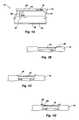
- FIGS. 1A-1D and 2 A- 2 Cdifferent types of bond pads 12 , 12 ′ that are typically used in semiconductor devices 10 , 10 ′ are depicted.
- FIG. 1Aa semiconductor device which includes copper bond pads 12 is shown. Copper bond pads 12 are typically formed on a passivation layer 14 of semiconductor device 10 and communicate with underlying, integrated circuitry of semiconductor device 10 .
- one or more generally downwardly extending conductive vias 16may establish electrical communication with conductive traces 18 , or “runners,” that, in turn, electrically communicate with the integrated circuitry of semiconductor device 10 .
- runners 18may lead to contact plugs 20 that provide a conductive link between runners 18 and a conductively doped silicon active-device region 22 of a transistor 24 of semiconductor device 10 .
- FIG. 1Aalso shows a back side passivation layer 34 of silicon dioxide that has been formed in accordance with teachings of the present invention.
- a back side passivation layer 34 of silicon dioxidehas been formed by a method of this invention to electrically insulate the back side 32 , preventing etching of bond pad 12 , as well as other possible damage to the circuits of semiconductor devices 10 by, for example, short circuiting during plating of bond pads 12 .
- a palladium activation layer 26may be formed thereon, as depicted in FIG. 1B , such as by the aggressive, acid-accelerated electroless plating processes described previously herein.
- a layer 28 of electrolessly deposited nickelmay then be formed on each bond pad 12 , as shown in FIG. 1C , followed by a layer 29 of immersion plated gold, as illustrated in FIG. 1D .
- the upper surface of semiconductor device 10may be further covered with a passivation and/or final package. It is understood that semiconductor device 10 , as shown, is part of a multi-semiconductor device wafer containing a plurality, e.g., hundreds, of semiconductor devices, although the method is applicable to a single discrete semiconductor device as well.
- FIG. 2Aillustrates a semiconductor device 10 ′ with each of the features of semiconductor device 10 ( FIG. 1A ).
- semiconductor device 10 ′includes another passivation layer 15 which overlies passivation layer 14 and each bond pad 12 exposed therethrough, a redistributed bond pad 12 ′ exposed through passivation layer 15 , and a conductive redistribution trace 13 extending between passivation layer 14 and passivation layer 15 from bond pad 12 to its corresponding redistributed bond pad 12 ′.
- Redistributed bond pad 12 ′may be configured to receive a discrete conductive element (not shown), such as a solder ball, and, therefore, may be formed from aluminum or another material suitable for securing such a discrete conductive element.
- Semiconductor device 10 ′also includes a back side passivation layer 34 on a back side thereof.
- a zincate processmay be conducted on redistributed bond pad 12 ′ ( FIG. 2B ) to form zinc grains 30 thereon, which facilitate adherence of an electrolessly deposited nickel layer 31 to redistributed bond pad 12 ′ ( FIG. 2C ).
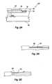
- FIG. 3one or more semiconductor wafers 40 are shown in a wafer carrier 42 for forming a back side silicon dioxide layer.
- the wafers 40are immersed in a supersaturated silicon dioxide solution 44 to precipitate, i.e., deposit a dense passivation layer 34 (see FIGS. 1A and 2A ) on the back side 32 of each wafer 40 .
- the depositionis specific to exposed silicon (and its oxide), and substantially does not plate out on bond pads 12 , 12 ′ ( FIGS. 1A and 2A , respectively) or on organic materials, such as photoresist.
- bond pads 12 , 12 ′may be precovered with tape to prevent deposition thereto.
- the back sides 32 of wafers 40are shown as being in a vertical position during immersion. However, the wafer orientation appears to be irrelevant to deposition rate or layer properties in this process, as long as constant exposure to the solution 44 is maintained.
- the supersaturated silicon dioxide solution 44is preferably stirred or recycled to prevent local depletion of silicon dioxide and provide fresh solution for coating the silicon surfaces.
- the wafers 40are extracted from the supersaturated silicon dioxide solution 44 and rinsed in rinsing apparatus 48 at reference 50 . Solution remaining on the wafer surfaces is washed away including any hexafluorosilicic acid, unattached precipitated silicon dioxide, and stable complex-ion BF 4 —.
- the rinsed wafers 40may be dried to prevent any dilution (though slight) of the subsequent plating solution 52 . However, there is no need to heat-treat the wafers 40 , such as is required by some layering processes.
- the bond pads 12 , 12 ′may then be plated with nickel or other metal in an electroless process, from plating solution 52 , in a plating represented at reference 54 .
- an electroless plating processmay include activation or other preparation of the surface of bond pads 12 , 12 ′, as explained previously herein (e.g., palladium activation of copper, zincating aluminum, etc.)
- a subsequent rinsing process 58is conducted using rinsing apparatus 56 before subsequent manufacturing processes, e.g., attachment of wires and packaging, are performed.
- Each of the indicated processesmay be comprised of several subprocesses.
- the aqueous reaction solution 44comprises an acid fluoride salt of the desired oxide, whether silicon dioxide, zirconium oxide, etc., and the solution is supersaturated in the desired oxide by the addition of a buffer, e.g., boric acid.
- the reactions, which take place in the formation of solution 44 , specific to silicon dioxide,are as follows: H 2 SiF 6 +2H 2 O SiO 2 +6 HF (Reaction A) H 3 BO 3 +4 HF BF 4 ⁇ -+H 30 + +2H 2 O (Reaction B)
- Reaction BHF produced in Reaction A is consumed by the addition of boric ion to produce a stable complex ionic species BF 4 ⁇ (as well as hydronium ion H 3 O + ), driving Reaction A to the right.
- the resultis supersaturation of the solution with respect to SiO 2 , which deposits on the exposed silicon surface (and silicon dioxide surface).
- one method for making a supersaturated silicon dioxide solutionis to first form an aqueous solution of hexafluorosilicic acid H 2 SiF 6 .
- the solutionis formed at a generally high concentration, for example, about 20-50 weight percent H 2 SiF 6 .
- Silicon dioxide (SiO 2 )is then added whereby, at equilibrium, the solution is saturated with respect to the oxide and contains hydrofluoric acid.
- Any silicon dioxide which precipitates, together with any other solids,is then preferably removed from the solution 44 with, for example, a 0.2 ⁇ m filter.
- the resultis a substantially solid-free solution 44 saturated in silicon dioxide.
- the solutionis then diluted with water.
- boric acidH 3 BO 3
- a silicon-surfaced semiconductor device, wafer, interposer or other deviceis immersed in the supersaturated solution 44 for deposition of a silicon dioxide layer. Following completion of such deposition, the coated device is rinsed to remove extraneous materials and further processed to completion.
- FIG. 5An alternate method of the present invention is shown in FIG. 5 , in which the initial concentrated hexafluorosilicic acid is first diluted with water prior to saturating with silicon dioxide. Following filtration, the method may follow substantially the same process flow shown in FIG. 4 .
- the thickness of silicon dioxide layerswhich may be formed by the methods of the invention range up to about 100 nm in a single deposition.
- a desired layer thickness for passivating the back side of a semiconductor wafermay be about 100 to 500 ⁇ (about 10 to about 50 nm), and other applications may use silicon dioxide layers of less than 100 ⁇ thickness.
- aluminummay be substituted for boric acid.
- the aluminumreacts with HF to form AlF 3 , driving reaction A to the right to supersaturate the solution in silicon dioxide.
- the inventionhas been described in terms of a passivation layer comprising silicon dioxide.
- Other oxidesmay be formed which will deposit onto an exposed silicon surface, having similar chemical routes.
- the layer-forming solutionmay be configured to deposit the oxides of zirconium, titanium, vanadium and even iron.
- a silicon dioxide-depositing solutionmay be formed by adding ammonia (NH 3 ) to a hexafluorosilicic acid solution whereby the solution becomes supersaturated in silicon dioxide.
- a passivating layer of silicon dioxideis formed on the back side of a semiconductor wafer, with many advantages over the prior art.
- the inventionalso encompasses the application of a passivating layer on the inner walls of a laser-formed via, on members such as carrier substrates, interposer substrates for flip-chip packaging, beneath interconnects for test packages, and the like.
- the method of the present inventionis particularly useful for passivating vias and microvias such as made by lasers through silicon.
- the method of the present inventiondeposits a uniform layer of oxide on the silicon surfaces of the via hole, without covering metallization to which the via hole may extend. Previous methods tend to produce uneven deposition so that, in order to assure complete coverage, the layer must in some places be much thicker than desired. The uneven coverage also unduly limited the diameter of microvia holes.
- Use of the present inventionavoids these problems, enabling uniform thin coatings within vias or microvias, formed easily, without prolonged exposure, and without covering nonsilicon surfaces.
Landscapes
- Engineering & Computer Science (AREA)
- Computer Hardware Design (AREA)
- Microelectronics & Electronic Packaging (AREA)
- Power Engineering (AREA)
- Physics & Mathematics (AREA)
- Chemical & Material Sciences (AREA)
- Condensed Matter Physics & Semiconductors (AREA)
- General Physics & Mathematics (AREA)
- Manufacturing & Machinery (AREA)
- Inorganic Chemistry (AREA)
- Ceramic Engineering (AREA)
- Thermal Sciences (AREA)
- General Chemical & Material Sciences (AREA)
- Chemical Kinetics & Catalysis (AREA)
- Materials Engineering (AREA)
- Mechanical Engineering (AREA)
- Metallurgy (AREA)
- Organic Chemistry (AREA)
- Chemically Coating (AREA)
- Formation Of Insulating Films (AREA)
Abstract
Description
- This application is a continuation of application Ser. No. 10/454,254, filed Jun. 3, 2003, pending, which is a continuation of application Ser. No. 10/218,268, filed Aug. 13, 2002, now U.S. Pat. No. 6,593,221, issued Jul. 15, 2003.
- 1. Field of the Invention
- The present invention relates to methods for electrically isolating dielectric materials. More particularly, the invention pertains to methods for electrical isolation, i.e., passivation of exposed silicon such as occurs on the back side of a semiconductor (SC) wafer comprising semiconductor devices or dice of a DRAM, SRAM, or other semiconductor die configuration. The invention also pertains to passivation of apparatus such as carrier substrates, interposer substrates for flip-chip packaging, conductive interconnects for test packages, and the like.
- 2. Background of Related Art
- Silicon is a basic material from which a broad range of semiconductor devices is composed. Silicon is a semiconductor while its oxidation product, silicon dioxide, acts as a dielectric (insulating) material. Thus, silicon dioxide is one of the classical insulators used to electrically isolate silicon from conductive leads, specific functional devices in electronic apparatus, and the atmosphere. Other insulators that are used include a variety of organic and inorganic compounds.
- The manufacture of semiconductor devices is performed by forming a plurality of the functional devices on a wafer and subsequently separating each semiconductor device by cutting along a pattern of saw lines crisscrossing the wafer. The various processes for forming a semiconductor device such as a DRAM or SRAM device may be generally characterized as including crystal growth, bare wafer formation, surface preparation, oxidation/nitridation, heat treatment, patterning, layer deposition, doping, metallization, and packaging. Typically, each of these processes includes several subprocesses.
- Layer deposition is generally performed by one of several processes, such as physical vapor deposition (PVD), chemical vapor deposition (CVD), sputtering, and electron-beam evaporation. In cases where the desired layer is to be an oxide of the base material, e.g., silicon dioxide, another common method includes the direct thermal oxidation of the existing silicon surface. Although the processes by which “growth” of a passivation layer on silicon by oxidizing the surface are highly developed, they have certain limitations. First, the rate of formation significantly slows as the layer thickness increases. Long times at high temperature are generally required to form thick layers, such as field oxides, surface passivation layers, and some masking oxide layers. Secondly, the growth rate is a function of wafer orientation. The <111> planes of a wafer have more silicon atoms than <100> planes, thus leading to faster formation of a SiO2layer. In addition, other factors affecting growth rates include the types and concentrations of doping materials in the silicon and the presence of polysilicon or impurities. Differential oxidation causes the resulting SiO2layer to have a stepped surface. It should be noted that the initial costs and operating costs of oxidation furnaces are high. Furthermore, a problem, which must be considered in thermal oxidation, is the formation of surface dislocations which may cause circuit problems.
- Another consideration relating to oxide growth is the inability to adequately passivate the lateral walls of a small via hole (such as a laser-formed microvia) of a multilayer device prior to deposition of a conductive material (such as tungsten) into the via hole. Present passivation methods for insulating the lateral walls of such small-diameter holes tend to produce uneven coverage, sometimes leading to either short circuits between the conductive via and the semiconductor or excessive filling of the via hole.
- In forming semiconductor devices, the electrically conductive bond pads on the active surface are grounded to the back side of the wafer. Unless neutralized by a passivation layer, the wafer back side has a net positive (+) charge.
- Bond pad formation typically includes applying a copper or aluminum base, then coating the base with another material so that wire bonds or conductive structures, such as solder, may be secured to the bond pad.
- In the case of bond pads to which bond wires are to be secured, copper is typically employed as the bond pad material. As copper forms a “slippery” oxide that is difficult to remove with a wire bonding capillary, nickel and gold adhesion layers are typically used. As copper alone will not initiate the adhesion of nickel thereto, a palladium “strike,” or seed layer, is typically formed prior to conducting an electroless nickel-plating process.
- Efforts have been made to use more aggressive plating chemistries in order to speed the plating rate and create a higher density coating at lower cost. Such chemistries, e.g., palladium chloride in hydrochloric acid, greatly enhance the plating rate and plate density. However, unless the wafer back side is first passivated, copper pads which communicate with the silicon substrate (e.g., pads that communicate with active-device regions of transistors) and, thus, which may form a circuit directly through the silicon substrate, may be attacked by the plating chemistry and dissolve in as little as several minutes of exposure, resulting in damaged pads with performance anomalies. In addition, bath chemicals will be inordinately consumed. The use of sulfuric acid in the palladium electroless plating solution may curb such an attack of the bond pads to some extent, but does not completely resolve this problem. Once the palladium strike has been formed, nickel may be plated onto the copper and palladium by way of electroless deposition processes, then a gold layer may be formed by immersion plating processes.
- Aluminum is typically used as the base metal for bond pads that will receive solder balls or other discrete conductive elements. As aluminum is not itself solderable, adhesion layers are typically deposited onto aluminum bond pads. Again, nickel is often used as such an adhesion layer. Nickel does not, however, adhere well to aluminum. A zincating process, usually “double zinc,” is typically used to facilitate adhesion of electrolessly deposited nickel to aluminum. If the back side of the silicon substrate upon which the bond pads are carried is not adequately passivated, the zincating process may etch the aluminum bond pads or deposit large zinc grains, which, in turn, adversely affects the subsequently deposited nickel layer.
- Moreover, in forming adhesion layers on both copper and aluminum bond pads, if the back side of the silicon substrate is not sufficiently passivated these nickel and gold layers may also be loosely deposited onto portions of the back side, which may result in the formation of particles in the plating baths, shortening the lives thereof and creating potential problems for downstream processes which are particle-sensitive, such as subsequent tape and probe processes.
- In the current state of the art, the general approach is to continue to use the more benign electroless plating method despite its overall cost.
- In an alternative approach, a back side coating such as a photoresist material is first applied to the wafer back side to cover the wafer's substrate material, e.g., silicon or germanium, and provide protection from a more aggressive plating chemistry. This method has further disadvantages in that the wafer is required to be removed from its work surface and inverted for resist application by a spin-on technique. Inversion and spin-on deposition require extra steps and equipment, are time consuming, and require forcibly clamped placement of the wafer's active surface on the flat surface of a vacuum hold-down tool, sometimes leading to physical damage to the semiconductor devices being formed on the wafer.
- In U.S. Pat. No. 6,022,814 of Mikoshiba et al., a method for forming a silicon dioxide layer is presented which includes the spin-coating of a resin compound having an O—COOH+O, Si—O, or Si—N backbone. After application, the coated surface is heat-treated to set the resin, followed by heating at between 250° C. and the glass transition point (˜450-500° C.) for 3 to 4 hours to form silicon dioxide. This method for forming a silicon dioxide layer suffers from the spin-coating disadvantages listed above. In addition, it requires significant furnace exposure at elevated temperatures.
- It is desired to have a semiconductor manufacturing method to plate bond pads to achieve uniform high-quality, high-density pads. It is further desired to have such bond pad formation without wafer inversion, while minimizing chemical usage, minimizing time consumption, and reducing the use of high-cost equipment. In addition, it is desired to have a method to produce such semiconductor devices at an optimally high yield.
- In a paper of Antti J. Niskanen, published prior to November 2000 and titled LIQUID PHASE DEPOSITION OF SILICON DIOXIDE, the author briefly summarizes tests to determine the possibility of liquid phase deposition of silicon dioxide. In a paper of Sampo Niskanen, dated November 2000 and titled DEVELOPMENT OF LIQUID PHASE DEPOSITION OF ZIRCONIUM OXIDE AND COMPARISON TO SILICON DIOXIDE, a summary is presented of tests comparing liquid phase depositions of zirconium dioxide and silicon dioxide to form thin films.
- The present invention is a method for selectively forming a dense layer of passivating oxide, e.g., silicon dioxide or zirconium oxide, onto an exposed semiconductor wafer surface, e.g., silicon or germanium. The layer is applied by submersion of the exposed semiconductor wafer surface in a liquid at low or ambient temperature. The passivation layer of easily controlled thickness may be formed in a limited amount of time. The method differs from conventional high-temperature thermal oxidation, chemical vapor deposition, and spin-on passivation methods, each of which requires sophisticated equipment and high manpower costs. The method does not require inversion of a semiconductor wafer such as required by prior art back side deposition using spin-on deposition, nor does it require protracted heating at a high temperature to cure the layer.
- The present invention is directed to the application of a silicon dioxide layer on an exposed silicon layer. The deposition is selective to silicon/silicon dioxide and may be performed by exposure to a liquid phase composition in a bath at room temperature or a temperature somewhat above room temperature, e.g., up to about 50° C. The liquid phase composition is supersaturated in silicon dioxide. The silicon dioxide deposition rate is not self-limiting, that is, it does not depend upon the layer thickness. The deposition rate may be readily controlled to provide repeatedly uniform layer thickness. Thus, for example, the method may be used to passivate the back side of a wafer or other semiconductor substrate without inverting the wafer or substrate. The method is specific to the base substrate, e.g., silicon and its oxide. Further exclusion of oxide from other surfaces may be assured by, for example, covering such surfaces with tape. Any silicon dioxide pre-existing on the silicon surface may be first removed or, alternatively, left in place for oxide deposit thereover.
- In one embodiment of the invention, a silicon wafer is formed for the purpose of producing a plurality of semiconductor devices, e.g., DRAM semiconductor devices, SRAM semiconductor devices or other types of semiconductor devices. After forming the semiconductor devices on the active surface of the wafer, covering the semiconductor devices with an insulative layer, and forming conductive traces on each semiconductor device, bond pads are formed to connect the traces (generally copper, aluminum, or alloys thereof) to external connectors (via wire bonds, for example). Prior to forming the bond pads by an electroless method, the wafer is submerged in a bath of supersaturated silicon dioxide at room temperature or somewhat higher, up to about 50° C., by which exposed silicon on the wafer back side becomes covered with a passivating layer of silicon dioxide.
- The exposed copper or aluminum metallization at each bond pad location may then be coated with immersion palladium or zinc, followed by an electroless nickel and, optionally, immersion gold, in a bath to form pads amenable to soldering or another joint with an external conductor. For example, the bond pads may then be coated with gold or solder-bonded to conductive wires. The overall process results in devices which are produced at reduced time and expense and which are more reliable than those currently produced.
- The liquid bath is supersaturated with respect to an oxide of a material which is capable of forming a hexafluoro salt. This includes, for example, silicon, zirconium, iron, and vanadium. In this invention, the primary passivation material of interest is silicon dioxide, but other oxides may also be used.
- The liquid bath of saturated silicon dioxide is formed by adding silicon dioxide and water to hexafluorosilicic acid H2SiF6. The solution may be diluted with water either before or after silicon dioxide is added to the saturation point. Boric acid (H3BO3) is then added to supersaturate the liquid in silicon dioxide. The silicon dioxide selectively precipitates onto the silicon/silicon oxide surface as a dense cohesive layer of uniform thickness.
- In addition to the application for enhancing bond pad plating, the method of the invention is applicable to the passivation of vias and microvias and to forming other layers on exposed silicon, such as on a semiconductor device wafer, interposer wafer, etc.
- The nature of the present invention as well as other embodiments thereof may be more clearly understood by reference to the following detailed description of the invention, to the appended claims, and to the several drawings herein, wherein:
FIGS. 1A-1D are schematic cross-sectional representations through a semiconductor device, the back side of which is depicted with a passivation layer applied in accordance with a method of the present invention;FIGS. 2A-2C are schematic cross-sectional representations through another semiconductor device, the back side of which is depicted with a passivation layer applied in accordance with teachings of the present invention;FIG. 3 is a schematic representation of a method for forming a passivation layer on silicon in accordance with the present invention and subsequent plating of bond pads of a semiconductor device;FIG. 4 is a representation of an exemplary embodiment of a method for forming a supersaturated silicon dioxide solution for passivating a silicon surface in accordance with a method of the present invention; andFIG. 5 is a representation of the processes of another embodiment of forming a supersaturated silicon dioxide solution for passivating a silicon surface in accordance with a method of the present invention.- With reference to
FIGS. 1A-1D and2A-2C, different types ofbond pads semiconductor devices FIG. 1A , a semiconductor device which includescopper bond pads 12 is shown.Copper bond pads 12 are typically formed on apassivation layer 14 ofsemiconductor device 10 and communicate with underlying, integrated circuitry ofsemiconductor device 10. By way of example, one or more generally downwardly extendingconductive vias 16 may establish electrical communication withconductive traces 18, or “runners,” that, in turn, electrically communicate with the integrated circuitry ofsemiconductor device 10. For example,runners 18 may lead to contact plugs20 that provide a conductive link betweenrunners 18 and a conductively doped silicon active-device region22 of atransistor 24 ofsemiconductor device 10. - In order to use a rapid electroless plating method to plate
bond pads semiconductor device 10, it is necessary to insulate the net positive (+) charge on the semiconductor device'sback side 32.FIG. 1A also shows a backside passivation layer 34 of silicon dioxide that has been formed in accordance with teachings of the present invention. InFIG. 1A , a backside passivation layer 34 of silicon dioxide has been formed by a method of this invention to electrically insulate theback side 32, preventing etching ofbond pad 12, as well as other possible damage to the circuits ofsemiconductor devices 10 by, for example, short circuiting during plating ofbond pads 12. - Once back
side passivation layer 34 has been formed, apalladium activation layer 26 may be formed thereon, as depicted inFIG. 1B , such as by the aggressive, acid-accelerated electroless plating processes described previously herein. Alayer 28 of electrolessly deposited nickel may then be formed on eachbond pad 12, as shown inFIG. 1C , followed by alayer 29 of immersion plated gold, as illustrated inFIG. 1D . Following plating ofbond pads 12, the upper surface ofsemiconductor device 10 may be further covered with a passivation and/or final package. It is understood thatsemiconductor device 10, as shown, is part of a multi-semiconductor device wafer containing a plurality, e.g., hundreds, of semiconductor devices, although the method is applicable to a single discrete semiconductor device as well. FIG. 2A illustrates asemiconductor device 10′ with each of the features of semiconductor device10 (FIG. 1A ). In addition,semiconductor device 10′ includes anotherpassivation layer 15 which overliespassivation layer 14 and eachbond pad 12 exposed therethrough, a redistributedbond pad 12′ exposed throughpassivation layer 15, and aconductive redistribution trace 13 extending betweenpassivation layer 14 andpassivation layer 15 frombond pad 12 to its corresponding redistributedbond pad 12′. Redistributedbond pad 12′ may be configured to receive a discrete conductive element (not shown), such as a solder ball, and, therefore, may be formed from aluminum or another material suitable for securing such a discrete conductive element.Semiconductor device 10′ also includes a backside passivation layer 34 on a back side thereof.- As shown in
FIGS. 2B and 2C , a zincate process may be conducted on redistributedbond pad 12′ (FIG. 2B ) to formzinc grains 30 thereon, which facilitate adherence of an electrolessly depositednickel layer 31 to redistributedbond pad 12′ (FIG. 2C ). - Turning now to
FIG. 3 , one ormore semiconductor wafers 40 are shown in awafer carrier 42 for forming a back side silicon dioxide layer. First, atreference 46, thewafers 40 are immersed in a supersaturatedsilicon dioxide solution 44 to precipitate, i.e., deposit a dense passivation layer34 (seeFIGS. 1A and 2A ) on theback side 32 of eachwafer 40. The deposition is specific to exposed silicon (and its oxide), and substantially does not plate out onbond pads FIGS. 1A and 2A , respectively) or on organic materials, such as photoresist. However, in the event that minute quantities of silicon dioxide are found to adhere tobond pads wafers 40 are shown as being in a vertical position during immersion. However, the wafer orientation appears to be irrelevant to deposition rate or layer properties in this process, as long as constant exposure to thesolution 44 is maintained. - In the
submersion process 46, the following factors are controlled: - a. The concentration of components in the supersaturated
silicon dioxide solution 44 is controlled to provide sufficient silicon dioxide for the desired layer depth and insulative value. Inasmuch as deposition is specific to surfaces of silicon and its oxide, the required solution composition may be readily calculated. - b. During submersion, the solution temperature generally may be between about room temperature and about 50° C. While the temperature may be even higher, e.g., up to about 90° C., there may be no reason to control the temperature at much above room temperature in most cases.
- c. The time of submersion is relatively short, typically on the order of about 1 minute to about 60 minutes, depending upon the particular application. Some applications may require longer immersion times to achieve the desired layer thickness. The deposition rate has been found to be independent of the layer thickness, but may attain a “steady-state” thickness upon long-term exposure.
- d. The pressure at which the exposure takes place is preferably atmospheric, or nearly so, requiring no special control.
- a. The concentration of components in the supersaturated
- During submersion of the
wafers 40, the supersaturatedsilicon dioxide solution 44 is preferably stirred or recycled to prevent local depletion of silicon dioxide and provide fresh solution for coating the silicon surfaces. - Following formation of the back
side passivation layer 34, thewafers 40 are extracted from the supersaturatedsilicon dioxide solution 44 and rinsed in rinsingapparatus 48 atreference 50. Solution remaining on the wafer surfaces is washed away including any hexafluorosilicic acid, unattached precipitated silicon dioxide, and stable complex-ion BF4—. - Optionally, the rinsed
wafers 40 may be dried to prevent any dilution (though slight) of thesubsequent plating solution 52. However, there is no need to heat-treat thewafers 40, such as is required by some layering processes. - As shown in
FIG. 3 , thebond pads FIGS. 1A and 2A ) may then be plated with nickel or other metal in an electroless process, from platingsolution 52, in a plating represented atreference 54. Of course, such an electroless plating process may include activation or other preparation of the surface ofbond pads subsequent rinsing process 58 is conducted usingrinsing apparatus 56 before subsequent manufacturing processes, e.g., attachment of wires and packaging, are performed. Each of the indicated processes may be comprised of several subprocesses. - Alternative methods for forming the supersaturated
silicon dioxide solution 44 are depicted in drawingFIGS. 3 and 4 . As shown in the drawing figures, theaqueous reaction solution 44 comprises an acid fluoride salt of the desired oxide, whether silicon dioxide, zirconium oxide, etc., and the solution is supersaturated in the desired oxide by the addition of a buffer, e.g., boric acid. The reactions, which take place in the formation ofsolution 44, specific to silicon dioxide, are as follows:
H2SiF6+2H2OSiO2+6 HF (Reaction A)
H3BO3+4 HFBF4−-+H30++2H2O (Reaction B) - It can be seen that in Reaction B, HF produced in Reaction A is consumed by the addition of boric ion to produce a stable complex ionic species BF4− (as well as hydronium ion H3O+), driving Reaction A to the right. The result is supersaturation of the solution with respect to SiO2, which deposits on the exposed silicon surface (and silicon dioxide surface).
- As shown in drawing
FIG. 3 , one method for making a supersaturated silicon dioxide solution is to first form an aqueous solution of hexafluorosilicic acid H2SiF6. The solution is formed at a generally high concentration, for example, about 20-50 weight percent H2SiF6. Silicon dioxide (SiO2) is then added whereby, at equilibrium, the solution is saturated with respect to the oxide and contains hydrofluoric acid. - Any silicon dioxide which precipitates, together with any other solids, is then preferably removed from the
solution 44 with, for example, a 0.2 μm filter. The result is a substantially solid-free solution 44 saturated in silicon dioxide. - The solution is then diluted with water. To this diluted
solution 44 is added boric acid (H3BO3) at a concentration which will tie up the HF to supersaturate the solution in silicon dioxide. In this invention, a silicon-surfaced semiconductor device, wafer, interposer or other device is immersed in thesupersaturated solution 44 for deposition of a silicon dioxide layer. Following completion of such deposition, the coated device is rinsed to remove extraneous materials and further processed to completion. - An alternate method of the present invention is shown in
FIG. 5 , in which the initial concentrated hexafluorosilicic acid is first diluted with water prior to saturating with silicon dioxide. Following filtration, the method may follow substantially the same process flow shown inFIG. 4 . - The thickness of silicon dioxide layers which may be formed by the methods of the invention range up to about 100 nm in a single deposition. Typically, a desired layer thickness for passivating the back side of a semiconductor wafer may be about 100 to 500 Å (about 10 to about 50 nm), and other applications may use silicon dioxide layers of less than 100 Å thickness.
- It should be noted that in either of the foregoing methods of the present invention of
FIGS. 4 and 5 , aluminum may be substituted for boric acid. In this case, the aluminum reacts with HF to form AlF3, driving reaction A to the right to supersaturate the solution in silicon dioxide. - Thus far, the invention has been described in terms of a passivation layer comprising silicon dioxide. Other oxides may be formed which will deposit onto an exposed silicon surface, having similar chemical routes. For example, the layer-forming solution may be configured to deposit the oxides of zirconium, titanium, vanadium and even iron.
- In another embodiment of the method of the present invention, a silicon dioxide-depositing solution may be formed by adding ammonia (NH3) to a hexafluorosilicic acid solution whereby the solution becomes supersaturated in silicon dioxide.
- In a first embodiment, already described, a passivating layer of silicon dioxide is formed on the back side of a semiconductor wafer, with many advantages over the prior art. The invention also encompasses the application of a passivating layer on the inner walls of a laser-formed via, on members such as carrier substrates, interposer substrates for flip-chip packaging, beneath interconnects for test packages, and the like. The method of the present invention is particularly useful for passivating vias and microvias such as made by lasers through silicon. The method of the present invention deposits a uniform layer of oxide on the silicon surfaces of the via hole, without covering metallization to which the via hole may extend. Previous methods tend to produce uneven deposition so that, in order to assure complete coverage, the layer must in some places be much thicker than desired. The uneven coverage also unduly limited the diameter of microvia holes. Use of the present invention avoids these problems, enabling uniform thin coatings within vias or microvias, formed easily, without prolonged exposure, and without covering nonsilicon surfaces.
- Although the foregoing description contains many specifics, these should not be construed as limiting the scope of the present invention, but merely as providing illustrations of some exemplary embodiments. Similarly, other embodiments of the invention may be devised which do not depart from the spirit or scope of the present invention. Features from different embodiments may be employed in combination. The scope of the invention is, therefore, indicated and limited only by the appended claims and their legal equivalents, rather than by the foregoing description. All additions, deletions, and modifications to the invention, as disclosed herein, which fall within the meaning and scope of the claims are to be embraced thereby.

Claims (37)
Priority Applications (1)
| Application Number | Priority Date | Filing Date | Title |
|---|---|---|---|
| US11/087,212US7312164B2 (en) | 2002-08-13 | 2005-03-23 | Selective passivation of exposed silicon |
Applications Claiming Priority (3)
| Application Number | Priority Date | Filing Date | Title |
|---|---|---|---|
| US10/218,268US6593221B1 (en) | 2002-08-13 | 2002-08-13 | Selective passivation of exposed silicon |
| US10/454,254US6905953B2 (en) | 2002-08-13 | 2003-06-03 | Selective passivation of exposed silicon |
| US11/087,212US7312164B2 (en) | 2002-08-13 | 2005-03-23 | Selective passivation of exposed silicon |
Related Parent Applications (1)
| Application Number | Title | Priority Date | Filing Date |
|---|---|---|---|
| US10/454,254ContinuationUS6905953B2 (en) | 2002-08-13 | 2003-06-03 | Selective passivation of exposed silicon |
Publications (2)
| Publication Number | Publication Date |
|---|---|
| US20050164500A1true US20050164500A1 (en) | 2005-07-28 |
| US7312164B2 US7312164B2 (en) | 2007-12-25 |
Family
ID=22814435
Family Applications (5)
| Application Number | Title | Priority Date | Filing Date |
|---|---|---|---|
| US10/218,268Expired - LifetimeUS6593221B1 (en) | 2002-08-13 | 2002-08-13 | Selective passivation of exposed silicon |
| US10/454,254Expired - LifetimeUS6905953B2 (en) | 2002-08-13 | 2003-06-03 | Selective passivation of exposed silicon |
| US10/454,256Expired - LifetimeUS7190052B2 (en) | 2002-08-13 | 2003-06-03 | Semiconductor devices with oxide coatings selectively positioned over exposed features including semiconductor material |
| US11/087,212Expired - LifetimeUS7312164B2 (en) | 2002-08-13 | 2005-03-23 | Selective passivation of exposed silicon |
| US11/717,435AbandonedUS20070170551A1 (en) | 2002-08-13 | 2007-03-12 | Semiconductor devices with oxide coatings selectively positioned over exposed features including semiconductor material and solutions for forming the coatings |
Family Applications Before (3)
| Application Number | Title | Priority Date | Filing Date |
|---|---|---|---|
| US10/218,268Expired - LifetimeUS6593221B1 (en) | 2002-08-13 | 2002-08-13 | Selective passivation of exposed silicon |
| US10/454,254Expired - LifetimeUS6905953B2 (en) | 2002-08-13 | 2003-06-03 | Selective passivation of exposed silicon |
| US10/454,256Expired - LifetimeUS7190052B2 (en) | 2002-08-13 | 2003-06-03 | Semiconductor devices with oxide coatings selectively positioned over exposed features including semiconductor material |
Family Applications After (1)
| Application Number | Title | Priority Date | Filing Date |
|---|---|---|---|
| US11/717,435AbandonedUS20070170551A1 (en) | 2002-08-13 | 2007-03-12 | Semiconductor devices with oxide coatings selectively positioned over exposed features including semiconductor material and solutions for forming the coatings |
Country Status (1)
| Country | Link |
|---|---|
| US (5) | US6593221B1 (en) |
Cited By (19)
| Publication number | Priority date | Publication date | Assignee | Title |
|---|---|---|---|---|
| US7413979B2 (en) | 2003-11-13 | 2008-08-19 | Micron Technology, Inc. | Methods for forming vias in microelectronic devices, and methods for packaging microelectronic devices |
| US7425499B2 (en) | 2004-08-24 | 2008-09-16 | Micron Technology, Inc. | Methods for forming interconnects in vias and microelectronic workpieces including such interconnects |
| US7435913B2 (en) | 2004-08-27 | 2008-10-14 | Micron Technology, Inc. | Slanted vias for electrical circuits on circuit boards and other substrates |
| US7531453B2 (en) | 2004-06-29 | 2009-05-12 | Micron Technology, Inc. | Microelectronic devices and methods for forming interconnects in microelectronic devices |
| US20090146312A1 (en)* | 2007-12-06 | 2009-06-11 | Micron Technology, Inc. | Methods for forming interconnects in microelectronic workpieces and microelectronic workpieces formed using such methods |
| US20090166846A1 (en)* | 2007-12-28 | 2009-07-02 | Micron Technology, Inc. | Pass-through 3d interconnect for microelectronic dies and associated systems and methods |
| US7589008B2 (en) | 2004-12-30 | 2009-09-15 | Micron Technology, Inc. | Methods for forming interconnects in microelectronic workpieces and microelectronic workpieces formed using such methods |
| US20090283898A1 (en)* | 2008-05-15 | 2009-11-19 | Janzen Jeffery W | Disabling electrical connections using pass-through 3d interconnects and associated systems and methods |
| US7622377B2 (en) | 2005-09-01 | 2009-11-24 | Micron Technology, Inc. | Microfeature workpiece substrates having through-substrate vias, and associated methods of formation |
| US7629249B2 (en) | 2006-08-28 | 2009-12-08 | Micron Technology, Inc. | Microfeature workpieces having conductive interconnect structures formed by chemically reactive processes, and associated systems and methods |
| US7683458B2 (en) | 2004-09-02 | 2010-03-23 | Micron Technology, Inc. | Through-wafer interconnects for photoimager and memory wafers |
| US7749899B2 (en) | 2006-06-01 | 2010-07-06 | Micron Technology, Inc. | Microelectronic workpieces and methods and systems for forming interconnects in microelectronic workpieces |
| US7795134B2 (en) | 2005-06-28 | 2010-09-14 | Micron Technology, Inc. | Conductive interconnect structures and formation methods using supercritical fluids |
| US7830018B2 (en) | 2007-08-31 | 2010-11-09 | Micron Technology, Inc. | Partitioned through-layer via and associated systems and methods |
| US7863187B2 (en) | 2005-09-01 | 2011-01-04 | Micron Technology, Inc. | Microfeature workpieces and methods for forming interconnects in microfeature workpieces |
| US7902643B2 (en) | 2006-08-31 | 2011-03-08 | Micron Technology, Inc. | Microfeature workpieces having interconnects and conductive backplanes, and associated systems and methods |
| US7915736B2 (en) | 2005-09-01 | 2011-03-29 | Micron Technology, Inc. | Microfeature workpieces and methods for forming interconnects in microfeature workpieces |
| US8084866B2 (en) | 2003-12-10 | 2011-12-27 | Micron Technology, Inc. | Microelectronic devices and methods for filling vias in microelectronic devices |
| US8536485B2 (en) | 2004-05-05 | 2013-09-17 | Micron Technology, Inc. | Systems and methods for forming apertures in microfeature workpieces |
Families Citing this family (16)
| Publication number | Priority date | Publication date | Assignee | Title |
|---|---|---|---|---|
| US6593221B1 (en)* | 2002-08-13 | 2003-07-15 | Micron Technology, Inc. | Selective passivation of exposed silicon |
| US6825564B2 (en)* | 2002-08-21 | 2004-11-30 | Micron Technology, Inc. | Nickel bonding cap over copper metalized bondpads |
| US6969638B2 (en)* | 2003-06-27 | 2005-11-29 | Texas Instruments Incorporated | Low cost substrate for an integrated circuit device with bondpads free of plated gold |
| US20050001316A1 (en)* | 2003-07-01 | 2005-01-06 | Motorola, Inc. | Corrosion-resistant bond pad and integrated device |
| US7081372B2 (en)* | 2003-07-09 | 2006-07-25 | Chartered Semiconductor Manufacturing Ltd. | Aluminum cap with electroless nickel/immersion gold |
| US7425767B2 (en)* | 2004-07-14 | 2008-09-16 | Megica Corporation | Chip structure with redistribution traces |
| US7279407B2 (en) | 2004-09-02 | 2007-10-09 | Micron Technology, Inc. | Selective nickel plating of aluminum, copper, and tungsten structures |
| US7488680B2 (en) | 2005-08-30 | 2009-02-10 | International Business Machines Corporation | Conductive through via process for electronic device carriers |
| JP4937772B2 (en)* | 2007-01-22 | 2012-05-23 | 東京エレクトロン株式会社 | Substrate processing method |
| KR100809726B1 (en)* | 2007-05-14 | 2008-03-06 | 삼성전자주식회사 | An alignment mark, a semiconductor chip having the alignment mark, a semiconductor package including the semiconductor chip, and methods of manufacturing the semiconductor chip and the semiconductor package |
| KR20100060309A (en)* | 2008-11-27 | 2010-06-07 | 주식회사 동부하이텍 | A semiconductor device |
| TWI419284B (en)* | 2010-05-26 | 2013-12-11 | Chipmos Technologies Inc | Chip bump structure and method for forming chip bump structure |
| US8603924B2 (en) | 2010-10-19 | 2013-12-10 | Taiwan Semiconductor Manufacturing Company, Ltd. | Methods of forming gate dielectric material |
| CN103563048A (en) | 2011-03-29 | 2014-02-05 | 奈特考尔技术公司 | Method for controlling thickness of silicon oxide film |
| JP2014060185A (en) | 2012-09-14 | 2014-04-03 | Toshiba Corp | Semiconductor device manufacturing method and semiconductor device |
| JP7457537B2 (en)* | 2020-03-06 | 2024-03-28 | 関東化学株式会社 | Composition for electroless gold plating |
Citations (22)
| Publication number | Priority date | Publication date | Assignee | Title |
|---|---|---|---|---|
| US4599792A (en)* | 1984-06-15 | 1986-07-15 | International Business Machines Corporation | Buried field shield for an integrated circuit |
| US5192714A (en)* | 1990-02-14 | 1993-03-09 | Kabushiki Kaisha Toshiba | Method of manufacturing a multilayered metallization structure in which the conductive layer and insulating layer are selectively deposited |
| US5256593A (en)* | 1991-10-03 | 1993-10-26 | Kabushiki Kaisha Toshiba | Method of making isolation structure in semiconductor integrated circuit device |
| US5365112A (en)* | 1991-10-14 | 1994-11-15 | Kabushiki Kaisha Toshiba | Semiconductor integrated circuit device having an improved bonding pad structure |
| US5395645A (en)* | 1991-08-12 | 1995-03-07 | Kabushiki Kaisha Toshiba | Method for forming a silicon oxide film on a silicon waffer |
| US5429956A (en)* | 1994-09-30 | 1995-07-04 | United Microelectronics Corporation | Method for fabricating a field effect transistor with a self-aligned anti-punchthrough implant channel |
| US5516721A (en)* | 1993-12-23 | 1996-05-14 | International Business Machines Corporation | Isolation structure using liquid phase oxide deposition |
| US5683946A (en)* | 1995-12-01 | 1997-11-04 | National Science Counsil | Method for manufacturing fluorinated gate oxide layer |
| US5776829A (en)* | 1994-11-22 | 1998-07-07 | Nec Corporation | Method for forming multilevel interconnections in a semiconductor device |
| US6022814A (en)* | 1997-02-13 | 2000-02-08 | Kabushiki Kaisha Toshiba | Material of forming silicon oxide film, silicon oxide film, method of forming silicon oxide film and semiconductor element |
| US6045877A (en)* | 1997-07-28 | 2000-04-04 | Massachusetts Institute Of Technology | Pyrolytic chemical vapor deposition of silicone films |
| US6130116A (en)* | 1996-12-13 | 2000-10-10 | Tessera, Inc. | Method of encapsulating a microelectronic assembly utilizing a barrier |
| US6174824B1 (en)* | 1999-03-04 | 2001-01-16 | International Business Machines Corporation | Post-processing a completed semiconductor device |
| US6197110B1 (en)* | 1998-04-30 | 2001-03-06 | National Science Counsel | Mass production of silicon dioxide film by liquid phase deposition method |
| US6251753B1 (en)* | 1999-11-23 | 2001-06-26 | Ching-Fa Yeh | Method of sidewall capping for degradation-free damascene trenches of low dielectric constant dielectric by selective liquid-phase deposition |
| US6294832B1 (en)* | 2000-04-10 | 2001-09-25 | National Science Council | Semiconductor device having structure of copper interconnect/barrier dielectric liner/low-k dielectric trench and its fabrication method |
| US6335224B1 (en)* | 2000-05-16 | 2002-01-01 | Sandia Corporation | Protection of microelectronic devices during packaging |
| US6399494B1 (en)* | 2000-11-28 | 2002-06-04 | Oki Electric Industry Co., Ltd. | Method of making a semiconductor device |
| US20020090813A1 (en)* | 2001-01-08 | 2002-07-11 | United Microelectronics Corp. | Method for forming a dual damascene opening by liquid phase deposition |
| US6593221B1 (en)* | 2002-08-13 | 2003-07-15 | Micron Technology, Inc. | Selective passivation of exposed silicon |
| US20030201536A1 (en)* | 2002-04-26 | 2003-10-30 | Nec Electronics Corporation | Semiconductor device and manufacturing process therefor as well as plating solution |
| US6671947B2 (en)* | 1999-06-28 | 2004-01-06 | Intel Corporation | Method of making an interposer |
Family Cites Families (13)
| Publication number | Priority date | Publication date | Assignee | Title |
|---|---|---|---|---|
| US2526593A (en)* | 1948-04-15 | 1950-10-17 | Eaton Mfg Co | Hydraulic compensating mechanism |
| NL8201925A (en)* | 1982-05-11 | 1983-12-01 | Unie Van Kunstmestfab Bv | METHOD FOR PREPARING PURE SILICON DIOXIDE AND SILICON DIOXIDE OBTAINED BY THIS METHOD |
| DE3332995A1 (en)* | 1983-07-14 | 1985-01-24 | Nippon Sheet Glass Co. Ltd., Osaka | METHOD FOR PRODUCING A SILICON DIOXIDE COATING |
| EP0510191A4 (en)* | 1990-10-25 | 1993-03-03 | Nippon Sheet Glass Co., Ltd. | Process for preparing silicon dioxide coating |
| KR0134108B1 (en)* | 1994-06-30 | 1998-04-20 | 김주용 | Manufacturing method of semiconductor device |
| US5525535A (en)* | 1995-07-26 | 1996-06-11 | United Microelectronics Corporation | Method for making doped well and field regions on semiconductor substrates for field effect transistors using liquid phase deposition of oxides |
| US5920780A (en)* | 1997-01-31 | 1999-07-06 | Mosel Vitelic Incorporated | Method of forming a self aligned contact (SAC) window |
| US6004886A (en)* | 1997-10-30 | 1999-12-21 | National Science Council | Liquid phase deposition method for forming silicon dioxide film on HGCDTE or other II-VI semiconductor substrate |
| US6482751B2 (en)* | 1999-04-01 | 2002-11-19 | Winbond Electronics Corp. | Titanium dioxide layer serving as a mask and its removed method |
| US6316981B1 (en)* | 2000-03-13 | 2001-11-13 | Intel Corporation | Signal distribution network on backside of substrate |
| US6879492B2 (en)* | 2001-03-28 | 2005-04-12 | International Business Machines Corporation | Hyperbga buildup laminate |
| US6962147B2 (en)* | 2001-10-23 | 2005-11-08 | Micron Technology Inc | Dicing saw blade positioning apparatus and methods independent of blade thickness via constrained biasing elements |
| US6919011B2 (en)* | 2001-12-27 | 2005-07-19 | The Hong Kong Polytechnic University | Complex waveform electroplating |
- 2002
- 2002-08-13USUS10/218,268patent/US6593221B1/ennot_activeExpired - Lifetime
- 2003
- 2003-06-03USUS10/454,254patent/US6905953B2/ennot_activeExpired - Lifetime
- 2003-06-03USUS10/454,256patent/US7190052B2/ennot_activeExpired - Lifetime
- 2005
- 2005-03-23USUS11/087,212patent/US7312164B2/ennot_activeExpired - Lifetime
- 2007
- 2007-03-12USUS11/717,435patent/US20070170551A1/ennot_activeAbandoned
Patent Citations (23)
| Publication number | Priority date | Publication date | Assignee | Title |
|---|---|---|---|---|
| US4599792A (en)* | 1984-06-15 | 1986-07-15 | International Business Machines Corporation | Buried field shield for an integrated circuit |
| US5192714A (en)* | 1990-02-14 | 1993-03-09 | Kabushiki Kaisha Toshiba | Method of manufacturing a multilayered metallization structure in which the conductive layer and insulating layer are selectively deposited |
| US5395645A (en)* | 1991-08-12 | 1995-03-07 | Kabushiki Kaisha Toshiba | Method for forming a silicon oxide film on a silicon waffer |
| US5256593A (en)* | 1991-10-03 | 1993-10-26 | Kabushiki Kaisha Toshiba | Method of making isolation structure in semiconductor integrated circuit device |
| US5365112A (en)* | 1991-10-14 | 1994-11-15 | Kabushiki Kaisha Toshiba | Semiconductor integrated circuit device having an improved bonding pad structure |
| US5516721A (en)* | 1993-12-23 | 1996-05-14 | International Business Machines Corporation | Isolation structure using liquid phase oxide deposition |
| US5429956A (en)* | 1994-09-30 | 1995-07-04 | United Microelectronics Corporation | Method for fabricating a field effect transistor with a self-aligned anti-punchthrough implant channel |
| US5776829A (en)* | 1994-11-22 | 1998-07-07 | Nec Corporation | Method for forming multilevel interconnections in a semiconductor device |
| US5683946A (en)* | 1995-12-01 | 1997-11-04 | National Science Counsil | Method for manufacturing fluorinated gate oxide layer |
| US6130116A (en)* | 1996-12-13 | 2000-10-10 | Tessera, Inc. | Method of encapsulating a microelectronic assembly utilizing a barrier |
| US6022814A (en)* | 1997-02-13 | 2000-02-08 | Kabushiki Kaisha Toshiba | Material of forming silicon oxide film, silicon oxide film, method of forming silicon oxide film and semiconductor element |
| US6045877A (en)* | 1997-07-28 | 2000-04-04 | Massachusetts Institute Of Technology | Pyrolytic chemical vapor deposition of silicone films |
| US6197110B1 (en)* | 1998-04-30 | 2001-03-06 | National Science Counsel | Mass production of silicon dioxide film by liquid phase deposition method |
| US6174824B1 (en)* | 1999-03-04 | 2001-01-16 | International Business Machines Corporation | Post-processing a completed semiconductor device |
| US6671947B2 (en)* | 1999-06-28 | 2004-01-06 | Intel Corporation | Method of making an interposer |
| US6251753B1 (en)* | 1999-11-23 | 2001-06-26 | Ching-Fa Yeh | Method of sidewall capping for degradation-free damascene trenches of low dielectric constant dielectric by selective liquid-phase deposition |
| US6294832B1 (en)* | 2000-04-10 | 2001-09-25 | National Science Council | Semiconductor device having structure of copper interconnect/barrier dielectric liner/low-k dielectric trench and its fabrication method |
| US6335224B1 (en)* | 2000-05-16 | 2002-01-01 | Sandia Corporation | Protection of microelectronic devices during packaging |
| US6399494B1 (en)* | 2000-11-28 | 2002-06-04 | Oki Electric Industry Co., Ltd. | Method of making a semiconductor device |
| US20020090813A1 (en)* | 2001-01-08 | 2002-07-11 | United Microelectronics Corp. | Method for forming a dual damascene opening by liquid phase deposition |
| US20030201536A1 (en)* | 2002-04-26 | 2003-10-30 | Nec Electronics Corporation | Semiconductor device and manufacturing process therefor as well as plating solution |
| US6593221B1 (en)* | 2002-08-13 | 2003-07-15 | Micron Technology, Inc. | Selective passivation of exposed silicon |
| US6905953B2 (en)* | 2002-08-13 | 2005-06-14 | Micron Technology, Inc. | Selective passivation of exposed silicon |
Cited By (54)
| Publication number | Priority date | Publication date | Assignee | Title |
|---|---|---|---|---|
| US7413979B2 (en) | 2003-11-13 | 2008-08-19 | Micron Technology, Inc. | Methods for forming vias in microelectronic devices, and methods for packaging microelectronic devices |
| US9653420B2 (en) | 2003-11-13 | 2017-05-16 | Micron Technology, Inc. | Microelectronic devices and methods for filling vias in microelectronic devices |
| US7759800B2 (en) | 2003-11-13 | 2010-07-20 | Micron Technology, Inc. | Microelectronics devices, having vias, and packaged microelectronic devices having vias |
| US8748311B2 (en) | 2003-12-10 | 2014-06-10 | Micron Technology, Inc. | Microelectronic devices and methods for filing vias in microelectronic devices |
| US11177175B2 (en) | 2003-12-10 | 2021-11-16 | Micron Technology, Inc. | Microelectronic devices and methods for filling vias in microelectronic devices |
| US8084866B2 (en) | 2003-12-10 | 2011-12-27 | Micron Technology, Inc. | Microelectronic devices and methods for filling vias in microelectronic devices |
| US10010977B2 (en) | 2004-05-05 | 2018-07-03 | Micron Technology, Inc. | Systems and methods for forming apertures in microfeature workpieces |
| US8686313B2 (en) | 2004-05-05 | 2014-04-01 | Micron Technology, Inc. | System and methods for forming apertures in microfeature workpieces |
| US8664562B2 (en) | 2004-05-05 | 2014-03-04 | Micron Technology, Inc. | Systems and methods for forming apertures in microfeature workpieces |
| US8536485B2 (en) | 2004-05-05 | 2013-09-17 | Micron Technology, Inc. | Systems and methods for forming apertures in microfeature workpieces |
| US9452492B2 (en) | 2004-05-05 | 2016-09-27 | Micron Technology, Inc. | Systems and methods for forming apertures in microfeature workpieces |
| US7531453B2 (en) | 2004-06-29 | 2009-05-12 | Micron Technology, Inc. | Microelectronic devices and methods for forming interconnects in microelectronic devices |
| US7829976B2 (en) | 2004-06-29 | 2010-11-09 | Micron Technology, Inc. | Microelectronic devices and methods for forming interconnects in microelectronic devices |
| US7425499B2 (en) | 2004-08-24 | 2008-09-16 | Micron Technology, Inc. | Methods for forming interconnects in vias and microelectronic workpieces including such interconnects |
| US8322031B2 (en) | 2004-08-27 | 2012-12-04 | Micron Technology, Inc. | Method of manufacturing an interposer |
| US7435913B2 (en) | 2004-08-27 | 2008-10-14 | Micron Technology, Inc. | Slanted vias for electrical circuits on circuit boards and other substrates |
| US7956443B2 (en) | 2004-09-02 | 2011-06-07 | Micron Technology, Inc. | Through-wafer interconnects for photoimager and memory wafers |
| US7683458B2 (en) | 2004-09-02 | 2010-03-23 | Micron Technology, Inc. | Through-wafer interconnects for photoimager and memory wafers |
| US8669179B2 (en) | 2004-09-02 | 2014-03-11 | Micron Technology, Inc. | Through-wafer interconnects for photoimager and memory wafers |
| US8502353B2 (en) | 2004-09-02 | 2013-08-06 | Micron Technology, Inc. | Through-wafer interconnects for photoimager and memory wafers |
| US7589008B2 (en) | 2004-12-30 | 2009-09-15 | Micron Technology, Inc. | Methods for forming interconnects in microelectronic workpieces and microelectronic workpieces formed using such methods |
| US9214391B2 (en) | 2004-12-30 | 2015-12-15 | Micron Technology, Inc. | Methods for forming interconnects in microelectronic workpieces and microelectronic workpieces formed using such methods |
| US8008192B2 (en) | 2005-06-28 | 2011-08-30 | Micron Technology, Inc. | Conductive interconnect structures and formation methods using supercritical fluids |
| US7795134B2 (en) | 2005-06-28 | 2010-09-14 | Micron Technology, Inc. | Conductive interconnect structures and formation methods using supercritical fluids |
| US9293367B2 (en) | 2005-06-28 | 2016-03-22 | Micron Technology, Inc. | Conductive interconnect structures and formation methods using supercritical fluids |
| US7915736B2 (en) | 2005-09-01 | 2011-03-29 | Micron Technology, Inc. | Microfeature workpieces and methods for forming interconnects in microfeature workpieces |
| US7863187B2 (en) | 2005-09-01 | 2011-01-04 | Micron Technology, Inc. | Microfeature workpieces and methods for forming interconnects in microfeature workpieces |
| US12014958B2 (en) | 2005-09-01 | 2024-06-18 | Micron Technology, Inc. | Microfeature workpieces and methods for forming interconnects in microfeature workpieces |
| US11476160B2 (en) | 2005-09-01 | 2022-10-18 | Micron Technology, Inc. | Microfeature workpieces and methods for forming interconnects in microfeature workpieces |
| US7622377B2 (en) | 2005-09-01 | 2009-11-24 | Micron Technology, Inc. | Microfeature workpiece substrates having through-substrate vias, and associated methods of formation |
| US7749899B2 (en) | 2006-06-01 | 2010-07-06 | Micron Technology, Inc. | Microelectronic workpieces and methods and systems for forming interconnects in microelectronic workpieces |
| US7629249B2 (en) | 2006-08-28 | 2009-12-08 | Micron Technology, Inc. | Microfeature workpieces having conductive interconnect structures formed by chemically reactive processes, and associated systems and methods |
| US7973411B2 (en) | 2006-08-28 | 2011-07-05 | Micron Technology, Inc. | Microfeature workpieces having conductive interconnect structures formed by chemically reactive processes, and associated systems and methods |
| US8610279B2 (en) | 2006-08-28 | 2013-12-17 | Micron Technologies, Inc. | Microfeature workpieces having conductive interconnect structures formed by chemically reactive processes, and associated systems and methods |
| US7902643B2 (en) | 2006-08-31 | 2011-03-08 | Micron Technology, Inc. | Microfeature workpieces having interconnects and conductive backplanes, and associated systems and methods |
| US9570350B2 (en) | 2006-08-31 | 2017-02-14 | Micron Technology, Inc. | Microfeature workpieces having interconnects and conductive backplanes, and associated systems and methods |
| US9099539B2 (en) | 2006-08-31 | 2015-08-04 | Micron Technology, Inc. | Microfeature workpieces having interconnects and conductive backplanes, and associated systems and methods |
| US7830018B2 (en) | 2007-08-31 | 2010-11-09 | Micron Technology, Inc. | Partitioned through-layer via and associated systems and methods |
| US8536046B2 (en) | 2007-08-31 | 2013-09-17 | Micron Technology | Partitioned through-layer via and associated systems and methods |
| US8367538B2 (en) | 2007-08-31 | 2013-02-05 | Micron Technology, Inc. | Partitioned through-layer via and associated systems and methods |
| US8247907B2 (en) | 2007-12-06 | 2012-08-21 | Micron Technology, Inc. | Methods for forming interconnects in microelectronic workpieces and microelectronic workpieces formed using such methods |
| US9281241B2 (en) | 2007-12-06 | 2016-03-08 | Micron Technology, Inc. | Methods for forming interconnects in microelectronic workpieces and microelectronic workpieces formed using such methods |
| US20090146312A1 (en)* | 2007-12-06 | 2009-06-11 | Micron Technology, Inc. | Methods for forming interconnects in microelectronic workpieces and microelectronic workpieces formed using such methods |
| US7884015B2 (en) | 2007-12-06 | 2011-02-08 | Micron Technology, Inc. | Methods for forming interconnects in microelectronic workpieces and microelectronic workpieces formed using such methods |
| US8084854B2 (en) | 2007-12-28 | 2011-12-27 | Micron Technology, Inc. | Pass-through 3D interconnect for microelectronic dies and associated systems and methods |
| US9209158B2 (en) | 2007-12-28 | 2015-12-08 | Micron Technology, Inc. | Pass-through 3D interconnect for microelectronic dies and associated systems and methods |
| US20090166846A1 (en)* | 2007-12-28 | 2009-07-02 | Micron Technology, Inc. | Pass-through 3d interconnect for microelectronic dies and associated systems and methods |
| US10020287B2 (en) | 2007-12-28 | 2018-07-10 | Micron Technology, Inc. | Pass-through interconnect structure for microelectronic dies and associated systems and methods |
| US9343368B2 (en) | 2008-05-15 | 2016-05-17 | Micron Technology, Inc. | Disabling electrical connections using pass-through 3D interconnects and associated systems and methods |
| US9607930B2 (en) | 2008-05-15 | 2017-03-28 | Micron Technologies, Inc. | Disabling electrical connections using pass-through 3D interconnects and associated systems and methods |
| US8253230B2 (en) | 2008-05-15 | 2012-08-28 | Micron Technology, Inc. | Disabling electrical connections using pass-through 3D interconnects and associated systems and methods |
| US20090283898A1 (en)* | 2008-05-15 | 2009-11-19 | Janzen Jeffery W | Disabling electrical connections using pass-through 3d interconnects and associated systems and methods |
| US8404521B2 (en) | 2008-05-15 | 2013-03-26 | Micron Technology, Inc. | Disabling electrical connections using pass-through 3D interconnects and associated systems and methods |
| US8772086B2 (en) | 2008-05-15 | 2014-07-08 | Micron Technology, Inc. | Disabling electrical connections using pass-through 3D interconnects and associated systems and methods |
Also Published As
| Publication number | Publication date |
|---|---|
| US20040033680A1 (en) | 2004-02-19 |
| US6593221B1 (en) | 2003-07-15 |
| US20040033682A1 (en) | 2004-02-19 |
| US20070170551A1 (en) | 2007-07-26 |
| US7190052B2 (en) | 2007-03-13 |
| US7312164B2 (en) | 2007-12-25 |
| US6905953B2 (en) | 2005-06-14 |
Similar Documents
| Publication | Publication Date | Title |
|---|---|---|
| US7312164B2 (en) | Selective passivation of exposed silicon | |
| US3761309A (en) | Ctor components into housings method of producing soft solderable contacts for installing semicondu | |
| US5277756A (en) | Post fabrication processing of semiconductor chips | |
| US4182781A (en) | Low cost method for forming elevated metal bumps on integrated circuit bodies employing an aluminum/palladium metallization base for electroless plating | |
| US5492235A (en) | Process for single mask C4 solder bump fabrication | |
| US6054172A (en) | Copper electroless deposition on a titanium-containing surface | |
| US4005472A (en) | Method for gold plating of metallic layers on semiconductive devices | |
| US20080073790A1 (en) | METHOD OF FABRICATING A WIRE BOND PAD WITH Ni/Au METALLIZATION | |
| KR20010007482A (en) | Method of passivating copper interconnects in a semiconductor | |
| US4297393A (en) | Method of applying thin metal deposits to a substrate | |
| KR19990036631A (en) | Improved method of etching titanium-tungsten in the presence of electroplated controlled collapse chip connections | |
| WO2003098681A1 (en) | Wafer level electroless copper metallization and bumping process, and plating solutions for semiconductor wafer and microchip | |
| US6686660B2 (en) | Semiconductor device | |
| US5198389A (en) | Method of metallizing contact holes in a semiconductor device | |
| US20030129310A1 (en) | Methods of electroless deposition of nickel, and methods of forming under bump metallurgy, and constructions comprising solder bumps | |
| JP2003203914A (en) | Semiconductor integrated circuit device and method of manufacturing the same | |
| US6225681B1 (en) | Microelectronic interconnect structures and methods for forming the same | |
| JP3274381B2 (en) | Method for forming bump electrode of semiconductor device | |
| CN1103119C (en) | Method for Single Mask C4 Solder Bump Fabrication | |
| KR950004839B1 (en) | Metal wiring method of semiconductor device | |
| JP2002026055A (en) | Semiconductor device and manufacturing method thereof | |
| JP3242827B2 (en) | Method for manufacturing semiconductor device | |
| JPS61220468A (en) | semiconductor equipment | |
| KR19980045339A (en) | Metal wiring formation method of semiconductor device | |
| JPH05259169A (en) | Method of manufacturing bump electrode for integrated circuit device |
Legal Events
| Date | Code | Title | Description |
|---|---|---|---|
| STCF | Information on status: patent grant | Free format text:PATENTED CASE | |
| FEPP | Fee payment procedure | Free format text:PAYOR NUMBER ASSIGNED (ORIGINAL EVENT CODE: ASPN); ENTITY STATUS OF PATENT OWNER: LARGE ENTITY | |
| CC | Certificate of correction | ||
| FPAY | Fee payment | Year of fee payment:4 | |
| FPAY | Fee payment | Year of fee payment:8 | |
| AS | Assignment | Owner name:U.S. BANK NATIONAL ASSOCIATION, AS COLLATERAL AGENT, CALIFORNIA Free format text:SECURITY INTEREST;ASSIGNOR:MICRON TECHNOLOGY, INC.;REEL/FRAME:038669/0001 Effective date:20160426 Owner name:U.S. BANK NATIONAL ASSOCIATION, AS COLLATERAL AGEN Free format text:SECURITY INTEREST;ASSIGNOR:MICRON TECHNOLOGY, INC.;REEL/FRAME:038669/0001 Effective date:20160426 | |
| AS | Assignment | Owner name:MORGAN STANLEY SENIOR FUNDING, INC., AS COLLATERAL AGENT, MARYLAND Free format text:PATENT SECURITY AGREEMENT;ASSIGNOR:MICRON TECHNOLOGY, INC.;REEL/FRAME:038954/0001 Effective date:20160426 Owner name:MORGAN STANLEY SENIOR FUNDING, INC., AS COLLATERAL Free format text:PATENT SECURITY AGREEMENT;ASSIGNOR:MICRON TECHNOLOGY, INC.;REEL/FRAME:038954/0001 Effective date:20160426 | |
| AS | Assignment | Owner name:U.S. BANK NATIONAL ASSOCIATION, AS COLLATERAL AGENT, CALIFORNIA Free format text:CORRECTIVE ASSIGNMENT TO CORRECT THE REPLACE ERRONEOUSLY FILED PATENT #7358718 WITH THE CORRECT PATENT #7358178 PREVIOUSLY RECORDED ON REEL 038669 FRAME 0001. ASSIGNOR(S) HEREBY CONFIRMS THE SECURITY INTEREST;ASSIGNOR:MICRON TECHNOLOGY, INC.;REEL/FRAME:043079/0001 Effective date:20160426 Owner name:U.S. BANK NATIONAL ASSOCIATION, AS COLLATERAL AGEN Free format text:CORRECTIVE ASSIGNMENT TO CORRECT THE REPLACE ERRONEOUSLY FILED PATENT #7358718 WITH THE CORRECT PATENT #7358178 PREVIOUSLY RECORDED ON REEL 038669 FRAME 0001. ASSIGNOR(S) HEREBY CONFIRMS THE SECURITY INTEREST;ASSIGNOR:MICRON TECHNOLOGY, INC.;REEL/FRAME:043079/0001 Effective date:20160426 | |
| AS | Assignment | Owner name:JPMORGAN CHASE BANK, N.A., AS COLLATERAL AGENT, ILLINOIS Free format text:SECURITY INTEREST;ASSIGNORS:MICRON TECHNOLOGY, INC.;MICRON SEMICONDUCTOR PRODUCTS, INC.;REEL/FRAME:047540/0001 Effective date:20180703 Owner name:JPMORGAN CHASE BANK, N.A., AS COLLATERAL AGENT, IL Free format text:SECURITY INTEREST;ASSIGNORS:MICRON TECHNOLOGY, INC.;MICRON SEMICONDUCTOR PRODUCTS, INC.;REEL/FRAME:047540/0001 Effective date:20180703 | |
| AS | Assignment | Owner name:MICRON TECHNOLOGY, INC., IDAHO Free format text:RELEASE BY SECURED PARTY;ASSIGNOR:U.S. BANK NATIONAL ASSOCIATION, AS COLLATERAL AGENT;REEL/FRAME:047243/0001 Effective date:20180629 | |
| MAFP | Maintenance fee payment | Free format text:PAYMENT OF MAINTENANCE FEE, 12TH YEAR, LARGE ENTITY (ORIGINAL EVENT CODE: M1553); ENTITY STATUS OF PATENT OWNER: LARGE ENTITY Year of fee payment:12 | |
| AS | Assignment | Owner name:MICRON TECHNOLOGY, INC., IDAHO Free format text:RELEASE BY SECURED PARTY;ASSIGNOR:MORGAN STANLEY SENIOR FUNDING, INC., AS COLLATERAL AGENT;REEL/FRAME:050937/0001 Effective date:20190731 | |
| AS | Assignment | Owner name:MICRON SEMICONDUCTOR PRODUCTS, INC., IDAHO Free format text:RELEASE BY SECURED PARTY;ASSIGNOR:JPMORGAN CHASE BANK, N.A., AS COLLATERAL AGENT;REEL/FRAME:051028/0001 Effective date:20190731 Owner name:MICRON TECHNOLOGY, INC., IDAHO Free format text:RELEASE BY SECURED PARTY;ASSIGNOR:JPMORGAN CHASE BANK, N.A., AS COLLATERAL AGENT;REEL/FRAME:051028/0001 Effective date:20190731 |