US20050162931A1 - Reference current generator, and method of programming, adjusting and/or operating same - Google Patents
Reference current generator, and method of programming, adjusting and/or operating sameDownload PDFInfo
- Publication number
- US20050162931A1 US20050162931A1US11/061,069US6106905AUS2005162931A1US 20050162931 A1US20050162931 A1US 20050162931A1US 6106905 AUS6106905 AUS 6106905AUS 2005162931 A1US2005162931 A1US 2005162931A1
- Authority
- US
- United States
- Prior art keywords
- reference current
- memory device
- control word
- random access
- dynamic random
- Prior art date
- Legal status (The legal status is an assumption and is not a legal conclusion. Google has not performed a legal analysis and makes no representation as to the accuracy of the status listed.)
- Granted
Links
Images


Classifications
- G—PHYSICS
- G11—INFORMATION STORAGE
- G11C—STATIC STORES
- G11C29/00—Checking stores for correct operation ; Subsequent repair; Testing stores during standby or offline operation
- G11C29/02—Detection or location of defective auxiliary circuits, e.g. defective refresh counters
- G11C29/028—Detection or location of defective auxiliary circuits, e.g. defective refresh counters with adaption or trimming of parameters
- G—PHYSICS
- G11—INFORMATION STORAGE
- G11C—STATIC STORES
- G11C11/00—Digital stores characterised by the use of particular electric or magnetic storage elements; Storage elements therefor
- G11C11/21—Digital stores characterised by the use of particular electric or magnetic storage elements; Storage elements therefor using electric elements
- G11C11/34—Digital stores characterised by the use of particular electric or magnetic storage elements; Storage elements therefor using electric elements using semiconductor devices
- G11C11/40—Digital stores characterised by the use of particular electric or magnetic storage elements; Storage elements therefor using electric elements using semiconductor devices using transistors
- G11C11/401—Digital stores characterised by the use of particular electric or magnetic storage elements; Storage elements therefor using electric elements using semiconductor devices using transistors forming cells needing refreshing or charge regeneration, i.e. dynamic cells
- G11C11/4063—Auxiliary circuits, e.g. for addressing, decoding, driving, writing, sensing or timing
- G11C11/407—Auxiliary circuits, e.g. for addressing, decoding, driving, writing, sensing or timing for memory cells of the field-effect type
- G11C11/409—Read-write [R-W] circuits
- G11C11/4099—Dummy cell treatment; Reference voltage generators
- G—PHYSICS
- G11—INFORMATION STORAGE
- G11C—STATIC STORES
- G11C16/00—Erasable programmable read-only memories
- G11C16/02—Erasable programmable read-only memories electrically programmable
- G11C16/06—Auxiliary circuits, e.g. for writing into memory
- G11C16/26—Sensing or reading circuits; Data output circuits
- G11C16/28—Sensing or reading circuits; Data output circuits using differential sensing or reference cells, e.g. dummy cells
- G—PHYSICS
- G11—INFORMATION STORAGE
- G11C—STATIC STORES
- G11C29/00—Checking stores for correct operation ; Subsequent repair; Testing stores during standby or offline operation
- G11C29/02—Detection or location of defective auxiliary circuits, e.g. defective refresh counters
- G—PHYSICS
- G11—INFORMATION STORAGE
- G11C—STATIC STORES
- G11C29/00—Checking stores for correct operation ; Subsequent repair; Testing stores during standby or offline operation
- G11C29/04—Detection or location of defective memory elements, e.g. cell constructio details, timing of test signals
- G11C29/08—Functional testing, e.g. testing during refresh, power-on self testing [POST] or distributed testing
- G11C29/12—Built-in arrangements for testing, e.g. built-in self testing [BIST] or interconnection details
- G11C29/12005—Built-in arrangements for testing, e.g. built-in self testing [BIST] or interconnection details comprising voltage or current generators
- G—PHYSICS
- G11—INFORMATION STORAGE
- G11C—STATIC STORES
- G11C7/00—Arrangements for writing information into, or reading information out from, a digital store
- G11C7/14—Dummy cell management; Sense reference voltage generators
- G—PHYSICS
- G11—INFORMATION STORAGE
- G11C—STATIC STORES
- G11C11/00—Digital stores characterised by the use of particular electric or magnetic storage elements; Storage elements therefor
- G11C11/21—Digital stores characterised by the use of particular electric or magnetic storage elements; Storage elements therefor using electric elements
- G11C11/34—Digital stores characterised by the use of particular electric or magnetic storage elements; Storage elements therefor using electric elements using semiconductor devices
- G11C11/40—Digital stores characterised by the use of particular electric or magnetic storage elements; Storage elements therefor using electric elements using semiconductor devices using transistors
- G11C11/401—Digital stores characterised by the use of particular electric or magnetic storage elements; Storage elements therefor using electric elements using semiconductor devices using transistors forming cells needing refreshing or charge regeneration, i.e. dynamic cells
- G—PHYSICS
- G11—INFORMATION STORAGE
- G11C—STATIC STORES
- G11C29/00—Checking stores for correct operation ; Subsequent repair; Testing stores during standby or offline operation
- G11C29/04—Detection or location of defective memory elements, e.g. cell constructio details, timing of test signals
- G11C29/50—Marginal testing, e.g. race, voltage or current testing
- G11C2029/5006—Current
- G—PHYSICS
- G11—INFORMATION STORAGE
- G11C—STATIC STORES
- G11C2211/00—Indexing scheme relating to digital stores characterized by the use of particular electric or magnetic storage elements; Storage elements therefor
- G11C2211/401—Indexing scheme relating to cells needing refreshing or charge regeneration, i.e. dynamic cells
- G11C2211/4016—Memory devices with silicon-on-insulator cells
Definitions
- FIGS. 11A and 11Bare exemplary schematic representations of suitable reference current generators according to a second aspect of the present invention.
- the reference current control wordmay be programmable via control unit 110 .
- an “initial” reference current control wordmay be provided at start-up/power-up and/or during an initialization sequence. Thereafter, the reference current control word may be re-programmed, via control unit 110 , during operation to optimize, enhance, compensate and/or adjust the reference current (provided by reference current generator 102 ).
- the reference currentmay be adjusted during operation of memory device 10 to address and/or compensate for variations in operating conditions (for example, to compensate for changes in temperature or response time parameters or characteristics).
Landscapes
- Engineering & Computer Science (AREA)
- Microelectronics & Electronic Packaging (AREA)
- Computer Hardware Design (AREA)
- Dram (AREA)
- Credit Cards Or The Like (AREA)
- Stored Programmes (AREA)
- Oscillators With Electromechanical Resonators (AREA)
Abstract
Description
- This application claims priority to: (1) U.S. Provisional Application Ser. No. 60/470,276, entitled “Method and Apparatus for Generating a Reference Current in a Semiconductor Memory Device”, filed May 14, 2003; and (2) U.S. Provisional Application Ser. No. 60/470,462, entitled “An Offset Cancellation Technique—for SOI Capacitor-less 1T DRAM”, filed May 13, 2003 (hereinafter collectively “the Provisional Applications”). The contents of the Provisional Applications are incorporated by reference herein in their entirety.
- This invention relates to a semiconductor memory device having a plurality of semiconductor memory cells, and techniques for semiconductor memory cells; and more particularly, in one aspect, to techniques and circuitry for reading data that is stored in memory cells including techniques and circuitry for generating a reference current which is used to read data that is stored in memory cells, of a semiconductor dynamic random access memory (“DRAM”) device, wherein, for example, the memory cells have an electrically floating body in which an electrical charge is stored.
- There are many different types and/or forms of DRAM cells, including, for example, a semiconductor memory cell consisting of an access transistor and a capacitor, which stores an electric charge representing a bi-stable memory state. The binary logic state stored in the capacitor of each cell is determined by comparing an output voltage of the memory cell with a reference voltage (for example, Vdd/2). The access transistor serves as a switch for controlling the charging and discharging of the capacitor as well as reading and writing of the logic states into the capacitor (i.e., charging or discharging the capacitor). (See, for example, U.S. Pat. 6,717,835).
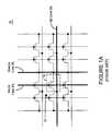
- Another type of dynamic random access memory cell is described and illustrated in non-provisional patent application entitled “Semiconductor Memory Device”, which was filed on Jun. 10, 2003, and assigned Ser. No. 10/450,238 (hereinafter “Semiconductor Memory Device Patent Application”). With reference to
FIGS. 1A and 1B , the Semiconductor Memory Device Patent Application discloses, among other things,semiconductor memory device 10 in which eachmemory cell 12 consists oftransistor 14 havinggate 16,body region 18, which is electrically floating,source region 20 anddrain region 22. Thebody region 18 is disposed between and adjacent tosource region 20 and drainregion 22. Data is written into or read from a selected memory cell by applying suitable control signals to a selected word line(s)24, a selected source line(s)26 and/or a selected bit line(s)28. In response, charge carriers are accumulated in or emitted and/or ejected from electrically floatingbody region 18 wherein the data states are defined by the amount of carriers within electrically floatingbody region 18. Notably, the entire contents of the Semiconductor Memory Device Patent Application, including, for example, the features, attributes, architectures, configurations, materials, techniques and advantages described and illustrated therein, are incorporated by reference herein. - In particular, in one embodiment, the memory cell of the Semiconductor Memory Device Patent Application operates by accumulating in or emitting/ejecting majority carriers (electrons or holes)30 from
body region 18 of, for example, N-channel transistors. (See,FIGS. 2A and 2B ). In this regard, accumulating majority carriers (in this example, “holes”)30 inbody region 18 ofmemory cells 12 via, for example, impact ionization nearsource region 20 and/ordrain region 22, is representative of a logic high or “1” data state. (See,FIG. 2A ). Emitting or ejectingmajority carriers 30 frombody region 18 via, for example, forward biasing the source/body junction and/or the drain/body junction, is representative of a logic low data state (“0 or A0”). (See,FIG. 2B ). - Several techniques may be implemented to read the data stored in (or write the data into) the memory cell. For example, a current sense amplifier may be employed to read the data stored in memory cells. In this regard, a current sense amplifier may compare the cell current to a reference current, for example, the current of a reference cell. From that comparison, it may be determined whether memory cell contained a logic high data state (relatively more majority carriers contained within body region) or logic low data state (relatively less majority carriers contained within body region). The differences of the charge stored in the body of the transistor affects the threshold voltage of the transistor, which in turn affects the current conducted by the transistor when switched into its conductive state.
- In particular, with reference to
FIG. 3 , sense amplifier32 (for example, a cross-coupled sense amplifier) compares the current conducted bytransistor 14 ofmemory cell 12 with a reference current generated by referencecurrent generator 34. The magnitude of the reference current generally lies between the magnitudes of the currents conducted in the logic high data state and logic low data state ofmemory cell 12. Thesense amplifier 32 compares the reference current to the current produced by memory cell12 (the current varies depending on whethermemory cell 12 is either in a logic high data state or logic low data state). Based on that comparison,sense amplifier 32 generates or outputs an output signal (on output36) having a positive or negative polarity, depending upon whethermemory cell 12 stored a logic high or logic low binary data state. - With reference to
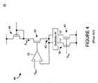
FIG. 4 , a conventional reference current generator includes transistor38, which stores a logic high data state, andtransistor 40, which stores a logic low data state. The referencecurrent generator 34 also includes switches44 (comprised of, for example, transistors) which selectively connecttransistors 38 and40 tonode 42. In addition,switches 44 may selectively isolatetransistors 38 and40 to enable data states to be written intotransistors 38 and40. During a read operation,switches 44 are closed to connecttransistors 38 and40 tonode 42. - With continued reference to
FIG. 4 , referencecurrent generator 34 further includes cascadecurrent source 46 which includesPMOS transistor 48 having its gate connected to its source, in series withNMOS transistor 50, the source of which is connected tonode 42. The gate bias voltage ofNMOS transistor 50 is controlled by connectingnode 42 to the inverting input ofoperational amplifier 52. The output ofoperational amplifier 52 is connected to the gate ofNMOS transistor 50. The non-inverting input ofoperational amplifier 52 is supplied with a reference voltage (VBLR). - The total current passing through node42 (ignoring the negligible input current of operational amplifier52) may be characterized as the sum of the currents passing through
transistors 38 and40, (i.e., the sum of the currents conducted bytransistors 38 and40 having a logic high data state and a logic low data state, respectively). In operation, the current passing throughnode 42 adjusts the voltage ofnode 42, which in turn adjusts the gate-source voltage ofNMOS transistor 50 until the current (2Iref) supplied by cascadecurrent source 46 equals to the sum of the currents flowing throughtransistors 38 and40. - Conventional reference current generators (for example, reference
current generator 34 ofFIGS. 3 and 4 ) tend to “track” changing characteristics ofmemory cell 12, for example, changes induced by temperature variations and/or aging of the transistors, in a relatively slow manner. In addition, referencecurrent generator 34 often has a high noise correlation withmemory cell 12. In this regard, rapid voltage changes (for example, voltage spikes) on the gate, drain, source or silicon on insulator back gate voltage ofmemory cell 12 will also be imposed or replicated ontransistors 38 and40. As such, the difference between the current ofmemory cell 12 and the reference current tend to remain largely unchanged. - However, the reference current generator configuration of
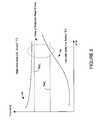
FIGS. 3 and 4 suffers from a drawback that the charge state oftransistors 38 and40 decays over time. (See,FIG. 5 ). As a result, the magnitude of the reference current also changes overtime (for example, decays over time). In this regard, the reference current varies throughout its refreshing cycle between a value “Ref1” at the beginning of a refreshing cycle, and “Ref2” at the end of the cycle. Accordingly, the charge states oftransistors 38 and40 must be periodically refreshed. Notably,transistors 38 and40 should be refreshed at least as often as that ofmemory cell 12 in order to ensure proper operation. - In addition, such a conventional configuration also suffers from the disadvantage that the
transistors 38 and40 may often be at a different stage of refresh cycles relative tomemory cell 12. This is particularly disadvantageous in the case illustrated inFIG. 5 , in whichreference transistors 38 and40 are newly or recently refreshed (i.e., references near the beginning of the cycle, indicated inFIG. 5 as54) andtransistor 14 ofmemory cell 12 is near the end of its cycle prior to refreshing. Under this circumstance, whentransistor 40 provides a current (representative of a decayed data state) that is equal to the reference current (indicated inFIG. 5 as56),sense amplifier 32 may have difficulty, or may no longer be capable of, distinguishing between logic low data state and a logic high data state. In this way, a data reading uncertainty arises. - Notably, in
sense amplifier 32 of the conventional-type, offset currents and/or voltages may arise because of transistor mismatch. Furthermore, the parasitic capacitances of the interconnection traces or wires as well as the storage cells themselves may neither be perfectly matched. These effects limit the accuracy with which the magnitude of the reference signal can be chosen between the magnitude of the signals representing the logic high data state and the logic low data states. This is particularly problematic in integrated memory devices of very small transistor size, even if the memory device consists of generally identical transistors. - There are many inventions described and illustrated herein. In a first principal aspect, the present invention is a semiconductor dynamic random access memory device comprising a plurality of bit lines, including a first bit line and a second bit line, and a first digitally controlled reference current generator, selectively coupled to the first bit line, to generate a first reference current in response to a first reference current control word. The memory device also includes a plurality of memory cells, including a first memory cell coupled to the first bit line and a second memory cell coupled to the second bit line. The memory cells store a first data state and a second data state. Each memory cell includes at least one transistor including a source region, a drain region, a body region disposed between and adjacent to the source region and the drain region and a gate spaced apart from, and capacitively coupled to, the body region. The body region stores a charge such that the transistor includes a first state representative of a first charge in the body region and a second state representative of a second charge in the body region. Notably, the memory cell is in: (1) the first data state when the first transistor is in the first state and (2) the second data state when the first transistor is in the second state.
- The memory device also includes a sense amplifier, having a first input coupled to the first bit line and a second input coupled to the second bit line. The sense amplifier uses the first reference current to sense whether the second memory cell is in the first data state or the second data state.
- In one embodiment, the semiconductor dynamic random access memory device further includes a second digitally controlled reference current generator, selectively coupled to the second bit line, to generate a second reference current in response to a second reference current control word. The sense amplifier uses the second reference current to sense whether the first memory cell is in the first data state or the second data state.
- In another embodiment, the first digitally controlled reference current generator is selectively coupled to the second bit line when the sense amplifier is sensing the data state of the first memory cell. In this regard, the sense amplifier uses the first reference current to sense whether the first memory cell is in the first data state or the second data state.
- The semiconductor dynamic random access memory device may also include a control unit, coupled to the first digitally controlled reference current generator, to generate the reference current control word. The control unit may generate the reference current control word during start-up/initialization and/or during normal operation. In one embodiment, the control unit uses a successive approximation technique to determine the reference current control word. The control unit may be selectively coupled to the sense amplifier to execute the successive approximation technique that determines the reference current control word.
- Notably, the control unit may be coupled to the first and second digitally controlled reference current generators to generate the first reference current control word and the second reference current control word.
- In one embodiment, the second digitally controlled reference current generator generates a reference current in response to the first reference current control word. In this embodiment, the sense amplifier uses the reference current to sense whether the first memory cell is in the first data state or the second data state.
- The semiconductor dynamic random access memory device may include first and second bit lines that are connected to the sense amplifier in an open bit line architecture or a folded bit line architecture.
- In another aspect, the present invention is a semiconductor dynamic random access memory device comprising a plurality of memory cells arranged in a matrix of rows and columns wherein each memory cell includes at least one transistor including a source region, a drain region, a body region disposed between and adjacent to the source region and the drain region, wherein the body region is electrically floating, and a gate spaced apart from, and capacitively coupled to, the body region. The transistor includes a first state representative of a first charge in the body region and a second state representative of a second charge in the body region. The memory cell is in: (1) the first data state when the first transistor is in the first state and (2) the second data state when the first transistor is in the second state.
- The semiconductor dynamic random access memory device of this aspect further includes a plurality of bit lines, including a first bit line connected to a first memory cell and a second bit line connected to a second memory cell, and a plurality of digitally controlled reference current generators. Each digitally controlled reference current generator being selectively coupled to an associated one of the bit lines to provide a reference current in response to an associated reference current control word. A plurality of sense amplifiers senses: (1) the data state of the memory cells connected to a first associated bit line using the reference current provided by a digitally controlled reference current generator connected to a second associated bit line, and (2) the data state of the memory cells connected to a second associated bit line using the reference current provided by a digitally controlled reference current generator connected to a first associated bit line.
- In one embodiment of this aspect of the invention, the semiconductor dynamic random access memory device includes a control unit, coupled to the first digitally controlled reference current generator, to generate the reference current control word for each reference current generator. In one embodiment, the control unit uses a successive approximation technique to determine the reference current control word for at least one reference current generator. The control unit may be selectively coupled to the sense amplifier associated with the at least one reference current generator to execute the successive approximation technique that determines the reference current control word.
- The reference current control words may be provided to the reference current generators during an initialization sequence. The reference current control words may also provided to the reference current generators during normal operation. In one embodiment, the control unit may generate the reference current control words during normal operation of the memory device, and wherein the reference current control words are provided to the reference current generators during normal operation.
- The bit line layout of the semiconductor dynamic random access memory device of this aspect of the invention may include an open bit line architecture or a folded bit line architecture.
- In yet another aspect, the present invention is a semiconductor dynamic random access memory device comprising a plurality of bit lines, including first and second bit lines and a sense amplifier, having a first input coupled to the first bit line and a second input coupled to the second bit line. The memory device may also include a first reference current generator, selectively coupled to the first bit line, to generate a first reference current in response to a reference current control word, and a second reference current, selectively coupled to the second bit line, to generate a second reference current in response to the reference current control word.
- In addition, the memory device may also include a plurality of memory cells, including a first memory cell coupled to the first bit line and a second memory cell coupled to the second bit line, wherein the memory cells each store a first data state and a second data state. Each memory cell may include at least one transistor including a source region, a drain region, a body region disposed between and adjacent to the source region and the drain region, wherein the body region is electrically floating, and a gate spaced apart from, and capacitively coupled to, the body region. The transistor includes a first state representative of a first charge in the body region and a second state representative of a second charge in the body region. The memory cell is in: (1) the first data state when the first transistor is in the first state and (2) the second data state when the first transistor is in the second state.
- In operation, the sense amplifier uses: (1) the first reference current to sense whether the second memory cell is in the first data state or the second data state, and (2) the second reference current to sense whether the first memory cell is in the first data state or the second data state.
- In one embodiment, the semiconductor dynamic random access memory device includes a control unit, coupled to the first reference current generator, to adjust the first reference current generated by the first reference current generator. The control unit may employ a successive approximation technique to determine the reference current control word. Notably, the control unit may selectively couple to the sense amplifier to execute the successive approximation technique that determines the reference current control word.
- In one embodiment, the first and second reference current generators are digitally controlled reference current generators. In another embodiment, the first and second reference current generators are analog reference current generators.
- The control unit may generate the first reference current control word during an initialization sequence of the memory device. The control unit may also generate the first reference current control word during normal operation of the memory device.
- The bit line layout of the semiconductor dynamic random access memory device of this aspect of the invention may include an open bit line architecture or a folded bit line architecture.
- Again, there are many inventions described and illustrated herein. This Summary of the Invention is not exhaustive of the scope of the present invention. Moreover, this Summary is not intended to be limiting of the invention and should not be interpreted in that manner. While certain embodiments, features, attributes and advantages of the inventions have been described in this Summary, it should be understood that many others, as well as different and/or similar embodiments, features, attributes and/or advantages of the present inventions, which are apparent from the description, illustrations and claims, which follow.
- In the course of the detailed description to follow, reference will be made to the attached drawings. These drawings show different aspects of the present invention and, where appropriate, reference numerals illustrating like structures, components, materials and/or elements in different figures are labeled similarly. It is understood that various combinations of the structures, components, materials and/or elements, other than those specifically shown, are contemplated and are within the scope of the present invention.
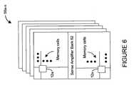
FIG. 1A is a schematic representation of a portion of a DRAM array as illustrated (and described) in the Semiconductor Memory Device Patent Application;FIG. 1B illustrates a memory cell according to the Semiconductor Memory Device Patent Application;FIGS. 2A and 2B are exemplary schematic illustrations of the charge relationship, for a particular memory state, of the floating body, source and drain regions of a memory cell according to the Semiconductor Memory Device Patent Application;FIG. 3 is a block-diagram illustration of a conventional circuit configuration to read data from a memory cell;FIG. 4 is a schematic representation of a conventional reference current generating circuit, which may be implemented in the configuration ofFIG. 3 ;FIG. 5 is a graphical illustration of the variation of current with time of the data storage cell and reference current generator of theFIGS. 3 and 4 ;FIG. 6 is a block diagram representation of a memory device including a plurality of memory cells at the intersection of rows and columns of a plurality of memory arrays;FIG. 7 is a schematic representation of a portion of a memory device, including a reference current generator and circuitry to control and/or set the reference current generator, in accordance with a first aspect of the present invention;FIGS. 8-10 are schematic representations of several embodiments of a reference current generator that are suitable for use in the portion of a memory device illustrated inFIG. 7 ;FIGS. 11A and 11B are exemplary schematic representations of suitable reference current generators according to a second aspect of the present invention;FIGS. 12A-12C are schematic block diagrams of certain embodiments of the digitally controlled reference current generator according to the second aspect of the present invention;FIG. 13A is a schematic representation of a portion of a memory device, including a sense amplifier and two bit lines having a plurality of memory cells attached thereto, in accordance with an embodiment of the present invention;FIG. 13B is a schematic representation of a portion of a memory device, including a control unit, a sense amplifier and two bit lines having a plurality of memory cells attached thereto, in accordance with another embodiment of the present invention;FIG. 14A is a detailed schematic representation of a sense amplifier in accordance with an embodiment of the present invention; andFIG. 14B is a detailed schematic representation of a sense amplifier, in conjunction with a control unit, in accordance with another embodiment of the present invention;FIG. 15 is a flow diagram of an exemplary successive approximation technique for determining the reference current control word according to certain embodiments of the present invention;FIG. 16A is a schematic representation of a portion of a memory device, including a sense amplifier and one reference current generator, in accordance with an embodiment of the present invention; andFIG. 16B is a schematic representation of a portion of a memory device, including a control unit, a sense amplifier and one reference current generator, in accordance with another embodiment of the present invention.- There are many inventions described and illustrated herein. In a first aspect, the present invention is a technique and circuitry for reading data that is stored in memory cells. In one embodiment of this aspect, the present invention is a technique and circuitry for generating a reference current that is used, in conjunction with a sense amplifier, to read data that is stored in memory cells of a memory device (for example, a DRAM device). The technique and circuitry for generating a reference current may be implemented using an analog configuration, a digital configuration, and/or combinations of analog and digital configurations.
- In one embodiment, the memory cells include one or more transistors, each having an electrically floating body in which an electrical charge is stored. In this regard, the memory cells may be comprised of one transistor which stores an electrical charge in the body region which is representative of a binary state (see, for example,
FIGS. 1A, 1B ,2A and2B). Notably, the transistor that comprises the memory cell may employ any type of design and/or control technique, whether now known or later developed, including, for example, those discussed above in the Semiconductor Memory Device Patent Application as well as those discussed in “Semiconductor Memory Device and Method of Operating Same”, which was filed on May 6, 2004, by Ferrant, Okhonin, Carman and Bron, (hereinafter “Semiconductor Memory Device Patent Application II”). The entire contents of the Semiconductor Memory Device Patent Application II, including, for example, the features, attributes, architectures, configurations, materials, techniques and advantages described and illustrated therein, are incorporated by reference herein. - In another embodiment, the memory cells may be comprised of more than one transistor. For example, the memory cells may include two transistors, which are arranged and/or configured as a complementary memory cell that is read and/or determined by sampling, sensing, measuring and/or detecting the polarity of the logic states stored in each transistor of complementary memory cell. That is, the two-transistor complementary memory cell is read by sampling, sensing, measuring and/or detecting the difference in signals (current or voltage) stored in the two transistors. (See, for example, the memory cell, architectures, layouts and/or configurations described and illustrated in “Semiconductor Memory Cell, Array, Architecture and Device, and Method of Operating Same”, which was filed on Apr. 22, 2004 and assigned Ser. No. 10/829,877 (hereinafter “Semiconductor Memory Cell Patent Application”). Notably, the entire contents of the Semiconductor Memory Cell Patent Application, including, for example, the features, attributes, architectures, layouts, configurations, materials, techniques and advantages described and illustrated therein, are incorporated by reference herein.
- Indeed, the memory cells may be arranged and/or configured in an array, and controlled (written to, read from and/or refreshed) in many, many different ways. All such arrangements, layouts, designs and/or control techniques for the memory cells described above, whether now known or later developed, are intended to be within the present invention. For example, the memory cells may be arranged and/or configured in arrays as described in Semiconductor Memory Device Patent Application II and/or Semiconductor Memory Cell Patent Application. The memory cells may be controlled in the manner described in those patent applications. Again, the features, attributes, architectures, layouts, configurations, materials, techniques and advantages described and illustrated in Semiconductor Memory Device Patent Application II and/or Semiconductor Memory Cell Patent Application are incorporated by reference herein and may be implemented in conjunction with the inventions described in this application. For the sake of brevity, those discussions will not be repeated.
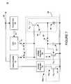
- With reference to
FIGS. 1A, 6 and7,memory device 10 includes one or more memory arrays58a-nofmemory cells 12a-x(for example, one or more partially depleted SOI (PD SOI)type transistors 14 forming individual memory cells12). The transistor(s)14 ofmemory cell 12 may be a symmetrical or non-symmetrical device(s). Where transistor(s)14 is/are symmetrical, the source and drain regions are essentially interchangeable. However, where transistor(s)14 is/are non-symmetrical device(s), the source or drain regions of transistor(s)14 have different electrical, physical, doping concentration and/or doping profile characteristics. As such, the source or drain regions of a non-symmetrical device are typically not interchangeable. - In one embodiment,
memory device 10 determines the binary logic state stored in a givenmemory cell 12 using referencecurrent generator 60 and sense amplifier32 (for example, a cross-coupled sense amplifier as illustrated inFIG. 14 ), which is one of a plurality of sense amplifier ofsense amplifier bank 62. In particular, in one embodiment, the binary logic state of data stored bymemory cell 12a(one of the plurality of memory cells contained in memory array58a-n) is sensed bycoupling memory cell 12atosense amplifier 32 via, for example,voltage regulator 64. Thesense amplifier 32 receives the current conducted bymemory cell 12aand compares that current to a reference current generated by referencecurrent generator 60. In response,sense amplifier 32 generates one or more output signals (for example, on output signal line66) that is/are representative of the data stored in thememory cell 12a. That is, the output ofsense amplifier 32 will be either high or low (for example, positive or negative) depending upon the charge state ofmemory cell 12. - The magnitude of the reference current produced by reference
current generator 60 is generally between (i) the magnitude of the current conducted bymemory cells 12 when storing a logic high data state and (ii) the magnitude of the current conducted bymemory cells 12 when storing a logic low data state. The circuitry and techniques for controlling referencecurrent generator 60 employ the output(s) ofsense amplifier 32 to control, calibrate and/or set the magnitude of the reference current produced by referencecurrent generator 60. In this regard, the output(s) ofsense amplifier 32 are input to controlunit 68, which outputscontrol signal 70 to referencecurrent generator 60. Notably,control signal 70 may consist of a plurality of bits (the reference current control word) that are converted to an analog representation (signal74), via digital-to-analog converter (DAC)72, and selectively applied to referencecurrent generator 60 using switch76 (for example, a transistor). - The reference
current generator 60 includestransistor 78 connected viavoltage regulator 80 and switch82 (for example, a transistor) tosense amplifier 32. The referencecurrent generator 60 may also includelevel shifter 84 to control the operating and/or responsive characteristics oftransistor 78. Thelevel shifter 84 includestransistor 86 connected in series withcurrent source 88. The gate oftransistor 86 is connected to senseamplifier 32 viaswitch 82, and toDAC 72 viaswitch 76. The source oftransistor 86 is connected to the body oftransistor 78 via switch90 (for example, a transistor). Thecapacitor 92 is connected between the body and source oftransistor 78 to hold any voltage signal applied bytransistor 86 viaswitch 90. - With reference to
FIG. 8 , referencecurrent generator 60 is shown in more detail. Thevoltage regulator 80, in one embodiment, may be comprised oftransistor 94 and operational amplifier96 (for example, a voltage-to-voltage amplifier or voltage-to-current amplifier). The source oftransistor 94, in this embodiment, is connected to the drain oftransistor 78. Further, the gate oftransistor 94 is connected to the output ofoperational amplifier 96. A reference voltage VBLRis applied to the non-inverting input ofoperational amplifier 96, and the inverting input is connected to the junction of the source oftransistor 94 and the drain oftransistor 78. - With reference to
FIGS. 5-8 , in operation,transistor 78, when switched into its conductive state by a word line voltage VWLapplied to its gate, such that the gate-source voltage oftransistor 78 exceeds the threshold voltage, conducts a drain current determined by the difference between gate voltage VWLand the threshold voltage oftransistor 78. Current is supplied to the channel oftransistor 78 bytransistor 94, and the voltage atpoint 98 at the junction of the source oftransistor 94 and the drain oftransistor 78 settles at a value at whichtransistor 94, controlled byoperational amplifier 96, conducts a current appropriate to the data state oftransistor 78. - The
switch 90 is open during normal operation and is closed at, for example, regular and/or periodic intervals. Whenswitch 90 is closed, the voltage at the source oftransistor 86charges capacitor 92 and is applied to the substrate oftransistor 78. In this way, the threshold voltage oftransistor 78 changes (due to the charging of the substrate of transistor78), and the current conducted bytransistor 78 for a given gate to source voltage also changes. - As the charge in the body of
transistor 78 decays with time, the high data state current decreases slightly, and the low data state current increases to a greater extent than the high data state current. As the current conducted by transistor78 (and therefore the current conducted by transistor94) increases, the voltage at the drain oftransistor 94 increases, as a result of which the source voltage oftransistor 86 is also caused to increase. This increases the voltage at the substrate oftransistor 78, as a result of which the threshold voltage oftransistor 78 increases. By increasing the threshold voltage oftransistor 78, the drain current oftransistor 78 decreases, as a result of which the reference current generated bytransistor 78 is maintained generally constant despite decay, over time, of the current provided or sunk bytransistor 78. - The value of the reference current may be set by applying a high data state to all of
memory cells 12, and reading the output of one ormore memory cells 12. Under these conditions, switch76 is closed, and control unit68 (via signal70) iteratively or repeatedly adjusts the value of reference current provided by referencecurrent generator 60. In one embodiment, the reference current is iteratively or repeatedly adjusted and/or set to a value that is slightly lower than the lowest value of the high data state current formemory cells 12. Thecontrol unit 68 implements a reference current algorithm to control and/or set the reference current output by referencecurrent generator 60. - Briefly, the reference current adjustment algorithm, in certain embodiments of the present invention, adjustments, compensates and/or sets the reference current to a value that provides an optimum, enhanced and/or predetermined read window (via optimum, enhanced and/or predetermined values of the reference current output by reference current generator60). The reference current adjustment algorithm may implement an iterative process to determine the optimum, enhanced and/or predetermined read window. That is, the “initial” or existing reference current output by reference
current generator 60 may be applied, andcontrol unit 68 may determine the output ofsense amplifier 32 in view of a known (predetermined) state ofmemory cell 12. In response to that determination, the reference current may be adjusted based on the result from sense amplifier32 (i.e., is the reference current or the sensing operation within, above or below a desired, selected and/or predetermined range of results). - Thereafter,
control unit 68 may again set referencecurrent generator 60 to provide a slightly increased or decreased reference current. After sensing the known (predetermined) state ofmemory cell 12 viasense amplifier 32, additional adjustment and/or compensation of the output of referencecurrent generator 60 may be implemented, viacontrol unit 68, as required in view of the result from sense amplifier32 (i.e., is the reference current or the sensing operation within, above or below a desired, selected and/or predetermined range of results). Based on that determination, the process is either repeated or terminated. - The iterative process may be implemented in a “degrading” manner or “improving” manner. That is, the initial or existing reference current output by reference
current generator 60 may be initially configured outside the acceptable limits and incrementally improved until within the acceptable limit (i.e., a limit that provides a correct sense operation which may or may not include a margin). Alternatively, or in addition, the “initial” or existing reference current output by referencecurrent generator 60 may be initially configured within the acceptable limits (i.e., a limit that provides a correct sense operation which may or may not include a margin) and incrementally degraded until outside the acceptable limit. In this way,control unit 68 may then set and/or configure referencecurrent generator 60 to provide an appropriate reference current. - Thereafter, switch76 may be opened (and the programming and/or control of reference
current generator 60 terminated) andmemory cells 12 may be programmed with data of unknown, desired, predetermined and/or selected states. The data state ofmemory cells 12 may be read by comparing the current conducted by a givenmemory cell 12awith the reference current (generated by reference current generator60) insense amplifier 32 and the result output as output signals on signal line(s)66. - The performance of the sensing operation (for example, the performance of the circuitry of
FIG. 7 ) may be measured, determined, inspected, characterized and/or evaluated, intermittently, periodically, during device initialization, re-initialization and/or at start-up or power-up, and/or in situ (for example, during device evaluation/inspection/test, during device initialization, re-initialization and/or at start-up or power-up). In this way, the performance ofmemory device 10 may be periodically and/or intermittently measured, inspected, characterized, determined and/or evaluated to, for example, (1) ensure that the reference current generator and/or the sensing operation is/are operating properly, and/or (2) ensure that the reference current generator and/or the sensing operation is/are within acceptable operating parameters. - The
control unit 68 may implement the setting, calibration and/or tuning techniques for one, some or all of referencecurrent generators 60 withinmemory device 10. In this regard, the control signal provided toDAC 72 may be determined for one, some or all of referencecurrent generators 60 and, as such,control unit 68 programs or re-programs one, some or all referencecurrent generators 60. Thecontrol unit 68 may set, calibrate and/or tune one, some or all of referencecurrent generators 60 as described immediately above. In those embodiments where a plurality of referencecurrent generators 60 are set, calibrated and/or tuned, switch76 may be a multiplexer having an input coupled toDAC 72 and a plurality of outputs, each coupled to one or more referencecurrent generators 60. - In addition, the reference current provided by reference
current generators 60 may be periodically and/or intermittently “refreshed” in order to provide an enhanced, optimum, desired, predetermined and/or “minimum” reference current. In this regard, in one embodiment,control unit 68 may periodically and/or intermittently connectDAC 72, via switch76 (or a multiplexer), to one or more referencecurrent generators 60. TheDAC 72 provides an analog representation of the reference current control word (for example, the previously determined reference current control word) to referencecurrent generator 60 usingswitch 76. In this way, in the event that the reference current provided by one or more referencecurrent generators 60 may not be (currently or impending) providing an enhanced, optimum, desired, predetermined and/or “minimum” reference current, for example, after a predetermined or given period of time (during operation or after setting, calibration and/or tuning), thecontrol unit 68 “refreshes” those referencecurrent generators 60. - With reference to
FIG. 9 , since it may be difficult in practice to enable the substrate oftransistor 78 ofFIGS. 7 and 8 to match the behavior of a PD SOI transistor used asmemory cell 12, (for example, because the PD SOI transistor has no body contact whiletransistor 78 includes a substrate contact),level shifter 84 applies a voltage signal to the gate oftransistor 78 to whichauxiliary capacitor 100 is connected in series. The gate voltage oftransistor 78 approximately simulates substrate charges found in the PD SOI transistors ofmemory cells 12, provided the capacitance ofauxiliary capacitor 100 is sufficiently large that the gate voltage oftransistor 78 almost equals the external voltage VWL. - Notably, reference
current generator 60 need not include level shifter84 (see,FIG. 10 ). Where no level shifter is employed, the drain voltage oftransistor 94 may be applied directly to the gate oftransistor 78. (See, in addition, the circuitry illustrated inFIGS. 8 and 9 as well). However, in those embodiments where a level shifter is employed, the level shifter may be implemented using any number of techniques, for example, via a resistive divider and/or an operational amplifier(s). As such, any design and/or configuration of the level shifter, whether now known or later developed, is intended to come within the scope of the present invention. - In another aspect of the present invention, the reference current generator may be implemented using a more digital circuit approach. With reference to
FIG. 11A and 12A , in one embodiment, referencecurrent generator 102 includes a plurality of transistors104a-nand106a-n, andcurrent source 108 arranged in a current mirror configuration. The plurality of transistors104a-nand106a-n, in combination, function as a variable resistor. In this regard, first plurality of transistors104a-nis selectively controlled, using a reference current control word (including 2, 3, 4, 5 or more bits), to incorporate associated transistor106a-ninto the current path. The second plurality of transistors106a-nincludes the same or different conductance characteristics to provide or produce an adjustable and/or controllable current. In this regard, in one embodiment, for example,transistor 106amay have a conductance ratio, relative totransistor 106b, of half. As such, in this embodiment,transistor 106aconducts ½ the current relative totransistor 106b. Notably, the transistor conductance ratios may be implemented by selectively designing and controlling the relative widths of transistors106. - It should be further noted that the ratios and/or weighting of the transistor may be determined and/or established to provide a predetermined, enhanced and/or optimum flexibility using the fewest transistors. Indeed, any and all weighting and/or ratios, whether now known or later developed, are intended to come within the scope of the present invention.
- With reference to
FIG. 11B , in another example, referencecurrent generator 102 may be implemented as a MOS ladder DAC. For example,FIG. 11B illustrates an exemplary n-bit M2M ladder DAC where a full scale is imposed by the current source (Isource). The referencecurrent generator 102 uses the reference current control word (Anto A0) to output a suitable, predetermined, selected, optimum and/or enhanced reference current. The current source supplies the DAC reference current and the biasing current (Ip) through the current mirror M1, M2 and M3. Since Iref,max=2(Ip), the current source (Isource) may be used to drive the current mirror with matched transistors (M1, M2, M3) to provide the reference current for the DAC and the biasing current (Ip). - Notably, any digital to analog reference current generator may be implemented as reference
current generator 102, whether now known or later developed. All such digital to analog reference current generators are intended to fall within the scope of the present invention. - The reference current control word may be fixed and/or predetermined. (see, for example,
FIG. 12A ). For example, in one embodiment, the reference current control word may be provided to referencecurrent generator 102 at start-up/power-up and/or during an initialization sequence. In this embodiment, the reference current control word may be determined via a particular configuration of the state of a certain pin or pins on the package ofdevice 10. Alternatively, the fixed or predetermined, preset or pre-programmed reference current control word may be permanently, semi-permanently or temporarily (i.e., until re-programmed) by way of a register (for example, a plurality of DRAM, SRAM, ROM, PROM, EPROM, EEPROM cells that are resident onmemory device 10 or off-chip (for example, disposed on a memory card on whichmemory device 10 resides). - In another embodiment, with reference to
FIGS. 12B and 12C , the reference current control word may be programmable viacontrol unit 110. In this embodiment, an “initial” reference current control word may be provided at start-up/power-up and/or during an initialization sequence. Thereafter, the reference current control word may be re-programmed, viacontrol unit 110, during operation to optimize, enhance, compensate and/or adjust the reference current (provided by reference current generator102). For example, the reference current may be adjusted during operation ofmemory device 10 to address and/or compensate for variations in operating conditions (for example, to compensate for changes in temperature or response time parameters or characteristics). - Further, yet another embodiment, the reference current control word may be fine-tuned to enhance the performance of
memory device 10. In this regard, after (or during) the performance of an initialization or re-initialization process,memory device 10 may implement fine adjustments to the predetermined, preset or pre-programmed reference current control word. The adjustments to the reference current control word may be accomplished using any techniques. Notably, all techniques for determining the reference current control word, whether now known or later developed, are intended to be within the scope of the present invention. - For example, in those embodiments where
control unit 110 programs or re-programs one, some or all referencecurrent generators 102,control unit 110 may implement a successive approximation approach to determine a reference current control word that, in conjunction with referencecurrent generator 102, provides an optimized, enhanced, compensated and/or adjusted reference current. In this embodiment,control unit 110 may store the reference current control word in successive approximation registers112aand112b(see, for example,FIG. 12C ). - With reference to
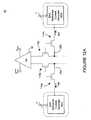
FIG. 13 , in one embodiment,memory device 10 includessense amplifier 32, one input of which is connected tofirst bit line 28aand the other input of which is connected tosecond bit line 28b. A plurality ofmemory cells 12a1, to12am(for example, the one PD SOI transistor configuration) are connected to bitline 28a. The referencecurrent generator 102ais also connected to bitline 28a(viatransistor 114a), which is in turn connected to an input node ofsense amplifier 32. Notably,bit line 28ais selectively connected to senseamplifier 32 viatransistor 116a. - Similarly,
bit line 28bis generally identical tobit line 28aand is connected to an input node ofsense amplifier 32. A plurality of memory cells12b1to12bm(for example, the one PD SOI transistor configuration) are connected to bitline 28b. The referencecurrent generator 102bis also connected to thebit line 28b(viatransistor 114b), which is in turn connected to an input node ofsense amplifier 32. - The reference
current generator 102aselectively provides a reference current tosense amplifier 32 in those instances wheresense amplifier 32 senses the data state of a memory cell12b1, to12bmdisposed onbit line 28b. In contrast, referencecurrent generator 102bselectively provides a reference current tosense amplifier 32 in those instances wheresense amplifier 32 is configured to sense the data state of amemory cell 12a1to12amdisposed onbit line 28a. - Notably, reference
current generators current generators control unit 110 may dependently or independently adjust, program and/or control referencecurrent generators FIG. 13B ). - With reference to
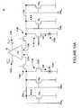
FIGS. 14A and 14B , in one embodiment,sense amplifier 32 includes a pair ofcross-coupled CMOS inverters inverter 118aincludesNMOS transistor 120, having its source connected to inputnode 122aand to the drain ofNMOS transistor 124. Theinverter 118aalso includesPMOS transistor 126. Notably, the drains oftransistors output node 128a(i.e., Vout\). - Similarly,
CMOS inverter 118bincludesNMOS transistor 130, having its source connected to inputnode 122band to the drain oftransistor 132. Theinverter 118balso includesPMOS transistor 134. The drains oftransistors output node 128b. The gates oftransistors output node 128a, while the gates oftransistors output node 128b. Further, the gates oftransistors transistor 136, which functions as a switch, andinput nodes transistor 138, which also functions as a switch. - In addition,
sense amplifier 32 is selectively connected to voltage rail VSAPviatransistor 140. The gates oftransistors transistors voltage regulator 80 ofFIGS. 8 and 9 serves the same purpose - Notably, in the embodiment of
FIG. 14B ,output nodes control unit 110 during the programming, calibration and/or adjustment process of referencecurrent generators 102aand/or102b. - With reference to
FIGS. 13A, 13B ,14A and14B, in operation, the presence or absence of a net positive charge in the body of a transistor ofmemory cell 12 represents one of a binary logic states. As mentioned above, the threshold voltage of the transistor ofmemory cell 12 is dependent upon the charge storage state of the transistor. As a result, when a suitable gate-source voltage is applied to the transistor ofmemory cell 12, a source-drain current is conducted, the magnitude of which depends upon the threshold voltage of the transistor, which in turn depends upon its charge state. Accordingly, the logic state of the bit of data stored inmemory cell 12 may be determined by comparison of the current conducted by the respective transistor with a reference current value. - It is found that the logic high data state and the logic low data state of the PD SOI transistors forming
memory cells 12 approach each other with time (the charge within the electrically floating body region decays over time), but the logic high data state decays more slowly than the logic low data state. As such, it may be advantageous to set the magnitude of the reference current between the logic high and logic low data states, but closer to the more slowly varying logic high data state. In this way, the validity of the reference current magnitude for as long as possible between data refreshing operations may be ensured. - In one embodiment, the magnitude of the reference current produced by reference
current generator 102a, a logic high data state is initially written to one or more (preferably all) of memory cells12b1to12bm, which are connected to bitline 28b. This may be accomplished by applying a suitable voltage to signalbit line 28b, and suitable voltage signals to word lines24b1, to24bm. At this stage,bit lines sense amplifier 32 by turning offtransistors sense amplifier 32 is disabled by turning offtransistor 140 and turning ontransistors 136. In this way,sense amplifier 32 consumes little to no power. - The binary logic state of the data stored in
memory cell 12 may be read by initiating a precharge phase of the reading operation. In this regard,transistor 140 is turned on, providing power tosense amplifier 32. The voltage rail value VSAPmay be reduced in order to properly adjust the switching point(s) ofinverters transistor 138 may be enabled or turned-on in order to equalize or balance the inputs ofsense amplifier 32. In addition,transistors bit lines sense amplifier 32. The other voltage rail value VCLAMPmay be brought to the reading voltage. - Notably,
transistor 136 is also switched on to force equal voltages ontooutput nodes sense amplifier 32. The voltage atoutput nodes transistors - At the end of the precharge phase, the operation to read the data logic state of transistor(s) of
memory cell 12ambegins by switching offtransistor 138, and setting the reading voltage on word lines24amto cause the corresponding transistor(s) ofmemory cell 12amto conduct a current. At the same time, referencecurrent generator 102bis connected to bitline 28b(andinput node 122bofsense amplifier 32 by turning ontransistor 114b. At this moment,memory cell 12amand referencecurrent generator 102bstart discharging the parasitic capacitances of both bitlines input nodes sense amplifier 32. - Notably, reference
current generator 102ais disconnected frombit line 28aby maintainingtransistor 114ain an off state. Indeed, referencecurrent generator 102ais employed to only read memory cells connected to bitline 28b. - After completion of the sense portion of the reading operation, a restore portion of the reading operation may then be commenced by switching off
transistor 136, reducing VCLAMPto Vss(a low voltage, preferably ground), and possibly increasing VSAPto Vddin order to obtain proper logic levels atoutput nodes inputs nodes sense amplifier 32, the source currents oftransistors output nodes sense amplifier 32. This voltage difference is rapidly amplified by cross-coupled latches formed byinverters output nodes sense amplifier 32 is then input to controlunit 110, where it is processed to generate a reference current control word, which controls referencecurrent generators - In those embodiment where
memory device 10 includescontrol unit 110 to adjust, control and/or program referencecurrent generator 102,control unit 110 may implement a successive approximation algorithm to determine a reference current control word to provide to referencecurrent generator 102 in order to generate a predetermined, desired, enhanced and/or optimum reference current. As mentioned above, the successive approximation algorithm is exemplary, and all techniques and/or algorithms for determining the reference current control word, whether now known or later developed, are intended to be within the scope of the present invention. - In one embodiment, an
exemplary algorithm 142 ofFIG. 15 may be implemented and/or executed at power up (i.e., before using the memory device), and/or intermittently or periodically during normal operation to compensate for, for example, drift due to temperature variations. Briefly, an intention ofexemplary algorithm 142 is to determine the largest “valid” value for the reference current. In this way, the current output bymemory cells 12 that corresponds to logic low data state increases with time, while it remains substantially constant relatively to logic high data state. Notably, althoughexemplary algorithm 142 is suited for this application, other algorithms are suitable for determining an appropriate value (or an optimal value based on other criteria or criterion). Furthermore,exemplary algorithm 142 assumes that the current frommemory cells 12 which corresponds to logic low data state (AO) and logic high data state (Al) provides a suitable read window to permit a valid reference current value to be identified and/or determined. - First,
memory cells 12 that are associated with a particular reference current generator102 (for example, memory cells12b1, to12bmare associated with referencecurrent generator 102a) are programmed to a logic high data state (indicated as142A). The current and/or predetermined value of the magnitude of reference current (IREFSTORE) output by referencecurrent generator 102, which is representative of reference current control word that may be maintained incontrol unit 110, is reset at142B. Notably, this process may be performed for one, some or all memory cells associated with referencecurrent generator 102. In those instances where the algorithm is to be performed for one, some or all memory cells that are associated with a given referencecurrent generator 102, this instruction is provided at142C. - With continued reference to
FIG. 15 , thereafter, the reference current value (IREF) of referencecurrent generator 102ais then set to a known value (for example, zero) at142D, and an incremental value (IREFTRY) of reference current is set at half of a nominal maximum value (IREFMAX) of the reference current (see,142E). The maximum value (IREFMAX) may be determined or estimated empirically (for example, via simulation or testing of a circuit on silicon), and/or chosen arbitrarily. - The reference current may then be increased by incremental value (IREFTRY) at142F and the state of a first memory cell12 (for example, memory cells12b1to12bm) is read by sense amplifier32 (see,142G). Since it is known that all of associated memory cells were initially programmed with a logic high data state (Al),
control unit 110 determines, at142H, whether the output ofsense amplifier 32 is correct. If the output ofsense amplifier 32 is correct, the reference current is less than or equal to the largest valid value for the reference. Notably, at this point it may not be possible to know (with certainty) whether the reference current is too small or if it is large enough to produce a correct output for a logic low data state (A0) as well. - However, since
algorithm 142 is determining the largest valid value for the reference current, and the last tested reference value produced a correct determination (i.e.,sense amplifier 32 sensed a logic high data state (A1)), the value of the reference current (IREF) is maintained unchanged, and the incremental value (IREFTRY) is halved (see,142J and142K). Thecontrol unit 110 may then determine whether the incremental value (IREFTRY) is smaller than a predetermined limiting value of delta (Δ) at142L, and if the limiting value has not been reached, the process returns to142F. - Notably, the delta (Δ) corresponds to the precision of the reference current adjustment. It may be advantageous to be small enough with respect to the separation of the respective current values of
memory cells 12 corresponding to the two data states (“A1” and “A0”). In this way,algorithm 142 may provide a reference current value (or reference current control word) that also produces valid output for logic low data state (“A0”). - However, if it is determined that
sense amplifier 32 has provided an incorrect output, the reference current must be too large (see,142M), and therefore cannot be used to distinguish between the binary data states (“A1” and “A0”). Accordingly, IREFis reduced to its previous value andcontrol unit 110 implements142K. - When the incremental value (IREFTRY) is determined to be less than delta (Δ) at142L, the stored value of the magnitude of reference current (IREFSTORE) is set as the minimum value of the reference current (IREF) determined by
control unit 110 for aparticular memory cell 12 at142N. Notably, the value of the magnitude of reference current (IREFSTORE) may be the largest acceptable value for the reference current for all the memory cells that were “examined”. - The process may be repeated for one, some or all of
memory cells 12 onbit line 128b. In this regard, at142P,control unit 110 determines whether thepervious memory cell 12 under examination is thelast memory cell 12 to be examined. If not, thenext memory cell 12 is connected to bitline 28b, at142Q, and the process returns to142D. Ifcontrol unit 110 determines that theprevious memory cell 12 is the last cell to be examined, the magnitude of reference current (IREF) generated by referencecurrent generator 102ais set to the stored minimum reference value (IREFSTORE) at142R. In this way, a reference current value is set which may be the largest suitable value for the data states (“A1” and “A0”) of allmemory cell 12 connected to bitline 28b. Thememory cells 12 may then be reprogrammed with unknown data states or previous data states subsequently determined by comparing their output currents with the reference current set in referencecurrent generator 102bbysense amplifier 32. - Notably,
control unit 110 may perform or execute the same or similar process for all referencecurrent generator 102 connected toother bit lines 28 in memory device10 (for example,current generator 102b). In this way, each of referencecurrent generators 102 is suitably programmed. - An algorithm may also be employed to determine an appropriate, optimum and/or enhanced reference current when
memory cells 12 that are associated with a particular referencecurrent generator 102 are programmed to a logic low data state. Indeed,control unit 110 may also execute an algorithm when thememory cells 12 are sequentially programmed to a logic high data state and a logic low data state. Thecontrol unit 68 may then determine the most appropriate reference current in the event a different reference current is determined for a logic high data state and a logic low data state (for example, an average of the reference currents). - It may be advantageous to determine an appropriate, optimum and/or enhanced reference current to be output or provided by less than all of reference
current generators 102 and provide the reference current control word that is representative of the appropriate, optimum and/or enhanced reference current to other referencecurrent generators 102. For example, an appropriate reference current control word may be determined for referencecurrent generator 102aand provided to both referencecurrent generators current generators 102 that are associated with a given sense amplifier32). In this regard, referencecurrent generators memory cells 12 disposed onbit lines device 10. In this way, essentially one half of the calibration and/or adjustment routine for referencecurrent generators 102 are eliminated. - Moreover, in another embodiment, a reference current control word may be determined for some or all of reference
current generators 102 using, for example, any of the techniques described herein, and thereafter intermittently and/or periodically “tuned” or “tweaked” to account or compensate for changes in the performance of device10 (for example, changes due to changes in temperature). As such, in this embodiment, at start-up, initialization or re-initialization,control unit 110 may determine a reference current control word (that, in conjunction with referencecurrent generator 102 provides a suitable, predetermined, optimum and/or enhanced reference current) and program referencecurrent generator 102, as described above. Thereafter, the reference current may be adjusted during operation ofmemory device 10 by determining a relative adjustment to the “initial” reference current control word (determined during, for example, at start-up/power-up and/or an initialization sequence). - The relative adjustment(s) may be determined, in any manner described herein, by examining one or some representative reference current generator(s)102 (for example, one or more reference current generator(s)102 in an array and/or memory or sense bank). After determining the relative adjustment(s),
control unit 110 may implement the change to the reference current control word for all reference current generator(s)102 (even those reference current generator(s)102 that have not be directly “analyzed” by the control unit110). In this way, reference current changes, modifications and/or programming may be accomplished more quickly so that normal operation of the device is not affected. Indeed, intermittently and/or periodically “tuning” or “tweaking” to compensate for changes in the performance ofdevice 10 may be performed in a manner similar to refresh operation of a DRAM so that there is no impact on the normal operation ofdevice 10. - It should be noted that
control unit 110 may be comprised of a plurality ofcontrol units 110a-x. Eachcontrol unit 110 may be associated with one or more sense amplifiers, memory or sense amplifier banks and/or arrays. In this way, calibration, programming and/or adjustment of reference current generator(s)102 may be performed more quickly as well as more often (without impacting the performance of device10). - There are many inventions described and illustrated herein. While certain embodiments, features, materials, configurations, attributes and advantages of the inventions have been described and illustrated, it should be understood that many other, as well as different and/or similar embodiments, features, materials, configurations, attributes, structures and advantages of the present inventions that are apparent from the description, illustration and claims. As such, the embodiments, features, materials, configurations, attributes, structures and advantages of the inventions described and illustrated herein are not exhaustive and it should be understood that such other, similar, as well as different, embodiments, features, materials, configurations, attributes, structures and advantages of the present inventions are within the scope of the present invention.
- For example, the voltage levels to implement the read and write operations (for example, VWL) may be consistent with the exemplary voltage levels described and illustrated in Semiconductor Memory Device Patent Application, Semiconductor Memory Device Patent Application II, and/or Semiconductor Memory Cell, Array, Architecture and Device, and Method of Operating Same. As mentioned above, the entire contents of the immediately aforementioned Patent Application, including, for example, the features, attributes, architectures, configurations, materials, techniques and advantages described and illustrated therein, are incorporated by reference herein.
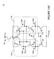
- In addition, the inventions described herein may be applied to any memory architecture and/or layout, including those described and illustrated in Semiconductor Memory Device Patent Application, Semiconductor Memory Device Patent Application II, and/or Semiconductor Memory Cell, Array, Architecture and Device, and Method of Operating Same. The memory architecture may be an open bit line configuration and/or a folded bit line configuration. In those instances where the memory architecture is a folded bit line configuration, it may be advantageous to employ one reference current generator for a pair of bit lines. (See, for example,
FIGS. 16A and 16B ). Notably, the configuration illustrated inFIGS. 16A and 16B may also be implemented in an open bit line architecture. - While a significant portion of this description includes details (for example, clear, write, read and inhibit voltages) directed to N-channel transistors, the inventions (and embodiments thereof described herein are entirely applicable to P-channel transistors. In such embodiments, majority carriers in
body region 18 are electrons and minority carriers are holes. Indeed, the memory arrays may be comprised of N-channel, P-channel and/or both types of transistors. Moreover, the circuitry that is peripheral to the memory array (for example, row and column address decoders, not illustrated herein) may include P-channel and/or N-channel type transistors, including transistors liketransistor 14. - Notably, where P-channel type transistors are employed as
memory cells 12 in the memory array(s), suitable clear, write, read and inhibit voltages are well known to those skilled in the art in light of this disclosure. Accordingly, for sake of brevity, these discussions will not be repeated. - Further, memory cell(s)12 (as well as memory array and matrices58a-n) may also employ the structure, features, attributes, architectures, configurations, materials, techniques and advantages described and illustrated in non-provisional patent application entitled “Semiconductor Device”, which was filed on Feb. 18, 2004, by Fazan and Okhonin, and assigned Ser. No. 10/487,157 (hereinafter “Semiconductor Device Patent Application”). The entire contents of the Semiconductor Device Patent Application, including, for example, the inventions, features, attributes, architectures, configurations, materials, techniques and advantages described and illustrated therein, are hereby incorporated by reference herein.
- As mentioned above, the transistor(s) (for example, the transistor(s) of memory cells12) described herein may be symmetrical or non-symmetrical devices. Where the transistors are symmetrical, the source and drain regions are essentially interchangeable. However, where the transistors are non-symmetrical devices, the source or drain regions of transistors may have different electrical, physical, doping concentration and/or doping profile characteristics. As such, the source or drain regions of the non-symmetrical device are typically not interchangeable.
- Notably, the present invention may also compensate for offset currents and/or voltages that may arise because of transistor mismatch(es) in
sense amplifier 32 due to the feedback or closed-loop control of the reference current. (See, for example,FIG. 7 ). In this way, referencecurrent generators
Claims (24)
Priority Applications (1)
| Application Number | Priority Date | Filing Date | Title |
|---|---|---|---|
| US11/061,069US6980461B2 (en) | 2003-05-13 | 2005-02-18 | Reference current generator, and method of programming, adjusting and/or operating same |
Applications Claiming Priority (4)
| Application Number | Priority Date | Filing Date | Title |
|---|---|---|---|
| US47046203P | 2003-05-13 | 2003-05-13 | |
| US47027603P | 2003-05-14 | 2003-05-14 | |
| US10/840,902US6912150B2 (en) | 2003-05-13 | 2004-05-07 | Reference current generator, and method of programming, adjusting and/or operating same |
| US11/061,069US6980461B2 (en) | 2003-05-13 | 2005-02-18 | Reference current generator, and method of programming, adjusting and/or operating same |
Related Parent Applications (1)
| Application Number | Title | Priority Date | Filing Date |
|---|---|---|---|
| US10/840,902DivisionUS6912150B2 (en) | 2003-05-13 | 2004-05-07 | Reference current generator, and method of programming, adjusting and/or operating same |
Publications (2)
| Publication Number | Publication Date |
|---|---|
| US20050162931A1true US20050162931A1 (en) | 2005-07-28 |
| US6980461B2 US6980461B2 (en) | 2005-12-27 |
Family
ID=33425219
Family Applications (2)
| Application Number | Title | Priority Date | Filing Date |
|---|---|---|---|
| US10/840,902Expired - LifetimeUS6912150B2 (en) | 2003-05-13 | 2004-05-07 | Reference current generator, and method of programming, adjusting and/or operating same |
| US11/061,069Expired - LifetimeUS6980461B2 (en) | 2003-05-13 | 2005-02-18 | Reference current generator, and method of programming, adjusting and/or operating same |
Family Applications Before (1)
| Application Number | Title | Priority Date | Filing Date |
|---|---|---|---|
| US10/840,902Expired - LifetimeUS6912150B2 (en) | 2003-05-13 | 2004-05-07 | Reference current generator, and method of programming, adjusting and/or operating same |
Country Status (5)
| Country | Link |
|---|---|
| US (2) | US6912150B2 (en) |
| EP (1) | EP1620859B1 (en) |
| AT (1) | ATE397779T1 (en) |
| DE (1) | DE602004014269D1 (en) |
| WO (1) | WO2004102631A2 (en) |
Cited By (6)
| Publication number | Priority date | Publication date | Assignee | Title |
|---|---|---|---|---|
| US20090295359A1 (en)* | 2008-05-30 | 2009-12-03 | Paolo Del Croce | System and Method for Providing a Low-Power Self-Adjusting Reference Current for Floating Supply Stages |
| US20100079127A1 (en)* | 2008-09-29 | 2010-04-01 | Active-Semi, Inc. | Regulating current output from a buck converter without external current sensing |
| US20110085364A1 (en)* | 2009-10-08 | 2011-04-14 | Renesas Electronics Corporation | Semiconductor signal processing apparatus |
| US20110110175A1 (en)* | 2009-11-12 | 2011-05-12 | National Tsing Hua University | Memory refresh system and operating method thereof |
| US20110188295A1 (en)* | 2010-02-01 | 2011-08-04 | International Business Machines Corporation | High Performance eDRAM Sense Amplifier |
| WO2013148357A1 (en)* | 2012-03-30 | 2013-10-03 | Silicon Storage Technology, Inc. | Trimmable reference generator for sense amplifier |
Families Citing this family (84)
| Publication number | Priority date | Publication date | Assignee | Title |
|---|---|---|---|---|
| US6912150B2 (en)* | 2003-05-13 | 2005-06-28 | Lionel Portman | Reference current generator, and method of programming, adjusting and/or operating same |
| JP4110115B2 (en)* | 2004-04-15 | 2008-07-02 | 株式会社東芝 | Semiconductor memory device |
| US7035131B2 (en)* | 2004-05-06 | 2006-04-25 | Taiwan Semiconductor Manufacturing Co., Ltd. | Dynamic random access memory cell leakage current detector |
| US7177220B2 (en)* | 2004-05-07 | 2007-02-13 | Taiwan Semiconductor Manufacturing Co., Ltd | Refresh counter with dynamic tracking of process, voltage and temperature variation for semiconductor memory |
| JP4195427B2 (en)* | 2004-08-31 | 2008-12-10 | 株式会社東芝 | Semiconductor memory device |
| JP4083160B2 (en)* | 2004-10-04 | 2008-04-30 | 株式会社東芝 | Semiconductor memory device and driving method of FBC memory cell |
| US7301838B2 (en)* | 2004-12-13 | 2007-11-27 | Innovative Silicon S.A. | Sense amplifier circuitry and architecture to write data into and/or read from memory cells |
| US7301803B2 (en)* | 2004-12-22 | 2007-11-27 | Innovative Silicon S.A. | Bipolar reading technique for a memory cell having an electrically floating body transistor |
| JP4772363B2 (en)* | 2005-04-12 | 2011-09-14 | 株式会社東芝 | Nonvolatile semiconductor memory device |
| JP2006294144A (en)* | 2005-04-12 | 2006-10-26 | Toshiba Corp | Nonvolatile semiconductor memory device |
| US7956669B2 (en)* | 2005-04-15 | 2011-06-07 | International Business Machines Corporation | High-density low-power data retention power gating with double-gate devices |
| US20070023833A1 (en)* | 2005-07-28 | 2007-02-01 | Serguei Okhonin | Method for reading a memory cell having an electrically floating body transistor, and memory cell and array implementing same |
| US7606066B2 (en)* | 2005-09-07 | 2009-10-20 | Innovative Silicon Isi Sa | Memory cell and memory cell array having an electrically floating body transistor, and methods of operating same |
| US7355916B2 (en)* | 2005-09-19 | 2008-04-08 | Innovative Silicon S.A. | Method and circuitry to generate a reference current for reading a memory cell, and device implementing same |
| US7542345B2 (en)* | 2006-02-16 | 2009-06-02 | Innovative Silicon Isi Sa | Multi-bit memory cell having electrically floating body transistor, and method of programming and reading same |
| US7492632B2 (en) | 2006-04-07 | 2009-02-17 | Innovative Silicon Isi Sa | Memory array having a programmable word length, and method of operating same |
| US7606098B2 (en)* | 2006-04-18 | 2009-10-20 | Innovative Silicon Isi Sa | Semiconductor memory array architecture with grouped memory cells, and method of controlling same |
| US7933142B2 (en) | 2006-05-02 | 2011-04-26 | Micron Technology, Inc. | Semiconductor memory cell and array using punch-through to program and read same |
| US7499352B2 (en)* | 2006-05-19 | 2009-03-03 | Innovative Silicon Isi Sa | Integrated circuit having memory array including row redundancy, and method of programming, controlling and/or operating same |
| US8069377B2 (en) | 2006-06-26 | 2011-11-29 | Micron Technology, Inc. | Integrated circuit having memory array including ECC and column redundancy and method of operating the same |
| US7542340B2 (en) | 2006-07-11 | 2009-06-02 | Innovative Silicon Isi Sa | Integrated circuit including memory array having a segmented bit line architecture and method of controlling and/or operating same |
| US7733707B2 (en)* | 2006-07-21 | 2010-06-08 | Hynix Semiconductor Inc. | 1-transistor type DRAM cell, DRAM device and DRAM comprising thereof and driving method thereof and manufacturing method thereof |
| US7645617B2 (en)* | 2006-07-27 | 2010-01-12 | Hynix Semiconductor, Inc. | Nonvolatile ferroelectric memory device using silicon substrate, method for manufacturing the same, and refresh method thereof |
| US7932547B2 (en)* | 2006-07-27 | 2011-04-26 | Hynix Semiconductor Inc. | Nonvolatile ferroelectric memory device using silicon substrate, method for manufacturing the same, and refresh method thereof |
| US7410856B2 (en)* | 2006-09-14 | 2008-08-12 | Micron Technology, Inc. | Methods of forming vertical transistors |
| US8514622B2 (en) | 2007-11-29 | 2013-08-20 | Zeno Semiconductor, Inc. | Compact semiconductor memory device having reduced number of contacts, methods of operating and methods of making |
| US9601493B2 (en) | 2006-11-29 | 2017-03-21 | Zeno Semiconductor, Inc | Compact semiconductor memory device having reduced number of contacts, methods of operating and methods of making |
| US8547756B2 (en) | 2010-10-04 | 2013-10-01 | Zeno Semiconductor, Inc. | Semiconductor memory device having an electrically floating body transistor |
| US9391079B2 (en) | 2007-11-29 | 2016-07-12 | Zeno Semiconductor, Inc. | Compact semiconductor memory device having reduced number of contacts, methods of operating and methods of making |
| US7724578B2 (en)* | 2006-12-15 | 2010-05-25 | Globalfoundries Inc. | Sensing device for floating body cell memory and method thereof |
| KR101277402B1 (en) | 2007-01-26 | 2013-06-20 | 마이크론 테크놀로지, 인코포레이티드 | Floating-body dram transistor comprising source/drain regions separated from the gated body region |
| US8518774B2 (en) | 2007-03-29 | 2013-08-27 | Micron Technology, Inc. | Manufacturing process for zero-capacitor random access memory circuits |
| US7408800B1 (en) | 2007-05-03 | 2008-08-05 | International Business Machines Corporation | Apparatus and method for improved SRAM device performance through double gate topology |
| US20080273366A1 (en)* | 2007-05-03 | 2008-11-06 | International Business Machines Corporation | Design structure for improved sram device performance through double gate topology |
| US8064274B2 (en) | 2007-05-30 | 2011-11-22 | Micron Technology, Inc. | Integrated circuit having voltage generation circuitry for memory cell array, and method of operating and/or controlling same |
| US8085594B2 (en) | 2007-06-01 | 2011-12-27 | Micron Technology, Inc. | Reading technique for memory cell with electrically floating body transistor |
| WO2009039169A1 (en) | 2007-09-17 | 2009-03-26 | Innovative Silicon S.A. | Refreshing data of memory cells with electrically floating body transistors |
| US20090078999A1 (en)* | 2007-09-20 | 2009-03-26 | Anderson Brent A | Semiconductor device structures with floating body charge storage and methods for forming such semiconductor device structures. |
| JP2009093708A (en)* | 2007-10-04 | 2009-04-30 | Toshiba Corp | Semiconductor memory device and driving method thereof |
| US8536628B2 (en) | 2007-11-29 | 2013-09-17 | Micron Technology, Inc. | Integrated circuit having memory cell array including barriers, and method of manufacturing same |
| US8349662B2 (en) | 2007-12-11 | 2013-01-08 | Micron Technology, Inc. | Integrated circuit having memory cell array, and method of manufacturing same |
| US8773933B2 (en) | 2012-03-16 | 2014-07-08 | Micron Technology, Inc. | Techniques for accessing memory cells |
| US8014195B2 (en)* | 2008-02-06 | 2011-09-06 | Micron Technology, Inc. | Single transistor memory cell |
| US8189376B2 (en) | 2008-02-08 | 2012-05-29 | Micron Technology, Inc. | Integrated circuit having memory cells including gate material having high work function, and method of manufacturing same |
| US7957206B2 (en) | 2008-04-04 | 2011-06-07 | Micron Technology, Inc. | Read circuitry for an integrated circuit having memory cells and/or a memory cell array, and method of operating same |
| JP6053250B2 (en)* | 2008-06-12 | 2016-12-27 | ピーエスフォー ルクスコ エスエイアールエルPS4 Luxco S.a.r.l. | Semiconductor device |
| US7947543B2 (en) | 2008-09-25 | 2011-05-24 | Micron Technology, Inc. | Recessed gate silicon-on-insulator floating body device with self-aligned lateral isolation |
| US7933140B2 (en) | 2008-10-02 | 2011-04-26 | Micron Technology, Inc. | Techniques for reducing a voltage swing |
| US7924630B2 (en) | 2008-10-15 | 2011-04-12 | Micron Technology, Inc. | Techniques for simultaneously driving a plurality of source lines |
| US8223574B2 (en) | 2008-11-05 | 2012-07-17 | Micron Technology, Inc. | Techniques for block refreshing a semiconductor memory device |
| US8213226B2 (en)* | 2008-12-05 | 2012-07-03 | Micron Technology, Inc. | Vertical transistor memory cell and array |
| US8319294B2 (en) | 2009-02-18 | 2012-11-27 | Micron Technology, Inc. | Techniques for providing a source line plane |
| WO2010102106A2 (en) | 2009-03-04 | 2010-09-10 | Innovative Silicon Isi Sa | Techniques for forming a contact to a buried diffusion layer in a semiconductor memory device |
| US8748959B2 (en) | 2009-03-31 | 2014-06-10 | Micron Technology, Inc. | Semiconductor memory device |
| US8139418B2 (en) | 2009-04-27 | 2012-03-20 | Micron Technology, Inc. | Techniques for controlling a direct injection semiconductor memory device |
| US8508994B2 (en) | 2009-04-30 | 2013-08-13 | Micron Technology, Inc. | Semiconductor device with floating gate and electrically floating body |
| US8498157B2 (en)* | 2009-05-22 | 2013-07-30 | Micron Technology, Inc. | Techniques for providing a direct injection semiconductor memory device |
| US8537610B2 (en) | 2009-07-10 | 2013-09-17 | Micron Technology, Inc. | Techniques for providing a semiconductor memory device |
| US9076543B2 (en) | 2009-07-27 | 2015-07-07 | Micron Technology, Inc. | Techniques for providing a direct injection semiconductor memory device |
| US8199595B2 (en) | 2009-09-04 | 2012-06-12 | Micron Technology, Inc. | Techniques for sensing a semiconductor memory device |
| US8174881B2 (en) | 2009-11-24 | 2012-05-08 | Micron Technology, Inc. | Techniques for reducing disturbance in a semiconductor device |
| US8310893B2 (en) | 2009-12-16 | 2012-11-13 | Micron Technology, Inc. | Techniques for reducing impact of array disturbs in a semiconductor memory device |
| US8416636B2 (en) | 2010-02-12 | 2013-04-09 | Micron Technology, Inc. | Techniques for controlling a semiconductor memory device |
| US10461084B2 (en) | 2010-03-02 | 2019-10-29 | Zeno Semiconductor, Inc. | Compact semiconductor memory device having reduced number of contacts, methods of operating and methods of making |
| US9922981B2 (en) | 2010-03-02 | 2018-03-20 | Zeno Semiconductor, Inc. | Compact semiconductor memory device having reduced number of contacts, methods of operating and methods of making |
| US8411513B2 (en) | 2010-03-04 | 2013-04-02 | Micron Technology, Inc. | Techniques for providing a semiconductor memory device having hierarchical bit lines |
| US8576631B2 (en) | 2010-03-04 | 2013-11-05 | Micron Technology, Inc. | Techniques for sensing a semiconductor memory device |
| US8369177B2 (en) | 2010-03-05 | 2013-02-05 | Micron Technology, Inc. | Techniques for reading from and/or writing to a semiconductor memory device |
| US8547738B2 (en) | 2010-03-15 | 2013-10-01 | Micron Technology, Inc. | Techniques for providing a semiconductor memory device |
| US8411524B2 (en) | 2010-05-06 | 2013-04-02 | Micron Technology, Inc. | Techniques for refreshing a semiconductor memory device |
| WO2012058324A2 (en) | 2010-10-29 | 2012-05-03 | Rambus Inc. | Resistance change memory cell circuits and methods |
| FR2967522B1 (en)* | 2010-11-12 | 2012-12-21 | St Microelectronics Sa | SECURE NON-VOLATILE MEMORY |
| US8531878B2 (en) | 2011-05-17 | 2013-09-10 | Micron Technology, Inc. | Techniques for providing a semiconductor memory device |
| US9559216B2 (en) | 2011-06-06 | 2017-01-31 | Micron Technology, Inc. | Semiconductor memory device and method for biasing same |
| US8885428B2 (en)* | 2013-02-22 | 2014-11-11 | Sandisk 3D Llc | Smart read scheme for memory array sensing |
| US9029922B2 (en) | 2013-03-09 | 2015-05-12 | Zeno Semiconductor, Inc. | Memory device comprising electrically floating body transistor |
| US9275723B2 (en) | 2013-04-10 | 2016-03-01 | Zeno Semiconductor, Inc. | Scalable floating body memory cell for memory compilers and method of using floating body memories with memory compilers |
| US9368625B2 (en) | 2013-05-01 | 2016-06-14 | Zeno Semiconductor, Inc. | NAND string utilizing floating body memory cell |
| GB2529861A (en) | 2014-09-04 | 2016-03-09 | Ibm | Current-mode sense amplifier |
| US9851738B2 (en) | 2015-08-13 | 2017-12-26 | Arm Ltd. | Programmable voltage reference |
| US9748943B2 (en) | 2015-08-13 | 2017-08-29 | Arm Ltd. | Programmable current for correlated electron switch |
| US9979385B2 (en)* | 2015-10-05 | 2018-05-22 | Arm Ltd. | Circuit and method for monitoring correlated electron switches |
| US9508397B1 (en)* | 2015-12-03 | 2016-11-29 | Freescale Semiconductor, Inc. | Non-volatile memory (NVM) with endurance control |
| US11062772B2 (en) | 2017-12-29 | 2021-07-13 | Panasonic Corporation | Variable resistance non-volatile memory device |
Citations (87)
| Publication number | Priority date | Publication date | Assignee | Title |
|---|---|---|---|---|
| US3439214A (en)* | 1968-03-04 | 1969-04-15 | Fairchild Camera Instr Co | Beam-junction scan converter |
| US4032947A (en)* | 1971-10-20 | 1977-06-28 | Siemens Aktiengesellschaft | Controllable charge-coupled semiconductor device |
| US4250569A (en)* | 1978-11-15 | 1981-02-10 | Fujitsu Limited | Semiconductor memory device |
| US4262340A (en)* | 1978-11-14 | 1981-04-14 | Fujitsu Limited | Semiconductor memory device |
| US4371955A (en)* | 1979-02-22 | 1983-02-01 | Fujitsu Limited | Charge-pumping MOS FET memory device |
| US4527181A (en)* | 1980-08-28 | 1985-07-02 | Fujitsu Limited | High density semiconductor memory array and method of making same |
| US5388068A (en)* | 1990-05-02 | 1995-02-07 | Microelectronics & Computer Technology Corp. | Superconductor-semiconductor hybrid memory circuits with superconducting three-terminal switching devices |
| US5446299A (en)* | 1994-04-29 | 1995-08-29 | International Business Machines Corporation | Semiconductor random access memory cell on silicon-on-insulator with dual control gates |
| US5489792A (en)* | 1994-04-07 | 1996-02-06 | Regents Of The University Of California | Silicon-on-insulator transistors having improved current characteristics and reduced electrostatic discharge susceptibility |
| US5528062A (en)* | 1992-06-17 | 1996-06-18 | International Business Machines Corporation | High-density DRAM structure on soi |
| US5593912A (en)* | 1994-10-06 | 1997-01-14 | International Business Machines Corporation | SOI trench DRAM cell for 256 MB DRAM and beyond |
| US5606188A (en)* | 1995-04-26 | 1997-02-25 | International Business Machines Corporation | Fabrication process and structure for a contacted-body silicon-on-insulator dynamic random access memory |
| US5627092A (en)* | 1994-09-26 | 1997-05-06 | Siemens Aktiengesellschaft | Deep trench dram process on SOI for low leakage DRAM cell |
| US5631186A (en)* | 1992-12-30 | 1997-05-20 | Samsung Electronics Co., Ltd. | Method for making a dynamic random access memory using silicon-on-insulator techniques |
| US5740099A (en)* | 1995-02-07 | 1998-04-14 | Nec Corporation | Semiconductor memory device having peripheral circuit and interface circuit fabricated on bulk region out of silicon-on-insulator region for memory cells |
| US5778243A (en)* | 1996-07-03 | 1998-07-07 | International Business Machines Corporation | Multi-threaded cell for a memory |
| US5780906A (en)* | 1995-06-21 | 1998-07-14 | Micron Technology, Inc. | Static memory cell and method of manufacturing a static memory cell |
| US5784311A (en)* | 1997-06-13 | 1998-07-21 | International Business Machines Corporation | Two-device memory cell on SOI for merged logic and memory applications |
| US5877978A (en)* | 1996-03-04 | 1999-03-02 | Mitsubishi Denki Kabushiki Kaisha | Semiconductor memory device |
| US5886376A (en)* | 1996-07-01 | 1999-03-23 | International Business Machines Corporation | EEPROM having coplanar on-insulator FET and control gate |
| US5886385A (en)* | 1996-08-22 | 1999-03-23 | Kabushiki Kaisha Toshiba | Semiconductor device and manufacturing method thereof |
| US5897351A (en)* | 1997-02-20 | 1999-04-27 | Micron Technology, Inc. | Method for forming merged transistor structure for gain memory cell |
| US5930648A (en)* | 1996-12-30 | 1999-07-27 | Hyundai Electronics Industries Co., Ltd. | Semiconductor memory device having different substrate thickness between memory cell area and peripheral area and manufacturing method thereof |
| US5929479A (en)* | 1996-10-21 | 1999-07-27 | Nec Corporation | Floating gate type non-volatile semiconductor memory for storing multi-value information |
| US5936265A (en)* | 1996-03-25 | 1999-08-10 | Kabushiki Kaisha Toshiba | Semiconductor device including a tunnel effect element |
| US5943258A (en)* | 1997-12-24 | 1999-08-24 | Texas Instruments Incorporated | Memory with storage cells having SOI drive and access transistors with tied floating body connections |
| US5943581A (en)* | 1997-11-05 | 1999-08-24 | Vanguard International Semiconductor Corporation | Method of fabricating a buried reservoir capacitor structure for high-density dynamic random access memory (DRAM) circuits |
| US6018172A (en)* | 1994-09-26 | 2000-01-25 | Mitsubishi Denki Kabushiki Kaisha | Semiconductor memory device including memory cell transistors formed on SOI substrate and having fixed body regions |
| US6096598A (en)* | 1998-10-29 | 2000-08-01 | International Business Machines Corporation | Method for forming pillar memory cells and device formed thereby |
| US6097058A (en)* | 1997-05-23 | 2000-08-01 | Rohm Co., Ltd. | Ferroelectric memory device and a method of manufacturing thereof |
| US6111778A (en)* | 1999-05-10 | 2000-08-29 | International Business Machines Corporation | Body contacted dynamic memory |
| US6171923B1 (en)* | 1997-11-20 | 2001-01-09 | Vanguard International Semiconductor Corporation | Method for fabricating a DRAM cell structure on an SOI wafer incorporating a two dimensional trench capacitor |
| US6177708B1 (en)* | 1998-08-07 | 2001-01-23 | International Business Machines Corporation | SOI FET body contact structure |
| US6214694B1 (en)* | 1998-11-17 | 2001-04-10 | International Business Machines Corporation | Process of making densely patterned silicon-on-insulator (SOI) region on a wafer |
| US6225158B1 (en)* | 1998-05-28 | 2001-05-01 | International Business Machines Corporation | Trench storage dynamic random access memory cell with vertical transfer device |
| US6245613B1 (en)* | 1998-04-28 | 2001-06-12 | International Business Machines Corporation | Field effect transistor having a floating gate |
| US6252281B1 (en)* | 1995-03-27 | 2001-06-26 | Kabushiki Kaisha Toshiba | Semiconductor device having an SOI substrate |
| US6351426B1 (en)* | 1995-01-20 | 2002-02-26 | Kabushiki Kaisha Toshiba | DRAM having a power supply voltage lowering circuit |
| US6350653B1 (en)* | 2000-10-12 | 2002-02-26 | International Business Machines Corporation | Embedded DRAM on silicon-on-insulator substrate |
| US20020030214A1 (en)* | 2000-09-11 | 2002-03-14 | Fumio Horiguchi | Semiconductor device and method for manufacturing the same |
| US6359802B1 (en)* | 2000-03-28 | 2002-03-19 | Intel Corporation | One-transistor and one-capacitor DRAM cell for logic process technology |
| US20020034855A1 (en)* | 2000-09-08 | 2002-03-21 | Fumio Horiguchi | Semiconductor memory device and its manufacturing method |
| US20020036322A1 (en)* | 2000-03-17 | 2002-03-28 | Ramachandra Divakauni | SOI stacked dram logic |
| US20020051378A1 (en)* | 2000-08-17 | 2002-05-02 | Takashi Ohsawa | Semiconductor memory device and method of manufacturing the same |
| US20020057487A1 (en)* | 1997-07-24 | 2002-05-16 | Scientific Materials Corporation | Optical laser light limiter |
| US6391658B1 (en)* | 1999-10-26 | 2002-05-21 | International Business Machines Corporation | Formation of arrays of microelectronic elements |
| US6403435B1 (en)* | 2000-07-21 | 2002-06-11 | Hyundai Electronics Industries Co., Ltd. | Method for fabricating a semiconductor device having recessed SOI structure |
| US20020070411A1 (en)* | 2000-09-08 | 2002-06-13 | Alcatel | Method of processing a high voltage p++/n-well junction and a device manufactured by the method |
| US20020072155A1 (en)* | 2000-12-08 | 2002-06-13 | Chih-Cheng Liu | Method of fabricating a DRAM unit |
| US20020076880A1 (en)* | 2000-06-12 | 2002-06-20 | Takashi Yamada | Semiconductor device and method of fabricating the same |
| US20020086463A1 (en)* | 2000-12-30 | 2002-07-04 | Houston Theodore W. | Means for forming SOI |
| US20020084913A1 (en)* | 1999-07-07 | 2002-07-04 | Flight Refuelling Limited | Data transmission in pipeline systems |
| US20020089038A1 (en)* | 2000-10-20 | 2002-07-11 | International Business Machines Corporation | Fully-depleted-collector silicon-on-insulator (SOI) bipolar transistor useful alone or in SOI BiCMOS |
| US6424016B1 (en)* | 1996-05-24 | 2002-07-23 | Texas Instruments Incorporated | SOI DRAM having P-doped polysilicon gate for a memory pass transistor |
| US6424011B1 (en)* | 1997-04-14 | 2002-07-23 | International Business Machines Corporation | Mixed memory integration with NVRAM, dram and sram cell structures on same substrate |
| US20020096643A1 (en)* | 1996-02-08 | 2002-07-25 | Bright Solutions, Inc., A Michigan Corporation | Portable light source and system for use in leak detection |
| US6429477B1 (en)* | 2000-10-31 | 2002-08-06 | International Business Machines Corporation | Shared body and diffusion contact structure and method for fabricating same |
| US20020110018A1 (en)* | 2001-02-15 | 2002-08-15 | Takashi Ohsawa | Semiconductor memory device |
| US20020114191A1 (en)* | 2001-02-19 | 2002-08-22 | Yoshihisa Iwata | Semiconductor memory device and method of manufacturing the same |
| US6440872B1 (en)* | 2000-11-03 | 2002-08-27 | International Business Machines Corporation | Method for hybrid DRAM cell utilizing confined strap isolation |
| US6441438B1 (en)* | 1999-02-18 | 2002-08-27 | Taiwan Semiconductor Manufacturing Company | ESD protect device structure |
| US6441435B1 (en)* | 2001-01-31 | 2002-08-27 | Advanced Micro Devices, Inc. | SOI device with wrap-around contact to underside of body, and method of making |
| US20030003608A1 (en)* | 2001-03-21 | 2003-01-02 | Tsunetoshi Arikado | Semiconductor wafer with ID mark, equipment for and method of manufacturing semiconductor device from them |
| US20030015757A1 (en)* | 2001-07-19 | 2003-01-23 | Takashi Ohsawa | Semiconductor memory device |
| US6518105B1 (en)* | 2001-12-10 | 2003-02-11 | Taiwan Semiconductor Manufacturing Company | High performance PD SOI tunneling-biased MOSFET |
| US20030035324A1 (en)* | 2001-08-17 | 2003-02-20 | Kabushiki Kaisha Toshiba | Semiconductor memory device |
| US6531754B1 (en)* | 2001-12-28 | 2003-03-11 | Kabushiki Kaisha Toshiba | Manufacturing method of partial SOI wafer, semiconductor device using the partial SOI wafer and manufacturing method thereof |
| US6532723B2 (en)* | 2000-06-20 | 2003-03-18 | Deere & Company | Agricultural implement constructed for being narrowed for transport |
| US20030057490A1 (en)* | 2001-09-26 | 2003-03-27 | Kabushiki Kaisha Toshiba | Semiconductor device substrate and method of manufacturing semiconductor device substrate |
| US6547848B1 (en)* | 1999-05-26 | 2003-04-15 | Outokumpu Oyj | Method for cooling the gas flow in a smelting furnace |
| US6548848B2 (en)* | 2001-03-15 | 2003-04-15 | Kabushiki Kaisha Toshiba | Semiconductor memory device |
| US6549450B1 (en)* | 2000-11-08 | 2003-04-15 | Ibm Corporation | Method and system for improving the performance on SOI memory arrays in an SRAM architecture system |
| US6552398B2 (en)* | 2001-01-16 | 2003-04-22 | Ibm Corporation | T-Ram array having a planar cell structure and method for fabricating the same |
| US6556477B2 (en)* | 2001-05-21 | 2003-04-29 | Ibm Corporation | Integrated chip having SRAM, DRAM and flash memory and method for fabricating the same |
| US6566177B1 (en)* | 1999-10-25 | 2003-05-20 | International Business Machines Corporation | Silicon-on-insulator vertical array device trench capacitor DRAM |
| US20030102497A1 (en)* | 2001-12-04 | 2003-06-05 | International Business Machines Corporation | Multiple-plane finFET CMOS |
| US20030123279A1 (en)* | 2002-01-03 | 2003-07-03 | International Business Machines Corporation | Silicon-on-insulator SRAM cells with increased stability and yield |
| US20030151112A1 (en)* | 2002-02-13 | 2003-08-14 | Takashi Yamada | Semiconductor device having one of patterned SOI and SON structure |
| US20040021137A1 (en)* | 2001-06-18 | 2004-02-05 | Pierre Fazan | Semiconductor device |
| US20040042268A1 (en)* | 2002-08-30 | 2004-03-04 | Arup Bhattacharyya | One-device non-volatile random access memory cell |
| US20040041208A1 (en)* | 2002-08-30 | 2004-03-04 | Arup Bhattacharyya | One transistor SOI non-volatile random access memory cell |
| US20040052142A1 (en)* | 2002-09-18 | 2004-03-18 | Kabushiki Kaisha Toshiba | Semiconductor memory device and method of controlling the same |
| US6721222B2 (en)* | 2000-10-17 | 2004-04-13 | Intel Corporation | Noise suppression for open bit line DRAM architectures |
| US20040108532A1 (en)* | 2002-12-04 | 2004-06-10 | Micron Technology, Inc. | Embedded DRAM gain memory cell |
| US6850585B2 (en)* | 2003-03-05 | 2005-02-01 | Ge Medical Systems Global Technology Company, Llc | Progressive updating approach for volumetric CT image reconstruction |
| US20050135169A1 (en)* | 2003-12-22 | 2005-06-23 | Intel Corporation | Method and apparatus to generate a reference value in a memory array |
| US6912150B2 (en)* | 2003-05-13 | 2005-06-28 | Lionel Portman | Reference current generator, and method of programming, adjusting and/or operating same |
Family Cites Families (107)
| Publication number | Priority date | Publication date | Assignee | Title |
|---|---|---|---|---|
| IT979035B (en) | 1972-04-25 | 1974-09-30 | Ibm | INTEGRATED CIRCUIT DEVICE FOR STORING BINARY INFORMATION WITH ELECTRO-LUMINESCENT EMISSION |
| FR2197494A5 (en) | 1972-08-25 | 1974-03-22 | Radiotechnique Compelec | |
| US3997799A (en) | 1975-09-15 | 1976-12-14 | Baker Roger T | Semiconductor-device for the storage of binary data |
| DE3065928D1 (en) | 1979-01-25 | 1984-01-26 | Nec Corp | Semiconductor memory device |
| EP0030856B1 (en) | 1979-12-13 | 1984-03-21 | Fujitsu Limited | Charge-pumping semiconductor memory cell comprising a charge-storage region and memory device using such a cell |
| JPS5982761A (en) | 1982-11-04 | 1984-05-12 | Hitachi Ltd | semiconductor memory |
| JPS6070760A (en) | 1983-09-27 | 1985-04-22 | Fujitsu Ltd | Semiconductor memory device |
| JPS6177359A (en) | 1984-09-21 | 1986-04-19 | Fujitsu Ltd | semiconductor storage device |
| JPS61280651A (en) | 1985-05-24 | 1986-12-11 | Fujitsu Ltd | semiconductor storage device |
| JPH0671067B2 (en) | 1985-11-20 | 1994-09-07 | 株式会社日立製作所 | Semiconductor device |
| JPS62272561A (en) | 1986-05-20 | 1987-11-26 | Seiko Epson Corp | 1 transistor memory cell |
| JPS6319847A (en) | 1986-07-14 | 1988-01-27 | Oki Electric Ind Co Ltd | Semiconductor memory device |
| US4816884A (en) | 1987-07-20 | 1989-03-28 | International Business Machines Corporation | High density vertical trench transistor and capacitor memory cell structure and fabrication method therefor |
| JP2582794B2 (en) | 1987-08-10 | 1997-02-19 | 株式会社東芝 | Semiconductor device and manufacturing method thereof |
| DE68926793T2 (en) | 1988-03-15 | 1997-01-09 | Toshiba Kawasaki Kk | Dynamic RAM |
| JPH0666443B2 (en) | 1988-07-07 | 1994-08-24 | 株式会社東芝 | Semiconductor memory cell and semiconductor memory |
| US4910709A (en) | 1988-08-10 | 1990-03-20 | International Business Machines Corporation | Complementary metal-oxide-semiconductor transistor and one-capacitor dynamic-random-access memory cell |
| US5144390A (en)* | 1988-09-02 | 1992-09-01 | Texas Instruments Incorporated | Silicon-on insulator transistor with internal body node to source node connection |
| US5258635A (en) | 1988-09-06 | 1993-11-02 | Kabushiki Kaisha Toshiba | MOS-type semiconductor integrated circuit device |
| JPH02168496A (en) | 1988-09-14 | 1990-06-28 | Kawasaki Steel Corp | Semiconductor memory circuit |
| NL8802423A (en) | 1988-10-03 | 1990-05-01 | Imec Inter Uni Micro Electr | METHOD FOR OPERATING A MOSS STRUCTURE AND MOSS STRUCTURE SUITABLE FOR IT. |
| US4894697A (en) | 1988-10-31 | 1990-01-16 | International Business Machines Corporation | Ultra dense dram cell and its method of fabrication |
| JPH02294076A (en) | 1989-05-08 | 1990-12-05 | Hitachi Ltd | Semiconductor integrated circuit device |
| JPH03171768A (en) | 1989-11-30 | 1991-07-25 | Toshiba Corp | semiconductor storage device |
| US5366917A (en) | 1990-03-20 | 1994-11-22 | Nec Corporation | Method for fabricating polycrystalline silicon having micro roughness on the surface |
| DE69111929T2 (en) | 1990-07-09 | 1996-03-28 | Sony Corp | Semiconductor device on a dielectric insulated substrate. |
| US5331197A (en) | 1991-04-23 | 1994-07-19 | Canon Kabushiki Kaisha | Semiconductor memory device including gate electrode sandwiching a channel region |
| US5424567A (en) | 1991-05-15 | 1995-06-13 | North American Philips Corporation | Protected programmable transistor with reduced parasitic capacitances and method of fabrication |
| EP0537677B1 (en) | 1991-10-16 | 1998-08-19 | Sony Corporation | Method of forming an SOI structure with a DRAM |
| EP0836194B1 (en) | 1992-03-30 | 2000-05-24 | Mitsubishi Denki Kabushiki Kaisha | Semiconductor device |
| EP0599388B1 (en) | 1992-11-20 | 2000-08-02 | Koninklijke Philips Electronics N.V. | Semiconductor device provided with a programmable element |
| JPH06216338A (en) | 1992-11-27 | 1994-08-05 | Internatl Business Mach Corp <Ibm> | Semiconductor memory cell and its preparation |
| JPH0799251A (en) | 1992-12-10 | 1995-04-11 | Sony Corp | Semiconductor memory cell |
| JP3613594B2 (en) | 1993-08-19 | 2005-01-26 | 株式会社ルネサステクノロジ | Semiconductor element and semiconductor memory device using the same |
| US5448513A (en)* | 1993-12-02 | 1995-09-05 | Regents Of The University Of California | Capacitorless DRAM device on silicon-on-insulator substrate |
| JP3273582B2 (en) | 1994-05-13 | 2002-04-08 | キヤノン株式会社 | Storage device |
| JPH0832040A (en) | 1994-07-14 | 1996-02-02 | Nec Corp | Semiconductor device |
| FR2726935B1 (en) | 1994-11-10 | 1996-12-13 | Commissariat Energie Atomique | ELECTRICALLY ERASABLE NON-VOLATILE MEMORY DEVICE AND METHOD FOR PRODUCING SUCH A DEVICE |
| JP3315293B2 (en) | 1995-01-05 | 2002-08-19 | 株式会社東芝 | Semiconductor storage device |
| US6292424B1 (en)* | 1995-01-20 | 2001-09-18 | Kabushiki Kaisha Toshiba | DRAM having a power supply voltage lowering circuit |
| DE69524558T2 (en)* | 1995-01-27 | 2002-07-18 | Stmicroelectronics S.R.L., Agrate Brianza | Sectional approximation method for scanning non-volatile multi-level memory cells and corresponding scanning circuit |
| JP3407232B2 (en) | 1995-02-08 | 2003-05-19 | 富士通株式会社 | Semiconductor memory device and operation method thereof |
| JPH08222648A (en) | 1995-02-14 | 1996-08-30 | Canon Inc | Storage device |
| EP0727820B1 (en) | 1995-02-17 | 2004-03-24 | Hitachi, Ltd. | Semiconductor memory device and method of manufacturing the same |
| JPH08274277A (en) | 1995-03-31 | 1996-10-18 | Toyota Central Res & Dev Lab Inc | Semiconductor memory device and manufacturing method thereof |
| US5568356A (en)* | 1995-04-18 | 1996-10-22 | Hughes Aircraft Company | Stacked module assembly including electrically interconnected switching module and plural electronic modules |
| EP0739097B1 (en) | 1995-04-21 | 2004-04-07 | Nippon Telegraph And Telephone Corporation | MOSFET circuit and CMOS logic circuit using the same |
| DE19519159C2 (en) | 1995-05-24 | 1998-07-09 | Siemens Ag | DRAM cell arrangement and method for its production |
| EP0744722B1 (en) | 1995-05-24 | 2001-07-18 | Innovative Sputtering Technology N.V. (I.S.T.) | Magnetic antipilferage tag |
| JPH0946688A (en) | 1995-07-26 | 1997-02-14 | Fujitsu Ltd | Video information provision / reception system |
| DE69516402T2 (en)* | 1995-07-31 | 2000-11-02 | Stmicroelectronics S.R.L., Agrate Brianza | Mixed serial parallel dichotomic reading method for non-volatile multilevel memory cells and reading circuit using such a method |
| JPH0982912A (en) | 1995-09-13 | 1997-03-28 | Toshiba Corp | Semiconductor memory device and manufacturing method thereof |
| US5585285A (en) | 1995-12-06 | 1996-12-17 | Micron Technology, Inc. | Method of forming dynamic random access memory circuitry using SOI and isolation trenches |
| DE19603810C1 (en) | 1996-02-02 | 1997-08-28 | Siemens Ag | Memory cell arrangement and method for its production |
| US6307236B1 (en) | 1996-04-08 | 2001-10-23 | Hitachi, Ltd. | Semiconductor integrated circuit device |
| EP0801427A3 (en) | 1996-04-11 | 1999-05-06 | Matsushita Electric Industrial Co., Ltd. | Field effect transistor, semiconductor storage device, method of manufacturing the same and method of driving semiconductor storage device |
| EP0811986B1 (en)* | 1996-06-05 | 2003-03-12 | STMicroelectronics S.r.l. | Page-mode memory device with multiple-level memory cells |
| US5811283A (en)* | 1996-08-13 | 1998-09-22 | United Microelectronics Corporation | Silicon on insulator (SOI) dram cell structure and process |
| JP3602939B2 (en) | 1996-11-19 | 2004-12-15 | 松下電器産業株式会社 | Semiconductor storage device |
| JP3161354B2 (en) | 1997-02-07 | 2001-04-25 | 日本電気株式会社 | Semiconductor device and manufacturing method thereof |
| EP0860878A2 (en) | 1997-02-20 | 1998-08-26 | Texas Instruments Incorporated | An integrated circuit with programmable elements |
| JP3441330B2 (en) | 1997-02-28 | 2003-09-02 | 株式会社東芝 | Semiconductor device and manufacturing method thereof |
| JPH11191596A (en) | 1997-04-02 | 1999-07-13 | Sony Corp | Semiconductor memory cell and method of manufacturing the same |
| US5881010A (en) | 1997-05-15 | 1999-03-09 | Stmicroelectronics, Inc. | Multiple transistor dynamic random access memory array architecture with simultaneous refresh of multiple memory cells during a read operation |
| JPH1187649A (en) | 1997-09-04 | 1999-03-30 | Hitachi Ltd | Semiconductor storage device |
| US6262625B1 (en) | 1999-10-29 | 2001-07-17 | Hewlett-Packard Co | Operational amplifier with digital offset calibration |
| DE19752968C1 (en) | 1997-11-28 | 1999-06-24 | Siemens Ag | Memory cell arrangement and method for its production |
| JP3378879B2 (en) | 1997-12-10 | 2003-02-17 | 松下電器産業株式会社 | Nonvolatile semiconductor memory device and driving method thereof |
| DE59814170D1 (en) | 1997-12-17 | 2008-04-03 | Qimonda Ag | Memory cell arrangement and method for its production |
| JP4030198B2 (en) | 1998-08-11 | 2008-01-09 | 株式会社ルネサステクノロジ | Manufacturing method of semiconductor integrated circuit device |
| KR100268419B1 (en)* | 1998-08-14 | 2000-10-16 | 윤종용 | A high integrated semiconductor memory device and method fabricating the same |
| US6423596B1 (en) | 1998-09-29 | 2002-07-23 | Texas Instruments Incorporated | Method for two-sided fabrication of a memory array |
| KR100290787B1 (en) | 1998-12-26 | 2001-07-12 | 박종섭 | Manufacturing Method of Semiconductor Memory Device |
| US6535415B2 (en) | 1999-02-22 | 2003-03-18 | Hitachi, Ltd. | Semiconductor device |
| JP3384350B2 (en) | 1999-03-01 | 2003-03-10 | 株式会社村田製作所 | Method for producing low-temperature sintered ceramic composition |
| DE19912108A1 (en) | 1999-03-18 | 2000-09-28 | Porsche Ag | Lubricant reservoir for an internal combustion engine |
| US6157216A (en) | 1999-04-22 | 2000-12-05 | International Business Machines Corporation | Circuit driver on SOI for merged logic and memory circuits |
| IT1312471B1 (en)* | 1999-05-11 | 2002-04-17 | St Microelectronics Srl | METHOD OF VERIFICATION IN WRITING OF THE THRESHOLD VALUE IN NON-VOLATILE MEMORIES |
| US6333532B1 (en) | 1999-07-16 | 2001-12-25 | International Business Machines Corporation | Patterned SOI regions in semiconductor chips |
| JP2001044391A (en) | 1999-07-29 | 2001-02-16 | Fujitsu Ltd | Semiconductor memory device and manufacturing method thereof |
| IT1308857B1 (en)* | 1999-10-29 | 2002-01-11 | St Microelectronics Srl | READING METHOD AND CIRCUIT FOR A NON-VOLATILE MEMORY. |
| JP2001180633A (en) | 1999-12-27 | 2001-07-03 | Toshiba Tec Corp | Label printer |
| DE10012846A1 (en) | 2000-03-16 | 2001-09-27 | Fico Itm Sa | Flocked sun visor for motor vehicle; has sun visor body with hard, smooth surface, preferably of blow-moulded plastics, which is coated with adhesive and is flocked by electrostatic action |
| JP2002064150A (en) | 2000-06-05 | 2002-02-28 | Mitsubishi Electric Corp | Semiconductor device |
| DE10028424C2 (en) | 2000-06-06 | 2002-09-19 | Infineon Technologies Ag | Manufacturing process for DRAM memory cells |
| JP2002009081A (en) | 2000-06-26 | 2002-01-11 | Toshiba Corp | Semiconductor device and manufacturing method thereof |
| JP4011833B2 (en)* | 2000-06-30 | 2007-11-21 | 株式会社東芝 | Semiconductor memory |
| JP4226205B2 (en) | 2000-08-11 | 2009-02-18 | 富士雄 舛岡 | Manufacturing method of semiconductor memory device |
| US6492211B1 (en) | 2000-09-07 | 2002-12-10 | International Business Machines Corporation | Method for novel SOI DRAM BICMOS NPN |
| US6441436B1 (en)* | 2000-11-29 | 2002-08-27 | United Microelectronics Corp. | SOI device and method of fabrication |
| JP4354663B2 (en) | 2001-03-15 | 2009-10-28 | 株式会社東芝 | Semiconductor memory device |
| JP4053738B2 (en) | 2001-04-26 | 2008-02-27 | 株式会社東芝 | Semiconductor memory device |
| CN1230905C (en) | 2001-04-26 | 2005-12-07 | 株式会社东芝 | Semiconductor device |
| US6592406B2 (en) | 2001-06-28 | 2003-07-15 | An-Hom Liu | Adapter with fuse and indicator and capable of being used as plug |
| JP2003132682A (en) | 2001-08-17 | 2003-05-09 | Toshiba Corp | Semiconductor memory device |
| JP4322453B2 (en) | 2001-09-27 | 2009-09-02 | 株式会社東芝 | Semiconductor device and manufacturing method thereof |
| US6784744B2 (en)* | 2001-09-27 | 2004-08-31 | Powerq Technologies, Inc. | Amplifier circuits and methods |
| US6586989B2 (en) | 2001-11-06 | 2003-07-01 | Hewlett-Packard Development Company, L.P. | Nonlinear digital differential amplifier offset calibration |
| US6870770B2 (en) | 2001-12-12 | 2005-03-22 | Micron Technology, Inc. | Method and architecture to calibrate read operations in synchronous flash memory |
| US6661042B2 (en) | 2002-03-11 | 2003-12-09 | Monolithic System Technology, Inc. | One-transistor floating-body DRAM cell in bulk CMOS process with electrically isolated charge storage region |
| JP4880867B2 (en) | 2002-04-10 | 2012-02-22 | セイコーインスツル株式会社 | THIN FILM MEMORY, ARRAY, ITS OPERATION METHOD AND MANUFACTURING METHOD |
| EP1357603A3 (en) | 2002-04-18 | 2004-01-14 | Innovative Silicon SA | Semiconductor device |
| EP1355316B1 (en) | 2002-04-18 | 2007-02-21 | Innovative Silicon SA | Data storage device and refreshing method for use with such device |
| JP3962638B2 (en) | 2002-06-18 | 2007-08-22 | 株式会社東芝 | Semiconductor memory device and semiconductor device |
| US6888200B2 (en) | 2002-08-30 | 2005-05-03 | Micron Technology Inc. | One transistor SOI non-volatile random access memory cell |
| US7103718B2 (en) | 2002-09-03 | 2006-09-05 | Hewlett-Packard Development Company, L.P. | Non-volatile memory module for use in a computer system |
| JP4044401B2 (en) | 2002-09-11 | 2008-02-06 | 株式会社東芝 | Semiconductor memory device |
- 2004
- 2004-05-07USUS10/840,902patent/US6912150B2/ennot_activeExpired - Lifetime
- 2004-05-12EPEP04751987Apatent/EP1620859B1/ennot_activeExpired - Lifetime
- 2004-05-12ATAT04751987Tpatent/ATE397779T1/ennot_activeIP Right Cessation
- 2004-05-12DEDE602004014269Tpatent/DE602004014269D1/ennot_activeExpired - Lifetime
- 2004-05-12WOPCT/US2004/014843patent/WO2004102631A2/enactiveApplication Filing
- 2005
- 2005-02-18USUS11/061,069patent/US6980461B2/ennot_activeExpired - Lifetime
Patent Citations (99)
| Publication number | Priority date | Publication date | Assignee | Title |
|---|---|---|---|---|
| US3439214A (en)* | 1968-03-04 | 1969-04-15 | Fairchild Camera Instr Co | Beam-junction scan converter |
| US4032947A (en)* | 1971-10-20 | 1977-06-28 | Siemens Aktiengesellschaft | Controllable charge-coupled semiconductor device |
| US4262340A (en)* | 1978-11-14 | 1981-04-14 | Fujitsu Limited | Semiconductor memory device |
| US4250569A (en)* | 1978-11-15 | 1981-02-10 | Fujitsu Limited | Semiconductor memory device |
| US4371955A (en)* | 1979-02-22 | 1983-02-01 | Fujitsu Limited | Charge-pumping MOS FET memory device |
| US4527181A (en)* | 1980-08-28 | 1985-07-02 | Fujitsu Limited | High density semiconductor memory array and method of making same |
| US5388068A (en)* | 1990-05-02 | 1995-02-07 | Microelectronics & Computer Technology Corp. | Superconductor-semiconductor hybrid memory circuits with superconducting three-terminal switching devices |
| US5528062A (en)* | 1992-06-17 | 1996-06-18 | International Business Machines Corporation | High-density DRAM structure on soi |
| US5939745A (en)* | 1992-12-30 | 1999-08-17 | Samsung Electronics Co., Ltd. | Dynamic access memory using silicon-on-insulator |
| US5631186A (en)* | 1992-12-30 | 1997-05-20 | Samsung Electronics Co., Ltd. | Method for making a dynamic random access memory using silicon-on-insulator techniques |
| US5489792A (en)* | 1994-04-07 | 1996-02-06 | Regents Of The University Of California | Silicon-on-insulator transistors having improved current characteristics and reduced electrostatic discharge susceptibility |
| US5446299A (en)* | 1994-04-29 | 1995-08-29 | International Business Machines Corporation | Semiconductor random access memory cell on silicon-on-insulator with dual control gates |
| US6018172A (en)* | 1994-09-26 | 2000-01-25 | Mitsubishi Denki Kabushiki Kaisha | Semiconductor memory device including memory cell transistors formed on SOI substrate and having fixed body regions |
| US5627092A (en)* | 1994-09-26 | 1997-05-06 | Siemens Aktiengesellschaft | Deep trench dram process on SOI for low leakage DRAM cell |
| US6384445B1 (en)* | 1994-09-26 | 2002-05-07 | Mitsubishi Denki Kabushiki Kaisha | Semiconductor memory device including memory cell transistors formed on SOI substrate and having fixed body regions |
| US5593912A (en)* | 1994-10-06 | 1997-01-14 | International Business Machines Corporation | SOI trench DRAM cell for 256 MB DRAM and beyond |
| US6351426B1 (en)* | 1995-01-20 | 2002-02-26 | Kabushiki Kaisha Toshiba | DRAM having a power supply voltage lowering circuit |
| US5740099A (en)* | 1995-02-07 | 1998-04-14 | Nec Corporation | Semiconductor memory device having peripheral circuit and interface circuit fabricated on bulk region out of silicon-on-insulator region for memory cells |
| US6252281B1 (en)* | 1995-03-27 | 2001-06-26 | Kabushiki Kaisha Toshiba | Semiconductor device having an SOI substrate |
| US5606188A (en)* | 1995-04-26 | 1997-02-25 | International Business Machines Corporation | Fabrication process and structure for a contacted-body silicon-on-insulator dynamic random access memory |
| US5780906A (en)* | 1995-06-21 | 1998-07-14 | Micron Technology, Inc. | Static memory cell and method of manufacturing a static memory cell |
| US20020096643A1 (en)* | 1996-02-08 | 2002-07-25 | Bright Solutions, Inc., A Michigan Corporation | Portable light source and system for use in leak detection |
| US5877978A (en)* | 1996-03-04 | 1999-03-02 | Mitsubishi Denki Kabushiki Kaisha | Semiconductor memory device |
| US6081443A (en)* | 1996-03-04 | 2000-06-27 | Mitsubishi Denki Kabushiki Kaisha | Semiconductor memory device |
| US5936265A (en)* | 1996-03-25 | 1999-08-10 | Kabushiki Kaisha Toshiba | Semiconductor device including a tunnel effect element |
| US6424016B1 (en)* | 1996-05-24 | 2002-07-23 | Texas Instruments Incorporated | SOI DRAM having P-doped polysilicon gate for a memory pass transistor |
| US5886376A (en)* | 1996-07-01 | 1999-03-23 | International Business Machines Corporation | EEPROM having coplanar on-insulator FET and control gate |
| US5778243A (en)* | 1996-07-03 | 1998-07-07 | International Business Machines Corporation | Multi-threaded cell for a memory |
| US5886385A (en)* | 1996-08-22 | 1999-03-23 | Kabushiki Kaisha Toshiba | Semiconductor device and manufacturing method thereof |
| US5929479A (en)* | 1996-10-21 | 1999-07-27 | Nec Corporation | Floating gate type non-volatile semiconductor memory for storing multi-value information |
| US5930648A (en)* | 1996-12-30 | 1999-07-27 | Hyundai Electronics Industries Co., Ltd. | Semiconductor memory device having different substrate thickness between memory cell area and peripheral area and manufacturing method thereof |
| US5897351A (en)* | 1997-02-20 | 1999-04-27 | Micron Technology, Inc. | Method for forming merged transistor structure for gain memory cell |
| US6424011B1 (en)* | 1997-04-14 | 2002-07-23 | International Business Machines Corporation | Mixed memory integration with NVRAM, dram and sram cell structures on same substrate |
| US6097058A (en)* | 1997-05-23 | 2000-08-01 | Rohm Co., Ltd. | Ferroelectric memory device and a method of manufacturing thereof |
| US5784311A (en)* | 1997-06-13 | 1998-07-21 | International Business Machines Corporation | Two-device memory cell on SOI for merged logic and memory applications |
| US20020057487A1 (en)* | 1997-07-24 | 2002-05-16 | Scientific Materials Corporation | Optical laser light limiter |
| US5943581A (en)* | 1997-11-05 | 1999-08-24 | Vanguard International Semiconductor Corporation | Method of fabricating a buried reservoir capacitor structure for high-density dynamic random access memory (DRAM) circuits |
| US6171923B1 (en)* | 1997-11-20 | 2001-01-09 | Vanguard International Semiconductor Corporation | Method for fabricating a DRAM cell structure on an SOI wafer incorporating a two dimensional trench capacitor |
| US5943258A (en)* | 1997-12-24 | 1999-08-24 | Texas Instruments Incorporated | Memory with storage cells having SOI drive and access transistors with tied floating body connections |
| US6177300B1 (en)* | 1997-12-24 | 2001-01-23 | Texas Instruments Incorporated | Memory with storage cells having SOI drive and access transistors with tied floating body connections |
| US6245613B1 (en)* | 1998-04-28 | 2001-06-12 | International Business Machines Corporation | Field effect transistor having a floating gate |
| US6225158B1 (en)* | 1998-05-28 | 2001-05-01 | International Business Machines Corporation | Trench storage dynamic random access memory cell with vertical transfer device |
| US6177708B1 (en)* | 1998-08-07 | 2001-01-23 | International Business Machines Corporation | SOI FET body contact structure |
| US6096598A (en)* | 1998-10-29 | 2000-08-01 | International Business Machines Corporation | Method for forming pillar memory cells and device formed thereby |
| US6214694B1 (en)* | 1998-11-17 | 2001-04-10 | International Business Machines Corporation | Process of making densely patterned silicon-on-insulator (SOI) region on a wafer |
| US6441438B1 (en)* | 1999-02-18 | 2002-08-27 | Taiwan Semiconductor Manufacturing Company | ESD protect device structure |
| US6111778A (en)* | 1999-05-10 | 2000-08-29 | International Business Machines Corporation | Body contacted dynamic memory |
| US6547848B1 (en)* | 1999-05-26 | 2003-04-15 | Outokumpu Oyj | Method for cooling the gas flow in a smelting furnace |
| US20020084913A1 (en)* | 1999-07-07 | 2002-07-04 | Flight Refuelling Limited | Data transmission in pipeline systems |
| US6566177B1 (en)* | 1999-10-25 | 2003-05-20 | International Business Machines Corporation | Silicon-on-insulator vertical array device trench capacitor DRAM |
| US6391658B1 (en)* | 1999-10-26 | 2002-05-21 | International Business Machines Corporation | Formation of arrays of microelectronic elements |
| US6590258B2 (en)* | 2000-03-17 | 2003-07-08 | International Business Machines Corporation | SIO stacked DRAM logic |
| US20020036322A1 (en)* | 2000-03-17 | 2002-03-28 | Ramachandra Divakauni | SOI stacked dram logic |
| US6544837B1 (en)* | 2000-03-17 | 2003-04-08 | International Business Machines Corporation | SOI stacked DRAM logic |
| US6359802B1 (en)* | 2000-03-28 | 2002-03-19 | Intel Corporation | One-transistor and one-capacitor DRAM cell for logic process technology |
| US20020076880A1 (en)* | 2000-06-12 | 2002-06-20 | Takashi Yamada | Semiconductor device and method of fabricating the same |
| US6532723B2 (en)* | 2000-06-20 | 2003-03-18 | Deere & Company | Agricultural implement constructed for being narrowed for transport |
| US6403435B1 (en)* | 2000-07-21 | 2002-06-11 | Hyundai Electronics Industries Co., Ltd. | Method for fabricating a semiconductor device having recessed SOI structure |
| US20020051378A1 (en)* | 2000-08-17 | 2002-05-02 | Takashi Ohsawa | Semiconductor memory device and method of manufacturing the same |
| US20020034855A1 (en)* | 2000-09-08 | 2002-03-21 | Fumio Horiguchi | Semiconductor memory device and its manufacturing method |
| US20020070411A1 (en)* | 2000-09-08 | 2002-06-13 | Alcatel | Method of processing a high voltage p++/n-well junction and a device manufactured by the method |
| US20020030214A1 (en)* | 2000-09-11 | 2002-03-14 | Fumio Horiguchi | Semiconductor device and method for manufacturing the same |
| US6350653B1 (en)* | 2000-10-12 | 2002-02-26 | International Business Machines Corporation | Embedded DRAM on silicon-on-insulator substrate |
| US6590259B2 (en)* | 2000-10-12 | 2003-07-08 | International Business Machines Corporation | Semiconductor device of an embedded DRAM on SOI substrate |
| US6721222B2 (en)* | 2000-10-17 | 2004-04-13 | Intel Corporation | Noise suppression for open bit line DRAM architectures |
| US20020089038A1 (en)* | 2000-10-20 | 2002-07-11 | International Business Machines Corporation | Fully-depleted-collector silicon-on-insulator (SOI) bipolar transistor useful alone or in SOI BiCMOS |
| US6429477B1 (en)* | 2000-10-31 | 2002-08-06 | International Business Machines Corporation | Shared body and diffusion contact structure and method for fabricating same |
| US6440872B1 (en)* | 2000-11-03 | 2002-08-27 | International Business Machines Corporation | Method for hybrid DRAM cell utilizing confined strap isolation |
| US6549450B1 (en)* | 2000-11-08 | 2003-04-15 | Ibm Corporation | Method and system for improving the performance on SOI memory arrays in an SRAM architecture system |
| US20020072155A1 (en)* | 2000-12-08 | 2002-06-13 | Chih-Cheng Liu | Method of fabricating a DRAM unit |
| US20020086463A1 (en)* | 2000-12-30 | 2002-07-04 | Houston Theodore W. | Means for forming SOI |
| US6552398B2 (en)* | 2001-01-16 | 2003-04-22 | Ibm Corporation | T-Ram array having a planar cell structure and method for fabricating the same |
| US6441435B1 (en)* | 2001-01-31 | 2002-08-27 | Advanced Micro Devices, Inc. | SOI device with wrap-around contact to underside of body, and method of making |
| US20030112659A1 (en)* | 2001-02-15 | 2003-06-19 | Kabushiki Kaisha Toshiba | Semiconductor memory device |
| US6538916B2 (en)* | 2001-02-15 | 2003-03-25 | Kabushiki Kaisha Toshiba | Semiconductor memory device |
| US20020110018A1 (en)* | 2001-02-15 | 2002-08-15 | Takashi Ohsawa | Semiconductor memory device |
| US20020114191A1 (en)* | 2001-02-19 | 2002-08-22 | Yoshihisa Iwata | Semiconductor memory device and method of manufacturing the same |
| US6548848B2 (en)* | 2001-03-15 | 2003-04-15 | Kabushiki Kaisha Toshiba | Semiconductor memory device |
| US20030003608A1 (en)* | 2001-03-21 | 2003-01-02 | Tsunetoshi Arikado | Semiconductor wafer with ID mark, equipment for and method of manufacturing semiconductor device from them |
| US6556477B2 (en)* | 2001-05-21 | 2003-04-29 | Ibm Corporation | Integrated chip having SRAM, DRAM and flash memory and method for fabricating the same |
| US20040021137A1 (en)* | 2001-06-18 | 2004-02-05 | Pierre Fazan | Semiconductor device |
| US20030015757A1 (en)* | 2001-07-19 | 2003-01-23 | Takashi Ohsawa | Semiconductor memory device |
| US6567330B2 (en)* | 2001-08-17 | 2003-05-20 | Kabushiki Kaisha Toshiba | Semiconductor memory device |
| US20030035324A1 (en)* | 2001-08-17 | 2003-02-20 | Kabushiki Kaisha Toshiba | Semiconductor memory device |
| US20030057490A1 (en)* | 2001-09-26 | 2003-03-27 | Kabushiki Kaisha Toshiba | Semiconductor device substrate and method of manufacturing semiconductor device substrate |
| US20030102497A1 (en)* | 2001-12-04 | 2003-06-05 | International Business Machines Corporation | Multiple-plane finFET CMOS |
| US6518105B1 (en)* | 2001-12-10 | 2003-02-11 | Taiwan Semiconductor Manufacturing Company | High performance PD SOI tunneling-biased MOSFET |
| US6531754B1 (en)* | 2001-12-28 | 2003-03-11 | Kabushiki Kaisha Toshiba | Manufacturing method of partial SOI wafer, semiconductor device using the partial SOI wafer and manufacturing method thereof |
| US20030146488A1 (en)* | 2001-12-28 | 2003-08-07 | Hajime Nagano | Manufacturing method of partial SOI wafer, semiconductor device using the partial SOI wafer and manufacturing method thereof |
| US20030123279A1 (en)* | 2002-01-03 | 2003-07-03 | International Business Machines Corporation | Silicon-on-insulator SRAM cells with increased stability and yield |
| US20030151112A1 (en)* | 2002-02-13 | 2003-08-14 | Takashi Yamada | Semiconductor device having one of patterned SOI and SON structure |
| US20040042268A1 (en)* | 2002-08-30 | 2004-03-04 | Arup Bhattacharyya | One-device non-volatile random access memory cell |
| US20040041208A1 (en)* | 2002-08-30 | 2004-03-04 | Arup Bhattacharyya | One transistor SOI non-volatile random access memory cell |
| US20040052142A1 (en)* | 2002-09-18 | 2004-03-18 | Kabushiki Kaisha Toshiba | Semiconductor memory device and method of controlling the same |
| US6771546B2 (en)* | 2002-09-18 | 2004-08-03 | Kabushiki Kaisha Toshiba | Semiconductor memory device and method of controlling the same |
| US20040108532A1 (en)* | 2002-12-04 | 2004-06-10 | Micron Technology, Inc. | Embedded DRAM gain memory cell |
| US6850585B2 (en)* | 2003-03-05 | 2005-02-01 | Ge Medical Systems Global Technology Company, Llc | Progressive updating approach for volumetric CT image reconstruction |
| US6912150B2 (en)* | 2003-05-13 | 2005-06-28 | Lionel Portman | Reference current generator, and method of programming, adjusting and/or operating same |
| US20050135169A1 (en)* | 2003-12-22 | 2005-06-23 | Intel Corporation | Method and apparatus to generate a reference value in a memory array |
Cited By (16)
| Publication number | Priority date | Publication date | Assignee | Title |
|---|---|---|---|---|
| US8598935B2 (en) | 2008-05-30 | 2013-12-03 | Infineon Technologies Ag | System and method for providing a low-power self-adjusting reference current for floating supply stages |
| US8339176B2 (en)* | 2008-05-30 | 2012-12-25 | Infineon Technologies Ag | System and method for providing a low-power self-adjusting reference current for floating supply stages |
| US20090295359A1 (en)* | 2008-05-30 | 2009-12-03 | Paolo Del Croce | System and Method for Providing a Low-Power Self-Adjusting Reference Current for Floating Supply Stages |
| US8159204B2 (en)* | 2008-09-29 | 2012-04-17 | Active-Semi, Inc. | Regulating current output from a buck converter without external current sensing |
| US20100079127A1 (en)* | 2008-09-29 | 2010-04-01 | Active-Semi, Inc. | Regulating current output from a buck converter without external current sensing |
| US8680836B2 (en) | 2008-09-29 | 2014-03-25 | Active-Semi, Inc. | Regulating current output from a buck converter without external current sensing |
| US8274808B2 (en)* | 2009-10-08 | 2012-09-25 | Renesas Electronics Corporation | Semiconductor signal processing apparatus |
| US20110085364A1 (en)* | 2009-10-08 | 2011-04-14 | Renesas Electronics Corporation | Semiconductor signal processing apparatus |
| US8009498B2 (en)* | 2009-11-12 | 2011-08-30 | National Tsing Hua University | Memory refresh system and operating method thereof |
| US20110110175A1 (en)* | 2009-11-12 | 2011-05-12 | National Tsing Hua University | Memory refresh system and operating method thereof |
| US8164942B2 (en) | 2010-02-01 | 2012-04-24 | International Business Machines Corporation | High performance eDRAM sense amplifier |
| US20110188295A1 (en)* | 2010-02-01 | 2011-08-04 | International Business Machines Corporation | High Performance eDRAM Sense Amplifier |
| WO2013148357A1 (en)* | 2012-03-30 | 2013-10-03 | Silicon Storage Technology, Inc. | Trimmable reference generator for sense amplifier |
| CN103366790A (en)* | 2012-03-30 | 2013-10-23 | 硅存储技术公司 | Trimmable reference generator used for sense amplifier |
| US9564235B2 (en) | 2012-03-30 | 2017-02-07 | Silicon Storage Technology, Inc. | Trimmable reference generator for sense amplifier |
| KR101732238B1 (en)* | 2012-03-30 | 2017-05-24 | 실리콘 스토리지 테크놀로지 인크 | Trimmable reference generator for sense amplifier |
Also Published As
| Publication number | Publication date |
|---|---|
| US6912150B2 (en) | 2005-06-28 |
| US20040227166A1 (en) | 2004-11-18 |
| DE602004014269D1 (en) | 2008-07-17 |
| EP1620859A4 (en) | 2007-02-21 |
| US6980461B2 (en) | 2005-12-27 |
| EP1620859B1 (en) | 2008-06-04 |
| ATE397779T1 (en) | 2008-06-15 |
| WO2004102631A3 (en) | 2005-03-31 |
| WO2004102631A2 (en) | 2004-11-25 |
| EP1620859A2 (en) | 2004-11-25 |
Similar Documents
| Publication | Publication Date | Title |
|---|---|---|
| US6912150B2 (en) | Reference current generator, and method of programming, adjusting and/or operating same | |
| US6411549B1 (en) | Reference cell for high speed sensing in non-volatile memories | |
| US5748533A (en) | Read circuit which uses a coarse-to-fine search when reading the threshold voltage of a memory cell | |
| US7301838B2 (en) | Sense amplifier circuitry and architecture to write data into and/or read from memory cells | |
| JP4657438B2 (en) | Operational amplifier | |
| EP1023731B1 (en) | Sense amplifier for flash memories | |
| US6535424B2 (en) | Voltage boost circuit using supply voltage detection to compensate for supply voltage variations in read mode voltage | |
| US7636263B2 (en) | Semiconductor memory having function to determine semiconductor low current | |
| US7161844B2 (en) | Method and apparatus for compensating for bitline leakage current | |
| US7558149B2 (en) | Method and apparatus to control sensing time for nonvolatile memory | |
| US20120044774A1 (en) | Sense amplifier for low voltage high speed sensing | |
| TWI442409B (en) | Current sink system for source side sensing | |
| KR0137768B1 (en) | High-Speed Automatic Sense Amplifiers for Use with Single-Transistor Memory Cells | |
| US7920397B1 (en) | Memory device having bit line leakage compensation | |
| KR20070094508A (en) | Bit symbol recognition method and apparatus for storing multiple bits in nonvolatile memory | |
| KR100681255B1 (en) | Bias voltage application circuit and semiconductor memory device | |
| JPH04252499A (en) | Method and device for measuring eeprom threshold voltage in nonvolatile dram storage device | |
| US6836443B2 (en) | Apparatus and method of high speed current sensing for low voltage operation | |
| US20070253255A1 (en) | Memory device, method for sensing a current output from a selected memory cell and sensing circuit | |
| US20060126389A1 (en) | Integrator-based current sensing circuit for reading memory cells | |
| JPH11250679A (en) | Word line voltage generation circuit for semiconductor memory device | |
| JPWO2011033701A1 (en) | Semiconductor memory device | |
| US20190228820A1 (en) | Sram memory with improved end-of-read riggering |
Legal Events
| Date | Code | Title | Description |
|---|---|---|---|
| STCF | Information on status: patent grant | Free format text:PATENTED CASE | |
| FPAY | Fee payment | Year of fee payment:4 | |
| AS | Assignment | Owner name:MICRON TECHNOLOGY, INC., IDAHO Free format text:ASSIGNMENT OF ASSIGNORS INTEREST;ASSIGNOR:INNOVATIVE SILICON ISI S.A.;REEL/FRAME:025850/0798 Effective date:20101209 | |
| FPAY | Fee payment | Year of fee payment:8 | |
| AS | Assignment | Owner name:U.S. BANK NATIONAL ASSOCIATION, AS COLLATERAL AGENT, CALIFORNIA Free format text:SECURITY INTEREST;ASSIGNOR:MICRON TECHNOLOGY, INC.;REEL/FRAME:038669/0001 Effective date:20160426 Owner name:U.S. BANK NATIONAL ASSOCIATION, AS COLLATERAL AGEN Free format text:SECURITY INTEREST;ASSIGNOR:MICRON TECHNOLOGY, INC.;REEL/FRAME:038669/0001 Effective date:20160426 | |
| AS | Assignment | Owner name:MORGAN STANLEY SENIOR FUNDING, INC., AS COLLATERAL AGENT, MARYLAND Free format text:PATENT SECURITY AGREEMENT;ASSIGNOR:MICRON TECHNOLOGY, INC.;REEL/FRAME:038954/0001 Effective date:20160426 Owner name:MORGAN STANLEY SENIOR FUNDING, INC., AS COLLATERAL Free format text:PATENT SECURITY AGREEMENT;ASSIGNOR:MICRON TECHNOLOGY, INC.;REEL/FRAME:038954/0001 Effective date:20160426 | |
| AS | Assignment | Owner name:U.S. BANK NATIONAL ASSOCIATION, AS COLLATERAL AGENT, CALIFORNIA Free format text:CORRECTIVE ASSIGNMENT TO CORRECT THE REPLACE ERRONEOUSLY FILED PATENT #7358718 WITH THE CORRECT PATENT #7358178 PREVIOUSLY RECORDED ON REEL 038669 FRAME 0001. ASSIGNOR(S) HEREBY CONFIRMS THE SECURITY INTEREST;ASSIGNOR:MICRON TECHNOLOGY, INC.;REEL/FRAME:043079/0001 Effective date:20160426 Owner name:U.S. BANK NATIONAL ASSOCIATION, AS COLLATERAL AGEN Free format text:CORRECTIVE ASSIGNMENT TO CORRECT THE REPLACE ERRONEOUSLY FILED PATENT #7358718 WITH THE CORRECT PATENT #7358178 PREVIOUSLY RECORDED ON REEL 038669 FRAME 0001. ASSIGNOR(S) HEREBY CONFIRMS THE SECURITY INTEREST;ASSIGNOR:MICRON TECHNOLOGY, INC.;REEL/FRAME:043079/0001 Effective date:20160426 | |
| FPAY | Fee payment | Year of fee payment:12 | |
| AS | Assignment | Owner name:JPMORGAN CHASE BANK, N.A., AS COLLATERAL AGENT, ILLINOIS Free format text:SECURITY INTEREST;ASSIGNORS:MICRON TECHNOLOGY, INC.;MICRON SEMICONDUCTOR PRODUCTS, INC.;REEL/FRAME:047540/0001 Effective date:20180703 Owner name:JPMORGAN CHASE BANK, N.A., AS COLLATERAL AGENT, IL Free format text:SECURITY INTEREST;ASSIGNORS:MICRON TECHNOLOGY, INC.;MICRON SEMICONDUCTOR PRODUCTS, INC.;REEL/FRAME:047540/0001 Effective date:20180703 | |
| AS | Assignment | Owner name:MICRON TECHNOLOGY, INC., IDAHO Free format text:RELEASE BY SECURED PARTY;ASSIGNOR:U.S. BANK NATIONAL ASSOCIATION, AS COLLATERAL AGENT;REEL/FRAME:047243/0001 Effective date:20180629 | |
| AS | Assignment | Owner name:MICRON TECHNOLOGY, INC., IDAHO Free format text:RELEASE BY SECURED PARTY;ASSIGNOR:MORGAN STANLEY SENIOR FUNDING, INC., AS COLLATERAL AGENT;REEL/FRAME:050937/0001 Effective date:20190731 | |
| AS | Assignment | Owner name:MICRON TECHNOLOGY, INC., IDAHO Free format text:RELEASE BY SECURED PARTY;ASSIGNOR:JPMORGAN CHASE BANK, N.A., AS COLLATERAL AGENT;REEL/FRAME:051028/0001 Effective date:20190731 Owner name:MICRON SEMICONDUCTOR PRODUCTS, INC., IDAHO Free format text:RELEASE BY SECURED PARTY;ASSIGNOR:JPMORGAN CHASE BANK, N.A., AS COLLATERAL AGENT;REEL/FRAME:051028/0001 Effective date:20190731 |