US20050162176A1 - Test device for wafer testing digital semiconductor circuits - Google Patents
Test device for wafer testing digital semiconductor circuitsDownload PDFInfo
- Publication number
- US20050162176A1 US20050162176A1US10/995,111US99511104AUS2005162176A1US 20050162176 A1US20050162176 A1US 20050162176A1US 99511104 AUS99511104 AUS 99511104AUS 2005162176 A1US2005162176 A1US 2005162176A1
- Authority
- US
- United States
- Prior art keywords
- signal
- test device
- test
- wafer
- interposer
- Prior art date
- Legal status (The legal status is an assumption and is not a legal conclusion. Google has not performed a legal analysis and makes no representation as to the accuracy of the status listed.)
- Granted
Links
- 238000012360testing methodMethods0.000titleclaimsabstractdescription67
- 239000004065semiconductorSubstances0.000titleclaimsabstractdescription6
- 239000000523sampleSubstances0.000claimsabstractdescription20
- 230000001105regulatory effectEffects0.000claims1
- 230000003321amplificationEffects0.000description6
- 238000003199nucleic acid amplification methodMethods0.000description6
- 238000012546transferMethods0.000description6
- 230000008901benefitEffects0.000description3
- 230000000694effectsEffects0.000description3
- 239000000919ceramicSubstances0.000description2
- 230000000295complement effectEffects0.000description2
- 238000013461designMethods0.000description2
- 238000012986modificationMethods0.000description2
- 230000004048modificationEffects0.000description2
- 230000003071parasitic effectEffects0.000description2
- 230000008859changeEffects0.000description1
- 238000006243chemical reactionMethods0.000description1
- 230000003750conditioning effectEffects0.000description1
- 230000008878couplingEffects0.000description1
- 238000010168coupling processMethods0.000description1
- 238000005859coupling reactionMethods0.000description1
- 238000010586diagramMethods0.000description1
- 238000005516engineering processMethods0.000description1
- 238000011156evaluationMethods0.000description1
- 230000001939inductive effectEffects0.000description1
- 230000002452interceptive effectEffects0.000description1
- 238000004519manufacturing processMethods0.000description1
- 239000000463materialSubstances0.000description1
- 238000005259measurementMethods0.000description1
- 238000005457optimizationMethods0.000description1
- 238000011056performance testMethods0.000description1
- 230000009467reductionEffects0.000description1
- 230000035945sensitivityEffects0.000description1
- 210000001550testisAnatomy0.000description1
Images


Classifications
- G—PHYSICS
- G01—MEASURING; TESTING
- G01R—MEASURING ELECTRIC VARIABLES; MEASURING MAGNETIC VARIABLES
- G01R31/00—Arrangements for testing electric properties; Arrangements for locating electric faults; Arrangements for electrical testing characterised by what is being tested not provided for elsewhere
- G01R31/28—Testing of electronic circuits, e.g. by signal tracer
- G01R31/317—Testing of digital circuits
- G01R31/3181—Functional testing
- G01R31/319—Tester hardware, i.e. output processing circuits
- G01R31/31917—Stimuli generation or application of test patterns to the device under test [DUT]
- G01R31/31924—Voltage or current aspects, e.g. driver, receiver
- G—PHYSICS
- G11—INFORMATION STORAGE
- G11C—STATIC STORES
- G11C29/00—Checking stores for correct operation ; Subsequent repair; Testing stores during standby or offline operation
- G11C29/006—Checking stores for correct operation ; Subsequent repair; Testing stores during standby or offline operation at wafer scale level, i.e. wafer scale integration [WSI]
- G—PHYSICS
- G11—INFORMATION STORAGE
- G11C—STATIC STORES
- G11C29/00—Checking stores for correct operation ; Subsequent repair; Testing stores during standby or offline operation
- G11C29/04—Detection or location of defective memory elements, e.g. cell constructio details, timing of test signals
- G11C29/08—Functional testing, e.g. testing during refresh, power-on self testing [POST] or distributed testing
- G11C29/48—Arrangements in static stores specially adapted for testing by means external to the store, e.g. using direct memory access [DMA] or using auxiliary access paths
- G—PHYSICS
- G11—INFORMATION STORAGE
- G11C—STATIC STORES
- G11C29/00—Checking stores for correct operation ; Subsequent repair; Testing stores during standby or offline operation
- G11C29/56—External testing equipment for static stores, e.g. automatic test equipment [ATE]; Interfaces therefor
- G—PHYSICS
- G01—MEASURING; TESTING
- G01R—MEASURING ELECTRIC VARIABLES; MEASURING MAGNETIC VARIABLES
- G01R31/00—Arrangements for testing electric properties; Arrangements for locating electric faults; Arrangements for electrical testing characterised by what is being tested not provided for elsewhere
- G01R31/28—Testing of electronic circuits, e.g. by signal tracer
- G01R31/2851—Testing of integrated circuits [IC]
- G01R31/2886—Features relating to contacting the IC under test, e.g. probe heads; chucks
- G01R31/2889—Interfaces, e.g. between probe and tester
- G—PHYSICS
- G01—MEASURING; TESTING
- G01R—MEASURING ELECTRIC VARIABLES; MEASURING MAGNETIC VARIABLES
- G01R31/00—Arrangements for testing electric properties; Arrangements for locating electric faults; Arrangements for electrical testing characterised by what is being tested not provided for elsewhere
- G01R31/28—Testing of electronic circuits, e.g. by signal tracer
- G01R31/317—Testing of digital circuits
- G01R31/3181—Functional testing
- G01R31/319—Tester hardware, i.e. output processing circuits
- G01R31/31903—Tester hardware, i.e. output processing circuits tester configuration
- G01R31/31905—Interface with the device under test [DUT], e.g. arrangements between the test head and the DUT, mechanical aspects, fixture
- G—PHYSICS
- G01—MEASURING; TESTING
- G01R—MEASURING ELECTRIC VARIABLES; MEASURING MAGNETIC VARIABLES
- G01R31/00—Arrangements for testing electric properties; Arrangements for locating electric faults; Arrangements for electrical testing characterised by what is being tested not provided for elsewhere
- G01R31/28—Testing of electronic circuits, e.g. by signal tracer
- G01R31/317—Testing of digital circuits
- G01R31/3181—Functional testing
- G01R31/319—Tester hardware, i.e. output processing circuits
- G01R31/31917—Stimuli generation or application of test patterns to the device under test [DUT]
- G01R31/31926—Routing signals to or from the device under test [DUT], e.g. switch matrix, pin multiplexing
- G—PHYSICS
- G11—INFORMATION STORAGE
- G11C—STATIC STORES
- G11C29/00—Checking stores for correct operation ; Subsequent repair; Testing stores during standby or offline operation
- G11C29/56—External testing equipment for static stores, e.g. automatic test equipment [ATE]; Interfaces therefor
- G11C2029/5602—Interface to device under test
Definitions
- the present inventionrelates to a test device for testing digital semiconductor circuits at wafer level. More particularly, the present invention relates to a test device having a probe card which sends/receives digital test signals to/from a test head and distributes signal channels carrying test signals to a respective location on the wafer via an interposer, which has a printed circuit board with contact pins on both sides, and a needle or contact stud card.
- Another disadvantageis the use of needles or other resilient probe contacts giving rise to intense reciprocal effects as a result of the very short distance between the two sides in the region of the needle arrangement. These reciprocal effects can influence or interfere with the signals. Particularly in the case of digital signals with a low voltage amplitude, the signal influencing or crosstalk limits the maximum signal frequency which can be used and the input and output data windows. In the case of analog signals, the signal-to-noise ratio and hence the measurement resolution and sensitivity of the system are reduced.
- the conventional contact technologyattenuates the amplitude of the signal on the basis of frequency. Reflections cause ripples in the signal profile which can result in erroneous evaluation.
- An aspect of the inventionis thus to solve the above mentioned problems inexpensively and efficiently, and the invention provides a test device which suppresses the interference and signal distortions which have arisen in the signal path to date.
- test devicefor testing digital semiconductor circuits at wafer level, having a probe card which sends/receives digital test signals to/from a test head and distributes signal channels carrying test signals to the respective location on the wafer via an interposer, which has a printed circuit board with contact pins on both sides, and a needle or contact stud card.
- This test deviceis characterized in that all signal channels in the test device or signal channels which carry time-critical test signals in the test device contain a respective signal amplifier.
- digital systemshave the option of reamplifying the signals which arrive at and leave the probe card using extremely simple chips. To this end, a digital amplifier is switched into the signal path for each signal. If this is done, as is preferred, as close as possible to the needle or contact stud, then it is possible to eliminate a great deal of signal distortions and interference which arise and to provide the chip pin on the wafer or tester with largely interference-free signals at the probe interface.
- the inventive signal amplifiersare preferably mounted on the printed circuit board of the interposer.
- the existing interposeris thus replaced by an active circuit arrangement which contains an amplification circuit at least for every time-critical signal channel or for all signal channels.
- the received or transmitted signalis thus reamplified after passing through the probe card and is purged of interfering signal influences.
- a two-stage logic inversion elementcan undertake the signal amplification. If, on the other hand, the test requires a particular signal level which differs from the supply voltage VDD for the high level and ground for the low level, for example, the invention provides an amplifier circuit having variable high and/or low levels. In this context, it should be mentioned that it is not absolutely necessary for all signal amplification elements to be implemented with variable high and/or low signal levels.
- FIG. 1schematically illustrates a basic arrangement of a test device in accordance with an aspect of the present invention
- FIG. 2schematically illustrates an interposer equipped with the inventive signal amplifiers as a preferred exemplary embodiment of the invention
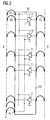
- FIG. 3shows a first embodiment of a signal amplifier with fixed high and low levels in accordance with an additional aspect of the present invention.
- FIG. 4shows a further embodiment of a signal amplifier with variable high and low signal levels in accordance with a further aspect of the present invention.
- FIG. 1shows a schematic illustration of a wafer test device in accordance with an embodiment of the present invention.
- This test devicetests chips on a wafer 1 using test signals which are supplied to these chips and are derived therefrom.
- an adapter device (“space transformer”) 2is provided which forms a needle or contact stud card.
- the test head 4contains a probe card 3 , which has a probe interface to the teste.
- the driver and receiver chips 5 , 6may be provided for signal amplification on the probe interface to the tester.
- high-performance test devicesinvolve the tester (not shown) also routing “fly-by” signals to fly-by connection points 9 , which are not actual test signals for testing the chips on the wafer 1 , but rather used for signal conditioning and timing calibration for the test signals in the tester.
- the lines carrying these fly-by signalsare denoted by 8 in FIG. 1 .
- the test devicecomprises an “interposer” 10 which mechanically and thermally decouples the probe card 3 , with its interface to the tester, and the needles or contact studs on the needle or contact stud card 2 , which are mounted on a ceramic element.
- This interposer 10comprises a printed circuit board, plated-through holes and contact pins on both sides.
- the signal amplifiers employed by the inventionare now placed on this interposer 10 , which means that they are therefore situated in substantially direct proximity to the needles.
- FIG. 2schematically shows a preferred exemplary embodiment of an interposer 10 (forming an active part) which contains the inventive signal amplifier 11 .
- the interposer 10contains a printed circuit board 101 and contact pins 13 , 14 , 15 on both sides, said contact pins making contact with the probe card 3 on one side and making contact with the needle or contact stud card 2 on the other side.
- At least one signal amplifier 11is set up such that it amplifies the respective signal received from the wafer 1 or transmitted to the wafer ( 1 ) using stipulated high and low levels.
- FIG. 2shows another embodiment, in which the signal amplifiers 11 are set up such that they amplify the respective signal which is received from the wafer 1 or transmitted to the wafer 1 using variable high and/or low signal levels.
- the interposer 10has additional pins 14 and 15 which can be used for externally supplying, i.e. from the tester, a high and a low signal level, respectively.
- the signal amplifiers 11may also each be supplied with different signal levels, which requires additional pins 14 , 15 .
- the signal amplifiers 11 on the interposer 10preferably form digital signal amplifiers in the form of a buffer.
- FIG. 3shows a circuit diagram of an ordinary digital signal amplifier 111 formed from two series-connected CMOS inverters 111 a and 111 b.
- the input signal ON supplied to this digital signal amplifier 111is amplified using fixed high and low levels and is output as an output signal OFF.
- FIG. 4shows a second embodiment of a digital signal amplifier 112 which comprises two MOS transfer gates 112 a and 112 b connected in parallel with one another.
- the transfer gate 112 a at the top in FIG. 4is supplied with the respective desired high level and the transfer gate 112 b shown at the bottom is supplied with the respective desired low level, while the inputs of both transfer gates are respectively supplied with the true and complementary input signals ⁇ , ⁇ overscore ( ⁇ ) ⁇ .
- the circuit described above and shown in the figuresmakes it possible to retrofit passive interfaces in test devices with active, preferably digital signal amplification. This makes it possible to suppress interference and signal distortions which have arisen in the signal path.
- the inexpensive alternative proposed by the inventionmay thus be used to avoid cost-intensive optimization of the hardware in the test device.
Landscapes
- Engineering & Computer Science (AREA)
- General Engineering & Computer Science (AREA)
- Physics & Mathematics (AREA)
- General Physics & Mathematics (AREA)
- Testing Or Measuring Of Semiconductors Or The Like (AREA)
Abstract
Description
- This application claims priority under 35 USC § 119 to German Application No. DE 103 55 296.0, filed on Nov. 27, 2003, and entitled “Test Device for Wafer Testing Digital Semiconductor Circuits,” the entire contents of which are hereby incorporated by reference.
- The present invention relates to a test device for testing digital semiconductor circuits at wafer level. More particularly, the present invention relates to a test device having a probe card which sends/receives digital test signals to/from a test head and distributes signal channels carrying test signals to a respective location on the wafer via an interposer, which has a printed circuit board with contact pins on both sides, and a needle or contact stud card.
- As the performance of integrated circuits particularly memory chips, rises the demands on testing also increase. At operating frequencies in the range of 500 MHz to 1 GHz, effects come to the foreground which were previously negligible for low-frequency signals. Particularly in the case of the “wafer test”, in which a test device is used to test signals directly from chips on the wafer. The problem of parasitic effects due to relatively long signal paths in comparison with a test housing of the chips need to be overcome.
- Another disadvantage is the use of needles or other resilient probe contacts giving rise to intense reciprocal effects as a result of the very short distance between the two sides in the region of the needle arrangement. These reciprocal effects can influence or interfere with the signals. Particularly in the case of digital signals with a low voltage amplitude, the signal influencing or crosstalk limits the maximum signal frequency which can be used and the input and output data windows. In the case of analog signals, the signal-to-noise ratio and hence the measurement resolution and sensitivity of the system are reduced.
- Increased coupling of capacitive or inductive type reduces the yield during the wafer test and limits the testability of critical parameters.
- The conventional contact technology attenuates the amplitude of the signal on the basis of frequency. Reflections cause ripples in the signal profile which can result in erroneous evaluation.
- To date, the parasitic effects have been reduced by using materials and design rules which differ from standard manufacturing practice of the probe cards. This has resulted in a drastic price increase. High-performance probe cards are therefore between 1.5 and 3 times more expensive than corresponding cards for standard applications.
- An aspect of the invention is thus to solve the above mentioned problems inexpensively and efficiently, and the invention provides a test device which suppresses the interference and signal distortions which have arisen in the signal path to date.
- In accordance with one aspect of the invention, which specifies a test device for testing digital semiconductor circuits at wafer level, having a probe card which sends/receives digital test signals to/from a test head and distributes signal channels carrying test signals to the respective location on the wafer via an interposer, which has a printed circuit board with contact pins on both sides, and a needle or contact stud card. This test device is characterized in that all signal channels in the test device or signal channels which carry time-critical test signals in the test device contain a respective signal amplifier.
- Additionally, digital systems have the option of reamplifying the signals which arrive at and leave the probe card using extremely simple chips. To this end, a digital amplifier is switched into the signal path for each signal. If this is done, as is preferred, as close as possible to the needle or contact stud, then it is possible to eliminate a great deal of signal distortions and interference which arise and to provide the chip pin on the wafer or tester with largely interference-free signals at the probe interface.
- Since most probe cards used today contain an “interposer” which mechanically and thermally decouples the probe card having the interface to the tester and the needles mounted on a ceramic element, the inventive signal amplifiers are preferably mounted on the printed circuit board of the interposer. The existing interposer is thus replaced by an active circuit arrangement which contains an amplification circuit at least for every time-critical signal channel or for all signal channels. The received or transmitted signal is thus reamplified after passing through the probe card and is purged of interfering signal influences. One advantage is the simple implementation in existing test systems without the need to change the basic design of the contact system, or in other words, allowing the ability to retrofit existing systems with the active circuit arrangement in accordance with an embodiment of the present invention. A further advantage is the significant cost reduction, since the use of the active elements allows the rest of the system to be produced in an inexpensive form.
- There are a number of options for implementing the signal amplification: if testing is conducive to purely digital conversion of the input/output signals, then a two-stage logic inversion element (buffer) can undertake the signal amplification. If, on the other hand, the test requires a particular signal level which differs from the supply voltage VDD for the high level and ground for the low level, for example, the invention provides an amplifier circuit having variable high and/or low levels. In this context, it should be mentioned that it is not absolutely necessary for all signal amplification elements to be implemented with variable high and/or low signal levels.
- The above and still further aspects, features and advantages of the present invention will become apparent upon consideration of the following definitions, descriptions and descriptive figures of specific embodiments thereof wherein like reference numerals in the various figures are utilized to designate like components. While these descriptions go into specific details of the invention, it should be understood that variations may and do exist and would be apparent to those skilled in the art based on the descriptions herein.
- A basic arrangement and exemplary embodiments of a test device based on the invention are described below with reference to the drawings. In the FIGs. of the drawing, specifically:
FIG. 1 schematically illustrates a basic arrangement of a test device in accordance with an aspect of the present invention;FIG. 2 schematically illustrates an interposer equipped with the inventive signal amplifiers as a preferred exemplary embodiment of the invention;FIG. 3 shows a first embodiment of a signal amplifier with fixed high and low levels in accordance with an additional aspect of the present invention; andFIG. 4 shows a further embodiment of a signal amplifier with variable high and low signal levels in accordance with a further aspect of the present invention.FIG. 1 shows a schematic illustration of a wafer test device in accordance with an embodiment of the present invention. This test device tests chips on awafer 1 using test signals which are supplied to these chips and are derived therefrom. In order to distribute these signals physically over a number of chips on thewafer 1, an adapter device (“space transformer”)2 is provided which forms a needle or contact stud card. The test head4 contains aprobe card 3, which has a probe interface to the teste. The driver and receiver chips5,6 may be provided for signal amplification on the probe interface to the tester.- In this context, it should be mentioned that high-performance test devices involve the tester (not shown) also routing “fly-by” signals to fly-by
connection points 9, which are not actual test signals for testing the chips on thewafer 1, but rather used for signal conditioning and timing calibration for the test signals in the tester. The lines carrying these fly-by signals are denoted by8 inFIG. 1 . - In addition, between the needle or
contact stud card 2 and theprobe card 3, the test device comprises an “interposer”10 which mechanically and thermally decouples theprobe card 3, with its interface to the tester, and the needles or contact studs on the needle orcontact stud card 2, which are mounted on a ceramic element. Thisinterposer 10 comprises a printed circuit board, plated-through holes and contact pins on both sides. - In the case of the preferred exemplary embodiment, the signal amplifiers employed by the invention are now placed on this
interposer 10, which means that they are therefore situated in substantially direct proximity to the needles. FIG. 2 schematically shows a preferred exemplary embodiment of an interposer10 (forming an active part) which contains theinventive signal amplifier 11. As mentioned, theinterposer 10 contains a printedcircuit board 101 andcontact pins probe card 3 on one side and making contact with the needle or contactstud card 2 on the other side.- In accordance with one embodiment, at least one
signal amplifier 11 is set up such that it amplifies the respective signal received from thewafer 1 or transmitted to the wafer (1) using stipulated high and low levels. - By contrast,
FIG. 2 shows another embodiment, in which thesignal amplifiers 11 are set up such that they amplify the respective signal which is received from thewafer 1 or transmitted to thewafer 1 using variable high and/or low signal levels. To this end, theinterposer 10 hasadditional pins FIG. 2 , thesignal amplifiers 11 may also each be supplied with different signal levels, which requiresadditional pins - As previously mentioned, the signal amplifiers11 on the
interposer 10 preferably form digital signal amplifiers in the form of a buffer. FIG. 3 shows a circuit diagram of an ordinarydigital signal amplifier 111 formed from two series-connectedCMOS inverters digital signal amplifier 111 is amplified using fixed high and low levels and is output as an output signal OFF.FIG. 4 shows a second embodiment of adigital signal amplifier 112 which comprises twoMOS transfer gates transfer gate 112aat the top inFIG. 4 is supplied with the respective desired high level and thetransfer gate 112bshown at the bottom is supplied with the respective desired low level, while the inputs of both transfer gates are respectively supplied with the true and complementary input signals φ, {overscore (φ)}.- The circuit described above and shown in the figures makes it possible to retrofit passive interfaces in test devices with active, preferably digital signal amplification. This makes it possible to suppress interference and signal distortions which have arisen in the signal path. The inexpensive alternative proposed by the invention may thus be used to avoid cost-intensive optimization of the hardware in the test device.
- While the invention has been described in detail and with reference to specific embodiments thereof, it will be apparent to one skilled in the art that various changes and modifications can be made therein without departing from the spirit and scope thereof. Accordingly, it is intended that the present invention covers the modifications and variations of this invention provided they come within the scope of the appended claims and their equivalents.
- 1 Wafer
- 2 Needle or contact stud card
- 3 Probe card
- 4 Test head
- 5,6 Receiver and driver in the probe interface
- 8 Fly-by signals
- 9 Fly-by connection points
- 10 Interposer
- 11 Signal amplifier
- 13 Contact pins
- 14 High-level and low-level contact pins
- 111 First embodiment of the digital signal amplifier
- 111aFirst inverter
- 112bSecond inverter
- 112 Second embodiment of the digital signal amplifier
- 112aFirst transfer gate
- 112bSecond transfer gate
- φ, {overscore (φ)} True and complementary input signal
Claims (8)
Applications Claiming Priority (2)
| Application Number | Priority Date | Filing Date | Title |
|---|---|---|---|
| DE10355296.0 | 2003-11-27 | ||
| DE10355296ADE10355296B3 (en) | 2003-11-27 | 2003-11-27 | Testing device for wafer testing of digital semiconductor circuits with signal amplifiers inserted in test signal channels for eliminating signal attentuation and noise |
Publications (2)
| Publication Number | Publication Date |
|---|---|
| US20050162176A1true US20050162176A1 (en) | 2005-07-28 |
| US7180313B2 US7180313B2 (en) | 2007-02-20 |
Family
ID=34559738
Family Applications (1)
| Application Number | Title | Priority Date | Filing Date |
|---|---|---|---|
| US10/995,111Expired - Fee RelatedUS7180313B2 (en) | 2003-11-27 | 2004-11-24 | Test device for wafer testing digital semiconductor circuits |
Country Status (2)
| Country | Link |
|---|---|
| US (1) | US7180313B2 (en) |
| DE (1) | DE10355296B3 (en) |
Cited By (33)
| Publication number | Priority date | Publication date | Assignee | Title |
|---|---|---|---|---|
| US20120056640A1 (en)* | 2009-06-29 | 2012-03-08 | Hsio Technologies, Llc | Compliant printed circuit semiconductor tester interface |
| US8952713B1 (en)* | 2012-02-08 | 2015-02-10 | Altera Corporation | Method and apparatus for die testing |
| US9054097B2 (en) | 2009-06-02 | 2015-06-09 | Hsio Technologies, Llc | Compliant printed circuit area array semiconductor device package |
| US9076884B2 (en) | 2009-06-02 | 2015-07-07 | Hsio Technologies, Llc | Compliant printed circuit semiconductor package |
| US9093767B2 (en) | 2009-06-02 | 2015-07-28 | Hsio Technologies, Llc | High performance surface mount electrical interconnect |
| US20150212112A1 (en)* | 2014-01-24 | 2015-07-30 | Sitronix Technology Corp. | Active Probe Card |
| US9136196B2 (en) | 2009-06-02 | 2015-09-15 | Hsio Technologies, Llc | Compliant printed circuit wafer level semiconductor package |
| US9184145B2 (en) | 2009-06-02 | 2015-11-10 | Hsio Technologies, Llc | Semiconductor device package adapter |
| US9184527B2 (en) | 2009-06-02 | 2015-11-10 | Hsio Technologies, Llc | Electrical connector insulator housing |
| US9196980B2 (en) | 2009-06-02 | 2015-11-24 | Hsio Technologies, Llc | High performance surface mount electrical interconnect with external biased normal force loading |
| US9232654B2 (en) | 2009-06-02 | 2016-01-05 | Hsio Technologies, Llc | High performance electrical circuit structure |
| US9231328B2 (en) | 2009-06-02 | 2016-01-05 | Hsio Technologies, Llc | Resilient conductive electrical interconnect |
| US9276339B2 (en) | 2009-06-02 | 2016-03-01 | Hsio Technologies, Llc | Electrical interconnect IC device socket |
| US9277654B2 (en) | 2009-06-02 | 2016-03-01 | Hsio Technologies, Llc | Composite polymer-metal electrical contacts |
| US9276336B2 (en) | 2009-05-28 | 2016-03-01 | Hsio Technologies, Llc | Metalized pad to electrical contact interface |
| US9318862B2 (en) | 2009-06-02 | 2016-04-19 | Hsio Technologies, Llc | Method of making an electronic interconnect |
| US9320133B2 (en) | 2009-06-02 | 2016-04-19 | Hsio Technologies, Llc | Electrical interconnect IC device socket |
| US9320144B2 (en) | 2009-06-17 | 2016-04-19 | Hsio Technologies, Llc | Method of forming a semiconductor socket |
| US9350093B2 (en) | 2010-06-03 | 2016-05-24 | Hsio Technologies, Llc | Selective metalization of electrical connector or socket housing |
| US9414500B2 (en) | 2009-06-02 | 2016-08-09 | Hsio Technologies, Llc | Compliant printed flexible circuit |
| US9536815B2 (en) | 2009-05-28 | 2017-01-03 | Hsio Technologies, Llc | Semiconductor socket with direct selective metalization |
| US9559447B2 (en) | 2015-03-18 | 2017-01-31 | Hsio Technologies, Llc | Mechanical contact retention within an electrical connector |
| US9603249B2 (en) | 2009-06-02 | 2017-03-21 | Hsio Technologies, Llc | Direct metalization of electrical circuit structures |
| US9613841B2 (en) | 2009-06-02 | 2017-04-04 | Hsio Technologies, Llc | Area array semiconductor device package interconnect structure with optional package-to-package or flexible circuit to package connection |
| US9660368B2 (en) | 2009-05-28 | 2017-05-23 | Hsio Technologies, Llc | High performance surface mount electrical interconnect |
| US9689897B2 (en) | 2010-06-03 | 2017-06-27 | Hsio Technologies, Llc | Performance enhanced semiconductor socket |
| US9699906B2 (en) | 2009-06-02 | 2017-07-04 | Hsio Technologies, Llc | Hybrid printed circuit assembly with low density main core and embedded high density circuit regions |
| US9761520B2 (en) | 2012-07-10 | 2017-09-12 | Hsio Technologies, Llc | Method of making an electrical connector having electrodeposited terminals |
| US9930775B2 (en) | 2009-06-02 | 2018-03-27 | Hsio Technologies, Llc | Copper pillar full metal via electrical circuit structure |
| WO2018208586A1 (en)* | 2017-05-12 | 2018-11-15 | Delta V Instruments, Inc. | Wafer level burn-in system |
| US10159154B2 (en) | 2010-06-03 | 2018-12-18 | Hsio Technologies, Llc | Fusion bonded liquid crystal polymer circuit structure |
| US10506722B2 (en) | 2013-07-11 | 2019-12-10 | Hsio Technologies, Llc | Fusion bonded liquid crystal polymer electrical circuit structure |
| US10667410B2 (en) | 2013-07-11 | 2020-05-26 | Hsio Technologies, Llc | Method of making a fusion bonded circuit structure |
Families Citing this family (7)
| Publication number | Priority date | Publication date | Assignee | Title |
|---|---|---|---|---|
| DE102004057772B3 (en)* | 2004-11-30 | 2006-05-24 | Infineon Technologies Ag | Insertable calibration device for programmable tester programs transmission time point so occurrences of calibration signal edge and reference signal edge essentially coincide to compensate for signal transition time differences |
| US7262624B2 (en)* | 2004-12-21 | 2007-08-28 | Formfactor, Inc. | Bi-directional buffer for interfacing test system channel |
| WO2010147934A1 (en) | 2009-06-16 | 2010-12-23 | Hsio Technologies, Llc | Semiconductor die terminal |
| US8988093B2 (en) | 2009-06-02 | 2015-03-24 | Hsio Technologies, Llc | Bumped semiconductor wafer or die level electrical interconnect |
| WO2010141313A1 (en)* | 2009-06-02 | 2010-12-09 | Hsio Technologies, Llc | Compliant printed circuit socket diagnostic tool |
| US8912812B2 (en)* | 2009-06-02 | 2014-12-16 | Hsio Technologies, Llc | Compliant printed circuit wafer probe diagnostic tool |
| US8984748B2 (en) | 2009-06-29 | 2015-03-24 | Hsio Technologies, Llc | Singulated semiconductor device separable electrical interconnect |
Citations (13)
| Publication number | Priority date | Publication date | Assignee | Title |
|---|---|---|---|---|
| US5070297A (en)* | 1990-06-04 | 1991-12-03 | Texas Instruments Incorporated | Full wafer integrated circuit testing device |
| US5512838A (en)* | 1992-09-03 | 1996-04-30 | Hewlett-Packard Company | Probe with reduced input capacitance |
| US5583446A (en)* | 1993-04-13 | 1996-12-10 | Teratec Corporation | Electro-optically controlled measurement probe system |
| US5794175A (en)* | 1997-09-09 | 1998-08-11 | Teradyne, Inc. | Low cost, highly parallel memory tester |
| US5974662A (en)* | 1993-11-16 | 1999-11-02 | Formfactor, Inc. | Method of planarizing tips of probe elements of a probe card assembly |
| US6392296B1 (en)* | 1998-08-31 | 2002-05-21 | Micron Technology, Inc. | Silicon interposer with optical connections |
| US6462528B1 (en)* | 2000-05-23 | 2002-10-08 | Tektronix, Inc. | Method and apparatus for probing a conductor of an array of closely-spaced conductors |
| US20020153876A1 (en)* | 2001-04-09 | 2002-10-24 | De Jong Franciscus Gerardus Maria | Integrated circuit with power supply test interface |
| US6476598B2 (en)* | 1995-04-17 | 2002-11-05 | Mitsubishi Denki Kabushiki Kaisha | Ringing preventive circuit, device under test board, pin electronics card, and semiconductor device |
| US6483328B1 (en)* | 1995-11-09 | 2002-11-19 | Formfactor, Inc. | Probe card for probing wafers with raised contact elements |
| US20040075459A1 (en)* | 2000-01-18 | 2004-04-22 | Formfactor, Inc. | Predictive, adaptive power supply for an integrated circuit under test |
| US20040174177A1 (en)* | 2000-08-21 | 2004-09-09 | Tokyo Electron Limited | Inspection method and inspection apparatus |
| US6924653B2 (en)* | 2002-08-26 | 2005-08-02 | Micron Technology, Inc. | Selectively configurable microelectronic probes |
- 2003
- 2003-11-27DEDE10355296Apatent/DE10355296B3/ennot_activeExpired - Fee Related
- 2004
- 2004-11-24USUS10/995,111patent/US7180313B2/ennot_activeExpired - Fee Related
Patent Citations (15)
| Publication number | Priority date | Publication date | Assignee | Title |
|---|---|---|---|---|
| US5070297A (en)* | 1990-06-04 | 1991-12-03 | Texas Instruments Incorporated | Full wafer integrated circuit testing device |
| US5512838A (en)* | 1992-09-03 | 1996-04-30 | Hewlett-Packard Company | Probe with reduced input capacitance |
| US5583446A (en)* | 1993-04-13 | 1996-12-10 | Teratec Corporation | Electro-optically controlled measurement probe system |
| US5974662A (en)* | 1993-11-16 | 1999-11-02 | Formfactor, Inc. | Method of planarizing tips of probe elements of a probe card assembly |
| US6476598B2 (en)* | 1995-04-17 | 2002-11-05 | Mitsubishi Denki Kabushiki Kaisha | Ringing preventive circuit, device under test board, pin electronics card, and semiconductor device |
| US6937037B2 (en)* | 1995-11-09 | 2005-08-30 | Formfactor, Et Al. | Probe card assembly for contacting a device with raised contact elements |
| US6483328B1 (en)* | 1995-11-09 | 2002-11-19 | Formfactor, Inc. | Probe card for probing wafers with raised contact elements |
| US5794175A (en)* | 1997-09-09 | 1998-08-11 | Teradyne, Inc. | Low cost, highly parallel memory tester |
| US6392296B1 (en)* | 1998-08-31 | 2002-05-21 | Micron Technology, Inc. | Silicon interposer with optical connections |
| US20040075459A1 (en)* | 2000-01-18 | 2004-04-22 | Formfactor, Inc. | Predictive, adaptive power supply for an integrated circuit under test |
| US6462528B1 (en)* | 2000-05-23 | 2002-10-08 | Tektronix, Inc. | Method and apparatus for probing a conductor of an array of closely-spaced conductors |
| US20040174177A1 (en)* | 2000-08-21 | 2004-09-09 | Tokyo Electron Limited | Inspection method and inspection apparatus |
| US20020153876A1 (en)* | 2001-04-09 | 2002-10-24 | De Jong Franciscus Gerardus Maria | Integrated circuit with power supply test interface |
| US6812690B2 (en)* | 2001-04-09 | 2004-11-02 | Koninklijke Philips Electronics N.V. | Integrated circuit with power supply test interface |
| US6924653B2 (en)* | 2002-08-26 | 2005-08-02 | Micron Technology, Inc. | Selectively configurable microelectronic probes |
Cited By (40)
| Publication number | Priority date | Publication date | Assignee | Title |
|---|---|---|---|---|
| US9276336B2 (en) | 2009-05-28 | 2016-03-01 | Hsio Technologies, Llc | Metalized pad to electrical contact interface |
| US9660368B2 (en) | 2009-05-28 | 2017-05-23 | Hsio Technologies, Llc | High performance surface mount electrical interconnect |
| US9536815B2 (en) | 2009-05-28 | 2017-01-03 | Hsio Technologies, Llc | Semiconductor socket with direct selective metalization |
| US9277654B2 (en) | 2009-06-02 | 2016-03-01 | Hsio Technologies, Llc | Composite polymer-metal electrical contacts |
| US9318862B2 (en) | 2009-06-02 | 2016-04-19 | Hsio Technologies, Llc | Method of making an electronic interconnect |
| US9093767B2 (en) | 2009-06-02 | 2015-07-28 | Hsio Technologies, Llc | High performance surface mount electrical interconnect |
| US10609819B2 (en) | 2009-06-02 | 2020-03-31 | Hsio Technologies, Llc | Hybrid printed circuit assembly with low density main core and embedded high density circuit regions |
| US9136196B2 (en) | 2009-06-02 | 2015-09-15 | Hsio Technologies, Llc | Compliant printed circuit wafer level semiconductor package |
| US9184145B2 (en) | 2009-06-02 | 2015-11-10 | Hsio Technologies, Llc | Semiconductor device package adapter |
| US9184527B2 (en) | 2009-06-02 | 2015-11-10 | Hsio Technologies, Llc | Electrical connector insulator housing |
| US9196980B2 (en) | 2009-06-02 | 2015-11-24 | Hsio Technologies, Llc | High performance surface mount electrical interconnect with external biased normal force loading |
| US9232654B2 (en) | 2009-06-02 | 2016-01-05 | Hsio Technologies, Llc | High performance electrical circuit structure |
| US9231328B2 (en) | 2009-06-02 | 2016-01-05 | Hsio Technologies, Llc | Resilient conductive electrical interconnect |
| US9276339B2 (en) | 2009-06-02 | 2016-03-01 | Hsio Technologies, Llc | Electrical interconnect IC device socket |
| US9613841B2 (en) | 2009-06-02 | 2017-04-04 | Hsio Technologies, Llc | Area array semiconductor device package interconnect structure with optional package-to-package or flexible circuit to package connection |
| US9054097B2 (en) | 2009-06-02 | 2015-06-09 | Hsio Technologies, Llc | Compliant printed circuit area array semiconductor device package |
| US9076884B2 (en) | 2009-06-02 | 2015-07-07 | Hsio Technologies, Llc | Compliant printed circuit semiconductor package |
| US9320133B2 (en) | 2009-06-02 | 2016-04-19 | Hsio Technologies, Llc | Electrical interconnect IC device socket |
| US9603249B2 (en) | 2009-06-02 | 2017-03-21 | Hsio Technologies, Llc | Direct metalization of electrical circuit structures |
| US9699906B2 (en) | 2009-06-02 | 2017-07-04 | Hsio Technologies, Llc | Hybrid printed circuit assembly with low density main core and embedded high density circuit regions |
| US9930775B2 (en) | 2009-06-02 | 2018-03-27 | Hsio Technologies, Llc | Copper pillar full metal via electrical circuit structure |
| US9414500B2 (en) | 2009-06-02 | 2016-08-09 | Hsio Technologies, Llc | Compliant printed flexible circuit |
| US9320144B2 (en) | 2009-06-17 | 2016-04-19 | Hsio Technologies, Llc | Method of forming a semiconductor socket |
| US20120056640A1 (en)* | 2009-06-29 | 2012-03-08 | Hsio Technologies, Llc | Compliant printed circuit semiconductor tester interface |
| US8981809B2 (en)* | 2009-06-29 | 2015-03-17 | Hsio Technologies, Llc | Compliant printed circuit semiconductor tester interface |
| US9350093B2 (en) | 2010-06-03 | 2016-05-24 | Hsio Technologies, Llc | Selective metalization of electrical connector or socket housing |
| US9689897B2 (en) | 2010-06-03 | 2017-06-27 | Hsio Technologies, Llc | Performance enhanced semiconductor socket |
| US10159154B2 (en) | 2010-06-03 | 2018-12-18 | Hsio Technologies, Llc | Fusion bonded liquid crystal polymer circuit structure |
| US9350124B2 (en) | 2010-12-01 | 2016-05-24 | Hsio Technologies, Llc | High speed circuit assembly with integral terminal and mating bias loading electrical connector assembly |
| US8952713B1 (en)* | 2012-02-08 | 2015-02-10 | Altera Corporation | Method and apparatus for die testing |
| US9761520B2 (en) | 2012-07-10 | 2017-09-12 | Hsio Technologies, Llc | Method of making an electrical connector having electrodeposited terminals |
| US10453789B2 (en) | 2012-07-10 | 2019-10-22 | Hsio Technologies, Llc | Electrodeposited contact terminal for use as an electrical connector or semiconductor packaging substrate |
| US10506722B2 (en) | 2013-07-11 | 2019-12-10 | Hsio Technologies, Llc | Fusion bonded liquid crystal polymer electrical circuit structure |
| US10667410B2 (en) | 2013-07-11 | 2020-05-26 | Hsio Technologies, Llc | Method of making a fusion bonded circuit structure |
| US9506974B2 (en)* | 2014-01-24 | 2016-11-29 | Sitronix Technology Corp. | Active probe card |
| US20150212112A1 (en)* | 2014-01-24 | 2015-07-30 | Sitronix Technology Corp. | Active Probe Card |
| US9559447B2 (en) | 2015-03-18 | 2017-01-31 | Hsio Technologies, Llc | Mechanical contact retention within an electrical connector |
| US9755335B2 (en) | 2015-03-18 | 2017-09-05 | Hsio Technologies, Llc | Low profile electrical interconnect with fusion bonded contact retention and solder wick reduction |
| WO2018208586A1 (en)* | 2017-05-12 | 2018-11-15 | Delta V Instruments, Inc. | Wafer level burn-in system |
| US10267845B2 (en)* | 2017-05-12 | 2019-04-23 | Delta V Instruments, Inc. | Wafer level burn-in system |
Also Published As
| Publication number | Publication date |
|---|---|
| US7180313B2 (en) | 2007-02-20 |
| DE10355296B3 (en) | 2005-06-09 |
Similar Documents
| Publication | Publication Date | Title |
|---|---|---|
| US7180313B2 (en) | Test device for wafer testing digital semiconductor circuits | |
| US7471220B2 (en) | Electronic test circuit for an integrated circuit and methods for testing the driver strength and for testing the input sensitivity of a receiver of the integrated circuit | |
| US7772828B2 (en) | Automatic test equipment capable of high speed test | |
| JP5735856B2 (en) | Semiconductor chip and semiconductor chip inspection method | |
| US20060111861A1 (en) | System and method for calibrating signal paths connecting a device under test to a test system | |
| US7250770B2 (en) | Semiconductor integrated circuit device | |
| JP2760284B2 (en) | Semiconductor integrated circuit device | |
| US6292415B1 (en) | Enhancements in testing devices on burn-in boards | |
| US6849956B2 (en) | Semiconductor integrated circuit with shortened pad pitch | |
| US6356095B1 (en) | Semiconductor integrated circuit | |
| US9432020B2 (en) | Communication cell for an integrated circuit operating in contact and contactless mode, electronic chip comprising the communication cell, electronic system including the chip, and test apparatus | |
| US8773162B2 (en) | Communication cell for an integrated circuit, chip comprising said communication cell, electronic system including the chip, and test apparatus | |
| US7812625B2 (en) | Chip test apparatus and probe card circuit | |
| US20020199139A1 (en) | Test configuration for a parallel functional testing of semiconductor memory modules and test method | |
| US6851079B1 (en) | Jtag test access port controller used to control input/output pad functionality | |
| US20240175920A1 (en) | Benchmark circuit on a semiconductor wafer and method for operating the same | |
| US5949240A (en) | Test connecting device including testkey and probe card for use in the testing of integrated circuits | |
| US7251772B2 (en) | Circuit arrangement having a number of integrated circuit components on a carrier substrate and method for testing a circuit arrangement of this type | |
| US7336066B2 (en) | Reduced pin count test method and apparatus | |
| US7489153B2 (en) | Semiconductor memory device | |
| US6714034B2 (en) | Integrated circuit testing apparatus having stable ground reference | |
| US10559374B2 (en) | Circuit topology of memory chips with embedded function test pattern generation module connected to normal access port physical layer | |
| US20050077600A1 (en) | Semiconductor device | |
| US20090091345A1 (en) | Structure for providing a duplicate test signal of an output signal under test in an integrated circuit | |
| US7663391B2 (en) | Test system and method for reducing test signal loss for integrated circuits |
Legal Events
| Date | Code | Title | Description |
|---|---|---|---|
| AS | Assignment | Owner name:INFINEON TECHNOLOGIES AG, GERMANY Free format text:ASSIGNMENT OF ASSIGNORS INTEREST;ASSIGNOR:BUCKSCH, THORSTEN;REEL/FRAME:015539/0246 Effective date:20041206 | |
| AS | Assignment | Owner name:QIMONDA AG, GERMANY Free format text:ASSIGNMENT OF ASSIGNORS INTEREST;ASSIGNOR:INFINEON TECHNOLOGIES AG;REEL/FRAME:023853/0001 Effective date:20060425 | |
| FPAY | Fee payment | Year of fee payment:4 | |
| FPAY | Fee payment | Year of fee payment:8 | |
| AS | Assignment | Owner name:INFINEON TECHNOLOGIES AG, GERMANY Free format text:ASSIGNMENT OF ASSIGNORS INTEREST;ASSIGNOR:QIMONDA AG;REEL/FRAME:035623/0001 Effective date:20141009 | |
| AS | Assignment | Owner name:POLARIS INNOVATIONS LIMITED, IRELAND Free format text:ASSIGNMENT OF ASSIGNORS INTEREST;ASSIGNOR:INFINEON TECHNOLOGIES AG;REEL/FRAME:036888/0745 Effective date:20150708 | |
| FEPP | Fee payment procedure | Free format text:MAINTENANCE FEE REMINDER MAILED (ORIGINAL EVENT CODE: REM.); ENTITY STATUS OF PATENT OWNER: LARGE ENTITY | |
| LAPS | Lapse for failure to pay maintenance fees | Free format text:PATENT EXPIRED FOR FAILURE TO PAY MAINTENANCE FEES (ORIGINAL EVENT CODE: EXP.); ENTITY STATUS OF PATENT OWNER: LARGE ENTITY | |
| STCH | Information on status: patent discontinuation | Free format text:PATENT EXPIRED DUE TO NONPAYMENT OF MAINTENANCE FEES UNDER 37 CFR 1.362 | |
| FP | Lapsed due to failure to pay maintenance fee | Effective date:20190220 |