US20050158985A1 - Copper recess process with application to selective capping and electroless plating - Google Patents
Copper recess process with application to selective capping and electroless platingDownload PDFInfo
- Publication number
- US20050158985A1 US20050158985A1US11/058,783US5878305AUS2005158985A1US 20050158985 A1US20050158985 A1US 20050158985A1US 5878305 AUS5878305 AUS 5878305AUS 2005158985 A1US2005158985 A1US 2005158985A1
- Authority
- US
- United States
- Prior art keywords
- layer
- depositing
- cap
- metal features
- metal
- Prior art date
- Legal status (The legal status is an assumption and is not a legal conclusion. Google has not performed a legal analysis and makes no representation as to the accuracy of the status listed.)
- Granted
Links
- 238000000034methodMethods0.000titleclaimsdescription36
- 238000007772electroless platingMethods0.000titleclaimsdescription4
- RYGMFSIKBFXOCR-UHFFFAOYSA-NCopperChemical compound[Cu]RYGMFSIKBFXOCR-UHFFFAOYSA-N0.000titledescription7
- 229910052802copperInorganic materials0.000titledescription7
- 239000010949copperSubstances0.000titledescription7
- 230000004888barrier functionEffects0.000claimsdescription34
- 229910052751metalInorganic materials0.000claimsdescription26
- 239000002184metalSubstances0.000claimsdescription26
- 239000000463materialSubstances0.000claimsdescription23
- 239000003989dielectric materialSubstances0.000claimsdescription15
- 238000000151depositionMethods0.000claimsdescription13
- 239000012212insulatorSubstances0.000claimsdescription13
- 239000007769metal materialSubstances0.000claimsdescription3
- 239000000758substrateSubstances0.000abstractdescription6
- 239000010410layerSubstances0.000description68
- 239000004020conductorSubstances0.000description20
- 238000010586diagramMethods0.000description12
- 238000012545processingMethods0.000description12
- VYPSYNLAJGMNEJ-UHFFFAOYSA-NSilicium dioxideChemical compoundO=[Si]=OVYPSYNLAJGMNEJ-UHFFFAOYSA-N0.000description8
- 238000013508migrationMethods0.000description8
- 230000005012migrationEffects0.000description8
- 238000001020plasma etchingMethods0.000description7
- KDLHZDBZIXYQEI-UHFFFAOYSA-NPalladiumChemical compound[Pd]KDLHZDBZIXYQEI-UHFFFAOYSA-N0.000description6
- 239000000126substanceSubstances0.000description6
- 230000015572biosynthetic processEffects0.000description5
- 238000009792diffusion processMethods0.000description5
- 229910052681coesiteInorganic materials0.000description4
- 229910052906cristobaliteInorganic materials0.000description4
- 238000010899nucleationMethods0.000description4
- 239000000377silicon dioxideSubstances0.000description4
- 229910052682stishoviteInorganic materials0.000description4
- 229910052905tridymiteInorganic materials0.000description4
- QVGXLLKOCUKJST-UHFFFAOYSA-Natomic oxygenChemical compound[O]QVGXLLKOCUKJST-UHFFFAOYSA-N0.000description3
- 230000008021depositionEffects0.000description3
- 229910052760oxygenInorganic materials0.000description3
- 239000001301oxygenSubstances0.000description3
- 238000005498polishingMethods0.000description3
- 238000007517polishing processMethods0.000description3
- HBMJWWWQQXIZIP-UHFFFAOYSA-Nsilicon carbideChemical compound[Si+]#[C-]HBMJWWWQQXIZIP-UHFFFAOYSA-N0.000description3
- 229910010271silicon carbideInorganic materials0.000description3
- 229910052721tungstenInorganic materials0.000description3
- IJGRMHOSHXDMSA-UHFFFAOYSA-NAtomic nitrogenChemical compoundN#NIJGRMHOSHXDMSA-UHFFFAOYSA-N0.000description2
- PXHVJJICTQNCMI-UHFFFAOYSA-NNickelChemical compound[Ni]PXHVJJICTQNCMI-UHFFFAOYSA-N0.000description2
- ATJFFYVFTNAWJD-UHFFFAOYSA-NTinChemical compound[Sn]ATJFFYVFTNAWJD-UHFFFAOYSA-N0.000description2
- 238000004140cleaningMethods0.000description2
- 238000005260corrosionMethods0.000description2
- 230000007797corrosionEffects0.000description2
- 238000013461designMethods0.000description2
- BASFCYQUMIYNBI-UHFFFAOYSA-NplatinumChemical compound[Pt]BASFCYQUMIYNBI-UHFFFAOYSA-N0.000description2
- 235000012239silicon dioxideNutrition0.000description2
- 239000002002slurrySubstances0.000description2
- 229910052715tantalumInorganic materials0.000description2
- 229910052718tinInorganic materials0.000description2
- WFKWXMTUELFFGS-UHFFFAOYSA-NtungstenChemical compound[W]WFKWXMTUELFFGS-UHFFFAOYSA-N0.000description2
- 239000010937tungstenSubstances0.000description2
- ZOXJGFHDIHLPTG-UHFFFAOYSA-NBoronChemical compound[B]ZOXJGFHDIHLPTG-UHFFFAOYSA-N0.000description1
- OYPRJOBELJOOCE-UHFFFAOYSA-NCalciumChemical compound[Ca]OYPRJOBELJOOCE-UHFFFAOYSA-N0.000description1
- 244000132059Carica parvifloraSpecies0.000description1
- 235000014653Carica parvifloraNutrition0.000description1
- VYZAMTAEIAYCRO-UHFFFAOYSA-NChromiumChemical compound[Cr]VYZAMTAEIAYCRO-UHFFFAOYSA-N0.000description1
- UFHFLCQGNIYNRP-UHFFFAOYSA-NHydrogenChemical compound[H][H]UFHFLCQGNIYNRP-UHFFFAOYSA-N0.000description1
- ZOKXTWBITQBERF-UHFFFAOYSA-NMolybdenumChemical compound[Mo]ZOKXTWBITQBERF-UHFFFAOYSA-N0.000description1
- KJTLSVCANCCWHF-UHFFFAOYSA-NRutheniumChemical compound[Ru]KJTLSVCANCCWHF-UHFFFAOYSA-N0.000description1
- 229910052581Si3N4Inorganic materials0.000description1
- 229910004166TaNInorganic materials0.000description1
- 229910008482TiSiNInorganic materials0.000description1
- RTAQQCXQSZGOHL-UHFFFAOYSA-NTitaniumChemical compound[Ti]RTAQQCXQSZGOHL-UHFFFAOYSA-N0.000description1
- HCHKCACWOHOZIP-UHFFFAOYSA-NZincChemical compound[Zn]HCHKCACWOHOZIP-UHFFFAOYSA-N0.000description1
- 230000002378acidificating effectEffects0.000description1
- 229910052787antimonyInorganic materials0.000description1
- WATWJIUSRGPENY-UHFFFAOYSA-Nantimony atomChemical compound[Sb]WATWJIUSRGPENY-UHFFFAOYSA-N0.000description1
- 229910052790berylliumInorganic materials0.000description1
- ATBAMAFKBVZNFJ-UHFFFAOYSA-Nberyllium atomChemical compound[Be]ATBAMAFKBVZNFJ-UHFFFAOYSA-N0.000description1
- 229910052796boronInorganic materials0.000description1
- 229910052793cadmiumInorganic materials0.000description1
- BDOSMKKIYDKNTQ-UHFFFAOYSA-Ncadmium atomChemical compound[Cd]BDOSMKKIYDKNTQ-UHFFFAOYSA-N0.000description1
- 229910052791calciumInorganic materials0.000description1
- 239000011575calciumSubstances0.000description1
- 229910052804chromiumInorganic materials0.000description1
- 239000011651chromiumSubstances0.000description1
- 229910017052cobaltInorganic materials0.000description1
- 239000010941cobaltSubstances0.000description1
- GUTLYIVDDKVIGB-UHFFFAOYSA-Ncobalt atomChemical compound[Co]GUTLYIVDDKVIGB-UHFFFAOYSA-N0.000description1
- 230000001419dependent effectEffects0.000description1
- 239000010432diamondSubstances0.000description1
- 230000005684electric fieldEffects0.000description1
- 239000007789gasSubstances0.000description1
- 239000011521glassSubstances0.000description1
- 229910052735hafniumInorganic materials0.000description1
- VBJZVLUMGGDVMO-UHFFFAOYSA-Nhafnium atomChemical compound[Hf]VBJZVLUMGGDVMO-UHFFFAOYSA-N0.000description1
- BHEPBYXIRTUNPN-UHFFFAOYSA-Nhydridophosphorus(.) (triplet)Chemical compound[PH]BHEPBYXIRTUNPN-UHFFFAOYSA-N0.000description1
- 239000001257hydrogenSubstances0.000description1
- 229910052739hydrogenInorganic materials0.000description1
- 229910052738indiumInorganic materials0.000description1
- APFVFJFRJDLVQX-UHFFFAOYSA-Nindium atomChemical compound[In]APFVFJFRJDLVQX-UHFFFAOYSA-N0.000description1
- 230000002401inhibitory effectEffects0.000description1
- 239000011810insulating materialSubstances0.000description1
- QRXWMOHMRWLFEY-UHFFFAOYSA-NisoniazideChemical compoundNNC(=O)C1=CC=NC=C1QRXWMOHMRWLFEY-UHFFFAOYSA-N0.000description1
- 239000002346layers by functionSubstances0.000description1
- 150000002739metalsChemical class0.000description1
- 238000012986modificationMethods0.000description1
- 230000004048modificationEffects0.000description1
- 229910052750molybdenumInorganic materials0.000description1
- 239000011733molybdenumSubstances0.000description1
- 229910052759nickelInorganic materials0.000description1
- 229910052757nitrogenInorganic materials0.000description1
- 230000001590oxidative effectEffects0.000description1
- -1oxidesInorganic materials0.000description1
- 229910052763palladiumInorganic materials0.000description1
- 238000005240physical vapour depositionMethods0.000description1
- 238000009832plasma treatmentMethods0.000description1
- 229910052697platinumInorganic materials0.000description1
- 229910052703rhodiumInorganic materials0.000description1
- 239000010948rhodiumSubstances0.000description1
- MHOVAHRLVXNVSD-UHFFFAOYSA-Nrhodium atomChemical compound[Rh]MHOVAHRLVXNVSD-UHFFFAOYSA-N0.000description1
- 229910052707rutheniumInorganic materials0.000description1
- 239000005368silicate glassSubstances0.000description1
- GUVRBAGPIYLISA-UHFFFAOYSA-Ntantalum atomChemical compound[Ta]GUVRBAGPIYLISA-UHFFFAOYSA-N0.000description1
- 229910052719titaniumInorganic materials0.000description1
- 239000010936titaniumSubstances0.000description1
- 238000007740vapor depositionMethods0.000description1
- 229910052725zincInorganic materials0.000description1
- 239000011701zincSubstances0.000description1
Images


Classifications
- H—ELECTRICITY
- H01—ELECTRIC ELEMENTS
- H01L—SEMICONDUCTOR DEVICES NOT COVERED BY CLASS H10
- H01L21/00—Processes or apparatus adapted for the manufacture or treatment of semiconductor or solid state devices or of parts thereof
- H01L21/70—Manufacture or treatment of devices consisting of a plurality of solid state components formed in or on a common substrate or of parts thereof; Manufacture of integrated circuit devices or of parts thereof
- H01L21/71—Manufacture of specific parts of devices defined in group H01L21/70
- H01L21/768—Applying interconnections to be used for carrying current between separate components within a device comprising conductors and dielectrics
- H01L21/76838—Applying interconnections to be used for carrying current between separate components within a device comprising conductors and dielectrics characterised by the formation and the after-treatment of the conductors
- H01L21/76841—Barrier, adhesion or liner layers
- H01L21/76843—Barrier, adhesion or liner layers formed in openings in a dielectric
- H01L21/76849—Barrier, adhesion or liner layers formed in openings in a dielectric the layer being positioned on top of the main fill metal
- H—ELECTRICITY
- H01—ELECTRIC ELEMENTS
- H01L—SEMICONDUCTOR DEVICES NOT COVERED BY CLASS H10
- H01L21/00—Processes or apparatus adapted for the manufacture or treatment of semiconductor or solid state devices or of parts thereof
- H01L21/70—Manufacture or treatment of devices consisting of a plurality of solid state components formed in or on a common substrate or of parts thereof; Manufacture of integrated circuit devices or of parts thereof
- H01L21/71—Manufacture of specific parts of devices defined in group H01L21/70
- H01L21/768—Applying interconnections to be used for carrying current between separate components within a device comprising conductors and dielectrics
- H01L21/76801—Applying interconnections to be used for carrying current between separate components within a device comprising conductors and dielectrics characterised by the formation and the after-treatment of the dielectrics, e.g. smoothing
- H01L21/76829—Applying interconnections to be used for carrying current between separate components within a device comprising conductors and dielectrics characterised by the formation and the after-treatment of the dielectrics, e.g. smoothing characterised by the formation of thin functional dielectric layers, e.g. dielectric etch-stop, barrier, capping or liner layers
- H01L21/76834—Applying interconnections to be used for carrying current between separate components within a device comprising conductors and dielectrics characterised by the formation and the after-treatment of the dielectrics, e.g. smoothing characterised by the formation of thin functional dielectric layers, e.g. dielectric etch-stop, barrier, capping or liner layers formation of thin insulating films on the sidewalls or on top of conductors
- H—ELECTRICITY
- H01—ELECTRIC ELEMENTS
- H01L—SEMICONDUCTOR DEVICES NOT COVERED BY CLASS H10
- H01L21/00—Processes or apparatus adapted for the manufacture or treatment of semiconductor or solid state devices or of parts thereof
- H01L21/70—Manufacture or treatment of devices consisting of a plurality of solid state components formed in or on a common substrate or of parts thereof; Manufacture of integrated circuit devices or of parts thereof
- H01L21/71—Manufacture of specific parts of devices defined in group H01L21/70
- H01L21/768—Applying interconnections to be used for carrying current between separate components within a device comprising conductors and dielectrics
- H01L21/76838—Applying interconnections to be used for carrying current between separate components within a device comprising conductors and dielectrics characterised by the formation and the after-treatment of the conductors
- H01L21/76841—Barrier, adhesion or liner layers
- H01L21/76843—Barrier, adhesion or liner layers formed in openings in a dielectric
- H01L21/76847—Barrier, adhesion or liner layers formed in openings in a dielectric the layer being positioned within the main fill metal
- H—ELECTRICITY
- H01—ELECTRIC ELEMENTS
- H01L—SEMICONDUCTOR DEVICES NOT COVERED BY CLASS H10
- H01L21/00—Processes or apparatus adapted for the manufacture or treatment of semiconductor or solid state devices or of parts thereof
- H01L21/70—Manufacture or treatment of devices consisting of a plurality of solid state components formed in or on a common substrate or of parts thereof; Manufacture of integrated circuit devices or of parts thereof
- H01L21/71—Manufacture of specific parts of devices defined in group H01L21/70
- H01L21/768—Applying interconnections to be used for carrying current between separate components within a device comprising conductors and dielectrics
- H01L21/76838—Applying interconnections to be used for carrying current between separate components within a device comprising conductors and dielectrics characterised by the formation and the after-treatment of the conductors
- H01L21/76877—Filling of holes, grooves or trenches, e.g. vias, with conductive material
- H01L21/76883—Post-treatment or after-treatment of the conductive material
- H—ELECTRICITY
- H01—ELECTRIC ELEMENTS
- H01L—SEMICONDUCTOR DEVICES NOT COVERED BY CLASS H10
- H01L23/00—Details of semiconductor or other solid state devices
- H01L23/52—Arrangements for conducting electric current within the device in operation from one component to another, i.e. interconnections, e.g. wires, lead frames
- H01L23/522—Arrangements for conducting electric current within the device in operation from one component to another, i.e. interconnections, e.g. wires, lead frames including external interconnections consisting of a multilayer structure of conductive and insulating layers inseparably formed on the semiconductor body
- H01L23/532—Arrangements for conducting electric current within the device in operation from one component to another, i.e. interconnections, e.g. wires, lead frames including external interconnections consisting of a multilayer structure of conductive and insulating layers inseparably formed on the semiconductor body characterised by the materials
- H01L23/53204—Conductive materials
- H01L23/53209—Conductive materials based on metals, e.g. alloys, metal silicides
- H01L23/53228—Conductive materials based on metals, e.g. alloys, metal silicides the principal metal being copper
- H01L23/53238—Additional layers associated with copper layers, e.g. adhesion, barrier, cladding layers
- H—ELECTRICITY
- H01—ELECTRIC ELEMENTS
- H01L—SEMICONDUCTOR DEVICES NOT COVERED BY CLASS H10
- H01L2924/00—Indexing scheme for arrangements or methods for connecting or disconnecting semiconductor or solid-state bodies as covered by H01L24/00
- H01L2924/0001—Technical content checked by a classifier
- H01L2924/0002—Not covered by any one of groups H01L24/00, H01L24/00 and H01L2224/00
Definitions
- the present inventiongenerally relates to insulators/conductors above copper wiring connections on exterior interconnection layers of an integrated circuit structure, and more particularly to an improved process and structure for forming such interconnection layers.
- Integrated circuit processingcan be generally divided into front end of line (FEOL) and back and of line (BEOL) processes.
- FEOLfront end of line
- BEOLback and of line
- the FEOL processingwill generally form many layers of logical and functional devices. Layers of interconnections are formed above these logical and functional layers during the BEOL processing to complete the integrated circuit structure. Therefore, BEOL processing generally involves the formation of insulators and conductive wiring and contacts.
- Lower dielectric constant materialsgenerally have a dielectric constant below 3.0 and include polymeric low K dielectrics commercial products such as SiLK, available from Dow Chemical Company, NY, USA, FLARE, available from Honeywell, NJ, USA, microporous glasses such as Nanoglass (Porous SiO2), available from Honeywell, Inc., NJ, USA, as well as Black Diamond (Carbon-doped SiO2), available from Applied Material, CA, USA; Coral (Silicon carbide based dielectrics), available from Novellus Systems, Inc., CA, USA; and Xerogel, available from Allied Signal, NJ, USA.
- These lower dielectric constant insulatorsare referred to as “low-K” dielectrics. These low-K dielectrics are advantageous because they decrease overall capacitance, which increases device speed and allows lower voltages to be utilized (making the device smaller and less expensive).
- Metalssuch as copper, tungsten, etc. are generally used as wiring and electrical connections in the BEOL interconnection layers.
- One drawback of using low-K dielectrics in the BEOL interconnection layersis that the low-K dielectrics are more sensitive to metal migration (e.g., copper migration) than were the higher-K dielectrics.
- One conventional solution to this problemis to use a blanket dielectric cap (having a high dielectric constant) as a metal diffusion barrier for low K dielectric material above the metal features. This blanket dielectric cap also acts as an oxygen barrier to prevent oxygen in the low k dielectric material from oxidizing the metal.
- this dielectric capusually has higher dielectric constant and will greatly affect the effective dielectric constant of the overall dielectric material between metal features.
- the dielectric capgenerally needs to have a minimum thickness (e.g., 250 A) to be effective.
- a minimum thicknesse.g. 250 A
- the dielectric capis formed above a certain thickness, it will substantially distort the dielectric constant of the interconnect layer above a desired level. Therefore, there is a need for a new type of interconnection layer that does not require a blanket dielectric cap.
- the invention described belowprovides a method and structure for creating such an interconnection layer.
- the inventionprovides an integrated circuit structure that has at least one layer of logical and functional devices and at least one interconnection layer above the layer of logical and functional devices.
- the interconnection layerhas a substrate, conductive features within the substrate, and caps positioned only above the conductive features.
- the inventioncan also have a barrier layer between the conductive features and the caps.
- the barrier layercan be a conductive material.
- the interconnection layerhas an upper surface and the caps are positioned along the upper surface.
- the inventionhas a mask material along the upper surface and adjacent to the conductive features.
- the substratehas a lower dielectric constant than the mask which is below 3.0.
- the inventionalso provides a method for selectively capping metal features of an interconnect structure.
- the interconnect structureis positioned above at least one layer of logical and functional devices.
- the inventionrecesses the metal features and then deposits a cap layer over the interconnect structure.
- the inventionthen planarizes the interconnect structure to form caps only above the metal features.
- FIG. 1is a schematic diagram of a partially completed integrated circuit structure according to the invention.
- FIG. 2is a schematic diagram of a partially completed integrated circuit structure according to the invention.
- FIG. 3is a schematic diagram of a partially completed integrated circuit structure according to the invention.
- FIG. 4is a schematic diagram of a partially completed integrated circuit structure according to the invention.
- FIG. 5is a schematic diagram of a partially completed integrated circuit structure according to the invention.
- FIG. 6is a schematic diagram of a partially completed integrated circuit structure according to the invention.
- FIG. 7is a schematic diagram of a partially completed integrated circuit structure according to the invention.
- FIG. 8is a schematic diagram of a partially completed integrated circuit structure according to the invention.
- FIG. 9is a schematic diagram of a partially completed integrated circuit structure according to the invention.
- FIG. 10is a schematic diagram of a partially completed integrated circuit structure according to the invention.
- FIG. 11is a schematic diagram of a partially completed integrated circuit structure according to the invention.
- FIG. 12is a schematic diagram of a partially completed integrated circuit structure according to the invention.
- the conventional use of a high-K dielectric cappresents a number of disadvantages.
- the inventionovercomes such disadvantages by forming the cap material only above metal areas such as wiring and interlevel interconnections. More specifically, as shown below, the invention polishes the interconnection layer down to a predetermined level, forms recesses in the tops of the metal portions, deposits the cap material over the entire interconnection layer, and then polishes the interconnection layer so that the cap material only remains within the recesses above the metal portions. Performing such processing, the invention substantially reduces the amount of high-K dielectric cap material within the structure, thereby avoiding the problems that are encountered when a blanket layer of dielectric cap material is utilized (discussed above).
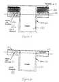
- FIG. 1begins with a partially completed BEOL interconnect structure that includes a conductive feature 122 formed in a low K dielectric 121 .
- the conductive feature 122can be any common conductor such as copper, tungsten, etc. and can serve the function of a wire, contact, stud, via, etc. depending upon the specific application and design and is referred to herein sometimes as a “metallic” or “copper” feature/conductor.
- FIG. 1also illustrates a chemical mechanical polishing (CMP) hard mask 125 and a reactive ion etching (RIE) mask 123 , 124 .
- CMPchemical mechanical polishing
- RIEreactive ion etching
- a chemical mechanical polishing processis applied to the structure shown in FIG. 1 to remove the uppermost portion of the metallic feature 122 and all of the RIE mask 123 , 124 .
- This polishing processcomprises (or is followed by) a short non-abrasive slurry polish that removes metallic residue and allows the surface 130 to be substantially uniform.
- This processingreduces the height of the structure to the level shown as 130 in FIG. 2 .
- This level 130is above the normal CMP polishing end point 126 (shown as dashed line in FIGS. 1 and 2 ).
- the structurewould be polished down to level 126 and then covered with a blanket high-K dielectric cap (which has the disadvantages that are discussed above).
- the inventionrecesses the metallic structure 122 (using a number of different processes discussed below) and then fills in the recessed portion with cap material (which may be an insulator or conductor).
- cap materialwhich may be an insulator or conductor.
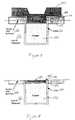
- FIG. 3One of the methods of recessing the metallic structures is shown in FIG. 3 .
- the upper portion of the metallic feature 122is oxidized to create an oxide portion 140 near the hard mask 125 .
- This oxidized portionis then removed using a wet or dry chemistry (RIE) that attacks oxides (as shown in FIG. 4 ). This results in the structure shown in FIG. 4 that includes a recess 150 above the metallic feature 122 .
- RIEwet or dry chemistry
- the depth of the recessis approximately equal to the height of the hard mask 125 .
- the hard maskcould be approximately 500 A thick and the recess could be approximately 500 A.
- the recesscan be made even deeper (e.g., >1000 A).
- the structure shown in FIG. 2can be subjected to an additional chemical etch or a dry etch that attacks the metallic feature 122 but does not substantially affect the hard mask 125 to create the recess 150 (thereby bypassing the processing shown in FIG. 3 ).
- the non-abrasive slurry polishing discussed abovecould be continued for additional time period such that a similar amount of the conductor 122 is removed to create the recess 150 and create the structure shown in FIG. 4 .
- a barrier layer 160is deposited over the structure and in the recess 150 .
- the layer 160is not formed and the processing proceeds directly from the structure shown in FIG. 4 to the structure shown in FIG. 7 (discussed in detail below) where the cap material 180 is deposited directly in the recess 150 .
- the barrier layer 160can be deposited on all surfaces (including vertical surfaces 165 ).
- the diffusion barrier 160can be deposited only on the horizontal surfaces (avoiding vertical surfaces 165 ), again depending upon the specific application. It is preferable to have the barrier layer 160 deposited in a conformal process that avoids the formation of voids within the recess 150 (e.g., electroless plating, directional physical vapor deposition, etc.).
- the layer 160comprises an electromigration inhibiting/diffusion barrier metal cap (e.g., CoWP, palladium, nickel, cobalt, antimony, chromium, molybdenum, platinum, ruthenium, rhodium, beryllium, hafnium, calcium, indium, cadmium, zinc, tin, tantalum and titanium) that prevents the conductor material 122 from diffusing into the cap material 180 (discussed below).
- an electromigration inhibiting/diffusion barrier metal cape.g., CoWP, palladium, nickel, cobalt, antimony, chromium, molybdenum, platinum, ruthenium, rhodium, beryllium, hafnium, calcium, indium, cadmium, zinc, tin, tantalum and titanium
- the barrier layer 160allows the cap to be made even thinner (since the barrier layer prevents metal diffusion from the metallic feature 122 into the cap 180 ). By reducing migration between the cap 180 and the conductor 122 , the barrier layer 160 enhances the electomigration lifetime (reduce migration of the conductor 122 ) which also reduces stress induced by such migration.
- the electromigration lifetime and stress induced voidingare dependent on atomic transport at the interface between the conductor 122 and the barrier layer 160 .
- the barrier layer 160reduces such atomic transport, thereby providing maximum reliability.
- the conductor migration rate(drift velocity) is a product of mobility (D/kT)*F; where D is the effective diffusivity of the conductor, T is the absolute temperature in Calvin, k is the Boltzman constant, and F is the driving force from the applied electrical field or stress gradient.
- the barrier 160also improves adhesion between the conductor 122 and the metal (or dielectric) 180 and acts as a corrosion protection layer.
- the barrier layer 160is conductive and would not be useful with conventional structures because it would cause shorting throughout the interconnect layer.
- the barrier layer 160is directly deposited within the recess and shown in FIG. 5 .
- a plasma vapor deposition (PVD) Pd seeding layer 170is deposited as shown in FIG. 6 .
- PVDplasma vapor deposition
- a pre-cleaning processe.g., acidic pre-clean, forming gas anneal, hydrogen plasma treatment, etc.
- the pre-cleaning and Pd seedingincreases the uniformity of the CoWP layer 160 .
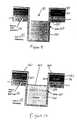
- FIG. 7illustrates the formation/deposition of the cap layer 180 .
- the cap layer 180can be formed directly in the recess 150 as shown in FIG.
- various barrier layers 160 , 170can optionally be included before the cap layer 180 is deposited, as shown in FIG. 6 . It is preferable to have the cap layer 180 deposited in a conformal process that avoids the formation of voids within the recess 150 . It is also preferable to have the cap layer 180 deposited following the deposition of barrier layer 160 , 170 without exposing the substrate to the air.
- the cap layercan be a conductor or an insulator.
- the cap layercan comprise insulating materials including SiO 2 , Boron-doped SiO 2 , BPSG (Boron Phosphorous Silicate Glass), Silicon Carbide, Nitrogen doped silicon carbide, oxides, Si 3 N 4 , etc., and generally has a substantially higher dielectric constant than the low-K dielectric 121 or metallic materials such as TaN, TiN, TiSiN, Ta, W, etc. and generally has a good adhesion with low K dielectric material and also a good Copper and Oxygen barrier. As shown in FIG.
- a chemical mechanical polishing processplanarizes the structure down to level 126 , thereby leaving caps 180 (and any optional layers 160 , 170 ) only within the recess 150 above the conductor 122 and creating multiple caps along the upper surface of the interconnection layer. Therefore, with the inventive process, the cap material 180 does not comprise a blanket layer but, instead the cap material 180 comprising distinct and separate caps positioned only above the conductors 122 throughout the interconnect layer. As mentioned above, this substantially reduces the volume of cap material included within the BEOL interconnection layer.
- FIGS. 9-12illustrate yet another embodiment of the invention that forms the recess 151 while leaving the RIE mask 123 , 124 intact. Therefore, this embodiment is different than the embodiment shown in FIG. 2 because the RIE mask 123 , 124 shown in FIG. 1 is not removed before the recess 151 is formed (as shown and FIG. 9 ).
- the processes for forming the recess 151are the same as those discussed above and are simply performed without the step shown in FIG. 2 of removing the RIE mask 123 , 124 .
- FIG. 10illustrates the formation of the barrier layer 160 .
- this embodimentillustrates that the barrier layer does not need to be formed on the sidewalls 165 of the recess 151 .
- the barrier layer 160can be formed on all surfaces or only on the horizontal surfaces.
- this embodimentdoes not utilize the optional Pd seeding layer 170 (however, it could).
- the cap material 180is deposited (as discussed above) and in FIG. 12 the structure is planarized to result in a substantially similar structure to that shown in FIG. 8 .
- the use of a blanket dielectric capalters the dielectric constant of the BEOL interconnection layer undesirably, because the cap must be a certain thickness to be an effective barrier.
- this thicknessusually does not scale as line width and thickness are reduced (from processing generation to processing generation).
- the inventionuses a selective cap process (described above) to leave the cap material only on the metal features (and not between metal features). This process and structure greatly reduce the amount of higher-K dielectric cap material used in the BEOL interconnect layer.
- some embodiments of the inventioninclude a barrier layer 160 between the metallic feature 122 and the cap 180 .
- the barrier layer 160enhances the electromigration lifetime (reduce migration of the conductor 122 ) which also reduces stress induced by such migration.
- the barrier 160also improves adhesion between the conductor 122 and the metal or dielectric cap 180 and acts as a corrosion protection layer.
- the barrier layer 160is conductive and would not be useful with conventional blanket type structures because a blanket layer of a conductor would cause shorting throughout the interconnect layer.
- the inventive structureis also useful with imbedded etch stopping layers because the cap material does not disrupt the effectiveness of the etch stopping layer, as a conventional blanket dielectric cap would.
Landscapes
- Engineering & Computer Science (AREA)
- Physics & Mathematics (AREA)
- Condensed Matter Physics & Semiconductors (AREA)
- General Physics & Mathematics (AREA)
- Computer Hardware Design (AREA)
- Microelectronics & Electronic Packaging (AREA)
- Power Engineering (AREA)
- Manufacturing & Machinery (AREA)
- Internal Circuitry In Semiconductor Integrated Circuit Devices (AREA)
Abstract
Description
- 1. Field of the Invention
- The present invention generally relates to insulators/conductors above copper wiring connections on exterior interconnection layers of an integrated circuit structure, and more particularly to an improved process and structure for forming such interconnection layers.
- 2. Description of the Related Art
- Integrated circuit processing can be generally divided into front end of line (FEOL) and back and of line (BEOL) processes. During FEOL processing, the various logical and functional devices are manufactured. The FEOL processing will generally form many layers of logical and functional devices. Layers of interconnections are formed above these logical and functional layers during the BEOL processing to complete the integrated circuit structure. Therefore, BEOL processing generally involves the formation of insulators and conductive wiring and contacts.
- Recently, insulators (dielectrics) that have a lower dielectric constant (and are softer) are replacing older, harder, higher dielectric constant insulators. Lower dielectric constant materials generally have a dielectric constant below 3.0 and include polymeric low K dielectrics commercial products such as SiLK, available from Dow Chemical Company, NY, USA, FLARE, available from Honeywell, NJ, USA, microporous glasses such as Nanoglass (Porous SiO2), available from Honeywell, Inc., NJ, USA, as well as Black Diamond (Carbon-doped SiO2), available from Applied Material, CA, USA; Coral (Silicon carbide based dielectrics), available from Novellus Systems, Inc., CA, USA; and Xerogel, available from Allied Signal, NJ, USA. These lower dielectric constant insulators are referred to as “low-K” dielectrics. These low-K dielectrics are advantageous because they decrease overall capacitance, which increases device speed and allows lower voltages to be utilized (making the device smaller and less expensive).
- Metals (such as copper, tungsten, etc.) are generally used as wiring and electrical connections in the BEOL interconnection layers. One drawback of using low-K dielectrics in the BEOL interconnection layers is that the low-K dielectrics are more sensitive to metal migration (e.g., copper migration) than were the higher-K dielectrics. One conventional solution to this problem is to use a blanket dielectric cap (having a high dielectric constant) as a metal diffusion barrier for low K dielectric material above the metal features. This blanket dielectric cap also acts as an oxygen barrier to prevent oxygen in the low k dielectric material from oxidizing the metal.
- However, this dielectric cap usually has higher dielectric constant and will greatly affect the effective dielectric constant of the overall dielectric material between metal features. In addition, the dielectric cap generally needs to have a minimum thickness (e.g., 250 A) to be effective. However, if the dielectric cap is formed above a certain thickness, it will substantially distort the dielectric constant of the interconnect layer above a desired level. Therefore, there is a need for a new type of interconnection layer that does not require a blanket dielectric cap. The invention described below provides a method and structure for creating such an interconnection layer.
- The invention provides an integrated circuit structure that has at least one layer of logical and functional devices and at least one interconnection layer above the layer of logical and functional devices. The interconnection layer has a substrate, conductive features within the substrate, and caps positioned only above the conductive features.
- The invention can also have a barrier layer between the conductive features and the caps. The barrier layer can be a conductive material. The interconnection layer has an upper surface and the caps are positioned along the upper surface. The invention has a mask material along the upper surface and adjacent to the conductive features. The substrate has a lower dielectric constant than the mask which is below 3.0.
- The invention also provides a method for selectively capping metal features of an interconnect structure. The interconnect structure is positioned above at least one layer of logical and functional devices. The invention recesses the metal features and then deposits a cap layer over the interconnect structure. The invention then planarizes the interconnect structure to form caps only above the metal features.
- The invention will be better understood from the following detailed description of preferred embodiments of the invention with reference to the drawings, in which:
FIG. 1 is a schematic diagram of a partially completed integrated circuit structure according to the invention;FIG. 2 is a schematic diagram of a partially completed integrated circuit structure according to the invention;FIG. 3 is a schematic diagram of a partially completed integrated circuit structure according to the invention;FIG. 4 is a schematic diagram of a partially completed integrated circuit structure according to the invention;FIG. 5 is a schematic diagram of a partially completed integrated circuit structure according to the invention;FIG. 6 is a schematic diagram of a partially completed integrated circuit structure according to the invention;FIG. 7 is a schematic diagram of a partially completed integrated circuit structure according to the invention;FIG. 8 is a schematic diagram of a partially completed integrated circuit structure according to the invention;FIG. 9 is a schematic diagram of a partially completed integrated circuit structure according to the invention;FIG. 10 is a schematic diagram of a partially completed integrated circuit structure according to the invention;FIG. 11 is a schematic diagram of a partially completed integrated circuit structure according to the invention; andFIG. 12 is a schematic diagram of a partially completed integrated circuit structure according to the invention.- As mentioned above, the conventional use of a high-K dielectric cap presents a number of disadvantages. The invention overcomes such disadvantages by forming the cap material only above metal areas such as wiring and interlevel interconnections. More specifically, as shown below, the invention polishes the interconnection layer down to a predetermined level, forms recesses in the tops of the metal portions, deposits the cap material over the entire interconnection layer, and then polishes the interconnection layer so that the cap material only remains within the recesses above the metal portions. Performing such processing, the invention substantially reduces the amount of high-K dielectric cap material within the structure, thereby avoiding the problems that are encountered when a blanket layer of dielectric cap material is utilized (discussed above).
- The processing used to achieve the inventive structure is shown in
FIGS. 1-12 , which represent multiple embodiments of the present invention.FIG. 1 begins with a partially completed BEOL interconnect structure that includes aconductive feature 122 formed in a low K dielectric121. Theconductive feature 122 can be any common conductor such as copper, tungsten, etc. and can serve the function of a wire, contact, stud, via, etc. depending upon the specific application and design and is referred to herein sometimes as a “metallic” or “copper” feature/conductor. - A
liner 120 is in place around themetallic feature 122 to prevent themetallic feature 122 from diffusing into thelow k dielectrics 121.FIG. 1 also illustrates a chemical mechanical polishing (CMP)hard mask 125 and a reactive ion etching (RIE)mask FIG. 1 are well-known and are not discussed herein for brevity, and so as to not obscure the salient features of the invention. - A chemical mechanical polishing process is applied to the structure shown in
FIG. 1 to remove the uppermost portion of themetallic feature 122 and all of theRIE mask surface 130 to be substantially uniform. This processing reduces the height of the structure to the level shown as130 inFIG. 2 . Thislevel 130 is above the normal CMP polishing end point126 (shown as dashed line inFIGS. 1 and 2 ). Conventionally, the structure would be polished down tolevel 126 and then covered with a blanket high-K dielectric cap (which has the disadvantages that are discussed above). - Rather than forming a blanket high-K dielectric cap as is done conventionally, the invention recesses the metallic structure122 (using a number of different processes discussed below) and then fills in the recessed portion with cap material (which may be an insulator or conductor). One of the methods of recessing the metallic structures is shown in
FIG. 3 . In this process, the upper portion of themetallic feature 122 is oxidized to create an oxide portion140 near thehard mask 125. This oxidized portion is then removed using a wet or dry chemistry (RIE) that attacks oxides (as shown inFIG. 4 ). This results in the structure shown inFIG. 4 that includes arecess 150 above themetallic feature 122. The depth of the recess is approximately equal to the height of thehard mask 125. For example, the hard mask could be approximately 500 A thick and the recess could be approximately 500 A. Depending upon the application and the desired overall dielectric constant, the recess can be made even deeper (e.g., >1000 A). - Alternatively, rather than creating the oxide140, the structure shown in
FIG. 2 can be subjected to an additional chemical etch or a dry etch that attacks themetallic feature 122 but does not substantially affect thehard mask 125 to create the recess150 (thereby bypassing the processing shown inFIG. 3 ). For example, the non-abrasive slurry polishing discussed above could be continued for additional time period such that a similar amount of theconductor 122 is removed to create therecess 150 and create the structure shown inFIG. 4 . - In any case, once the structure shown in
FIG. 4 is created, in some embodiments of the invention, abarrier layer 160 is deposited over the structure and in therecess 150. In some other embodiments, thelayer 160 is not formed and the processing proceeds directly from the structure shown inFIG. 4 to the structure shown inFIG. 7 (discussed in detail below) where thecap material 180 is deposited directly in therecess 150. Thebarrier layer 160 can be deposited on all surfaces (including vertical surfaces165). Alternatively, thediffusion barrier 160 can be deposited only on the horizontal surfaces (avoiding vertical surfaces165), again depending upon the specific application. It is preferable to have thebarrier layer 160 deposited in a conformal process that avoids the formation of voids within the recess150 (e.g., electroless plating, directional physical vapor deposition, etc.). - The chemical makeup of the
barrier material 160 that will be utilized is different depending upon each specific design. For example, in one embodiment, thelayer 160 comprises an electromigration inhibiting/diffusion barrier metal cap (e.g., CoWP, palladium, nickel, cobalt, antimony, chromium, molybdenum, platinum, ruthenium, rhodium, beryllium, hafnium, calcium, indium, cadmium, zinc, tin, tantalum and titanium) that prevents theconductor material 122 from diffusing into the cap material180 (discussed below). - The
barrier layer 160 allows the cap to be made even thinner (since the barrier layer prevents metal diffusion from themetallic feature 122 into the cap180). By reducing migration between thecap 180 and theconductor 122, thebarrier layer 160 enhances the electomigration lifetime (reduce migration of the conductor122) which also reduces stress induced by such migration. - The electromigration lifetime and stress induced voiding are dependent on atomic transport at the interface between the
conductor 122 and thebarrier layer 160. Thebarrier layer 160 reduces such atomic transport, thereby providing maximum reliability. The conductor migration rate (drift velocity) is a product of mobility (D/kT)*F; where D is the effective diffusivity of the conductor, T is the absolute temperature in Calvin, k is the Boltzman constant, and F is the driving force from the applied electrical field or stress gradient. - The
barrier 160 also improves adhesion between theconductor 122 and the metal (or dielectric)180 and acts as a corrosion protection layer. Thebarrier layer 160 is conductive and would not be useful with conventional structures because it would cause shorting throughout the interconnect layer. - In one embodiment the
barrier layer 160 is directly deposited within the recess and shown inFIG. 5 . In another embodiment, before thebarrier layer 160 is formed, a plasma vapor deposition (PVD)Pd seeding layer 170 is deposited as shown inFIG. 6 . A pre-cleaning process (e.g., acidic pre-clean, forming gas anneal, hydrogen plasma treatment, etc.) may proceed thePd seeding layer 170 deposition. The pre-cleaning and Pd seeding increases the uniformity of theCoWP layer 160.FIG. 7 illustrates the formation/deposition of thecap layer 180. As mentioned previously, thecap layer 180 can be formed directly in therecess 150 as shown inFIG. 5 or,various barrier layers cap layer 180 is deposited, as shown inFIG. 6 . It is preferable to have thecap layer 180 deposited in a conformal process that avoids the formation of voids within therecess 150. It is also preferable to have thecap layer 180 deposited following the deposition ofbarrier layer - The cap layer can be a conductor or an insulator. The cap layer can comprise insulating materials including SiO2, Boron-doped SiO2, BPSG (Boron Phosphorous Silicate Glass), Silicon Carbide, Nitrogen doped silicon carbide, oxides, Si3N4, etc., and generally has a substantially higher dielectric constant than the low-
K dielectric 121 or metallic materials such as TaN, TiN, TiSiN, Ta, W, etc. and generally has a good adhesion with low K dielectric material and also a good Copper and Oxygen barrier. As shown inFIG. 8 , a chemical mechanical polishing process planarizes the structure down tolevel 126, thereby leaving caps180 (and anyoptional layers 160,170) only within therecess 150 above theconductor 122 and creating multiple caps along the upper surface of the interconnection layer. Therefore, with the inventive process, thecap material 180 does not comprise a blanket layer but, instead thecap material 180 comprising distinct and separate caps positioned only above theconductors 122 throughout the interconnect layer. As mentioned above, this substantially reduces the volume of cap material included within the BEOL interconnection layer. FIGS. 9-12 illustrate yet another embodiment of the invention that forms therecess 151 while leaving theRIE mask FIG. 2 because theRIE mask FIG. 1 is not removed before therecess 151 is formed (as shown andFIG. 9 ). The processes for forming therecess 151 are the same as those discussed above and are simply performed without the step shown inFIG. 2 of removing theRIE mask FIG. 10 illustrates the formation of thebarrier layer 160. However, this embodiment illustrates that the barrier layer does not need to be formed on thesidewalls 165 of therecess 151. As with the previous embodiments, thebarrier layer 160 can be formed on all surfaces or only on the horizontal surfaces. In addition, this embodiment does not utilize the optional Pd seeding layer170 (however, it could). InFIG. 11 , thecap material 180 is deposited (as discussed above) and inFIG. 12 the structure is planarized to result in a substantially similar structure to that shown inFIG. 8 .- As shown above, the use of a blanket dielectric cap alters the dielectric constant of the BEOL interconnection layer undesirably, because the cap must be a certain thickness to be an effective barrier. However, this thickness usually does not scale as line width and thickness are reduced (from processing generation to processing generation). The invention uses a selective cap process (described above) to leave the cap material only on the metal features (and not between metal features). This process and structure greatly reduce the amount of higher-K dielectric cap material used in the BEOL interconnect layer.
- In addition, some embodiments of the invention include a
barrier layer 160 between themetallic feature 122 and thecap 180. By reducing surface diffusion of theconductor 122, thebarrier layer 160 enhances the electromigration lifetime (reduce migration of the conductor122) which also reduces stress induced by such migration. Thebarrier 160 also improves adhesion between theconductor 122 and the metal ordielectric cap 180 and acts as a corrosion protection layer. Thebarrier layer 160 is conductive and would not be useful with conventional blanket type structures because a blanket layer of a conductor would cause shorting throughout the interconnect layer. The inventive structure is also useful with imbedded etch stopping layers because the cap material does not disrupt the effectiveness of the etch stopping layer, as a conventional blanket dielectric cap would. - While the invention has been described in terms of preferred embodiments, those skilled in the art will recognize that the invention can be practiced with modification within the spirit and scope of the appended claims.
Claims (13)
1-19. (canceled)
20. A method for selectively capping metal features of an interconnect structure, wherein said interconnect structure is positioned above at least one layer of logical and functional devices, said method comprising:
recessing said metal features;
depositing a cap layer over said interconnect structure; and
planarizing said interconnect structure to form caps only above said metal features.
21. The method inclaim 20 , further comprising, before said depositing of said cap layer, depositing a barrier layer above recessed metal features produced by said recessing process.
22. The method inclaim 20 , wherein said depositing of said barrier layer comprises electroless plating.
23. The method inclaim 20 , wherein said cap layer comprises one of a metal material and a dielectric material.
24. The method inclaim 20 , wherein said interconnection structure includes an upper surface and said depositing and planarizing processes form said caps along said upper surface.
25. The method inclaim 20 , wherein said planarizing process stops on mask material positioned adjacent to said conductive features and along an upper surface of said interconnection structure.
26. A method of forming an integrated circuit structure, said method comprising:
forming at least one layer of logical and functional devices;
forming at least one interconnection layer above said layer of logical and functional devices,
wherein said forming of said interconnection layer comprises:
forming an insulator layer;
forming metal features in said insulator layer;
recessing said metal features;
depositing a cap layer over said insulator layer; and
planarizing said insulator layer to form caps only above said metal features.
27. The method inclaim 26 , further comprising, before said depositing of said cap layer, depositing a barrier layer above recessed metal features produced by said recessing process.
28. The method inclaim 26 , wherein said depositing of said barrier layer comprises electroless plating.
29. The method inclaim 26 , wherein said cap layer comprises one of a metal material and a dielectric material.
30. The method inclaim 26 , wherein said insulator layer includes an upper surface and said depositing and planarizing processes form said caps along said upper surface.
31. The method inclaim 26 , wherein said planarizing process stops on mask material positioned adjacent to said conductive features and along an upper surface of said insulator layer.
Priority Applications (1)
| Application Number | Priority Date | Filing Date | Title |
|---|---|---|---|
| US11/058,783US7064064B2 (en) | 2002-12-16 | 2005-02-16 | Copper recess process with application to selective capping and electroless plating |
Applications Claiming Priority (2)
| Application Number | Priority Date | Filing Date | Title |
|---|---|---|---|
| US10/319,967US6975032B2 (en) | 2002-12-16 | 2002-12-16 | Copper recess process with application to selective capping and electroless plating |
| US11/058,783US7064064B2 (en) | 2002-12-16 | 2005-02-16 | Copper recess process with application to selective capping and electroless plating |
Related Parent Applications (1)
| Application Number | Title | Priority Date | Filing Date |
|---|---|---|---|
| US10/319,967DivisionUS6975032B2 (en) | 2002-12-16 | 2002-12-16 | Copper recess process with application to selective capping and electroless plating |
Publications (2)
| Publication Number | Publication Date |
|---|---|
| US20050158985A1true US20050158985A1 (en) | 2005-07-21 |
| US7064064B2 US7064064B2 (en) | 2006-06-20 |
Family
ID=32506759
Family Applications (2)
| Application Number | Title | Priority Date | Filing Date |
|---|---|---|---|
| US10/319,967Expired - LifetimeUS6975032B2 (en) | 2002-12-16 | 2002-12-16 | Copper recess process with application to selective capping and electroless plating |
| US11/058,783Expired - LifetimeUS7064064B2 (en) | 2002-12-16 | 2005-02-16 | Copper recess process with application to selective capping and electroless plating |
Family Applications Before (1)
| Application Number | Title | Priority Date | Filing Date |
|---|---|---|---|
| US10/319,967Expired - LifetimeUS6975032B2 (en) | 2002-12-16 | 2002-12-16 | Copper recess process with application to selective capping and electroless plating |
Country Status (4)
| Country | Link |
|---|---|
| US (2) | US6975032B2 (en) |
| JP (1) | JP2004200684A (en) |
| CN (1) | CN100428430C (en) |
| TW (1) | TWI241701B (en) |
Cited By (13)
| Publication number | Priority date | Publication date | Assignee | Title |
|---|---|---|---|---|
| US20040113277A1 (en)* | 2002-12-11 | 2004-06-17 | Chiras Stefanie Ruth | Formation of aligned capped metal lines and interconnections in multilevel semiconductor structures |
| US20070105377A1 (en)* | 2003-10-20 | 2007-05-10 | Novellus Systems, Inc. | Fabrication of semiconductor interconnect structure |
| US7338908B1 (en) | 2003-10-20 | 2008-03-04 | Novellus Systems, Inc. | Method for fabrication of semiconductor interconnect structure with reduced capacitance, leakage current, and improved breakdown voltage |
| US20090032964A1 (en)* | 2007-07-31 | 2009-02-05 | Micron Technology, Inc. | System and method for providing semiconductor device features using a protective layer |
| US7605082B1 (en) | 2005-10-13 | 2009-10-20 | Novellus Systems, Inc. | Capping before barrier-removal IC fabrication method |
| US20100015805A1 (en)* | 2003-10-20 | 2010-01-21 | Novellus Systems, Inc. | Wet Etching Methods for Copper Removal and Planarization in Semiconductor Processing |
| US20100029088A1 (en)* | 2003-10-20 | 2010-02-04 | Novellus Systems, Inc. | Modulated metal removal using localized wet etching |
| US20110056913A1 (en)* | 2009-09-02 | 2011-03-10 | Mayer Steven T | Reduced isotropic etchant material consumption and waste generation |
| US7972970B2 (en) | 2003-10-20 | 2011-07-05 | Novellus Systems, Inc. | Fabrication of semiconductor interconnect structure |
| US20120313250A1 (en)* | 2011-06-08 | 2012-12-13 | International Business Machines Corporation | Forming Features on a Substrate Having Varying Feature Densities |
| US8470191B2 (en) | 2003-10-20 | 2013-06-25 | Novellus Systems, Inc. | Topography reduction and control by selective accelerator removal |
| CN105720004A (en)* | 2014-12-04 | 2016-06-29 | 中芯国际集成电路制造(上海)有限公司 | Formation method of semiconductor structure |
| KR20210004231A (en)* | 2019-07-03 | 2021-01-13 | 삼성전자주식회사 | Integrated circuit device and method of manufacturing the same |
Families Citing this family (115)
| Publication number | Priority date | Publication date | Assignee | Title |
|---|---|---|---|---|
| US7262133B2 (en)* | 2003-01-07 | 2007-08-28 | Applied Materials, Inc. | Enhancement of copper line reliability using thin ALD tan film to cap the copper line |
| US7420275B1 (en) | 2003-09-24 | 2008-09-02 | Novellus Systems, Inc. | Boron-doped SIC copper diffusion barrier films |
| US6967405B1 (en)* | 2003-09-24 | 2005-11-22 | Yongsik Yu | Film for copper diffusion barrier |
| US20050110142A1 (en)* | 2003-11-26 | 2005-05-26 | Lane Michael W. | Diffusion barriers formed by low temperature deposition |
| US7282438B1 (en) | 2004-06-15 | 2007-10-16 | Novellus Systems, Inc. | Low-k SiC copper diffusion barrier films |
| US8882914B2 (en)* | 2004-09-17 | 2014-11-11 | Intermolecular, Inc. | Processing substrates using site-isolated processing |
| US20060292846A1 (en)* | 2004-09-17 | 2006-12-28 | Pinto Gustavo A | Material management in substrate processing |
| US7390739B2 (en)* | 2005-05-18 | 2008-06-24 | Lazovsky David E | Formation of a masking layer on a dielectric region to facilitate formation of a capping layer on electrically conductive regions separated by the dielectric region |
| US20060060301A1 (en)* | 2004-09-17 | 2006-03-23 | Lazovsky David E | Substrate processing using molecular self-assembly |
| US7749881B2 (en)* | 2005-05-18 | 2010-07-06 | Intermolecular, Inc. | Formation of a masking layer on a dielectric region to facilitate formation of a capping layer on electrically conductive regions separated by the dielectric region |
| US8084400B2 (en)* | 2005-10-11 | 2011-12-27 | Intermolecular, Inc. | Methods for discretized processing and process sequence integration of regions of a substrate |
| KR100597646B1 (en)* | 2004-10-01 | 2006-07-05 | 삼성전자주식회사 | Floating gate manufacturing method of flash memory |
| US7879710B2 (en)* | 2005-05-18 | 2011-02-01 | Intermolecular, Inc. | Substrate processing including a masking layer |
| US7309658B2 (en)* | 2004-11-22 | 2007-12-18 | Intermolecular, Inc. | Molecular self-assembly in substrate processing |
| DE102005004384A1 (en)* | 2005-01-31 | 2006-08-10 | Advanced Micro Devices, Inc., Sunnyvale | A method of making a defined recess in a damascene structure using a CMP process and a damascene structure |
| US7265048B2 (en)* | 2005-03-01 | 2007-09-04 | Applied Materials, Inc. | Reduction of copper dewetting by transition metal deposition |
| US7335588B2 (en)* | 2005-04-15 | 2008-02-26 | International Business Machines Corporation | Interconnect structure and method of fabrication of same |
| US7317253B2 (en) | 2005-04-25 | 2008-01-08 | Sony Corporation | Cobalt tungsten phosphate used to fill voids arising in a copper metallization process |
| JP5382988B2 (en)* | 2005-09-28 | 2014-01-08 | 三星電子株式会社 | Method for forming a metal wiring structure |
| US8776717B2 (en)* | 2005-10-11 | 2014-07-15 | Intermolecular, Inc. | Systems for discretized processing of regions of a substrate |
| US7955436B2 (en)* | 2006-02-24 | 2011-06-07 | Intermolecular, Inc. | Systems and methods for sealing in site-isolated reactors |
| US7544574B2 (en)* | 2005-10-11 | 2009-06-09 | Intermolecular, Inc. | Methods for discretized processing of regions of a substrate |
| KR100729126B1 (en)* | 2005-11-15 | 2007-06-14 | 동부일렉트로닉스 주식회사 | Metal wiring of semiconductor device and method of forming the same |
| EP1994550A4 (en)* | 2006-02-10 | 2012-01-11 | Intermolecular Inc | Method and apparatus for combinatorially varying materials, unit process and process sequence |
| US8772772B2 (en)* | 2006-05-18 | 2014-07-08 | Intermolecular, Inc. | System and method for increasing productivity of combinatorial screening |
| US8367543B2 (en)* | 2006-03-21 | 2013-02-05 | International Business Machines Corporation | Structure and method to improve current-carrying capabilities of C4 joints |
| US8193087B2 (en) | 2006-05-18 | 2012-06-05 | Taiwan Semiconductor Manufacturing Co., Ltd. | Process for improving copper line cap formation |
| KR100752195B1 (en)* | 2006-09-08 | 2007-08-27 | 동부일렉트로닉스 주식회사 | Wiring Formation Method of Semiconductor Device |
| TWI315560B (en)* | 2006-09-19 | 2009-10-01 | Nat Univ Tsing Hua | Interconnection structure and manufacturing method thereof |
| US7569475B2 (en)* | 2006-11-15 | 2009-08-04 | International Business Machines Corporation | Interconnect structure having enhanced electromigration reliability and a method of fabricating same |
| US20080157382A1 (en)* | 2006-12-28 | 2008-07-03 | Chinthakindi Anil K | Direct termination of a wiring metal in a semiconductor device |
| US8011317B2 (en)* | 2006-12-29 | 2011-09-06 | Intermolecular, Inc. | Advanced mixing system for integrated tool having site-isolated reactors |
| US7915166B1 (en) | 2007-02-22 | 2011-03-29 | Novellus Systems, Inc. | Diffusion barrier and etch stop films |
| US7859113B2 (en)* | 2007-02-27 | 2010-12-28 | International Business Machines Corporation | Structure including via having refractory metal collar at copper wire and dielectric layer liner-less interface and related method |
| US8173537B1 (en) | 2007-03-29 | 2012-05-08 | Novellus Systems, Inc. | Methods for reducing UV and dielectric diffusion barrier interaction |
| US20080236619A1 (en)* | 2007-04-02 | 2008-10-02 | Enthone Inc. | Cobalt capping surface preparation in microelectronics manufacture |
| US7790599B2 (en)* | 2007-04-13 | 2010-09-07 | International Business Machines Corporation | Metal cap for interconnect structures |
| US7732924B2 (en) | 2007-06-12 | 2010-06-08 | International Business Machines Corporation | Semiconductor wiring structures including dielectric cap within metal cap layer |
| US8138604B2 (en)* | 2007-06-21 | 2012-03-20 | International Business Machines Corporation | Metal cap with ultra-low k dielectric material for circuit interconnect applications |
| US7884018B2 (en)* | 2007-06-21 | 2011-02-08 | International Business Machines Corporation | Method for improving the selectivity of a CVD process |
| US7737028B2 (en)* | 2007-09-28 | 2010-06-15 | Applied Materials, Inc. | Selective ruthenium deposition on copper materials |
| US20090133908A1 (en)* | 2007-11-28 | 2009-05-28 | Goodner Michael D | Interconnect structure for a microelectronic device, method of manfacturing same, and microelectronic structure containing same |
| US7998864B2 (en)* | 2008-01-29 | 2011-08-16 | International Business Machines Corporation | Noble metal cap for interconnect structures |
| US20090200668A1 (en)* | 2008-02-07 | 2009-08-13 | International Business Machines Corporation | Interconnect structure with high leakage resistance |
| US7834457B2 (en)* | 2008-02-28 | 2010-11-16 | International Business Machines Corporation | Bilayer metal capping layer for interconnect applications |
| US7830010B2 (en) | 2008-04-03 | 2010-11-09 | International Business Machines Corporation | Surface treatment for selective metal cap applications |
| US8124522B1 (en) | 2008-04-11 | 2012-02-28 | Novellus Systems, Inc. | Reducing UV and dielectric diffusion barrier interaction through the modulation of optical properties |
| US7687877B2 (en)* | 2008-05-06 | 2010-03-30 | International Business Machines Corporation | Interconnect structure with a mushroom-shaped oxide capping layer and method for fabricating same |
| US7956466B2 (en) | 2008-05-09 | 2011-06-07 | International Business Machines Corporation | Structure for interconnect structure containing various capping materials for electrical fuse and other related applications |
| US8772156B2 (en)* | 2008-05-09 | 2014-07-08 | International Business Machines Corporation | Methods of fabricating interconnect structures containing various capping materials for electrical fuse and other related applications |
| DE102008026211B4 (en)* | 2008-05-30 | 2010-07-08 | Advanced Micro Devices, Inc., Sunnyvale | A method of fabricating a semiconductor device having metal lines with a selectively formed dielectric capping layer |
| US8354751B2 (en)* | 2008-06-16 | 2013-01-15 | International Business Machines Corporation | Interconnect structure for electromigration enhancement |
| US8013446B2 (en)* | 2008-08-12 | 2011-09-06 | International Business Machines Corporation | Nitrogen-containing metal cap for interconnect structures |
| US8232645B2 (en) | 2008-08-14 | 2012-07-31 | International Business Machines Corporation | Interconnect structures, design structure and method of manufacture |
| DE102008044964B4 (en)* | 2008-08-29 | 2015-12-17 | Globalfoundries Dresden Module One Limited Liability Company & Co. Kg | Reduction of leakage currents and dielectric breakdown in dielectric materials of metallization systems of semiconductor devices through the production of recesses |
| US8823176B2 (en)* | 2008-10-08 | 2014-09-02 | International Business Machines Corporation | Discontinuous/non-uniform metal cap structure and process for interconnect integration |
| US8232625B2 (en)* | 2009-03-26 | 2012-07-31 | International Business Machines Corporation | ESD network circuit with a through wafer via structure and a method of manufacture |
| US7928570B2 (en)* | 2009-04-16 | 2011-04-19 | International Business Machines Corporation | Interconnect structure |
| US8054597B2 (en)* | 2009-06-23 | 2011-11-08 | International Business Machines Corporation | Electrostatic discharge structures and methods of manufacture |
| US8039966B2 (en)* | 2009-09-03 | 2011-10-18 | International Business Machines Corporation | Structures of and methods and tools for forming in-situ metallic/dielectric caps for interconnects |
| US8617986B2 (en) | 2009-11-09 | 2013-12-31 | Taiwan Semiconductor Manufacturing Company, Ltd. | Integrated circuits and methods for forming the integrated circuits |
| US8247332B2 (en)* | 2009-12-04 | 2012-08-21 | Novellus Systems, Inc. | Hardmask materials |
| US8299365B2 (en)* | 2010-01-07 | 2012-10-30 | International Business Machines Corporation | Self-aligned composite M-MOx/dielectric cap for Cu interconnect structures |
| US8404582B2 (en)* | 2010-05-04 | 2013-03-26 | International Business Machines Corporation | Structure and method for manufacturing interconnect structures having self-aligned dielectric caps |
| US8809183B2 (en) | 2010-09-21 | 2014-08-19 | International Business Machines Corporation | Interconnect structure with a planar interface between a selective conductive cap and a dielectric cap layer |
| US8912658B2 (en)* | 2010-10-29 | 2014-12-16 | International Business Machines Corporation | Interconnect structure with enhanced reliability |
| US8664113B2 (en) | 2011-04-28 | 2014-03-04 | GlobalFoundries, Inc. | Multilayer interconnect structure and method for integrated circuits |
| US8877645B2 (en) | 2011-09-15 | 2014-11-04 | International Business Machines Corporation | Integrated circuit structure having selectively formed metal cap |
| JP5764445B2 (en) | 2011-09-21 | 2015-08-19 | 東京エレクトロン株式会社 | Manufacturing method of semiconductor device |
| US8492274B2 (en) | 2011-11-07 | 2013-07-23 | International Business Machines Corporation | Metal alloy cap integration |
| US8796853B2 (en)* | 2012-02-24 | 2014-08-05 | International Business Machines Corporation | Metallic capped interconnect structure with high electromigration resistance and low resistivity |
| US9034664B2 (en)* | 2012-05-16 | 2015-05-19 | International Business Machines Corporation | Method to resolve hollow metal defects in interconnects |
| US10211310B2 (en) | 2012-06-12 | 2019-02-19 | Novellus Systems, Inc. | Remote plasma based deposition of SiOC class of films |
| US10832904B2 (en) | 2012-06-12 | 2020-11-10 | Lam Research Corporation | Remote plasma based deposition of oxygen doped silicon carbide films |
| US10325773B2 (en) | 2012-06-12 | 2019-06-18 | Novellus Systems, Inc. | Conformal deposition of silicon carbide films |
| US9234276B2 (en) | 2013-05-31 | 2016-01-12 | Novellus Systems, Inc. | Method to obtain SiC class of films of desired composition and film properties |
| US9659869B2 (en)* | 2012-09-28 | 2017-05-23 | Intel Corporation | Forming barrier walls, capping, or alloys /compounds within metal lines |
| US9337068B2 (en) | 2012-12-18 | 2016-05-10 | Lam Research Corporation | Oxygen-containing ceramic hard masks and associated wet-cleans |
| US9312203B2 (en) | 2013-01-02 | 2016-04-12 | Globalfoundries Inc. | Dual damascene structure with liner |
| CN103928389B (en)* | 2013-01-10 | 2017-02-22 | 中芯国际集成电路制造(上海)有限公司 | Forming method of semiconductor structure |
| CN104112701B (en)* | 2013-04-18 | 2017-05-03 | 中芯国际集成电路制造(上海)有限公司 | Semiconductor structure and manufacturing method thereof |
| US9171801B2 (en) | 2013-05-09 | 2015-10-27 | Globalfoundries U.S. 2 Llc | E-fuse with hybrid metallization |
| US9536830B2 (en) | 2013-05-09 | 2017-01-03 | Globalfoundries Inc. | High performance refractory metal / copper interconnects to eliminate electromigration |
| US9305879B2 (en) | 2013-05-09 | 2016-04-05 | Globalfoundries Inc. | E-fuse with hybrid metallization |
| US8962479B2 (en) | 2013-05-10 | 2015-02-24 | International Business Machines Corporation | Interconnect structures containing nitrided metallic residues |
| US10297442B2 (en) | 2013-05-31 | 2019-05-21 | Lam Research Corporation | Remote plasma based deposition of graded or multi-layered silicon carbide film |
| US9558999B2 (en) | 2013-09-12 | 2017-01-31 | Globalfoundries Inc. | Ultra-thin metal wires formed through selective deposition |
| US9318414B2 (en) | 2013-10-29 | 2016-04-19 | Globalfoundries Inc. | Integrated circuit structure with through-semiconductor via |
| US9318413B2 (en)* | 2013-10-29 | 2016-04-19 | Globalfoundries Inc. | Integrated circuit structure with metal cap and methods of fabrication |
| US9202749B2 (en) | 2014-02-06 | 2015-12-01 | International Business Machines Corporation | Process methods for advanced interconnect patterning |
| US9281211B2 (en) | 2014-02-10 | 2016-03-08 | International Business Machines Corporation | Nanoscale interconnect structure |
| CN104934411A (en)* | 2014-03-17 | 2015-09-23 | 旺宏电子股份有限公司 | Metal interconnect structure and method of fabricating the same |
| CN107004634B (en)* | 2014-12-24 | 2020-10-30 | 英特尔公司 | Interconnect structure and method of forming the same |
| US9379221B1 (en) | 2015-01-08 | 2016-06-28 | International Business Machines Corporation | Bottom-up metal gate formation on replacement metal gate finFET devices |
| US9401323B1 (en)* | 2015-04-03 | 2016-07-26 | International Business Machines Corporation | Protected through semiconductor via (TSV) |
| US20160314964A1 (en) | 2015-04-21 | 2016-10-27 | Lam Research Corporation | Gap fill using carbon-based films |
| US9595473B2 (en) | 2015-06-01 | 2017-03-14 | International Business Machines Corporation | Critical dimension shrink through selective metal growth on metal hardmask sidewalls |
| KR20220132603A (en)* | 2015-06-17 | 2022-09-30 | 인텔 코포레이션 | Transition Metal Dry Etching by Atomic Layer Removal of Oxide Layers for Device Fabrication |
| SG10201608737QA (en)* | 2015-10-29 | 2017-05-30 | Semiconductor Energy Lab Co Ltd | Method for manufacturing semiconductor device |
| US9576901B1 (en)* | 2016-02-25 | 2017-02-21 | International Business Machines Corporation | Contact area structure and method for manufacturing the same |
| US9799555B1 (en)* | 2016-06-07 | 2017-10-24 | Globalfoundries Inc. | Cobalt interconnects covered by a metal cap |
| US10002787B2 (en) | 2016-11-23 | 2018-06-19 | Lam Research Corporation | Staircase encapsulation in 3D NAND fabrication |
| US9837270B1 (en) | 2016-12-16 | 2017-12-05 | Lam Research Corporation | Densification of silicon carbide film using remote plasma treatment |
| US10109524B2 (en)* | 2017-01-24 | 2018-10-23 | Globalfoundries Inc. | Recessing of liner and conductor for via formation |
| US10096769B2 (en) | 2017-03-10 | 2018-10-09 | International Business Machines Corporation | Bottom electrode for MRAM applications |
| US9966337B1 (en) | 2017-03-15 | 2018-05-08 | International Business Machines Corporation | Fully aligned via with integrated air gaps |
| US10515896B2 (en)* | 2017-08-31 | 2019-12-24 | Taiwan Semiconductor Manufacturing Co., Ltd. | Interconnect structure for semiconductor device and methods of fabrication thereof |
| US11018087B2 (en) | 2018-04-25 | 2021-05-25 | International Business Machines Corporation | Metal interconnects |
| US10825720B2 (en) | 2018-08-24 | 2020-11-03 | International Business Machines Corporation | Single trench damascene interconnect using TiN HMO |
| US11004735B2 (en) | 2018-09-14 | 2021-05-11 | International Business Machines Corporation | Conductive interconnect having a semi-liner and no top surface recess |
| US10832946B1 (en) | 2019-04-24 | 2020-11-10 | International Business Machines Corporation | Recessed interconnet line having a low-oxygen cap for facilitating a robust planarization process and protecting the interconnect line from downstream etch operations |
| EP3770952B1 (en) | 2019-07-24 | 2025-05-14 | Imec VZW | Method for forming a buried metal line in a semiconductor substrate |
| US11133457B2 (en) | 2019-09-25 | 2021-09-28 | International Business Machines Corporation | Controllable formation of recessed bottom electrode contact in a memory metallization stack |
| US11251368B2 (en) | 2020-04-20 | 2022-02-15 | International Business Machines Corporation | Interconnect structures with selective capping layer |
| CN114203814A (en)* | 2020-09-02 | 2022-03-18 | 中芯国际集成电路制造(上海)有限公司 | Semiconductor structure and method of forming the same |
Citations (19)
| Publication number | Priority date | Publication date | Assignee | Title |
|---|---|---|---|---|
| US5262354A (en)* | 1992-02-26 | 1993-11-16 | International Business Machines Corporation | Refractory metal capped low resistivity metal conductor lines and vias |
| US5604156A (en)* | 1994-11-30 | 1997-02-18 | Samsung Electronics Co., Ltd. | Wire forming method for semiconductor device |
| US5675185A (en)* | 1995-09-29 | 1997-10-07 | International Business Machines Corporation | Semiconductor structure incorporating thin film transistors with undoped cap oxide layers |
| US5793112A (en)* | 1996-04-11 | 1998-08-11 | Mitsubishi Denki Kabushiki Kaisha | Multilevel embedded wiring system |
| US6107687A (en)* | 1997-03-18 | 2000-08-22 | Mitsubishi Denki Kabushiki Kaisha | Semiconductor device having interconnection and adhesion layers |
| US6124640A (en)* | 1998-08-31 | 2000-09-26 | Advanced Micro Devices, Inc. | Scalable and reliable integrated circuit inter-level dielectric |
| US6184138B1 (en)* | 1999-09-07 | 2001-02-06 | Chartered Semiconductor Manufacturing Ltd. | Method to create a controllable and reproducible dual copper damascene structure |
| US6251786B1 (en)* | 1999-09-07 | 2001-06-26 | Chartered Semiconductor Manufacturing Ltd. | Method to create a copper dual damascene structure with less dishing and erosion |
| US6265779B1 (en)* | 1998-08-11 | 2001-07-24 | International Business Machines Corporation | Method and material for integration of fuorine-containing low-k dielectrics |
| US6303505B1 (en)* | 1998-07-09 | 2001-10-16 | Advanced Micro Devices, Inc. | Copper interconnect with improved electromigration resistance |
| US6323554B1 (en)* | 1992-02-26 | 2001-11-27 | International Business Machines Corporation | Refractory metal capped low resistivity metal conductor lines and vias formed using PVD and CVD |
| US6329701B1 (en)* | 1999-10-04 | 2001-12-11 | Advanced Micro Devices, Inc. | Semiconductor device comprising copper interconnects with reduced in-line diffusion |
| US6331481B1 (en)* | 1999-01-04 | 2001-12-18 | International Business Machines Corporation | Damascene etchback for low ε dielectric |
| US6348731B1 (en)* | 1997-05-30 | 2002-02-19 | International Business Machines Corporation | Copper interconnections with enhanced electromigration resistance and reduced defect sensitivity and method of forming same |
| US6368953B1 (en)* | 2000-05-09 | 2002-04-09 | International Business Machines Corporation | Encapsulated metal structures for semiconductor devices and MIM capacitors including the same |
| US6380084B1 (en)* | 2000-10-02 | 2002-04-30 | Chartered Semiconductor Manufacturing Inc. | Method to form high performance copper damascene interconnects by de-coupling via and metal line filling |
| US6395607B1 (en)* | 1999-06-09 | 2002-05-28 | Alliedsignal Inc. | Integrated circuit fabrication method for self-aligned copper diffusion barrier |
| US6515367B1 (en)* | 2000-09-30 | 2003-02-04 | Advanced Micro Devices, Inc. | Sub-cap and method of manufacture therefor in integrated circuit capping layers |
| US6521523B2 (en)* | 2001-06-15 | 2003-02-18 | Silicon Integrated Systems Corp. | Method for forming selective protection layers on copper interconnects |
Family Cites Families (2)
| Publication number | Priority date | Publication date | Assignee | Title |
|---|---|---|---|---|
| US6383928B1 (en)* | 1999-09-02 | 2002-05-07 | Texas Instruments Incorporated | Post copper CMP clean |
| TW494530B (en) | 1999-11-29 | 2002-07-11 | United Microelectronics Corp | Manufacturing method of multi-metal interconnects |
- 2002
- 2002-12-16USUS10/319,967patent/US6975032B2/ennot_activeExpired - Lifetime
- 2003
- 2003-09-24CNCNB031587577Apatent/CN100428430C/ennot_activeExpired - Lifetime
- 2003-11-27TWTW092133361Apatent/TWI241701B/ennot_activeIP Right Cessation
- 2003-12-11JPJP2003413888Apatent/JP2004200684A/ennot_activeWithdrawn
- 2005
- 2005-02-16USUS11/058,783patent/US7064064B2/ennot_activeExpired - Lifetime
Patent Citations (19)
| Publication number | Priority date | Publication date | Assignee | Title |
|---|---|---|---|---|
| US5262354A (en)* | 1992-02-26 | 1993-11-16 | International Business Machines Corporation | Refractory metal capped low resistivity metal conductor lines and vias |
| US6323554B1 (en)* | 1992-02-26 | 2001-11-27 | International Business Machines Corporation | Refractory metal capped low resistivity metal conductor lines and vias formed using PVD and CVD |
| US5604156A (en)* | 1994-11-30 | 1997-02-18 | Samsung Electronics Co., Ltd. | Wire forming method for semiconductor device |
| US5675185A (en)* | 1995-09-29 | 1997-10-07 | International Business Machines Corporation | Semiconductor structure incorporating thin film transistors with undoped cap oxide layers |
| US5793112A (en)* | 1996-04-11 | 1998-08-11 | Mitsubishi Denki Kabushiki Kaisha | Multilevel embedded wiring system |
| US6107687A (en)* | 1997-03-18 | 2000-08-22 | Mitsubishi Denki Kabushiki Kaisha | Semiconductor device having interconnection and adhesion layers |
| US6348731B1 (en)* | 1997-05-30 | 2002-02-19 | International Business Machines Corporation | Copper interconnections with enhanced electromigration resistance and reduced defect sensitivity and method of forming same |
| US6303505B1 (en)* | 1998-07-09 | 2001-10-16 | Advanced Micro Devices, Inc. | Copper interconnect with improved electromigration resistance |
| US6265779B1 (en)* | 1998-08-11 | 2001-07-24 | International Business Machines Corporation | Method and material for integration of fuorine-containing low-k dielectrics |
| US6124640A (en)* | 1998-08-31 | 2000-09-26 | Advanced Micro Devices, Inc. | Scalable and reliable integrated circuit inter-level dielectric |
| US6331481B1 (en)* | 1999-01-04 | 2001-12-18 | International Business Machines Corporation | Damascene etchback for low ε dielectric |
| US6395607B1 (en)* | 1999-06-09 | 2002-05-28 | Alliedsignal Inc. | Integrated circuit fabrication method for self-aligned copper diffusion barrier |
| US6251786B1 (en)* | 1999-09-07 | 2001-06-26 | Chartered Semiconductor Manufacturing Ltd. | Method to create a copper dual damascene structure with less dishing and erosion |
| US6184138B1 (en)* | 1999-09-07 | 2001-02-06 | Chartered Semiconductor Manufacturing Ltd. | Method to create a controllable and reproducible dual copper damascene structure |
| US6329701B1 (en)* | 1999-10-04 | 2001-12-11 | Advanced Micro Devices, Inc. | Semiconductor device comprising copper interconnects with reduced in-line diffusion |
| US6368953B1 (en)* | 2000-05-09 | 2002-04-09 | International Business Machines Corporation | Encapsulated metal structures for semiconductor devices and MIM capacitors including the same |
| US6515367B1 (en)* | 2000-09-30 | 2003-02-04 | Advanced Micro Devices, Inc. | Sub-cap and method of manufacture therefor in integrated circuit capping layers |
| US6380084B1 (en)* | 2000-10-02 | 2002-04-30 | Chartered Semiconductor Manufacturing Inc. | Method to form high performance copper damascene interconnects by de-coupling via and metal line filling |
| US6521523B2 (en)* | 2001-06-15 | 2003-02-18 | Silicon Integrated Systems Corp. | Method for forming selective protection layers on copper interconnects |
Cited By (28)
| Publication number | Priority date | Publication date | Assignee | Title |
|---|---|---|---|---|
| US7825516B2 (en)* | 2002-12-11 | 2010-11-02 | International Business Machines Corporation | Formation of aligned capped metal lines and interconnections in multilevel semiconductor structures |
| US20040113277A1 (en)* | 2002-12-11 | 2004-06-17 | Chiras Stefanie Ruth | Formation of aligned capped metal lines and interconnections in multilevel semiconductor structures |
| US8372757B2 (en) | 2003-10-20 | 2013-02-12 | Novellus Systems, Inc. | Wet etching methods for copper removal and planarization in semiconductor processing |
| US20070105377A1 (en)* | 2003-10-20 | 2007-05-10 | Novellus Systems, Inc. | Fabrication of semiconductor interconnect structure |
| US7531463B2 (en) | 2003-10-20 | 2009-05-12 | Novellus Systems, Inc. | Fabrication of semiconductor interconnect structure |
| US9074286B2 (en) | 2003-10-20 | 2015-07-07 | Novellus Systems, Inc. | Wet etching methods for copper removal and planarization in semiconductor processing |
| US20100015805A1 (en)* | 2003-10-20 | 2010-01-21 | Novellus Systems, Inc. | Wet Etching Methods for Copper Removal and Planarization in Semiconductor Processing |
| US20100029088A1 (en)* | 2003-10-20 | 2010-02-04 | Novellus Systems, Inc. | Modulated metal removal using localized wet etching |
| US8470191B2 (en) | 2003-10-20 | 2013-06-25 | Novellus Systems, Inc. | Topography reduction and control by selective accelerator removal |
| US7338908B1 (en) | 2003-10-20 | 2008-03-04 | Novellus Systems, Inc. | Method for fabrication of semiconductor interconnect structure with reduced capacitance, leakage current, and improved breakdown voltage |
| US8530359B2 (en) | 2003-10-20 | 2013-09-10 | Novellus Systems, Inc. | Modulated metal removal using localized wet etching |
| US7972970B2 (en) | 2003-10-20 | 2011-07-05 | Novellus Systems, Inc. | Fabrication of semiconductor interconnect structure |
| US8481432B2 (en) | 2003-10-20 | 2013-07-09 | Novellus Systems, Inc. | Fabrication of semiconductor interconnect structure |
| US9447505B2 (en) | 2005-10-05 | 2016-09-20 | Novellus Systems, Inc. | Wet etching methods for copper removal and planarization in semiconductor processing |
| US7811925B1 (en) | 2005-10-13 | 2010-10-12 | Novellus Systems, Inc. | Capping before barrier-removal IC fabrication method |
| US7605082B1 (en) | 2005-10-13 | 2009-10-20 | Novellus Systems, Inc. | Capping before barrier-removal IC fabrication method |
| US8415261B1 (en) | 2005-10-13 | 2013-04-09 | Novellus Systems, Inc. | Capping before barrier-removal IC fabrication method |
| US8043958B1 (en) | 2005-10-13 | 2011-10-25 | Novellus Systems, Inc. | Capping before barrier-removal IC fabrication method |
| US20090032964A1 (en)* | 2007-07-31 | 2009-02-05 | Micron Technology, Inc. | System and method for providing semiconductor device features using a protective layer |
| US20110056913A1 (en)* | 2009-09-02 | 2011-03-10 | Mayer Steven T | Reduced isotropic etchant material consumption and waste generation |
| US8597461B2 (en) | 2009-09-02 | 2013-12-03 | Novellus Systems, Inc. | Reduced isotropic etchant material consumption and waste generation |
| US9074287B2 (en) | 2009-09-02 | 2015-07-07 | Novellus Systems, Inc. | Reduced isotropic etchant material consumption and waste generation |
| US20120313250A1 (en)* | 2011-06-08 | 2012-12-13 | International Business Machines Corporation | Forming Features on a Substrate Having Varying Feature Densities |
| US8629063B2 (en)* | 2011-06-08 | 2014-01-14 | International Business Machines Corporation | Forming features on a substrate having varying feature densities |
| CN105720004A (en)* | 2014-12-04 | 2016-06-29 | 中芯国际集成电路制造(上海)有限公司 | Formation method of semiconductor structure |
| CN105720004B (en)* | 2014-12-04 | 2018-12-21 | 中芯国际集成电路制造(上海)有限公司 | The forming method of semiconductor structure |
| KR20210004231A (en)* | 2019-07-03 | 2021-01-13 | 삼성전자주식회사 | Integrated circuit device and method of manufacturing the same |
| KR102751330B1 (en) | 2019-07-03 | 2025-01-07 | 삼성전자주식회사 | Integrated circuit device and method of manufacturing the same |
Also Published As
| Publication number | Publication date |
|---|---|
| TWI241701B (en) | 2005-10-11 |
| JP2004200684A (en) | 2004-07-15 |
| TW200421583A (en) | 2004-10-16 |
| CN100428430C (en) | 2008-10-22 |
| US7064064B2 (en) | 2006-06-20 |
| US20040113279A1 (en) | 2004-06-17 |
| CN1508869A (en) | 2004-06-30 |
| US6975032B2 (en) | 2005-12-13 |
Similar Documents
| Publication | Publication Date | Title |
|---|---|---|
| US6975032B2 (en) | Copper recess process with application to selective capping and electroless plating | |
| US6265779B1 (en) | Method and material for integration of fuorine-containing low-k dielectrics | |
| US6245663B1 (en) | IC interconnect structures and methods for making same | |
| US6821879B2 (en) | Copper interconnect by immersion/electroless plating in dual damascene process | |
| US6509267B1 (en) | Method of forming low resistance barrier on low k interconnect with electrolessly plated copper seed layer | |
| US6657304B1 (en) | Conformal barrier liner in an integrated circuit interconnect | |
| US6627539B1 (en) | Method of forming dual-damascene interconnect structures employing low-k dielectric materials | |
| US7259463B2 (en) | Damascene interconnect structure with cap layer | |
| US6100195A (en) | Passivation of copper interconnect surfaces with a passivating metal layer | |
| US7304388B2 (en) | Method and apparatus for an improved air gap interconnect structure | |
| CN1284226C (en) | Decreasement for shear stress of copper passage in organic interlayer dielectric material | |
| US6555461B1 (en) | Method of forming low resistance barrier on low k interconnect | |
| US6908863B2 (en) | Sacrificial dielectric planarization layer | |
| US20030001264A1 (en) | Apparatus for integrating low dielectric constant materials into a multilevel metallization and interconnect structure | |
| KR100660915B1 (en) | Wiring Formation Method of Semiconductor Device | |
| US7834459B2 (en) | Semiconductor device and semiconductor device manufacturing method | |
| EP0963604A1 (en) | High density plasma oxide gap filled patterned metal layers with improved electromigration resistance | |
| US6638849B2 (en) | Method for manufacturing semiconductor devices having copper interconnect and low-K dielectric layer | |
| KR20050006472A (en) | Method of forming copper wiring in semiconductor device | |
| US7153774B2 (en) | Method of making a semiconductor device that has copper damascene interconnects with enhanced electromigration reliability | |
| US20030219968A1 (en) | Sacrificial inlay process for improved integration of porous interlevel dielectrics | |
| US6682999B1 (en) | Semiconductor device having multilevel interconnections and method of manufacture thereof | |
| JP4886165B2 (en) | Method of selectively alloying interconnect areas by deposition process | |
| US7005375B2 (en) | Method to avoid copper contamination of a via or dual damascene structure | |
| US6774035B2 (en) | Thermal processing of metal alloys for an improved CMP process in integrated circuit fabrication |
Legal Events
| Date | Code | Title | Description |
|---|---|---|---|
| STCF | Information on status: patent grant | Free format text:PATENTED CASE | |
| FPAY | Fee payment | Year of fee payment:4 | |
| REMI | Maintenance fee reminder mailed | ||
| FPAY | Fee payment | Year of fee payment:8 | |
| SULP | Surcharge for late payment | Year of fee payment:7 | |
| FEPP | Fee payment procedure | Free format text:PAYOR NUMBER ASSIGNED (ORIGINAL EVENT CODE: ASPN); ENTITY STATUS OF PATENT OWNER: LARGE ENTITY | |
| AS | Assignment | Owner name:TAIWAN SEMICONDUCTOR MANUFACTURING COMPANY, LTD., Free format text:ASSIGNMENT OF ASSIGNORS INTEREST;ASSIGNOR:INTERNATIONAL BUSINESS MACHINES CORPORATION;REEL/FRAME:036267/0191 Effective date:20140929 | |
| MAFP | Maintenance fee payment | Free format text:PAYMENT OF MAINTENANCE FEE, 12TH YEAR, LARGE ENTITY (ORIGINAL EVENT CODE: M1553) Year of fee payment:12 |