US20050158970A1 - Tri-gate transistors and methods to fabricate same - Google Patents
Tri-gate transistors and methods to fabricate sameDownload PDFInfo
- Publication number
- US20050158970A1 US20050158970A1US10/760,028US76002804AUS2005158970A1US 20050158970 A1US20050158970 A1US 20050158970A1US 76002804 AUS76002804 AUS 76002804AUS 2005158970 A1US2005158970 A1US 2005158970A1
- Authority
- US
- United States
- Prior art keywords
- trenches
- layer
- semiconductor material
- semiconductor
- oxide layer
- Prior art date
- Legal status (The legal status is an assumption and is not a legal conclusion. Google has not performed a legal analysis and makes no representation as to the accuracy of the status listed.)
- Granted
Links
Images


Classifications
- H—ELECTRICITY
- H10—SEMICONDUCTOR DEVICES; ELECTRIC SOLID-STATE DEVICES NOT OTHERWISE PROVIDED FOR
- H10D—INORGANIC ELECTRIC SEMICONDUCTOR DEVICES
- H10D30/00—Field-effect transistors [FET]
- H10D30/01—Manufacture or treatment
- H10D30/021—Manufacture or treatment of FETs having insulated gates [IGFET]
- H10D30/024—Manufacture or treatment of FETs having insulated gates [IGFET] of fin field-effect transistors [FinFET]
- H—ELECTRICITY
- H10—SEMICONDUCTOR DEVICES; ELECTRIC SOLID-STATE DEVICES NOT OTHERWISE PROVIDED FOR
- H10D—INORGANIC ELECTRIC SEMICONDUCTOR DEVICES
- H10D30/00—Field-effect transistors [FET]
- H10D30/60—Insulated-gate field-effect transistors [IGFET]
- H10D30/62—Fin field-effect transistors [FinFET]
Definitions
- Embodiments of the inventionrelate generally to the field of integrated circuit device fabrication and more specifically to tri-gate transistor fabrication.
- SOIsilicon-on-insulator
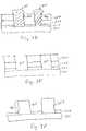
- FIGS. 1A-1Dillustrate a portion of the fabrication process for creating a tri-gate SOI transistor in accordance with the prior art.
- a carrier wafer 101typically a silicon substrate
- an insulator layer 102typically silicon dioxide, disposed upon it.
- a silicon dioxide layermay be grown on a silicon substrate.
- a transfer wafer 103is then bonded to the insulator layer 102 , which may facilitate the bonding.
- the bonding of the carrier wafer to the insulator layermay be effected though a heat-induced hydrogen bonding process.
- the transfer waferwhich may be, for example, silicon, is approximately 600 microns thick.
- the transfer waferis then thinned to a desired thickness based upon the transistor dimensions. Typically, this thickness is approximately 50-100 nm.
- the thinning of the transfer wafermay be accomplished through one of several typical processes. For example, a wet etch and polish process may be used to grind the transfer wafer to the desired thickness.
- An alternative method for thinning the transfer waferincludes hydrogen implantation of the transfer layer to create a weak section of the transfer wafer. The bonded pair is then heated to effect a high temperature cleave of the hydrogen-doped interface. Subsequently, the transfer wafer surface is polished or treated in other ways to planarize the surface or further reduce the thickness. These methods provide control of the thickness to within approximately several hundred angstroms. As shown in FIG.
- the transfer wafer 103has been thinned to a desired dimension for the silicon body of the transistor, resulting in film layer 104 .
- the thickness of film layer 104is determined by the desired height of the silicon body (H Si ).
- the film layer 104is then selectively etched to create silicon bodies for the transistors. As shown in FIG. 1D , selectively etching the film layer 104 , using lithography techniques, results in silicon bodies 105 having a desired body width (W Si ) and body height (H Si ).
- gate lengthis proportional to H Si , with H Si equal to about one-third of gate length.
- H Siis greater than approximately 20 nm.
- the H Si valuemust be uniform across a wafer in order to produce transistors with uniform characteristics.
- the transistor threshold voltagewhich is directly proportional to H Si , should not vary by more than approximately 10%. Therefore, the film layer thickness that determines H Si , should not vary by more than 10%.
- the methods of thinning the transfer layer to obtain the film layerare capable of producing a film layer of approximately 20 nm thickness that does not vary by more than approximately 10%. However, these methods fail to produce the required uniformity for thinner film layers. Therefore, current methods of fabricating SOI transistors are incapable of yielding transistors with gate lengths smaller than approximately 50 nm.
- FIGS. 1A-1Dillustrate a process for creating a tri-gate SOI transistor in accordance with the prior art
- FIG. 2illustrates a process for providing increased uniformity in silicon body height, H Si , in accordance with one embodiment of the invention.
- FIGS. 3A-3Gillustrate the fabrication of a tri-gate transistor in accordance with one embodiment of the invention.
- FIG. 2illustrates a process for providing increased uniformity in silicon body height, H Si , in accordance with one embodiment of the invention.
- Process 200shown in FIG. 2 , begins with operation 205 in which a trench layer is disposed upon a substrate layer.
- the trench layermay be disposed upon the substrate layer using a chemical vapor deposition (CVD) process.
- the substrate layeris silicon.
- the substrate layermay be another semiconductor material such as germanium (Ge) or gallium arsenide (GaAs).
- the trench layer thicknessis determined based upon the specification of the transistor's gate length. That is, the trench layer thickness is selected to be equal to a desired H Si value.
- the trench layeris a material that can be selectively etched using conventional etching processes.
- the trench layermay be multiple layers of different materials with each material. In one such embodiment, the multiple layers of the trench layer are susceptible to different etching processes.
- the trenches formed by operation 210are filled with a semiconductor material (e.g., silicon).
- a semiconductor materiale.g., silicon
- the trenchesare filled with epitaxial silicon using a selective epitaxial process.
- the trenchesare filled in some other manner.
- the trenchesmay be filled with polysilicon using a blanket deposition process.
- the excess semiconductor materialis removed. That is, semiconductor material filling the trench that extends above the surface of the remainder of the trench layer is removed.
- CMPchemical-mechanical polish
- the remainder of the trench layeris removed exposing semiconductor fins (i.e., the semiconductor material filling the trenches).
- semiconductor finsi.e., the semiconductor material filling the trenches.
- the height of the semiconductor finsis uniform to within less than 5%.
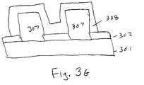
- FIGS. 3A-3Gillustrate the fabrication of a tri-gate transistor in accordance with one embodiment of the invention.
- FIG. 3Ashows a silicon substrate 301 .
- a multi-layer trench layeris disposed on the silicon substrate 301 .
- the trench layeris comprised of a first oxide (e.g., SiO 2 ) layer 302 , a nitride (e.g., Si 3 N 4 ) layer 303 , and a second oxide (e.g., SiO 2 ) layer 304 .
- a first oxidee.g., SiO 2
- a nitridee.g., Si 3 N 4
- a second oxidee.g., SiO 2
- FIG. 3Billustrates the application of a photoresist mask layer 305 to define the transistor bodies.
- the patterning of the photoresist mask layer 305determines the width of the silicon body, W Si .
- FIG. 3Cillustrates the etching of the trench layer to define trenches 306 a and 306 b .
- a series of three distinct dry etch processesare employed.
- the second oxide layer 304is etched using a selective dry etch process in which the nitride layer 303 acts as an etch stop.
- the nitride layer 303is etched using a different selective dry etch process in which the first oxide layer 302 acts as an etch stop.
- the first oxide layer 302is etched using a dry etch process that is sufficiently selective to stop on the surface of the silicon substrate 301 .
- FIG. 3Dillustrates filling trenches 306 a and 306 b with silicon 307 after the photoresist layer 305 has been stripped away, as indicated.
- the trenchesmay be filled with silicon through various alternative methods including epitaxial growth or blanket deposition of polysilicon.
- FIG. 3Eillustrates the silicon 307 planarized to the level of the second oxide layer 304 .
- the planarizationis effected using a CMP process.
- the polishing processis used to remove the second oxide layer 304 and the nitride layer 303 is used as a polish stop.
- the polishhas a high selectivity between oxide and nitride.
- the second oxide layer 304is selectively etched to the nitride layer 303 .
- the nitride layer 303is etched using a wet etch process using, for example, phosphoric acid.
- the first oxide layer 302acts as an etch stop for such a process.
- FIG. 3Fillustrates the silicon bodies for the tri-gate transistors exposed with the removal of the trench layer (e.g., second oxide layer 304 and the nitride layer 303 ). As shown in FIG. 3F , a portion of the trench layer (e.g., first oxide layer 302 ) may be retained to effect beneficial properties of the transistor as explained below.
- the silicon 307 forming the gate bodieshas a uniform height to within a specified tolerance. For one embodiment, the height, H Si , of silicon 307 is approximately 10 nm and is uniform within 5%.
- FIG. 3Gillustrates the tri-gate transistor fabricated by forming a gate 308 surrounding the silicon 307 .
- the gate 308may be, for example, metal or another suitable material as known in the art.
- Embodiments of the inventioninclude various operations. Many of the methods are described in their most basic form, but operations can be added to or deleted from any of the methods without departing from the basic scope of the invention.
- the trench layerdescribed in operation 205 of FIG. 2 , may be disposed on the substrate in various alternative matters and may be comprised of more than one layer as illustrated in FIG. 3A . Furthermore, a portion of the trench layer may be retained to effect benefits. As shown in FIGS. 3F and 3G , a portion of the first oxide layer is retained to reduce fringe capacitance in the transistor.
- the trenches formed in the trench layermay be filled with silicon in a number of ways including, for example, blanket deposition of polysilicon.
- a blanket deposition of polysiliconis used, an annealing process is employed after deposition to anneal the silicon into a single crystal.
Landscapes
- Thin Film Transistor (AREA)
- Element Separation (AREA)
- Insulated Gate Type Field-Effect Transistor (AREA)
Abstract
Description
- Embodiments of the invention relate generally to the field of integrated circuit device fabrication and more specifically to tri-gate transistor fabrication.
- The trend toward increasing the number of functions of an integrated circuit device (IC device) is continuing. As the size of transistors decreases, serious drawbacks in current transistor fabrication processes become evident. For example, typical silicon-on-insulator (SOI) transistors are fabricated by coating a substrate with an insulator (e.g., glass or silicon oxide) layer. A second silicon wafer is then bonded to the insulator layer and thinned to a desired thickness (i.e., as determined by the transistor dimensions). This thinning process is very difficult to control with great accuracy.
FIGS. 1A-1D illustrate a portion of the fabrication process for creating a tri-gate SOI transistor in accordance with the prior art. As shown inFIG. 1A , acarrier wafer 101, typically a silicon substrate, has aninsulator layer 102, typically silicon dioxide, disposed upon it. For example, a silicon dioxide layer may be grown on a silicon substrate.- As shown in
FIG. 1B , a transfer wafer103 is then bonded to theinsulator layer 102, which may facilitate the bonding. The bonding of the carrier wafer to the insulator layer may be effected though a heat-induced hydrogen bonding process. The transfer wafer, which may be, for example, silicon, is approximately 600 microns thick. - The transfer wafer is then thinned to a desired thickness based upon the transistor dimensions. Typically, this thickness is approximately 50-100 nm. The thinning of the transfer wafer may be accomplished through one of several typical processes. For example, a wet etch and polish process may be used to grind the transfer wafer to the desired thickness. An alternative method for thinning the transfer wafer includes hydrogen implantation of the transfer layer to create a weak section of the transfer wafer. The bonded pair is then heated to effect a high temperature cleave of the hydrogen-doped interface. Subsequently, the transfer wafer surface is polished or treated in other ways to planarize the surface or further reduce the thickness. These methods provide control of the thickness to within approximately several hundred angstroms. As shown in
FIG. 1C , the transfer wafer103 has been thinned to a desired dimension for the silicon body of the transistor, resulting in film layer104. The thickness of film layer104 is determined by the desired height of the silicon body (HSi). The film layer104 is then selectively etched to create silicon bodies for the transistors. As shown inFIG. 1D , selectively etching the film layer104, using lithography techniques, results insilicon bodies 105 having a desired body width (WSi) and body height (HSi). - For typical transistor design architecture, gate length is proportional to HSi, with HSiequal to about one-third of gate length. For typical transistors with gate lengths of approximately 20-100 nm, the desired HSiis greater than approximately 20 nm. Using the current fabrication method, it is possible to create adequate film layers. However, as the gate length, and hence, the desired HSidecreases, current fabrication methods exhibit serious disadvantages.
- The HSivalue must be uniform across a wafer in order to produce transistors with uniform characteristics. For example, the transistor threshold voltage, which is directly proportional to HSi, should not vary by more than approximately 10%. Therefore, the film layer thickness that determines HSi, should not vary by more than 10%.
- The methods of thinning the transfer layer to obtain the film layer are capable of producing a film layer of approximately 20 nm thickness that does not vary by more than approximately 10%. However, these methods fail to produce the required uniformity for thinner film layers. Therefore, current methods of fabricating SOI transistors are incapable of yielding transistors with gate lengths smaller than approximately 50 nm.
- Moreover, the process of bonding the carrier wafer and transfer wafer, and the process of thinning the transfer wafer to the desired thickness, are costly and difficult to control.
- The invention may be best understood by referring to the following description and accompanying drawings that are used to illustrate embodiments of the invention. In the drawings:
FIGS. 1A-1D illustrate a process for creating a tri-gate SOI transistor in accordance with the prior art;FIG. 2 illustrates a process for providing increased uniformity in silicon body height, HSi, in accordance with one embodiment of the invention; andFIGS. 3A-3G illustrate the fabrication of a tri-gate transistor in accordance with one embodiment of the invention.- In the following description, numerous specific details are set forth. However, it is understood that embodiments of the invention may be practiced without these specific details. In other instances, well-known circuits, structures and techniques have not been shown in detail in order not to obscure the understanding of this description.
- Reference throughout the specification to “one embodiment” or “an embodiment” means that a particular feature, structure, or characteristic described in connection with the embodiment is included in at least one embodiment of the present invention. Thus, the appearance of the phrases “in one embodiment” or “in an embodiment” in various places throughout the specification are not necessarily all referring to the same embodiment. Furthermore, the particular features, structures, or characteristics may be combined in any suitable manner in one or more embodiments.
- Moreover, inventive aspects lie in less than all features of a single disclosed embodiment. Thus, the claims following the Detailed Description are hereby expressly incorporated into this Detailed Description, with each claim standing on its own as a separate embodiment of this invention.
FIG. 2 illustrates a process for providing increased uniformity in silicon body height, HSi, in accordance with one embodiment of the invention. Process200, shown inFIG. 2 , begins withoperation 205 in which a trench layer is disposed upon a substrate layer. For one embodiment, the trench layer may be disposed upon the substrate layer using a chemical vapor deposition (CVD) process. For one embodiment, the substrate layer is silicon. For alternative embodiments, the substrate layer may be another semiconductor material such as germanium (Ge) or gallium arsenide (GaAs). For one embodiment, the trench layer thickness is determined based upon the specification of the transistor's gate length. That is, the trench layer thickness is selected to be equal to a desired HSivalue.- At
operation 210, selected portions of the trench layer are removed, thus forming trenches. For one embodiment, the trench layer is a material that can be selectively etched using conventional etching processes. For various alternative embodiments, the trench layer may be multiple layers of different materials with each material. In one such embodiment, the multiple layers of the trench layer are susceptible to different etching processes. - At
operation 215, the trenches formed byoperation 210, are filled with a semiconductor material (e.g., silicon). For one embodiment, the trenches are filled with epitaxial silicon using a selective epitaxial process. In an alternative embodiment, the trenches are filled in some other manner. For example, the trenches may be filled with polysilicon using a blanket deposition process. - At
operation 220, the excess semiconductor material is removed. That is, semiconductor material filling the trench that extends above the surface of the remainder of the trench layer is removed. For one embodiment, a chemical-mechanical polish (CMP) is employed to planarize the surface of the semiconductor material. - At
operation 225, the remainder of the trench layer is removed exposing semiconductor fins (i.e., the semiconductor material filling the trenches). For one embodiment, the height of the semiconductor fins is uniform to within less than 5%. FIGS. 3A-3G illustrate the fabrication of a tri-gate transistor in accordance with one embodiment of the invention.FIG. 3A shows asilicon substrate 301. A multi-layer trench layer is disposed on thesilicon substrate 301. The trench layer is comprised of a first oxide (e.g., SiO2)layer 302, a nitride (e.g., Si3N4)layer 303, and a second oxide (e.g., SiO2)layer 304. Eventually the tri-gate body thickness, HSi, will be determined by the thickness of the second oxide layer, which is a very controllable thickness.FIG. 3B illustrates the application of aphotoresist mask layer 305 to define the transistor bodies. The patterning of thephotoresist mask layer 305 determines the width of the silicon body, WSi.FIG. 3C illustrates the etching of the trench layer to define trenches306aand306b. For one embodiment, a series of three distinct dry etch processes are employed. In such an embodiment, thesecond oxide layer 304 is etched using a selective dry etch process in which thenitride layer 303 acts as an etch stop. Then thenitride layer 303 is etched using a different selective dry etch process in which thefirst oxide layer 302 acts as an etch stop. Finally, thefirst oxide layer 302 is etched using a dry etch process that is sufficiently selective to stop on the surface of thesilicon substrate 301.FIG. 3D illustrates filling trenches306aand306bwithsilicon 307 after thephotoresist layer 305 has been stripped away, as indicated. As noted above, the trenches may be filled with silicon through various alternative methods including epitaxial growth or blanket deposition of polysilicon.FIG. 3E illustrates thesilicon 307 planarized to the level of thesecond oxide layer 304. For one embodiment, the planarization is effected using a CMP process. For one embodiment, the polishing process is used to remove thesecond oxide layer 304 and thenitride layer 303 is used as a polish stop. For such an embodiment, the polish has a high selectivity between oxide and nitride. For an alternative embodiment, thesecond oxide layer 304 is selectively etched to thenitride layer 303. Subsequently, thenitride layer 303 is etched using a wet etch process using, for example, phosphoric acid. Thefirst oxide layer 302 acts as an etch stop for such a process.FIG. 3F illustrates the silicon bodies for the tri-gate transistors exposed with the removal of the trench layer (e.g.,second oxide layer 304 and the nitride layer303). As shown inFIG. 3F , a portion of the trench layer (e.g., first oxide layer302) may be retained to effect beneficial properties of the transistor as explained below. Thesilicon 307 forming the gate bodies has a uniform height to within a specified tolerance. For one embodiment, the height, HSi, ofsilicon 307 is approximately 10 nm and is uniform within 5%.FIG. 3G illustrates the tri-gate transistor fabricated by forming agate 308 surrounding thesilicon 307. Thegate 308 may be, for example, metal or another suitable material as known in the art.- General Matters
- Embodiments of the invention include various operations. Many of the methods are described in their most basic form, but operations can be added to or deleted from any of the methods without departing from the basic scope of the invention. For example, the trench layer, described in
operation 205 ofFIG. 2 , may be disposed on the substrate in various alternative matters and may be comprised of more than one layer as illustrated inFIG. 3A . Furthermore, a portion of the trench layer may be retained to effect benefits. As shown inFIGS. 3F and 3G , a portion of the first oxide layer is retained to reduce fringe capacitance in the transistor. - As described above, the trenches formed in the trench layer may be filled with silicon in a number of ways including, for example, blanket deposition of polysilicon. For an embodiment in which a blanket deposition of polysilicon is used, an annealing process is employed after deposition to anneal the silicon into a single crystal.
- While the invention has been described in terms of several embodiments, those skilled in the art will recognize that the invention is not limited to the embodiments described, but can be practiced with modification and alteration within the spirit and scope of the appended claims. The description is thus to be regarded as illustrative instead of limiting.
Claims (23)
1. A method comprising:
disposing a trench layer upon a semiconductor substrate;
selectively removing a portion of the trench layer such that a remainder of the trench layer forms one or more trenches, the removal of a portion of the trench layer exposing the semiconductor substrate;
filling the one or more trenches with a semiconductor material;
removing any excess semiconductor material from the one or more trenches; and
removing an additional portion of the trench layer to expose the semiconductor material as one or more semiconductor fins.
2. The method ofclaim 1 wherein the trench layer is comprised of a plurality of layers.
3. The method ofclaim 2 wherein the plurality of layers include a first oxide layer disposed upon the semiconductor substrate, a nitride layer disposed upon the first oxide layer, and a second oxide layer disposed upon the nitride layer.
4. The method ofclaim 3 wherein removing an additional portion of the trench layer comprises removing any remaining portion of the second oxide layer, any remaining portion of the nitride layer, and retaining at least some portion of any remaining portion of the first oxide layer.
5. The method ofclaim 1 wherein the one or more trenches have a depth of approximately 10 nm.
6. The method ofclaim 5 wherein the one or more semiconductor fins have a height of approximately 10 nm that is uniform to within 5%.
7. The method ofclaim 1 wherein removing any excess semiconductor material from the one or more trenches includes planarizing the semiconductor material to a surface of the trench layer.
8. The method ofclaim 7 wherein the planarizing is effected through a chemical-mechanical polishing process.
9. The method ofclaim 1 wherein filling the one or more trenches with a semiconductor material includes epitaxially growing the semiconductor material within the one or more trenches.
10. The method ofclaim 1 wherein filling the one or more trenches with a semiconductor material includes a blanket deposition of semiconductor material.
11. An integrated circuit device comprising:
a substrate; and
one or more transistors formed upon the substrate, each transistor having a semiconductor body, each semiconductor body having a height of less than 20 nm, the height of each semiconductor body uniform to within a tolerance of 5% of a specified height.
12. The integrated circuit device ofclaim 11 wherein the one or more transistors are tri-gate transistors.
13. The integrated circuit device ofclaim 12 wherein each semiconductor body has a height of approximately 10 nm.
14. A method comprising:
disposing a first oxide layer on a semiconductor substrate;
disposing a nitride layer upon the first oxide layer;
disposing a second oxide layer upon the nitride layer;
selectively etching a portion of the second oxide layer and the nitride layer to define one or more trenches;
filling the one or more trenches with a semiconductor material;
removing the excess semiconductor material from the one or more trenches; and
selectively etching a remainder of the second oxide layer and the nitride layer such that one or more semiconductor bodies are formed.
15. The method ofclaim 14 wherein the one or more trenches have a depth of approximately 10 nm.
16. The method ofclaim 14 wherein the one or more semiconductor bodies have a height of less than 20 nm that is uniform to within 5%.
17. The method ofclaim 16 wherein the one or more semiconductor bodies have a height of approximately 10 nm.
18. The method ofclaim 14 wherein removing any excess semiconductor material from the one or more trenches includes planarizing the semiconductor material to a surface of the second oxide layer.
19. The method ofclaim 18 wherein the planarizing is effected through a chemical-mechanical polishing process.
20. The method ofclaim 14 wherein filling the one or more trenches with a semiconductor material includes epitaxially growing the semiconductor material within the one or more trenches.
21. The method ofclaim 14 wherein filling the one or more trenches with a semiconductor material includes a blanket deposition of semiconductor material.
22. The method ofclaim 14 wherein the semiconductor substrate is comprised of a semiconductor material selected from the group consisting of silicon, germanium, and gallium arsenide.
23. The method ofclaim 14 wherein the semiconductor substrate is comprised of silicon, the first oxide layer is comprised of SiO2, the nitride layer is comprised of Si3N4, and the second oxide layer is comprised of SiO2.
Priority Applications (7)
| Application Number | Priority Date | Filing Date | Title |
|---|---|---|---|
| US10/760,028US7268058B2 (en) | 2004-01-16 | 2004-01-16 | Tri-gate transistors and methods to fabricate same |
| JP2006549560AJP2007521667A (en) | 2004-01-16 | 2005-01-10 | Tri-gate transistor and manufacturing method thereof |
| EP05711376AEP1704590A1 (en) | 2004-01-16 | 2005-01-10 | Tri-gate transistors and mehtods to fabricate same |
| CNB2005800072795ACN100550324C (en) | 2004-01-16 | 2005-01-10 | Tri-gate transistors and manufacture method thereof |
| PCT/US2005/000947WO2005071730A1 (en) | 2004-01-16 | 2005-01-10 | Tri-gate transistors and mehtods to fabricate same |
| TW094101018ATWI297212B (en) | 2004-01-16 | 2005-01-13 | Tri-gate transistors and methods to fabricate same |
| US11/828,290US20070262389A1 (en) | 2004-01-16 | 2007-07-25 | Tri-gate transistors and methods to fabricate same |
Applications Claiming Priority (1)
| Application Number | Priority Date | Filing Date | Title |
|---|---|---|---|
| US10/760,028US7268058B2 (en) | 2004-01-16 | 2004-01-16 | Tri-gate transistors and methods to fabricate same |
Related Child Applications (1)
| Application Number | Title | Priority Date | Filing Date |
|---|---|---|---|
| US11/828,290DivisionUS20070262389A1 (en) | 2004-01-16 | 2007-07-25 | Tri-gate transistors and methods to fabricate same |
Publications (2)
| Publication Number | Publication Date |
|---|---|
| US20050158970A1true US20050158970A1 (en) | 2005-07-21 |
| US7268058B2 US7268058B2 (en) | 2007-09-11 |
Family
ID=34749835
Family Applications (2)
| Application Number | Title | Priority Date | Filing Date |
|---|---|---|---|
| US10/760,028Expired - LifetimeUS7268058B2 (en) | 2004-01-16 | 2004-01-16 | Tri-gate transistors and methods to fabricate same |
| US11/828,290AbandonedUS20070262389A1 (en) | 2004-01-16 | 2007-07-25 | Tri-gate transistors and methods to fabricate same |
Family Applications After (1)
| Application Number | Title | Priority Date | Filing Date |
|---|---|---|---|
| US11/828,290AbandonedUS20070262389A1 (en) | 2004-01-16 | 2007-07-25 | Tri-gate transistors and methods to fabricate same |
Country Status (6)
| Country | Link |
|---|---|
| US (2) | US7268058B2 (en) |
| EP (1) | EP1704590A1 (en) |
| JP (1) | JP2007521667A (en) |
| CN (1) | CN100550324C (en) |
| TW (1) | TWI297212B (en) |
| WO (1) | WO2005071730A1 (en) |
Cited By (9)
| Publication number | Priority date | Publication date | Assignee | Title |
|---|---|---|---|---|
| US20070145487A1 (en)* | 2005-12-27 | 2007-06-28 | Intel Corporation | Multigate device with recessed strain regions |
| US20070257325A1 (en)* | 2006-05-03 | 2007-11-08 | Willy Rachmady | Tri-gate device with conformal PVD workfunction metal on its three-dimensional body and fabrication method thereof |
| US20080164531A1 (en)* | 2007-01-04 | 2008-07-10 | Freescale Semiconductor, Inc. | Dual interlayer dielectric stressor integration with a sacrificial underlayer film stack |
| WO2013155332A1 (en)* | 2012-04-13 | 2013-10-17 | SanDisk Technologies, Inc. | Thin film transistor |
| CN103578995A (en)* | 2012-07-27 | 2014-02-12 | 中芯国际集成电路制造(上海)有限公司 | Method for forming FinFET |
| CN103887177A (en)* | 2014-03-27 | 2014-06-25 | 上海集成电路研发中心有限公司 | Finned active area manufacturing method |
| US20150270341A1 (en)* | 2012-10-18 | 2015-09-24 | Institute of Microelectronics, Chinese Academy of Sciences | Method for manufacturing fin structure of finfet |
| US9165933B2 (en) | 2013-03-07 | 2015-10-20 | Sandisk 3D Llc | Vertical bit line TFT decoder for high voltage operation |
| US9240420B2 (en) | 2013-09-06 | 2016-01-19 | Sandisk Technologies Inc. | 3D non-volatile storage with wide band gap transistor decoder |
Families Citing this family (84)
| Publication number | Priority date | Publication date | Assignee | Title |
|---|---|---|---|---|
| US6909151B2 (en) | 2003-06-27 | 2005-06-21 | Intel Corporation | Nonplanar device with stress incorporation layer and method of fabrication |
| US7456476B2 (en) | 2003-06-27 | 2008-11-25 | Intel Corporation | Nonplanar semiconductor device with partially or fully wrapped around gate electrode and methods of fabrication |
| US7154118B2 (en) | 2004-03-31 | 2006-12-26 | Intel Corporation | Bulk non-planar transistor having strained enhanced mobility and methods of fabrication |
| US7042009B2 (en) | 2004-06-30 | 2006-05-09 | Intel Corporation | High mobility tri-gate devices and methods of fabrication |
| US7348284B2 (en) | 2004-08-10 | 2008-03-25 | Intel Corporation | Non-planar pMOS structure with a strained channel region and an integrated strained CMOS flow |
| US7422946B2 (en) | 2004-09-29 | 2008-09-09 | Intel Corporation | Independently accessed double-gate and tri-gate transistors in same process flow |
| US20060086977A1 (en) | 2004-10-25 | 2006-04-27 | Uday Shah | Nonplanar device with thinned lower body portion and method of fabrication |
| US7518196B2 (en) | 2005-02-23 | 2009-04-14 | Intel Corporation | Field effect transistor with narrow bandgap source and drain regions and method of fabrication |
| US20060202266A1 (en) | 2005-03-14 | 2006-09-14 | Marko Radosavljevic | Field effect transistor with metal source/drain regions |
| US8324660B2 (en) | 2005-05-17 | 2012-12-04 | Taiwan Semiconductor Manufacturing Company, Ltd. | Lattice-mismatched semiconductor structures with reduced dislocation defect densities and related methods for device fabrication |
| US9153645B2 (en) | 2005-05-17 | 2015-10-06 | Taiwan Semiconductor Manufacturing Company, Ltd. | Lattice-mismatched semiconductor structures with reduced dislocation defect densities and related methods for device fabrication |
| US7858481B2 (en) | 2005-06-15 | 2010-12-28 | Intel Corporation | Method for fabricating transistor with thinned channel |
| US7547637B2 (en) | 2005-06-21 | 2009-06-16 | Intel Corporation | Methods for patterning a semiconductor film |
| US7279375B2 (en) | 2005-06-30 | 2007-10-09 | Intel Corporation | Block contact architectures for nanoscale channel transistors |
| KR101329388B1 (en) | 2005-07-26 | 2013-11-14 | 앰버웨이브 시스템즈 코포레이션 | Solutions for integrated circuit integration of alternative active area materials |
| US7402875B2 (en) | 2005-08-17 | 2008-07-22 | Intel Corporation | Lateral undercut of metal gate in SOI device |
| US20070054467A1 (en)* | 2005-09-07 | 2007-03-08 | Amberwave Systems Corporation | Methods for integrating lattice-mismatched semiconductor structure on insulators |
| US7638842B2 (en) | 2005-09-07 | 2009-12-29 | Amberwave Systems Corporation | Lattice-mismatched semiconductor structures on insulators |
| US20070090416A1 (en) | 2005-09-28 | 2007-04-26 | Doyle Brian S | CMOS devices with a single work function gate electrode and method of fabrication |
| US7479421B2 (en) | 2005-09-28 | 2009-01-20 | Intel Corporation | Process for integrating planar and non-planar CMOS transistors on a bulk substrate and article made thereby |
| US7485503B2 (en) | 2005-11-30 | 2009-02-03 | Intel Corporation | Dielectric interface for group III-V semiconductor device |
| WO2007112066A2 (en) | 2006-03-24 | 2007-10-04 | Amberwave Systems Corporation | Lattice-mismatched semiconductor structures and related methods for device fabrication |
| JP2007299991A (en)* | 2006-05-01 | 2007-11-15 | Toshiba Corp | Semiconductor device and manufacturing method thereof |
| US7517764B2 (en)* | 2006-06-29 | 2009-04-14 | International Business Machines Corporation | Bulk FinFET device |
| KR100801078B1 (en)* | 2006-06-29 | 2008-02-11 | 삼성전자주식회사 | Non-volatile memory integrated circuit device having a vertical channel and its manufacturing method |
| US8143646B2 (en) | 2006-08-02 | 2012-03-27 | Intel Corporation | Stacking fault and twin blocking barrier for integrating III-V on Si |
| US8173551B2 (en)* | 2006-09-07 | 2012-05-08 | Taiwan Semiconductor Manufacturing Co., Ltd. | Defect reduction using aspect ratio trapping |
| WO2008039495A1 (en) | 2006-09-27 | 2008-04-03 | Amberwave Systems Corporation | Tri-gate field-effect transistors formed by aspect ratio trapping |
| WO2008039534A2 (en) | 2006-09-27 | 2008-04-03 | Amberwave Systems Corporation | Quantum tunneling devices and circuits with lattice- mismatched semiconductor structures |
| US8502263B2 (en) | 2006-10-19 | 2013-08-06 | Taiwan Semiconductor Manufacturing Company, Ltd. | Light-emitter-based devices with lattice-mismatched semiconductor structures |
| WO2008124154A2 (en) | 2007-04-09 | 2008-10-16 | Amberwave Systems Corporation | Photovoltaics on silicon |
| US8304805B2 (en) | 2009-01-09 | 2012-11-06 | Taiwan Semiconductor Manufacturing Company, Ltd. | Semiconductor diodes fabricated by aspect ratio trapping with coalesced films |
| US7825328B2 (en) | 2007-04-09 | 2010-11-02 | Taiwan Semiconductor Manufacturing Company, Ltd. | Nitride-based multi-junction solar cell modules and methods for making the same |
| US8237151B2 (en) | 2009-01-09 | 2012-08-07 | Taiwan Semiconductor Manufacturing Company, Ltd. | Diode-based devices and methods for making the same |
| US8329541B2 (en) | 2007-06-15 | 2012-12-11 | Taiwan Semiconductor Manufacturing Company, Ltd. | InP-based transistor fabrication |
| JP2010538495A (en) | 2007-09-07 | 2010-12-09 | アンバーウェーブ・システムズ・コーポレーション | Multi-junction solar cell |
| US7763943B2 (en)* | 2007-12-26 | 2010-07-27 | Intel Corporation | Reducing external resistance of a multi-gate device by incorporation of a partial metallic fin |
| US8030163B2 (en)* | 2007-12-26 | 2011-10-04 | Intel Corporation | Reducing external resistance of a multi-gate device using spacer processing techniques |
| US20090206404A1 (en)* | 2008-02-15 | 2009-08-20 | Ravi Pillarisetty | Reducing external resistance of a multi-gate device by silicidation |
| US8129749B2 (en)* | 2008-03-28 | 2012-03-06 | Intel Corporation | Double quantum well structures for transistors |
| US8278687B2 (en)* | 2008-03-28 | 2012-10-02 | Intel Corporation | Semiconductor heterostructures to reduce short channel effects |
| US7800166B2 (en)* | 2008-05-30 | 2010-09-21 | Intel Corporation | Recessed channel array transistor (RCAT) structures and method of formation |
| US8183667B2 (en) | 2008-06-03 | 2012-05-22 | Taiwan Semiconductor Manufacturing Co., Ltd. | Epitaxial growth of crystalline material |
| US8362566B2 (en) | 2008-06-23 | 2013-01-29 | Intel Corporation | Stress in trigate devices using complimentary gate fill materials |
| US8274097B2 (en) | 2008-07-01 | 2012-09-25 | Taiwan Semiconductor Manufacturing Company, Ltd. | Reduction of edge effects from aspect ratio trapping |
| US8981427B2 (en) | 2008-07-15 | 2015-03-17 | Taiwan Semiconductor Manufacturing Company, Ltd. | Polishing of small composite semiconductor materials |
| US7833891B2 (en)* | 2008-07-23 | 2010-11-16 | International Business Machines Corporation | Semiconductor device manufacturing method using oxygen diffusion barrier layer between buried oxide layer and high K dielectric layer |
| US7884354B2 (en)* | 2008-07-31 | 2011-02-08 | Intel Corporation | Germanium on insulator (GOI) semiconductor substrates |
| US7781283B2 (en)* | 2008-08-15 | 2010-08-24 | International Business Machines Corporation | Split-gate DRAM with MuGFET, design structure, and method of manufacture |
| US7979836B2 (en)* | 2008-08-15 | 2011-07-12 | International Business Machines Corporation | Split-gate DRAM with MuGFET, design structure, and method of manufacture |
| EP2335273A4 (en) | 2008-09-19 | 2012-01-25 | Taiwan Semiconductor Mfg | FORMATION OF DEVICES BY GROWTH OF EPITAXIAL LAYERS |
| US20100072515A1 (en) | 2008-09-19 | 2010-03-25 | Amberwave Systems Corporation | Fabrication and structures of crystalline material |
| US8253211B2 (en) | 2008-09-24 | 2012-08-28 | Taiwan Semiconductor Manufacturing Company, Ltd. | Semiconductor sensor structures with reduced dislocation defect densities |
| US8184472B2 (en)* | 2009-03-13 | 2012-05-22 | International Business Machines Corporation | Split-gate DRAM with lateral control-gate MuGFET |
| US8629446B2 (en) | 2009-04-02 | 2014-01-14 | Taiwan Semiconductor Manufacturing Company, Ltd. | Devices formed from a non-polar plane of a crystalline material and method of making the same |
| US8440998B2 (en) | 2009-12-21 | 2013-05-14 | Intel Corporation | Increasing carrier injection velocity for integrated circuit devices |
| US8633470B2 (en)* | 2009-12-23 | 2014-01-21 | Intel Corporation | Techniques and configurations to impart strain to integrated circuit devices |
| US8313995B2 (en)* | 2011-01-13 | 2012-11-20 | Infineon Technologies Austria Ag | Method for manufacturing a semiconductor device |
| US9105660B2 (en) | 2011-08-17 | 2015-08-11 | United Microelectronics Corp. | Fin-FET and method of forming the same |
| CN102956466B (en)* | 2011-08-26 | 2016-11-16 | 联华电子股份有限公司 | Fin transistor and method for making same |
| CN103137445B (en)* | 2011-12-05 | 2015-12-02 | 中芯国际集成电路制造(上海)有限公司 | Form the method for Finfet doping fin |
| CN103177948B (en)* | 2011-12-22 | 2015-11-25 | 中芯国际集成电路制造(上海)有限公司 | The fin of fin field effect pipe and the formation method of fin field effect pipe |
| US9082746B2 (en)* | 2012-01-16 | 2015-07-14 | Infineon Technologies Austria Ag | Method for forming self-aligned trench contacts of semiconductor components and a semiconductor component |
| US20130302954A1 (en)* | 2012-05-10 | 2013-11-14 | Globalfoundries Inc. | Methods of forming fins for a finfet device without performing a cmp process |
| CN103515234B (en)* | 2012-06-25 | 2016-12-21 | 中芯国际集成电路制造(上海)有限公司 | The method forming FinFET |
| US9142400B1 (en) | 2012-07-17 | 2015-09-22 | Stc.Unm | Method of making a heteroepitaxial layer on a seed area |
| US8765563B2 (en) | 2012-09-28 | 2014-07-01 | Intel Corporation | Trench confined epitaxially grown device layer(s) |
| CN103811324B (en)* | 2012-11-13 | 2016-08-31 | 中芯国际集成电路制造(上海)有限公司 | The forming method of fin field effect pipe |
| US8768271B1 (en) | 2012-12-19 | 2014-07-01 | Intel Corporation | Group III-N transistors on nanoscale template structures |
| CN104037085A (en)* | 2013-03-07 | 2014-09-10 | 中国科学院微电子研究所 | Semiconductor device manufacturing method |
| US8987082B2 (en) | 2013-05-31 | 2015-03-24 | Stmicroelectronics, Inc. | Method of making a semiconductor device using sacrificial fins |
| US20140353716A1 (en) | 2013-05-31 | 2014-12-04 | Stmicroelectronics, Inc | Method of making a semiconductor device using a dummy gate |
| US9082788B2 (en) | 2013-05-31 | 2015-07-14 | Stmicroelectronics, Inc. | Method of making a semiconductor device including an all around gate |
| CN104347409B (en)* | 2013-07-24 | 2017-11-28 | 中芯国际集成电路制造(上海)有限公司 | The forming method of semiconductor structure |
| US9105582B2 (en) | 2013-08-15 | 2015-08-11 | United Microelectronics Corporation | Spatial semiconductor structure and method of fabricating the same |
| US9018711B1 (en)* | 2013-10-17 | 2015-04-28 | Globalfoundries Inc. | Selective growth of a work-function metal in a replacement metal gate of a semiconductor device |
| US20150380258A1 (en)* | 2014-06-25 | 2015-12-31 | Stmicroelectronics, Inc. | Method for controlling height of a fin structure |
| CN105428413B (en)* | 2014-07-24 | 2019-01-22 | 中芯国际集成电路制造(上海)有限公司 | Fin field effect pipe and forming method thereof |
| US9312143B1 (en) | 2014-11-24 | 2016-04-12 | International Business Machines Corporation | Formation of isolation surrounding well implantation |
| US9530701B2 (en) | 2014-12-18 | 2016-12-27 | International Business Machines Corporation | Method of forming semiconductor fins on SOI substrate |
| US20170018427A1 (en)* | 2015-07-15 | 2017-01-19 | Applied Materials, Inc. | Method of selective epitaxy |
| US9397005B1 (en)* | 2015-07-20 | 2016-07-19 | International Business Machines Corporation | Dual-material mandrel for epitaxial crystal growth on silicon |
| CN107039519B (en)* | 2016-02-03 | 2019-12-03 | 中芯国际集成电路制造(上海)有限公司 | Fin formula field effect transistor and forming method thereof |
| US10121675B2 (en) | 2016-12-29 | 2018-11-06 | Taiwan Semiconductor Manufacturing Co., Ltd | Semiconductor device and a method for fabricating the same |
Citations (93)
| Publication number | Priority date | Publication date | Assignee | Title |
|---|---|---|---|---|
| US4906589A (en)* | 1989-02-06 | 1990-03-06 | Industrial Technology Research Institute | Inverse-T LDDFET with self-aligned silicide |
| US4996574A (en)* | 1988-07-01 | 1991-02-26 | Fujitsu Limited | MIS transistor structure for increasing conductance between source and drain regions |
| US5124777A (en)* | 1990-07-02 | 1992-06-23 | Samsung Electronics Co., Ltd. | Dielectric medium for capacitor of semiconductor device |
| US5338959A (en)* | 1992-03-30 | 1994-08-16 | Samsung Electronics Co., Ltd. | Thin film transistor with three dimensional multichannel structure |
| US5391506A (en)* | 1992-01-31 | 1995-02-21 | Kawasaki Steel Corporation | Manufacturing method for semiconductor devices with source/drain formed in substrate projection. |
| US5521859A (en)* | 1991-03-20 | 1996-05-28 | Fujitsu Limited | Semiconductor memory device having thin film transistor and method of producing the same |
| US5543351A (en)* | 1992-03-19 | 1996-08-06 | Matsushita Electric Industrial Co., Ltd. | Method of producing electrically insulated silicon structure |
| US5545586A (en)* | 1990-11-27 | 1996-08-13 | Nec Corporation | Method of making a transistor having easily controllable impurity profile |
| US5658806A (en)* | 1995-10-26 | 1997-08-19 | National Science Council | Method for fabricating thin-film transistor with bottom-gate or dual-gate configuration |
| US5716879A (en)* | 1994-12-15 | 1998-02-10 | Goldstar Electron Company, Ltd. | Method of making a thin film transistor |
| US5739544A (en)* | 1993-05-26 | 1998-04-14 | Matsushita Electric Industrial Co., Ltd. | Quantization functional device utilizing a resonance tunneling effect and method for producing the same |
| US5888309A (en)* | 1997-12-29 | 1999-03-30 | Taiwan Semiconductor Manufacturing Company, Ltd. | Lateral etch inhibited multiple for forming a via through a microelectronics layer susceptible to etching within a fluorine containing plasma followed by an oxygen containing plasma |
| US5899710A (en)* | 1995-01-20 | 1999-05-04 | Sony Corporation | Method for forming field effect transistor having multiple gate electrodes surrounding the channel region |
| US5905285A (en)* | 1996-09-12 | 1999-05-18 | Advanced Micro Devices, Inc. | Ultra short trench transistors and process for making same |
| US6018176A (en)* | 1995-05-26 | 2000-01-25 | Samsung Electronics Co., Ltd. | Vertical transistor and memory cell |
| US6066869A (en)* | 1997-10-06 | 2000-05-23 | Micron Technology, Inc. | Circuit and method for a folded bit line memory cell with vertical transistor and trench capacitor |
| US6190975B1 (en)* | 1996-09-17 | 2001-02-20 | Matsushita Electric Industrial Co., Ltd. | Method of forming HCMOS devices with a silicon-germanium-carbon compound semiconductor layer |
| US6252284B1 (en)* | 1999-12-09 | 2001-06-26 | International Business Machines Corporation | Planarized silicon fin device |
| US6259135B1 (en)* | 1999-09-24 | 2001-07-10 | International Business Machines Corporation | MOS transistors structure for reducing the size of pitch limited circuits |
| US20020011612A1 (en)* | 2000-07-31 | 2002-01-31 | Kabushiki Kaisha Toshiba | Semiconductor device and method for manufacturing the same |
| US6359311B1 (en)* | 2001-01-17 | 2002-03-19 | Taiwan Semiconductor Manufacturing Co., Ltd. | Quasi-surrounding gate and a method of fabricating a silicon-on-insulator semiconductor device with the same |
| US20020036290A1 (en)* | 2000-09-28 | 2002-03-28 | Kabushiki Kaisha Toshiba | Semiconductor device having MIS field effect transistors or three-dimensional structure |
| US6376317B1 (en)* | 1998-03-30 | 2002-04-23 | Micron Technology, Inc. | Methods for dual-gated transistors |
| US6383882B1 (en)* | 2000-08-21 | 2002-05-07 | Samsung Electronics Co., Ltd. | Method for fabricating MOS transistor using selective silicide process |
| US6391782B1 (en)* | 2000-06-20 | 2002-05-21 | Advanced Micro Devices, Inc. | Process for forming multiple active lines and gate-all-around MOSFET |
| US6396108B1 (en)* | 2000-11-13 | 2002-05-28 | Advanced Micro Devices, Inc. | Self-aligned double gate silicon-on-insulator (SOI) device |
| US6407442B2 (en)* | 1994-10-28 | 2002-06-18 | Canon Kabushiki Kaisha | Semiconductor device, and operating device, signal converter, and signal processing system using the same semiconductor device |
| US20020074614A1 (en)* | 2000-12-15 | 2002-06-20 | Mitsubishi Denki Kabushiki Kaisha | Semiconductor device and manufacturing method therefor |
| US20020081794A1 (en)* | 2000-12-26 | 2002-06-27 | Nec Corporation | Enhanced deposition control in fabricating devices in a semiconductor wafer |
| US6413877B1 (en)* | 2000-12-22 | 2002-07-02 | Lam Research Corporation | Method of preventing damage to organo-silicate-glass materials during resist stripping |
| US6413812B1 (en)* | 1996-05-06 | 2002-07-02 | Micron Technology, Inc. | Methods for forming ZPROM using spacers as an etching mask |
| US20030057477A1 (en)* | 1999-06-18 | 2003-03-27 | Hergenrother John Michael | CMOS integrated circuit having vertical transistors and a process for fabricating same |
| US20030057486A1 (en)* | 2001-09-27 | 2003-03-27 | International Business Machines Corporation | Fin field effect transistor with self-aligned gate |
| US20030067017A1 (en)* | 2001-10-05 | 2003-04-10 | Meikei Ieong | Variable threshold voltage double gated transistors and method of fabrication |
| US20030085194A1 (en)* | 2001-11-07 | 2003-05-08 | Hopkins Dean A. | Method for fabricating close spaced mirror arrays |
| US6562665B1 (en)* | 2000-10-16 | 2003-05-13 | Advanced Micro Devices, Inc. | Fabrication of a field effect transistor with a recess in a semiconductor pillar in SOI technology |
| US20030098488A1 (en)* | 2001-11-27 | 2003-05-29 | O'keeffe James | Band-structure modulation of nano-structures in an electric field |
| US20030102497A1 (en)* | 2001-12-04 | 2003-06-05 | International Business Machines Corporation | Multiple-plane finFET CMOS |
| US20030102518A1 (en)* | 2001-12-04 | 2003-06-05 | International Business Machines Corporation | Finfet SRAM cell using low mobility plane for cell stability and method for forming |
| US20030111686A1 (en)* | 2001-12-13 | 2003-06-19 | Nowak Edward J. | Method for forming asymmetric dual gate transistor |
| US6583469B1 (en)* | 2002-01-28 | 2003-06-24 | International Business Machines Corporation | Self-aligned dog-bone structure for FinFET applications and methods to fabricate the same |
| US20030122186A1 (en)* | 2001-03-13 | 2003-07-03 | Nat'l. Inst. Of Advanced Indust'l Sci. And Tech. | Double-gate field-effect transistor, integrated circuit using the transistor and method of manufacturing the same |
| US20030143791A1 (en)* | 2002-01-29 | 2003-07-31 | Samsung Electronics Co., Ltd. | Methods for fabricating MOS transistors with notched gate electrodes |
| US6680240B1 (en)* | 2002-06-25 | 2004-01-20 | Advanced Micro Devices, Inc. | Silicon-on-insulator device with strained device film and method for making the same with partial replacement of isolation oxide |
| US6686231B1 (en)* | 2002-12-06 | 2004-02-03 | Advanced Micro Devices, Inc. | Damascene gate process with sacrificial oxide in semiconductor devices |
| US6693324B2 (en)* | 1996-04-26 | 2004-02-17 | Mitsubishi Denki Kabushiki Kaisha | Semiconductor device having a thin film transistor and manufacturing method thereof |
| US20040031979A1 (en)* | 2002-06-07 | 2004-02-19 | Amberwave Systems Corporation | Strained-semiconductor-on-insulator device structures |
| US20040033639A1 (en)* | 2001-05-07 | 2004-02-19 | Applied Materials, Inc. | Integrated method for release and passivation of MEMS structures |
| US20040036118A1 (en)* | 2002-08-26 | 2004-02-26 | International Business Machines Corporation | Concurrent Fin-FET and thick-body device fabrication |
| US20040036126A1 (en)* | 2002-08-23 | 2004-02-26 | Chau Robert S. | Tri-gate devices and methods of fabrication |
| US6706571B1 (en)* | 2002-10-22 | 2004-03-16 | Advanced Micro Devices, Inc. | Method for forming multiple structures in a semiconductor device |
| US6709982B1 (en)* | 2002-11-26 | 2004-03-23 | Advanced Micro Devices, Inc. | Double spacer FinFET formation |
| US6713396B2 (en)* | 2002-04-29 | 2004-03-30 | Hewlett-Packard Development Company, L.P. | Method of fabricating high density sub-lithographic features on a substrate |
| US6716686B1 (en)* | 2003-07-08 | 2004-04-06 | Advanced Micro Devices, Inc. | Method for forming channels in a finfet device |
| US6716684B1 (en)* | 2000-11-13 | 2004-04-06 | Advanced Micro Devices, Inc. | Method of making a self-aligned triple gate silicon-on-insulator device |
| US6716690B1 (en)* | 2003-03-12 | 2004-04-06 | Advanced Micro Devices, Inc. | Uniformly doped source/drain junction in a double-gate MOSFET |
| US20040070020A1 (en)* | 1999-12-17 | 2004-04-15 | Ichiro Fujiwara | Nonvolatile semiconductor memory device and method for operating the same |
| US6730964B2 (en)* | 1997-07-22 | 2004-05-04 | Hitachi, Ltd. | Semiconductor device and method of producing the same |
| US20040092062A1 (en)* | 2002-11-08 | 2004-05-13 | Ahmed Shibly S. | Planarizing gate material to improve gate critical dimension in semiconductor devices |
| US20040092067A1 (en)* | 2001-05-24 | 2004-05-13 | International Business Machines Corporation | Damascene double-gate MOSFET with vertical channel regions |
| US20040099966A1 (en)* | 2002-11-27 | 2004-05-27 | Chau Robert S. | Novel field effect transistor and method of fabrication |
| US20040108523A1 (en)* | 2002-12-06 | 2004-06-10 | Hao-Yu Chen | Multiple-gate transistor structure and method for fabricating |
| US20040119100A1 (en)* | 2002-12-19 | 2004-06-24 | International Business Machines Corporation | Dense dual-plane devices |
| US6756657B1 (en)* | 1993-06-25 | 2004-06-29 | Semiconductor Energy Laboratory Co., Ltd. | Method of preparing a semiconductor having controlled crystal orientation |
| US20040126975A1 (en)* | 2002-11-08 | 2004-07-01 | Ahmed Shibly S. | Double gate semiconductor device having separate gates |
| US6762469B2 (en)* | 2002-04-19 | 2004-07-13 | International Business Machines Corporation | High performance CMOS device structure with mid-gap metal gate |
| US6764884B1 (en)* | 2003-04-03 | 2004-07-20 | Advanced Micro Devices, Inc. | Method for forming a gate in a FinFET device and thinning a fin in a channel region of the FinFET device |
| US6838322B2 (en)* | 2003-05-01 | 2005-01-04 | Freescale Semiconductor, Inc. | Method for forming a double-gated semiconductor device |
| US6855990B2 (en)* | 2002-11-26 | 2005-02-15 | Taiwan Semiconductor Manufacturing Co., Ltd | Strained-channel multiple-gate transistor |
| US20050035415A1 (en)* | 2003-08-13 | 2005-02-17 | Yee-Chia Yeo | Multiple-gate transistors formed on bulk substrates |
| US6867433B2 (en)* | 2003-04-30 | 2005-03-15 | Taiwan Semiconductor Manufacturing Company, Ltd. | Semiconductor-on-insulator chip incorporating strained-channel partially-depleted, fully-depleted, and multiple-gate transistors |
| US6867460B1 (en)* | 2003-11-05 | 2005-03-15 | International Business Machines Corporation | FinFET SRAM cell with chevron FinFET logic |
| US6869898B2 (en)* | 2000-07-31 | 2005-03-22 | Heraeus Quarzglas Gmbh & Co. Kg | Quartz glass jig for processing apparatus using plasma |
| US6885055B2 (en)* | 2003-02-04 | 2005-04-26 | Lee Jong-Ho | Double-gate FinFET device and fabricating method thereof |
| US6884154B2 (en)* | 2000-02-23 | 2005-04-26 | Shin-Etsu Handotai Co., Ltd. | Method for apparatus for polishing outer peripheral chamfered part of wafer |
| US20050093154A1 (en)* | 2003-07-25 | 2005-05-05 | Interuniversitair Microelektronica Centrum (Imec Vzw) | Multiple gate semiconductor device and method for forming same |
| US6897527B2 (en)* | 2003-01-23 | 2005-05-24 | Advanced Micro Devices, Inc. | Strained channel FinFET |
| US20050118790A1 (en)* | 2003-12-01 | 2005-06-02 | Taiwan Semiconductor Manufacturing Company, Ltd. | Method for dicing semiconductor wafers |
| US20050127362A1 (en)* | 2003-12-10 | 2005-06-16 | Ying Zhang | Sectional field effect devices and method of fabrication |
| US6909151B2 (en)* | 2003-06-27 | 2005-06-21 | Intel Corporation | Nonplanar device with stress incorporation layer and method of fabrication |
| US20050148131A1 (en)* | 2003-12-30 | 2005-07-07 | Brask Justin K. | Method of varying etch selectivities of a film |
| US20050145941A1 (en)* | 2004-01-07 | 2005-07-07 | International Business Machines Corporation | High performance strained silicon FinFETs device and method for forming same |
| US20050145944A1 (en)* | 2003-12-24 | 2005-07-07 | Anand Murthy | Transistor gate electrode having conductor material layer |
| US20050156202A1 (en)* | 2004-01-17 | 2005-07-21 | Hwa-Sung Rhee | At least penta-sided-channel type of FinFET transistor |
| US20050156171A1 (en)* | 2003-12-30 | 2005-07-21 | Brask Justin K. | Nonplanar transistors with metal gate electrodes |
| US6921982B2 (en)* | 2003-07-21 | 2005-07-26 | International Business Machines Corporation | FET channel having a strained lattice structure along multiple surfaces |
| US6921963B2 (en)* | 2003-01-23 | 2005-07-26 | Advanced Micro Devices, Inc | Narrow fin FinFET |
| US20050161739A1 (en)* | 2004-01-28 | 2005-07-28 | International Business Machines Corporation | Method and structure to create multiple device widths in finfet technology in both bulk and soi |
| US20060014338A1 (en)* | 2004-06-30 | 2006-01-19 | International Business Machines Corporation | Method and structure for strained finfet devices |
| US20060040054A1 (en)* | 2004-08-18 | 2006-02-23 | Pearlstein Ronald M | Passivating ALD reactor chamber internal surfaces to prevent residue buildup |
| US20060046521A1 (en)* | 2004-09-01 | 2006-03-02 | Vaartstra Brian A | Deposition methods using heteroleptic precursors |
| US7060539B2 (en)* | 2004-03-01 | 2006-06-13 | International Business Machines Corporation | Method of manufacture of FinFET devices with T-shaped fins and devices manufactured thereby |
| US20070045748A1 (en)* | 2005-08-25 | 2007-03-01 | International Business Machines Corporation | Semiconductor structures integrating damascene-body FinFET's and planar devices on a common substrate and methods for forming such semiconductor structures |
Family Cites Families (102)
| Publication number | Priority date | Publication date | Assignee | Title |
|---|---|---|---|---|
| US4907048A (en)* | 1987-11-23 | 1990-03-06 | Xerox Corporation | Double implanted LDD transistor self-aligned with gate |
| US4905063A (en)* | 1988-06-21 | 1990-02-27 | American Telephone And Telegraph Company, At&T Bell Laboratories | Floating gate memories |
| US4994873A (en)* | 1988-10-17 | 1991-02-19 | Motorola, Inc. | Local interconnect for stacked polysilicon device |
| US5346834A (en) | 1988-11-21 | 1994-09-13 | Hitachi, Ltd. | Method for manufacturing a semiconductor device and a semiconductor memory device |
| US5278102A (en)* | 1990-08-18 | 1994-01-11 | Fujitsu Limited | SOI device and a fabrication process thereof |
| JP2851968B2 (en)* | 1991-04-26 | 1999-01-27 | キヤノン株式会社 | Semiconductor device having improved insulated gate transistor and method of manufacturing the same |
| JPH05152293A (en)* | 1991-04-30 | 1993-06-18 | Sgs Thomson Microelectron Inc | Method for manufacturing stepped wall interconnect and gate |
| US5292670A (en) | 1991-06-10 | 1994-03-08 | Texas Instruments Incorporated | Sidewall doping technique for SOI transistors |
| US5179037A (en)* | 1991-12-24 | 1993-01-12 | Texas Instruments Incorporated | Integration of lateral and vertical quantum well transistors in the same epitaxial stack |
| JPH0793441B2 (en) | 1992-04-24 | 1995-10-09 | ヒュンダイ エレクトロニクス インダストリーズ カンパニー リミテッド | Thin film transistor and manufacturing method thereof |
| JPH06177089A (en) | 1992-12-04 | 1994-06-24 | Fujitsu Ltd | Method for manufacturing semiconductor device |
| KR960002088B1 (en)* | 1993-02-17 | 1996-02-10 | 삼성전자주식회사 | Method of manufacturing a semiconductor device having a silicon on insulator (SOI) structure |
| EP0623963A1 (en) | 1993-05-06 | 1994-11-09 | Siemens Aktiengesellschaft | MOSFET on SOI substrate |
| JP3460863B2 (en) | 1993-09-17 | 2003-10-27 | 三菱電機株式会社 | Method for manufacturing semiconductor device |
| JP3317582B2 (en)* | 1994-06-01 | 2002-08-26 | 菱電セミコンダクタシステムエンジニアリング株式会社 | Method of forming fine pattern |
| US5728594A (en)* | 1994-11-02 | 1998-03-17 | Texas Instruments Incorporated | Method of making a multiple transistor integrated circuit with thick copper interconnect |
| GB2295488B (en) | 1994-11-24 | 1996-11-20 | Toshiba Cambridge Res Center | Semiconductor device |
| US5595919A (en)* | 1996-02-20 | 1997-01-21 | Chartered Semiconductor Manufacturing Pte Ltd. | Method of making self-aligned halo process for reducing junction capacitance |
| JP3710880B2 (en)* | 1996-06-28 | 2005-10-26 | 株式会社東芝 | Nonvolatile semiconductor memory device |
| TW556263B (en)* | 1996-07-11 | 2003-10-01 | Semiconductor Energy Lab | Semiconductor device and method of manufacturing the same |
| US6163053A (en) | 1996-11-06 | 2000-12-19 | Ricoh Company, Ltd. | Semiconductor device having opposite-polarity region under channel |
| US5827769A (en) | 1996-11-20 | 1998-10-27 | Intel Corporation | Method for fabricating a transistor with increased hot carrier resistance by nitridizing and annealing the sidewall oxide of the gate electrode |
| JPH10150185A (en)* | 1996-11-20 | 1998-06-02 | Mitsubishi Electric Corp | Semiconductor device and manufacturing method thereof |
| US5856225A (en)* | 1997-11-24 | 1999-01-05 | Chartered Semiconductor Manufacturing Ltd | Creation of a self-aligned, ion implanted channel region, after source and drain formation |
| US6232641B1 (en)* | 1998-05-29 | 2001-05-15 | Kabushiki Kaisha Toshiba | Semiconductor apparatus having elevated source and drain structure and manufacturing method therefor |
| US6114201A (en)* | 1998-06-01 | 2000-09-05 | Texas Instruments-Acer Incorporated | Method of manufacturing a multiple fin-shaped capacitor for high density DRAMs |
| US6696366B1 (en)* | 1998-08-17 | 2004-02-24 | Lam Research Corporation | Technique for etching a low capacitance dielectric layer |
| US6200865B1 (en)* | 1998-12-04 | 2001-03-13 | Advanced Micro Devices, Inc. | Use of sacrificial dielectric structure to form semiconductor device with a self-aligned threshold adjust and overlying low-resistance gate |
| US6362111B1 (en)* | 1998-12-09 | 2002-03-26 | Texas Instruments Incorporated | Tunable gate linewidth reduction process |
| US6380558B1 (en) | 1998-12-29 | 2002-04-30 | Semiconductor Energy Laboratory Co., Ltd. | Semiconductor device and method of fabricating the same |
| US6174820B1 (en)* | 1999-02-16 | 2001-01-16 | Sandia Corporation | Use of silicon oxynitride as a sacrificial material for microelectromechanical devices |
| US7045468B2 (en)* | 1999-04-09 | 2006-05-16 | Intel Corporation | Isolated junction structure and method of manufacture |
| JP2001093972A (en)* | 1999-09-20 | 2001-04-06 | Denso Corp | Method for manufacture of semiconductor device |
| US6483156B1 (en) | 2000-03-16 | 2002-11-19 | International Business Machines Corporation | Double planar gated SOI MOSFET structure |
| FR2810161B1 (en)* | 2000-06-09 | 2005-03-11 | Commissariat Energie Atomique | ELECTRONIC MEMORY WITH DAMASCENE ARCHITECTURE AND METHOD OF MAKING SAID MEMORY |
| US6526996B1 (en)* | 2000-06-12 | 2003-03-04 | Promos Technologies, Inc. | Dry clean method instead of traditional wet clean after metal etch |
| JP2002118255A (en)* | 2000-07-31 | 2002-04-19 | Toshiba Corp | Semiconductor device and manufacturing method thereof |
| US6358800B1 (en)* | 2000-09-18 | 2002-03-19 | Vanguard International Semiconductor Corporation | Method of forming a MOSFET with a recessed-gate having a channel length beyond photolithography limit |
| JP2002100762A (en)* | 2000-09-22 | 2002-04-05 | Mitsubishi Electric Corp | Semiconductor device and method of manufacturing the same |
| US7163864B1 (en) | 2000-10-18 | 2007-01-16 | International Business Machines Corporation | Method of fabricating semiconductor side wall fin |
| US6413802B1 (en) | 2000-10-23 | 2002-07-02 | The Regents Of The University Of California | Finfet transistor structures having a double gate channel extending vertically from a substrate and methods of manufacture |
| CN1449585A (en) | 2000-11-22 | 2003-10-15 | 株式会社日立制作所 | Semiconductor device and manufacturing method thereof |
| US6537901B2 (en)* | 2000-12-29 | 2003-03-25 | Hynix Semiconductor Inc. | Method of manufacturing a transistor in a semiconductor device |
| US6475890B1 (en) | 2001-02-12 | 2002-11-05 | Advanced Micro Devices, Inc. | Fabrication of a field effect transistor with an upside down T-shaped semiconductor pillar in SOI technology |
| US6475869B1 (en) | 2001-02-26 | 2002-11-05 | Advanced Micro Devices, Inc. | Method of forming a double gate transistor having an epitaxial silicon/germanium channel region |
| SG112804A1 (en) | 2001-05-10 | 2005-07-28 | Inst Of Microelectronics | Sloped trench etching process |
| KR100363332B1 (en)* | 2001-05-23 | 2002-12-05 | Samsung Electronics Co Ltd | Method for forming semiconductor device having gate all-around type transistor |
| US6506692B2 (en)* | 2001-05-30 | 2003-01-14 | Intel Corporation | Method of making a semiconductor device using a silicon carbide hard mask |
| JP2003017508A (en) | 2001-07-05 | 2003-01-17 | Nec Corp | Field effect transistor |
| US6534807B2 (en)* | 2001-08-13 | 2003-03-18 | International Business Machines Corporation | Local interconnect junction on insulator (JOI) structure |
| US6764965B2 (en)* | 2001-08-17 | 2004-07-20 | United Microelectronics Corp. | Method for improving the coating capability of low-k dielectric layer |
| US6722946B2 (en)* | 2002-01-17 | 2004-04-20 | Nutool, Inc. | Advanced chemical mechanical polishing system with smart endpoint detection |
| KR100458288B1 (en) | 2002-01-30 | 2004-11-26 | 한국과학기술원 | Double-Gate FinFET |
| US20030151077A1 (en) | 2002-02-13 | 2003-08-14 | Leo Mathew | Method of forming a vertical double gate semiconductor device and structure thereof |
| JP3782021B2 (en) | 2002-02-22 | 2006-06-07 | 株式会社東芝 | Semiconductor device, semiconductor device manufacturing method, and semiconductor substrate manufacturing method |
| US6635909B2 (en) | 2002-03-19 | 2003-10-21 | International Business Machines Corporation | Strained fin FETs structure and method |
| FR2838238B1 (en)* | 2002-04-08 | 2005-04-15 | St Microelectronics Sa | SEMICONDUCTOR DEVICE WITH ENVELOPING GRID ENCAPSULATED IN AN INSULATING MEDIUM |
| US6537885B1 (en)* | 2002-05-09 | 2003-03-25 | Infineon Technologies Ag | Transistor and method of manufacturing a transistor having a shallow junction formation using a two step EPI layer |
| US6974729B2 (en)* | 2002-07-16 | 2005-12-13 | Interuniversitair Microelektronica Centrum (Imec) | Integrated semiconductor fin device and a method for manufacturing such device |
| KR100477543B1 (en)* | 2002-07-26 | 2005-03-18 | 동부아남반도체 주식회사 | Method for forming short-channel transistor |
| EP1387395B1 (en)* | 2002-07-31 | 2016-11-23 | Micron Technology, Inc. | Method for manufacturing semiconductor integrated circuit structures |
| JP2004071996A (en)* | 2002-08-09 | 2004-03-04 | Hitachi Ltd | Manufacturing method for semiconductor integrated circuit device |
| US6984585B2 (en)* | 2002-08-12 | 2006-01-10 | Applied Materials Inc | Method for removal of residue from a magneto-resistive random access memory (MRAM) film stack using a sacrificial mask layer |
| US6794313B1 (en) | 2002-09-20 | 2004-09-21 | Taiwan Semiconductor Manufacturing Company, Ltd. | Oxidation process to improve polysilicon sidewall roughness |
| JP3556651B2 (en)* | 2002-09-27 | 2004-08-18 | 沖電気工業株式会社 | Method for manufacturing semiconductor device |
| JP4294935B2 (en)* | 2002-10-17 | 2009-07-15 | 株式会社ルネサステクノロジ | Semiconductor device |
| JP2004175866A (en) | 2002-11-26 | 2004-06-24 | Nippon Kayaku Co Ltd | Adhesive composition for optical disk, cured product and article |
| KR100487922B1 (en)* | 2002-12-06 | 2005-05-06 | 주식회사 하이닉스반도체 | A transistor of a semiconductor device and a method for forming the same |
| US6645797B1 (en) | 2002-12-06 | 2003-11-11 | Advanced Micro Devices, Inc. | Method for forming fins in a FinFET device using sacrificial carbon layer |
| US6869868B2 (en)* | 2002-12-13 | 2005-03-22 | Taiwan Semiconductor Manufacturing Company, Ltd. | Method of fabricating a MOSFET device with metal containing gate structures |
| DE60236375D1 (en) | 2002-12-20 | 2010-06-24 | Ibm | INTEGRATED ANATFUSE STRUCTURE FOR FINFET AND CMOS DEVICES |
| WO2004073044A2 (en) | 2003-02-13 | 2004-08-26 | Massachusetts Institute Of Technology | Finfet device and method to make same |
| US6855606B2 (en) | 2003-02-20 | 2005-02-15 | Taiwan Semiconductor Manufacturing Company, Ltd. | Semiconductor nano-rod devices |
| KR100607647B1 (en) | 2003-03-14 | 2006-08-23 | 주식회사 하이닉스반도체 | Manufacturing Method of Semiconductor Device |
| US6844238B2 (en) | 2003-03-26 | 2005-01-18 | Taiwan Semiconductor Manufacturing Co., Ltd | Multiple-gate transistors with improved gate control |
| US20040191980A1 (en) | 2003-03-27 | 2004-09-30 | Rafael Rios | Multi-corner FET for better immunity from short channel effects |
| US6790733B1 (en) | 2003-03-28 | 2004-09-14 | International Business Machines Corporation | Preserving TEOS hard mask using COR for raised source-drain including removable/disposable spacer |
| TWI231994B (en) | 2003-04-04 | 2005-05-01 | Univ Nat Taiwan | Strained Si FinFET |
| JP3976703B2 (en) | 2003-04-30 | 2007-09-19 | エルピーダメモリ株式会社 | Manufacturing method of semiconductor device |
| US7045401B2 (en) | 2003-06-23 | 2006-05-16 | Sharp Laboratories Of America, Inc. | Strained silicon finFET device |
| US20040262683A1 (en) | 2003-06-27 | 2004-12-30 | Bohr Mark T. | PMOS transistor strain optimization with raised junction regions |
| US6960517B2 (en) | 2003-06-30 | 2005-11-01 | Intel Corporation | N-gate transistor |
| US7013447B2 (en)* | 2003-07-22 | 2006-03-14 | Freescale Semiconductor, Inc. | Method for converting a planar transistor design to a vertical double gate transistor design |
| KR100487567B1 (en)* | 2003-07-24 | 2005-05-03 | 삼성전자주식회사 | Method for fabricating a finfet in a semiconductor device |
| US6835618B1 (en) | 2003-08-05 | 2004-12-28 | Advanced Micro Devices, Inc. | Epitaxially grown fin for FinFET |
| US7355253B2 (en)* | 2003-08-22 | 2008-04-08 | International Business Machines Corporation | Strained-channel Fin field effect transistor (FET) with a uniform channel thickness and separate gates |
| US6998301B1 (en)* | 2003-09-03 | 2006-02-14 | Advanced Micro Devices, Inc. | Method for forming a tri-gate MOSFET |
| US7170126B2 (en)* | 2003-09-16 | 2007-01-30 | International Business Machines Corporation | Structure of vertical strained silicon devices |
| US7018551B2 (en)* | 2003-12-09 | 2006-03-28 | International Business Machines Corporation | Pull-back method of forming fins in FinFets |
| US7154118B2 (en) | 2004-03-31 | 2006-12-26 | Intel Corporation | Bulk non-planar transistor having strained enhanced mobility and methods of fabrication |
| US20050224797A1 (en) | 2004-04-01 | 2005-10-13 | Taiwan Semiconductor Manufacturing Company, Ltd. | CMOS fabricated on different crystallographic orientation substrates |
| US6864540B1 (en)* | 2004-05-21 | 2005-03-08 | International Business Machines Corp. | High performance FET with elevated source/drain region |
| US20060043500A1 (en)* | 2004-08-24 | 2006-03-02 | Jian Chen | Transistor structure with stress modification and capacitive reduction feature in a channel direction and method thereof |
| US7332439B2 (en)* | 2004-09-29 | 2008-02-19 | Intel Corporation | Metal gate transistors with epitaxial source and drain regions |
| US7279375B2 (en)* | 2005-06-30 | 2007-10-09 | Intel Corporation | Block contact architectures for nanoscale channel transistors |
| US20070023795A1 (en)* | 2005-07-15 | 2007-02-01 | Kabushiki Kaisha Toshiba | Semiconductor device and method of fabricating the same |
| US7348642B2 (en)* | 2005-08-03 | 2008-03-25 | International Business Machines Corporation | Fin-type field effect transistor |
| US7339241B2 (en)* | 2005-08-31 | 2008-03-04 | Freescale Semiconductor, Inc. | FinFET structure with contacts |
| US7479421B2 (en)* | 2005-09-28 | 2009-01-20 | Intel Corporation | Process for integrating planar and non-planar CMOS transistors on a bulk substrate and article made thereby |
| KR100718159B1 (en)* | 2006-05-18 | 2007-05-14 | 삼성전자주식회사 | Wire-type semiconductor device and its manufacturing method |
| US20080017890A1 (en)* | 2006-06-30 | 2008-01-24 | Sandisk 3D Llc | Highly dense monolithic three dimensional memory array and method for forming |
| US7655989B2 (en)* | 2006-11-30 | 2010-02-02 | International Business Machines Corporation | Triple gate and double gate finFETs with different vertical dimension fins |
- 2004
- 2004-01-16USUS10/760,028patent/US7268058B2/ennot_activeExpired - Lifetime
- 2005
- 2005-01-10JPJP2006549560Apatent/JP2007521667A/enactivePending
- 2005-01-10CNCNB2005800072795Apatent/CN100550324C/ennot_activeExpired - Fee Related
- 2005-01-10EPEP05711376Apatent/EP1704590A1/ennot_activeWithdrawn
- 2005-01-10WOPCT/US2005/000947patent/WO2005071730A1/enactiveApplication Filing
- 2005-01-13TWTW094101018Apatent/TWI297212B/ennot_activeIP Right Cessation
- 2007
- 2007-07-25USUS11/828,290patent/US20070262389A1/ennot_activeAbandoned
Patent Citations (99)
| Publication number | Priority date | Publication date | Assignee | Title |
|---|---|---|---|---|
| US4996574A (en)* | 1988-07-01 | 1991-02-26 | Fujitsu Limited | MIS transistor structure for increasing conductance between source and drain regions |
| US4906589A (en)* | 1989-02-06 | 1990-03-06 | Industrial Technology Research Institute | Inverse-T LDDFET with self-aligned silicide |
| US5124777A (en)* | 1990-07-02 | 1992-06-23 | Samsung Electronics Co., Ltd. | Dielectric medium for capacitor of semiconductor device |
| US5545586A (en)* | 1990-11-27 | 1996-08-13 | Nec Corporation | Method of making a transistor having easily controllable impurity profile |
| US5521859A (en)* | 1991-03-20 | 1996-05-28 | Fujitsu Limited | Semiconductor memory device having thin film transistor and method of producing the same |
| US5391506A (en)* | 1992-01-31 | 1995-02-21 | Kawasaki Steel Corporation | Manufacturing method for semiconductor devices with source/drain formed in substrate projection. |
| US5543351A (en)* | 1992-03-19 | 1996-08-06 | Matsushita Electric Industrial Co., Ltd. | Method of producing electrically insulated silicon structure |
| US5338959A (en)* | 1992-03-30 | 1994-08-16 | Samsung Electronics Co., Ltd. | Thin film transistor with three dimensional multichannel structure |
| US5739544A (en)* | 1993-05-26 | 1998-04-14 | Matsushita Electric Industrial Co., Ltd. | Quantization functional device utilizing a resonance tunneling effect and method for producing the same |
| US6756657B1 (en)* | 1993-06-25 | 2004-06-29 | Semiconductor Energy Laboratory Co., Ltd. | Method of preparing a semiconductor having controlled crystal orientation |
| US6407442B2 (en)* | 1994-10-28 | 2002-06-18 | Canon Kabushiki Kaisha | Semiconductor device, and operating device, signal converter, and signal processing system using the same semiconductor device |
| US5716879A (en)* | 1994-12-15 | 1998-02-10 | Goldstar Electron Company, Ltd. | Method of making a thin film transistor |
| US5899710A (en)* | 1995-01-20 | 1999-05-04 | Sony Corporation | Method for forming field effect transistor having multiple gate electrodes surrounding the channel region |
| US6018176A (en)* | 1995-05-26 | 2000-01-25 | Samsung Electronics Co., Ltd. | Vertical transistor and memory cell |
| US5658806A (en)* | 1995-10-26 | 1997-08-19 | National Science Council | Method for fabricating thin-film transistor with bottom-gate or dual-gate configuration |
| US6693324B2 (en)* | 1996-04-26 | 2004-02-17 | Mitsubishi Denki Kabushiki Kaisha | Semiconductor device having a thin film transistor and manufacturing method thereof |
| US6413812B1 (en)* | 1996-05-06 | 2002-07-02 | Micron Technology, Inc. | Methods for forming ZPROM using spacers as an etching mask |
| US5905285A (en)* | 1996-09-12 | 1999-05-18 | Advanced Micro Devices, Inc. | Ultra short trench transistors and process for making same |
| US6190975B1 (en)* | 1996-09-17 | 2001-02-20 | Matsushita Electric Industrial Co., Ltd. | Method of forming HCMOS devices with a silicon-germanium-carbon compound semiconductor layer |
| US6730964B2 (en)* | 1997-07-22 | 2004-05-04 | Hitachi, Ltd. | Semiconductor device and method of producing the same |
| US6066869A (en)* | 1997-10-06 | 2000-05-23 | Micron Technology, Inc. | Circuit and method for a folded bit line memory cell with vertical transistor and trench capacitor |
| US5888309A (en)* | 1997-12-29 | 1999-03-30 | Taiwan Semiconductor Manufacturing Company, Ltd. | Lateral etch inhibited multiple for forming a via through a microelectronics layer susceptible to etching within a fluorine containing plasma followed by an oxygen containing plasma |
| US6376317B1 (en)* | 1998-03-30 | 2002-04-23 | Micron Technology, Inc. | Methods for dual-gated transistors |
| US20030057477A1 (en)* | 1999-06-18 | 2003-03-27 | Hergenrother John Michael | CMOS integrated circuit having vertical transistors and a process for fabricating same |
| US6259135B1 (en)* | 1999-09-24 | 2001-07-10 | International Business Machines Corporation | MOS transistors structure for reducing the size of pitch limited circuits |
| US6252284B1 (en)* | 1999-12-09 | 2001-06-26 | International Business Machines Corporation | Planarized silicon fin device |
| US20040070020A1 (en)* | 1999-12-17 | 2004-04-15 | Ichiro Fujiwara | Nonvolatile semiconductor memory device and method for operating the same |
| US6884154B2 (en)* | 2000-02-23 | 2005-04-26 | Shin-Etsu Handotai Co., Ltd. | Method for apparatus for polishing outer peripheral chamfered part of wafer |
| US6391782B1 (en)* | 2000-06-20 | 2002-05-21 | Advanced Micro Devices, Inc. | Process for forming multiple active lines and gate-all-around MOSFET |
| US20020011612A1 (en)* | 2000-07-31 | 2002-01-31 | Kabushiki Kaisha Toshiba | Semiconductor device and method for manufacturing the same |
| US6869898B2 (en)* | 2000-07-31 | 2005-03-22 | Heraeus Quarzglas Gmbh & Co. Kg | Quartz glass jig for processing apparatus using plasma |
| US6383882B1 (en)* | 2000-08-21 | 2002-05-07 | Samsung Electronics Co., Ltd. | Method for fabricating MOS transistor using selective silicide process |
| US6525403B2 (en)* | 2000-09-28 | 2003-02-25 | Kabushiki Kaisha Toshiba | Semiconductor device having MIS field effect transistors or three-dimensional structure |
| US20020036290A1 (en)* | 2000-09-28 | 2002-03-28 | Kabushiki Kaisha Toshiba | Semiconductor device having MIS field effect transistors or three-dimensional structure |
| US6562665B1 (en)* | 2000-10-16 | 2003-05-13 | Advanced Micro Devices, Inc. | Fabrication of a field effect transistor with a recess in a semiconductor pillar in SOI technology |
| US6396108B1 (en)* | 2000-11-13 | 2002-05-28 | Advanced Micro Devices, Inc. | Self-aligned double gate silicon-on-insulator (SOI) device |
| US6716684B1 (en)* | 2000-11-13 | 2004-04-06 | Advanced Micro Devices, Inc. | Method of making a self-aligned triple gate silicon-on-insulator device |
| US20020074614A1 (en)* | 2000-12-15 | 2002-06-20 | Mitsubishi Denki Kabushiki Kaisha | Semiconductor device and manufacturing method therefor |
| US6413877B1 (en)* | 2000-12-22 | 2002-07-02 | Lam Research Corporation | Method of preventing damage to organo-silicate-glass materials during resist stripping |
| US20020081794A1 (en)* | 2000-12-26 | 2002-06-27 | Nec Corporation | Enhanced deposition control in fabricating devices in a semiconductor wafer |
| US6359311B1 (en)* | 2001-01-17 | 2002-03-19 | Taiwan Semiconductor Manufacturing Co., Ltd. | Quasi-surrounding gate and a method of fabricating a silicon-on-insulator semiconductor device with the same |
| US20030122186A1 (en)* | 2001-03-13 | 2003-07-03 | Nat'l. Inst. Of Advanced Indust'l Sci. And Tech. | Double-gate field-effect transistor, integrated circuit using the transistor and method of manufacturing the same |
| US20040033639A1 (en)* | 2001-05-07 | 2004-02-19 | Applied Materials, Inc. | Integrated method for release and passivation of MEMS structures |
| US20040092067A1 (en)* | 2001-05-24 | 2004-05-13 | International Business Machines Corporation | Damascene double-gate MOSFET with vertical channel regions |
| US20030057486A1 (en)* | 2001-09-27 | 2003-03-27 | International Business Machines Corporation | Fin field effect transistor with self-aligned gate |
| US20030067017A1 (en)* | 2001-10-05 | 2003-04-10 | Meikei Ieong | Variable threshold voltage double gated transistors and method of fabrication |
| US20030085194A1 (en)* | 2001-11-07 | 2003-05-08 | Hopkins Dean A. | Method for fabricating close spaced mirror arrays |
| US20030098488A1 (en)* | 2001-11-27 | 2003-05-29 | O'keeffe James | Band-structure modulation of nano-structures in an electric field |
| US20030102518A1 (en)* | 2001-12-04 | 2003-06-05 | International Business Machines Corporation | Finfet SRAM cell using low mobility plane for cell stability and method for forming |
| US20030102497A1 (en)* | 2001-12-04 | 2003-06-05 | International Business Machines Corporation | Multiple-plane finFET CMOS |
| US20030111686A1 (en)* | 2001-12-13 | 2003-06-19 | Nowak Edward J. | Method for forming asymmetric dual gate transistor |
| US6583469B1 (en)* | 2002-01-28 | 2003-06-24 | International Business Machines Corporation | Self-aligned dog-bone structure for FinFET applications and methods to fabricate the same |
| US20030143791A1 (en)* | 2002-01-29 | 2003-07-31 | Samsung Electronics Co., Ltd. | Methods for fabricating MOS transistors with notched gate electrodes |
| US6762469B2 (en)* | 2002-04-19 | 2004-07-13 | International Business Machines Corporation | High performance CMOS device structure with mid-gap metal gate |
| US6713396B2 (en)* | 2002-04-29 | 2004-03-30 | Hewlett-Packard Development Company, L.P. | Method of fabricating high density sub-lithographic features on a substrate |
| US20040031979A1 (en)* | 2002-06-07 | 2004-02-19 | Amberwave Systems Corporation | Strained-semiconductor-on-insulator device structures |
| US6680240B1 (en)* | 2002-06-25 | 2004-01-20 | Advanced Micro Devices, Inc. | Silicon-on-insulator device with strained device film and method for making the same with partial replacement of isolation oxide |
| US20040036127A1 (en)* | 2002-08-23 | 2004-02-26 | Chau Robert S. | Tri-gate devices and methods of fabrication |
| US20040094807A1 (en)* | 2002-08-23 | 2004-05-20 | Chau Robert S. | Tri-gate devices and methods of fabrication |
| US6858478B2 (en)* | 2002-08-23 | 2005-02-22 | Intel Corporation | Tri-gate devices and methods of fabrication |
| US20040036126A1 (en)* | 2002-08-23 | 2004-02-26 | Chau Robert S. | Tri-gate devices and methods of fabrication |
| US20040036118A1 (en)* | 2002-08-26 | 2004-02-26 | International Business Machines Corporation | Concurrent Fin-FET and thick-body device fabrication |
| US6706571B1 (en)* | 2002-10-22 | 2004-03-16 | Advanced Micro Devices, Inc. | Method for forming multiple structures in a semiconductor device |
| US20040126975A1 (en)* | 2002-11-08 | 2004-07-01 | Ahmed Shibly S. | Double gate semiconductor device having separate gates |
| US20040092062A1 (en)* | 2002-11-08 | 2004-05-13 | Ahmed Shibly S. | Planarizing gate material to improve gate critical dimension in semiconductor devices |
| US6709982B1 (en)* | 2002-11-26 | 2004-03-23 | Advanced Micro Devices, Inc. | Double spacer FinFET formation |
| US6855990B2 (en)* | 2002-11-26 | 2005-02-15 | Taiwan Semiconductor Manufacturing Co., Ltd | Strained-channel multiple-gate transistor |
| US20040099966A1 (en)* | 2002-11-27 | 2004-05-27 | Chau Robert S. | Novel field effect transistor and method of fabrication |
| US6686231B1 (en)* | 2002-12-06 | 2004-02-03 | Advanced Micro Devices, Inc. | Damascene gate process with sacrificial oxide in semiconductor devices |
| US20040108523A1 (en)* | 2002-12-06 | 2004-06-10 | Hao-Yu Chen | Multiple-gate transistor structure and method for fabricating |
| US20040110097A1 (en)* | 2002-12-06 | 2004-06-10 | Ahmed Shibly S. | Double gate semiconductor device having a metal gate |
| US20040119100A1 (en)* | 2002-12-19 | 2004-06-24 | International Business Machines Corporation | Dense dual-plane devices |
| US6897527B2 (en)* | 2003-01-23 | 2005-05-24 | Advanced Micro Devices, Inc. | Strained channel FinFET |
| US6921963B2 (en)* | 2003-01-23 | 2005-07-26 | Advanced Micro Devices, Inc | Narrow fin FinFET |
| US6885055B2 (en)* | 2003-02-04 | 2005-04-26 | Lee Jong-Ho | Double-gate FinFET device and fabricating method thereof |
| US6716690B1 (en)* | 2003-03-12 | 2004-04-06 | Advanced Micro Devices, Inc. | Uniformly doped source/drain junction in a double-gate MOSFET |
| US6764884B1 (en)* | 2003-04-03 | 2004-07-20 | Advanced Micro Devices, Inc. | Method for forming a gate in a FinFET device and thinning a fin in a channel region of the FinFET device |
| US6867433B2 (en)* | 2003-04-30 | 2005-03-15 | Taiwan Semiconductor Manufacturing Company, Ltd. | Semiconductor-on-insulator chip incorporating strained-channel partially-depleted, fully-depleted, and multiple-gate transistors |
| US20050093067A1 (en)* | 2003-04-30 | 2005-05-05 | Yee-Chia Yeo | Semiconductor-on-insulator chip incorporating strained-channel partially-depleted, fully-depleted, and multiple-gate transistors |
| US6838322B2 (en)* | 2003-05-01 | 2005-01-04 | Freescale Semiconductor, Inc. | Method for forming a double-gated semiconductor device |
| US6909151B2 (en)* | 2003-06-27 | 2005-06-21 | Intel Corporation | Nonplanar device with stress incorporation layer and method of fabrication |
| US6716686B1 (en)* | 2003-07-08 | 2004-04-06 | Advanced Micro Devices, Inc. | Method for forming channels in a finfet device |
| US6921982B2 (en)* | 2003-07-21 | 2005-07-26 | International Business Machines Corporation | FET channel having a strained lattice structure along multiple surfaces |
| US20050093154A1 (en)* | 2003-07-25 | 2005-05-05 | Interuniversitair Microelektronica Centrum (Imec Vzw) | Multiple gate semiconductor device and method for forming same |
| US20050035415A1 (en)* | 2003-08-13 | 2005-02-17 | Yee-Chia Yeo | Multiple-gate transistors formed on bulk substrates |
| US6867460B1 (en)* | 2003-11-05 | 2005-03-15 | International Business Machines Corporation | FinFET SRAM cell with chevron FinFET logic |
| US20050118790A1 (en)* | 2003-12-01 | 2005-06-02 | Taiwan Semiconductor Manufacturing Company, Ltd. | Method for dicing semiconductor wafers |
| US20050127362A1 (en)* | 2003-12-10 | 2005-06-16 | Ying Zhang | Sectional field effect devices and method of fabrication |
| US20050145944A1 (en)* | 2003-12-24 | 2005-07-07 | Anand Murthy | Transistor gate electrode having conductor material layer |
| US20050148131A1 (en)* | 2003-12-30 | 2005-07-07 | Brask Justin K. | Method of varying etch selectivities of a film |
| US20050156171A1 (en)* | 2003-12-30 | 2005-07-21 | Brask Justin K. | Nonplanar transistors with metal gate electrodes |
| US20050145941A1 (en)* | 2004-01-07 | 2005-07-07 | International Business Machines Corporation | High performance strained silicon FinFETs device and method for forming same |
| US20050156202A1 (en)* | 2004-01-17 | 2005-07-21 | Hwa-Sung Rhee | At least penta-sided-channel type of FinFET transistor |
| US20050161739A1 (en)* | 2004-01-28 | 2005-07-28 | International Business Machines Corporation | Method and structure to create multiple device widths in finfet technology in both bulk and soi |
| US7060539B2 (en)* | 2004-03-01 | 2006-06-13 | International Business Machines Corporation | Method of manufacture of FinFET devices with T-shaped fins and devices manufactured thereby |
| US20060014338A1 (en)* | 2004-06-30 | 2006-01-19 | International Business Machines Corporation | Method and structure for strained finfet devices |
| US20060040054A1 (en)* | 2004-08-18 | 2006-02-23 | Pearlstein Ronald M | Passivating ALD reactor chamber internal surfaces to prevent residue buildup |
| US20060046521A1 (en)* | 2004-09-01 | 2006-03-02 | Vaartstra Brian A | Deposition methods using heteroleptic precursors |
| US20070045748A1 (en)* | 2005-08-25 | 2007-03-01 | International Business Machines Corporation | Semiconductor structures integrating damascene-body FinFET's and planar devices on a common substrate and methods for forming such semiconductor structures |
Cited By (18)
| Publication number | Priority date | Publication date | Assignee | Title |
|---|---|---|---|---|
| US20070145487A1 (en)* | 2005-12-27 | 2007-06-28 | Intel Corporation | Multigate device with recessed strain regions |
| US7525160B2 (en) | 2005-12-27 | 2009-04-28 | Intel Corporation | Multigate device with recessed strain regions |
| US20070257325A1 (en)* | 2006-05-03 | 2007-11-08 | Willy Rachmady | Tri-gate device with conformal PVD workfunction metal on its three-dimensional body and fabrication method thereof |
| US7354832B2 (en) | 2006-05-03 | 2008-04-08 | Intel Corporation | Tri-gate device with conformal PVD workfunction metal on its three-dimensional body and fabrication method thereof |
| US20080164531A1 (en)* | 2007-01-04 | 2008-07-10 | Freescale Semiconductor, Inc. | Dual interlayer dielectric stressor integration with a sacrificial underlayer film stack |
| US8247850B2 (en)* | 2007-01-04 | 2012-08-21 | Freescale Semiconductor, Inc. | Dual interlayer dielectric stressor integration with a sacrificial underlayer film stack |
| US9129681B2 (en) | 2012-04-13 | 2015-09-08 | Sandisk Technologies Inc. | Thin film transistor |
| US8865535B2 (en) | 2012-04-13 | 2014-10-21 | Sandisk Technologies Inc. | Fabricating 3D non-volatile storage with transistor decoding structure |
| US8923048B2 (en) | 2012-04-13 | 2014-12-30 | Sandisk Technologies Inc. | 3D non-volatile storage with transistor decoding structure |
| US9123420B2 (en) | 2012-04-13 | 2015-09-01 | Sandisk Technologies Inc. | 3D non-volatile storage with transistor decoding structure |
| WO2013155332A1 (en)* | 2012-04-13 | 2013-10-17 | SanDisk Technologies, Inc. | Thin film transistor |
| US9406781B2 (en) | 2012-04-13 | 2016-08-02 | Sandisk Technologies Llc | Thin film transistor |
| CN103578995A (en)* | 2012-07-27 | 2014-02-12 | 中芯国际集成电路制造(上海)有限公司 | Method for forming FinFET |
| US20150270341A1 (en)* | 2012-10-18 | 2015-09-24 | Institute of Microelectronics, Chinese Academy of Sciences | Method for manufacturing fin structure of finfet |
| US9343530B2 (en)* | 2012-10-18 | 2016-05-17 | Institute of Microelectronics, Chinese Academy of Sciences | Method for manufacturing fin structure of finFET |
| US9165933B2 (en) | 2013-03-07 | 2015-10-20 | Sandisk 3D Llc | Vertical bit line TFT decoder for high voltage operation |
| US9240420B2 (en) | 2013-09-06 | 2016-01-19 | Sandisk Technologies Inc. | 3D non-volatile storage with wide band gap transistor decoder |
| CN103887177A (en)* | 2014-03-27 | 2014-06-25 | 上海集成电路研发中心有限公司 | Finned active area manufacturing method |
Also Published As
| Publication number | Publication date |
|---|---|
| WO2005071730A1 (en) | 2005-08-04 |
| CN1930671A (en) | 2007-03-14 |
| US20070262389A1 (en) | 2007-11-15 |
| US7268058B2 (en) | 2007-09-11 |
| EP1704590A1 (en) | 2006-09-27 |
| TW200535933A (en) | 2005-11-01 |
| TWI297212B (en) | 2008-05-21 |
| JP2007521667A (en) | 2007-08-02 |
| CN100550324C (en) | 2009-10-14 |
Similar Documents
| Publication | Publication Date | Title |
|---|---|---|
| US7268058B2 (en) | Tri-gate transistors and methods to fabricate same | |
| US7262084B2 (en) | Methods for manufacturing a finFET using a conventional wafer and apparatus manufactured therefrom | |
| US7015147B2 (en) | Fabrication of silicon-on-nothing (SON) MOSFET fabrication using selective etching of Si1-xGex layer | |
| US7888197B2 (en) | Method of forming stressed SOI FET having doped glass box layer using sacrificial stressed layer | |
| US8969155B2 (en) | Fin structure with varying isolation thickness | |
| US5262346A (en) | Nitride polish stop for forming SOI wafers | |
| US5318663A (en) | Method for thinning SOI films having improved thickness uniformity | |
| JPH07254653A (en) | SOI integrated circuit and method of forming the same | |
| US7525156B2 (en) | Shallow trench isolation fill by liquid phase deposition of SiO2 | |
| US7442621B2 (en) | Semiconductor process for forming stress absorbent shallow trench isolation structures | |
| TW200421594A (en) | Self-aligned planar double-gate process by amorphization | |
| US20030049893A1 (en) | Method for isolating semiconductor devices | |
| US5445107A (en) | Semiconductor device and method of formation | |
| US7452781B2 (en) | Method for manufacturing a semiconductor substrate, method for manufacturing a semiconductor device, and the semiconductor device | |
| US7871895B2 (en) | Method and structure for relieving transistor performance degradation due to shallow trench isolation induced stress | |
| JP4328708B2 (en) | Manufacturing method of CMOS device and structure including CMOS device | |
| US8354319B2 (en) | Integrated planar and multiple gate FETs | |
| CN111415907B (en) | Method for manufacturing amorphous silicon structure | |
| JP3262434B2 (en) | Method for manufacturing semiconductor device | |
| US9368353B2 (en) | Multiple-threshold voltage devices and method of forming same | |
| US20020072237A1 (en) | Method for unpatterned resist etch back of shallow trench isolation refill insulator | |
| JP4792956B2 (en) | Semiconductor substrate manufacturing method and semiconductor device manufacturing method | |
| JP2009218479A (en) | Manufacturing method of semiconductor device |
Legal Events
| Date | Code | Title | Description |
|---|---|---|---|
| AS | Assignment | Owner name:INTEL CORPORATION, CALIFORNIA Free format text:ASSIGNMENT OF ASSIGNORS INTEREST;ASSIGNORS:CHAU, ROBERT;DATTA, SUMAN;DOYLE, BRIAN S.;AND OTHERS;REEL/FRAME:015332/0148 Effective date:20040430 | |
| STCF | Information on status: patent grant | Free format text:PATENTED CASE | |
| FPAY | Fee payment | Year of fee payment:4 | |
| FPAY | Fee payment | Year of fee payment:8 | |
| MAFP | Maintenance fee payment | Free format text:PAYMENT OF MAINTENANCE FEE, 12TH YEAR, LARGE ENTITY (ORIGINAL EVENT CODE: M1553); ENTITY STATUS OF PATENT OWNER: LARGE ENTITY Year of fee payment:12 | |
| AS | Assignment | Owner name:TAHOE RESEARCH, LTD., IRELAND Free format text:ASSIGNMENT OF ASSIGNORS INTEREST;ASSIGNOR:INTEL CORPORATION;REEL/FRAME:061175/0176 Effective date:20220718 |