US20050158950A1 - Non-volatile memory cell comprising a dielectric layer and a phase change material in series - Google Patents
Non-volatile memory cell comprising a dielectric layer and a phase change material in seriesDownload PDFInfo
- Publication number
- US20050158950A1 US20050158950A1US11/040,255US4025505AUS2005158950A1US 20050158950 A1US20050158950 A1US 20050158950A1US 4025505 AUS4025505 AUS 4025505AUS 2005158950 A1US2005158950 A1US 2005158950A1
- Authority
- US
- United States
- Prior art keywords
- phase change
- layer
- dielectric
- memory cell
- conductors
- Prior art date
- Legal status (The legal status is an assumption and is not a legal conclusion. Google has not performed a legal analysis and makes no representation as to the accuracy of the status listed.)
- Abandoned
Links
- 230000015654memoryEffects0.000titleclaimsabstractdescription218
- 239000012782phase change materialSubstances0.000titleclaimsabstractdescription75
- 230000008859changeEffects0.000claimsabstractdescription64
- 150000004770chalcogenidesChemical class0.000claimsabstractdescription37
- 230000015556catabolic processEffects0.000claimsabstractdescription12
- 239000004020conductorSubstances0.000claimsdescription140
- 238000000034methodMethods0.000claimsdescription90
- 239000000463materialSubstances0.000claimsdescription42
- 239000000758substrateSubstances0.000claimsdescription23
- 239000004065semiconductorSubstances0.000claimsdescription18
- FVBUAEGBCNSCDD-UHFFFAOYSA-Nsilicide(4-)Chemical compound[Si-4]FVBUAEGBCNSCDD-UHFFFAOYSA-N0.000claimsdescription17
- XUIMIQQOPSSXEZ-UHFFFAOYSA-NSiliconChemical compound[Si]XUIMIQQOPSSXEZ-UHFFFAOYSA-N0.000claimsdescription16
- 229910052710siliconInorganic materials0.000claimsdescription16
- 239000010703siliconSubstances0.000claimsdescription16
- NRTOMJZYCJJWKI-UHFFFAOYSA-NTitanium nitrideChemical compound[Ti]#NNRTOMJZYCJJWKI-UHFFFAOYSA-N0.000claimsdescription15
- 230000004888barrier functionEffects0.000claimsdescription14
- 229910021332silicideInorganic materials0.000claimsdescription14
- 150000004767nitridesChemical class0.000claimsdescription9
- 229910052751metalInorganic materials0.000claimsdescription7
- 239000002184metalSubstances0.000claimsdescription7
- 238000005530etchingMethods0.000claimsdescription6
- 238000000151depositionMethods0.000claimsdescription5
- 229910021421monocrystalline siliconInorganic materials0.000claimsdescription2
- 238000000059patterningMethods0.000claimsdescription2
- 239000003989dielectric materialSubstances0.000abstractdescription21
- 239000012141concentrateSubstances0.000abstractdescription3
- VYPSYNLAJGMNEJ-UHFFFAOYSA-NSilicium dioxideChemical compoundO=[Si]=OVYPSYNLAJGMNEJ-UHFFFAOYSA-N0.000description25
- 229910017052cobaltInorganic materials0.000description19
- 239000010941cobaltSubstances0.000description19
- GUTLYIVDDKVIGB-UHFFFAOYSA-Ncobalt atomChemical compound[Co]GUTLYIVDDKVIGB-UHFFFAOYSA-N0.000description19
- 229910052721tungstenInorganic materials0.000description12
- 239000010937tungstenSubstances0.000description12
- 238000006243chemical reactionMethods0.000description10
- WFKWXMTUELFFGS-UHFFFAOYSA-NtungstenChemical compound[W]WFKWXMTUELFFGS-UHFFFAOYSA-N0.000description10
- 238000004519manufacturing processMethods0.000description9
- 238000000206photolithographyMethods0.000description9
- 235000012239silicon dioxideNutrition0.000description9
- 239000000377silicon dioxideSubstances0.000description9
- 229920002120photoresistant polymerPolymers0.000description8
- 230000008569processEffects0.000description8
- 230000015572biosynthetic processEffects0.000description7
- 229910052814silicon oxideInorganic materials0.000description7
- 238000003491arrayMethods0.000description6
- 150000001875compoundsChemical class0.000description6
- 238000002955isolationMethods0.000description6
- 229910021420polycrystalline siliconInorganic materials0.000description5
- 239000003870refractory metalSubstances0.000description5
- 229910052581Si3N4Inorganic materials0.000description4
- RTAQQCXQSZGOHL-UHFFFAOYSA-NTitaniumChemical compound[Ti]RTAQQCXQSZGOHL-UHFFFAOYSA-N0.000description4
- 238000013459approachMethods0.000description4
- 238000007796conventional methodMethods0.000description4
- TWNQGVIAIRXVLR-UHFFFAOYSA-Noxo(oxoalumanyloxy)alumaneChemical compoundO=[Al]O[Al]=OTWNQGVIAIRXVLR-UHFFFAOYSA-N0.000description4
- 229920005591polysiliconPolymers0.000description4
- HQVNEWCFYHHQES-UHFFFAOYSA-Nsilicon nitrideChemical compoundN12[Si]34N5[Si]62N3[Si]51N64HQVNEWCFYHHQES-UHFFFAOYSA-N0.000description4
- 239000010936titaniumSubstances0.000description4
- 229910052719titaniumInorganic materials0.000description4
- 229910000577Silicon-germaniumInorganic materials0.000description3
- LEVVHYCKPQWKOP-UHFFFAOYSA-N[Si].[Ge]Chemical compound[Si].[Ge]LEVVHYCKPQWKOP-UHFFFAOYSA-N0.000description3
- 239000012777electrically insulating materialSubstances0.000description3
- 229910052732germaniumInorganic materials0.000description3
- GNPVGFCGXDBREM-UHFFFAOYSA-Ngermanium atomChemical compound[Ge]GNPVGFCGXDBREM-UHFFFAOYSA-N0.000description3
- 238000010438heat treatmentMethods0.000description3
- 239000012212insulatorSubstances0.000description3
- 230000000873masking effectEffects0.000description3
- 150000002736metal compoundsChemical class0.000description3
- MAKDTFFYCIMFQP-UHFFFAOYSA-Ntitanium tungstenChemical compound[Ti].[W]MAKDTFFYCIMFQP-UHFFFAOYSA-N0.000description3
- PXHVJJICTQNCMI-UHFFFAOYSA-NNickelChemical compound[Ni]PXHVJJICTQNCMI-UHFFFAOYSA-N0.000description2
- KDLHZDBZIXYQEI-UHFFFAOYSA-NPalladiumChemical compound[Pd]KDLHZDBZIXYQEI-UHFFFAOYSA-N0.000description2
- AXQKVSDUCKWEKE-UHFFFAOYSA-N[C].[Ge].[Si]Chemical compound[C].[Ge].[Si]AXQKVSDUCKWEKE-UHFFFAOYSA-N0.000description2
- 229910045601alloyInorganic materials0.000description2
- 239000000956alloySubstances0.000description2
- 239000006117anti-reflective coatingSubstances0.000description2
- 239000002131composite materialSubstances0.000description2
- 230000007547defectEffects0.000description2
- 230000008021depositionEffects0.000description2
- 239000002019doping agentSubstances0.000description2
- 238000011049fillingMethods0.000description2
- 239000011810insulating materialSubstances0.000description2
- 238000005468ion implantationMethods0.000description2
- 230000007246mechanismEffects0.000description2
- 150000002739metalsChemical class0.000description2
- BASFCYQUMIYNBI-UHFFFAOYSA-NplatinumChemical compound[Pt]BASFCYQUMIYNBI-UHFFFAOYSA-N0.000description2
- 238000004151rapid thermal annealingMethods0.000description2
- 230000009467reductionEffects0.000description2
- 229910052715tantalumInorganic materials0.000description2
- GUVRBAGPIYLISA-UHFFFAOYSA-Ntantalum atomChemical compound[Ta]GUVRBAGPIYLISA-UHFFFAOYSA-N0.000description2
- MZLGASXMSKOWSE-UHFFFAOYSA-Ntantalum nitrideChemical compound[Ta]#NMZLGASXMSKOWSE-UHFFFAOYSA-N0.000description2
- -1tungsten nitrideChemical class0.000description2
- ZOXJGFHDIHLPTG-UHFFFAOYSA-NBoronChemical compound[B]ZOXJGFHDIHLPTG-UHFFFAOYSA-N0.000description1
- VYZAMTAEIAYCRO-UHFFFAOYSA-NChromiumChemical compound[Cr]VYZAMTAEIAYCRO-UHFFFAOYSA-N0.000description1
- 229910018999CoSi2Inorganic materials0.000description1
- 206010010144Completed suicideDiseases0.000description1
- RYGMFSIKBFXOCR-UHFFFAOYSA-NCopperChemical compound[Cu]RYGMFSIKBFXOCR-UHFFFAOYSA-N0.000description1
- OAICVXFJPJFONN-UHFFFAOYSA-NPhosphorusChemical compound[P]OAICVXFJPJFONN-UHFFFAOYSA-N0.000description1
- 229910052787antimonyInorganic materials0.000description1
- WATWJIUSRGPENY-UHFFFAOYSA-Nantimony atomChemical compound[Sb]WATWJIUSRGPENY-UHFFFAOYSA-N0.000description1
- QVGXLLKOCUKJST-UHFFFAOYSA-Natomic oxygenChemical compound[O]QVGXLLKOCUKJST-UHFFFAOYSA-N0.000description1
- 230000003190augmentative effectEffects0.000description1
- 230000009286beneficial effectEffects0.000description1
- 230000008901benefitEffects0.000description1
- 229910052796boronInorganic materials0.000description1
- 239000002800charge carrierSubstances0.000description1
- 229910052804chromiumInorganic materials0.000description1
- 239000011651chromiumSubstances0.000description1
- 239000000356contaminantSubstances0.000description1
- 229910052802copperInorganic materials0.000description1
- 239000010949copperSubstances0.000description1
- 238000013100final testMethods0.000description1
- 239000007789gasSubstances0.000description1
- 238000011065in-situ storageMethods0.000description1
- 238000001755magnetron sputter depositionMethods0.000description1
- 230000008018meltingEffects0.000description1
- 238000002844meltingMethods0.000description1
- 239000000203mixtureSubstances0.000description1
- 230000007935neutral effectEffects0.000description1
- 229910052759nickelInorganic materials0.000description1
- 229910052758niobiumInorganic materials0.000description1
- 239000010955niobiumSubstances0.000description1
- GUCVJGMIXFAOAE-UHFFFAOYSA-Nniobium atomChemical compound[Nb]GUCVJGMIXFAOAE-UHFFFAOYSA-N0.000description1
- 230000001590oxidative effectEffects0.000description1
- 229910052760oxygenInorganic materials0.000description1
- 239000001301oxygenSubstances0.000description1
- 229910052763palladiumInorganic materials0.000description1
- 229910052698phosphorusInorganic materials0.000description1
- 239000011574phosphorusSubstances0.000description1
- 229910052697platinumInorganic materials0.000description1
- 238000012545processingMethods0.000description1
- 238000004544sputter depositionMethods0.000description1
- 239000000126substanceSubstances0.000description1
- 229910052714telluriumInorganic materials0.000description1
- PORWMNRCUJJQNO-UHFFFAOYSA-Ntellurium atomChemical compound[Te]PORWMNRCUJJQNO-UHFFFAOYSA-N0.000description1
- 238000001039wet etchingMethods0.000description1
Images


Classifications
- G—PHYSICS
- G11—INFORMATION STORAGE
- G11C—STATIC STORES
- G11C5/00—Details of stores covered by group G11C11/00
- G11C5/02—Disposition of storage elements, e.g. in the form of a matrix array
- G—PHYSICS
- G11—INFORMATION STORAGE
- G11C—STATIC STORES
- G11C11/00—Digital stores characterised by the use of particular electric or magnetic storage elements; Storage elements therefor
- G11C11/21—Digital stores characterised by the use of particular electric or magnetic storage elements; Storage elements therefor using electric elements
- G11C11/34—Digital stores characterised by the use of particular electric or magnetic storage elements; Storage elements therefor using electric elements using semiconductor devices
- G11C11/39—Digital stores characterised by the use of particular electric or magnetic storage elements; Storage elements therefor using electric elements using semiconductor devices using thyristors or the avalanche or negative resistance type, e.g. PNPN, SCR, SCS, UJT
- G—PHYSICS
- G11—INFORMATION STORAGE
- G11C—STATIC STORES
- G11C13/00—Digital stores characterised by the use of storage elements not covered by groups G11C11/00, G11C23/00, or G11C25/00
- G11C13/0002—Digital stores characterised by the use of storage elements not covered by groups G11C11/00, G11C23/00, or G11C25/00 using resistive RAM [RRAM] elements
- G11C13/0004—Digital stores characterised by the use of storage elements not covered by groups G11C11/00, G11C23/00, or G11C25/00 using resistive RAM [RRAM] elements comprising amorphous/crystalline phase transition cells
- G—PHYSICS
- G11—INFORMATION STORAGE
- G11C—STATIC STORES
- G11C13/00—Digital stores characterised by the use of storage elements not covered by groups G11C11/00, G11C23/00, or G11C25/00
- G11C13/0002—Digital stores characterised by the use of storage elements not covered by groups G11C11/00, G11C23/00, or G11C25/00 using resistive RAM [RRAM] elements
- G11C13/0021—Auxiliary circuits
- G11C13/0069—Writing or programming circuits or methods
- G—PHYSICS
- G11—INFORMATION STORAGE
- G11C—STATIC STORES
- G11C17/00—Read-only memories programmable only once; Semi-permanent stores, e.g. manually-replaceable information cards
- G11C17/14—Read-only memories programmable only once; Semi-permanent stores, e.g. manually-replaceable information cards in which contents are determined by selectively establishing, breaking or modifying connecting links by permanently altering the state of coupling elements, e.g. PROM
- G11C17/16—Read-only memories programmable only once; Semi-permanent stores, e.g. manually-replaceable information cards in which contents are determined by selectively establishing, breaking or modifying connecting links by permanently altering the state of coupling elements, e.g. PROM using electrically-fusible links
- H—ELECTRICITY
- H10—SEMICONDUCTOR DEVICES; ELECTRIC SOLID-STATE DEVICES NOT OTHERWISE PROVIDED FOR
- H10B—ELECTRONIC MEMORY DEVICES
- H10B63/00—Resistance change memory devices, e.g. resistive RAM [ReRAM] devices
- H10B63/20—Resistance change memory devices, e.g. resistive RAM [ReRAM] devices comprising selection components having two electrodes, e.g. diodes
- H—ELECTRICITY
- H10—SEMICONDUCTOR DEVICES; ELECTRIC SOLID-STATE DEVICES NOT OTHERWISE PROVIDED FOR
- H10B—ELECTRONIC MEMORY DEVICES
- H10B63/00—Resistance change memory devices, e.g. resistive RAM [ReRAM] devices
- H10B63/80—Arrangements comprising multiple bistable or multi-stable switching components of the same type on a plane parallel to the substrate, e.g. cross-point arrays
- H10B63/84—Arrangements comprising multiple bistable or multi-stable switching components of the same type on a plane parallel to the substrate, e.g. cross-point arrays arranged in a direction perpendicular to the substrate, e.g. 3D cell arrays
- H—ELECTRICITY
- H10—SEMICONDUCTOR DEVICES; ELECTRIC SOLID-STATE DEVICES NOT OTHERWISE PROVIDED FOR
- H10N—ELECTRIC SOLID-STATE DEVICES NOT OTHERWISE PROVIDED FOR
- H10N70/00—Solid-state devices having no potential barriers, and specially adapted for rectifying, amplifying, oscillating or switching
- H10N70/20—Multistable switching devices, e.g. memristors
- H10N70/231—Multistable switching devices, e.g. memristors based on solid-state phase change, e.g. between amorphous and crystalline phases, Ovshinsky effect
- H—ELECTRICITY
- H10—SEMICONDUCTOR DEVICES; ELECTRIC SOLID-STATE DEVICES NOT OTHERWISE PROVIDED FOR
- H10N—ELECTRIC SOLID-STATE DEVICES NOT OTHERWISE PROVIDED FOR
- H10N70/00—Solid-state devices having no potential barriers, and specially adapted for rectifying, amplifying, oscillating or switching
- H10N70/801—Constructional details of multistable switching devices
- H10N70/821—Device geometry
- H10N70/826—Device geometry adapted for essentially vertical current flow, e.g. sandwich or pillar type devices
- H—ELECTRICITY
- H10—SEMICONDUCTOR DEVICES; ELECTRIC SOLID-STATE DEVICES NOT OTHERWISE PROVIDED FOR
- H10N—ELECTRIC SOLID-STATE DEVICES NOT OTHERWISE PROVIDED FOR
- H10N70/00—Solid-state devices having no potential barriers, and specially adapted for rectifying, amplifying, oscillating or switching
- H10N70/801—Constructional details of multistable switching devices
- H10N70/841—Electrodes
- H10N70/8413—Electrodes adapted for resistive heating
- H—ELECTRICITY
- H10—SEMICONDUCTOR DEVICES; ELECTRIC SOLID-STATE DEVICES NOT OTHERWISE PROVIDED FOR
- H10N—ELECTRIC SOLID-STATE DEVICES NOT OTHERWISE PROVIDED FOR
- H10N70/00—Solid-state devices having no potential barriers, and specially adapted for rectifying, amplifying, oscillating or switching
- H10N70/801—Constructional details of multistable switching devices
- H10N70/881—Switching materials
- H10N70/882—Compounds of sulfur, selenium or tellurium, e.g. chalcogenides
- H10N70/8828—Tellurides, e.g. GeSbTe
- G—PHYSICS
- G11—INFORMATION STORAGE
- G11C—STATIC STORES
- G11C13/00—Digital stores characterised by the use of storage elements not covered by groups G11C11/00, G11C23/00, or G11C25/00
- G—PHYSICS
- G11—INFORMATION STORAGE
- G11C—STATIC STORES
- G11C13/00—Digital stores characterised by the use of storage elements not covered by groups G11C11/00, G11C23/00, or G11C25/00
- G11C13/0002—Digital stores characterised by the use of storage elements not covered by groups G11C11/00, G11C23/00, or G11C25/00 using resistive RAM [RRAM] elements
- G11C13/0021—Auxiliary circuits
- G11C13/0069—Writing or programming circuits or methods
- G11C2013/008—Write by generating heat in the surroundings of the memory material, e.g. thermowrite
- G—PHYSICS
- G11—INFORMATION STORAGE
- G11C—STATIC STORES
- G11C2213/00—Indexing scheme relating to G11C13/00 for features not covered by this group
- G11C2213/70—Resistive array aspects
- G11C2213/71—Three dimensional array
- G—PHYSICS
- G11—INFORMATION STORAGE
- G11C—STATIC STORES
- G11C2213/00—Indexing scheme relating to G11C13/00 for features not covered by this group
- G11C2213/70—Resistive array aspects
- G11C2213/72—Array wherein the access device being a diode
- G—PHYSICS
- G11—INFORMATION STORAGE
- G11C—STATIC STORES
- G11C2213/00—Indexing scheme relating to G11C13/00 for features not covered by this group
- G11C2213/70—Resistive array aspects
- G11C2213/77—Array wherein the memory element being directly connected to the bit lines and word lines without any access device being used
Definitions
- the inventionrelates to a nonvolatile memory cell comprising a dielectric layer and a phase-change element in series.
- Phase-change materialssuch as chalcogenides have been used in nonvolatile memories. Such materials can exist in one of two or more stable states, for example a high-resistance and a low-resistance state.
- the high-resistance statecorresponds to an amorphous state
- the low-resistance statecorresponds to a more ordered crystalline state.
- the conversion between statesis generally achieved thermally.
- the present inventionis defined by the following claims, and nothing in this section should be taken as a limitation on those claims.
- the inventionis directed to a nonvolatile memory cell comprising a phase change element and a dielectric layer in series.
- a first aspect of the inventionprovides for a method for forming and programming a nonvolatile memory cell, the method comprising forming a layer of phase change material; forming a dielectric layer in thermal contact with the layer of phase change material; and forming a low-resistance rupture region through the dielectric layer.
- a nonvolatile memory cellcomprising: a bottom conductor; a top conductor; a dielectric layer having a low-resistance ruptured region therethrough; and a layer of phase change material, wherein the layer of phase change material is in thermal contact with the dielectric layer, wherein the dielectric layer and the layer of phase change material are disposed between the bottom conductor and the top conductor, and wherein the dielectric layer and the layer of phase change material are part of the memory cell.
- a preferred embodiment of the inventionprovides for a nonvolatile memory array comprising a plurality of substantially parallel, substantially coplanar first conductors formed at a first height above a substrate; a plurality of substantially parallel, substantially coplanar second conductors formed at a second height, the second height above the first height; a plurality of first phase change elements disposed between the first and second conductors; a plurality of first dielectric layers, each first dielectric layer in thermal contact with one of the plurality of first phase change elements, each of the first dielectric layers having a high-conductance ruptured region therethrough; and a plurality of first memory cells, wherein each memory cell of the plurality comprises a) one of the first phase change elements, b) one of the first dielectric layers, c) a portion of one of the first conductors, and d) a portion of one of the second conductors.
- a monolithic three dimensional memory arraycomprising: a) a first memory level, the first memory level comprising: i) a plurality of substantially coplanar first conductors; ii) a plurality of substantially coplanar second conductors above the first conductors; iii) a plurality of first dielectric regions, each having a low-resistance ruptured region therethrough; iv) a plurality of first phase change elements, each phase change element in series with the ruptured region of one of the first dielectric regions, wherein each of the first dielectric regions and each of the first phase change elements are disposed between one of the first conductors and one of the second conductors; and b) a second memory level monolithically formed above the first memory level.
- Another preferred embodiment of the inventionprovides for a method for forming and programming a plurality of memory cells, the method comprising: forming a plurality of substantially coplanar first conductors above a substrate; forming a plurality of substantially coplanar second conductors above the first conductors; forming a plurality of first dielectric regions; forming a plurality of first phase change elements, each in thermal contact with one of the first dielectric regions, wherein each of the first phase change elements and each of first dielectric regions are disposed between one of the first conductors and one of the second conductors; forming a low-resistance ruptured region through each of the first dielectric regions; and causing a phase change of any of the phase change elements by flowing a current through the low-resistance ruptured region of one of the first dielectric regions.
- Yet another aspect of the inventionprovides for a method for forming and programming a nonvolatile memory cell, the method comprising: forming a layer of phase change material; forming a heater layer; forming a dielectric layer disposed between the layer of phase change material and the heater layer and in contact with both; and forming a low-resistance rupture region through the dielectric layer.
- a related aspect of the inventionprovides for a nonvolatile memory cell comprising: a bottom conductor; a top conductor; a dielectric layer having a low-resistance ruptured region therethrough; a layer of phase change material; and a heater layer; wherein the dielectric layer is disposed between and in contact with the layer of phase change material and the heater layer, and wherein the dielectric layer and the layer of phase change material are disposed between the bottom conductor and the top conductor, and wherein the dielectric layer and the layer of phase change material are part of the memory cell.
- FIG. 1is a cross-sectional view of a portion of a prior art memory cell.
- FIG. 2is a perspective view of a nonvolatile memory cell formed according to an embodiment of the present invention.
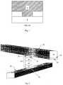
- FIGS. 3 a - 3 care cross-sectional views illustrating stages of formation of a memory array formed according to a preferred embodiment of the present invention.
- FIG. 4is a cross-sectional view of an exemplary diode that may be present in a memory cell formed according to the present invention.
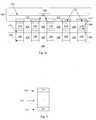
- FIG. 5 ais a perspective view of stacked memory levels with conductors shared between adjacent memory levels according to a preferred embodiment of the present invention.
- FIG. 5 bis a cross-sectional view of several stacked memory levels of such an array.
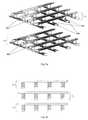
- FIG. 6 ais a perspective view of stacked memory levels with conductors not shared between adjacent memory levels according to a preferred embodiment of the present invention.
- FIG. 6 bis a cross-sectional view of several stacked memory levels of such an array.
- FIG. 7 ais a perspective view of stacked memory levels with conductors shared between some adjacent memory levels and not shared between other adjacent memory levels according to a preferred embodiment of the present invention.
- FIG. 7 bis a cross-sectional view of such an array.
- FIG. 8is a perspective view of a memory cell according to an embodiment of the present invention in which the cell does not include an isolation device.
- FIGS. 9 a and 9 bare cross-sectional views showing formation of memory cells and a contact according to an embodiment of the present invention in which the cell does not include an isolation device.
- phase change materialwill be used to describe a material that changes relatively easily from one stable state to another.
- the phase changeis typically from an amorphous state to a crystalline state (or vice versa), but may be an intermediate change, such as from a less-ordered to a more ordered crystalline state, or vice versa.
- Chalcogenidesare well-known phase change materials.
- phase change materialssuch as chalcogenides
- a nonvolatile memory cellin which a high-resistance, amorphous state represents one memory state while a low-resistance, crystalline state represents the other memory state, where memory states correspond to a value of 1 or 0.
- Chalcogenidesare particularly useful examples of phase change materials, but it will be understood that other materials which undergo reliably detectable stable phase changes, such as silicon, can be used instead.
- Phase change materialis converted from one state to the other by heating to high temperature.
- mechanismshave been used to concentrate heat in a relatively small area contacting the phase change material.
- the phase change material 6is formed with a portion having a narrow cross-section contacting a heater element 8 .
- the achievable reduction in areais dictated by the limits of photolithography; ie the contact can be no smaller than the minimum feature size that can be patterned and etched.
- the present inventiontakes a different approach, providing a simple, easily manufacturable solution to the problem of focusing thermal energy in a non-volatile memory cell comprising a phase change element.
- a nonvolatile memory cellincludes a dielectric layer in series with the phase change material.
- a voltageis applied across the dielectric layer sufficient to cause dielectric breakdown across the dielectric layer, creating a low-resistance rupture region (or, in some cases, possibly more than one.)
- the diameter of such a rupture regionis very small.
- a typical rupture region formed by applying a voltage across a silicon dioxide layer about 10 to about 20 angstroms thick sufficient to cause dielectric breakdown, for example,may be about 50 to about 100 angstroms in diameter.
- Such a dielectric layer in which a low-resistance rupture region is formedis an example of an antifuse.
- An antifuseis characterized by the property of being insulating as formed, preventing current flow; then, when exposed to a high voltage, irreversibly changing its character to become conductive (at least in some regions) and allowing the flow of current.
- the very narrow rupture regionserves to focus the thermal energy into an extremely small volume, aiding conversion of phase change material in series with the dielectric layer having the rupture region.
- the dielectric layer having the rupture region and the phase change materialmay be formed in series, interposed between conductors.
- Other elementsmay exist in the cell, such as a heater layer and a diode.
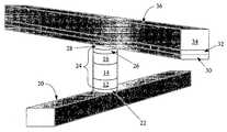
- FIG. 2An exemplary nonvolatile memory cell formed according to the present invention is shown in FIG. 2 . It will be understood that this cell is just one example of the many forms a nonvolatile memory cell according to the present invention might take.
- Bottom conductor 20is formed of a conductive material, for example a refractory metal or refractory metal compound such as tungsten or titanium tungsten.
- bottom conductor 20is in the form of a rail.
- a barrier layer 22 of, for example, titanium nitridemay be used between conductor 20 and polysilicon diode 24 .
- Polysilicon diode 24may comprise a bottom heavily doped layer 12 of a first conductivity type, a middle lightly doped or intrinsic layer 14 , and a top heavily doped layer 16 of a second conductivity type opposite the first conductivity type.
- a thin low thermal conductivity layer 26is formed on the diode.
- Heater layer 26can be formed of, for example, cobalt silicide.
- a layer 28 of dielectric material, for example silicon dioxide,is formed on heater layer 26 .
- titanium nitride layer 22 , diode 24 , heater layer 26 and silicon dioxide layer 28are in the form of a vertically oriented pillar.
- a layer 30 of phase change materialin this example a chalcogenide, is formed above silicon dioxide layer 28 .
- chalcogenide layer 30is a layer of a conductive material 34 , for example a refractory metal or refractory metal compound such as tungsten or titanium tungsten.
- a barrier layer 32 of titanium nitridemay be disposed between the chalcogenide layer 30 and conductive layer 34 .
- chalcogenide layer 30 , barrier layer 32 , and conductive layer 34are in the form of a rail-shaped top conductor 36 .
- Top conductor 36is preferably perpendicular to bottom conductor 20 .
- silicon dioxide layer 28When this memory cell is initially formed, silicon dioxide layer 28 is intact. After a voltage sufficient to cause dielectric breakdown is applied between bottom conductor 20 and top conductor 36 , a low resistance rupture region (not shown) forms traversing silicon dioxide layer 28 from heater layer 26 to chalcogenide layer 30 . This low resistance rupture region is a permanent feature. After its formation, when voltage is applied between conductors 20 and 36 , this rupture region provides a low-resistance current path through silicon dioxide layer 28 .
- the memory cell just describedincludes a non-ohmic conductive element, the diode 24 , to serve as an isolation device.
- a non-ohmic conductive elementis characterized by a non-linear current vs. voltage curve.
- Other non-ohmic elementsmay be used in place of the diode.
- a metal-insulator-metal deviceconsists of two metal (or metal-like) layers separated by a very thin insulator layer. When sufficient voltage is applied, charge carriers can tunnel across the insulator layer, but do not permanently damage it, as in an antifuse.
- the diode 24 of the memory cell of FIG. 2could be replaced with a MIM device.
- suitable materialscan be used for any of the elements of the cell just described.
- titanium nitride replacecan cobalt silicide in heater layer 26 .
- suitable materials for heater layer 26would be any conductor having sheet resistance preferably between about 100 kiloOhm/ ⁇ and about 1 kiloOhm/ ⁇ .
- Other metal silicidescan be used, for example, or refractory metal compounds.
- a detailed examplewill be provided describing fabrication of a monolithic three dimensional memory array, the nonvolatile memory cells of the array formed according to one preferred embodiment of the present invention.
- the example arraywill include a diode, as in the memory cell just described, though other configurations could be used instead; for example some other non-ohmic conductive element, such as a MIM, could be substituted for the diode.
- a MIMnon-ohmic conductive element
- This substrate 100can be any semiconducting substrate as known in the art, such as monocrystalline silicon, IV-IV compounds like silicon-germanium or silicon-germanium-carbon, III-V compounds, II-VII compounds, epitaxial layers over such substrates, or any other semiconducting material.
- the substratemay include integrated circuits fabricated therein.
- the insulating layer 102is formed over substrate 100 .
- the insulating layer 102can be silicon oxide, silicon nitride, high-dielectric film, Si—C—O—H film, or any other suitable insulating material.
- the first conductors 200are formed over the substrate and insulator.
- An adhesion layer 104may be included between the insulating layer 102 and the conducting layer 106 to help the conducting layer 106 adhere.
- Preferred materials for the adhesion layer 104are tantalum nitride, tungsten nitride, titanium tungsten, tungsten, titanium nitride, or combinations of these materials. If the overlying conducting layer is tungsten, titanium nitride is preferred as adhesion layer 104 .
- Conducting layer 106can comprise any conducting material known in the art, including tantalum, titanium, tungsten, copper, cobalt, or alloys thereof. Titanium nitride may be used.
- the layerswill be patterned and etched using any suitable masking and etching process to form substantially parallel, substantially coplanar conductors 200 , shown in FIG. 3 a in cross-section.
- photoresistis deposited, patterned by photolithography and the layers etched, and then the photoresist removed using standard process techniques.
- Conductors 200could be formed by a Damascene method instead.
- Dielectric material 108is deposited over and between conductor rails 200 .
- Dielectric material 108can be any known electrically insulating material, such as silicon oxide, silicon nitride, or silicon oxynitride. In a preferred embodiment, silicon oxide is used as dielectric material 108 .
- a barrier layer 110is deposited as the first layer after planarization of the conductor rails.
- Any suitable materialcan be used in the barrier layer, including tungsten nitride, tantalum nitride, titanium nitride, or combinations of these materials.
- titanium nitrideis used as the barrier layer.
- the barrier layeris titanium nitride, it can be deposited in the same manner as the adhesion layer described earlier.
- the semiconductor materialcan be silicon, silicon-germanium, silicon-germanium-carbon, germanium, or other suitable semiconductors or compounds.
- One of the most commonly used chalcogenide materialsis Ge 2 Sb 2 Te 5 , which has a melting temperature of 610 degrees C.
- Germanium and silicon-germanium alloyscrystallize at lower temperatures than silicon, and may be useful in reducing the temperatures required to fabricate the structure to be described. For simplicity, this description will refer to the semiconductor material as silicon, but it will be understood that the skilled practitioner may select any of these other suitable materials instead.
- the pillarcomprises a semiconductor junction diode.
- a preferred junction diodehas a bottom heavily doped region 112 , intrinsic region 114 , and top heavily doped region 116 .
- the conductivity type of bottom region 112 and top region 116are opposite: Either region 112 is p-type while region 116 is n-type, or region 112 is n-type while region 116 is p-type.
- Middle region 114is intrinsic, or not intentionally doped, though in some embodiments it may be lightly doped. An undoped region will never be perfectly electrically neutral, and will always have defects or contaminants that cause it to behave as if slightly n-doped or p-doped. Such a diode can be considered a p-i-n diode.
- bottom region 112will be n-type while top region 116 is p-type. It will understood that these conductivity types could be reversed.
- bottom heavily doped region 112can be formed by any deposition and doping method known in the art. The silicon can be deposited and then doped, but is preferably doped in situ by flowing a donor gas providing n-type dopant atoms, for example phosphorus, during deposition of the silicon.
- the next layer 114will be intrinsic undoped silicon.
- This layercan formed by any deposition method known in the art.
- the thickness of the intrinsic silicon layercan range from about 1000 to about 4000 angstroms, preferably about 2500 angstroms.
- siliconis deposited without intentional doping, yet has defects which render it slightly n-type.
- a layer 116 of heavily doped p-type siliconis preferably deposited undoped, and will be doped by ion implantation in a later step.
- the thickness of heavily doped p-type silicon region 116can range from about 100 to about 2000 angstroms, preferably about 800 angstroms. Note this is the thickness as-deposited. Some portion of the top of this layer will be consumed in a subsequent CMP or etchback step, and will thus be thinner in the finished device.
- Pillars 300should have about the same pitch and about the same width as conductors 200 below, such that each pillar 300 is formed on top of a conductor 200 . Some misalignment can be tolerated.
- the diodesare formed by depositing a semiconductor layer stack and patterning and etching the layer stack to form a pillar.
- the pillars 300can be formed using any suitable masking and etching process.
- photoresistcan be deposited, patterned using standard photolithography techniques, and etched, then the photoresist removed.
- a hard mask of some other materialfor example silicon dioxide, can be formed on top of the semiconductor layer stack, with bottom antireflective coating (BARC) on top, then patterned and etched.
- BARCbottom antireflective coating
- DARCdielectric antireflective coating
- Dielectric material 108is deposited over and between the semiconductor pillars 300 , filling the gaps between them.
- Dielectric material 108can be any known electrically insulating material, such as silicon oxide, silicon nitride, or silicon oxynitride. In a preferred embodiment, silicon dioxide is used as the insulating material.
- the dielectric material on top of the pillars 300is removed, exposing the tops of pillars 300 separated by dielectric material 108 , and leaving a substantially planar surface.
- This removal of dielectric overfillcan be performed by any process known in the art, such as CMP or etchback.
- CMP or etchbackion implantation is performed, heavily doping top region 116 of the diode with a p-type dopant, for example boron.
- a p-type dopantfor example boron.
- a thin layer of about 20 to about 100 angstroms of cobalt(not shown) is deposited on the dielectric 108 and exposed pillars 300 .
- Cobaltcan be deposited by any conventional method, for example by sputtering.
- Other metals that form metal silicidescan be used in place of cobalt, including chromium, nickel, platinum, niobium, palladium, tantalum, or titanium. For simplicity, this description will detail the use of cobalt, but it will be understood that any of these other metals can be substituted as appropriate.
- the titanium or titanium nitride capassists in the subsequent conversion of the cobalt layer to cobalt silicide.
- an annealis performed at a suitable temperature to react the cobalt with the polysilicon of the exposed diodes to form cobalt silicide 118 on the diodes only; no silicide is formed where the cobalt overlies oxide fill 108 .
- the annealmay be performed in a rapid thermal annealing system at about 400 to about 700 degrees C. for about 20 to about 100 seconds, preferably at about 500 degrees C. for about 30 seconds.
- the capping layer and unreacted portions of the cobaltare removed by a selective etch. Any etching medium which selectively etches the capping layer and the unreacted cobalt while leaving cobalt silicide may be used. Preferably, selective wet etching is used.
- a second annealmay be performed to homogenize the cobalt silicide 118 to CoSi 2 .
- This second annealcan be performed at any time after the first. In a multi-level memory array, preferably a single anneal is performed after all of the memory levels are constructed to homogenize the cobalt silicide. Alternatively, the second anneal can be combined with antifuse growth.
- Layer 118will serve as a heater layer, heating a portion of a phase change layer (still to be formed) to cause it to undergo a desired phase change.
- dielectric layer 120which is preferably an oxide, nitride, or oxynitride layer, is formed on cobalt suicide 118 .
- silicon oxideis grown by exposing the silicide layer 118 to an oxygen atmosphere in a rapid thermal annealing system, preferably at about 670 to about 750 degrees C. for about 20 to about 60 seconds. Note that some but not all of the top heavily doped region 116 has been consumed by the silicide reaction.
- dielectric layer 120could have been deposited instead, or chemically grown. Other materials could be used, for example aluminum oxide. Some of these other methods lend the advantage of lower temperature processing.
- a layer about 20 angstroms thickmay be deposited by DC-magnetron sputtering in a vacuum system and plasma oxidizing in an O 2 atmosphere at 100 mTorr for two to six minutes.
- the resistance of the resulting aluminum oxide layeris about 10 megaOhms/micron 2 .
- such a layercould be formed by any other conventional method.
- Next layer 122 of a phase change materialis formed on dielectric layers 120 and intervening dielectric material 108 .
- Layer 122can be any chalcogenide material, for example any suitable compound of germanium (Ge), antimony (Sb) and tellurium (Te); such a compound is referred to as a GST material.
- Phase change layer 122can be formed by any conventional method.
- a thin barrier layer 124is formed on phase change layer 122 .
- Barrier layer 124provides a barrier between phase change layer 122 and conductive layer 126 .
- Conductive layer 126is formed of a conductive material, for example tungsten.
- Phase change material layer 122 , barrier layer 124 , and conductive layer 126are then patterned and etched using any suitable masking and etching process to form substantially parallel, substantially coplanar conductors 400 , shown in FIG. 3 c extending left-to-right across the page.
- photoresistis deposited, patterned by photolithography and the layers etched, and then the photoresist removed using standard process techniques.
- the dielectric materialcan be any known electrically insulating material, such as silicon oxide, silicon nitride, or silicon oxynitride. In a preferred embodiment, silicon oxide is used as this dielectric material.
- Each memory cell just createdis a nonvolatile memory cell comprising a bottom conductor; a top conductor; a dielectric layer having a low-resistance ruptured region therethrough; and a layer of phase change material, wherein the layer of phase change material is in thermal contact with the dielectric layer, wherein the dielectric layer and the layer of phase change material are disposed between the bottom conductor and the top conductor, and wherein the dielectric layer and the layer of phase change material are part of the memory cell.
- a layer or elementis considered to be in thermal contact with phase change material when thermal events within that layer or element are capable of thermally affecting the phase change material sufficient to cause it to detectably change phase.
- nonvolatile memory arraycomprising a plurality of substantially parallel, substantially coplanar first conductors formed at a first height above a substrate; a plurality of substantially parallel, substantially coplanar second conductors formed at a second height, the second height above the first height; a plurality of first phase change elements disposed between the first and second conductors; a plurality of first dielectric layers, each first dielectric layer in thermal contact with one of the plurality of first phase change elements, each of the first dielectric layers having a high-conductance ruptured region therethrough; and a plurality of first memory cells, wherein each memory cell of the plurality comprises a) one of the first phase change elements, b) one of the first dielectric layers, c) a portion of one of the first conductors, and d) a portion of one of the second conductors.
- This structureis a first memory level. Additional memory levels can be monolithically formed above this memory level to form a monolithic three dimensional memory array.
- a monolithic three dimensional memory arrayis one in which multiple memory levels are formed above a single substrate, such as a wafer, with no intervening substrates.
- stacked memorieshave been constructed by forming memory levels on separate substrates and adhering the memory levels atop each other, as in Leedy, U.S. Pat. No. 5,915,167, “Three dimensional structure memory.” The substrates may be thinned or removed from the memory levels before bonding, but as the memory levels are initially formed over separate substrates, such memories are not true monolithic three dimensional memory arrays.
- a second memory levelcan be formed above the first memory level just described.
- top conductors 400can be shared between adjacent memory levels. Turning to FIG. 5 a , if top conductors 400 are to be shared, after planarization second pillars 500 are formed in the same manner as were the first pillars 300 , each on one of the conductors 400 .
- a third plurality of substantially parallel, substantially coplanar conductors 600preferably substantially perpendicular to second conductors 400 , are formed above second pillars 500 . It will be seen that conductors 400 belong to both memory level L 0 and to memory level L 1 .
- the p-i-n diodes in the second pillars 500may be upside down relative to the p-i-n diodes of first pillars 300 ; eg if, in first pillars 300 , the bottom heavily doped region is n-type and the top heavily doped region is p-type, then in second pillars 500 the bottom heavily doped region may be p-type while the top heavily doped region is n-type.
- FIG. 5 bshows five memory levels in cross section, illustrating how this scheme can be extended for several stacked levels.
- One plurality of conductorsis shared between L 0 and L 1 , a different plurality of conductors is shared between L 1 and L 2 , etc.
- an interlevel dielectric(not shown) can be formed between adjacent memory levels.
- third conductors 600are formed above the interlevel dielectric, second pillars 500 formed above third conductors 600 , and fourth conductors 700 formed above second pillars 500 .
- Conductors 400belong to memory level L 0 only, while conductors 600 and 700 belong to memory level L 1 .
- No conductorsare shared between memory levels.
- FIG. 6 bshows a cross-sectional view of an array in which this scheme is extended for three memory levels. No conductors are shared between memory levels L 0 and L 1 , or between memory levels L 1 and L 2 . If desired, adjacent memory levels sharing conductors and adjacent memory levels not sharing conductors can be stacked in the same monolithic three dimensional memory array.
- FIG. 7 ashows a memory array in which conductors 400 are shared between memory levels L 0 and L 1 , and conductors 600 are shared between memory levels L 2 and L 3 . No conductors are shared between memory levels L 1 and L 2 , however.
- FIG. 7 bshows a cross-sectional view of such an array. Other configurations can be envisioned, and fall within the scope of the present invention.
- Memory levelsneed not all be formed having the same style of memory cell. If desired, memory levels using phase change materials can alternate with memory levels using other types of memory cells.
- the various monolithic three dimensional memory arrays describedcomprise a) a first memory level, the first memory level comprising: i) a plurality of substantially coplanar first conductors; ii) a plurality of substantially coplanar second conductors above the first conductors; iii) a plurality of first dielectric regions, each having a low-resistance ruptured region therethrough; iv) a plurality of first phase change elements, each phase change element in series with the ruptured region of one of the first dielectric regions, wherein each of the first dielectric regions and each of the first phase change elements are disposed between one of the first conductors and one of the second conductors; and b) a second memory level monolithically formed above the first memory level.
- the chalcogenideTo convert a chalcogenide in a crystalline, low-resistance state to an amorphous, high-resistance state, the chalcogenide must be brought to a high temperature, for example about 700 degrees C., then allowed to cool quickly.
- the reverse conversion from an amorphous, high-resistance state to a crystalline, low-resistance stateis achieved by heating to a lower temperature, for example about 600 degrees C., then allowing the chalcogenide to cool relatively slowly.
- Circuit conditionsmust be carefully controlled in a monolithic three dimensional memory array formed according to the present invention to avoid inadvertent conversion of the chalcogenide of neighboring cells during programming of a cell, or during repeated read events.
- Circuit structures and methods suitable for use in three dimensional memory arrays formed according to the present inventionare described in Scheuerlein, U.S. patent application Ser. No. 10/403,844, “Word Line Arrangement Having Multi-Layer Word Line Segments for Three-Dimensional Memory Array,” filed Mar. 31, 2003, which is assigned to the assignee of the present invention and is hereby incorporated by reference.
- Beneficial elements of this arrangementinclude use of a common word line driver and very long bitlines allowing reduction in overhead circuitry.
- the resistance of the programmed cell during programmingshould be about the same as the sum of the resistance of the circuits driving the wordline and bitline of the selected cell.
- the dielectric regionWhen a low-resistance rupture region is electrically formed by dielectric breakdown across the dielectric layer, the dielectric region is originally high resistance, then drops in resistance as the rupture region forms. As the resistance of the rupture region approaches that of the circuit, the rupture region begins to cool, and will not further increase in size. Thus the formation mechanism of the rupture region tends to cause the rupture region to have about the same resistance as the resistance of the driving circuit. In subsequent programming events, then, the rupture region provides a means to deliver predictable levels of power to the cell.
- Conventional current limiter circuitrymay advantageously be used to control the effective resistance of drivers during programming, as will be well understood by those skilled in the art.
- the initial resistance of the unruptured antifusewill be very high, between about 1 megaOhm and about 1000 megaOhms. After dielectric breakdown, the resistance of the rupture region will be between about 1 and about 100 kiloOhms.
- the resistance of the chalcogenide materialwhen in the high-resistance state, will range from about 50 kiloOhms to about 2 megaOhms. In the low-resistance state, resistance drops to between about 1 kiloOhm to about 100 kiloOhms; in the example given, resistance is preferably about 3 kiloOhms.
- the heater layersimilarly has resistance ranging from about 1 kiloOhm to about 100 kiloOhms, in the example given preferably about 2 kiloOhms.
- the resistances of the heater layerabout 2 kiloOhms
- the rupture region of the dielectricabout 1 kiloOhm
- the chalcogenide materialabout 1 kiloOhm
- the resistance of the cellis about 5 kiloOhms, and the power that can be delivered to the cell by providing low resistance driving circuitry is high enough to reach temperatures sufficient to cause phase conversion, even with short pulses. Subsequently the cell is in the high-resistance state, and the maximum power that can be delivered to the circuit is much lower.
- the driving circuitryis capable of delivering a voltage to the cell above a characteristic threshold voltage in the range of one to two volts which causes current to flow through the high-resistance cell. The power delivered to the cell is limited by the driving circuitry to a level desired for setting the cell in its low-resistance state.
- a most preferred mode of operating memory cells formed according to the present inventionwould be to form the memory as described herein, then to form the low-resistance rupture region in the dielectric layer of every cell under controlled conditions as a preconditioning step before the device is delivered to the end user.
- the rupture eventleaves the memory cell in the high-resistance state.
- the cellsare all converted to the crystalline, low-resistance state, final testing of the device is performed, and the memory is ready for use.
- the memorycan be delivered to the end user with the dielectric antifuses intact, and the rupture event could double as a programming event.
- the initial state of cellscould be either low-resistance or high-resistance.
- a method for forming and programming a nonvolatile memory cellcomprising forming a layer of phase change material; forming a dielectric layer in thermal contact with the layer of phase change material; and forming a low-resistance rupture region through the dielectric layer.
- the cellcan then be programmed wherein, during programming, a programming current flows through the low-resistance rupture region. Programming the cell changes it from the first state (low- or high-resistance) to a second state (high- or low-resistance). The cell can subsequently be “erased”, returning it to the first state.
- diode 24can be replaced with a MIM or with some other non-ohmic conductive element.
- the diodeAfter the rupture region is formed in a cell, the diode is in electrical contact with the phase change material, though it may not be in physical contact. One layer is in electrical contact with another when no dielectric layer sufficient to impede current flow is disposed between them.
- phase change layerneed not appear in precisely the same orientation or order shown in FIG. 2 .
- the dielectric layercould be below the diode rather than above, for example, as could the phase change material.
- the phase change layer 30 and the heater layer 26are on opposite sides of dielectric layer 28 .
- Such a cellcan be formed by a method comprising forming a layer of phase change material; forming a heater layer; forming a dielectric layer disposed between the layer of phase change material and the heater layer and in contact with both; and forming a low-resistance rupture region through the dielectric layer.
- the memory cell of FIG. 2for example, comprises a bottom conductor; a top conductor; a dielectric layer having a low-resistance ruptured region therethrough; a layer of phase change material; and a heater layer; wherein the dielectric layer is disposed between and in contact with the layer of phase change material and the heater layer, and wherein the dielectric layer and the layer of phase change material are disposed between the bottom conductor and the top conductor, and wherein the dielectric layer and the layer of phase change material are part of the memory cell.
- the dielectric layer, heater layer, and phase change layermay be arranged in a different order.
- Bottom rail 20is formed of conductive layer 18 , which comprises a conductive material such as tungsten, and heater layer 26 which is formed of, for example, titanium nitride or any other suitable material as described in other embodiments.
- Dielectric layer 28can be any deposited dielectric, for example aluminum oxide.
- Phase change layer 30is, for example, a chalcogenide, or GST material.
- Above phase change layer 30 in top conductor 36is conductive layer 19 of any suitable conductive material, such as tungsten. Bottom conductor 20 and top conductor 36 are patterned and etched using any conventional method. If desired, the locations of phase change layer 30 and heater layer 26 could be reversed.
- FIGS. 9 a and 9 bFormation of another example of such an array in which memory cells have no isolation device such as a diode or MIM is illustrated in FIGS. 9 a and 9 b .
- the bottom rails 20are formed of a conductive material 19 such as tungsten and a layer 30 of a phase change material, for example a chalcogenide.
- a barrier layer 31may be included.
- a dielectric material 108is deposited over and between bottom rails 20 .
- the surfaceis planarized, for example by CMP. This CMP step does not expose rails 20 , and they remain covered with dielectric material 108 .
- a hole 130is etched through dielectric material 108 in the array at each location where a cell is to be formed.
- Thin dielectric layer 28formed of, for example, a nitride, oxide, or oxynitride, is deposited, filling etched hole 130 . If the deposited dielectric material deposits on sidewalls, it will coat the walls and the bottom of the etched hole, but only coverage at the bottom of the etched hole is important for device performance.
- holes 132are etched for contacts outside of the array, shown in 9 b .
- Photoresistis removed and a heater layer 26 , for example of titanium nitride, is deposited to line both holes 130 in the array and contact holes 132 .
- a conductive materialfor example tungsten fills the holes and forms a conductive layer 134 .
- Conductive layer 134 and heater layer 26are patterned and etched to form top rails 36 , preferably extending perpendicular to bottom rails 20 . It will be seen that dielectric layer 28 separates phase change layer 30 and heater layer 26 only in the memory cells, not in the contacts.
- Monolithic three dimensional memory arraysare described in Johnson et al., U.S. Pat. No. 6,034,882, “Vertically stacked field programmable nonvolatile memory and method of fabrication”; Johnson, U.S. Pat. No. 6,525,953, “Vertically stacked field programmable nonvolatile memory and method of fabrication”; Knall et al., U.S. Pat. No. 6,420,215, “Three Dimensional Memory Array and Method of Fabrication”; and Vyvoda et al., U.S. patent application Ser. No. 10/185,507, “Electrically Isolated Pillars in Active Devices,” filed Jun. 27, 2002; U.S. patent application Ser. No.
- the present inventionhas been described herein in the context of a monolithic three dimensional memory array formed above a substrate.
- Such an arraycomprises at least a first memory level formed at a first height above the substrate and a second memory level formed at a second height different from the first height.
- Three, four, eight, or indeed any number of memory levelscan be formed above the substrate in such a multilevel array.
- a memory array comprising memory cells formed according to the present inventionneed not be formed in a three dimensional array, and could be a more conventional two dimensional array formed without stacking.
Landscapes
- Engineering & Computer Science (AREA)
- Computer Hardware Design (AREA)
- Chemical & Material Sciences (AREA)
- Crystallography & Structural Chemistry (AREA)
- Semiconductor Memories (AREA)
Abstract
Description
- This application is a continuation-in-part of Herner et al., U.S. patent application Ser. No. 10/855,784, “An Improved Method for Making High-Density Nonvolatile Memory,” filed May 26, 2004; which is a continuation of Herner et al., U.S. patent application Ser. No. 10/326,470, “An Improved Method for Making High-Density Nonvolatile Memory,” filed Dec. 19, 2002 (since abandoned) and hereinafter the '470 application, both assigned to the assignee of the present invention and hereby incorporated by reference in their entirety.
- This application is related to Scheuerlein, U.S. application Ser. No. ______, “Structure and Method for Biasing Phase Change Memory Array for Reliable Writing,” (attorney docket number MA-132); to Scheuerlein, U.S. application Ser. No. ______ “A Non-Volatile Phase Change Memory Cell Having a Reduced Thermal Contact Area,” (attorney docket number MA-133); and to Scheuerlein, U.S. application Ser. No. ______, “A Write-Once Nonvolatile Phase Change Memory Array,” (attorney docket number MA-134); all filed on even date herewith and hereby incorporated by reference.
- The invention relates to a nonvolatile memory cell comprising a dielectric layer and a phase-change element in series.
- Phase-change materials such as chalcogenides have been used in nonvolatile memories. Such materials can exist in one of two or more stable states, for example a high-resistance and a low-resistance state. In chalcogenides, the high-resistance state corresponds to an amorphous state, while the low-resistance state corresponds to a more ordered crystalline state. The conversion between states is generally achieved thermally.
- Conversion from one phase to another is achieved most effectively if the thermal energy is focused into a relatively small area. Some prior art devices have tried to focus thermal energy by forming a very small contact area using photolithography. The limits of photolithography, however, restrict the usefulness of this approach. A need exists, therefore, for a method to concentrate heat in a phase change memory in a volume smaller than that easily achievable using photolithography.
- The present invention is defined by the following claims, and nothing in this section should be taken as a limitation on those claims. In general, the invention is directed to a nonvolatile memory cell comprising a phase change element and a dielectric layer in series.
- A first aspect of the invention provides for a method for forming and programming a nonvolatile memory cell, the method comprising forming a layer of phase change material; forming a dielectric layer in thermal contact with the layer of phase change material; and forming a low-resistance rupture region through the dielectric layer.
- Another aspect of the invention provides for a nonvolatile memory cell comprising: a bottom conductor; a top conductor; a dielectric layer having a low-resistance ruptured region therethrough; and a layer of phase change material, wherein the layer of phase change material is in thermal contact with the dielectric layer, wherein the dielectric layer and the layer of phase change material are disposed between the bottom conductor and the top conductor, and wherein the dielectric layer and the layer of phase change material are part of the memory cell.
- A preferred embodiment of the invention provides for a nonvolatile memory array comprising a plurality of substantially parallel, substantially coplanar first conductors formed at a first height above a substrate; a plurality of substantially parallel, substantially coplanar second conductors formed at a second height, the second height above the first height; a plurality of first phase change elements disposed between the first and second conductors; a plurality of first dielectric layers, each first dielectric layer in thermal contact with one of the plurality of first phase change elements, each of the first dielectric layers having a high-conductance ruptured region therethrough; and a plurality of first memory cells, wherein each memory cell of the plurality comprises a) one of the first phase change elements, b) one of the first dielectric layers, c) a portion of one of the first conductors, and d) a portion of one of the second conductors.
- Another aspect of the invention provides for a monolithic three dimensional memory array comprising: a) a first memory level, the first memory level comprising: i) a plurality of substantially coplanar first conductors; ii) a plurality of substantially coplanar second conductors above the first conductors; iii) a plurality of first dielectric regions, each having a low-resistance ruptured region therethrough; iv) a plurality of first phase change elements, each phase change element in series with the ruptured region of one of the first dielectric regions, wherein each of the first dielectric regions and each of the first phase change elements are disposed between one of the first conductors and one of the second conductors; and b) a second memory level monolithically formed above the first memory level.
- Another preferred embodiment of the invention provides for a method for forming and programming a plurality of memory cells, the method comprising: forming a plurality of substantially coplanar first conductors above a substrate; forming a plurality of substantially coplanar second conductors above the first conductors; forming a plurality of first dielectric regions; forming a plurality of first phase change elements, each in thermal contact with one of the first dielectric regions, wherein each of the first phase change elements and each of first dielectric regions are disposed between one of the first conductors and one of the second conductors; forming a low-resistance ruptured region through each of the first dielectric regions; and causing a phase change of any of the phase change elements by flowing a current through the low-resistance ruptured region of one of the first dielectric regions.
- Yet another aspect of the invention provides for a method for forming and programming a nonvolatile memory cell, the method comprising: forming a layer of phase change material; forming a heater layer; forming a dielectric layer disposed between the layer of phase change material and the heater layer and in contact with both; and forming a low-resistance rupture region through the dielectric layer.
- A related aspect of the invention provides for a nonvolatile memory cell comprising: a bottom conductor; a top conductor; a dielectric layer having a low-resistance ruptured region therethrough; a layer of phase change material; and a heater layer; wherein the dielectric layer is disposed between and in contact with the layer of phase change material and the heater layer, and wherein the dielectric layer and the layer of phase change material are disposed between the bottom conductor and the top conductor, and wherein the dielectric layer and the layer of phase change material are part of the memory cell.
- Each of the aspects and embodiments of the invention described herein can be used alone or in combination with one another.
- The preferred aspects and embodiments will now be described with reference to the attached drawings.
FIG. 1 is a cross-sectional view of a portion of a prior art memory cell.FIG. 2 is a perspective view of a nonvolatile memory cell formed according to an embodiment of the present invention.FIGS. 3 a-3care cross-sectional views illustrating stages of formation of a memory array formed according to a preferred embodiment of the present invention.FIG. 4 is a cross-sectional view of an exemplary diode that may be present in a memory cell formed according to the present invention.FIG. 5 ais a perspective view of stacked memory levels with conductors shared between adjacent memory levels according to a preferred embodiment of the present invention.FIG. 5 bis a cross-sectional view of several stacked memory levels of such an array.FIG. 6 ais a perspective view of stacked memory levels with conductors not shared between adjacent memory levels according to a preferred embodiment of the present invention.FIG. 6 bis a cross-sectional view of several stacked memory levels of such an array.FIG. 7 ais a perspective view of stacked memory levels with conductors shared between some adjacent memory levels and not shared between other adjacent memory levels according to a preferred embodiment of the present invention.FIG. 7 bis a cross-sectional view of such an array.FIG. 8 is a perspective view of a memory cell according to an embodiment of the present invention in which the cell does not include an isolation device.FIGS. 9 aand9bare cross-sectional views showing formation of memory cells and a contact according to an embodiment of the present invention in which the cell does not include an isolation device.- While all materials can change phase, in this discussion the term “phase change material” will be used to describe a material that changes relatively easily from one stable state to another. The phase change is typically from an amorphous state to a crystalline state (or vice versa), but may be an intermediate change, such as from a less-ordered to a more ordered crystalline state, or vice versa. Chalcogenides are well-known phase change materials.
- It is known to use phase change materials, such as chalcogenides, in a nonvolatile memory cell, in which a high-resistance, amorphous state represents one memory state while a low-resistance, crystalline state represents the other memory state, where memory states correspond to a value of 1 or 0. (If intermediate stable states are achieved, more than two memory states can exist for each cell; for simplicity, the examples in this discussion will describe only two memory states.) Chalcogenides are particularly useful examples of phase change materials, but it will be understood that other materials which undergo reliably detectable stable phase changes, such as silicon, can be used instead.
- Phase change material is converted from one state to the other by heating to high temperature. To facilitate this conversion, mechanisms have been used to concentrate heat in a relatively small area contacting the phase change material. For example, as shown in
FIG. 1 , in some prior art devices, thephase change material 6 is formed with a portion having a narrow cross-section contacting aheater element 8. In such a scheme, the achievable reduction in area is dictated by the limits of photolithography; ie the contact can be no smaller than the minimum feature size that can be patterned and etched. - Another approach to this problem appears in Czubatyj et al., U.S. Pat. No. 5,825,046, “Composite memory material comprising a mixture of phase-change memory material and dielectric material,” in which the phase change material is layered or otherwise mixed with dielectric material to form a composite, thus reducing the volume of actual phase change material present.
- The present invention takes a different approach, providing a simple, easily manufacturable solution to the problem of focusing thermal energy in a non-volatile memory cell comprising a phase change element.
- In aspects of the present invention, a nonvolatile memory cell includes a dielectric layer in series with the phase change material. A voltage is applied across the dielectric layer sufficient to cause dielectric breakdown across the dielectric layer, creating a low-resistance rupture region (or, in some cases, possibly more than one.) The diameter of such a rupture region is very small. A typical rupture region formed by applying a voltage across a silicon dioxide layer about 10 to about 20 angstroms thick sufficient to cause dielectric breakdown, for example, may be about 50 to about 100 angstroms in diameter.
- Such a dielectric layer in which a low-resistance rupture region is formed is an example of an antifuse. An antifuse is characterized by the property of being insulating as formed, preventing current flow; then, when exposed to a high voltage, irreversibly changing its character to become conductive (at least in some regions) and allowing the flow of current.
- The very narrow rupture region serves to focus the thermal energy into an extremely small volume, aiding conversion of phase change material in series with the dielectric layer having the rupture region. For example, the dielectric layer having the rupture region and the phase change material may be formed in series, interposed between conductors. Other elements may exist in the cell, such as a heater layer and a diode.
- An exemplary nonvolatile memory cell formed according to the present invention is shown in
FIG. 2 . It will be understood that this cell is just one example of the many forms a nonvolatile memory cell according to the present invention might take. Bottom conductor 20 is formed of a conductive material, for example a refractory metal or refractory metal compound such as tungsten or titanium tungsten. In this exemplary cell,bottom conductor 20 is in the form of a rail. Abarrier layer 22 of, for example, titanium nitride may be used betweenconductor 20 andpolysilicon diode 24. (In this discussion, the term “polysilicon” will be used to describe polycrystalline silicon.)Polysilicon diode 24 may comprise a bottom heavily dopedlayer 12 of a first conductivity type, a middle lightly doped orintrinsic layer 14, and a top heavily dopedlayer 16 of a second conductivity type opposite the first conductivity type. A thin lowthermal conductivity layer 26 is formed on the diode. This layer acts as a heater.Heater layer 26 can be formed of, for example, cobalt silicide. Alayer 28 of dielectric material, for example silicon dioxide, is formed onheater layer 26. In the embodiment shown inFIG. 2 ,titanium nitride layer 22,diode 24,heater layer 26 andsilicon dioxide layer 28 are in the form of a vertically oriented pillar.- A
layer 30 of phase change material, in this example a chalcogenide, is formed abovesilicon dioxide layer 28. Abovechalcogenide layer 30 is a layer of aconductive material 34, for example a refractory metal or refractory metal compound such as tungsten or titanium tungsten. Abarrier layer 32 of titanium nitride may be disposed between thechalcogenide layer 30 andconductive layer 34. In this embodiment,chalcogenide layer 30,barrier layer 32, andconductive layer 34 are in the form of a rail-shapedtop conductor 36.Top conductor 36 is preferably perpendicular tobottom conductor 20. - When this memory cell is initially formed,
silicon dioxide layer 28 is intact. After a voltage sufficient to cause dielectric breakdown is applied betweenbottom conductor 20 andtop conductor 36, a low resistance rupture region (not shown) forms traversingsilicon dioxide layer 28 fromheater layer 26 to chalcogenidelayer 30. This low resistance rupture region is a permanent feature. After its formation, when voltage is applied betweenconductors silicon dioxide layer 28. - The cell just described is just one example of the forms that a nonvolatile memory cell formed according to the present invention may take; clearly many other configurations are possible. For example, the memory cell just described includes a non-ohmic conductive element, the
diode 24, to serve as an isolation device. A non-ohmic conductive element is characterized by a non-linear current vs. voltage curve. Other non-ohmic elements may be used in place of the diode. For example, a metal-insulator-metal device consists of two metal (or metal-like) layers separated by a very thin insulator layer. When sufficient voltage is applied, charge carriers can tunnel across the insulator layer, but do not permanently damage it, as in an antifuse. In alternative embodiments of the present invention, thediode 24 of the memory cell ofFIG. 2 could be replaced with a MIM device. - Other suitable materials can be used for any of the elements of the cell just described. For example, titanium nitride replace can cobalt silicide in
heater layer 26. Other suitable materials forheater layer 26 would be any conductor having sheet resistance preferably between about 100 kiloOhm/□ and about 1 kiloOhm/□. Other metal silicides can be used, for example, or refractory metal compounds. - A detailed example will be provided describing fabrication of a monolithic three dimensional memory array, the nonvolatile memory cells of the array formed according to one preferred embodiment of the present invention. The example array will include a diode, as in the memory cell just described, though other configurations could be used instead; for example some other non-ohmic conductive element, such as a MIM, could be substituted for the diode. For completeness, specific process conditions, dimensions, methods, and materials will be provided. It will be understood, however, that such details are not intended to be limiting, and that many of these details can be modified, omitted or augmented while the results still fall within the scope of the invention.
- Fabrication
- Fabrication of a single memory level will be described in detail. Additional memory levels can be stacked, each monolithically formed above the one below it.
- Turning to
FIG. 3 a, formation of the memory begins with asubstrate 100. Thissubstrate 100 can be any semiconducting substrate as known in the art, such as monocrystalline silicon, IV-IV compounds like silicon-germanium or silicon-germanium-carbon, III-V compounds, II-VII compounds, epitaxial layers over such substrates, or any other semiconducting material. The substrate may include integrated circuits fabricated therein. - An insulating
layer 102 is formed oversubstrate 100. The insulatinglayer 102 can be silicon oxide, silicon nitride, high-dielectric film, Si—C—O—H film, or any other suitable insulating material. - The
first conductors 200 are formed over the substrate and insulator. Anadhesion layer 104 may be included between the insulatinglayer 102 and theconducting layer 106 to help theconducting layer 106 adhere. Preferred materials for theadhesion layer 104 are tantalum nitride, tungsten nitride, titanium tungsten, tungsten, titanium nitride, or combinations of these materials. If the overlying conducting layer is tungsten, titanium nitride is preferred asadhesion layer 104. - The next layer to be deposited is conducting
layer 106. Conductinglayer 106 can comprise any conducting material known in the art, including tantalum, titanium, tungsten, copper, cobalt, or alloys thereof. Titanium nitride may be used. - Once all the layers that will form the conductor rails have been deposited, the layers will be patterned and etched using any suitable masking and etching process to form substantially parallel, substantially
coplanar conductors 200, shown inFIG. 3 ain cross-section. In one embodiment, photoresist is deposited, patterned by photolithography and the layers etched, and then the photoresist removed using standard process techniques.Conductors 200 could be formed by a Damascene method instead. - Next a
dielectric material 108 is deposited over and between conductor rails200.Dielectric material 108 can be any known electrically insulating material, such as silicon oxide, silicon nitride, or silicon oxynitride. In a preferred embodiment, silicon oxide is used asdielectric material 108. - Finally, excess
dielectric material 108 on top ofconductor rails 200 is removed, exposing the tops ofconductor rails 200 separated bydielectric material 108, and leaving a substantiallyplanar surface 109. The resulting structure is shown inFIG. 3 a. This removal of dielectric overfill to formplanar surface 109 can be performed by any process known in the art, such as chemical mechanical planarization (CMP) or etchback. At this stage, a plurality of substantially parallel first conductors have been formed at a first height abovesubstrate 100. - Next, turning to
FIG. 3 b, vertical pillars will be formed above completed conductor rails200. (To savespace substrate 100 is not shown inFIG. 3 b; its presence will be assumed.) Preferably abarrier layer 110 is deposited as the first layer after planarization of the conductor rails. Any suitable material can be used in the barrier layer, including tungsten nitride, tantalum nitride, titanium nitride, or combinations of these materials. In a preferred embodiment, titanium nitride is used as the barrier layer. Where the barrier layer is titanium nitride, it can be deposited in the same manner as the adhesion layer described earlier. - Next semiconductor material that will be patterned into pillars is deposited. The semiconductor material can be silicon, silicon-germanium, silicon-germanium-carbon, germanium, or other suitable semiconductors or compounds. One of the most commonly used chalcogenide materials is Ge2Sb2Te5, which has a melting temperature of 610 degrees C. Germanium and silicon-germanium alloys crystallize at lower temperatures than silicon, and may be useful in reducing the temperatures required to fabricate the structure to be described. For simplicity, this description will refer to the semiconductor material as silicon, but it will be understood that the skilled practitioner may select any of these other suitable materials instead.
- In preferred embodiments, the pillar comprises a semiconductor junction diode. Turning to
FIG. 4 , a preferred junction diode has a bottom heavily dopedregion 112,intrinsic region 114, and top heavily dopedregion 116. The conductivity type ofbottom region 112 andtop region 116 are opposite: Eitherregion 112 is p-type whileregion 116 is n-type, orregion 112 is n-type whileregion 116 is p-type.Middle region 114 is intrinsic, or not intentionally doped, though in some embodiments it may be lightly doped. An undoped region will never be perfectly electrically neutral, and will always have defects or contaminants that cause it to behave as if slightly n-doped or p-doped. Such a diode can be considered a p-i-n diode. - In
FIG. 4 , and in the exemplary array,bottom region 112 will be n-type whiletop region 116 is p-type. It will understood that these conductivity types could be reversed. To form the diode ofFIG. 4 , bottom heavily dopedregion 112 can be formed by any deposition and doping method known in the art. The silicon can be deposited and then doped, but is preferably doped in situ by flowing a donor gas providing n-type dopant atoms, for example phosphorus, during deposition of the silicon. - The
next layer 114 will be intrinsic undoped silicon. This layer can formed by any deposition method known in the art. The thickness of the intrinsic silicon layer can range from about 1000 to about 4000 angstroms, preferably about 2500 angstroms. In one embodiment, silicon is deposited without intentional doping, yet has defects which render it slightly n-type. - Above this is a
layer 116 of heavily doped p-type silicon. This layer is preferably deposited undoped, and will be doped by ion implantation in a later step. The thickness of heavily doped p-type silicon region 116 can range from about 100 to about 2000 angstroms, preferably about 800 angstroms. Note this is the thickness as-deposited. Some portion of the top of this layer will be consumed in a subsequent CMP or etchback step, and will thus be thinner in the finished device. - Returning to
FIG. 3 b, semiconductor layers116,114 and112 just deposited, along withunderlying barrier layer 110, will be patterned and etched to formpillars 300.Pillars 300 should have about the same pitch and about the same width asconductors 200 below, such that eachpillar 300 is formed on top of aconductor 200. Some misalignment can be tolerated. To summarize, the diodes are formed by depositing a semiconductor layer stack and patterning and etching the layer stack to form a pillar. - The
pillars 300 can be formed using any suitable masking and etching process. For example, photoresist can be deposited, patterned using standard photolithography techniques, and etched, then the photoresist removed. Alternatively, a hard mask of some other material, for example silicon dioxide, can be formed on top of the semiconductor layer stack, with bottom antireflective coating (BARC) on top, then patterned and etched. Similarly, dielectric antireflective coating (DARC) can be used as a hard mask. - The photolithography techniques described in Chen, U.S. application Ser. No. 10/728,436, “Photomask Features with Interior Nonprinting Window Using Alternating Phase Shifting,” filed Dec. 5, 2003; or Chen, U.S. application Ser. No. 10/815,312, Photomask Features with Chromeless Nonprinting Phase Shifting Window,” filed Apr. 1, 2004, both owned by the assignee of the present invention and hereby incorporated by reference, can advantageously be used to perform any photolithography step used in formation of a memory array according to the present invention.
Dielectric material 108 is deposited over and between thesemiconductor pillars 300, filling the gaps between them.Dielectric material 108 can be any known electrically insulating material, such as silicon oxide, silicon nitride, or silicon oxynitride. In a preferred embodiment, silicon dioxide is used as the insulating material.- Next the dielectric material on top of the
pillars 300 is removed, exposing the tops ofpillars 300 separated bydielectric material 108, and leaving a substantially planar surface. This removal of dielectric overfill can be performed by any process known in the art, such as CMP or etchback. After CMP or etchback, ion implantation is performed, heavily dopingtop region 116 of the diode with a p-type dopant, for example boron. The resulting structure is shown inFIG. 3 b. - Turning to
FIG. 3 c, in preferred embodiments a thin layer of about 20 to about 100 angstroms of cobalt (not shown) is deposited on the dielectric108 and exposedpillars 300. Cobalt can be deposited by any conventional method, for example by sputtering. Other metals that form metal silicides can be used in place of cobalt, including chromium, nickel, platinum, niobium, palladium, tantalum, or titanium. For simplicity, this description will detail the use of cobalt, but it will be understood that any of these other metals can be substituted as appropriate. - Optionally, a capping layer of about 200 angstroms, preferably of titanium or titanium nitride, is deposited on the cobalt (not shown.) The titanium or titanium nitride cap assists in the subsequent conversion of the cobalt layer to cobalt silicide.
- Turning to
FIG. 3 c, an anneal is performed at a suitable temperature to react the cobalt with the polysilicon of the exposed diodes to formcobalt silicide 118 on the diodes only; no silicide is formed where the cobalt overliesoxide fill 108. For example, the anneal may be performed in a rapid thermal annealing system at about 400 to about 700 degrees C. for about 20 to about 100 seconds, preferably at about 500 degrees C. for about 30 seconds. The capping layer and unreacted portions of the cobalt are removed by a selective etch. Any etching medium which selectively etches the capping layer and the unreacted cobalt while leaving cobalt silicide may be used. Preferably, selective wet etching is used. - If desired, a second anneal may be performed to homogenize the
cobalt silicide 118 to CoSi2. This second anneal can be performed at any time after the first. In a multi-level memory array, preferably a single anneal is performed after all of the memory levels are constructed to homogenize the cobalt silicide. Alternatively, the second anneal can be combined with antifuse growth.Layer 118 will serve as a heater layer, heating a portion of a phase change layer (still to be formed) to cause it to undergo a desired phase change. - Next a
dielectric layer 120, which is preferably an oxide, nitride, or oxynitride layer, is formed oncobalt suicide 118. In preferred embodiments, as shown, silicon oxide is grown by exposing thesilicide layer 118 to an oxygen atmosphere in a rapid thermal annealing system, preferably at about 670 to about 750 degrees C. for about 20 to about 60 seconds. Note that some but not all of the top heavily dopedregion 116 has been consumed by the silicide reaction. If desired,dielectric layer 120 could have been deposited instead, or chemically grown. Other materials could be used, for example aluminum oxide. Some of these other methods lend the advantage of lower temperature processing. - If aluminum oxide is used, a layer about 20 angstroms thick may be deposited by DC-magnetron sputtering in a vacuum system and plasma oxidizing in an O2atmosphere at 100 mTorr for two to six minutes. The resistance of the resulting aluminum oxide layer is about 10 megaOhms/micron2. Alternatively, such a layer could be formed by any other conventional method.
Next layer 122 of a phase change material, preferably a chalcogenide material, is formed ondielectric layers 120 and interveningdielectric material 108.Layer 122 can be any chalcogenide material, for example any suitable compound of germanium (Ge), antimony (Sb) and tellurium (Te); such a compound is referred to as a GST material. A GST material that may advantageously be employed in memory applications, as in memory cells formed according to the present invention, is Ge2Sb2Te5.Phase change layer 122 can be formed by any conventional method.- In preferred embodiments a
thin barrier layer 124 is formed onphase change layer 122.Barrier layer 124 provides a barrier betweenphase change layer 122 andconductive layer 126.Conductive layer 126 is formed of a conductive material, for example tungsten. - Phase
change material layer 122,barrier layer 124, andconductive layer 126 are then patterned and etched using any suitable masking and etching process to form substantially parallel, substantiallycoplanar conductors 400, shown inFIG. 3 cextending left-to-right across the page. In one embodiment, photoresist is deposited, patterned by photolithography and the layers etched, and then the photoresist removed using standard process techniques. - Next a dielectric material (not shown) is deposited over and between conductor rails400. The dielectric material can be any known electrically insulating material, such as silicon oxide, silicon nitride, or silicon oxynitride. In a preferred embodiment, silicon oxide is used as this dielectric material.
- While the structure of the array just described diverges in some important ways from the structure of the array of Herner et al., wherever they are the same, the fabrication methods of Herner et al. can be used. For clarity, not all of the fabrication details of Herner et al. were included in this description, but no part of that description is intended to be excluded. Similarly, some methods of Petti et al., U.S. patent application Ser. No. 10/728,230, “Semiconductor Device Including Junction Diode Contacting Contact-Antifuse Unit Comprising Silicide,” filed Dec. 3, 2003, owned by the assignee of the present invention and hereby incorporated by reference, may be useful in forming embodiments of the present invention, and no teaching of that application is intended to be excluded.
- Each memory cell just created is a nonvolatile memory cell comprising a bottom conductor; a top conductor; a dielectric layer having a low-resistance ruptured region therethrough; and a layer of phase change material, wherein the layer of phase change material is in thermal contact with the dielectric layer, wherein the dielectric layer and the layer of phase change material are disposed between the bottom conductor and the top conductor, and wherein the dielectric layer and the layer of phase change material are part of the memory cell. A layer or element is considered to be in thermal contact with phase change material when thermal events within that layer or element are capable of thermally affecting the phase change material sufficient to cause it to detectably change phase.
- The structure just described is a nonvolatile memory array comprising a plurality of substantially parallel, substantially coplanar first conductors formed at a first height above a substrate; a plurality of substantially parallel, substantially coplanar second conductors formed at a second height, the second height above the first height; a plurality of first phase change elements disposed between the first and second conductors; a plurality of first dielectric layers, each first dielectric layer in thermal contact with one of the plurality of first phase change elements, each of the first dielectric layers having a high-conductance ruptured region therethrough; and a plurality of first memory cells, wherein each memory cell of the plurality comprises a) one of the first phase change elements, b) one of the first dielectric layers, c) a portion of one of the first conductors, and d) a portion of one of the second conductors.
- This structure, shown in
FIG. 3 c, is a first memory level. Additional memory levels can be monolithically formed above this memory level to form a monolithic three dimensional memory array. A monolithic three dimensional memory array is one in which multiple memory levels are formed above a single substrate, such as a wafer, with no intervening substrates. In contrast, stacked memories have been constructed by forming memory levels on separate substrates and adhering the memory levels atop each other, as in Leedy, U.S. Pat. No. 5,915,167, “Three dimensional structure memory.”The substrates may be thinned or removed from the memory levels before bonding, but as the memory levels are initially formed over separate substrates, such memories are not true monolithic three dimensional memory arrays. - A second memory level can be formed above the first memory level just described. In one configuration,
top conductors 400 can be shared between adjacent memory levels. Turning toFIG. 5 a, iftop conductors 400 are to be shared, after planarizationsecond pillars 500 are formed in the same manner as were thefirst pillars 300, each on one of theconductors 400. A third plurality of substantially parallel, substantiallycoplanar conductors 600, preferably substantially perpendicular tosecond conductors 400, are formed abovesecond pillars 500. It will be seen thatconductors 400 belong to both memory level L0and to memory level L1. In this case, in preferred embodiments, the p-i-n diodes in thesecond pillars 500 may be upside down relative to the p-i-n diodes offirst pillars 300; eg if, infirst pillars 300, the bottom heavily doped region is n-type and the top heavily doped region is p-type, then insecond pillars 500 the bottom heavily doped region may be p-type while the top heavily doped region is n-type. FIG. 5 bshows five memory levels in cross section, illustrating how this scheme can be extended for several stacked levels. One plurality of conductors is shared between L0and L1, a different plurality of conductors is shared between L1and L2, etc.- Alternatively, turning to
FIG. 6 a, an interlevel dielectric (not shown) can be formed between adjacent memory levels. In this casethird conductors 600 are formed above the interlevel dielectric,second pillars 500 formed abovethird conductors 600, andfourth conductors 700 formed abovesecond pillars 500.Conductors 400 belong to memory level L0only, whileconductors FIG. 6 bshows a cross-sectional view of an array in which this scheme is extended for three memory levels. No conductors are shared between memory levels L0and L1, or between memory levels L1and L2. If desired, adjacent memory levels sharing conductors and adjacent memory levels not sharing conductors can be stacked in the same monolithic three dimensional memory array. - In another embodiment, some conductors may be shared while others are not.
FIG. 7 ashows a memory array in whichconductors 400 are shared between memory levels L0and L1, andconductors 600 are shared between memory levels L2and L3. No conductors are shared between memory levels L1and L2, however.FIG. 7 bshows a cross-sectional view of such an array. Other configurations can be envisioned, and fall within the scope of the present invention. - Memory levels need not all be formed having the same style of memory cell. If desired, memory levels using phase change materials can alternate with memory levels using other types of memory cells.
- To summarize, the various monolithic three dimensional memory arrays described comprise a) a first memory level, the first memory level comprising: i) a plurality of substantially coplanar first conductors; ii) a plurality of substantially coplanar second conductors above the first conductors; iii) a plurality of first dielectric regions, each having a low-resistance ruptured region therethrough; iv) a plurality of first phase change elements, each phase change element in series with the ruptured region of one of the first dielectric regions, wherein each of the first dielectric regions and each of the first phase change elements are disposed between one of the first conductors and one of the second conductors; and b) a second memory level monolithically formed above the first memory level.
- Circuitry and Programming
- To convert a chalcogenide in a crystalline, low-resistance state to an amorphous, high-resistance state, the chalcogenide must be brought to a high temperature, for example about 700 degrees C., then allowed to cool quickly. The reverse conversion from an amorphous, high-resistance state to a crystalline, low-resistance state is achieved by heating to a lower temperature, for example about 600 degrees C., then allowing the chalcogenide to cool relatively slowly. Circuit conditions must be carefully controlled in a monolithic three dimensional memory array formed according to the present invention to avoid inadvertent conversion of the chalcogenide of neighboring cells during programming of a cell, or during repeated read events.
- Circuit structures and methods suitable for use in three dimensional memory arrays formed according to the present invention are described in Scheuerlein, U.S. patent application Ser. No. 10/403,844, “Word Line Arrangement Having Multi-Layer Word Line Segments for Three-Dimensional Memory Array,” filed Mar. 31, 2003, which is assigned to the assignee of the present invention and is hereby incorporated by reference. Beneficial elements of this arrangement include use of a common word line driver and very long bitlines allowing reduction in overhead circuitry.
- Scheuerlein, U.S. patent application Ser. No. ______, (attorney docket no. MA-132), a related application filed on even date herewith, teaches a biasing scheme that could advantageously be used in an array formed according to the present invention. The biasing scheme of this application guarantees that the voltage across unselected and half-selected cells is not sufficient to cause inadvertent conversion of those cells, and allows precise control of the power delivered to the cell to be programmed.
- To deliver maximum power to a cell, the resistance of the programmed cell during programming should be about the same as the sum of the resistance of the circuits driving the wordline and bitline of the selected cell. When a low-resistance rupture region is electrically formed by dielectric breakdown across the dielectric layer, the dielectric region is originally high resistance, then drops in resistance as the rupture region forms. As the resistance of the rupture region approaches that of the circuit, the rupture region begins to cool, and will not further increase in size. Thus the formation mechanism of the rupture region tends to cause the rupture region to have about the same resistance as the resistance of the driving circuit. In subsequent programming events, then, the rupture region provides a means to deliver predictable levels of power to the cell. Conventional current limiter circuitry may advantageously be used to control the effective resistance of drivers during programming, as will be well understood by those skilled in the art.
- In a memory like the one described in detail earlier, in which feature size ranges from about 0.1 micron down to about 10 nm, the initial resistance of the unruptured antifuse will be very high, between about 1 megaOhm and about 1000 megaOhms. After dielectric breakdown, the resistance of the rupture region will be between about 1 and about 100 kiloOhms.
- The resistance of the chalcogenide material, when in the high-resistance state, will range from about 50 kiloOhms to about 2 megaOhms. In the low-resistance state, resistance drops to between about 1 kiloOhm to about 100 kiloOhms; in the example given, resistance is preferably about 3 kiloOhms.
- The heater layer similarly has resistance ranging from about 1 kiloOhm to about 100 kiloOhms, in the example given preferably about 2 kiloOhms. Thus, when the rupture region has been formed and the phase change material is in the low-resistance state, the resistances of the heater layer (about 2 kiloOhms), the rupture region of the dielectric (about 1 kiloOhm) and the chalcogenide material (about 1 kiloOhm) are all in approximately the same range.
- When in the low-resistance, crystalline state, the resistance of the cell is about 5 kiloOhms, and the power that can be delivered to the cell by providing low resistance driving circuitry is high enough to reach temperatures sufficient to cause phase conversion, even with short pulses. Subsequently the cell is in the high-resistance state, and the maximum power that can be delivered to the circuit is much lower. The driving circuitry is capable of delivering a voltage to the cell above a characteristic threshold voltage in the range of one to two volts which causes current to flow through the high-resistance cell. The power delivered to the cell is limited by the driving circuitry to a level desired for setting the cell in its low-resistance state. The ______ application (attorney docket no. MA-098) filed on even date herewith discusses the relationship between phase and deliverable power in more detail.
- A most preferred mode of operating memory cells formed according to the present invention would be to form the memory as described herein, then to form the low-resistance rupture region in the dielectric layer of every cell under controlled conditions as a preconditioning step before the device is delivered to the end user. In some embodiments, the rupture event leaves the memory cell in the high-resistance state. In a preferred embodiment, after low-resistance rupture regions are formed in every cell, the cells are all converted to the crystalline, low-resistance state, final testing of the device is performed, and the memory is ready for use. Many other modes of use are possible, however. For example, the memory can be delivered to the end user with the dielectric antifuses intact, and the rupture event could double as a programming event. The initial state of cells could be either low-resistance or high-resistance.
- What has just been described is a method for forming and programming a nonvolatile memory cell, the method comprising forming a layer of phase change material; forming a dielectric layer in thermal contact with the layer of phase change material; and forming a low-resistance rupture region through the dielectric layer. The cell can then be programmed wherein, during programming, a programming current flows through the low-resistance rupture region. Programming the cell changes it from the first state (low- or high-resistance) to a second state (high- or low-resistance). The cell can subsequently be “erased”, returning it to the first state.
- In the exemplary cell shown in
FIG. 2 , during programming, the programming current flows betweenconductive layer 20 andconductive layer 34, going throughdiode 24 and the low-resistance rupture region ofdielectric layer 26; thusdiode 24 anddielectric layer 26 are in series. As described,diode 24 can be replaced with a MIM or with some other non-ohmic conductive element. - After the rupture region is formed in a cell, the diode is in electrical contact with the phase change material, though it may not be in physical contact. One layer is in electrical contact with another when no dielectric layer sufficient to impede current flow is disposed between them.
- It will be understood, of course, that many variations on the cell of
FIG. 2 are possible. The dielectric layer, phase change layer, and heater layer need not appear in precisely the same orientation or order shown inFIG. 2 . The dielectric layer could be below the diode rather than above, for example, as could the phase change material. In preferred embodiments, thephase change layer 30 and theheater layer 26 are on opposite sides ofdielectric layer 28. Such a cell can be formed by a method comprising forming a layer of phase change material; forming a heater layer; forming a dielectric layer disposed between the layer of phase change material and the heater layer and in contact with both; and forming a low-resistance rupture region through the dielectric layer. - The memory cell of
FIG. 2 , for example, comprises a bottom conductor; a top conductor; a dielectric layer having a low-resistance ruptured region therethrough; a layer of phase change material; and a heater layer; wherein the dielectric layer is disposed between and in contact with the layer of phase change material and the heater layer, and wherein the dielectric layer and the layer of phase change material are disposed between the bottom conductor and the top conductor, and wherein the dielectric layer and the layer of phase change material are part of the memory cell. - In other embodiments, though, the dielectric layer, heater layer, and phase change layer may be arranged in a different order.
- Alternatively, in smaller arrays where isolation of cells (which serves to reduce leakage paths) is not of concern, the cell may have no isolation device in series with the antifuse and the phase change material. One example of such a cell is shown in
FIG. 8 .Bottom rail 20 is formed ofconductive layer 18, which comprises a conductive material such as tungsten, andheater layer 26 which is formed of, for example, titanium nitride or any other suitable material as described in other embodiments.Dielectric layer 28 can be any deposited dielectric, for example aluminum oxide.Phase change layer 30 is, for example, a chalcogenide, or GST material. Abovephase change layer 30 intop conductor 36 isconductive layer 19 of any suitable conductive material, such as tungsten.Bottom conductor 20 andtop conductor 36 are patterned and etched using any conventional method. If desired, the locations ofphase change layer 30 andheater layer 26 could be reversed. - Formation of another example of such an array in which memory cells have no isolation device such as a diode or MIM is illustrated in
FIGS. 9 aand9b. In this example, the bottom rails20 are formed of aconductive material 19 such as tungsten and alayer 30 of a phase change material, for example a chalcogenide. Abarrier layer 31 may be included. After bottom rails20 have been etched, adielectric material 108 is deposited over and between bottom rails20. The surface is planarized, for example by CMP. This CMP step does not exposerails 20, and they remain covered withdielectric material 108. Ahole 130 is etched throughdielectric material 108 in the array at each location where a cell is to be formed.Thin dielectric layer 28, formed of, for example, a nitride, oxide, or oxynitride, is deposited, fillingetched hole 130. If the deposited dielectric material deposits on sidewalls, it will coat the walls and the bottom of the etched hole, but only coverage at the bottom of the etched hole is important for device performance. - Next, the etched holes are covered with photoresist. In a second pattern and etch step, holes132 are etched for contacts outside of the array, shown in9b. Photoresist is removed and a
heater layer 26, for example of titanium nitride, is deposited to line bothholes 130 in the array and contact holes132. A conductive material, for example tungsten fills the holes and forms aconductive layer 134.Conductive layer 134 andheater layer 26 are patterned and etched to formtop rails 36, preferably extending perpendicular to bottom rails20. It will be seen thatdielectric layer 28 separatesphase change layer 30 andheater layer 26 only in the memory cells, not in the contacts. - Monolithic three dimensional memory arrays are described in Johnson et al., U.S. Pat. No. 6,034,882, “Vertically stacked field programmable nonvolatile memory and method of fabrication”; Johnson, U.S. Pat. No. 6,525,953, “Vertically stacked field programmable nonvolatile memory and method of fabrication”; Knall et al., U.S. Pat. No. 6,420,215, “Three Dimensional Memory Array and Method of Fabrication”; and Vyvoda et al., U.S. patent application Ser. No. 10/185,507, “Electrically Isolated Pillars in Active Devices,” filed Jun. 27, 2002; U.S. patent application Ser. No. 10/185,508, “Three Dimensional Memory,” filed Jun. 27, 2002, all assigned to the assignee of the present invention and all hereby incorporated by reference. Any of these various monolithic three dimensional memory arrays can be modified by the methods of the present invention to form nonvolatile memories having a dielectric layer in series with a phase change material.
- The present invention has been described herein in the context of a monolithic three dimensional memory array formed above a substrate. Such an array comprises at least a first memory level formed at a first height above the substrate and a second memory level formed at a second height different from the first height. Three, four, eight, or indeed any number of memory levels can be formed above the substrate in such a multilevel array. Alternatively, a memory array comprising memory cells formed according to the present invention need not be formed in a three dimensional array, and could be a more conventional two dimensional array formed without stacking.
- Detailed methods of fabrication have been described herein, but any other methods that form similar structures can be used while the results fall within the scope of the invention.
- The foregoing detailed description has described only a few of the many forms that this invention can take. For this reason, this detailed description is intended by way of illustration, and not by way of limitation. It is only the following claims, including all equivalents, which are intended to define the scope of this invention.
Claims (96)
Priority Applications (2)
| Application Number | Priority Date | Filing Date | Title |
|---|---|---|---|
| US11/040,255US20050158950A1 (en) | 2002-12-19 | 2005-01-19 | Non-volatile memory cell comprising a dielectric layer and a phase change material in series |
| PCT/US2006/000774WO2006078505A2 (en) | 2005-01-19 | 2006-01-11 | A non-volatile memory cell comprising a dielectric layer and a phase change material in series |
Applications Claiming Priority (3)
| Application Number | Priority Date | Filing Date | Title |
|---|---|---|---|
| US32647002A | 2002-12-19 | 2002-12-19 | |
| US10/855,784US6952030B2 (en) | 2002-12-19 | 2004-05-26 | High-density three-dimensional memory cell |
| US11/040,255US20050158950A1 (en) | 2002-12-19 | 2005-01-19 | Non-volatile memory cell comprising a dielectric layer and a phase change material in series |
Related Parent Applications (1)
| Application Number | Title | Priority Date | Filing Date |
|---|---|---|---|
| US10/855,784Continuation-In-PartUS6952030B2 (en) | 2002-12-19 | 2004-05-26 | High-density three-dimensional memory cell |
Publications (1)
| Publication Number | Publication Date |
|---|---|
| US20050158950A1true US20050158950A1 (en) | 2005-07-21 |
Family
ID=36692724
Family Applications (1)
| Application Number | Title | Priority Date | Filing Date |
|---|---|---|---|
| US11/040,255AbandonedUS20050158950A1 (en) | 2002-12-19 | 2005-01-19 | Non-volatile memory cell comprising a dielectric layer and a phase change material in series |
Country Status (2)
| Country | Link |
|---|---|
| US (1) | US20050158950A1 (en) |
| WO (1) | WO2006078505A2 (en) |
Cited By (94)
| Publication number | Priority date | Publication date | Assignee | Title |
|---|---|---|---|---|
| US20060097343A1 (en)* | 2004-11-08 | 2006-05-11 | Ward Parkinson | Programmable matrix array with phase-change material |
| WO2006072842A1 (en)* | 2004-11-30 | 2006-07-13 | Koninklijke Philips Electronics N.V. | Dielectric antifuse for electro-thermally programmable device |
| US20060157683A1 (en)* | 2005-01-19 | 2006-07-20 | Matrix Semiconductor, Inc. | Nonvolatile phase change memory cell having a reduced thermal contact area |
| US20070072360A1 (en)* | 2005-09-28 | 2007-03-29 | Tanmay Kumar | Method for using a memory cell comprising switchable semiconductor memory element with trimmable resistance |
| US20070069217A1 (en)* | 2003-12-03 | 2007-03-29 | Herner S B | P-i-n diode crystallized adjacent to a silicide in series with a dielectric anitfuse |
| US20070070690A1 (en)* | 2005-09-28 | 2007-03-29 | Scheuerlein Roy E | Method for using a multi-use memory cell and memory array |
| US20070105284A1 (en)* | 2003-12-03 | 2007-05-10 | Herner S B | Method for forming a memory cell comprising a semiconductor junction diode crystallized adjacent to a silicide |
| US20070218665A1 (en)* | 2006-03-15 | 2007-09-20 | Marvell International Ltd. | Cross-point memory array |
| US20070235708A1 (en)* | 2006-03-30 | 2007-10-11 | International Business Machines Corporation | Programmable via structure for three dimensional integration technology |
| US20070235784A1 (en)* | 2006-03-30 | 2007-10-11 | International Business Machines Corporation | Three-terminal cascade switch for controlling static power consumption in integrated circuits |
| US20070246764A1 (en)* | 2006-03-31 | 2007-10-25 | Sandisk 3D, Llc | Low-temperature metal-induced crystallization of silicon-germanium films |
| US20080007989A1 (en)* | 2005-09-28 | 2008-01-10 | Sandisk 3D Llc | Programming methods to increase window for reverse write 3D cell |
| US20080013364A1 (en)* | 2002-12-19 | 2008-01-17 | Sandisk 3D Llc | Method of making non-volatile memory cell with embedded antifuse |
| US20080017912A1 (en)* | 2002-12-19 | 2008-01-24 | Sandisk 3D Llc | Non-volatile memory cell with embedded antifuse |
| US20080025133A1 (en)* | 2006-07-31 | 2008-01-31 | Scheuerlein Roy E | Method for using dual data-dependent busses for coupling read/write circuits to a memory array |
| US20080025134A1 (en)* | 2006-07-31 | 2008-01-31 | Scheuerlein Roy E | Method for using two data busses for memory array block selection |
| US20080025085A1 (en)* | 2006-07-31 | 2008-01-31 | Scheuerlein Roy E | Memory array incorporating two data busses for memory array block selection |
| US20080025068A1 (en)* | 2006-07-31 | 2008-01-31 | Scheuerlein Roy E | Reverse bias trim operations in non-volatile memory |
| US20080025069A1 (en)* | 2006-07-31 | 2008-01-31 | Scheuerlein Roy E | Mixed-use memory array with different data states |
| US20080025066A1 (en)* | 2006-07-31 | 2008-01-31 | Fasoli Luca G | Passive element memory array incorporating reversible polarity word line and bit line decoders |
| US20080025061A1 (en)* | 2006-07-31 | 2008-01-31 | Scheuerlein Roy E | High bandwidth one time field-programmable memory |
| US20080025093A1 (en)* | 2006-07-31 | 2008-01-31 | Scheuerlein Roy E | Hierarchical bit line bias bus for block selectable memory array |
| US20080026547A1 (en)* | 2006-07-27 | 2008-01-31 | Samsung Electronics Co. Ltd. | Method of forming poly-si pattern, diode having poly-si pattern, multi-layer cross point resistive memory device having poly-si pattern, and method of manufacturing the diode and the memory device |
| US20080025094A1 (en)* | 2006-07-31 | 2008-01-31 | Scheuerlein Roy E | Method for using a hierarchical bit line bias bus for block selectable memory array |
| US20080025077A1 (en)* | 2006-07-31 | 2008-01-31 | Scheuerlein Roy E | Systems for controlled pulse operations in non-volatile memory |
| US20080025078A1 (en)* | 2006-07-31 | 2008-01-31 | Scheuerlein Roy E | Systems for reverse bias trim operations in non-volatile memory |
| US20080025076A1 (en)* | 2006-07-31 | 2008-01-31 | Scheuerlein Roy E | Controlled pulse operations in non-volatile memory |
| US20080025131A1 (en)* | 2006-07-31 | 2008-01-31 | Scheuerlein Roy E | Dual data-dependent busses for coupling read/write circuits to a memory array |
| US20080025132A1 (en)* | 2006-07-31 | 2008-01-31 | Fasoli Luca G | Method for using a passive element memory array incorporating reversible polarity word line and bit line decoders |
| US20080023790A1 (en)* | 2006-07-31 | 2008-01-31 | Scheuerlein Roy E | Mixed-use memory array |
| US20080025062A1 (en)* | 2006-07-31 | 2008-01-31 | Scheuerlein Roy E | Method for using a mixed-use memory array with different data states |
| US20080025067A1 (en)* | 2006-07-31 | 2008-01-31 | Scheuerlein Roy E | Systems for high bandwidth one time field-programmable memory |
| US20080035905A1 (en)* | 2006-08-08 | 2008-02-14 | Ward Parkinson | Chalcogenide switch with laser recrystallized diode isolation device and use thereof in three dimensional memory arrays |
| US20080119007A1 (en)* | 2006-11-16 | 2008-05-22 | Usha Raghuram | Method of making a nonvolatile phase change memory cell having a reduced contact area |
| US20080116441A1 (en)* | 2006-11-16 | 2008-05-22 | Usha Raghuram | Nonvolatile phase change memory cell having a reduced contact area |
| US20080159053A1 (en)* | 2006-12-31 | 2008-07-03 | Tianhong Yan | Reversible polarity decoder circuit |
| US20080157854A1 (en)* | 2006-12-31 | 2008-07-03 | Al-Shamma Ali K | Multiple polarity reversible charge pump circuit |
| US20080157853A1 (en)* | 2006-12-31 | 2008-07-03 | Al-Shamma Ali K | Method for using a multiple polarity reversible charge pump circuit |
| US20080159052A1 (en)* | 2006-12-31 | 2008-07-03 | Tianhong Yan | Method for using a reversible polarity decoder circuit |
| US20080220374A1 (en)* | 2006-03-07 | 2008-09-11 | International Business Machines Corporation | Method and structure for improved alignment in mram integration |
| US20080237599A1 (en)* | 2007-03-27 | 2008-10-02 | Herner S Brad | Memory cell comprising a carbon nanotube fabric element and a steering element |
| US20080239790A1 (en)* | 2007-03-27 | 2008-10-02 | Herner S Brad | Method to form a memory cell comprising a carbon nanotube fabric element and a steering element |
| US20080239839A1 (en)* | 2007-03-31 | 2008-10-02 | Fasoli Luca G | Method for using a spatially distributed amplifier circuit |
| US20080266991A1 (en)* | 2007-04-26 | 2008-10-30 | Super Talent Electronics Inc. | Synchronous Page-Mode Phase-Change Memory with ECC and RAM Cache |
| US20080273363A1 (en)* | 2007-05-01 | 2008-11-06 | Chandra Mouli | Semiconductor Constructions, Electronic Systems, And Methods of Forming Cross-Point Memory Arrays |
| US20080272363A1 (en)* | 2007-05-01 | 2008-11-06 | Chandra Mouli | Selectively Conducting Devices, Diode Constructions, Constructions, and Diode Forming Methods |
| US7450414B2 (en) | 2006-07-31 | 2008-11-11 | Sandisk 3D Llc | Method for using a mixed-use memory array |
| US20080285335A1 (en)* | 2007-02-07 | 2008-11-20 | International Business Machines Corporation | Programmable fuse/non-volatile memory structures using externally heated phase change material |
| US20080316809A1 (en)* | 2007-06-25 | 2008-12-25 | Sandisk 3D Llc | High forward current diodes for reverse write 3D cell |
| US20080316808A1 (en)* | 2007-06-25 | 2008-12-25 | Sandisk 3D Llc | Nonvolatile memory device containing carbon or nitrogen doped diode |
| US20080316796A1 (en)* | 2007-06-25 | 2008-12-25 | Sandisk 3D Llc | Method of making high forward current diodes for reverse write 3D cell |
| US20080316795A1 (en)* | 2007-06-25 | 2008-12-25 | Sandisk 3D Llc | Method of making nonvolatile memory device containing carbon or nitrogen doped diode |
| US20090001347A1 (en)* | 2007-06-29 | 2009-01-01 | Sandisk 3D Llc | 3D R/W cell with reduced reverse leakage |
| US20090003036A1 (en)* | 2007-06-29 | 2009-01-01 | Sandisk 3D Llc | Method of making 3D R/W cell with reduced reverse leakage |
| US20090001345A1 (en)* | 2007-06-29 | 2009-01-01 | April Schricker | Memory cell that employs a selectively deposited reversible resistance-switching element and methods of forming the same |
| US20090065761A1 (en)* | 2007-09-06 | 2009-03-12 | International Business Machine Corporation | Programmable fuse/non-volatile memory structures in beol regions using externally heated phase change material |
| US7554406B2 (en) | 2007-03-31 | 2009-06-30 | Sandisk 3D Llc | Spatially distributed amplifier circuit |
| US20090166610A1 (en)* | 2007-12-31 | 2009-07-02 | April Schricker | Memory cell with planarized carbon nanotube layer and methods of forming the same |
| US20090168481A1 (en)* | 2007-12-31 | 2009-07-02 | Stipe Barry C | Tree-structure memory device |
| US20090257267A1 (en)* | 2008-04-11 | 2009-10-15 | Scheuerlein Roy E | Non-volatile multi-level re-writable memory cell incorporating a diode in series with multiple resistors and method for writing same |
| US20090268508A1 (en)* | 2008-04-29 | 2009-10-29 | Sandisk 3D Llc | Reverse leakage reduction and vertical height shrinking of diode with halo doping |
| WO2009142881A1 (en)* | 2008-05-22 | 2009-11-26 | Micron Technology, Inc. | Memory cells, memory cell constructions and memory cell programming methods |
| US20090290412A1 (en)* | 2008-05-22 | 2009-11-26 | Chandra Mouli | Memory Devices, Memory Device Constructions, Constructions, Memory Device Forming Methods, Current Conducting Devices, and Memory Cell Programming Methods |
| US20090321878A1 (en)* | 2008-06-26 | 2009-12-31 | Koo June-Mo | Non-volatile memory device and method of fabricating the same |
| US20100038743A1 (en)* | 2003-06-24 | 2010-02-18 | Sang-Yun Lee | Information storage system which includes a bonded semiconductor structure |
| US20100127234A1 (en)* | 2008-11-21 | 2010-05-27 | Park Hae Chan | Phase change memory device having an increased sensing margin for cell efficiency and method for manufacturing the same |
| US20100136751A1 (en)* | 2003-12-03 | 2010-06-03 | Herner S Brad | Method for making a p-i-n diode crystallized adjacent to a silicide in series with a dielectric antifuse |
| US7786464B2 (en) | 2007-11-20 | 2010-08-31 | Infineon Technologies Ag | Integrated circuit having dielectric layer including nanocrystals |
| US7846782B2 (en) | 2007-09-28 | 2010-12-07 | Sandisk 3D Llc | Diode array and method of making thereof |
| US20110019495A1 (en)* | 2006-07-31 | 2011-01-27 | Scheuerlein Roy E | Decoder circuitry providing forward and reverse modes of memory array operation and method for biasing same |
| US7897954B2 (en) | 2008-10-10 | 2011-03-01 | Macronix International Co., Ltd. | Dielectric-sandwiched pillar memory device |
| US20110095258A1 (en)* | 2009-10-23 | 2011-04-28 | Huiwen Xu | Memory cell that includes a carbon-based reversible resistance switching element compatible with a steering element, and methods of forming the same |
| US20110095257A1 (en)* | 2009-10-23 | 2011-04-28 | Huiwen Xu | Memory cell that includes a carbon-based reversible resistance switching element compatible with a steering element, and methods of forming the same |
| US20110110149A1 (en)* | 2005-01-19 | 2011-05-12 | Scheuerlein Roy E | Structure and method for biasing phase change memory array for reliable writing |
| US20110133151A1 (en)* | 2009-12-07 | 2011-06-09 | Sandisk 3D Llc | Memory cell that includes a carbon-based memory element and methods of forming the same |
| US20110193042A1 (en)* | 2010-02-11 | 2011-08-11 | Steven Maxwell | Memory cell formed using a recess and methods for forming the same |
| US20110204474A1 (en)* | 2010-02-24 | 2011-08-25 | Franz Kreupl | Memory cell with silicon-containing carbon switching layer and methods for forming the same |
| US20110210306A1 (en)* | 2010-02-26 | 2011-09-01 | Yubao Li | Memory cell that includes a carbon-based memory element and methods of forming the same |
| US20120074367A1 (en)* | 2010-09-28 | 2012-03-29 | Xiying Costa | Counter doping compensation methods to improve diode performance |
| US20120298946A1 (en)* | 2005-08-30 | 2012-11-29 | Michele Magistretti | Shaping a Phase Change Layer in a Phase Change Memory Cell |
| US20130051136A1 (en)* | 2011-08-25 | 2013-02-28 | Micron Technology, Inc. | Methods, apparatuses, and circuits for programming a memory device |
| US8471360B2 (en) | 2010-04-14 | 2013-06-25 | Sandisk 3D Llc | Memory cell with carbon switching material having a reduced cross-sectional area and methods for forming the same |
| CN101553925B (en)* | 2006-11-15 | 2013-08-14 | 桑迪士克3D公司 | P-I-N Diode Crystallized Adjacent to Silicide in Series with Dielectric Antifuse and Method of Formation |
| US20130256624A1 (en)* | 2011-09-14 | 2013-10-03 | DerChang Kau | Electrodes for resistance change memory devices |
| TWI424535B (en)* | 2006-11-15 | 2014-01-21 | Sandisk 3D Llc | P-i-n diode crystallized adjacent to a silicide in series with a dielectric antifuse and methods of forming the same |
| US8664633B2 (en) | 2010-11-10 | 2014-03-04 | Samsung Electronics Co., Ltd. | Non-volatile memory devices having resistance changeable elements and related systems and methods |
| US20140233307A1 (en)* | 2013-02-08 | 2014-08-21 | Institut Polytechnique De Grenoble | Method of programming a phase change memory and phase change memory device |
| US9019749B2 (en) | 2013-02-08 | 2015-04-28 | Commissariat A L'energie Atomique Et Aux Energies Alternatives | Method of programming a non-volatile resistive memory |
| US9183930B2 (en) | 2013-02-08 | 2015-11-10 | Commissariat A L'energie Atomique Et Aux Energies Alternatives | Method of programming a non-volatile resistive memory |
| US10381409B1 (en) | 2018-06-07 | 2019-08-13 | Sandisk Technologies Llc | Three-dimensional phase change memory array including discrete middle electrodes and methods of making the same |
| US10381559B1 (en) | 2018-06-07 | 2019-08-13 | Sandisk Technologies Llc | Three-dimensional phase change memory array including discrete middle electrodes and methods of making the same |
| US20190363098A1 (en)* | 2018-05-22 | 2019-11-28 | Macronix International Co., Ltd. | Pitch scalable 3d nand |
| US20220199900A1 (en)* | 2020-12-23 | 2022-06-23 | Stmicroelectronics S.R.L. | Phase-change memory and methods for manufacturing, programming, and reading thereof |
| KR20230134595A (en)* | 2021-03-23 | 2023-09-21 | 인터내셔널 비지네스 머신즈 코포레이션 | phase change memory |
Families Citing this family (18)
| Publication number | Priority date | Publication date | Assignee | Title |
|---|---|---|---|---|
| US7812404B2 (en) | 2005-05-09 | 2010-10-12 | Sandisk 3D Llc | Nonvolatile memory cell comprising a diode and a resistance-switching material |
| US7834338B2 (en) | 2005-11-23 | 2010-11-16 | Sandisk 3D Llc | Memory cell comprising nickel-cobalt oxide switching element |
| US7816659B2 (en) | 2005-11-23 | 2010-10-19 | Sandisk 3D Llc | Devices having reversible resistivity-switching metal oxide or nitride layer with added metal |
| US7875871B2 (en) | 2006-03-31 | 2011-01-25 | Sandisk 3D Llc | Heterojunction device comprising a semiconductor and a resistivity-switching oxide or nitride |
| US7829875B2 (en)* | 2006-03-31 | 2010-11-09 | Sandisk 3D Llc | Nonvolatile rewritable memory cell comprising a resistivity-switching oxide or nitride and an antifuse |
| US7808810B2 (en) | 2006-03-31 | 2010-10-05 | Sandisk 3D Llc | Multilevel nonvolatile memory cell comprising a resistivity-switching oxide or nitride and an antifuse |
| US7824956B2 (en) | 2007-06-29 | 2010-11-02 | Sandisk 3D Llc | Memory cell that employs a selectively grown reversible resistance-switching element and methods of forming the same |
| US7902537B2 (en) | 2007-06-29 | 2011-03-08 | Sandisk 3D Llc | Memory cell that employs a selectively grown reversible resistance-switching element and methods of forming the same |
| US8233308B2 (en) | 2007-06-29 | 2012-07-31 | Sandisk 3D Llc | Memory cell that employs a selectively deposited reversible resistance-switching element and methods of forming the same |
| KR20100049564A (en)* | 2007-06-29 | 2010-05-12 | 쌘디스크 3디 엘엘씨 | 3d r/w cell with reduced reverse leakage and method of making thereof |
| CN101868828B (en) | 2007-11-22 | 2013-01-23 | Nxp股份有限公司 | Carrier flow generating electronic device and method |
| US8133793B2 (en) | 2008-05-16 | 2012-03-13 | Sandisk 3D Llc | Carbon nano-film reversible resistance-switchable elements and methods of forming the same |
| US8569730B2 (en) | 2008-07-08 | 2013-10-29 | Sandisk 3D Llc | Carbon-based interface layer for a memory device and methods of forming the same |
| US20100032640A1 (en) | 2008-08-07 | 2010-02-11 | Sandisk 3D Llc | Memory cell that includes a carbon-based memory element and methods of forming the same |
| US8835892B2 (en) | 2008-10-30 | 2014-09-16 | Sandisk 3D Llc | Electronic devices including carbon nano-tube films having boron nitride-based liners, and methods of forming the same |
| US8421050B2 (en) | 2008-10-30 | 2013-04-16 | Sandisk 3D Llc | Electronic devices including carbon nano-tube films having carbon-based liners, and methods of forming the same |
| US8183121B2 (en) | 2009-03-31 | 2012-05-22 | Sandisk 3D Llc | Carbon-based films, and methods of forming the same, having dielectric filler material and exhibiting reduced thermal resistance |
| CN103493201B (en)* | 2011-03-29 | 2016-04-13 | 惠普发展公司,有限责任合伙企业 | Dual-plane memory array |
Citations (10)
| Publication number | Priority date | Publication date | Assignee | Title |
|---|---|---|---|---|
| US6440837B1 (en)* | 2000-07-14 | 2002-08-27 | Micron Technology, Inc. | Method of forming a contact structure in a semiconductor device |
| US6549447B1 (en)* | 2001-10-31 | 2003-04-15 | Peter Fricke | Memory cell structure |
| US6580144B2 (en)* | 2001-09-28 | 2003-06-17 | Hewlett-Packard Development Company, L.P. | One time programmable fuse/anti-fuse combination based memory cell |
| US20030235063A1 (en)* | 2002-06-21 | 2003-12-25 | Van Brocklin Andrew L. | Memory storage device |
| US20040090823A1 (en)* | 2002-11-07 | 2004-05-13 | Brocklin Andrew L. Van | Low-energy writing in cross-point array memory devices |
| US6858883B2 (en)* | 2003-06-03 | 2005-02-22 | Hewlett-Packard Development Company, L.P. | Partially processed tunnel junction control element |
| US6885573B2 (en)* | 2002-03-15 | 2005-04-26 | Hewlett-Packard Development Company, L.P. | Diode for use in MRAM devices and method of manufacture |
| US6906939B2 (en)* | 2002-08-02 | 2005-06-14 | Unity Semiconductor Corporation | Re-writable memory with multiple memory layers |
| US20050162881A1 (en)* | 2004-01-27 | 2005-07-28 | James Stasiak | Nanometer-scale memory device utilizing self-aligned rectifying elements and method of making |
| US7009208B2 (en)* | 2002-04-18 | 2006-03-07 | Sony Corporation | Memory device and method of production and method of use of same and semiconductor device and method of production of same |
Family Cites Families (1)
| Publication number | Priority date | Publication date | Assignee | Title |
|---|---|---|---|---|
| TW506679U (en)* | 2001-08-01 | 2002-10-11 | Benq Corp | Display structure |
- 2005
- 2005-01-19USUS11/040,255patent/US20050158950A1/ennot_activeAbandoned
- 2006
- 2006-01-11WOPCT/US2006/000774patent/WO2006078505A2/enactiveApplication Filing
Patent Citations (13)
| Publication number | Priority date | Publication date | Assignee | Title |
|---|---|---|---|---|
| US6440837B1 (en)* | 2000-07-14 | 2002-08-27 | Micron Technology, Inc. | Method of forming a contact structure in a semiconductor device |
| US6580144B2 (en)* | 2001-09-28 | 2003-06-17 | Hewlett-Packard Development Company, L.P. | One time programmable fuse/anti-fuse combination based memory cell |
| US6549447B1 (en)* | 2001-10-31 | 2003-04-15 | Peter Fricke | Memory cell structure |
| US6885573B2 (en)* | 2002-03-15 | 2005-04-26 | Hewlett-Packard Development Company, L.P. | Diode for use in MRAM devices and method of manufacture |
| US7009208B2 (en)* | 2002-04-18 | 2006-03-07 | Sony Corporation | Memory device and method of production and method of use of same and semiconductor device and method of production of same |
| US6917532B2 (en)* | 2002-06-21 | 2005-07-12 | Hewlett-Packard Development Company, L.P. | Memory storage device with segmented column line array |
| US20030235063A1 (en)* | 2002-06-21 | 2003-12-25 | Van Brocklin Andrew L. | Memory storage device |
| US6906939B2 (en)* | 2002-08-02 | 2005-06-14 | Unity Semiconductor Corporation | Re-writable memory with multiple memory layers |
| US6870751B2 (en)* | 2002-11-07 | 2005-03-22 | Hewlett-Packard Development Company, L.P. | Low-energy writing in cross-point array memory devices |
| US20040090823A1 (en)* | 2002-11-07 | 2004-05-13 | Brocklin Andrew L. Van | Low-energy writing in cross-point array memory devices |
| US6858883B2 (en)* | 2003-06-03 | 2005-02-22 | Hewlett-Packard Development Company, L.P. | Partially processed tunnel junction control element |
| US20050162881A1 (en)* | 2004-01-27 | 2005-07-28 | James Stasiak | Nanometer-scale memory device utilizing self-aligned rectifying elements and method of making |
| US7034332B2 (en)* | 2004-01-27 | 2006-04-25 | Hewlett-Packard Development Company, L.P. | Nanometer-scale memory device utilizing self-aligned rectifying elements and method of making |
Cited By (215)
| Publication number | Priority date | Publication date | Assignee | Title |
|---|---|---|---|---|
| US20080017912A1 (en)* | 2002-12-19 | 2008-01-24 | Sandisk 3D Llc | Non-volatile memory cell with embedded antifuse |
| US20080013364A1 (en)* | 2002-12-19 | 2008-01-17 | Sandisk 3D Llc | Method of making non-volatile memory cell with embedded antifuse |
| US7660181B2 (en) | 2002-12-19 | 2010-02-09 | Sandisk 3D Llc | Method of making non-volatile memory cell with embedded antifuse |
| US8008700B2 (en) | 2002-12-19 | 2011-08-30 | Sandisk 3D Llc | Non-volatile memory cell with embedded antifuse |
| US20100038743A1 (en)* | 2003-06-24 | 2010-02-18 | Sang-Yun Lee | Information storage system which includes a bonded semiconductor structure |
| US8471263B2 (en)* | 2003-06-24 | 2013-06-25 | Sang-Yun Lee | Information storage system which includes a bonded semiconductor structure |
| US7833843B2 (en)* | 2003-12-03 | 2010-11-16 | Sandisk 3D Llc | Method for forming a memory cell comprising a semiconductor junction diode crystallized adjacent to a silicide |
| US8003477B2 (en)* | 2003-12-03 | 2011-08-23 | Sandisk 3D Llc | Method for making a P-I-N diode crystallized adjacent to a silicide in series with a dielectric antifuse |
| US20070105284A1 (en)* | 2003-12-03 | 2007-05-10 | Herner S B | Method for forming a memory cell comprising a semiconductor junction diode crystallized adjacent to a silicide |
| US20070069217A1 (en)* | 2003-12-03 | 2007-03-29 | Herner S B | P-i-n diode crystallized adjacent to a silicide in series with a dielectric anitfuse |
| US8330250B2 (en)* | 2003-12-03 | 2012-12-11 | Sandisk 3D Llc | P-I-N diode crystallized adjacent to a silicide in series with a dielectric material |
| US8633567B2 (en) | 2003-12-03 | 2014-01-21 | Sandisk 3D Llc | Devices including a P-I-N diode disposed adjacent a silicide in series with a dielectric material |
| US8018024B2 (en)* | 2003-12-03 | 2011-09-13 | Sandisk 3D Llc | P-i-n diode crystallized adjacent to a silicide in series with a dielectric antifuse |
| US20120001296A1 (en)* | 2003-12-03 | 2012-01-05 | Herner S Brad | P-i-n diode crystallized adjacent to a silicide in series with a dielectric material |
| US20100136751A1 (en)* | 2003-12-03 | 2010-06-03 | Herner S Brad | Method for making a p-i-n diode crystallized adjacent to a silicide in series with a dielectric antifuse |
| US20060097343A1 (en)* | 2004-11-08 | 2006-05-11 | Ward Parkinson | Programmable matrix array with phase-change material |
| US7365355B2 (en)* | 2004-11-08 | 2008-04-29 | Ovonyx, Inc. | Programmable matrix array with phase-change material |
| US7660180B2 (en) | 2004-11-30 | 2010-02-09 | Nxp B.V. | Dielectric antifuse for electro-thermally programmable device |
| WO2006072842A1 (en)* | 2004-11-30 | 2006-07-13 | Koninklijke Philips Electronics N.V. | Dielectric antifuse for electro-thermally programmable device |
| US8385141B2 (en) | 2005-01-19 | 2013-02-26 | Sandisk 3D Llc | Structure and method for biasing phase change memory array for reliable writing |
| US7259038B2 (en) | 2005-01-19 | 2007-08-21 | Sandisk Corporation | Forming nonvolatile phase change memory cell having a reduced thermal contact area |
| US7351992B2 (en) | 2005-01-19 | 2008-04-01 | Sandisk Corporation | Forming nonvolatile phase change memory cell having a reduced thermal contact area |
| US20070272913A1 (en)* | 2005-01-19 | 2007-11-29 | Scheuerlein Roy E | Forming nonvolatile phase change memory cell having a reduced thermal contact area |
| US20060157683A1 (en)* | 2005-01-19 | 2006-07-20 | Matrix Semiconductor, Inc. | Nonvolatile phase change memory cell having a reduced thermal contact area |
| US20110110149A1 (en)* | 2005-01-19 | 2011-05-12 | Scheuerlein Roy E | Structure and method for biasing phase change memory array for reliable writing |
| US8102698B2 (en) | 2005-01-19 | 2012-01-24 | Sandisk 3D Llc | Structure and method for biasing phase change memory array for reliable writing |
| US20120298946A1 (en)* | 2005-08-30 | 2012-11-29 | Michele Magistretti | Shaping a Phase Change Layer in a Phase Change Memory Cell |
| US7800934B2 (en) | 2005-09-28 | 2010-09-21 | Sandisk 3D Llc | Programming methods to increase window for reverse write 3D cell |
| US7800933B2 (en) | 2005-09-28 | 2010-09-21 | Sandisk 3D Llc | Method for using a memory cell comprising switchable semiconductor memory element with trimmable resistance |
| US20070070690A1 (en)* | 2005-09-28 | 2007-03-29 | Scheuerlein Roy E | Method for using a multi-use memory cell and memory array |
| US20070072360A1 (en)* | 2005-09-28 | 2007-03-29 | Tanmay Kumar | Method for using a memory cell comprising switchable semiconductor memory element with trimmable resistance |
| US7447056B2 (en) | 2005-09-28 | 2008-11-04 | Sandisk 3D Llc | Method for using a multi-use memory cell and memory array |
| US20080007989A1 (en)* | 2005-09-28 | 2008-01-10 | Sandisk 3D Llc | Programming methods to increase window for reverse write 3D cell |
| US20080220374A1 (en)* | 2006-03-07 | 2008-09-11 | International Business Machines Corporation | Method and structure for improved alignment in mram integration |
| US20070215910A1 (en)* | 2006-03-15 | 2007-09-20 | Pantas Sutardja | Cross-point memory array |
| US20070218665A1 (en)* | 2006-03-15 | 2007-09-20 | Marvell International Ltd. | Cross-point memory array |
| US7622731B2 (en)* | 2006-03-15 | 2009-11-24 | Marvell World Trade Ltd | Cross-point memory array |
| US20090321710A1 (en)* | 2006-03-30 | 2009-12-31 | International Business Machines Corporation | Three-terminal cascade switch for controlling static power consumption in integrated circuits |
| US20070235784A1 (en)* | 2006-03-30 | 2007-10-11 | International Business Machines Corporation | Three-terminal cascade switch for controlling static power consumption in integrated circuits |
| US8143609B2 (en) | 2006-03-30 | 2012-03-27 | International Business Machines Corporation | Three-terminal cascade switch for controlling static power consumption in integrated circuits |
| US7545667B2 (en)* | 2006-03-30 | 2009-06-09 | International Business Machines Corporation | Programmable via structure for three dimensional integration technology |
| US20090072213A1 (en)* | 2006-03-30 | 2009-03-19 | International Business Machines Corporation | Programmable Via Structure for Three Dimensional Integration Technology |
| US20070235708A1 (en)* | 2006-03-30 | 2007-10-11 | International Business Machines Corporation | Programmable via structure for three dimensional integration technology |
| US8466444B2 (en) | 2006-03-30 | 2013-06-18 | International Business Machines Corporation | Three-terminal cascade switch for controlling static power consumption in integrated circuits |
| US20080210925A1 (en)* | 2006-03-30 | 2008-09-04 | International Business Machines Corporation | Three-terminal cascade switch for controlling static power consumption in integrated circuits |
| US7646006B2 (en)* | 2006-03-30 | 2010-01-12 | International Business Machines Corporation | Three-terminal cascade switch for controlling static power consumption in integrated circuits |
| US7652279B2 (en)* | 2006-03-30 | 2010-01-26 | International Business Machines Corporation | Three-terminal cascade switch for controlling static power consumption in integrated circuits |
| US7732798B2 (en)* | 2006-03-30 | 2010-06-08 | International Business Machines Corporation | Programmable via structure for three dimensional integration technology |
| US20090315010A1 (en)* | 2006-03-30 | 2009-12-24 | International Business Machines Corporation | Three-terminal cascade switch for controlling static power consumption in integrated circuits |
| US8586957B2 (en) | 2006-03-30 | 2013-11-19 | International Business Machines Corporation | Three-terminal cascade switch for controlling static power consumption in integrated circuits |
| US20070246764A1 (en)* | 2006-03-31 | 2007-10-25 | Sandisk 3D, Llc | Low-temperature metal-induced crystallization of silicon-germanium films |
| US7501331B2 (en)* | 2006-03-31 | 2009-03-10 | Sandisk 3D Llc | Low-temperature metal-induced crystallization of silicon-germanium films |
| US8405062B2 (en)* | 2006-07-27 | 2013-03-26 | Samsung Electronics Co., Ltd. | Method of forming poly-si pattern, diode having poly-si pattern, multi-layer cross point resistive memory device having poly-si pattern, and method of manufacturing the diode and the memory device |
| US20080026547A1 (en)* | 2006-07-27 | 2008-01-31 | Samsung Electronics Co. Ltd. | Method of forming poly-si pattern, diode having poly-si pattern, multi-layer cross point resistive memory device having poly-si pattern, and method of manufacturing the diode and the memory device |
| US20080025078A1 (en)* | 2006-07-31 | 2008-01-31 | Scheuerlein Roy E | Systems for reverse bias trim operations in non-volatile memory |
| US20080025076A1 (en)* | 2006-07-31 | 2008-01-31 | Scheuerlein Roy E | Controlled pulse operations in non-volatile memory |
| US7463546B2 (en) | 2006-07-31 | 2008-12-09 | Sandisk 3D Llc | Method for using a passive element memory array incorporating reversible polarity word line and bit line decoders |
| US7450414B2 (en) | 2006-07-31 | 2008-11-11 | Sandisk 3D Llc | Method for using a mixed-use memory array |
| US8509025B2 (en) | 2006-07-31 | 2013-08-13 | Sandisk 3D Llc | Memory array circuit incorporating multiple array block selection and related method |
| US7719874B2 (en) | 2006-07-31 | 2010-05-18 | Sandisk 3D Llc | Systems for controlled pulse operations in non-volatile memory |
| US20080025133A1 (en)* | 2006-07-31 | 2008-01-31 | Scheuerlein Roy E | Method for using dual data-dependent busses for coupling read/write circuits to a memory array |
| US20080025134A1 (en)* | 2006-07-31 | 2008-01-31 | Scheuerlein Roy E | Method for using two data busses for memory array block selection |
| US20080025085A1 (en)* | 2006-07-31 | 2008-01-31 | Scheuerlein Roy E | Memory array incorporating two data busses for memory array block selection |
| US8279704B2 (en) | 2006-07-31 | 2012-10-02 | Sandisk 3D Llc | Decoder circuitry providing forward and reverse modes of memory array operation and method for biasing same |
| US20080025068A1 (en)* | 2006-07-31 | 2008-01-31 | Scheuerlein Roy E | Reverse bias trim operations in non-volatile memory |
| US7486587B2 (en) | 2006-07-31 | 2009-02-03 | Sandisk 3D Llc | Dual data-dependent busses for coupling read/write circuits to a memory array |
| US7486537B2 (en) | 2006-07-31 | 2009-02-03 | Sandisk 3D Llc | Method for using a mixed-use memory array with different data states |
| US7492630B2 (en) | 2006-07-31 | 2009-02-17 | Sandisk 3D Llc | Systems for reverse bias trim operations in non-volatile memory |
| US7495947B2 (en) | 2006-07-31 | 2009-02-24 | Sandisk 3D Llc | Reverse bias trim operations in non-volatile memory |
| US20080025069A1 (en)* | 2006-07-31 | 2008-01-31 | Scheuerlein Roy E | Mixed-use memory array with different data states |
| US7499355B2 (en) | 2006-07-31 | 2009-03-03 | Sandisk 3D Llc | High bandwidth one time field-programmable memory |
| US7499366B2 (en) | 2006-07-31 | 2009-03-03 | Sandisk 3D Llc | Method for using dual data-dependent busses for coupling read/write circuits to a memory array |
| US7499304B2 (en) | 2006-07-31 | 2009-03-03 | Sandisk 3D Llc | Systems for high bandwidth one time field-programmable memory |
| US20080025066A1 (en)* | 2006-07-31 | 2008-01-31 | Fasoli Luca G | Passive element memory array incorporating reversible polarity word line and bit line decoders |
| US20080025061A1 (en)* | 2006-07-31 | 2008-01-31 | Scheuerlein Roy E | High bandwidth one time field-programmable memory |
| US20080025093A1 (en)* | 2006-07-31 | 2008-01-31 | Scheuerlein Roy E | Hierarchical bit line bias bus for block selectable memory array |
| US7522448B2 (en) | 2006-07-31 | 2009-04-21 | Sandisk 3D Llc | Controlled pulse operations in non-volatile memory |
| US20080025094A1 (en)* | 2006-07-31 | 2008-01-31 | Scheuerlein Roy E | Method for using a hierarchical bit line bias bus for block selectable memory array |
| US20080025077A1 (en)* | 2006-07-31 | 2008-01-31 | Scheuerlein Roy E | Systems for controlled pulse operations in non-volatile memory |
| US7463536B2 (en) | 2006-07-31 | 2008-12-09 | Sandisk 3D Llc | Memory array incorporating two data busses for memory array block selection |
| US7633828B2 (en) | 2006-07-31 | 2009-12-15 | Sandisk 3D Llc | Hierarchical bit line bias bus for block selectable memory array |
| US20090161474A1 (en)* | 2006-07-31 | 2009-06-25 | Scheuerlein Roy E | Reversible-polarity decoder circuit and method |
| US7554832B2 (en) | 2006-07-31 | 2009-06-30 | Sandisk 3D Llc | Passive element memory array incorporating reversible polarity word line and bit line decoders |
| US20110019495A1 (en)* | 2006-07-31 | 2011-01-27 | Scheuerlein Roy E | Decoder circuitry providing forward and reverse modes of memory array operation and method for biasing same |
| US20080025131A1 (en)* | 2006-07-31 | 2008-01-31 | Scheuerlein Roy E | Dual data-dependent busses for coupling read/write circuits to a memory array |
| US20080025132A1 (en)* | 2006-07-31 | 2008-01-31 | Fasoli Luca G | Method for using a passive element memory array incorporating reversible polarity word line and bit line decoders |
| US20080025067A1 (en)* | 2006-07-31 | 2008-01-31 | Scheuerlein Roy E | Systems for high bandwidth one time field-programmable memory |
| US7570523B2 (en) | 2006-07-31 | 2009-08-04 | Sandisk 3D Llc | Method for using two data busses for memory array block selection |
| US7596050B2 (en) | 2006-07-31 | 2009-09-29 | Sandisk 3D Llc | Method for using a hierarchical bit line bias bus for block selectable memory array |
| US20080025062A1 (en)* | 2006-07-31 | 2008-01-31 | Scheuerlein Roy E | Method for using a mixed-use memory array with different data states |
| US20080023790A1 (en)* | 2006-07-31 | 2008-01-31 | Scheuerlein Roy E | Mixed-use memory array |
| US8004927B2 (en) | 2006-07-31 | 2011-08-23 | Sandisk 3D Llc | Reversible-polarity decoder circuit and method |
| US20100009522A1 (en)* | 2006-08-08 | 2010-01-14 | Ward Parkinson | Method for Forming Chalcogenide Switch with Crystallized Thin Film Diode Isolation |
| US7838864B2 (en) | 2006-08-08 | 2010-11-23 | Ovonyx, Inc. | Chalcogenide switch with laser recrystallized diode isolation device and use thereof in three dimensional memory arrays |
| US20080035905A1 (en)* | 2006-08-08 | 2008-02-14 | Ward Parkinson | Chalcogenide switch with laser recrystallized diode isolation device and use thereof in three dimensional memory arrays |
| US8716056B2 (en)* | 2006-08-08 | 2014-05-06 | Ovonyx, Inc. | Method for forming chalcogenide switch with crystallized thin film diode isolation |
| CN101553925B (en)* | 2006-11-15 | 2013-08-14 | 桑迪士克3D公司 | P-I-N Diode Crystallized Adjacent to Silicide in Series with Dielectric Antifuse and Method of Formation |
| TWI424535B (en)* | 2006-11-15 | 2014-01-21 | Sandisk 3D Llc | P-i-n diode crystallized adjacent to a silicide in series with a dielectric antifuse and methods of forming the same |
| US20080119007A1 (en)* | 2006-11-16 | 2008-05-22 | Usha Raghuram | Method of making a nonvolatile phase change memory cell having a reduced contact area |
| US20080116441A1 (en)* | 2006-11-16 | 2008-05-22 | Usha Raghuram | Nonvolatile phase change memory cell having a reduced contact area |
| US7728318B2 (en) | 2006-11-16 | 2010-06-01 | Sandisk Corporation | Nonvolatile phase change memory cell having a reduced contact area |
| US8163593B2 (en) | 2006-11-16 | 2012-04-24 | Sandisk Corporation | Method of making a nonvolatile phase change memory cell having a reduced contact area |
| US7542370B2 (en) | 2006-12-31 | 2009-06-02 | Sandisk 3D Llc | Reversible polarity decoder circuit |
| US20080157854A1 (en)* | 2006-12-31 | 2008-07-03 | Al-Shamma Ali K | Multiple polarity reversible charge pump circuit |
| US20080157853A1 (en)* | 2006-12-31 | 2008-07-03 | Al-Shamma Ali K | Method for using a multiple polarity reversible charge pump circuit |
| US7495500B2 (en) | 2006-12-31 | 2009-02-24 | Sandisk 3D Llc | Method for using a multiple polarity reversible charge pump circuit |
| US7477093B2 (en) | 2006-12-31 | 2009-01-13 | Sandisk 3D Llc | Multiple polarity reversible charge pump circuit |
| US20080159052A1 (en)* | 2006-12-31 | 2008-07-03 | Tianhong Yan | Method for using a reversible polarity decoder circuit |
| US7525869B2 (en) | 2006-12-31 | 2009-04-28 | Sandisk 3D Llc | Method for using a reversible polarity decoder circuit |
| US20090115498A1 (en)* | 2006-12-31 | 2009-05-07 | Al-Shamma Ali K | Cooperative charge pump circuit and method |
| US7696812B2 (en) | 2006-12-31 | 2010-04-13 | Sandisk 3D Llc | Cooperative charge pump circuit and method |
| US20080159053A1 (en)* | 2006-12-31 | 2008-07-03 | Tianhong Yan | Reversible polarity decoder circuit |
| US20080285335A1 (en)* | 2007-02-07 | 2008-11-20 | International Business Machines Corporation | Programmable fuse/non-volatile memory structures using externally heated phase change material |
| US7982209B2 (en) | 2007-03-27 | 2011-07-19 | Sandisk 3D Llc | Memory cell comprising a carbon nanotube fabric element and a steering element |
| US8203864B2 (en) | 2007-03-27 | 2012-06-19 | Sandisk 3D Llc | Memory cell and methods of forming a memory cell comprising a carbon nanotube fabric element and a steering element |
| US7667999B2 (en) | 2007-03-27 | 2010-02-23 | Sandisk 3D Llc | Method to program a memory cell comprising a carbon nanotube fabric and a steering element |
| US20100142255A1 (en)* | 2007-03-27 | 2010-06-10 | Herner S Brad | Method to program a memory cell comprising a carbon nanotube fabric element and a steering element |
| US8847200B2 (en) | 2007-03-27 | 2014-09-30 | Sandisk 3D Llc | Memory cell comprising a carbon nanotube fabric element and a steering element |
| US20080237599A1 (en)* | 2007-03-27 | 2008-10-02 | Herner S Brad | Memory cell comprising a carbon nanotube fabric element and a steering element |
| US20080239790A1 (en)* | 2007-03-27 | 2008-10-02 | Herner S Brad | Method to form a memory cell comprising a carbon nanotube fabric element and a steering element |
| US7924602B2 (en) | 2007-03-27 | 2011-04-12 | Sandisk 3D Llc | Method to program a memory cell comprising a carbon nanotube fabric element and a steering element |
| US20080239839A1 (en)* | 2007-03-31 | 2008-10-02 | Fasoli Luca G | Method for using a spatially distributed amplifier circuit |
| US7558140B2 (en) | 2007-03-31 | 2009-07-07 | Sandisk 3D Llc | Method for using a spatially distributed amplifier circuit |
| US7554406B2 (en) | 2007-03-31 | 2009-06-30 | Sandisk 3D Llc | Spatially distributed amplifier circuit |
| US20080266991A1 (en)* | 2007-04-26 | 2008-10-30 | Super Talent Electronics Inc. | Synchronous Page-Mode Phase-Change Memory with ECC and RAM Cache |
| US7606111B2 (en) | 2007-04-26 | 2009-10-20 | Super Talent Electronics, Inc. | Synchronous page-mode phase-change memory with ECC and RAM cache |
| US9614006B2 (en) | 2007-05-01 | 2017-04-04 | Micron Technology, Inc. | Semiconductor constructions, and methods of forming cross-point memory arrays |
| US9923029B2 (en) | 2007-05-01 | 2018-03-20 | Micron Technology, Inc. | Semiconductor constructions, electronic systems, and methods of forming cross-point memory arrays |
| US8987702B2 (en) | 2007-05-01 | 2015-03-24 | Micron Technology, Inc. | Selectively conducting devices, diode constructions, constructions, and diode forming methods |
| US9159375B2 (en) | 2007-05-01 | 2015-10-13 | Micron Technology, Inc. | Selectively conducting devices, diode constructions, methods of forming diodes and methods of current modulation |
| US8487450B2 (en) | 2007-05-01 | 2013-07-16 | Micron Technology, Inc. | Semiconductor constructions comprising vertically-stacked memory units that include diodes utilizing at least two different dielectric materials, and electronic systems |
| US20080272363A1 (en)* | 2007-05-01 | 2008-11-06 | Chandra Mouli | Selectively Conducting Devices, Diode Constructions, Constructions, and Diode Forming Methods |
| US20080273363A1 (en)* | 2007-05-01 | 2008-11-06 | Chandra Mouli | Semiconductor Constructions, Electronic Systems, And Methods of Forming Cross-Point Memory Arrays |
| US8102694B2 (en) | 2007-06-25 | 2012-01-24 | Sandisk 3D Llc | Nonvolatile memory device containing carbon or nitrogen doped diode |
| US20080316809A1 (en)* | 2007-06-25 | 2008-12-25 | Sandisk 3D Llc | High forward current diodes for reverse write 3D cell |
| US7830697B2 (en) | 2007-06-25 | 2010-11-09 | Sandisk 3D Llc | High forward current diodes for reverse write 3D cell |
| US7684226B2 (en) | 2007-06-25 | 2010-03-23 | Sandisk 3D Llc | Method of making high forward current diodes for reverse write 3D cell |
| US20080316795A1 (en)* | 2007-06-25 | 2008-12-25 | Sandisk 3D Llc | Method of making nonvolatile memory device containing carbon or nitrogen doped diode |
| US20080316796A1 (en)* | 2007-06-25 | 2008-12-25 | Sandisk 3D Llc | Method of making high forward current diodes for reverse write 3D cell |
| US8072791B2 (en) | 2007-06-25 | 2011-12-06 | Sandisk 3D Llc | Method of making nonvolatile memory device containing carbon or nitrogen doped diode |
| US20080316808A1 (en)* | 2007-06-25 | 2008-12-25 | Sandisk 3D Llc | Nonvolatile memory device containing carbon or nitrogen doped diode |
| US7759666B2 (en) | 2007-06-29 | 2010-07-20 | Sandisk 3D Llc | 3D R/W cell with reduced reverse leakage |
| US20090001347A1 (en)* | 2007-06-29 | 2009-01-01 | Sandisk 3D Llc | 3D R/W cell with reduced reverse leakage |
| US7846785B2 (en)* | 2007-06-29 | 2010-12-07 | Sandisk 3D Llc | Memory cell that employs a selectively deposited reversible resistance-switching element and methods of forming the same |
| US7800939B2 (en) | 2007-06-29 | 2010-09-21 | Sandisk 3D Llc | Method of making 3D R/W cell with reduced reverse leakage |
| US20090001345A1 (en)* | 2007-06-29 | 2009-01-01 | April Schricker | Memory cell that employs a selectively deposited reversible resistance-switching element and methods of forming the same |
| US20090003036A1 (en)* | 2007-06-29 | 2009-01-01 | Sandisk 3D Llc | Method of making 3D R/W cell with reduced reverse leakage |
| US7633079B2 (en) | 2007-09-06 | 2009-12-15 | International Business Machines Corporation | Programmable fuse/non-volatile memory structures in BEOL regions using externally heated phase change material |
| US20090065761A1 (en)* | 2007-09-06 | 2009-03-12 | International Business Machine Corporation | Programmable fuse/non-volatile memory structures in beol regions using externally heated phase change material |
| US7846782B2 (en) | 2007-09-28 | 2010-12-07 | Sandisk 3D Llc | Diode array and method of making thereof |
| US8268678B2 (en) | 2007-09-28 | 2012-09-18 | Sandisk 3D Llc | Diode array and method of making thereof |
| US7786464B2 (en) | 2007-11-20 | 2010-08-31 | Infineon Technologies Ag | Integrated circuit having dielectric layer including nanocrystals |
| US20090166610A1 (en)* | 2007-12-31 | 2009-07-02 | April Schricker | Memory cell with planarized carbon nanotube layer and methods of forming the same |
| US20090168481A1 (en)* | 2007-12-31 | 2009-07-02 | Stipe Barry C | Tree-structure memory device |
| US7663900B2 (en) | 2007-12-31 | 2010-02-16 | Hitachi Global Storage Technologies Netherlands B.V. | Tree-structure memory device |
| US8169809B2 (en) | 2007-12-31 | 2012-05-01 | Hitachi Global Storage Technologies, Netherlands B.V. | Tree-structure memory device |
| US20090257267A1 (en)* | 2008-04-11 | 2009-10-15 | Scheuerlein Roy E | Non-volatile multi-level re-writable memory cell incorporating a diode in series with multiple resistors and method for writing same |
| US7961494B2 (en) | 2008-04-11 | 2011-06-14 | Sandisk 3D Llc | Non-volatile multi-level re-writable memory cell incorporating a diode in series with multiple resistors and method for writing same |
| US20090268508A1 (en)* | 2008-04-29 | 2009-10-29 | Sandisk 3D Llc | Reverse leakage reduction and vertical height shrinking of diode with halo doping |
| US8450835B2 (en) | 2008-04-29 | 2013-05-28 | Sandisk 3D Llc | Reverse leakage reduction and vertical height shrinking of diode with halo doping |
| US8871574B2 (en) | 2008-05-22 | 2014-10-28 | Micron Technology, Inc. | Memory cells, memory cell constructions, and memory cell programming methods |
| US8502291B2 (en) | 2008-05-22 | 2013-08-06 | Micron Technology, Inc. | Memory cells, memory cell constructions, and memory cell programming methods |
| US8134194B2 (en)* | 2008-05-22 | 2012-03-13 | Micron Technology, Inc. | Memory cells, memory cell constructions, and memory cell programming methods |
| WO2009142881A1 (en)* | 2008-05-22 | 2009-11-26 | Micron Technology, Inc. | Memory cells, memory cell constructions and memory cell programming methods |
| US20090290407A1 (en)* | 2008-05-22 | 2009-11-26 | Chandra Mouli | Memory Cells, Memory Cell Constructions, and Memory Cell Programming Methods |
| US9466361B2 (en) | 2008-05-22 | 2016-10-11 | Micron Technology, Inc. | Memory devices |
| US8120951B2 (en) | 2008-05-22 | 2012-02-21 | Micron Technology, Inc. | Memory devices, memory device constructions, constructions, memory device forming methods, current conducting devices, and memory cell programming methods |
| US10535711B2 (en) | 2008-05-22 | 2020-01-14 | Micron Technology, Inc. | Memory devices and memory device forming methods |
| US20110194336A1 (en)* | 2008-05-22 | 2011-08-11 | Chandra Mouli | Memory Cells, Memory Cell Constructions, and Memory Cell Programming Methods |
| US8867267B2 (en) | 2008-05-22 | 2014-10-21 | Micron Technology, Inc. | Memory devices, memory device constructions, constructions, memory device forming methods, current conducting devices, and memory cell programming methods |
| US20090290412A1 (en)* | 2008-05-22 | 2009-11-26 | Chandra Mouli | Memory Devices, Memory Device Constructions, Constructions, Memory Device Forming Methods, Current Conducting Devices, and Memory Cell Programming Methods |
| TWI420653B (en)* | 2008-05-22 | 2013-12-21 | Micron Technology Inc | Memory device, memory device structure, structure, method of forming memory device, current conduction device and memory unit stylized method |
| US20090321878A1 (en)* | 2008-06-26 | 2009-12-31 | Koo June-Mo | Non-volatile memory device and method of fabricating the same |
| US8124968B2 (en)* | 2008-06-26 | 2012-02-28 | Samsung Electronics Co., Ltd. | Non-volatile memory device |
| US7897954B2 (en) | 2008-10-10 | 2011-03-01 | Macronix International Co., Ltd. | Dielectric-sandwiched pillar memory device |
| US8008167B2 (en)* | 2008-11-21 | 2011-08-30 | Hynix Semiconductor Inc. | Phase change memory device having an increased sensing margin for cell efficiency and method for manufacturing the same |
| US20100127234A1 (en)* | 2008-11-21 | 2010-05-27 | Park Hae Chan | Phase change memory device having an increased sensing margin for cell efficiency and method for manufacturing the same |
| US20110095258A1 (en)* | 2009-10-23 | 2011-04-28 | Huiwen Xu | Memory cell that includes a carbon-based reversible resistance switching element compatible with a steering element, and methods of forming the same |
| US8551855B2 (en) | 2009-10-23 | 2013-10-08 | Sandisk 3D Llc | Memory cell that includes a carbon-based reversible resistance switching element compatible with a steering element, and methods of forming the same |
| US8481396B2 (en) | 2009-10-23 | 2013-07-09 | Sandisk 3D Llc | Memory cell that includes a carbon-based reversible resistance switching element compatible with a steering element, and methods of forming the same |
| US20110095257A1 (en)* | 2009-10-23 | 2011-04-28 | Huiwen Xu | Memory cell that includes a carbon-based reversible resistance switching element compatible with a steering element, and methods of forming the same |
| US8551850B2 (en) | 2009-12-07 | 2013-10-08 | Sandisk 3D Llc | Methods of forming a reversible resistance-switching metal-insulator-metal structure |
| US20110133151A1 (en)* | 2009-12-07 | 2011-06-09 | Sandisk 3D Llc | Memory cell that includes a carbon-based memory element and methods of forming the same |
| US20110193042A1 (en)* | 2010-02-11 | 2011-08-11 | Steven Maxwell | Memory cell formed using a recess and methods for forming the same |
| US8389375B2 (en) | 2010-02-11 | 2013-03-05 | Sandisk 3D Llc | Memory cell formed using a recess and methods for forming the same |
| US8237146B2 (en) | 2010-02-24 | 2012-08-07 | Sandisk 3D Llc | Memory cell with silicon-containing carbon switching layer and methods for forming the same |
| US20110204474A1 (en)* | 2010-02-24 | 2011-08-25 | Franz Kreupl | Memory cell with silicon-containing carbon switching layer and methods for forming the same |
| US20110210306A1 (en)* | 2010-02-26 | 2011-09-01 | Yubao Li | Memory cell that includes a carbon-based memory element and methods of forming the same |
| US8471360B2 (en) | 2010-04-14 | 2013-06-25 | Sandisk 3D Llc | Memory cell with carbon switching material having a reduced cross-sectional area and methods for forming the same |
| US20120074367A1 (en)* | 2010-09-28 | 2012-03-29 | Xiying Costa | Counter doping compensation methods to improve diode performance |
| US8883589B2 (en)* | 2010-09-28 | 2014-11-11 | Sandisk 3D Llc | Counter doping compensation methods to improve diode performance |
| WO2012044433A1 (en) | 2010-09-30 | 2012-04-05 | Sandisk 3D Llc | Decoder circuitry providing forward and reverse modes of memory array operation and method for biasing same |
| US8664633B2 (en) | 2010-11-10 | 2014-03-04 | Samsung Electronics Co., Ltd. | Non-volatile memory devices having resistance changeable elements and related systems and methods |
| US8830722B2 (en)* | 2011-08-25 | 2014-09-09 | Micron Technology, Inc. | Methods, apparatuses, and circuits for programming a memory device |
| US9614005B2 (en) | 2011-08-25 | 2017-04-04 | Micron Technology, Inc. | Methods, apparatuses, and circuits for programming a memory device |
| US20130051136A1 (en)* | 2011-08-25 | 2013-02-28 | Micron Technology, Inc. | Methods, apparatuses, and circuits for programming a memory device |
| US9893279B2 (en) | 2011-08-25 | 2018-02-13 | Micron Technology, Inc. | Methods, apparatuses, and circuits for programming a memory device |
| US10388866B2 (en) | 2011-08-25 | 2019-08-20 | Micron Technology, Inc. | Methods, apparatuses, and circuits for programming a memory device |
| US10693066B2 (en) | 2011-08-25 | 2020-06-23 | Micron Technology, Inc. | Methods, apparatuses, and circuits for programming a memory device |
| US10164187B2 (en) | 2011-08-25 | 2018-12-25 | Micron Technology, Inc. | Methods, apparatuses, and circuits for programming a memory device |
| US9287498B2 (en)* | 2011-09-14 | 2016-03-15 | Intel Corporation | Dielectric thin film on electrodes for resistance change memory devices |
| US20130256624A1 (en)* | 2011-09-14 | 2013-10-03 | DerChang Kau | Electrodes for resistance change memory devices |
| US9019749B2 (en) | 2013-02-08 | 2015-04-28 | Commissariat A L'energie Atomique Et Aux Energies Alternatives | Method of programming a non-volatile resistive memory |
| US9472271B2 (en)* | 2013-02-08 | 2016-10-18 | Commissariat A L'energie Atomique Et Aux Energies Alternatives | Method of programming a phase change memory and phase change memory device |
| US20140233307A1 (en)* | 2013-02-08 | 2014-08-21 | Institut Polytechnique De Grenoble | Method of programming a phase change memory and phase change memory device |
| US9183930B2 (en) | 2013-02-08 | 2015-11-10 | Commissariat A L'energie Atomique Et Aux Energies Alternatives | Method of programming a non-volatile resistive memory |
| US10840254B2 (en)* | 2018-05-22 | 2020-11-17 | Macronix International Co., Ltd. | Pitch scalable 3D NAND |
| US20190363098A1 (en)* | 2018-05-22 | 2019-11-28 | Macronix International Co., Ltd. | Pitch scalable 3d nand |
| US10381559B1 (en) | 2018-06-07 | 2019-08-13 | Sandisk Technologies Llc | Three-dimensional phase change memory array including discrete middle electrodes and methods of making the same |
| US10381409B1 (en) | 2018-06-07 | 2019-08-13 | Sandisk Technologies Llc | Three-dimensional phase change memory array including discrete middle electrodes and methods of making the same |
| US20220199900A1 (en)* | 2020-12-23 | 2022-06-23 | Stmicroelectronics S.R.L. | Phase-change memory and methods for manufacturing, programming, and reading thereof |
| US12120967B2 (en)* | 2020-12-23 | 2024-10-15 | Stmicroelectronics S.R.L. | Phase-change memory including phase-change elements in series with respective heater elements and methods for manufacturing, programming, and reading thereof |
| KR20230134595A (en)* | 2021-03-23 | 2023-09-21 | 인터내셔널 비지네스 머신즈 코포레이션 | phase change memory |
| JP2024510884A (en)* | 2021-03-23 | 2024-03-12 | インターナショナル・ビジネス・マシーンズ・コーポレーション | phase change memory |
| KR102797895B1 (en)* | 2021-03-23 | 2025-04-17 | 인터내셔널 비지네스 머신즈 코포레이션 | phase change memory |
Also Published As
| Publication number | Publication date |
|---|---|
| WO2006078505A2 (en) | 2006-07-27 |
| WO2006078505A3 (en) | 2009-06-04 |
Similar Documents
| Publication | Publication Date | Title |
|---|---|---|
| US20050158950A1 (en) | Non-volatile memory cell comprising a dielectric layer and a phase change material in series | |
| US7259038B2 (en) | Forming nonvolatile phase change memory cell having a reduced thermal contact area | |
| US7728318B2 (en) | Nonvolatile phase change memory cell having a reduced contact area | |
| US7465951B2 (en) | Write-once nonvolatile phase change memory array | |
| US8163593B2 (en) | Method of making a nonvolatile phase change memory cell having a reduced contact area | |
| EP1908110B1 (en) | Nonvolatile memory cell comprising switchable resistor and transistor | |
| US7706177B2 (en) | Method of programming cross-point diode memory array | |
| US7834338B2 (en) | Memory cell comprising nickel-cobalt oxide switching element | |
| US7829875B2 (en) | Nonvolatile rewritable memory cell comprising a resistivity-switching oxide or nitride and an antifuse | |
| US7816659B2 (en) | Devices having reversible resistivity-switching metal oxide or nitride layer with added metal | |
| US6579760B1 (en) | Self-aligned, programmable phase change memory | |
| US8624293B2 (en) | Carbon/tunneling-barrier/carbon diode | |
| US20060273298A1 (en) | Rewriteable memory cell comprising a transistor and resistance-switching material in series | |
| US20060067117A1 (en) | Fuse memory cell comprising a diode, the diode serving as the fuse element | |
| US20080017890A1 (en) | Highly dense monolithic three dimensional memory array and method for forming | |
| US20060249753A1 (en) | High-density nonvolatile memory array fabricated at low temperature comprising semiconductor diodes | |
| US20090140233A1 (en) | Nonvolatile semiconductor memory device | |
| WO2007038665A1 (en) | Memory cell comprising switchable semiconductor memory element with trimmable resistance | |
| US7800939B2 (en) | Method of making 3D R/W cell with reduced reverse leakage | |
| US12402328B2 (en) | Switching cell with direct contact to fixed resistor element | |
| US20030122156A1 (en) | Programmable resistance memory element and method for making same | |
| US7759666B2 (en) | 3D R/W cell with reduced reverse leakage | |
| US8791448B2 (en) | Semiconductor memory devices having strapping contacts | |
| WO2009005614A2 (en) | 3d r/w cell with diode and resistive semiconductor element and method of making thereof | |
| US11581485B2 (en) | Semiconductor memory device and method for manufacturing semiconductor memory device |
Legal Events
| Date | Code | Title | Description |
|---|---|---|---|
| AS | Assignment | Owner name:MATRIX SEMICONDUCTOR, INC., CALIFORNIA Free format text:ASSIGNMENT OF ASSIGNORS INTEREST;ASSIGNORS:SCHEUERLEIN, ROY E.;HERNER, S. BRAD;REEL/FRAME:015727/0461;SIGNING DATES FROM 20050209 TO 20050216 | |
| AS | Assignment | Owner name:SANDISK 3D LLC,CALIFORNIA Free format text:MERGER;ASSIGNOR:MATRIX SEMICONDUCTOR, INC.;REEL/FRAME:017544/0769 Effective date:20051020 Owner name:SANDISK 3D LLC, CALIFORNIA Free format text:MERGER;ASSIGNOR:MATRIX SEMICONDUCTOR, INC.;REEL/FRAME:017544/0769 Effective date:20051020 | |
| AS | Assignment | Owner name:SANDISK 3D LLC, CALIFORNIA Free format text:CORRECTIVE ASSIGNMENT TO CORRECT THE CORRECTIVE MERGER TO ADD PAGES TO THE MERGER DOCUMENT PREVIOUSLY RECORDED PREVIOUSLY RECORDED ON REEL 017544 FRAME 0769;ASSIGNOR:MATRIX SEMICONDUCTOR, INC.;REEL/FRAME:018950/0686 Effective date:20051020 Owner name:SANDISK 3D LLC,CALIFORNIA Free format text:CORRECTIVE ASSIGNMENT TO CORRECT THE CORRECTIVE MERGER TO ADD PAGES TO THE MERGER DOCUMENT PREVIOUSLY RECORDED PREVIOUSLY RECORDED ON REEL 017544 FRAME 0769. ASSIGNOR(S) HEREBY CONFIRMS THE MERGER;ASSIGNOR:MATRIX SEMICONDUCTOR, INC.;REEL/FRAME:018950/0686 Effective date:20051020 Owner name:SANDISK 3D LLC, CALIFORNIA Free format text:CORRECTIVE ASSIGNMENT TO CORRECT THE CORRECTIVE MERGER TO ADD PAGES TO THE MERGER DOCUMENT PREVIOUSLY RECORDED PREVIOUSLY RECORDED ON REEL 017544 FRAME 0769. ASSIGNOR(S) HEREBY CONFIRMS THE MERGER;ASSIGNOR:MATRIX SEMICONDUCTOR, INC.;REEL/FRAME:018950/0686 Effective date:20051020 | |
| STCB | Information on status: application discontinuation | Free format text:ABANDONED -- FAILURE TO RESPOND TO AN OFFICE ACTION | |
| AS | Assignment | Owner name:SANDISK TECHNOLOGIES INC., TEXAS Free format text:ASSIGNMENT OF ASSIGNORS INTEREST;ASSIGNOR:SANDISK 3D LLC.;REEL/FRAME:038300/0665 Effective date:20160324 | |
| AS | Assignment | Owner name:SANDISK TECHNOLOGIES INC., TEXAS Free format text:CORRECTIVE ASSIGNMENT TO CORRECT THE INCORRECT LISTED PATENT NUMBER 8853569 TO THE CORRECT PATENT NUMBER 8883569 PREVIOUSLY RECORDED ON REEL 038300 FRAME 0665. ASSIGNOR(S) HEREBY CONFIRMS THE ASSIGNMENT;ASSIGNOR:SANDISK 3D LLC;REEL/FRAME:038520/0552 Effective date:20160324 | |
| AS | Assignment | Owner name:SANDISK TECHNOLOGIES LLC, TEXAS Free format text:CHANGE OF NAME;ASSIGNOR:SANDISK TECHNOLOGIES INC;REEL/FRAME:038807/0980 Effective date:20160516 |