US20050158949A1 - Semiconductor devices - Google Patents
Semiconductor devicesDownload PDFInfo
- Publication number
- US20050158949A1 US20050158949A1US11/077,388US7738805AUS2005158949A1US 20050158949 A1US20050158949 A1US 20050158949A1US 7738805 AUS7738805 AUS 7738805AUS 2005158949 A1US2005158949 A1US 2005158949A1
- Authority
- US
- United States
- Prior art keywords
- layer
- capacitor
- bottom plates
- container
- semiconductor device
- Prior art date
- Legal status (The legal status is an assumption and is not a legal conclusion. Google has not performed a legal analysis and makes no representation as to the accuracy of the status listed.)
- Granted
Links
Images


Classifications
- H—ELECTRICITY
- H10—SEMICONDUCTOR DEVICES; ELECTRIC SOLID-STATE DEVICES NOT OTHERWISE PROVIDED FOR
- H10D—INORGANIC ELECTRIC SEMICONDUCTOR DEVICES
- H10D1/00—Resistors, capacitors or inductors
- H10D1/01—Manufacture or treatment
- H10D1/041—Manufacture or treatment of capacitors having no potential barriers
- H10D1/042—Manufacture or treatment of capacitors having no potential barriers using deposition processes to form electrode extensions
- H—ELECTRICITY
- H10—SEMICONDUCTOR DEVICES; ELECTRIC SOLID-STATE DEVICES NOT OTHERWISE PROVIDED FOR
- H10B—ELECTRONIC MEMORY DEVICES
- H10B12/00—Dynamic random access memory [DRAM] devices
- H10B12/01—Manufacture or treatment
- H10B12/02—Manufacture or treatment for one transistor one-capacitor [1T-1C] memory cells
- H10B12/03—Making the capacitor or connections thereto
- H10B12/033—Making the capacitor or connections thereto the capacitor extending over the transistor
- H—ELECTRICITY
- H10—SEMICONDUCTOR DEVICES; ELECTRIC SOLID-STATE DEVICES NOT OTHERWISE PROVIDED FOR
- H10B—ELECTRONIC MEMORY DEVICES
- H10B12/00—Dynamic random access memory [DRAM] devices
- H10B12/01—Manufacture or treatment
- H10B12/09—Manufacture or treatment with simultaneous manufacture of the peripheral circuit region and memory cells
- H—ELECTRICITY
- H10—SEMICONDUCTOR DEVICES; ELECTRIC SOLID-STATE DEVICES NOT OTHERWISE PROVIDED FOR
- H10B—ELECTRONIC MEMORY DEVICES
- H10B12/00—Dynamic random access memory [DRAM] devices
- H10B12/30—DRAM devices comprising one-transistor - one-capacitor [1T-1C] memory cells
- H10B12/31—DRAM devices comprising one-transistor - one-capacitor [1T-1C] memory cells having a storage electrode stacked over the transistor
- H10B12/318—DRAM devices comprising one-transistor - one-capacitor [1T-1C] memory cells having a storage electrode stacked over the transistor the storage electrode having multiple segments
- H—ELECTRICITY
- H10—SEMICONDUCTOR DEVICES; ELECTRIC SOLID-STATE DEVICES NOT OTHERWISE PROVIDED FOR
- H10D—INORGANIC ELECTRIC SEMICONDUCTOR DEVICES
- H10D1/00—Resistors, capacitors or inductors
- H10D1/60—Capacitors
- H10D1/68—Capacitors having no potential barriers
- H10D1/692—Electrodes
- H10D1/711—Electrodes having non-planar surfaces, e.g. formed by texturisation
- H10D1/716—Electrodes having non-planar surfaces, e.g. formed by texturisation having vertical extensions
Definitions
- This inventionrelates to the field of semiconductor manufacture and, more particularly, to a method for forming a double-sided capacitor having lateral support for its capacitor bottom plate.
- capacitorssuch as container capacitors and pedestal capacitors are commonly formed.
- Container and pedestal capacitorsare well known to allow an increased stored charge over planar capacitors by increasing the surface area on which the charge may be stored.
- FIGS. 1-7depict a conventional method for forming a plurality of container capacitors from polysilicon. Formation of a pedestal capacitor is similar, but the bottom plate is a solid plug and the cell dielectric and top plate are conformal with the exterior of the bottom plate to form a single-sided vertically-oriented capacitor.
- FIG. 1depicts a semiconductor wafer substrate assembly 10 comprising a semiconductor wafer 12 having a plurality of doped source/drain regions 14 within the wafer 12 .
- FIG. 1further depicts transistors 16 comprising gate oxide 18 , a doped polysilicon control gate 20 , silicide 22 such as tungsten silicide which increases conductivity of the control gate 20 , and a capping layer 24 often manufactured from silicon nitride.
- Silicon nitride spacers 26are formed to insulate the control gate 20 and silicide 22 from polysilicon pads 28 to which the container capacitors will be electrically coupled. Shallow trench isolation (STI, field oxide) 30 reduces unwanted electrical interaction between adjacent control gates.
- An etch stop layer 31is formed, then a thick layer of deposited oxide 32 such as borophosphosilicate glass (BPSG) formed to provide a base dielectric layer for capacitor features which are formed later.
- BPSGborophosphosilicate glass
- a patterned photoresist layer 34defines the location of the container capacitors to be formed.
- the FIG. 1 structuremay further include one or more bit (digit) lines under the BPSG layer or various other structural elements or differences which, for simplicity of explanation, have not been depicted.
- the FIG. 1 structureis subjected to an anisotropic etch which removes the exposed portions of the BPSG layer to expose the etch stop layer 31 and to form a patterned BPSG layer which provides a base dielectric having recesses for the capacitors.
- the exposed portion of the etch stopis the removed.
- the polysilicon pads 28 and possibly a portion of capping layer 24are exposed to result in a structure similar to FIG. 2 .
- the remaining photoresist layer 34is stripped and any polymer (not depicted) which forms during the etch is removed according to means known in the art to provide the FIG. 3 structure.
- a blanket conductive layer 40such as polysilicon or another material is formed conformal with the deposited oxide layer, and will provide a capacitor storage node for the completed capacitor.
- a thick blanket filler material 42such as photoresist, is formed to fill the containers provided by polysilicon 40 .
- the FIG. 4 structureis then subjected to a planarizing process, such as a chemical planarization, a mechanical planarization, or a chemical mechanical planarization (CMP) step. This process removes portions of the photoresist 42 , the polysilicon 40 , and usually a portion of the BPSG 32 to result in the FIG. 5 structure.
- CMPchemical mechanical planarization
- the BPSG 32is partially etched with an etch selective to polysilicon (i.e. an etch which minimally etches or, preferably, doesn't etch polysilicon) to result in the structure of FIG. 6 .
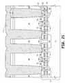
- the polysilicon storage nodes (capacitor bottom plates) 40are only minimally supported.
- the bottom plates 40 in the FIG. 6 structureeach comprise a first region 60 which defines a recess, and a second region 62 which defines an opening to the recess, with the first and second regions being continuous, each with the other.
- the bottom plate 40 of FIG. 6defines a receptacle having a rim 62 which defines an opening to the interior of the receptacle.
- the regions 60 , 62form vertically-oriented sides of the bottom plate, and the sides are electrically-coupled by a horizontally-oriented bottom 64 .
- a cell dielectric layer 70for example a layer of high-quality cell nitride, a polysilicon container capacitor top plate 72 , and a planar oxide layer such as BPSG 74 are formed according to means known in the art to result in the FIG. 7 structure.
- wafer processingcontinues according to means known in the art.
- FIG. 6It can be seen at the FIG. 6 structure that conventional processes remove the oxide 32 which supports the capacitor bottom plate 40 . This oxide removal is performed to allow formation of the cell dielectric and capacitor top plate on both sides of the bottom plate to form a double-sided capacitor.
- the structure of FIG. 6is easily damaged and susceptible to defects such as leaning (caused, for example, during the etch of BPSG 32 of FIG. 5 to result in FIG. 6 ), toppling, or lifting of the bottom plate.
- leaningcaused, for example, during the etch of BPSG 32 of FIG. 5 to result in FIG. 6
- etch tool technologycan etch contacts to a depth of about 3.0 micrometers ( ⁇ m) to about 3.5 ⁇ m. If the capacitor height causes the contact depth to go beyond the 3.0 ⁇ m to 3.5 ⁇ m limit, then additional masking layers will be needed. One way to do this is to form a portion of the contact to diffusion areas in the wafer before forming the capacitor, then forming the remaining portion after forming the capacitor. Such a process is complex and adds significantly to device cost.
- BPSG layer 32 of FIG. 5Another problem which can occur during conventional processing results indirectly from the etch of BPSG layer 32 of FIG. 5 to result in the FIG. 6 structure.
- BPSG over the device periphery(not depicted) is also etched, which forms a step in the oxide between the periphery, where there are no cell capacitors, and the array, where the tops of the cell capacitors are at the original level of the top of BPSG 32 .
- the periphery regionAfter forming the cell dielectric and top plate, the periphery region must be backfilled with oxide, which is then planarized. The requirement to backfill and planarize results in additional processing steps, which contributes to a further increase in costs.
- a method used to form a double-sided capacitor such as a container capacitor or a pedestal capacitorwhich reduces or eliminates one or more the problems described above, and a structure resulting therefrom, would be desirable.
- An embodiment of the present inventionprovides a new method which, among other advantages, reduces problems associated with the manufacture of semiconductor devices, particularly problems resulting from instability of unsupported capacitor bottom plates prior to formation of a supporting layer.
- Various embodiments of the present inventionprovide lateral support for a vertically-oriented structure, for example a storage capacitor such as a container capacitor or a pedestal capacitor.
- a storage capacitorsuch as a container capacitor or a pedestal capacitor.
- FIGS. 1-7are cross sections depicting a conventional method for forming a double-sided container, capacitor structure
- FIGS. 8-16 and 18 - 20are cross sections, and FIG. 17 is a plan view, depicting embodiments of the inventive method for forming a double-sided container capacitor structure;
- FIGS. 21 and 22are cross sections depicting an embodiment of the invention to form a pedestal capacitor
- FIG. 23is a block diagram of an exemplary use of the invention as a memory array in a dynamic random access memory.
- FIG. 24is an isometric depiction of a use of the invention in an electronic device.
- waferis to be understood as a semiconductor-based material including silicon, silicon-on-insulator (SOI) or silicon-on-sapphire (SOS) technology, doped and undoped semiconductors, epitaxial layers of silicon supported by a base semiconductor foundation, and other semiconductor structures.
- SOIsilicon-on-insulator
- SOSsilicon-on-sapphire
- doped and undoped semiconductorsepitaxial layers of silicon supported by a base semiconductor foundation, and other semiconductor structures.
- previous process stepsmay have been utilized to form regions or junctions in or over the base semiconductor structure or foundation.
- substrate assemblymay include a wafer with layers including dielectrics and conductors, and features such as transistors, formed thereover, depending on the particular stage of processing.
- the semiconductorneed not be silicon-based, but could be based on silicon-germanium, silicon-on-insulator, silicon-on-sapphire, germanium, or gallium arsenide, among others.
- the term “on” used with respect to two layers, one “on” the other,means at least some contact between the layers, while “over” means the layers are in close proximity, but possibly with one or more additional intervening layers such that contact is possible but not required. Neither “on” nor “over” implies any directionality as used herein.
- FIG. 8depicts a structure comprising a semiconductor wafer substrate assembly 10 comprising a semiconductor wafer 12 , conductively-doped regions 14 within the wafer, transistors comprising gate oxide 18 , a word line 20 , silicide 22 which enhances conductivity of the word line, a dielectric transistor capping layer 24 , dielectric spacers 26 , and conductive contact pads 28 .
- the contact pads 28reduce the amount of dielectric which must be removed during an etch of an overlying dielectric layer.
- Support layer 86 and sacrificial layer 88include etchability of layers 88 and 84 selective to layer 86 (i.e. layers 88 and 84 can be etched while removing none or very little of layer 86 ).
- Layer 86may comprise a second silicon nitride layer between about 200 ⁇ and about 1,200 ⁇ thick
- layer 88can comprise a silicon dioxide layer, for example using a BPSG or tetraethyl orthosilicate (TEOS) process, between about 300 ⁇ and about 600 ⁇ thick, preferably about 400 ⁇ .
- a patterned etch mask 90is formed having openings therein which allow an etch to expose contact pads 28 .
- the structure of FIG. 8is etched to remove the exposed portions of sacrificial layer 88 , support layer 86 , base dielectric layer 84 , and etch stop layer 31 , and to expose contact pads 28 and possibly a portion of capping layer 24 to result in a structure similar to FIG. 9 .
- a single etchcan initially be used to remove exposed portions of sacrificial silicon dioxide layer 88 , silicon nitride support layer 86 , and timed to stop within base dielectric layer 84 prior to exposing etch stop 31 . The chemistry can then be changed so that any remaining base dielectric layer 84 is removed while stopping on etch stop 31 .
- the etchcan be changed and performed for a time to sufficiently remove exposed portions of etch stop 31 which exposes contact pad 28 , while not excessively etching capping layer 24 or spacers 26 .
- the etch stop layer 31may also be left in place.
- photoresist layer 90is removed, along with any polymer (not depicted) or other contaminants which form during the etch, to result in the structure of FIG. 10 .
- a blanket conformal capacitor bottom plate layer 110such as titanium nitride is formed as depicted in FIG. 11 .
- a protective layer 112such as photoresist, is formed within the container to prevent contaminants from being deposited into the interior of the container formed by the bottom plate during subsequent processing.
- the structureis planarized, for example using chemical mechanical planarization (CMP) to result in the FIG. 12 structure.
- CMPchemical mechanical planarization
- sacrificial layer 88is selectively etched to expose the underlying support layer 86 , then protective layer 112 is removed.
- a sacrificial layer 88 of silicon dioxidecan be etched selective to a silicon nitride support layer 86 and a titanium nitride bottom plate layer 110 using a wet etch comprising hydrofluoric acid (HF).
- a protective layer 112 of photoresistcan be removed by ashing the material at a temperature of between about 150° C. and about 300° C., and then subjecting the ash to a wet etch, for example using hydrofluoric acid (HF) to remove the photoresist ash.
- HFhydrofluoric acid
- the etch of the sacrificial layer 88can be performed either before or after removal of protective layer 112 , if the etch is selective to the material of bottom plate 110 . If the etch of layer 88 is performed after removal of layer 112 , the etchant may traverse any pinholes or other voids within bottom plate layer 110 and begin to etch oxide layer 84 . This is not detrimental, however, as layer 84 will be removed during subsequent processing and provides no further critical function. The removal of protective layer 112 and sacrificial layer 88 results in the FIG. 13 structure.
- a masking spacer layer 140is formed over the surface of the FIG. 13 structure to result in the structure of FIG. 14 .
- the material selected for this layermust be able to withstand an etch of support layer 86 , and must also be etchable selective to the material of support layer 86 and bottom plates 110 . With a nitride support layer and titanium nitride bottom plates, polysilicon would function sufficiently.
- the masking spacer layeris formed to a thickness sufficient to fill in and impinge on itself in narrow regions 142 , and form conformally in the wider regions 144 .
- the narrow regions 142may have a width of between about 200 ⁇ and about 600 ⁇
- the wider regions 144may have a width of between about 600 ⁇ and about 1,200 ⁇ .
- the height of the exposed portions 146 of capacitor bottom plates 110which is determined by the thickness of sacrificial layer 88 , is between about 300 ⁇ and about 600 ⁇ .
- a conformal polysilicon layer 140is formed to have a target thickness of between about 200 ⁇ and about 500 ⁇ when measured over wide, flat surfaces.
- FIG. 14depicts layer 140 completely filling the recess in the bottom plates, but this may not occur, depending on the size of the opening within the bottom plate. However, enough material will likely form to prevent any damage to the bottom of plates 110 during a subsequent spacer etch of layer 140 described below.
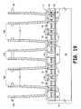
- an anisotropic spacer etchis performed on the masking spacer layer 140 to result in the FIG. 15 structure. This etch removes the material of the masking spacer layer 140 selective to the material of support layer 86 and bottom plates 110 . After etching layer 140 , spacers 150 remain in the wider regions 144 , while layer 152 remains to bridge the narrow regions 142 formed by adjacent bottom plates 110 .
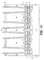
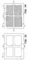
- FIG. 16is depicted in plan view along 1 - 1 of FIG. 17 , which depicts part of an array of container capacitor bottom plates 110 and the remaining portions 150 , 152 of the masking spacer layer 140 .
- FIG. 17Various capacitor layouts other than the one depicted in FIG. 17 can be used with the present invention. As this pattern of the masking layer defines the support layer 86 , the configuration of the support layer 86 is analogous to that of the masking spacer layer of FIG. 17 .
- the etch of the support layer 86 with this maskremoves the material of support layer 86 selective to the material of bottom plates 110 .
- the spacers 150 and support layer 86can also be etched during the same operation, but it is more likely that the spacers 150 will be etched during one process and the support layer 86 will be etched during another separate etch.
- a portion of polysilicon layer 140 and spacers 150may also be removed, as long as enough of these two features remain to allow exposure of BPSG 84 in the wide regions 144 and protection of support layer 86 in the narrow regions 142 .
- the remaining portions 140 , 150 , and 152 of the masking spacer layercan be removed at this point to result in the structure of FIG. 18 , or they may remain in place. If polysilicon spacers are removed, they can be etched selective to silicon nitride support layer 86 and titanium nitride bottom plates 110 using a wet etch comprising tetramethyl ammonium hydroxide (TMAH).
- TMAHtetramethyl ammonium hydroxide
- FIG. 19depicts the structure resulting from the removal of polysilicon features 140 , 150 , and 152 , and after etching of base dielectric layer 84 .
- the base dielectric layeris removed selective to support layer 86 , bottom plates 110 , and etch stop 31 .
- An etch which removes silicon dioxide selective to silicon nitride and titanium nitrideincludes a wet etch of hydrofluoric acid (HF) to result in the structure of FIG. 19 .
- the etchantcompletely removes the exposed base dielectric layer 84 depicted in FIG. 17 , and removes all of dielectric 84 around each capacitor bottom plate 110 .
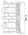
- support structures 86support the capacitors after removal of the base dielectric layer 84 . Removal of the base dielectric layer is necessary to allow the formation of a double-sided capacitor.
- These support structuresprovide a dielectric collar for each bottom plate, with each collar being continuous with adjacent collars such that the support layer forms a matrix which braces all capacitor bottom plates.
- the arrangement of the support layercan be determined from FIG. 17 , which depicts the pattern of masking spacer layer 150 , 152 , and also of the etched support layer 86 . As depicted in FIG. 19 , the top and bottom surfaces of support layer 86 are free from contact with any other layer.
- dielectric 84may remain, especially at the point of contact between the support layer 86 and the bottom plate 110 , which may be more difficult to clear completely. In any case, even if some of this dielectric 84 remains to contact the bottom side of layer 86 , the top and bottom surface of support layer 86 will remain generally free from contact with any other layer. It is conceivable that for some capacitor arrangements and processes the collar may not surround the capacitor bottom plate through 360° as depicted in FIG. 17 . Further, the bottom plates or other feature being supported by the collar may not be circular as depicted in FIG. 17 , but may be oval, ovoid, square, rectangular, etc. in shape.
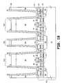
- a capacitor cell dielectric 200is formed according to means known in the art to form the structure of FIG. 20 .
- Wafer processingcontinues according to means known in the art.
- the completed structuremay have improved capacitance over conventional structures, because all of the base dielectric layer can be removed which allows the top plate to be formed along more of the bottom plate than conventional structures.
- a portion of base dielectric layer 32must remain in place to support the capacitors during formation of the cell dielectric and top plate.
- all of the base dielectric layercan be removed as depicted in FIG. 19 , because support layer 86 remains to brace the bottom plates.
- a mask layermay be formed prior to the etch of the sacrificial dielectric layer, prior to the etch of the masking spacer layer, or prior to the etch of the support layer. This will prevent etching of BPSG over the device periphery, which would form a step in the oxide between the periphery, where there are no storage cell capacitors, and the array, where the tops of the storage cell capacitors are at the original level of the top of layer 88 . If the periphery is not protected, the periphery must be backfilled with oxide which is then planarized, after forming the cell dielectric 200 and top plate 202 .
- a selective etchmay be performed on support layer 86 after forming spacers 152 of FIG. 16 to increase the width of the opening at 144 .
- This larger openingmay allow the base dielectric layer to be more easily removed, and may provide improved conditions for forming the cell dielectric layer 200 and capacitor top plate 202 .
- a pedestal capacitorcan be formed in a manner similar to the container capacitor as depicted by FIGS. 21 and 22 .
- the bottom plate layer 110is formed to completely fill the recessed defined by the sacrificial layer 88 , the support layer 86 , and the base dielectric layer 84 .
- the bottom plate layer 110will be much thicker than that depicted in the FIG. 11 structure.
- protective layer 112is not necessary, as bottom plate layer 110 completely fills the recess.
- the bottom plate layer 110 and possibly a portion of the sacrificial layer 88is planarized to remove layer 110 from the horizontal surface of sacrificial layer 88 to leave the pedestal capacitor bottom plate 110 as depicted in FIG. 22 .
- a single layer of materialmay be formed instead of forming both the sacrificial layer 88 and the support layer 86 of FIG. 12 .
- This single layerwould be a thicker layer of the material of the support layer, such as silicon nitride, and would be as thick as layers 86 and 88 combined.
- a timed etchwould be performed on this layer to result in the structure of FIG. 13 .
- This processis not as controllable as using two separate layers and is therefore not as preferable for most process flows, but may have advantages for some processes. Processing then continues according to the other embodiments, for example to form the masking spacer layer 140 and other subsequent steps.
- FIG. 23is a plan view depicting four arrays 230 and a periphery 232 of a semiconductor die 234 prior to forming the patterned resist layer 90 of FIG. 8 .
- a typical memory diewill likely comprise a larger number of arrays.
- This moatwill be filled with material during the formation of the capacitor bottom plate 110 , and thus no additional processing is required to form and fill the moat.
- the moatmay be between about 200 ⁇ and about 600 ⁇ wide.
- a photoresist layerwould be formed to cover and protect the periphery but to expose the array.
- the photoresist layer and the layer within the moatthereby protects the dielectric layer such as BPSG in the periphery from being etched during the removal of the base dielectric layer which exposes the sidewalls of the capacitor bottom plates.
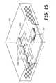
- a semiconductor device 250 formed in accordance with the inventionmay be attached along with other devices such as a microprocessor 252 to a printed circuit board 254 , for example to a computer motherboard or as a part of a memory module used in a personal computer, a minicomputer, or a mainframe 256 .
- FIG. 25may also represent use of device 250 in other electronic devices comprising a housing 236 , for example devices comprising a microprocessor 252 , related to telecommunications, the automobile industry, semiconductor test and manufacturing equipment, consumer electronics, or virtually any piece of consumer or industrial electronic equipment.
- FIG. 26is a simplified block diagram of a memory device such as a dynamic random access memory having a memory array with container capacitors which may be formed using an embodiment of the present invention.
- FIG. 26depicts a processor 260 coupled to a memory device 262 , and further depicts the following basic sections of a memory integrated circuit: control circuitry 264 ; row 266 and column 268 address buffers; row 270 and column 272 decoders; sense amplifiers 274 ; memory array 276 ; and data input/output 278 .
Landscapes
- Engineering & Computer Science (AREA)
- Manufacturing & Machinery (AREA)
- Semiconductor Memories (AREA)
- Semiconductor Integrated Circuits (AREA)
- Chemical Vapour Deposition (AREA)
Abstract
Description
- This invention relates to the field of semiconductor manufacture and, more particularly, to a method for forming a double-sided capacitor having lateral support for its capacitor bottom plate.
- During the manufacture of semiconductor devices which comprise memory elements, such as dynamic random access memories (DRAMs), static random access memories (SRAMs), and some microprocessors, capacitors such as container capacitors and pedestal capacitors are commonly formed. Container and pedestal capacitors are well known to allow an increased stored charge over planar capacitors by increasing the surface area on which the charge may be stored.
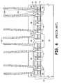
FIGS. 1-7 depict a conventional method for forming a plurality of container capacitors from polysilicon. Formation of a pedestal capacitor is similar, but the bottom plate is a solid plug and the cell dielectric and top plate are conformal with the exterior of the bottom plate to form a single-sided vertically-oriented capacitor.FIG. 1 depicts a semiconductorwafer substrate assembly 10 comprising asemiconductor wafer 12 having a plurality of doped source/drain regions 14 within thewafer 12.FIG. 1 further depictstransistors 16 comprisinggate oxide 18, a dopedpolysilicon control gate 20,silicide 22 such as tungsten silicide which increases conductivity of thecontrol gate 20, and acapping layer 24 often manufactured from silicon nitride.Silicon nitride spacers 26 are formed to insulate thecontrol gate 20 andsilicide 22 frompolysilicon pads 28 to which the container capacitors will be electrically coupled. Shallow trench isolation (STI, field oxide)30 reduces unwanted electrical interaction between adjacent control gates. Anetch stop layer 31 is formed, then a thick layer of depositedoxide 32 such as borophosphosilicate glass (BPSG) formed to provide a base dielectric layer for capacitor features which are formed later. A patternedphotoresist layer 34 defines the location of the container capacitors to be formed. TheFIG. 1 structure may further include one or more bit (digit) lines under the BPSG layer or various other structural elements or differences which, for simplicity of explanation, have not been depicted.- The
FIG. 1 structure is subjected to an anisotropic etch which removes the exposed portions of the BPSG layer to expose theetch stop layer 31 and to form a patterned BPSG layer which provides a base dielectric having recesses for the capacitors. The exposed portion of the etch stop is the removed. Subsequent to the etch of etch stop31 thepolysilicon pads 28 and possibly a portion ofcapping layer 24 are exposed to result in a structure similar toFIG. 2 . The remainingphotoresist layer 34 is stripped and any polymer (not depicted) which forms during the etch is removed according to means known in the art to provide theFIG. 3 structure. - As depicted in
FIG. 4 , a blanketconductive layer 40 such as polysilicon or another material is formed conformal with the deposited oxide layer, and will provide a capacitor storage node for the completed capacitor. A thickblanket filler material 42, such as photoresist, is formed to fill the containers provided bypolysilicon 40. TheFIG. 4 structure is then subjected to a planarizing process, such as a chemical planarization, a mechanical planarization, or a chemical mechanical planarization (CMP) step. This process removes portions of thephotoresist 42, thepolysilicon 40, and usually a portion of theBPSG 32 to result in theFIG. 5 structure. - Next, the
BPSG 32 is partially etched with an etch selective to polysilicon (i.e. an etch which minimally etches or, preferably, doesn't etch polysilicon) to result in the structure ofFIG. 6 . At this point in the process the polysilicon storage nodes (capacitor bottom plates)40 are only minimally supported. Thebottom plates 40 in theFIG. 6 structure each comprise afirst region 60 which defines a recess, and a second region62 which defines an opening to the recess, with the first and second regions being continuous, each with the other. In other words, thebottom plate 40 ofFIG. 6 defines a receptacle having a rim62 which defines an opening to the interior of the receptacle. Theregions 60,62 form vertically-oriented sides of the bottom plate, and the sides are electrically-coupled by a horizontally-oriented bottom 64. - Next, a cell
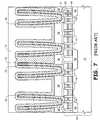
dielectric layer 70, for example a layer of high-quality cell nitride, a polysilicon containercapacitor top plate 72, and a planar oxide layer such as BPSG74 are formed according to means known in the art to result in theFIG. 7 structure. This forms a “double-sided” capacitor, as both the capacitor cell dielectric70 andcapacitor top plate 72 follow the contours of the majority of both the inside and outside of each containercapacitor bottom plate 40. After forming the structure ofFIG. 7 , wafer processing continues according to means known in the art. - It can be seen at the
FIG. 6 structure that conventional processes remove theoxide 32 which supports thecapacitor bottom plate 40. This oxide removal is performed to allow formation of the cell dielectric and capacitor top plate on both sides of the bottom plate to form a double-sided capacitor. The structure ofFIG. 6 is easily damaged and susceptible to defects such as leaning (caused, for example, during the etch ofBPSG 32 ofFIG. 5 to result inFIG. 6 ), toppling, or lifting of the bottom plate. However, it is desirable to form a double-sided capacitor to increase the cell capacitance which allows the cell height to be decreased over a single sided capacitor. Limiting this vertical dimension of the cell capacitor is desirable because it sets the depth of the contact level to follow. For example, current etch tool technology can etch contacts to a depth of about 3.0 micrometers (μm) to about 3.5 μm. If the capacitor height causes the contact depth to go beyond the 3.0 μm to 3.5 μm limit, then additional masking layers will be needed. One way to do this is to form a portion of the contact to diffusion areas in the wafer before forming the capacitor, then forming the remaining portion after forming the capacitor. Such a process is complex and adds significantly to device cost. - Another problem which can occur during conventional processing results indirectly from the etch of
BPSG layer 32 ofFIG. 5 to result in theFIG. 6 structure. During this etch, BPSG over the device periphery (not depicted) is also etched, which forms a step in the oxide between the periphery, where there are no cell capacitors, and the array, where the tops of the cell capacitors are at the original level of the top ofBPSG 32. After forming the cell dielectric and top plate, the periphery region must be backfilled with oxide, which is then planarized. The requirement to backfill and planarize results in additional processing steps, which contributes to a further increase in costs. - A method used to form a double-sided capacitor such as a container capacitor or a pedestal capacitor which reduces or eliminates one or more the problems described above, and a structure resulting therefrom, would be desirable.
- An embodiment of the present invention provides a new method which, among other advantages, reduces problems associated with the manufacture of semiconductor devices, particularly problems resulting from instability of unsupported capacitor bottom plates prior to formation of a supporting layer.
- Various embodiments of the present invention provide lateral support for a vertically-oriented structure, for example a storage capacitor such as a container capacitor or a pedestal capacitor.
- Additional advantages will become apparent to those skilled in the art from the following detailed description read in conjunction with the appended claims and the drawings attached hereto.
FIGS. 1-7 are cross sections depicting a conventional method for forming a double-sided container, capacitor structure;FIGS. 8-16 and18-20 are cross sections, andFIG. 17 is a plan view, depicting embodiments of the inventive method for forming a double-sided container capacitor structure;FIGS. 21 and 22 are cross sections depicting an embodiment of the invention to form a pedestal capacitor;FIG. 23 is a block diagram of an exemplary use of the invention as a memory array in a dynamic random access memory; andFIG. 24 is an isometric depiction of a use of the invention in an electronic device.- It should be emphasized that the drawings herein may not be to exact scale and are schematic representations. The drawings are not intended to portray the specific parameters, materials, particular uses, or the structural details of the invention, which can be determined by one of skill in the art by examination of the information herein.
- The term “wafer” is to be understood as a semiconductor-based material including silicon, silicon-on-insulator (SOI) or silicon-on-sapphire (SOS) technology, doped and undoped semiconductors, epitaxial layers of silicon supported by a base semiconductor foundation, and other semiconductor structures. Furthermore, when reference is made to a “wafer” in the following description, previous process steps may have been utilized to form regions or junctions in or over the base semiconductor structure or foundation. Additionally, when reference is made to a “substrate assembly” in the following description, the substrate assembly may include a wafer with layers including dielectrics and conductors, and features such as transistors, formed thereover, depending on the particular stage of processing. In addition, the semiconductor need not be silicon-based, but could be based on silicon-germanium, silicon-on-insulator, silicon-on-sapphire, germanium, or gallium arsenide, among others. Further, in the discussion and claims herein, the term “on” used with respect to two layers, one “on” the other, means at least some contact between the layers, while “over” means the layers are in close proximity, but possibly with one or more additional intervening layers such that contact is possible but not required. Neither “on” nor “over” implies any directionality as used herein.
- A first embodiment of an inventive method used during the formation of a semiconductor device, and various inventive in-process structures, are depicted in
FIGS. 8-20 .FIG. 8 depicts a structure comprising a semiconductorwafer substrate assembly 10 comprising asemiconductor wafer 12, conductively-dopedregions 14 within the wafer, transistors comprisinggate oxide 18, aword line 20,silicide 22 which enhances conductivity of the word line, a dielectrictransistor capping layer 24,dielectric spacers 26, andconductive contact pads 28. Thecontact pads 28 reduce the amount of dielectric which must be removed during an etch of an overlying dielectric layer. - After forming the features of the
wafer substrate assembly 10, a blanketetch stop layer 31 is formed. Theetch stop layer 31 may comprise a layer of silicon nitride, silicon carbon (Si.C), aluminum oxide (Al2O3), or another material between about 50 angstroms (Å) and about 1,000 Å thick. Next, abase dielectric layer 84, for example borophosphosilicate glass (BPSG), phosphosilicate glass (PSG), spun-on dielectric (SOD), or undoped silicate glass (USG), is formed overetch stop layer 31. Ablanket support layer 86 and a blanketsacrificial layer 88 are formed over thebase dielectric layer 84. Properties ofsupport layer 86 andsacrificial layer 88 include etchability oflayers Layer 86 may comprise a second silicon nitride layer between about 200 Å and about 1,200 Å thick, andlayer 88 can comprise a silicon dioxide layer, for example using a BPSG or tetraethyl orthosilicate (TEOS) process, between about 300 Å and about 600 Å thick, preferably about 400 Å. Next, apatterned etch mask 90 is formed having openings therein which allow an etch to exposecontact pads 28. - After forming
mask layer 90, the structure ofFIG. 8 is etched to remove the exposed portions ofsacrificial layer 88,support layer 86,base dielectric layer 84, and etchstop layer 31, and to exposecontact pads 28 and possibly a portion of cappinglayer 24 to result in a structure similar toFIG. 9 . A single etch can initially be used to remove exposed portions of sacrificialsilicon dioxide layer 88, siliconnitride support layer 86, and timed to stop withinbase dielectric layer 84 prior to exposingetch stop 31. The chemistry can then be changed so that any remainingbase dielectric layer 84 is removed while stopping onetch stop 31. Then, optionally, the etch can be changed and performed for a time to sufficiently remove exposed portions of etch stop31 which exposescontact pad 28, while not excessively etching cappinglayer 24 orspacers 26. Theetch stop layer 31 may also be left in place. - After forming the
FIG. 9 structure,photoresist layer 90 is removed, along with any polymer (not depicted) or other contaminants which form during the etch, to result in the structure ofFIG. 10 . - Next, a blanket conformal capacitor
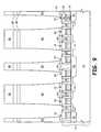
bottom plate layer 110 such as titanium nitride is formed as depicted inFIG. 11 . Aprotective layer 112 such as photoresist, is formed within the container to prevent contaminants from being deposited into the interior of the container formed by the bottom plate during subsequent processing. After formingbottom plate layer 110 andprotective layer 112, the structure is planarized, for example using chemical mechanical planarization (CMP) to result in theFIG. 12 structure. - After forming the structure of
FIG. 12 ,sacrificial layer 88 is selectively etched to expose theunderlying support layer 86, thenprotective layer 112 is removed. For example, asacrificial layer 88 of silicon dioxide can be etched selective to a siliconnitride support layer 86 and a titanium nitridebottom plate layer 110 using a wet etch comprising hydrofluoric acid (HF). Likewise, aprotective layer 112 of photoresist can be removed by ashing the material at a temperature of between about 150° C. and about 300° C., and then subjecting the ash to a wet etch, for example using hydrofluoric acid (HF) to remove the photoresist ash. The etch of thesacrificial layer 88 can be performed either before or after removal ofprotective layer 112, if the etch is selective to the material ofbottom plate 110. If the etch oflayer 88 is performed after removal oflayer 112, the etchant may traverse any pinholes or other voids withinbottom plate layer 110 and begin to etchoxide layer 84. This is not detrimental, however, aslayer 84 will be removed during subsequent processing and provides no further critical function. The removal ofprotective layer 112 andsacrificial layer 88 results in theFIG. 13 structure. - Next, a masking
spacer layer 140 is formed over the surface of theFIG. 13 structure to result in the structure ofFIG. 14 . The material selected for this layer must be able to withstand an etch ofsupport layer 86, and must also be etchable selective to the material ofsupport layer 86 andbottom plates 110. With a nitride support layer and titanium nitride bottom plates, polysilicon would function sufficiently. The masking spacer layer is formed to a thickness sufficient to fill in and impinge on itself innarrow regions 142, and form conformally in thewider regions 144. With current technology, thenarrow regions 142 may have a width of between about 200 Å and about 600 Å, thewider regions 144 may have a width of between about 600 Å and about 1,200 Å. The height of the exposedportions 146 ofcapacitor bottom plates 110, which is determined by the thickness ofsacrificial layer 88, is between about 300 Å and about 600 Å. To result in the structure ofFIG. 14 , aconformal polysilicon layer 140 is formed to have a target thickness of between about 200 Å and about 500 Å when measured over wide, flat surfaces.FIG. 14 depictslayer 140 completely filling the recess in the bottom plates, but this may not occur, depending on the size of the opening within the bottom plate. However, enough material will likely form to prevent any damage to the bottom ofplates 110 during a subsequent spacer etch oflayer 140 described below. - Next, an anisotropic spacer etch is performed on the masking
spacer layer 140 to result in theFIG. 15 structure. This etch removes the material of the maskingspacer layer 140 selective to the material ofsupport layer 86 andbottom plates 110. After etchinglayer 140,spacers 150 remain in thewider regions 144, whilelayer 152 remains to bridge thenarrow regions 142 formed byadjacent bottom plates 110. - After forming
spacers 150, thesupport layer 86 is etched using thespacers 150 and the other remainingportions 152 oflayer 140 as a mask to result in theFIG. 16 structure.FIG. 16 is depicted in plan view along1-1 ofFIG. 17 , which depicts part of an array of containercapacitor bottom plates 110 and the remainingportions spacer layer 140. Various capacitor layouts other than the one depicted inFIG. 17 can be used with the present invention. As this pattern of the masking layer defines thesupport layer 86, the configuration of thesupport layer 86 is analogous to that of the masking spacer layer ofFIG. 17 . The etch of thesupport layer 86 with this mask removes the material ofsupport layer 86 selective to the material ofbottom plates 110. Thespacers 150 andsupport layer 86 can also be etched during the same operation, but it is more likely that thespacers 150 will be etched during one process and thesupport layer 86 will be etched during another separate etch. During the etch of support layer86 a portion ofpolysilicon layer 140 andspacers 150 may also be removed, as long as enough of these two features remain to allow exposure ofBPSG 84 in thewide regions 144 and protection ofsupport layer 86 in thenarrow regions 142. - The remaining
portions FIG. 18 , or they may remain in place. If polysilicon spacers are removed, they can be etched selective to siliconnitride support layer 86 and titaniumnitride bottom plates 110 using a wet etch comprising tetramethyl ammonium hydroxide (TMAH). FIG. 19 depicts the structure resulting from the removal of polysilicon features140,150, and152, and after etching ofbase dielectric layer 84. The base dielectric layer is removed selective to supportlayer 86,bottom plates 110, and etchstop 31. An etch which removes silicon dioxide selective to silicon nitride and titanium nitride includes a wet etch of hydrofluoric acid (HF) to result in the structure ofFIG. 19 . The etchant completely removes the exposedbase dielectric layer 84 depicted inFIG. 17 , and removes all of dielectric84 around eachcapacitor bottom plate 110.- As depicted in the
FIG. 19 structure,support structures 86 support the capacitors after removal of thebase dielectric layer 84. Removal of the base dielectric layer is necessary to allow the formation of a double-sided capacitor. These support structures provide a dielectric collar for each bottom plate, with each collar being continuous with adjacent collars such that the support layer forms a matrix which braces all capacitor bottom plates. The arrangement of the support layer can be determined fromFIG. 17 , which depicts the pattern of maskingspacer layer support layer 86. As depicted inFIG. 19 , the top and bottom surfaces ofsupport layer 86 are free from contact with any other layer. However, some of dielectric84 may remain, especially at the point of contact between thesupport layer 86 and thebottom plate 110, which may be more difficult to clear completely. In any case, even if some of this dielectric84 remains to contact the bottom side oflayer 86, the top and bottom surface ofsupport layer 86 will remain generally free from contact with any other layer. It is conceivable that for some capacitor arrangements and processes the collar may not surround the capacitor bottom plate through 360° as depicted inFIG. 17 . Further, the bottom plates or other feature being supported by the collar may not be circular as depicted inFIG. 17 , but may be oval, ovoid, square, rectangular, etc. in shape. - If the remaining
portions spacer layer 140 have not yet been removed, they must be removed at this point to prevent shorting between capacitor bottom plates. - Finally, a
capacitor cell dielectric 200, a capacitortop plate 202, and adielectric layer 204 are formed according to means known in the art to form the structure ofFIG. 20 . Wafer processing continues according to means known in the art. - The completed structure may have improved capacitance over conventional structures, because all of the base dielectric layer can be removed which allows the top plate to be formed along more of the bottom plate than conventional structures. Referring to
FIG. 6 , for example, a portion ofbase dielectric layer 32 must remain in place to support the capacitors during formation of the cell dielectric and top plate. With an embodiment of the present invention, however, all of the base dielectric layer can be removed as depicted inFIG. 19 , becausesupport layer 86 remains to brace the bottom plates. - To prevent etching of the periphery, a mask layer may be formed prior to the etch of the sacrificial dielectric layer, prior to the etch of the masking spacer layer, or prior to the etch of the support layer. This will prevent etching of BPSG over the device periphery, which would form a step in the oxide between the periphery, where there are no storage cell capacitors, and the array, where the tops of the storage cell capacitors are at the original level of the top of
layer 88. If the periphery is not protected, the periphery must be backfilled with oxide which is then planarized, after forming thecell dielectric 200 andtop plate 202. - A selective etch may be performed on
support layer 86 after formingspacers 152 ofFIG. 16 to increase the width of the opening at144. This larger opening may allow the base dielectric layer to be more easily removed, and may provide improved conditions for forming thecell dielectric layer 200 and capacitortop plate 202. - A pedestal capacitor can be formed in a manner similar to the container capacitor as depicted by
FIGS. 21 and 22 . As depicted inFIG. 21 , thebottom plate layer 110 is formed to completely fill the recessed defined by thesacrificial layer 88, thesupport layer 86, and thebase dielectric layer 84. Thus thebottom plate layer 110 will be much thicker than that depicted in theFIG. 11 structure. In this pedestal capacitor embodiment,protective layer 112 is not necessary, asbottom plate layer 110 completely fills the recess. After forming theFIG. 21 structure, thebottom plate layer 110 and possibly a portion of thesacrificial layer 88 is planarized to removelayer 110 from the horizontal surface ofsacrificial layer 88 to leave the pedestalcapacitor bottom plate 110 as depicted inFIG. 22 . - In another embodiment, a single layer of material may be formed instead of forming both the
sacrificial layer 88 and thesupport layer 86 ofFIG. 12 . This single layer would be a thicker layer of the material of the support layer, such as silicon nitride, and would be as thick aslayers FIG. 13 . This process is not as controllable as using two separate layers and is therefore not as preferable for most process flows, but may have advantages for some processes. Processing then continues according to the other embodiments, for example to form the maskingspacer layer 140 and other subsequent steps. - With the above embodiments of the invention it may be necessary to protect the peripheral area of the die during processing of the array of capacitors, especially during the etch of the base dielectric of the
FIG. 18 structure to form theFIG. 19 structure.FIG. 23 is a plan view depicting fourarrays 230 and aperiphery 232 of asemiconductor die 234 prior to forming the patterned resistlayer 90 ofFIG. 8 . A typical memory die will likely comprise a larger number of arrays. FIG. 24 depicts theFIG. 23 structure after forming patternedphotoresist layer 90. Resistlayer 90 has openings therein240 which will allow the etch of thesacrificial layer 88, thesupport layer 86, and thebase dielectric layer 84 of theFIG. 8 structure to form theFIG. 9 structure.FIG. 24 is not to scale, and manymore openings 240 for capacitors will be formed than are depicted. Resistlayer 90 also has openings therein242 which form a “moat” around the array which will protect theperiphery 232 during the removal ofbase dielectric layer 84 to form theFIG. 19 structure. This moat will be filled with material during the formation of thecapacitor bottom plate 110, and thus no additional processing is required to form and fill the moat. For current processing, the moat may be between about 200 Å and about 600 Å wide. During the etch of the base dielectric through the collar, a photoresist layer would be formed to cover and protect the periphery but to expose the array. The photoresist layer and the layer within the moat thereby protects the dielectric layer such as BPSG in the periphery from being etched during the removal of the base dielectric layer which exposes the sidewalls of the capacitor bottom plates.- As depicted in
FIG. 25 , asemiconductor device 250 formed in accordance with the invention may be attached along with other devices such as amicroprocessor 252 to a printedcircuit board 254, for example to a computer motherboard or as a part of a memory module used in a personal computer, a minicomputer, or amainframe 256.FIG. 25 may also represent use ofdevice 250 in other electronic devices comprising a housing236, for example devices comprising amicroprocessor 252, related to telecommunications, the automobile industry, semiconductor test and manufacturing equipment, consumer electronics, or virtually any piece of consumer or industrial electronic equipment. - The process and structure described herein can be used to manufacture a number of different structures which comprise a capacitor such as a container capacitor or a pedestal capacitor.
FIG. 26 , for example, is a simplified block diagram of a memory device such as a dynamic random access memory having a memory array with container capacitors which may be formed using an embodiment of the present invention. The general operation of such a device is known to one skilled in the art.FIG. 26 depicts aprocessor 260 coupled to amemory device 262, and further depicts the following basic sections of a memory integrated circuit:control circuitry 264;row 266 andcolumn 268 address buffers;row 270 andcolumn 272 decoders;sense amplifiers 274;memory array 276; and data input/output 278. - While this invention has been described with reference to illustrative embodiments, this description is not meant to be construed in a limiting sense. Various modifications of the illustrative embodiments, as well as additional embodiments of the invention, will be apparent to persons skilled in the art upon reference to this description. It is therefore contemplated that the appended claims will cover any such modifications or embodiments as fall within the true scope of the invention.
Claims (7)
Priority Applications (2)
| Application Number | Priority Date | Filing Date | Title |
|---|---|---|---|
| US11/077,388US7655968B2 (en) | 2003-09-04 | 2005-03-10 | Semiconductor devices |
| US12/689,955US8786001B2 (en) | 2003-09-04 | 2010-01-19 | Semiconductor devices |
Applications Claiming Priority (2)
| Application Number | Priority Date | Filing Date | Title |
|---|---|---|---|
| US10/656,732US7067385B2 (en) | 2003-09-04 | 2003-09-04 | Support for vertically oriented capacitors during the formation of a semiconductor device |
| US11/077,388US7655968B2 (en) | 2003-09-04 | 2005-03-10 | Semiconductor devices |
Related Parent Applications (1)
| Application Number | Title | Priority Date | Filing Date |
|---|---|---|---|
| US10/656,732DivisionUS7067385B2 (en) | 2003-09-04 | 2003-09-04 | Support for vertically oriented capacitors during the formation of a semiconductor device |
Related Child Applications (1)
| Application Number | Title | Priority Date | Filing Date |
|---|---|---|---|
| US12/689,955ContinuationUS8786001B2 (en) | 2003-09-04 | 2010-01-19 | Semiconductor devices |
Publications (2)
| Publication Number | Publication Date |
|---|---|
| US20050158949A1true US20050158949A1 (en) | 2005-07-21 |
| US7655968B2 US7655968B2 (en) | 2010-02-02 |
Family
ID=34226414
Family Applications (3)
| Application Number | Title | Priority Date | Filing Date |
|---|---|---|---|
| US10/656,732Expired - Fee RelatedUS7067385B2 (en) | 2003-09-04 | 2003-09-04 | Support for vertically oriented capacitors during the formation of a semiconductor device |
| US11/077,388Expired - Fee RelatedUS7655968B2 (en) | 2003-09-04 | 2005-03-10 | Semiconductor devices |
| US12/689,955Expired - Fee RelatedUS8786001B2 (en) | 2003-09-04 | 2010-01-19 | Semiconductor devices |
Family Applications Before (1)
| Application Number | Title | Priority Date | Filing Date |
|---|---|---|---|
| US10/656,732Expired - Fee RelatedUS7067385B2 (en) | 2003-09-04 | 2003-09-04 | Support for vertically oriented capacitors during the formation of a semiconductor device |
Family Applications After (1)
| Application Number | Title | Priority Date | Filing Date |
|---|---|---|---|
| US12/689,955Expired - Fee RelatedUS8786001B2 (en) | 2003-09-04 | 2010-01-19 | Semiconductor devices |
Country Status (8)
| Country | Link |
|---|---|
| US (3) | US7067385B2 (en) |
| EP (2) | EP1665372B1 (en) |
| JP (1) | JP4512880B2 (en) |
| KR (1) | KR20060064662A (en) |
| CN (1) | CN100587941C (en) |
| AT (1) | ATE510301T1 (en) |
| TW (1) | TWI239633B (en) |
| WO (1) | WO2005024936A2 (en) |
Cited By (35)
| Publication number | Priority date | Publication date | Assignee | Title |
|---|---|---|---|---|
| US20050093046A1 (en)* | 2003-11-03 | 2005-05-05 | Tae-Hyuk Ahn | Plurality of capacitors employing holding layer patterns and method of fabricating the same |
| US20060121672A1 (en)* | 2004-12-06 | 2006-06-08 | Cem Basceri | Methods of forming pluralities of capacitors, and integrated circuitry |
| US20060148190A1 (en)* | 2004-08-30 | 2006-07-06 | Busch Brett W | Methods of forming a plurality of capacitors |
| US20070134872A1 (en)* | 2005-08-02 | 2007-06-14 | Sandhu Gurtej S | Methods of forming pluralities of capacitors |
| US20070161202A1 (en)* | 2004-08-27 | 2007-07-12 | Manning H M | Methods of forming a plurality of capacitors |
| US20070196978A1 (en)* | 2005-05-18 | 2007-08-23 | Manning H M | Integrated circuitry comprising a pair of adjacent capacitors |
| US20070207622A1 (en)* | 2006-02-23 | 2007-09-06 | Micron Technology, Inc. | Highly selective doped oxide etchant |
| US20070238259A1 (en)* | 2006-04-10 | 2007-10-11 | Micron Technology, Inc. | Methods of forming a plurality of capacitors |
| US20070275553A1 (en)* | 2006-05-25 | 2007-11-29 | Elpida Memory, Inc. | Method for manufacturing semiconductor device |
| US20080090416A1 (en)* | 2006-10-11 | 2008-04-17 | Micro Technology, Inc. | Methods of etching polysilicon and methods of forming pluralities of capacitors |
| US7413952B2 (en) | 2004-08-27 | 2008-08-19 | Micron Technology, Inc. | Methods of forming a plurality of circuit components and methods of forming a plurality of structures suspended elevationally above a substrate |
| US20080206950A1 (en)* | 2007-02-26 | 2008-08-28 | Micron Technology, Inc. | Methods of forming a plurality of capacitors |
| US20090047769A1 (en)* | 2007-08-13 | 2009-02-19 | Vishwanath Bhat | Methods of Forming a Plurality of Capacitors |
| US20090209080A1 (en)* | 2005-03-18 | 2009-08-20 | Sandhu Gurtej S | Methods of Forming Pluralities of Capacitors |
| US7585741B2 (en) | 2004-07-19 | 2009-09-08 | Micron Technology, Inc. | Methods of forming capacitors |
| US20090239343A1 (en)* | 2006-07-17 | 2009-09-24 | Fernando Gonzalez | Methods Of Forming Lines Of Capacitorless One Transistor DRAM Cells, Methods Of Patterning Substrates, And Methods Of Forming Two Conductive Lines |
| US20100009512A1 (en)* | 2008-07-09 | 2010-01-14 | Fred Fishburn | Methods of forming a plurality of capacitors |
| US20100012989A1 (en)* | 2008-07-18 | 2010-01-21 | Hynix Semiconductor Inc. | Semiconductor device and method of fabricating the same |
| US20100099232A1 (en)* | 2008-10-16 | 2010-04-22 | Niraj Rana | Methods Of Forming Capacitors, And Methods Of Utilizing Silicon Dioxide-Containing Masking Structures |
| US20100117196A1 (en)* | 2003-09-04 | 2010-05-13 | Manning Homer M | Support For Vertically-Oriented Capacitors During The Formation of a Semiconductor Device |
| US20120038052A1 (en)* | 2010-08-10 | 2012-02-16 | Nanya Technology Corporation | Semiconductor device and fabricating method thereof |
| US8120101B2 (en) | 2004-09-01 | 2012-02-21 | Micron Technology, Inc. | Semiconductor constructions and transistors, and methods of forming semiconductor constructions and transistors |
| US20120064680A1 (en)* | 2010-09-15 | 2012-03-15 | Oh Jung-Min | Methods of forming a capacitor structure and methods of manufacturing semiconductor devices using the same |
| US8274777B2 (en) | 2008-04-08 | 2012-09-25 | Micron Technology, Inc. | High aspect ratio openings |
| US8388851B2 (en) | 2008-01-08 | 2013-03-05 | Micron Technology, Inc. | Capacitor forming methods |
| US8389363B2 (en) | 2006-02-02 | 2013-03-05 | Micron Technology, Inc. | Methods of forming field effect transistors, methods of forming field effect transistor gates, methods of forming integrated circuitry comprising a transistor gate array and circuitry peripheral to the gate array, and methods of forming integrated circuitry comprising a transistor gate array including first gates and second grounded isolation gates |
| US8394699B2 (en) | 2006-08-21 | 2013-03-12 | Micron Technology, Inc. | Memory arrays and methods of fabricating memory arrays |
| US8399920B2 (en) | 2005-07-08 | 2013-03-19 | Werner Juengling | Semiconductor device comprising a transistor gate having multiple vertically oriented sidewalls |
| US8426273B2 (en) | 2005-08-30 | 2013-04-23 | Micron Technology, Inc. | Methods of forming field effect transistors on substrates |
| US8446762B2 (en) | 2006-09-07 | 2013-05-21 | Micron Technology, Inc. | Methods of making a semiconductor memory device |
| US8518788B2 (en) | 2010-08-11 | 2013-08-27 | Micron Technology, Inc. | Methods of forming a plurality of capacitors |
| US8652926B1 (en) | 2012-07-26 | 2014-02-18 | Micron Technology, Inc. | Methods of forming capacitors |
| US8946043B2 (en) | 2011-12-21 | 2015-02-03 | Micron Technology, Inc. | Methods of forming capacitors |
| US9076680B2 (en) | 2011-10-18 | 2015-07-07 | Micron Technology, Inc. | Integrated circuitry, methods of forming capacitors, and methods of forming integrated circuitry comprising an array of capacitors and circuitry peripheral to the array |
| US10515801B2 (en) | 2007-06-04 | 2019-12-24 | Micron Technology, Inc. | Pitch multiplication using self-assembling materials |
Families Citing this family (101)
| Publication number | Priority date | Publication date | Assignee | Title |
|---|---|---|---|---|
| US7057256B2 (en) | 2001-05-25 | 2006-06-06 | President & Fellows Of Harvard College | Silicon-based visible and near-infrared optoelectric devices |
| US7442629B2 (en) | 2004-09-24 | 2008-10-28 | President & Fellows Of Harvard College | Femtosecond laser-induced formation of submicrometer spikes on a semiconductor substrate |
| US7125781B2 (en) | 2003-09-04 | 2006-10-24 | Micron Technology, Inc. | Methods of forming capacitor devices |
| KR100546395B1 (en)* | 2003-11-17 | 2006-01-26 | 삼성전자주식회사 | Capacitor of Semiconductor Device and Manufacturing Method Thereof |
| KR100553835B1 (en)* | 2004-01-26 | 2006-02-24 | 삼성전자주식회사 | Capacitor and manufacturing method thereof |
| KR100568733B1 (en)* | 2004-02-10 | 2006-04-07 | 삼성전자주식회사 | Capacitors having improved structural stability, methods of manufacturing the same, and semiconductor devices including the same, and methods of manufacturing the same |
| EP1732134B1 (en)* | 2004-02-27 | 2012-10-24 | National University Corporation Tohoku Unversity | Solid-state imagine device, line sensor, optical sensor, and method for operating solid-state imaging device |
| KR100545866B1 (en)* | 2004-04-27 | 2006-01-24 | 삼성전자주식회사 | Capacitor and manufacturing method thereof |
| US20070037349A1 (en)* | 2004-04-30 | 2007-02-15 | Martin Gutsche | Method of forming electrodes |
| KR100533959B1 (en)* | 2004-06-30 | 2005-12-06 | 삼성전자주식회사 | Method for manufacturing semiconductor device |
| KR100655751B1 (en)* | 2004-10-01 | 2006-12-11 | 삼성전자주식회사 | Manufacturing Method of Semiconductor Device |
| KR100752642B1 (en)* | 2005-02-02 | 2007-08-29 | 삼성전자주식회사 | Capacitor Manufacturing Method of Semiconductor Device |
| US7517753B2 (en)* | 2005-05-18 | 2009-04-14 | Micron Technology, Inc. | Methods of forming pluralities of capacitors |
| US7459362B2 (en)* | 2005-06-27 | 2008-12-02 | Micron Technology, Inc. | Methods of forming DRAM arrays |
| US7226845B2 (en) | 2005-08-30 | 2007-06-05 | Micron Technology, Inc. | Semiconductor constructions, and methods of forming capacitor devices |
| DE102005042524A1 (en) | 2005-09-07 | 2007-03-08 | Infineon Technologies Ag | Process for the production of stacked capacitors for dynamic storage cells |
| CN100464422C (en)* | 2006-01-18 | 2009-02-25 | 财团法人工业技术研究院 | Hollow column type capacitor and its manufacturing method |
| US8852851B2 (en) | 2006-07-10 | 2014-10-07 | Micron Technology, Inc. | Pitch reduction technology using alternating spacer depositions during the formation of a semiconductor device and systems including same |
| US7666797B2 (en)* | 2006-08-17 | 2010-02-23 | Micron Technology, Inc. | Methods for forming semiconductor constructions, and methods for selectively etching silicon nitride relative to conductive material |
| US7727837B2 (en)* | 2007-01-31 | 2010-06-01 | Qimonda Ag | Method of producing an integrated circuit having a capacitor with a supporting layer |
| KR100891647B1 (en)* | 2007-02-01 | 2009-04-02 | 삼성전자주식회사 | Semiconductor Device and Forming Method |
| KR100855835B1 (en)* | 2007-03-15 | 2008-09-01 | 주식회사 하이닉스반도체 | Semiconductor device and manufacturing method thereof |
| KR100924207B1 (en)* | 2007-04-20 | 2009-10-29 | 주식회사 하이닉스반도체 | Manufacturing Method of Semiconductor Device |
| JP2008283026A (en)* | 2007-05-11 | 2008-11-20 | Elpida Memory Inc | Semiconductor device manufacturing method and semiconductor device |
| DE102007022748B4 (en)* | 2007-05-15 | 2009-03-05 | Qimonda Ag | Method for structuring a material and structured material |
| KR100885922B1 (en)* | 2007-06-13 | 2009-02-26 | 삼성전자주식회사 | Semiconductor element and method of forming the semiconductor element |
| KR100865709B1 (en)* | 2007-06-27 | 2008-10-29 | 주식회사 하이닉스반도체 | Capacitor manufacturing method having a cylindrical charge storage electrode |
| DE102007054077A1 (en) | 2007-11-13 | 2009-07-23 | Qimonda Ag | Method for producing an integrated circuit and arrangement with a substrate |
| KR101051159B1 (en)* | 2007-11-21 | 2011-07-21 | 주식회사 하이닉스반도체 | Method for forming semiconductor device |
| JP2009164535A (en)* | 2008-01-10 | 2009-07-23 | Elpida Memory Inc | Semiconductor device and manufacturing method thereof |
| TW200933878A (en)* | 2008-01-21 | 2009-08-01 | Ind Tech Res Inst | Memory capacitor and manufacturing method thereof |
| US7700469B2 (en)* | 2008-02-26 | 2010-04-20 | Micron Technology, Inc. | Methods of forming semiconductor constructions |
| TWI357132B (en)* | 2008-04-09 | 2012-01-21 | Ind Tech Res Inst | Stack capacitor structure and manufacturing method |
| US7989307B2 (en) | 2008-05-05 | 2011-08-02 | Micron Technology, Inc. | Methods of forming isolated active areas, trenches, and conductive lines in semiconductor structures and semiconductor structures including the same |
| US10151981B2 (en) | 2008-05-22 | 2018-12-11 | Micron Technology, Inc. | Methods of forming structures supported by semiconductor substrates |
| KR100985409B1 (en)* | 2008-08-29 | 2010-10-06 | 주식회사 하이닉스반도체 | Capacitor Manufacturing Method of Semiconductor Device |
| US20100090347A1 (en)* | 2008-10-09 | 2010-04-15 | Saylor Stephen D | Apparatus and method for contact formation in semiconductor devices |
| TWI375241B (en)* | 2008-10-29 | 2012-10-21 | Nanya Technology Corp | Storage node of stack capacitor and fabrication method thereof |
| US8247302B2 (en) | 2008-12-04 | 2012-08-21 | Micron Technology, Inc. | Methods of fabricating substrates |
| US8796155B2 (en) | 2008-12-04 | 2014-08-05 | Micron Technology, Inc. | Methods of fabricating substrates |
| US8273634B2 (en) | 2008-12-04 | 2012-09-25 | Micron Technology, Inc. | Methods of fabricating substrates |
| US7951668B2 (en)* | 2009-01-14 | 2011-05-31 | Powerchip Semiconductor Corp. | Process for fabricating crown capacitors of dram and capacitor structure |
| KR101563490B1 (en)* | 2009-03-17 | 2015-10-28 | 삼성전자주식회사 | Semiconductor device and method of manufacturing the same |
| US8268543B2 (en)* | 2009-03-23 | 2012-09-18 | Micron Technology, Inc. | Methods of forming patterns on substrates |
| JP2010251406A (en)* | 2009-04-13 | 2010-11-04 | Elpida Memory Inc | Semiconductor device and manufacturing method thereof |
| US9330934B2 (en) | 2009-05-18 | 2016-05-03 | Micron Technology, Inc. | Methods of forming patterns on substrates |
| KR101179265B1 (en)* | 2009-09-14 | 2012-09-03 | 에스케이하이닉스 주식회사 | Method for fabricating storage node electrode in semiconductor device |
| US9673243B2 (en) | 2009-09-17 | 2017-06-06 | Sionyx, Llc | Photosensitive imaging devices and associated methods |
| US9911781B2 (en) | 2009-09-17 | 2018-03-06 | Sionyx, Llc | Photosensitive imaging devices and associated methods |
| KR101616045B1 (en)* | 2009-11-19 | 2016-04-28 | 삼성전자주식회사 | Method for fabricating semiconductor device |
| US8692198B2 (en) | 2010-04-21 | 2014-04-08 | Sionyx, Inc. | Photosensitive imaging devices and associated methods |
| WO2011160130A2 (en) | 2010-06-18 | 2011-12-22 | Sionyx, Inc | High speed photosensitive devices and associated methods |
| US8455341B2 (en) | 2010-09-02 | 2013-06-04 | Micron Technology, Inc. | Methods of forming features of integrated circuitry |
| US8222103B1 (en)* | 2011-02-15 | 2012-07-17 | Globalfoundries Inc. | Semiconductor device with embedded low-K metallization |
| KR101780050B1 (en) | 2011-02-28 | 2017-09-20 | 삼성전자주식회사 | A semiconductor memory device and a method of forming the same |
| US8575032B2 (en) | 2011-05-05 | 2013-11-05 | Micron Technology, Inc. | Methods of forming a pattern on a substrate |
| US9496308B2 (en) | 2011-06-09 | 2016-11-15 | Sionyx, Llc | Process module for increasing the response of backside illuminated photosensitive imagers and associated methods |
| WO2013010127A2 (en) | 2011-07-13 | 2013-01-17 | Sionyx, Inc. | Biometric imaging devices and associated methods |
| US8551856B2 (en) | 2011-09-22 | 2013-10-08 | Northrop Grumman Systems Corporation | Embedded capacitor and method of fabricating the same |
| US8921977B2 (en)* | 2011-12-21 | 2014-12-30 | Nan Ya Technology Corporation | Capacitor array and method of fabricating the same |
| KR101883380B1 (en)* | 2011-12-26 | 2018-07-31 | 삼성전자주식회사 | Semiconductor device having capacitors |
| KR101554190B1 (en)* | 2011-12-27 | 2015-09-18 | 후지필름 가부시키가이샤 | Method for producing semiconductor substrate product and etching method utilized therein |
| TWI473275B (en)* | 2012-01-04 | 2015-02-11 | Inotera Memories Inc | Method for manufacturing memory capacitor with robust ring groove structure |
| US9177794B2 (en) | 2012-01-13 | 2015-11-03 | Micron Technology, Inc. | Methods of patterning substrates |
| JP2013153074A (en)* | 2012-01-25 | 2013-08-08 | Fujifilm Corp | Method for forming capacitor |
| US9064764B2 (en) | 2012-03-22 | 2015-06-23 | Sionyx, Inc. | Pixel isolation elements, devices, and associated methods |
| KR101901787B1 (en)* | 2012-03-23 | 2018-09-28 | 삼성전자주식회사 | A semiconductor memory device and a method of forming the same |
| KR101981724B1 (en)* | 2012-04-18 | 2019-05-23 | 삼성전자주식회사 | Semiconductor device and method of fabricating the same |
| US8629048B1 (en) | 2012-07-06 | 2014-01-14 | Micron Technology, Inc. | Methods of forming a pattern on a substrate |
| KR101934421B1 (en) | 2012-11-13 | 2019-01-03 | 삼성전자 주식회사 | Semiconductor device and method for fabricating the same |
| US9762830B2 (en) | 2013-02-15 | 2017-09-12 | Sionyx, Llc | High dynamic range CMOS image sensor having anti-blooming properties and associated methods |
| WO2014151093A1 (en) | 2013-03-15 | 2014-09-25 | Sionyx, Inc. | Three dimensional imaging utilizing stacked imager devices and associated methods |
| US9209345B2 (en) | 2013-06-29 | 2015-12-08 | Sionyx, Inc. | Shallow trench textured regions and associated methods |
| KR102071528B1 (en) | 2013-08-12 | 2020-03-02 | 삼성전자주식회사 | Semiconductor device comprising one-body type support |
| US9018733B1 (en)* | 2014-03-10 | 2015-04-28 | Inotera Memories, Inc. | Capacitor, storage node of the capacitor, and method of forming the same |
| US9236446B2 (en)* | 2014-03-13 | 2016-01-12 | Taiwan Semiconductor Manufacturing Co., Ltd. | Barc-assisted process for planar recessing or removing of variable-height layers |
| US9281192B2 (en) | 2014-03-13 | 2016-03-08 | Taiwan Semiconductor Manufacturing Co., Ltd. | CMP-friendly coatings for planar recessing or removing of variable-height layers |
| US9263577B2 (en) | 2014-04-24 | 2016-02-16 | Micron Technology, Inc. | Ferroelectric field effect transistors, pluralities of ferroelectric field effect transistors arrayed in row lines and column lines, and methods of forming a plurality of ferroelectric field effect transistors |
| US20150348963A1 (en)* | 2014-05-30 | 2015-12-03 | Inotera Memories, Inc. | Cylinder-shaped storage node with single-layer supporting structure |
| US9472560B2 (en) | 2014-06-16 | 2016-10-18 | Micron Technology, Inc. | Memory cell and an array of memory cells |
| US9159829B1 (en) | 2014-10-07 | 2015-10-13 | Micron Technology, Inc. | Recessed transistors containing ferroelectric material |
| US9305929B1 (en) | 2015-02-17 | 2016-04-05 | Micron Technology, Inc. | Memory cells |
| KR102279720B1 (en) | 2015-06-24 | 2021-07-22 | 삼성전자주식회사 | Semiconductor device and method for manufacturing the same |
| US10134982B2 (en) | 2015-07-24 | 2018-11-20 | Micron Technology, Inc. | Array of cross point memory cells |
| US9893083B1 (en) | 2016-10-13 | 2018-02-13 | Micron Technology, Inc. | Elevationally-extending strings of memory cells individually comprising a programmable charge storage transistor and methods of processing silicon nitride-comprising materials |
| KR102800484B1 (en) | 2016-12-19 | 2025-04-25 | 삼성전자주식회사 | Method of fabricating micropatterns, capacitor and method of manufacturing the same, semiconductor device and method of manufacturing the same, and electronic system comprising the semiconductor device |
| CN108269789B (en)* | 2016-12-30 | 2022-05-03 | 联华电子股份有限公司 | Capacitor structure and manufacturing method thereof |
| US10396145B2 (en)* | 2017-01-12 | 2019-08-27 | Micron Technology, Inc. | Memory cells comprising ferroelectric material and including current leakage paths having different total resistances |
| US10854614B2 (en)* | 2017-12-22 | 2020-12-01 | Samsung Electronics Co., Ltd. | Semiconductor device and method of manufacturing the same |
| US11289487B2 (en) | 2018-02-23 | 2022-03-29 | Micron Technology, Inc. | Doped titanium nitride materials for DRAM capacitors, and related semiconductor devices, systems, and methods |
| CN108447864B (en)* | 2018-03-14 | 2023-09-29 | 长鑫存储技术有限公司 | Semiconductor memory device structure and method for manufacturing the same |
| CN111326655B (en)* | 2018-12-13 | 2023-10-17 | 夏泰鑫半导体(青岛)有限公司 | Semiconductor device and method for manufacturing the same |
| US10957699B2 (en)* | 2019-04-08 | 2021-03-23 | Micron Technology, Inc. | Integrated assemblies which include two different types of silicon nitride, and methods of forming integrated assemblies |
| US11049864B2 (en)* | 2019-05-17 | 2021-06-29 | Micron Technology, Inc. | Apparatuses including capacitor structures, and related memory devices, electronic systems, and methods |
| US11170834B2 (en) | 2019-07-10 | 2021-11-09 | Micron Technology, Inc. | Memory cells and methods of forming a capacitor including current leakage paths having different total resistances |
| CN113517273B (en)* | 2020-04-09 | 2023-09-22 | 长鑫存储技术有限公司 | Capacitor array structure, method for manufacturing the same and semiconductor memory device |
| EP4002504A4 (en)* | 2020-05-12 | 2023-03-01 | Changxin Memory Technologies, Inc. | CAPACITOR OPENING HOLE FORMING METHOD AND MEMORY CAPACITOR FORMING METHOD |
| US11309314B2 (en)* | 2020-07-22 | 2022-04-19 | Micron Technology, Inc. | Array of capacitors and method used in forming an array of capacitors |
| CN114068415A (en)* | 2020-07-31 | 2022-02-18 | 中国科学院微电子研究所 | Method for manufacturing DRAM capacitor |
| CN115568209A (en)* | 2021-07-02 | 2023-01-03 | 长鑫存储技术有限公司 | A kind of semiconductor structure and its manufacturing method |
| CN116033748B (en)* | 2023-03-24 | 2023-09-15 | 长鑫存储技术有限公司 | Semiconductor structure and preparation method thereof |
Citations (73)
| Publication number | Priority date | Publication date | Assignee | Title |
|---|---|---|---|---|
| US4517729A (en)* | 1981-07-27 | 1985-05-21 | American Microsystems, Incorporated | Method for fabricating MOS device with self-aligned contacts |
| US5236860A (en)* | 1991-01-04 | 1993-08-17 | Micron Technology, Inc. | Lateral extension stacked capacitor |
| US5340763A (en)* | 1993-02-12 | 1994-08-23 | Micron Semiconductor, Inc. | Multi-pin stacked capacitor utilizing micro villus patterning in a container cell and method to fabricate same |
| US5401681A (en)* | 1993-02-12 | 1995-03-28 | Micron Technology, Inc. | Method of forming a bit line over capacitor array of memory cells |
| US5467305A (en)* | 1992-03-12 | 1995-11-14 | International Business Machines Corporation | Three-dimensional direct-write EEPROM arrays and fabrication methods |
| US5498562A (en)* | 1993-04-07 | 1996-03-12 | Micron Technology, Inc. | Semiconductor processing methods of forming stacked capacitors |
| US5532089A (en)* | 1993-12-23 | 1996-07-02 | International Business Machines Corporation | Simplified fabrication methods for rim phase-shift masks |
| US5604696A (en)* | 1994-07-29 | 1997-02-18 | Nec Corporation | Stacked capacitor type semiconductor memory device with good flatness characteristics |
| US5605857A (en)* | 1993-02-12 | 1997-02-25 | Micron Technology, Inc. | Method of forming a bit line over capacitor array of memory cells and an array of bit line over capacitor array of memory cells |
| US5654222A (en)* | 1995-05-17 | 1997-08-05 | Micron Technology, Inc. | Method for forming a capacitor with electrically interconnected construction |
| US5686747A (en)* | 1993-02-12 | 1997-11-11 | Micron Technology, Inc. | Integrated circuits comprising interconnecting plugs |
| US5767561A (en)* | 1997-05-09 | 1998-06-16 | Lucent Technologies Inc. | Integrated circuit device with isolated circuit elements |
| US5869382A (en)* | 1996-07-02 | 1999-02-09 | Sony Corporation | Structure of capacitor for dynamic random access memory and method of manufacturing thereof |
| US5981350A (en)* | 1998-05-29 | 1999-11-09 | Micron Technology, Inc. | Method for forming high capacitance memory cells |
| US5990021A (en)* | 1997-12-19 | 1999-11-23 | Micron Technology, Inc. | Integrated circuit having self-aligned CVD-tungsten/titanium contact plugs strapped with metal interconnect and method of manufacture |
| US6037212A (en)* | 1996-08-16 | 2000-03-14 | United Microelectronics Corp. | Method of fabricating a semiconductor memory cell having a tree-type capacitor |
| US6059553A (en)* | 1996-12-17 | 2000-05-09 | Texas Instruments Incorporated | Integrated circuit dielectrics |
| US6090700A (en)* | 1996-03-15 | 2000-07-18 | Vanguard International Semiconductor Corporation | Metallization method for forming interconnects in an integrated circuit |
| US6108191A (en)* | 1996-05-21 | 2000-08-22 | Siemens Aktiengesellschaft | Multilayer capacitor with high specific capacitance and production process therefor |
| US6133620A (en)* | 1995-05-26 | 2000-10-17 | Semiconductor Energy Laboratory Co., Ltd. | Semiconductor device and process for fabricating the same |
| US6204178B1 (en)* | 1998-12-29 | 2001-03-20 | Micron Technology, Inc. | Nucleation and deposition of PT films using ultraviolet irradiation |
| US6204143B1 (en)* | 1999-04-15 | 2001-03-20 | Micron Technology Inc. | Method of forming high aspect ratio structures for semiconductor devices |
| US6258650B1 (en)* | 1995-09-19 | 2001-07-10 | Kabushiki Kaisha Toshiba | Method for manufacturing semiconductor memory device |
| US6274497B1 (en)* | 1999-11-25 | 2001-08-14 | Taiwan Semiconductor Manufacturing Co., Ltd. | Copper damascene manufacturing process |
| US20010026974A1 (en)* | 1999-09-02 | 2001-10-04 | Reinberg Alan R. | Methods of forming capacitors and resultant capacitor structures |
| US6303518B1 (en)* | 1999-09-30 | 2001-10-16 | Novellus Systems, Inc. | Methods to improve chemical vapor deposited fluorosilicate glass (FSG) film adhesion to metal barrier or etch stop/diffusion barrier layers |
| US6303956B1 (en)* | 1999-02-26 | 2001-10-16 | Micron Technology, Inc. | Conductive container structures having a dielectric cap |
| US20010044181A1 (en)* | 1996-11-06 | 2001-11-22 | Fujitsu Limited | Semiconductor device and method for fabricating the same |
| US6323528B1 (en)* | 1991-03-06 | 2001-11-27 | Semiconductor Energy Laboratory Co,. Ltd. | Semiconductor device |
| US6331461B1 (en)* | 1996-11-01 | 2001-12-18 | Micron Technology, Inc. | Semiconductor processing methods of forming devices on a substrate, forming device arrays on a substrate, forming conductive lines on a substrate, and forming capacitor arrays on a substrate, and integrated circuitry |
| US6383861B1 (en)* | 1999-02-18 | 2002-05-07 | Micron Technology, Inc. | Method of fabricating a dual gate dielectric |
| US20020090779A1 (en)* | 2001-01-05 | 2002-07-11 | Samsung Electronics Co., Ltd | Method for forming lower electrode of cylinder-shaped capacitor preventing twin bit failure |
| US20020098654A1 (en)* | 1999-09-02 | 2002-07-25 | Micron Technology, Inc. | Method of forming a contact structure and a container capacitor structure |
| US6432472B1 (en)* | 1997-08-15 | 2002-08-13 | Energenius, Inc. | Method of making semiconductor supercapacitor system and articles produced therefrom |
| US6458925B1 (en)* | 1998-08-03 | 2002-10-01 | University Of Maryland, Baltimore | Peptide antagonists of zonulin and methods for use of the same |
| US20020153589A1 (en)* | 2000-06-20 | 2002-10-24 | Samsung Electronics Co., Ltd. | Contact structure with a lower interconnection having t-shaped portion in cross section and method for forming the same |
| US20020153614A1 (en)* | 1995-01-31 | 2002-10-24 | Fujitsu Limited | Semiconductor storage device and method for fabricating the same |
| US20020163026A1 (en)* | 2001-05-02 | 2002-11-07 | Park Hong-Bae | Capacitor and method of manufacturing the same |
| US20030085420A1 (en)* | 2001-11-06 | 2003-05-08 | Kabushiki Kaisha Toshiba | Semiconductor memory and method of producing the same |
| US20030153146A1 (en)* | 2002-02-08 | 2003-08-14 | Samsung Electronics Co., Ltd. | Methods for forming capacitors of semiconductor devices |
| US6617222B1 (en)* | 2002-02-27 | 2003-09-09 | Micron Technology, Inc. | Selective hemispherical silicon grain (HSG) conversion inhibitor for use during the manufacture of a semiconductor device |
| US20030190782A1 (en)* | 2002-04-04 | 2003-10-09 | Ko Chang Hyun | Method of fabricating a capacitor of a semiconductor device |
| US20030227044A1 (en)* | 2002-06-05 | 2003-12-11 | Park Je-Min | Multi-layer integrated circuit capacitor electrodes and methods of manufacturing the same |
| US6667502B1 (en)* | 1999-08-31 | 2003-12-23 | Micron Technology, Inc. | Structurally-stabilized capacitors and method of making of same |
| US6673693B2 (en)* | 2000-07-27 | 2004-01-06 | Infineon Technologies Ag | Method for forming a trench in a semiconductor substrate |
| US20040012223A1 (en)* | 2000-11-06 | 2004-01-22 | Jean-Marc Guillez | Vehicle retractable roof with two pivoting arms |
| US6709978B2 (en)* | 1998-01-20 | 2004-03-23 | Micron Technology, Inc. | Method for forming integrated circuits using high aspect ratio vias through a semiconductor wafer |
| US6720232B1 (en)* | 2003-04-10 | 2004-04-13 | Taiwan Semiconductor Manufacturing Company | Method of fabricating an embedded DRAM for metal-insulator-metal (MIM) capacitor structure |
| US20040188738A1 (en)* | 2002-03-06 | 2004-09-30 | Micron Technology, Inc. | Nanotube semiconductor devices and methods for making the same |
| US6849496B2 (en)* | 2000-12-06 | 2005-02-01 | Infineon Technologies Ag | DRAM with vertical transistor and trench capacitor memory cells and method of fabrication |
| US20050051822A1 (en)* | 2003-09-04 | 2005-03-10 | Manning Homer M. | Support for vertically oriented capacitors during the formation of a semiconductor device |
| US6893914B2 (en)* | 2002-06-29 | 2005-05-17 | Hynix Semiconductor Inc. | Method for manufacturing semiconductor device |
| US6981992B2 (en)* | 2003-04-09 | 2006-01-03 | American Prosthetic Components, Inc. | Three prong adapter |
| US7042040B2 (en)* | 2000-09-11 | 2006-05-09 | Kabushiki Kaisha Toshiba | Semiconductor device and method for manufacturing the same |
| US7053435B2 (en)* | 2003-11-17 | 2006-05-30 | Samsung Electronics Co., Ltd. | Electronic devices including electrodes with insulating spacers thereon |
| US20060115951A1 (en)* | 2003-12-23 | 2006-06-01 | Mosley Larry E | Capacitor having an anodic metal oxide substrate |
| US7064365B2 (en)* | 2002-11-11 | 2006-06-20 | Samsung Electronics Co., Ltd. | Ferroelectric capacitors including a seed conductive film |
| US20060148910A1 (en)* | 1999-08-17 | 2006-07-06 | Yong Wang | Catalyst structure and method of fischer-tropsch synthesis |
| US7074669B2 (en)* | 2002-05-28 | 2006-07-11 | Elpida Memory,Inc. | Semiconductor integrated circuit device with capacitor of crown structure and method of manufacturing the same |
| US7073969B2 (en)* | 2002-12-18 | 2006-07-11 | Infineon Technologies, Ag | Method for fabricating a photomask for an integrated circuit and corresponding photomask |
| US7081384B2 (en)* | 2001-10-19 | 2006-07-25 | Infineon Technologies, Ag | Method of forming a silicon dioxide layer |
| US7084451B2 (en)* | 1998-01-22 | 2006-08-01 | Micron Technology, Inc. | Circuits with a trench capacitor having micro-roughened semiconductor surfaces |
| US20060186451A1 (en)* | 2003-09-26 | 2006-08-24 | Georg Dusberg | Memory device for storing electric charge, and method for fabricating it |
| US7125781B2 (en)* | 2003-09-04 | 2006-10-24 | Micron Technology, Inc. | Methods of forming capacitor devices |
| US20060249798A1 (en)* | 2004-07-19 | 2006-11-09 | Manning H M | Methods of forming capacitors |
| US20060263968A1 (en)* | 2005-05-18 | 2006-11-23 | Micron Technology, Inc. | Methods of forming pluralities of capacitors |
| US20070032014A1 (en)* | 2005-08-02 | 2007-02-08 | Micron Technology, Inc. | Methods of forming pluralities of capacitors |
| US7179706B2 (en)* | 2003-08-29 | 2007-02-20 | Micron Technology, Inc. | Permeable capacitor electrode |
| US20070048976A1 (en)* | 2005-08-31 | 2007-03-01 | Prashant Raghu | Methods of forming semiconductor constructions and capacitors |
| US7202127B2 (en)* | 2004-08-27 | 2007-04-10 | Micron Technology, Inc. | Methods of forming a plurality of capacitors |
| US20070093022A1 (en)* | 2004-12-06 | 2007-04-26 | Cem Basceri | Integrated circuitry |
| US20070196978A1 (en)* | 2005-05-18 | 2007-08-23 | Manning H M | Integrated circuitry comprising a pair of adjacent capacitors |
| US20070238759A1 (en)* | 2000-05-19 | 2007-10-11 | Pliva Farmaceutska Industrija, Dionicko Drustvo | Novel Polymorph V of Torasemide |
Family Cites Families (38)
| Publication number | Priority date | Publication date | Assignee | Title |
|---|---|---|---|---|
| DE4447804C2 (en) | 1993-02-12 | 2002-01-24 | Micron Technology Inc | Conducting structure prodn. on topography of substrate |
| US5784112A (en)* | 1993-07-02 | 1998-07-21 | Canon Kabushiki Kaisha | Encoding apparatus |
| US5981992A (en) | 1995-06-07 | 1999-11-09 | International Business Machines Corporation | Mechanical supports for very thin stacked capacitor plates |
| US6767789B1 (en) | 1998-06-26 | 2004-07-27 | International Business Machines Corporation | Method for interconnection between transfer devices and storage capacitors in memory cells and device formed thereby |
| JP4322330B2 (en) | 1998-09-04 | 2009-08-26 | エルピーダメモリ株式会社 | Manufacturing method of semiconductor integrated circuit device |
| JP4180716B2 (en) | 1998-12-28 | 2008-11-12 | 富士通株式会社 | Manufacturing method of semiconductor device |
| KR20010061020A (en) | 1999-12-28 | 2001-07-07 | 박종섭 | Fabricating method of semiconductor device |
| JP3595231B2 (en)* | 1999-12-28 | 2004-12-02 | 株式会社東芝 | Semiconductor storage device and method of manufacturing the same |
| US6399490B1 (en) | 2000-06-29 | 2002-06-04 | International Business Machines Corporation | Highly conformal titanium nitride deposition process for high aspect ratio structures |
| DE10036725C2 (en) | 2000-07-27 | 2002-11-28 | Infineon Technologies Ag | Process for producing a porous insulating layer with a low dielectric constant on a semiconductor substrate |
| KR100388682B1 (en) | 2001-03-03 | 2003-06-25 | 삼성전자주식회사 | Storage electric terminal layer and method for forming thereof |
| JP3671854B2 (en) | 2001-04-05 | 2005-07-13 | 松下電器産業株式会社 | Surface treatment method for silicon substrate |
| KR100431656B1 (en) | 2001-09-11 | 2004-05-17 | 삼성전자주식회사 | Method of manufacturing semiconductor device |
| JP3940576B2 (en) | 2001-10-03 | 2007-07-04 | 有限会社アルテックスイマイデザイン | Equipment for attaching shelf boards in a bookshelf |
| US6656748B2 (en) | 2002-01-31 | 2003-12-02 | Texas Instruments Incorporated | FeRAM capacitor post stack etch clean/repair |
| KR100487519B1 (en) | 2002-02-05 | 2005-05-03 | 삼성전자주식회사 | Capacitor Of Semiconductor Device And Method Of Fabricating The Same |
| JP4064695B2 (en) | 2002-03-19 | 2008-03-19 | 富士通株式会社 | Manufacturing method of semiconductor device |
| KR100459707B1 (en) | 2002-03-21 | 2004-12-04 | 삼성전자주식회사 | Semiconductor device having cylinder-type capacitor and fabricating method thereof |
| JP4353685B2 (en) | 2002-09-18 | 2009-10-28 | 株式会社ルネサステクノロジ | Semiconductor device |
| US7341804B2 (en) | 2002-09-20 | 2008-03-11 | 3M Innovative Properties Company | Anode compositions having an elastomeric binder and an adhesion promoter |
| US6645869B1 (en) | 2002-09-26 | 2003-11-11 | Vanguard International Semiconductor Corporation | Etching back process to improve topographic planarization of a polysilicon layer |
| CA2504512A1 (en) | 2002-10-30 | 2004-05-13 | Yissum Research Development Company Of The Hebrew University Of Jerusalem | Molecules and methods using same for measuring non-transferrin bound iron |
| JP4502173B2 (en) | 2003-02-03 | 2010-07-14 | ルネサスエレクトロニクス株式会社 | Semiconductor device and manufacturing method thereof |
| TW578328B (en) | 2003-03-28 | 2004-03-01 | Gemtek Technology Co Ltd | Dual-frequency inverted-F antenna |
| JP2005032982A (en)* | 2003-07-14 | 2005-02-03 | Renesas Technology Corp | Semiconductor device |
| KR100568733B1 (en) | 2004-02-10 | 2006-04-07 | 삼성전자주식회사 | Capacitors having improved structural stability, methods of manufacturing the same, and semiconductor devices including the same, and methods of manufacturing the same |
| WO2006006806A2 (en) | 2004-07-08 | 2006-01-19 | Lg Electronics Inc. | Method for allocating electronic serial number for mobile station |
| US20060024958A1 (en) | 2004-07-29 | 2006-02-02 | Abbas Ali | HSQ/SOG dry strip process |
| US7160788B2 (en) | 2004-08-23 | 2007-01-09 | Micron Technology, Inc. | Methods of forming integrated circuits |
| US7439152B2 (en) | 2004-08-27 | 2008-10-21 | Micron Technology, Inc. | Methods of forming a plurality of capacitors |
| US20060046055A1 (en) | 2004-08-30 | 2006-03-02 | Nan Ya Plastics Corporation | Superfine fiber containing grey dope dyed component and the fabric made of the same |
| US7557015B2 (en) | 2005-03-18 | 2009-07-07 | Micron Technology, Inc. | Methods of forming pluralities of capacitors |
| US7491650B2 (en) | 2005-07-27 | 2009-02-17 | Micron Technology, Inc. | Etch compositions and methods of processing a substrate |
| US20070099328A1 (en) | 2005-10-31 | 2007-05-03 | Yuan-Sheng Chiang | Semiconductor device and interconnect structure and their respective fabricating methods |
| US20070207622A1 (en) | 2006-02-23 | 2007-09-06 | Micron Technology, Inc. | Highly selective doped oxide etchant |
| US7557013B2 (en) | 2006-04-10 | 2009-07-07 | Micron Technology, Inc. | Methods of forming a plurality of capacitors |
| US7902081B2 (en) | 2006-10-11 | 2011-03-08 | Micron Technology, Inc. | Methods of etching polysilicon and methods of forming pluralities of capacitors |
| US7682924B2 (en) | 2007-08-13 | 2010-03-23 | Micron Technology, Inc. | Methods of forming a plurality of capacitors |
- 2003
- 2003-09-04USUS10/656,732patent/US7067385B2/ennot_activeExpired - Fee Related
- 2004
- 2004-08-26CNCN200480032909Apatent/CN100587941C/ennot_activeExpired - Fee Related
- 2004-08-26EPEP04786595Apatent/EP1665372B1/ennot_activeExpired - Lifetime
- 2004-08-26EPEP10010273Apatent/EP2267768A3/ennot_activeWithdrawn
- 2004-08-26JPJP2006525367Apatent/JP4512880B2/ennot_activeExpired - Fee Related
- 2004-08-26KRKR1020067004417Apatent/KR20060064662A/ennot_activeCeased
- 2004-08-26WOPCT/US2004/027898patent/WO2005024936A2/enactiveApplication Filing
- 2004-08-26ATAT04786595Tpatent/ATE510301T1/ennot_activeIP Right Cessation
- 2004-09-03TWTW093126719Apatent/TWI239633B/ennot_activeIP Right Cessation
- 2005
- 2005-03-10USUS11/077,388patent/US7655968B2/ennot_activeExpired - Fee Related
- 2010
- 2010-01-19USUS12/689,955patent/US8786001B2/ennot_activeExpired - Fee Related
Patent Citations (99)
| Publication number | Priority date | Publication date | Assignee | Title |
|---|---|---|---|---|
| US4517729A (en)* | 1981-07-27 | 1985-05-21 | American Microsystems, Incorporated | Method for fabricating MOS device with self-aligned contacts |
| US5236860A (en)* | 1991-01-04 | 1993-08-17 | Micron Technology, Inc. | Lateral extension stacked capacitor |
| US6323528B1 (en)* | 1991-03-06 | 2001-11-27 | Semiconductor Energy Laboratory Co,. Ltd. | Semiconductor device |
| US6822261B2 (en)* | 1991-03-06 | 2004-11-23 | Semiconductor Energy Laboratory Co., Ltd. | Semiconductor device and method for forming the same |
| US5467305A (en)* | 1992-03-12 | 1995-11-14 | International Business Machines Corporation | Three-dimensional direct-write EEPROM arrays and fabrication methods |
| US5605857A (en)* | 1993-02-12 | 1997-02-25 | Micron Technology, Inc. | Method of forming a bit line over capacitor array of memory cells and an array of bit line over capacitor array of memory cells |
| US6110774A (en)* | 1993-02-12 | 2000-08-29 | Micron Technology, Inc. | Method of forming a bit line over capacitor array of memory cells and an array of bit line over capacitor array of memory cells |
| US5686747A (en)* | 1993-02-12 | 1997-11-11 | Micron Technology, Inc. | Integrated circuits comprising interconnecting plugs |
| US5702990A (en)* | 1993-02-12 | 1997-12-30 | Micron Technology, Inc. | Method of forming a bit line over capacitor array of memory cells and an array of bit line over capacitor array of memory cells |
| US5705838A (en)* | 1993-02-12 | 1998-01-06 | Micron Technology, Inc. | Array of bit line over capacitor array of memory cells |
| US5401681A (en)* | 1993-02-12 | 1995-03-28 | Micron Technology, Inc. | Method of forming a bit line over capacitor array of memory cells |
| US5821140A (en)* | 1993-02-12 | 1998-10-13 | Micron Technology, Inc. | Method of forming a bit line over capacitor array of memory cells and an array of bit line over capacitor array of memory cells |
| US5340763A (en)* | 1993-02-12 | 1994-08-23 | Micron Semiconductor, Inc. | Multi-pin stacked capacitor utilizing micro villus patterning in a container cell and method to fabricate same |
| US5900660A (en)* | 1993-02-12 | 1999-05-04 | Micron Technology, Inc. | Method of forming a bit line over capacitor array of memory cells and an array of bit line over capacitor array of memory calls |
| US6180450B1 (en)* | 1993-04-07 | 2001-01-30 | Micron Technologies, Inc. | Semiconductor processing methods of forming stacked capacitors |
| US5498562A (en)* | 1993-04-07 | 1996-03-12 | Micron Technology, Inc. | Semiconductor processing methods of forming stacked capacitors |
| US5652164A (en)* | 1993-04-07 | 1997-07-29 | Micron Technology, Inc. | Semiconductor processing methods of forming stacked capacitors |
| US6037218A (en)* | 1993-04-07 | 2000-03-14 | Micron Technology, Inc. | Semiconductor processing methods of forming stacked capacitors |
| US5532089A (en)* | 1993-12-23 | 1996-07-02 | International Business Machines Corporation | Simplified fabrication methods for rim phase-shift masks |
| US5604696A (en)* | 1994-07-29 | 1997-02-18 | Nec Corporation | Stacked capacitor type semiconductor memory device with good flatness characteristics |
| US20020153614A1 (en)* | 1995-01-31 | 2002-10-24 | Fujitsu Limited | Semiconductor storage device and method for fabricating the same |
| US5955758A (en)* | 1995-05-17 | 1999-09-21 | Micron Technology, Inc. | Method of forming a capacitor plate and a capacitor incorporating same |
| US5654222A (en)* | 1995-05-17 | 1997-08-05 | Micron Technology, Inc. | Method for forming a capacitor with electrically interconnected construction |
| US6133620A (en)* | 1995-05-26 | 2000-10-17 | Semiconductor Energy Laboratory Co., Ltd. | Semiconductor device and process for fabricating the same |
| US6258650B1 (en)* | 1995-09-19 | 2001-07-10 | Kabushiki Kaisha Toshiba | Method for manufacturing semiconductor memory device |
| US6090700A (en)* | 1996-03-15 | 2000-07-18 | Vanguard International Semiconductor Corporation | Metallization method for forming interconnects in an integrated circuit |
| US6108191A (en)* | 1996-05-21 | 2000-08-22 | Siemens Aktiengesellschaft | Multilayer capacitor with high specific capacitance and production process therefor |
| US5869382A (en)* | 1996-07-02 | 1999-02-09 | Sony Corporation | Structure of capacitor for dynamic random access memory and method of manufacturing thereof |
| US6037212A (en)* | 1996-08-16 | 2000-03-14 | United Microelectronics Corp. | Method of fabricating a semiconductor memory cell having a tree-type capacitor |
| US6331461B1 (en)* | 1996-11-01 | 2001-12-18 | Micron Technology, Inc. | Semiconductor processing methods of forming devices on a substrate, forming device arrays on a substrate, forming conductive lines on a substrate, and forming capacitor arrays on a substrate, and integrated circuitry |
| US20030178684A1 (en)* | 1996-11-06 | 2003-09-25 | Fujitsu Limited | Semiconductor device and method for fabricating the same |
| US20010044181A1 (en)* | 1996-11-06 | 2001-11-22 | Fujitsu Limited | Semiconductor device and method for fabricating the same |
| US6059553A (en)* | 1996-12-17 | 2000-05-09 | Texas Instruments Incorporated | Integrated circuit dielectrics |
| US5767561A (en)* | 1997-05-09 | 1998-06-16 | Lucent Technologies Inc. | Integrated circuit device with isolated circuit elements |
| US6432472B1 (en)* | 1997-08-15 | 2002-08-13 | Energenius, Inc. | Method of making semiconductor supercapacitor system and articles produced therefrom |
| US5990021A (en)* | 1997-12-19 | 1999-11-23 | Micron Technology, Inc. | Integrated circuit having self-aligned CVD-tungsten/titanium contact plugs strapped with metal interconnect and method of manufacture |
| US6709978B2 (en)* | 1998-01-20 | 2004-03-23 | Micron Technology, Inc. | Method for forming integrated circuits using high aspect ratio vias through a semiconductor wafer |
| US7084451B2 (en)* | 1998-01-22 | 2006-08-01 | Micron Technology, Inc. | Circuits with a trench capacitor having micro-roughened semiconductor surfaces |
| US5981350A (en)* | 1998-05-29 | 1999-11-09 | Micron Technology, Inc. | Method for forming high capacitance memory cells |
| US6812513B2 (en)* | 1998-05-29 | 2004-11-02 | Micron Technology, Inc. | Method and structure for high capacitance memory cells |
| US6927122B2 (en)* | 1998-05-29 | 2005-08-09 | Micron Technology, Inc. | Method and structure for high capacitance memory cells |
| US6458925B1 (en)* | 1998-08-03 | 2002-10-01 | University Of Maryland, Baltimore | Peptide antagonists of zonulin and methods for use of the same |
| US6204178B1 (en)* | 1998-12-29 | 2001-03-20 | Micron Technology, Inc. | Nucleation and deposition of PT films using ultraviolet irradiation |
| US6383861B1 (en)* | 1999-02-18 | 2002-05-07 | Micron Technology, Inc. | Method of fabricating a dual gate dielectric |
| US20020030221A1 (en)* | 1999-02-26 | 2002-03-14 | Micron Technology, Inc. | Conductive container structures having a dielectric cap |
| US6303956B1 (en)* | 1999-02-26 | 2001-10-16 | Micron Technology, Inc. | Conductive container structures having a dielectric cap |
| US6204143B1 (en)* | 1999-04-15 | 2001-03-20 | Micron Technology Inc. | Method of forming high aspect ratio structures for semiconductor devices |
| US20060148910A1 (en)* | 1999-08-17 | 2006-07-06 | Yong Wang | Catalyst structure and method of fischer-tropsch synthesis |
| US20040056295A1 (en)* | 1999-08-31 | 2004-03-25 | Agarwal Vishnu K. | Structurally-stabilized capacitors and method of making of same |
| US6667502B1 (en)* | 1999-08-31 | 2003-12-23 | Micron Technology, Inc. | Structurally-stabilized capacitors and method of making of same |
| US6459138B2 (en)* | 1999-09-02 | 2002-10-01 | Micron Technology, Inc. | Capacitor structures |
| US20020086479A1 (en)* | 1999-09-02 | 2002-07-04 | Reinberg Alan R. | Methods of forming capacitors and resultant capacitor structures |
| US20010026974A1 (en)* | 1999-09-02 | 2001-10-04 | Reinberg Alan R. | Methods of forming capacitors and resultant capacitor structures |
| US6844230B2 (en)* | 1999-09-02 | 2005-01-18 | Micron Technology, Inc. | Methods of forming capacitors and resultant capacitor structures |
| US6403442B1 (en)* | 1999-09-02 | 2002-06-11 | Micron Technology, Inc. | Methods of forming capacitors and resultant capacitor structures |
| US20020098654A1 (en)* | 1999-09-02 | 2002-07-25 | Micron Technology, Inc. | Method of forming a contact structure and a container capacitor structure |
| US20020039826A1 (en)* | 1999-09-02 | 2002-04-04 | Reinberg Alan R. | Methods of forming capacitors and resultant capacitor structures |
| US6303518B1 (en)* | 1999-09-30 | 2001-10-16 | Novellus Systems, Inc. | Methods to improve chemical vapor deposited fluorosilicate glass (FSG) film adhesion to metal barrier or etch stop/diffusion barrier layers |
| US6274497B1 (en)* | 1999-11-25 | 2001-08-14 | Taiwan Semiconductor Manufacturing Co., Ltd. | Copper damascene manufacturing process |
| US20070238759A1 (en)* | 2000-05-19 | 2007-10-11 | Pliva Farmaceutska Industrija, Dionicko Drustvo | Novel Polymorph V of Torasemide |
| US20020153589A1 (en)* | 2000-06-20 | 2002-10-24 | Samsung Electronics Co., Ltd. | Contact structure with a lower interconnection having t-shaped portion in cross section and method for forming the same |
| US6673693B2 (en)* | 2000-07-27 | 2004-01-06 | Infineon Technologies Ag | Method for forming a trench in a semiconductor substrate |
| US7042040B2 (en)* | 2000-09-11 | 2006-05-09 | Kabushiki Kaisha Toshiba | Semiconductor device and method for manufacturing the same |
| US20040012223A1 (en)* | 2000-11-06 | 2004-01-22 | Jean-Marc Guillez | Vehicle retractable roof with two pivoting arms |
| US6849496B2 (en)* | 2000-12-06 | 2005-02-01 | Infineon Technologies Ag | DRAM with vertical transistor and trench capacitor memory cells and method of fabrication |
| US20020090779A1 (en)* | 2001-01-05 | 2002-07-11 | Samsung Electronics Co., Ltd | Method for forming lower electrode of cylinder-shaped capacitor preventing twin bit failure |
| US20020163026A1 (en)* | 2001-05-02 | 2002-11-07 | Park Hong-Bae | Capacitor and method of manufacturing the same |
| US7081384B2 (en)* | 2001-10-19 | 2006-07-25 | Infineon Technologies, Ag | Method of forming a silicon dioxide layer |
| US6822280B2 (en)* | 2001-11-06 | 2004-11-23 | Kabushiki Kaisha Toshiba | Semiconductor memory including forming beams connecting the capacitors |
| US20030085420A1 (en)* | 2001-11-06 | 2003-05-08 | Kabushiki Kaisha Toshiba | Semiconductor memory and method of producing the same |
| US7064028B2 (en)* | 2001-11-06 | 2006-06-20 | Kabushiki Kaisha Toshiba | Semiconductor memory and method of producing the same |
| US20030153146A1 (en)* | 2002-02-08 | 2003-08-14 | Samsung Electronics Co., Ltd. | Methods for forming capacitors of semiconductor devices |
| US6617222B1 (en)* | 2002-02-27 | 2003-09-09 | Micron Technology, Inc. | Selective hemispherical silicon grain (HSG) conversion inhibitor for use during the manufacture of a semiconductor device |
| US20040188738A1 (en)* | 2002-03-06 | 2004-09-30 | Micron Technology, Inc. | Nanotube semiconductor devices and methods for making the same |
| US20030190782A1 (en)* | 2002-04-04 | 2003-10-09 | Ko Chang Hyun | Method of fabricating a capacitor of a semiconductor device |
| US7074669B2 (en)* | 2002-05-28 | 2006-07-11 | Elpida Memory,Inc. | Semiconductor integrated circuit device with capacitor of crown structure and method of manufacturing the same |
| US6991980B2 (en)* | 2002-06-05 | 2006-01-31 | Samsung Electronics Co., Ltd. | Methods of manufacturing multi-layer integrated circuit capacitor electrodes |
| US20030227044A1 (en)* | 2002-06-05 | 2003-12-11 | Park Je-Min | Multi-layer integrated circuit capacitor electrodes and methods of manufacturing the same |
| US6784479B2 (en)* | 2002-06-05 | 2004-08-31 | Samsung Electronics Co., Ltd. | Multi-layer integrated circuit capacitor electrodes |
| US6893914B2 (en)* | 2002-06-29 | 2005-05-17 | Hynix Semiconductor Inc. | Method for manufacturing semiconductor device |
| US7064365B2 (en)* | 2002-11-11 | 2006-06-20 | Samsung Electronics Co., Ltd. | Ferroelectric capacitors including a seed conductive film |
| US7073969B2 (en)* | 2002-12-18 | 2006-07-11 | Infineon Technologies, Ag | Method for fabricating a photomask for an integrated circuit and corresponding photomask |
| US6981992B2 (en)* | 2003-04-09 | 2006-01-03 | American Prosthetic Components, Inc. | Three prong adapter |
| US6720232B1 (en)* | 2003-04-10 | 2004-04-13 | Taiwan Semiconductor Manufacturing Company | Method of fabricating an embedded DRAM for metal-insulator-metal (MIM) capacitor structure |
| US7179706B2 (en)* | 2003-08-29 | 2007-02-20 | Micron Technology, Inc. | Permeable capacitor electrode |
| US7125781B2 (en)* | 2003-09-04 | 2006-10-24 | Micron Technology, Inc. | Methods of forming capacitor devices |
| US20050051822A1 (en)* | 2003-09-04 | 2005-03-10 | Manning Homer M. | Support for vertically oriented capacitors during the formation of a semiconductor device |
| US20060186451A1 (en)* | 2003-09-26 | 2006-08-24 | Georg Dusberg | Memory device for storing electric charge, and method for fabricating it |
| US7053435B2 (en)* | 2003-11-17 | 2006-05-30 | Samsung Electronics Co., Ltd. | Electronic devices including electrodes with insulating spacers thereon |
| US20060115951A1 (en)* | 2003-12-23 | 2006-06-01 | Mosley Larry E | Capacitor having an anodic metal oxide substrate |
| US20060249798A1 (en)* | 2004-07-19 | 2006-11-09 | Manning H M | Methods of forming capacitors |
| US7202127B2 (en)* | 2004-08-27 | 2007-04-10 | Micron Technology, Inc. | Methods of forming a plurality of capacitors |
| US7413952B2 (en)* | 2004-08-27 | 2008-08-19 | Micron Technology, Inc. | Methods of forming a plurality of circuit components and methods of forming a plurality of structures suspended elevationally above a substrate |
| US20070093022A1 (en)* | 2004-12-06 | 2007-04-26 | Cem Basceri | Integrated circuitry |
| US20070196978A1 (en)* | 2005-05-18 | 2007-08-23 | Manning H M | Integrated circuitry comprising a pair of adjacent capacitors |
| US20060263968A1 (en)* | 2005-05-18 | 2006-11-23 | Micron Technology, Inc. | Methods of forming pluralities of capacitors |
| US20070032014A1 (en)* | 2005-08-02 | 2007-02-08 | Micron Technology, Inc. | Methods of forming pluralities of capacitors |
| US7393741B2 (en)* | 2005-08-02 | 2008-07-01 | Micron Technology, Inc. | Methods of forming pluralities of capacitors |
| US20070048976A1 (en)* | 2005-08-31 | 2007-03-01 | Prashant Raghu | Methods of forming semiconductor constructions and capacitors |
Cited By (87)
| Publication number | Priority date | Publication date | Assignee | Title |
|---|---|---|---|---|
| US20070234538A1 (en)* | 2001-10-05 | 2007-10-11 | Tae-Hyuk Ahn | Plurality of capacitors employing holding layer patterns and method of fabricating the same |
| US8786001B2 (en) | 2003-09-04 | 2014-07-22 | Round Rock Research, Llc | Semiconductor devices |
| US20100117196A1 (en)* | 2003-09-04 | 2010-05-13 | Manning Homer M | Support For Vertically-Oriented Capacitors During The Formation of a Semiconductor Device |
| US20050093046A1 (en)* | 2003-11-03 | 2005-05-05 | Tae-Hyuk Ahn | Plurality of capacitors employing holding layer patterns and method of fabricating the same |
| US7915136B2 (en) | 2004-07-19 | 2011-03-29 | Round Rock Research, Llc | Methods of forming integrated circuit devices |
| US8164132B2 (en) | 2004-07-19 | 2012-04-24 | Round Rock Research, Llc | Methods of forming integrated circuit devices |
| US7585741B2 (en) | 2004-07-19 | 2009-09-08 | Micron Technology, Inc. | Methods of forming capacitors |
| US20110186964A1 (en)* | 2004-07-19 | 2011-08-04 | Round Rock Research, Llc | Methods of forming integrated circuit devices |
| US20070161202A1 (en)* | 2004-08-27 | 2007-07-12 | Manning H M | Methods of forming a plurality of capacitors |
| US7393743B2 (en) | 2004-08-27 | 2008-07-01 | Micron Technology, Inc. | Methods of forming a plurality of capacitors |
| US7445991B2 (en) | 2004-08-27 | 2008-11-04 | Micron Technology, Inc. | Methods of forming a plurality of capacitors |
| US20070173030A1 (en)* | 2004-08-27 | 2007-07-26 | Micron Technology, Inc. | Methods of forming a plurality of capacitors |
| US7439152B2 (en) | 2004-08-27 | 2008-10-21 | Micron Technology, Inc. | Methods of forming a plurality of capacitors |
| US7534694B2 (en) | 2004-08-27 | 2009-05-19 | Micron Technology, Inc. | Methods of forming a plurality of capacitors |
| US7413952B2 (en) | 2004-08-27 | 2008-08-19 | Micron Technology, Inc. | Methods of forming a plurality of circuit components and methods of forming a plurality of structures suspended elevationally above a substrate |
| US7445990B2 (en) | 2004-08-30 | 2008-11-04 | Micron Technology, Inc. | Methods of forming a plurality of capacitors |
| US20060148190A1 (en)* | 2004-08-30 | 2006-07-06 | Busch Brett W | Methods of forming a plurality of capacitors |
| US8120101B2 (en) | 2004-09-01 | 2012-02-21 | Micron Technology, Inc. | Semiconductor constructions and transistors, and methods of forming semiconductor constructions and transistors |
| US20070093022A1 (en)* | 2004-12-06 | 2007-04-26 | Cem Basceri | Integrated circuitry |
| US8207563B2 (en) | 2004-12-06 | 2012-06-26 | Round Rock Research, Llc | Integrated circuitry |
| US20060121672A1 (en)* | 2004-12-06 | 2006-06-08 | Cem Basceri | Methods of forming pluralities of capacitors, and integrated circuitry |
| US7320911B2 (en) | 2004-12-06 | 2008-01-22 | Micron Technology, Inc. | Methods of forming pluralities of capacitors |
| US20060252224A1 (en)* | 2004-12-06 | 2006-11-09 | Cem Basceri | Methods of forming pluralities of capacitors, and integrated circuitry |
| US7268034B2 (en)* | 2004-12-06 | 2007-09-11 | Micron Technology, Inc. | Methods of forming pluralities of capacitors, and integrated circuitry |
| US20090209080A1 (en)* | 2005-03-18 | 2009-08-20 | Sandhu Gurtej S | Methods of Forming Pluralities of Capacitors |
| US7919386B2 (en) | 2005-03-18 | 2011-04-05 | Micron Technology, Inc. | Methods of forming pluralities of capacitors |
| US20100261331A1 (en)* | 2005-05-18 | 2010-10-14 | Manning H Montgomery | Methods Of Forming A Plurality Of Capacitors |
| US20070196978A1 (en)* | 2005-05-18 | 2007-08-23 | Manning H M | Integrated circuitry comprising a pair of adjacent capacitors |
| US7858486B2 (en) | 2005-05-18 | 2010-12-28 | Micron Technology, Inc. | Methods of forming a plurality of capacitors |
| US7825451B2 (en) | 2005-05-18 | 2010-11-02 | Micron Technology, Inc. | Array of capacitors with electrically insulative rings |
| US8399920B2 (en) | 2005-07-08 | 2013-03-19 | Werner Juengling | Semiconductor device comprising a transistor gate having multiple vertically oriented sidewalls |
| US8916912B2 (en) | 2005-07-08 | 2014-12-23 | Micron Technology, Inc. | Semiconductor device comprising a transistor gate having multiple vertically oriented sidewalls |
| US9536971B2 (en) | 2005-07-08 | 2017-01-03 | Micron Technology, Inc. | Semiconductor device comprising a transistor gate having multiple vertically oriented sidewalls |
| US7393741B2 (en) | 2005-08-02 | 2008-07-01 | Micron Technology, Inc. | Methods of forming pluralities of capacitors |
| US20070134872A1 (en)* | 2005-08-02 | 2007-06-14 | Sandhu Gurtej S | Methods of forming pluralities of capacitors |
| US8426273B2 (en) | 2005-08-30 | 2013-04-23 | Micron Technology, Inc. | Methods of forming field effect transistors on substrates |
| US8877589B2 (en) | 2005-08-30 | 2014-11-04 | Micron Technology, Inc. | Methods of forming field effect transistors on substrates |
| US8389363B2 (en) | 2006-02-02 | 2013-03-05 | Micron Technology, Inc. | Methods of forming field effect transistors, methods of forming field effect transistor gates, methods of forming integrated circuitry comprising a transistor gate array and circuitry peripheral to the gate array, and methods of forming integrated circuitry comprising a transistor gate array including first gates and second grounded isolation gates |
| US20070207622A1 (en)* | 2006-02-23 | 2007-09-06 | Micron Technology, Inc. | Highly selective doped oxide etchant |
| US8512587B2 (en)* | 2006-02-23 | 2013-08-20 | Micron Technology, Inc. | Highly selective doped oxide etchant |
| US20070262048A1 (en)* | 2006-02-23 | 2007-11-15 | Niraj Rana | Highly Selective Doped Oxide Etchant |
| US20070238259A1 (en)* | 2006-04-10 | 2007-10-11 | Micron Technology, Inc. | Methods of forming a plurality of capacitors |
| US7557013B2 (en) | 2006-04-10 | 2009-07-07 | Micron Technology, Inc. | Methods of forming a plurality of capacitors |
| US7582554B2 (en)* | 2006-05-25 | 2009-09-01 | Elpida Memory, Inc. | Method for manufacturing semiconductor device |
| US20070275553A1 (en)* | 2006-05-25 | 2007-11-29 | Elpida Memory, Inc. | Method for manufacturing semiconductor device |
| US8551823B2 (en) | 2006-07-17 | 2013-10-08 | Micron Technology, Inc. | Methods of forming lines of capacitorless one transistor DRAM cells, methods of patterning substrates, and methods of forming two conductive lines |
| US20090239343A1 (en)* | 2006-07-17 | 2009-09-24 | Fernando Gonzalez | Methods Of Forming Lines Of Capacitorless One Transistor DRAM Cells, Methods Of Patterning Substrates, And Methods Of Forming Two Conductive Lines |
| US8394699B2 (en) | 2006-08-21 | 2013-03-12 | Micron Technology, Inc. | Memory arrays and methods of fabricating memory arrays |
| US8446762B2 (en) | 2006-09-07 | 2013-05-21 | Micron Technology, Inc. | Methods of making a semiconductor memory device |
| US7902081B2 (en) | 2006-10-11 | 2011-03-08 | Micron Technology, Inc. | Methods of etching polysilicon and methods of forming pluralities of capacitors |
| US20080090416A1 (en)* | 2006-10-11 | 2008-04-17 | Micro Technology, Inc. | Methods of etching polysilicon and methods of forming pluralities of capacitors |
| US20100311219A1 (en)* | 2007-02-26 | 2010-12-09 | Micron Technology, Inc. | Methods of Forming a Plurality of Capacitors |
| US20080206950A1 (en)* | 2007-02-26 | 2008-08-28 | Micron Technology, Inc. | Methods of forming a plurality of capacitors |
| US7785962B2 (en) | 2007-02-26 | 2010-08-31 | Micron Technology, Inc. | Methods of forming a plurality of capacitors |
| US8263457B2 (en) | 2007-02-26 | 2012-09-11 | Micron Technology, Inc. | Methods of forming a plurality of capacitors |
| US8129240B2 (en) | 2007-02-26 | 2012-03-06 | Micron Technology, Inc. | Methods of forming a plurality of capacitors |
| US10515801B2 (en) | 2007-06-04 | 2019-12-24 | Micron Technology, Inc. | Pitch multiplication using self-assembling materials |
| US8450164B2 (en) | 2007-08-13 | 2013-05-28 | Micron Technology, Inc. | Methods of forming a plurality of capacitors |
| US7682924B2 (en) | 2007-08-13 | 2010-03-23 | Micron Technology, Inc. | Methods of forming a plurality of capacitors |
| US20090047769A1 (en)* | 2007-08-13 | 2009-02-19 | Vishwanath Bhat | Methods of Forming a Plurality of Capacitors |
| US8734656B2 (en) | 2008-01-08 | 2014-05-27 | Micron Technology, Inc. | Capacitor forming methods |
| US9224798B2 (en) | 2008-01-08 | 2015-12-29 | Micron Technology, Inc. | Capacitor forming methods |
| US8388851B2 (en) | 2008-01-08 | 2013-03-05 | Micron Technology, Inc. | Capacitor forming methods |
| US8760841B2 (en) | 2008-04-08 | 2014-06-24 | Micron Technology, Inc. | High aspect ratio openings |
| US9595387B2 (en) | 2008-04-08 | 2017-03-14 | Micron Technology, Inc. | High aspect ratio openings |
| US8274777B2 (en) | 2008-04-08 | 2012-09-25 | Micron Technology, Inc. | High aspect ratio openings |
| US20100009512A1 (en)* | 2008-07-09 | 2010-01-14 | Fred Fishburn | Methods of forming a plurality of capacitors |
| US7759193B2 (en) | 2008-07-09 | 2010-07-20 | Micron Technology, Inc. | Methods of forming a plurality of capacitors |
| US8163613B2 (en) | 2008-07-09 | 2012-04-24 | Micron Technology, Inc. | Methods of forming a plurality of capacitors |
| WO2010005670A2 (en) | 2008-07-09 | 2010-01-14 | Micron Technology, Inc. | Methods of forming a plurality of capacitors |
| US8134195B2 (en)* | 2008-07-18 | 2012-03-13 | Hynix Semiconductor Inc. | Semiconductor device and method of fabricating the same |
| US20100012989A1 (en)* | 2008-07-18 | 2010-01-21 | Hynix Semiconductor Inc. | Semiconductor device and method of fabricating the same |
| US7892937B2 (en) | 2008-10-16 | 2011-02-22 | Micron Technology, Inc. | Methods of forming capacitors |
| US20100099232A1 (en)* | 2008-10-16 | 2010-04-22 | Niraj Rana | Methods Of Forming Capacitors, And Methods Of Utilizing Silicon Dioxide-Containing Masking Structures |
| US20110143543A1 (en)* | 2008-10-16 | 2011-06-16 | Micro Technology Inc. | Method of Forming Capacitors, and Methods of Utilizing Silicon Dioxide-Containing Masking Structures |
| US8026148B2 (en) | 2008-10-16 | 2011-09-27 | Micron Technology, Inc. | Methods of utilizing silicon dioxide-containing masking structures |
| US8183157B2 (en) | 2008-10-16 | 2012-05-22 | Micron Technology, Inc. | Method of forming capacitors, and methods of utilizing silicon dioxide-containing masking structures |
| US8404555B2 (en)* | 2010-08-10 | 2013-03-26 | Nanya Technology Corporation | Fabricating method of semiconductor device |
| TWI471978B (en)* | 2010-08-10 | 2015-02-01 | Nanya Technology Corp | Semiconductor component and method of manufacturing same |
| US20120038052A1 (en)* | 2010-08-10 | 2012-02-16 | Nanya Technology Corporation | Semiconductor device and fabricating method thereof |
| US8518788B2 (en) | 2010-08-11 | 2013-08-27 | Micron Technology, Inc. | Methods of forming a plurality of capacitors |
| US9076757B2 (en) | 2010-08-11 | 2015-07-07 | Micron Technology, Inc. | Methods of forming a plurality of capacitors |
| US20120064680A1 (en)* | 2010-09-15 | 2012-03-15 | Oh Jung-Min | Methods of forming a capacitor structure and methods of manufacturing semiconductor devices using the same |
| US9076680B2 (en) | 2011-10-18 | 2015-07-07 | Micron Technology, Inc. | Integrated circuitry, methods of forming capacitors, and methods of forming integrated circuitry comprising an array of capacitors and circuitry peripheral to the array |
| US8946043B2 (en) | 2011-12-21 | 2015-02-03 | Micron Technology, Inc. | Methods of forming capacitors |
| US9196673B2 (en) | 2012-07-26 | 2015-11-24 | Micron Technology, Inc. | Methods of forming capacitors |
| US8652926B1 (en) | 2012-07-26 | 2014-02-18 | Micron Technology, Inc. | Methods of forming capacitors |
Also Published As
| Publication number | Publication date |
|---|---|
| WO2005024936B1 (en) | 2005-08-04 |
| CN1879211A (en) | 2006-12-13 |
| JP4512880B2 (en) | 2010-07-28 |
| CN100587941C (en) | 2010-02-03 |
| US20100117196A1 (en) | 2010-05-13 |
| EP2267768A2 (en) | 2010-12-29 |
| US20050051822A1 (en) | 2005-03-10 |
| KR20060064662A (en) | 2006-06-13 |
| US8786001B2 (en) | 2014-07-22 |
| TWI239633B (en) | 2005-09-11 |
| US7067385B2 (en) | 2006-06-27 |
| JP2007534145A (en) | 2007-11-22 |
| WO2005024936A2 (en) | 2005-03-17 |
| US7655968B2 (en) | 2010-02-02 |
| EP2267768A3 (en) | 2011-03-02 |
| WO2005024936A3 (en) | 2005-04-21 |
| TW200518315A (en) | 2005-06-01 |
| ATE510301T1 (en) | 2011-06-15 |
| EP1665372B1 (en) | 2011-05-18 |
| EP1665372A2 (en) | 2006-06-07 |
Similar Documents
| Publication | Publication Date | Title |
|---|---|---|
| US7655968B2 (en) | Semiconductor devices | |
| US7683413B2 (en) | Double sided container capacitor for a semiconductor device | |
| US7125781B2 (en) | Methods of forming capacitor devices | |
| JP2826036B2 (en) | Method of manufacturing a uniform and repeatable conductive container structure or DRAM container storage capacitor | |
| US7387939B2 (en) | Methods of forming semiconductor structures and capacitor devices | |
| JP2001189438A (en) | Semiconductor memory device and method of manufacturing the same | |
| US5930621A (en) | Methods for forming vertical electrode structures and related structures | |
| US6642135B2 (en) | Method for forming semiconductor memory device having a fuse | |
| US6607954B2 (en) | Methods of fabricating cylinder-type capacitors for semiconductor devices using a hard mask and a mold layer | |
| US20050218408A1 (en) | Semiconductor devices having elongated contact plugs and methods of manufacturing the same | |
| US6844229B2 (en) | Method of manufacturing semiconductor device having storage electrode of capacitor | |
| US6943081B2 (en) | Method of forming storage nodes comprising a base in a contact hole and related structures | |
| US6680502B2 (en) | Buried digit spacer separated capacitor array | |
| US11943909B2 (en) | Semiconductor memory device | |
| KR100674894B1 (en) | Method of separating lower electrode layer by two-step chemical mechanical polishing | |
| KR100609535B1 (en) | Capacitor Formation Method of Semiconductor Device | |
| US20080044970A1 (en) | Memory structure and method for preparing the same | |
| KR20010021422A (en) | Semiconductor memory device and method of fabricating the same | |
| KR20090072791A (en) | Metal contact formation method of semiconductor device | |
| KR20030004584A (en) | Method of forming storage electrode of semiconductor memory device | |
| KR20080010125A (en) | Capacitor manufacturing method of semiconductor device | |
| KR20030058643A (en) | A method for forming a capacitor of a semiconductor device |
Legal Events
| Date | Code | Title | Description |
|---|---|---|---|
| FEPP | Fee payment procedure | Free format text:PAYOR NUMBER ASSIGNED (ORIGINAL EVENT CODE: ASPN); ENTITY STATUS OF PATENT OWNER: LARGE ENTITY | |
| AS | Assignment | Owner name:ROUND ROCK RESEARCH, LLC,NEW YORK Free format text:ASSIGNMENT OF ASSIGNORS INTEREST;ASSIGNOR:MICRON TECHNOLOGY, INC.;REEL/FRAME:023786/0416 Effective date:20091223 Owner name:ROUND ROCK RESEARCH, LLC, NEW YORK Free format text:ASSIGNMENT OF ASSIGNORS INTEREST;ASSIGNOR:MICRON TECHNOLOGY, INC.;REEL/FRAME:023786/0416 Effective date:20091223 | |
| CC | Certificate of correction | ||
| FPAY | Fee payment | Year of fee payment:4 | |
| FEPP | Fee payment procedure | Free format text:MAINTENANCE FEE REMINDER MAILED (ORIGINAL EVENT CODE: REM.) | |
| LAPS | Lapse for failure to pay maintenance fees | Free format text:PATENT EXPIRED FOR FAILURE TO PAY MAINTENANCE FEES (ORIGINAL EVENT CODE: EXP.) | |
| STCH | Information on status: patent discontinuation | Free format text:PATENT EXPIRED DUE TO NONPAYMENT OF MAINTENANCE FEES UNDER 37 CFR 1.362 | |
| FP | Lapsed due to failure to pay maintenance fee | Effective date:20180202 |