US20050158931A1 - Method of making strained semiconductor transistors having lattice-mismatched semiconductor regions underlying source and drain regions - Google Patents
Method of making strained semiconductor transistors having lattice-mismatched semiconductor regions underlying source and drain regionsDownload PDFInfo
- Publication number
- US20050158931A1 US20050158931A1US11/081,271US8127105AUS2005158931A1US 20050158931 A1US20050158931 A1US 20050158931A1US 8127105 AUS8127105 AUS 8127105AUS 2005158931 A1US2005158931 A1US 2005158931A1
- Authority
- US
- United States
- Prior art keywords
- pfet
- nfet
- semiconductor region
- gate stack
- spacers
- Prior art date
- Legal status (The legal status is an assumption and is not a legal conclusion. Google has not performed a legal analysis and makes no representation as to the accuracy of the status listed.)
- Granted
Links
- 239000004065semiconductorSubstances0.000titleclaimsabstractdescription96
- 238000004519manufacturing processMethods0.000titleclaimsdescription12
- 229910000577Silicon-germaniumInorganic materials0.000claimsabstractdescription47
- 238000000034methodMethods0.000claimsabstractdescription40
- LEVVHYCKPQWKOP-UHFFFAOYSA-N[Si].[Ge]Chemical compound[Si].[Ge]LEVVHYCKPQWKOP-UHFFFAOYSA-N0.000claimsabstractdescription37
- 239000010703siliconSubstances0.000claimsabstractdescription34
- 229910052710siliconInorganic materials0.000claimsabstractdescription33
- 230000005669field effectEffects0.000claimsabstractdescription16
- 125000006850spacer groupChemical group0.000claimsdescription57
- 239000004020conductorSubstances0.000claimsdescription28
- FVBUAEGBCNSCDD-UHFFFAOYSA-Nsilicide(4-)Chemical compound[Si-4]FVBUAEGBCNSCDD-UHFFFAOYSA-N0.000claimsdescription23
- 229910021332silicideInorganic materials0.000claimsdescription21
- 229910021420polycrystalline siliconInorganic materials0.000claimsdescription14
- 229920005591polysiliconPolymers0.000claimsdescription14
- 239000011248coating agentSubstances0.000claimsdescription10
- 238000000576coating methodMethods0.000claimsdescription10
- 229910017052cobaltInorganic materials0.000claimsdescription10
- 239000010941cobaltSubstances0.000claimsdescription10
- GUTLYIVDDKVIGB-UHFFFAOYSA-Ncobalt atomChemical compound[Co]GUTLYIVDDKVIGB-UHFFFAOYSA-N0.000claimsdescription10
- 239000007943implantSubstances0.000claimsdescription7
- 125000001475halogen functional groupChemical group0.000claimsdescription5
- 229910052732germaniumInorganic materials0.000claimsdescription4
- GNPVGFCGXDBREM-UHFFFAOYSA-Ngermanium atomChemical compound[Ge]GNPVGFCGXDBREM-UHFFFAOYSA-N0.000claimsdescription4
- 239000000203mixtureSubstances0.000claims21
- 239000013078crystalSubstances0.000description41
- XUIMIQQOPSSXEZ-UHFFFAOYSA-NSiliconChemical compound[Si]XUIMIQQOPSSXEZ-UHFFFAOYSA-N0.000description30
- 239000000758substrateSubstances0.000description23
- 230000000873masking effectEffects0.000description22
- 239000000463materialSubstances0.000description16
- 229910052581Si3N4Inorganic materials0.000description11
- 238000000151depositionMethods0.000description11
- HQVNEWCFYHHQES-UHFFFAOYSA-Nsilicon nitrideChemical compoundN12[Si]34N5[Si]62N3[Si]51N64HQVNEWCFYHHQES-UHFFFAOYSA-N0.000description11
- VYPSYNLAJGMNEJ-UHFFFAOYSA-NSilicium dioxideChemical compoundO=[Si]=OVYPSYNLAJGMNEJ-UHFFFAOYSA-N0.000description10
- 230000008021depositionEffects0.000description7
- 229910021421monocrystalline siliconInorganic materials0.000description7
- BOTDANWDWHJENH-UHFFFAOYSA-NTetraethyl orthosilicateChemical compoundCCO[Si](OCC)(OCC)OCCBOTDANWDWHJENH-UHFFFAOYSA-N0.000description6
- 238000005530etchingMethods0.000description6
- 229910018999CoSi2Inorganic materials0.000description5
- 235000012239silicon dioxideNutrition0.000description5
- 239000000377silicon dioxideSubstances0.000description5
- 238000002955isolationMethods0.000description4
- 150000004767nitridesChemical class0.000description4
- 239000002243precursorSubstances0.000description4
- 239000011521glassSubstances0.000description3
- 229910052751metalInorganic materials0.000description3
- 239000002184metalSubstances0.000description3
- 239000006117anti-reflective coatingSubstances0.000description2
- 239000005380borophosphosilicate glassSubstances0.000description2
- 239000005388borosilicate glassSubstances0.000description2
- 239000002019doping agentSubstances0.000description2
- 230000000694effectsEffects0.000description2
- 239000012212insulatorSubstances0.000description2
- 150000002500ionsChemical class0.000description2
- 239000005360phosphosilicate glassSubstances0.000description2
- JBRZTFJDHDCESZ-UHFFFAOYSA-NAsGaChemical compound[As]#[Ga]JBRZTFJDHDCESZ-UHFFFAOYSA-N0.000description1
- ZOXJGFHDIHLPTG-UHFFFAOYSA-NBoronChemical compound[B]ZOXJGFHDIHLPTG-UHFFFAOYSA-N0.000description1
- OKTJSMMVPCPJKN-UHFFFAOYSA-NCarbonChemical compound[C]OKTJSMMVPCPJKN-UHFFFAOYSA-N0.000description1
- 229910020750SixGeyInorganic materials0.000description1
- 238000000137annealingMethods0.000description1
- 229910052785arsenicInorganic materials0.000description1
- RQNWIZPPADIBDY-UHFFFAOYSA-Narsenic atomChemical compound[As]RQNWIZPPADIBDY-UHFFFAOYSA-N0.000description1
- 230000015572biosynthetic processEffects0.000description1
- 229910052796boronInorganic materials0.000description1
- 229910052799carbonInorganic materials0.000description1
- 239000002800charge carrierSubstances0.000description1
- 230000000295complement effectEffects0.000description1
- 150000001875compoundsChemical class0.000description1
- 230000007423decreaseEffects0.000description1
- 230000007547defectEffects0.000description1
- 238000005137deposition processMethods0.000description1
- 238000010586diagramMethods0.000description1
- 229910021480group 4 elementInorganic materials0.000description1
- 238000010348incorporationMethods0.000description1
- 229910044991metal oxideInorganic materials0.000description1
- 150000004706metal oxidesChemical class0.000description1
- 238000012986modificationMethods0.000description1
- 230000004048modificationEffects0.000description1
- 229920002120photoresistant polymerPolymers0.000description1
- 238000005498polishingMethods0.000description1
- 230000008092positive effectEffects0.000description1
- 238000003672processing methodMethods0.000description1
- 230000000135prohibitive effectEffects0.000description1
- HBMJWWWQQXIZIP-UHFFFAOYSA-Nsilicon carbideChemical compound[Si+]#[C-]HBMJWWWQQXIZIP-UHFFFAOYSA-N0.000description1
- 229910010271silicon carbideInorganic materials0.000description1
- 239000000126substanceSubstances0.000description1
Images


Classifications
- H—ELECTRICITY
- H10—SEMICONDUCTOR DEVICES; ELECTRIC SOLID-STATE DEVICES NOT OTHERWISE PROVIDED FOR
- H10D—INORGANIC ELECTRIC SEMICONDUCTOR DEVICES
- H10D86/00—Integrated devices formed in or on insulating or conducting substrates, e.g. formed in silicon-on-insulator [SOI] substrates or on stainless steel or glass substrates
- H10D86/01—Manufacture or treatment
- H—ELECTRICITY
- H10—SEMICONDUCTOR DEVICES; ELECTRIC SOLID-STATE DEVICES NOT OTHERWISE PROVIDED FOR
- H10D—INORGANIC ELECTRIC SEMICONDUCTOR DEVICES
- H10D84/00—Integrated devices formed in or on semiconductor substrates that comprise only semiconducting layers, e.g. on Si wafers or on GaAs-on-Si wafers
- H10D84/01—Manufacture or treatment
- H10D84/0123—Integrating together multiple components covered by H10D12/00 or H10D30/00, e.g. integrating multiple IGBTs
- H10D84/0126—Integrating together multiple components covered by H10D12/00 or H10D30/00, e.g. integrating multiple IGBTs the components including insulated gates, e.g. IGFETs
- H10D84/0165—Integrating together multiple components covered by H10D12/00 or H10D30/00, e.g. integrating multiple IGBTs the components including insulated gates, e.g. IGFETs the components including complementary IGFETs, e.g. CMOS devices
- H—ELECTRICITY
- H10—SEMICONDUCTOR DEVICES; ELECTRIC SOLID-STATE DEVICES NOT OTHERWISE PROVIDED FOR
- H10D—INORGANIC ELECTRIC SEMICONDUCTOR DEVICES
- H10D30/00—Field-effect transistors [FET]
- H10D30/01—Manufacture or treatment
- H10D30/021—Manufacture or treatment of FETs having insulated gates [IGFET]
- H10D30/027—Manufacture or treatment of FETs having insulated gates [IGFET] of lateral single-gate IGFETs
- H10D30/0275—Manufacture or treatment of FETs having insulated gates [IGFET] of lateral single-gate IGFETs forming single crystalline semiconductor source or drain regions resulting in recessed gates, e.g. forming raised source or drain regions
- H—ELECTRICITY
- H10—SEMICONDUCTOR DEVICES; ELECTRIC SOLID-STATE DEVICES NOT OTHERWISE PROVIDED FOR
- H10D—INORGANIC ELECTRIC SEMICONDUCTOR DEVICES
- H10D30/00—Field-effect transistors [FET]
- H10D30/60—Insulated-gate field-effect transistors [IGFET]
- H10D30/791—Arrangements for exerting mechanical stress on the crystal lattice of the channel regions
- H10D30/797—Arrangements for exerting mechanical stress on the crystal lattice of the channel regions being in source or drain regions, e.g. SiGe source or drain
- H—ELECTRICITY
- H10—SEMICONDUCTOR DEVICES; ELECTRIC SOLID-STATE DEVICES NOT OTHERWISE PROVIDED FOR
- H10D—INORGANIC ELECTRIC SEMICONDUCTOR DEVICES
- H10D62/00—Semiconductor bodies, or regions thereof, of devices having potential barriers
- H10D62/01—Manufacture or treatment
- H10D62/021—Forming source or drain recesses by etching e.g. recessing by etching and then refilling
- H—ELECTRICITY
- H10—SEMICONDUCTOR DEVICES; ELECTRIC SOLID-STATE DEVICES NOT OTHERWISE PROVIDED FOR
- H10D—INORGANIC ELECTRIC SEMICONDUCTOR DEVICES
- H10D84/00—Integrated devices formed in or on semiconductor substrates that comprise only semiconducting layers, e.g. on Si wafers or on GaAs-on-Si wafers
- H10D84/01—Manufacture or treatment
- H10D84/0123—Integrating together multiple components covered by H10D12/00 or H10D30/00, e.g. integrating multiple IGBTs
- H10D84/0126—Integrating together multiple components covered by H10D12/00 or H10D30/00, e.g. integrating multiple IGBTs the components including insulated gates, e.g. IGFETs
- H10D84/0165—Integrating together multiple components covered by H10D12/00 or H10D30/00, e.g. integrating multiple IGBTs the components including insulated gates, e.g. IGFETs the components including complementary IGFETs, e.g. CMOS devices
- H10D84/0167—Manufacturing their channels
- H—ELECTRICITY
- H10—SEMICONDUCTOR DEVICES; ELECTRIC SOLID-STATE DEVICES NOT OTHERWISE PROVIDED FOR
- H10D—INORGANIC ELECTRIC SEMICONDUCTOR DEVICES
- H10D84/00—Integrated devices formed in or on semiconductor substrates that comprise only semiconducting layers, e.g. on Si wafers or on GaAs-on-Si wafers
- H10D84/01—Manufacture or treatment
- H10D84/0123—Integrating together multiple components covered by H10D12/00 or H10D30/00, e.g. integrating multiple IGBTs
- H10D84/0126—Integrating together multiple components covered by H10D12/00 or H10D30/00, e.g. integrating multiple IGBTs the components including insulated gates, e.g. IGFETs
- H10D84/0165—Integrating together multiple components covered by H10D12/00 or H10D30/00, e.g. integrating multiple IGBTs the components including insulated gates, e.g. IGFETs the components including complementary IGFETs, e.g. CMOS devices
- H10D84/017—Manufacturing their source or drain regions, e.g. silicided source or drain regions
- H—ELECTRICITY
- H10—SEMICONDUCTOR DEVICES; ELECTRIC SOLID-STATE DEVICES NOT OTHERWISE PROVIDED FOR
- H10D—INORGANIC ELECTRIC SEMICONDUCTOR DEVICES
- H10D84/00—Integrated devices formed in or on semiconductor substrates that comprise only semiconducting layers, e.g. on Si wafers or on GaAs-on-Si wafers
- H10D84/01—Manufacture or treatment
- H10D84/02—Manufacture or treatment characterised by using material-based technologies
- H10D84/03—Manufacture or treatment characterised by using material-based technologies using Group IV technology, e.g. silicon technology or silicon-carbide [SiC] technology
- H10D84/038—Manufacture or treatment characterised by using material-based technologies using Group IV technology, e.g. silicon technology or silicon-carbide [SiC] technology using silicon technology, e.g. SiGe
- H—ELECTRICITY
- H10—SEMICONDUCTOR DEVICES; ELECTRIC SOLID-STATE DEVICES NOT OTHERWISE PROVIDED FOR
- H10D—INORGANIC ELECTRIC SEMICONDUCTOR DEVICES
- H10D84/00—Integrated devices formed in or on semiconductor substrates that comprise only semiconducting layers, e.g. on Si wafers or on GaAs-on-Si wafers
- H10D84/80—Integrated devices formed in or on semiconductor substrates that comprise only semiconducting layers, e.g. on Si wafers or on GaAs-on-Si wafers characterised by the integration of at least one component covered by groups H10D12/00 or H10D30/00, e.g. integration of IGFETs
- H10D84/82—Integrated devices formed in or on semiconductor substrates that comprise only semiconducting layers, e.g. on Si wafers or on GaAs-on-Si wafers characterised by the integration of at least one component covered by groups H10D12/00 or H10D30/00, e.g. integration of IGFETs of only field-effect components
- H10D84/83—Integrated devices formed in or on semiconductor substrates that comprise only semiconducting layers, e.g. on Si wafers or on GaAs-on-Si wafers characterised by the integration of at least one component covered by groups H10D12/00 or H10D30/00, e.g. integration of IGFETs of only field-effect components of only insulated-gate FETs [IGFET]
- H10D84/85—Complementary IGFETs, e.g. CMOS
- H10D84/856—Complementary IGFETs, e.g. CMOS the complementary IGFETs having different architectures than each other, e.g. high-voltage and low-voltage CMOS
- H—ELECTRICITY
- H10—SEMICONDUCTOR DEVICES; ELECTRIC SOLID-STATE DEVICES NOT OTHERWISE PROVIDED FOR
- H10D—INORGANIC ELECTRIC SEMICONDUCTOR DEVICES
- H10D86/00—Integrated devices formed in or on insulating or conducting substrates, e.g. formed in silicon-on-insulator [SOI] substrates or on stainless steel or glass substrates
- H10D86/201—Integrated devices formed in or on insulating or conducting substrates, e.g. formed in silicon-on-insulator [SOI] substrates or on stainless steel or glass substrates the substrates comprising an insulating layer on a semiconductor body, e.g. SOI
- H—ELECTRICITY
- H01—ELECTRIC ELEMENTS
- H01L—SEMICONDUCTOR DEVICES NOT COVERED BY CLASS H10
- H01L21/00—Processes or apparatus adapted for the manufacture or treatment of semiconductor or solid state devices or of parts thereof
- H01L21/02—Manufacture or treatment of semiconductor devices or of parts thereof
- H01L21/02104—Forming layers
- H01L21/02365—Forming inorganic semiconducting materials on a substrate
- H01L21/02518—Deposited layers
- H01L21/02521—Materials
- H01L21/02524—Group 14 semiconducting materials
- H01L21/02532—Silicon, silicon germanium, germanium
- H—ELECTRICITY
- H01—ELECTRIC ELEMENTS
- H01L—SEMICONDUCTOR DEVICES NOT COVERED BY CLASS H10
- H01L21/00—Processes or apparatus adapted for the manufacture or treatment of semiconductor or solid state devices or of parts thereof
- H01L21/02—Manufacture or treatment of semiconductor devices or of parts thereof
- H01L21/02104—Forming layers
- H01L21/02365—Forming inorganic semiconducting materials on a substrate
- H01L21/02612—Formation types
- H01L21/02617—Deposition types
- H01L21/02636—Selective deposition, e.g. simultaneous growth of mono- and non-monocrystalline semiconductor materials
- H—ELECTRICITY
- H10—SEMICONDUCTOR DEVICES; ELECTRIC SOLID-STATE DEVICES NOT OTHERWISE PROVIDED FOR
- H10D—INORGANIC ELECTRIC SEMICONDUCTOR DEVICES
- H10D62/00—Semiconductor bodies, or regions thereof, of devices having potential barriers
- H10D62/80—Semiconductor bodies, or regions thereof, of devices having potential barriers characterised by the materials
- H10D62/82—Heterojunctions
- H10D62/822—Heterojunctions comprising only Group IV materials heterojunctions, e.g. Si/Ge heterojunctions
- H—ELECTRICITY
- H10—SEMICONDUCTOR DEVICES; ELECTRIC SOLID-STATE DEVICES NOT OTHERWISE PROVIDED FOR
- H10D—INORGANIC ELECTRIC SEMICONDUCTOR DEVICES
- H10D64/00—Electrodes of devices having potential barriers
- H10D64/01—Manufacture or treatment
- H10D64/021—Manufacture or treatment using multiple gate spacer layers, e.g. bilayered sidewall spacers
Definitions
- the present inventionrelates to the fabrication of semiconductor integrated circuits, and more specifically to an apparatus and method of making strained semiconductor complementary metal oxide semiconductor (CMOS) transistors having lattice-mismatched source and drain regions.
- CMOScomplementary metal oxide semiconductor
- Silicon germaniumis a desirable lattice-mismatched semiconductor for use in forming strained silicon transistor channels.
- a strainis created when a first semiconductor is grown onto a single-crystal of a second semiconductor when the two semiconductors are lattice-mismatched to each other.
- Silicon and silicon germaniumare lattice-mismatched to each other such that the growth of one of them onto the other produces a strain which can be either tensile or compressive.
- Silicon germaniumgrows epitaxially on silicon having a crystal structure aligned with the silicon crystal structure. However, because silicon germanium normally has a larger crystal structure than silicon, the epitaxially grown silicon germanium becomes internally compressed.
- silicon germaniumforms a single-crystal layer of an entire substrate.
- the silicon germanium layeris known as a relaxed layer, because the strain is released by forming dislocations within the silicon germanium layer.
- a single-crystal silicon layeris grown epitaxially on a relaxed SiGe crystal region, a tensile strain is produced in the epitaxially grown silicon crystal.
- such techniquerequires the SiGe to be relaxed, which requires that the SiGe layer be very thick, i.e. 0.5 to 1.0 ⁇ m. Improvements in the mobility of holes is difficult to obtain because to do so, the SiGe layer requires a large percentage of germanium, which can result in excessive dislocations in the SiGe crystal, causing yield problems. Further, processing costs can be prohibitive.
- a p-type field effect transistor (PFET) and an n-type field effect transistor (NFET) of an integrated circuitare provided.
- a first strainis applied to the channel region of the PFET but not the NFET via a lattice-mismatched semiconductor layer such as silicon germanium disposed in source and drain regions of only the PFET and not of the NFET.
- a process of making the PFET and NFETis provided. Trenches are etched in the areas to become the source and drain regions of the PFET and a lattice-mismatched silicon germanium layer is grown epitaxially therein to apply a strain to the channel region of the PFET adjacent thereto.
- a layer of siliconcan be grown over the silicon germanium layer and a salicide formed from the layer of silicon to provide low-resistance source and drain regions.
- the salicidecan be formed in the gate conductors of the PFET and NFET.
- FIG. 1illustrates a PFET and an NFET according to an embodiment of the invention.
- FIG. 2illustrates a strain profile of a PFET according to an embodiment of the invention.
- FIGS. 3 through 9illustrate stages in fabrication of a PFET and an NFET according to an embodiment of the invention.
- FIGS. 10 through 15illustrate stages in fabrication of a PFET and an NFET according to another embodiment of the invention.
- FIGS. 16 through 18illustrate stages in fabrication of a PFET and an NFET according to yet another embodiment of the invention.
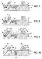
- FIG. 1illustrates a p-type field effect transistor (PFET) and an n-type field effect transistor (NFET) according to an embodiment of the invention.
- the PFET 10 and NFET 12are fabricated in a single-crystal semiconductor region 14 of a substrate 16 , separated by a trench isolation region 17 , typically of oxide.
- the substrate 16may either be a bulk substrate or may preferably be a semiconductor-on-insulator or silicon-on-insulator (SOI) substrate in which a relatively thin layer of a semiconductor is formed over an insulating layer 18 .
- SOIsilicon-on-insulator
- the substrateis preferably a bulk single-crystal silicon substrate, and more preferably a silicon SOI substrate having a single-crystal silicon region above an insulating layer.
- III-V compound semiconductorse.g. gallium arsenide (GaAs).
- the PFET 10includes a channel region 20 disposed below a polysilicon portion 26 of a gate conductor.
- the polysilicon portion 26is preferably heavily doped to a concentration of about 10 19 cm ⁇ 3 .
- the polysilicon portion 26includes a p-type dopant such as boron for the purpose of matching the workfunction of the p-type conduction channel that exists when the PFET is turned on in operation.
- the gate conductorpreferably also includes a low-resistance portion 28 disposed above the polysilicon portion 28 .
- the low-resistance portion 28has much less resistance than the polysilicon portion 26 , and preferably includes a metal, a silicide of a metal, or both.
- the low-resistance portion 28includes a silicide such as a silicide of cobalt (CoSi 2 ).
- a pair of silicided raised source-drain regions 11are disposed in single-crystal semiconductor regions on sides of the gate conductor 26 .
- Each of the raised source-drain regions 11is displaced from the gate conductor 26 by a pair of spacers 29 , 30 .
- Spacers 29 and 30are both preferably formed of silicon nitride, although spacer 30 can be formed of silicon dioxide instead or a combination of layers of silicon nitride and silicon dioxide, e.g. silicon oxynitride.
- a first strainis applied to the channel region 20 via a buried single-crystal layer 21 of a second semiconductor disposed under the source-drain regions 11 of the PFET 10 .
- the second semiconductor 21is preferably a lattice-mismatched semiconductor incorporating silicon and one or more other group IV elements such as carbon (C) or germanium (Ge).
- the second semiconductor layer 21is most preferably silicon germanium.
- a low resistance contact layer 24preferably being a silicide, is disposed above the first semiconductor layer 22 .
- the low-resistance layeris preferably a silicide, and more preferably a silicide of cobalt, i.e. CoSi 2 .
- the presence of a lattice-mismatched second semiconductor on sides of the channel region of the PFET 10produces a strain in the channel region 20 .
- the strainis compressive.
- Such compressive straincan range from a value as low as 50 MPa (megapascals) to several GPa (gigapascals).
- the strainproduces a positive effect upon mobility of charge carriers within the channel region 20 , which can measure up to several times the mobility of a PFET channel region which does not have such strain applied thereto.
- the lattice-mismatched second semiconductoris preferably a different semiconductor such as silicon germanium or silicon carbide, and more preferably silicon germanium (Si x Ge y ) where x and y are percentages where x plus y equals 100 percent.
- the ranges of variation between x and ycan be rather large, y illustratively varying from 1% to 99%, and in such case, x consequently varying between 99% and 1%.
- an NFET 12is provided in the single-crystal region 14 of the substrate.
- the NFET 12includes a channel region 40 disposed under a heavily doped n-type polysilicon portion 42 of a gate conductor which, in turn, is disposed under a low-resistance portion 44 of the NFET 12 .
- the low-resistance portion 44like the low-resistance portion 28 of the PFET 10 , can include a metal, a silicide, or both, and most preferably includes a silicide of cobalt (CoSi 2 ).
- the NFET 12also includes a pair of low-resistance raised source-drain contact regions 46 , each preferably including a low-resistance material such as a silicide, most preferably a silicide of cobalt (CoSi 2 ).
- each of the raised source-drain contact regions 46are spaced from the gate conductor portions 42 , 44 by a pair of spacers 47 , 48 .
- Spacer 47preferably includes silicon nitride
- spacer 48preferably includes silicon nitride, silicon dioxide or a combination of silicon nitride and silicon dioxide.
- the NFET 12does not have a first strain applied to the channel region 40 thereof, i.e. strain of the type and magnitude of the strain that is applied to the channel region 20 of the PFET 10 .
- the NFET 12has an n-type conduction channel having electrons as the dominant carrier.
- the NFET 12has a faster switching speed than a PFET 10 , when all other things are equal, because a PFET has a p-type conduction channel having holes rather than electrons as the dominant carrier. Holes have less mobility than electrons, hence the faster switching speed in the NFET 12 .
- the switching speed of the PFET 10must be increased to at least match that of NFET 12 .
- FIG. 2is a diagram illustrating a strain profile of a PFET 110 within a single-crystal region 114 of a substrate.
- the PFET 110has a structure as described above for PFET 10 , having a channel region 120 and raised source-drain regions on each side of the gate conductor, of which one raised source-drain region 111 is shown.
- the raised source-drain region 111includes a silicide region 124 disposed over a layer of silicon 122 , which in turn is disposed over a relatively thin layer 121 of a lattice-mismatched second semiconductor such as silicon germanium.
- the thin layer 121is disposed within a single-crystal region 114 of the substrate.
- the curved lines within the substrate 114indicate locations where a strain of the same magnitude and type (i.e. whether compressive or tensile) is present.
- line 126indicates locations of an equal strain applied to the channel region 120 .
- a compressive strain ranging between 50 MPa and 2 GPais preferably applied at such locations of the channel region 120 of the PFET 110 . More preferably, a compressive strain between 100 MPa and 1 GPa is applied to the channel region 120 . Most preferably, a compressive strain ranging between 200 MPa and 600 MPa is applied thereto, such that 400 MPa is a desired target for the strain.
- the magnitude and direction of strainis very different from the strain in the channel region 120 .
- the straincan range from 1 to 5 GPa, with 2.5 GPa being an approximate amount achieved for a particular geometry and dimensions of the PFET to apply the desired strain to the channel region 120 .
- the silicon layer 122 overlying the SiGe layerhas a tensile strain applied thereto.
- the particular magnitudes of the strains in the source-drain region 111are not so important. Applying a strain of a desired magnitude and direction to the channel region 120 of the PFET is the actual goal. Such strain is applied to the PFET, and not to the NFET, by performing processing methods according to embodiments of the invention.
- FIG. 3illustrates a first stage of a CMOS fabrication process according to an embodiment of the invention.
- PFETp-type field effect transistor
- NFETn-type field effect transistor
- a first strainis applied to the channel region by a lattice-mismatched semiconductor layer.
- the first strainis not applied since the lattice-mismatched semiconductor layer is not in close proximity thereto. In such manner, an increase in carrier mobility of the PFET is achieved while still maintaining desirable performance in the NFET.
- FIG. 3illustrates a stage in processing to form a PFET and an NFET according to an embodiment of the invention.
- a PFET gate stack 25 and an NFET gate stack 45are formed overlying a single-crystal region of a substrate.
- the single-crystal region 14consists essentially of a first semiconductor material such as silicon.
- the PFET gate stack 25includes a gate dielectric 13 overlying the single-crystal region 14 , a pair of spacers 29 formed on sidewalls of the gate conductor layer 26 and an insulating cap 50 .
- the NFET gate stack 45includes a gate dielectric 13 overlying the single-crystal region 14 , a pair of spacers 47 formed on sidewalls of the gate conductor layer 42 and an insulating cap 52 , also preferably formed by deposition of an oxide from a precursor of tetra-ethylorthosilicate (TEOS).
- TEOStetra-ethylorthosilicate
- the gate conductor layers 26 , 42preferably include only a heavily doped semiconductor, most preferably being a heavily doped polysilicon at this stage of processing.
- the gate conductors 26 , 42 of the respective PFET gate stack and NFET gate stackare already provided at this stage with desired dopant types and concentrations to provide desirable workfunctions.
- the PFET gate stackmay be provided with a p+ doped gate conductor layer 26 while the NFET gate stack may be provided with an n+ doped gate conductor layer 42 .
- the spacers 29are preferably formed of a deposited nitride and the insulating caps 50 , 52 are preferably formed by deposition of an oxide from a precursor of tetra-ethylorthosilicate (TEOS).
- a coating 56is applied to the main surface 54 of the single-crystal region 14 of the substrate.
- the coating 56is desirably applied by depositing a removable material which can limit the deposition of silicon in a selective deposition process.
- the materialis silicon nitride, and the material is preferably applied by deposition.
- a masking material 58is applied to the substrate and patterned to cover areas of the single-crystal region 14 on sides of the NFET gate stack 45 but not areas of the single-crystal region 14 on sides of the PFET gate stack 25 .
- the masking materialis preferably a photoresist.
- the masking materialcan be any one of several well-known etch-resistant materials which can later be completely removed such as antireflective coating (ARC), spin-on-glass, oxide from a TEOS precursor, or various doped glasses such as borosilicate glass (BSG), arsenic doped glass (ASG), phosphosilicate glass (PSG) or borophosphosilicate glass (BPSG) which can be deposited and thereafter removed.
- ARCantireflective coating
- SSGarsenic doped glass
- PSGphosphosilicate glass
- BPSGborophosphosilicate glass
- the single-crystal region 14is etched on sides of the PFET gate stack 25 , preferably by an anisotropic vertical etch process such as a reactive ion etch (RIE).
- RIEreactive ion etch
- the PFET gate stack 25provides a mask, preventing areas below the PFET gate stack 25 from being etched. Areas of the single-crystal region 14 on sides of the NFET gate stack 45 are not etched because they are protected by the masking layer 58 and the coating 56 .
- trenches 60are formed in the single-crystal region 14 on both sides of the PFET gate stack 25 .
- the masking layer 58is removed, as by a timed isotropic etch. This also has the effect of removing portions of the single-crystal silicon within the trenches 60 that may have become damaged as a result of the RIE etch.
- a layer 62 of a second semiconductoris grown epitaxially on the first semiconductor of the single-crystal region 14 in the trenches 60 .
- the epitaxial growth processis preferably performed by selective deposition such that very little material or none of the second semiconductor is deposited on surfaces other than as grown on the single-crystal semiconductor within the trenches 60 .
- the second semiconductoris a lattice-mismatched semiconductor capable of creating a strain as a layer grown in contact with a single-crystal region of another semiconductor.
- the epitaxially grown second semiconductor layer 62is recessed to a desirable level 64 below the main surface 54 of the single-crystal region of the substrate 14 .
- This recessing stepis preferably performed by a timed anisotropic reactive ion etch.
- the recessing stepcan be performed by an isotropic etch, selective to silicon, such that the etch proceeds faster against the exposed silicon germanium while etching the underlying silicon single-crystal region comparatively less.
- a second layer 66 of single-crystal siliconis epitaxially grown over the recessed layer 62 of silicon germanium.
- the second layer 66is preferably grown in a selective epitaxial deposition, such that comparatively little or no silicon is deposited except on the exposed areas of the silicon germanium layer 62 and exposed areas of the single-crystal silicon along the sidewalls of the trenches 60 .
- comparatively little or no siliconis deposited on the coating 56 and the PFET gate stack 25 .
- the coating 56is removed from the single-crystal region 14 on sides of the NFET gate stack 45 .
- a second pair of spacers 30are formed on sides of the PFET gate stack 25 and the NFET gate stack 45 .
- the spacers 30are preferably formed by conformally depositing an oxide material such as from a TEOS precursor followed by an anisotropic vertical etch such as RIE. The etch is preferably performed selective to silicon so as to avoid overly recessing the top layer of silicon 66 .
- the insulating caps 50are removed from the PFET gate stack 25 and the NFET gate stack 45 , exposing the polysilicon portions 26 and 42 below.
- a silicide 68is formed on the exposed semiconductor layer 66 , and the exposed single-crystal region on sides of the NFET gate stack 45 .
- a silicideis formed on the exposed polysilicon portions 26 , 42 of the PFET gate stack and the NFET gate stack, respectively.
- the silicideis preferably a silicide of cobalt (CoSi 2 ) which is preferably formed in a self-aligned manner (i.e., a “salicide”) by depositing a layer of cobalt over the processed substrate. Then, annealing is performed to react the cobalt with the silicon in contact therewith to form the silicide 68 . The unreacted cobalt is then removed from remaining areas of the processed substrate; that is, the spacers 29 , 30 and the trench isolation 17 .
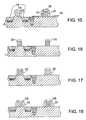
- FIGS. 10-14illustrate stages in fabrication of a chip having a strained channel region PFET and an NFET according to another method embodiment.
- FIG. 10illustrates a stage in processing, after the formation of a PFET gate stack 125 and an NFET gate stack 145 .
- These gate stackshave the same structure as described above with reference to FIG. 3 .
- PFET gate stackhas a gate conductor 126 overlying a gate dielectric 113 , nitride sidewall spacers 129 and oxide insulating cap 150 .
- the NFET gate stack 145has the same structure.
- a trench isolation 117lies between areas of the single-crystal region 114 of the substrate over which the PFET gate stack 125 and the NFET gate stack 145 are disposed.
- FIG. 10shows a stage in processing similar to that shown in FIG. 5 .
- a conformal masking layer 156has been deposited over the PFET gate stack 125 and the NFET gate stack 145 .
- the conformal masking layer 156preferably comprises an oxide such as silicon dioxide.
- Layer 156is removed from the area of the single-crystal region 114 surrounding the PFET gate stack 125 . This can be done in the same manner as that described above relative to FIG. 5 , by block masking the single-crystal region 114 surrounding the NFET gate stack 145 and thereafter vertically etching the layer 156 and the underlying areas 160 of the single-crystal region using an anisotropic etch such as RIE. During this etch the areas 160 are not etched as deeply as they are in the above-described embodiment. Rather, the areas 160 are etched only partially. Later, this etch will define the level at which a top layer of silicon will be formed.
- RIEanisotropic etch
- a second conformal masking layer 170is deposited to form the structure as shown.
- This layer 170is preferably silicon nitride as a conformal masking layer 170 that is capable of providing a stop against a subsequent step of selectively growing the lattice-mismatched semiconductor.
- an anisotropic vertical etch processsuch as RIE is performed to remove the masking layer 170 from the bottoms of the trenches 160 .
- spacers 172remain on sidewalls of the trenches 160 and gate stacks 125 , 145 .
- the masking layer 170is removed from all horizontal surfaces such as from insulating caps 150 and from over the first masking layer 156 in areas of the single-crystal region 114 surrounding the NFET gate stack 145 .
- the trenches 160are further recessed, as by an anisotropic vertical RIE selective to the material of the masking layer 170 , resulting in the structure as shown in FIG. 12 .
- the etchis performed selective to silicon nitride.
- this stepcan be performed by an isotropic etch selective to silicon nitride.
- a lattice-mismatched semiconductoris selectively grown in the trenches 160 .
- the lattice-mismatched semiconductoris preferably silicon germanium.
- a layer 176 of silicon germaniumis epitaxially grown on the bottom and sidewalls of the trenches 160 up to the level of the spacers 172 but not deposited elsewhere.
- the masking layer 170 and spacers 172are removed as by an isotropic wet strip process selective to silicon and the silicon germanium material in the trenches 160 .
- the single-crystal region 114 along the sidewalls 174 of the trenchesis exposed.
- a stepis performed to selectively grow an epitaxial layer 178 of silicon in the trenches 160 over the silicon germanium layer 176 .
- This results in the structure as shown in FIG. 15which is similar to that shown above in FIG. 8 with the exception that an oxide masking layer 156 remains over the NFET gate stack 145 in place of the nitride masking layer 56 in FIG. 8 .
- the oxide masking material 156can be removed, using a RIE etch. By this etch, the oxide insulating caps 150 are removed while leaving the nitride sidewall spacers 129 in place.
- the source and drain areas over the former trenches 160 and the tops of the polysilicon gate conductor layers 126 and 142can then be salicided, preferably by cobalt silicide, as described above relative to FIG. 9 .
- FIGS. 16 through 18illustrate an alternative embodiment to that described above relative to FIG. 9 .
- This alternative embodimentproceeds from a stage of processing such as that shown in FIG. 8 or FIG. 15 .
- the oxide masking layer 156 and the spacers 29 (or 129 )are removed from the polysilicon gate conductors 26 , 42 (or 126 , 142 ) and new spacers are provided in their place.
- the purpose of thisis to avoid device parameter shift brought about by changes in the characteristics of the spacers (e.g. incorporation of species) due to the increased thermal budget of the silicon germanium and silicon epitaxial growth processes.
- first spacers 230are formed on the polysilicon gate conductors 226 , 242 . This is preferably performed by conformally depositing silicon nitride and thereafter vertically etching, as by RIE. Then, extension and halo implants are performed into the source and drain regions of the PFET (i.e. into the areas of the single-crystal region 114 to the sides of spacers 230 of the PFET gate stack). Extension and halo implants are also performed into the source and drain regions of the NFET (i.e. into the areas of the single-crystal region 114 to the sides of spacers 230 of the NFET gate stack). Extension and halo implants are performed with only a first spacer 230 in place in order to implant to regions closer to the channel region of the PFET and NFET transistors in each case.
- second spacers 232are formed on the spacers 230 and then source and drain implants are performed on sides of the PFET gate stack to form PFET source and drain regions; and source and drain implants are performed on sides of the NFET gate stack to form NFET source and drain regions. In this way, the source and drain implanted regions are spaced a desirable distance from the channel regions of the transistors.
- a salicidecan be formed, in a manner such as that described above in the source and drain regions and over the polysilicon portions 226 and 242 of the PFET gate stack and the NFET gate stack, respectively.
- the foregoinghas described ways of fabricating a PFET and an NFET of an integrated circuit such that a first strain is applied to the channel region of the PFET via a lattice-mismatched semiconductor layer disposed in source and drain regions of the PFET.
- the first strainis not applied to the channel region of the NFET by virtue that the lattice-mismatched semiconductor layer is only disposed in the source and drain regions of the PFET and not in the source and drain regions of the NFET.
- a process of making the PFET and NFEThas been described such that a lattice-mismatched semiconductor is disposed in source and drain regions of only the PFET while not in the source and drain regions of the NFET.
- the processutilizing a masking layer formed over the NFET areas, relies on etching trenches in the areas to become the source and drain regions of the PFET, growing a silicon germanium layer epitaxially therein and then growing a silicon layer over the epitaxially grown silicon germanium layer.
Landscapes
- Metal-Oxide And Bipolar Metal-Oxide Semiconductor Integrated Circuits (AREA)
- Thin Film Transistor (AREA)
- Insulated Gate Type Field-Effect Transistor (AREA)
Abstract
Description
- This application is a divisional of commonly owned U.S. patent application Ser. No. 10/604,607 filed Aug. 8, 2003, the entire contents of which is hereby incorporated herein by reference.
- The present invention relates to the fabrication of semiconductor integrated circuits, and more specifically to an apparatus and method of making strained semiconductor complementary metal oxide semiconductor (CMOS) transistors having lattice-mismatched source and drain regions.
- Both theoretical and empirical studies have demonstrated that carrier mobility with a transistor is greatly increased when a strain is applied to the transistor's conduction channel. In p-type field effect transistors, the application of a compressive longitudinal strain to the conduction channel is known to increase the drive currents of the PFET. However, if that same strain is applied to the conduction channel of an NFET, its performance decreases.
- It has been proposed to apply a tensile longitudinal strain to the conduction channel of an NFET and apply a compressive longitudinal strain to the conduction channel of a PFET. Such proposals have focused on masked processes involving the masking of a PFET or NFET portion of the chip and altering the materials used in shallow trench isolation regions to apply the strain. The proposals have also included masked processes centered on modulating intrinsic stresses present in spacer features.
- Silicon germanium is a desirable lattice-mismatched semiconductor for use in forming strained silicon transistor channels. A strain is created when a first semiconductor is grown onto a single-crystal of a second semiconductor when the two semiconductors are lattice-mismatched to each other. Silicon and silicon germanium are lattice-mismatched to each other such that the growth of one of them onto the other produces a strain which can be either tensile or compressive.
- Silicon germanium grows epitaxially on silicon having a crystal structure aligned with the silicon crystal structure. However, because silicon germanium normally has a larger crystal structure than silicon, the epitaxially grown silicon germanium becomes internally compressed.
- In other proposals using strained silicon, silicon germanium forms a single-crystal layer of an entire substrate. In such case, the silicon germanium layer is known as a relaxed layer, because the strain is released by forming dislocations within the silicon germanium layer. When a single-crystal silicon layer is grown epitaxially on a relaxed SiGe crystal region, a tensile strain is produced in the epitaxially grown silicon crystal. This results in improved electron mobility, which is capable of improving the performance of an NFET. However, such technique requires the SiGe to be relaxed, which requires that the SiGe layer be very thick, i.e. 0.5 to 1.0 μm. Improvements in the mobility of holes is difficult to obtain because to do so, the SiGe layer requires a large percentage of germanium, which can result in excessive dislocations in the SiGe crystal, causing yield problems. Further, processing costs can be prohibitive.
- Other techniques such as graded Ge concentration and chemical mechanical polishing methods are used to improve the quality of the films. However, those techniques are plagued by high cost and high defect density.
- Accordingly, it would be desirable to create a strain in the channel region of a PFET without the use of a thick SiGe crystal region. It would be desirable create a desired strain in a channel region of a device using a relatively thin epitaxially grown SiGe.
- It would further be desirable to create a compressive strain to increase hole mobility in the channel region of a PFET by growing an epitaxial layer of SiGe in the source and drain regions of the PFET.
- It would further be desirable to provide a process for applying a desired strain in the channel region of a PFET without creating the same strain in the channel region of the NFET.
- According to an aspect of the invention, a p-type field effect transistor (PFET) and an n-type field effect transistor (NFET) of an integrated circuit are provided. A first strain is applied to the channel region of the PFET but not the NFET via a lattice-mismatched semiconductor layer such as silicon germanium disposed in source and drain regions of only the PFET and not of the NFET. A process of making the PFET and NFET is provided. Trenches are etched in the areas to become the source and drain regions of the PFET and a lattice-mismatched silicon germanium layer is grown epitaxially therein to apply a strain to the channel region of the PFET adjacent thereto.
- In an aspect of the invention, a layer of silicon can be grown over the silicon germanium layer and a salicide formed from the layer of silicon to provide low-resistance source and drain regions. Simultaneously, the salicide can be formed in the gate conductors of the PFET and NFET.
FIG. 1 illustrates a PFET and an NFET according to an embodiment of the invention.FIG. 2 illustrates a strain profile of a PFET according to an embodiment of the invention.FIGS. 3 through 9 illustrate stages in fabrication of a PFET and an NFET according to an embodiment of the invention.FIGS. 10 through 15 illustrate stages in fabrication of a PFET and an NFET according to another embodiment of the invention.FIGS. 16 through 18 illustrate stages in fabrication of a PFET and an NFET according to yet another embodiment of the invention.FIG. 1 illustrates a p-type field effect transistor (PFET) and an n-type field effect transistor (NFET) according to an embodiment of the invention. As illustrated inFIG. 1 , thePFET 10 and NFET12 are fabricated in a single-crystal semiconductor region 14 of asubstrate 16, separated by atrench isolation region 17, typically of oxide. Thesubstrate 16 may either be a bulk substrate or may preferably be a semiconductor-on-insulator or silicon-on-insulator (SOI) substrate in which a relatively thin layer of a semiconductor is formed over aninsulating layer 18. When field effect transistors (FETs) are formed in such SOI substrates, faster switching operation is often achieved than otherwise, because junction capacitance between the channel region of the transistor and the bulk substrate is eliminated. The substrate is preferably a bulk single-crystal silicon substrate, and more preferably a silicon SOI substrate having a single-crystal silicon region above an insulating layer. As described in this and the embodiments to follow, reference will be made to fabrication of transistors within a single-crystal silicon region of a substrate, as opposed to other types of semiconductors such as III-V compound semiconductors, e.g. gallium arsenide (GaAs).- As shown in
FIG. 1 , thePFET 10 includes achannel region 20 disposed below apolysilicon portion 26 of a gate conductor. Thepolysilicon portion 26 is preferably heavily doped to a concentration of about 1019cm−3. Preferably thepolysilicon portion 26 includes a p-type dopant such as boron for the purpose of matching the workfunction of the p-type conduction channel that exists when the PFET is turned on in operation. The gate conductor preferably also includes a low-resistance portion 28 disposed above thepolysilicon portion 28. The low-resistance portion 28 has much less resistance than thepolysilicon portion 26, and preferably includes a metal, a silicide of a metal, or both. In a preferred embodiment, the low-resistance portion 28 includes a silicide such as a silicide of cobalt (CoSi2). - A pair of silicided raised source-
drain regions 11 are disposed in single-crystal semiconductor regions on sides of thegate conductor 26. Each of the raised source-drain regions 11 is displaced from thegate conductor 26 by a pair ofspacers Spacers spacer 30 can be formed of silicon dioxide instead or a combination of layers of silicon nitride and silicon dioxide, e.g. silicon oxynitride. - A first strain is applied to the
channel region 20 via a buried single-crystal layer 21 of a second semiconductor disposed under the source-drain regions 11 of thePFET 10. Thesecond semiconductor 21 is preferably a lattice-mismatched semiconductor incorporating silicon and one or more other group IV elements such as carbon (C) or germanium (Ge). Thesecond semiconductor layer 21 is most preferably silicon germanium. Alayer 22 of the first semiconductor, preferably being silicon, is disposed above thesecond semiconductor layer 21. Preferably, a lowresistance contact layer 24, preferably being a silicide, is disposed above thefirst semiconductor layer 22. The low-resistance layer is preferably a silicide, and more preferably a silicide of cobalt, i.e. CoSi2. - The presence of a lattice-mismatched second semiconductor on sides of the channel region of the
PFET 10 produces a strain in thechannel region 20. Preferably, the strain is compressive. Such compressive strain can range from a value as low as 50 MPa (megapascals) to several GPa (gigapascals). The strain produces a positive effect upon mobility of charge carriers within thechannel region 20, which can measure up to several times the mobility of a PFET channel region which does not have such strain applied thereto. - As the first semiconductor is preferably silicon, the lattice-mismatched second semiconductor is preferably a different semiconductor such as silicon germanium or silicon carbide, and more preferably silicon germanium (SixGey) where x and y are percentages where x plus y equals 100 percent. The ranges of variation between x and y can be rather large, y illustratively varying from 1% to 99%, and in such case, x consequently varying between 99% and 1%.
- Alternatively, the single crystal region of the
substrate 14 may consist essentially of silicon germanium in proportions according to a first formula Six1Gey1, where x1 and y1 are percentages where x1+y1=100%, and the layer of the second semiconductor consists essentially of silicon germanium in different proportions according to a second formula Six2Gey2, where x1 and y1 are percentages where x2+y2=100%, x1 not equal to x2, y1 not equal to y2. - As also illustrated in
FIG. 1 , anNFET 12 is provided in the single-crystal region 14 of the substrate. TheNFET 12 includes achannel region 40 disposed under a heavily doped n-type polysilicon portion 42 of a gate conductor which, in turn, is disposed under a low-resistance portion 44 of theNFET 12. The low-resistance portion 44, like the low-resistance portion 28 of thePFET 10, can include a metal, a silicide, or both, and most preferably includes a silicide of cobalt (CoSi2). - The
NFET 12 also includes a pair of low-resistance raised source-drain contact regions 46, each preferably including a low-resistance material such as a silicide, most preferably a silicide of cobalt (CoSi2). Preferably, each of the raised source-drain contact regions 46 are spaced from thegate conductor portions spacers Spacer 47 preferably includes silicon nitride, andspacer 48 preferably includes silicon nitride, silicon dioxide or a combination of silicon nitride and silicon dioxide. NFET 12 does not have a first strain applied to thechannel region 40 thereof, i.e. strain of the type and magnitude of the strain that is applied to thechannel region 20 of thePFET 10. This is because of the following reasons. First, theNFET 12 has an n-type conduction channel having electrons as the dominant carrier. TheNFET 12 has a faster switching speed than aPFET 10, when all other things are equal, because a PFET has a p-type conduction channel having holes rather than electrons as the dominant carrier. Holes have less mobility than electrons, hence the faster switching speed in theNFET 12. Thus, the switching speed of thePFET 10 must be increased to at least match that ofNFET 12.- Secondly, the same type of and magnitude of strain cannot be applied to both
PFET 10 andNFET 12 because it would not have the same effect onNFET 12. A high magnitude compressive strain (e.g 50 MPa to several GPa) applied to thechannel region 40 of theNFET 12 would actually reduce the mobility of the electrons therein, leading to a slower, rather than faster switching speed as desired. FIG. 2 is a diagram illustrating a strain profile of aPFET 110 within a single-crystal region 114 of a substrate. ThePFET 110 has a structure as described above forPFET 10, having achannel region 120 and raised source-drain regions on each side of the gate conductor, of which one raised source-drain region 111 is shown. The raised source-drain region 111 includes a silicide region124 disposed over a layer of silicon122, which in turn is disposed over a relativelythin layer 121 of a lattice-mismatched second semiconductor such as silicon germanium. Thethin layer 121, in turn, is disposed within a single-crystal region 114 of the substrate.- In
FIG. 2 , the curved lines within thesubstrate 114 indicate locations where a strain of the same magnitude and type (i.e. whether compressive or tensile) is present. Thus,line 126 indicates locations of an equal strain applied to thechannel region 120. A compressive strain ranging between 50 MPa and 2 GPa is preferably applied at such locations of thechannel region 120 of thePFET 110. More preferably, a compressive strain between 100 MPa and 1 GPa is applied to thechannel region 120. Most preferably, a compressive strain ranging between 200 MPa and 600 MPa is applied thereto, such that 400 MPa is a desired target for the strain. In the source-drain region 111, the magnitude and direction of strain is very different from the strain in thechannel region 120. In the buriedSiGe layer 121, the strain can range from 1 to 5 GPa, with 2.5 GPa being an approximate amount achieved for a particular geometry and dimensions of the PFET to apply the desired strain to thechannel region 120. On the other hand, the silicon layer122 overlying the SiGe layer has a tensile strain applied thereto. The particular magnitudes of the strains in the source-drain region 111 are not so important. Applying a strain of a desired magnitude and direction to thechannel region 120 of the PFET is the actual goal. Such strain is applied to the PFET, and not to the NFET, by performing processing methods according to embodiments of the invention. FIG. 3 illustrates a first stage of a CMOS fabrication process according to an embodiment of the invention. As a result of processing according to the embodiment, a p-type field effect transistor (PFET) and an n-type field effect transistor (NFET) are formed. In the PFET, a first strain is applied to the channel region by a lattice-mismatched semiconductor layer. On the other hand, in the channel region of the NFET, the first strain is not applied since the lattice-mismatched semiconductor layer is not in close proximity thereto. In such manner, an increase in carrier mobility of the PFET is achieved while still maintaining desirable performance in the NFET.FIG. 3 illustrates a stage in processing to form a PFET and an NFET according to an embodiment of the invention. As shown inFIG. 3 , aPFET gate stack 25 and anNFET gate stack 45 are formed overlying a single-crystal region of a substrate. The single-crystal region 14 consists essentially of a first semiconductor material such as silicon. ThePFET gate stack 25 includes agate dielectric 13 overlying the single-crystal region 14, a pair ofspacers 29 formed on sidewalls of thegate conductor layer 26 and an insulatingcap 50. TheNFET gate stack 45 includes agate dielectric 13 overlying the single-crystal region 14, a pair ofspacers 47 formed on sidewalls of thegate conductor layer 42 and an insulatingcap 52, also preferably formed by deposition of an oxide from a precursor of tetra-ethylorthosilicate (TEOS).- The gate conductor layers26,42 preferably include only a heavily doped semiconductor, most preferably being a heavily doped polysilicon at this stage of processing. Preferably, the
gate conductors gate conductor layer 26 while the NFET gate stack may be provided with an n+ dopedgate conductor layer 42. Thespacers 29 are preferably formed of a deposited nitride and the insulatingcaps - Next, as shown in
FIG. 4 , acoating 56 is applied to themain surface 54 of the single-crystal region 14 of the substrate. Thecoating 56 is desirably applied by depositing a removable material which can limit the deposition of silicon in a selective deposition process. Preferably, the material is silicon nitride, and the material is preferably applied by deposition. Next, as shown inFIG. 5 , a maskingmaterial 58 is applied to the substrate and patterned to cover areas of the single-crystal region 14 on sides of theNFET gate stack 45 but not areas of the single-crystal region 14 on sides of thePFET gate stack 25. In an embodiment, the masking material is preferably a photoresist. Alternatively, the masking material can be any one of several well-known etch-resistant materials which can later be completely removed such as antireflective coating (ARC), spin-on-glass, oxide from a TEOS precursor, or various doped glasses such as borosilicate glass (BSG), arsenic doped glass (ASG), phosphosilicate glass (PSG) or borophosphosilicate glass (BPSG) which can be deposited and thereafter removed. - Thereafter, the single-
crystal region 14 is etched on sides of thePFET gate stack 25, preferably by an anisotropic vertical etch process such as a reactive ion etch (RIE). During such etch, thePFET gate stack 25 provides a mask, preventing areas below the PFET gate stack25 from being etched. Areas of the single-crystal region 14 on sides of theNFET gate stack 45 are not etched because they are protected by themasking layer 58 and thecoating 56. As a result of the etching,trenches 60 are formed in the single-crystal region 14 on both sides of thePFET gate stack 25. After etching thetrenches 60, themasking layer 58 is removed, as by a timed isotropic etch. This also has the effect of removing portions of the single-crystal silicon within thetrenches 60 that may have become damaged as a result of the RIE etch. - Thereafter, as shown in
FIG. 6 , alayer 62 of a second semiconductor is grown epitaxially on the first semiconductor of the single-crystal region 14 in thetrenches 60. The epitaxial growth process is preferably performed by selective deposition such that very little material or none of the second semiconductor is deposited on surfaces other than as grown on the single-crystal semiconductor within thetrenches 60. The second semiconductor is a lattice-mismatched semiconductor capable of creating a strain as a layer grown in contact with a single-crystal region of another semiconductor. - Next, as shown in
FIG. 7 , with thecoating 56 still in place to protect the areas in which the NFET will be formed, the epitaxially grownsecond semiconductor layer 62 is recessed to adesirable level 64 below themain surface 54 of the single-crystal region of thesubstrate 14. This recessing step is preferably performed by a timed anisotropic reactive ion etch. Alternatively, the recessing step can be performed by an isotropic etch, selective to silicon, such that the etch proceeds faster against the exposed silicon germanium while etching the underlying silicon single-crystal region comparatively less. - Next, as shown in
FIG. 8 , asecond layer 66 of single-crystal silicon is epitaxially grown over the recessedlayer 62 of silicon germanium. Thesecond layer 66 is preferably grown in a selective epitaxial deposition, such that comparatively little or no silicon is deposited except on the exposed areas of thesilicon germanium layer 62 and exposed areas of the single-crystal silicon along the sidewalls of thetrenches 60. Thus, as a result of the selective epitaxial deposition, comparatively little or no silicon is deposited on thecoating 56 and thePFET gate stack 25. - Next, as shown in
FIG. 9 , thecoating 56 is removed from the single-crystal region 14 on sides of theNFET gate stack 45. Next, a second pair ofspacers 30, preferably including an oxide material, are formed on sides of thePFET gate stack 25 and theNFET gate stack 45. Thespacers 30 are preferably formed by conformally depositing an oxide material such as from a TEOS precursor followed by an anisotropic vertical etch such as RIE. The etch is preferably performed selective to silicon so as to avoid overly recessing the top layer ofsilicon 66. As a result of this etch step, the insulatingcaps 50 are removed from thePFET gate stack 25 and theNFET gate stack 45, exposing thepolysilicon portions - Thereafter, as shown in
FIG. 9 , asilicide 68 is formed on the exposedsemiconductor layer 66, and the exposed single-crystal region on sides of theNFET gate stack 45. At the same time, a silicide is formed on the exposedpolysilicon portions silicide 68. The unreacted cobalt is then removed from remaining areas of the processed substrate; that is, thespacers trench isolation 17. FIGS. 10-14 illustrate stages in fabrication of a chip having a strained channel region PFET and an NFET according to another method embodiment.FIG. 10 illustrates a stage in processing, after the formation of aPFET gate stack 125 and an NFET gate stack145. These gate stacks have the same structure as described above with reference toFIG. 3 . For example, PFET gate stack has agate conductor 126 overlying agate dielectric 113,nitride sidewall spacers 129 andoxide insulating cap 150. The NFET gate stack145 has the same structure. Atrench isolation 117 lies between areas of the single-crystal region 114 of the substrate over which thePFET gate stack 125 and the NFET gate stack145 are disposed.FIG. 10 shows a stage in processing similar to that shown inFIG. 5 . Aconformal masking layer 156 has been deposited over thePFET gate stack 125 and the NFET gate stack145. Theconformal masking layer 156 preferably comprises an oxide such as silicon dioxide.Layer 156 is removed from the area of the single-crystal region 114 surrounding thePFET gate stack 125. This can be done in the same manner as that described above relative toFIG. 5 , by block masking the single-crystal region 114 surrounding the NFET gate stack145 and thereafter vertically etching thelayer 156 and theunderlying areas 160 of the single-crystal region using an anisotropic etch such as RIE. During this etch theareas 160 are not etched as deeply as they are in the above-described embodiment. Rather, theareas 160 are etched only partially. Later, this etch will define the level at which a top layer of silicon will be formed.- Next, a second
conformal masking layer 170 is deposited to form the structure as shown. Thislayer 170 is preferably silicon nitride as aconformal masking layer 170 that is capable of providing a stop against a subsequent step of selectively growing the lattice-mismatched semiconductor. Next, as shown inFIG. 11 , an anisotropic vertical etch process such as RIE is performed to remove themasking layer 170 from the bottoms of thetrenches 160. During this process,spacers 172 remain on sidewalls of thetrenches 160 andgate stacks 125,145. During the etch, themasking layer 170 is removed from all horizontal surfaces such as from insulatingcaps 150 and from over thefirst masking layer 156 in areas of the single-crystal region 114 surrounding the NFET gate stack145. - After this etch, the
trenches 160 are further recessed, as by an anisotropic vertical RIE selective to the material of themasking layer 170, resulting in the structure as shown inFIG. 12 . For example, if themasking layer 170 includes silicon nitride, then the etch is performed selective to silicon nitride. Alternatively, this step can be performed by an isotropic etch selective to silicon nitride. - Next, as illustrated in
FIG. 13 , a lattice-mismatched semiconductor is selectively grown in thetrenches 160. The lattice-mismatched semiconductor is preferably silicon germanium. By this process, alayer 176 of silicon germanium is epitaxially grown on the bottom and sidewalls of thetrenches 160 up to the level of thespacers 172 but not deposited elsewhere. - Thereafter, as shown in
FIG. 14 , themasking layer 170 andspacers 172 are removed as by an isotropic wet strip process selective to silicon and the silicon germanium material in thetrenches 160. As a result, the single-crystal region 114 along thesidewalls 174 of the trenches is exposed. - Next, a step is performed to selectively grow an
epitaxial layer 178 of silicon in thetrenches 160 over thesilicon germanium layer 176. This results in the structure as shown inFIG. 15 , which is similar to that shown above inFIG. 8 with the exception that anoxide masking layer 156 remains over the NFET gate stack145 in place of thenitride masking layer 56 inFIG. 8 . - Thereafter, the
oxide masking material 156 can be removed, using a RIE etch. By this etch, theoxide insulating caps 150 are removed while leaving thenitride sidewall spacers 129 in place. The source and drain areas over theformer trenches 160 and the tops of the polysilicon gate conductor layers126 and142 can then be salicided, preferably by cobalt silicide, as described above relative toFIG. 9 . FIGS. 16 through 18 illustrate an alternative embodiment to that described above relative toFIG. 9 . This alternative embodiment proceeds from a stage of processing such as that shown inFIG. 8 orFIG. 15 . As shown inFIG. 16 , in this embodiment, theoxide masking layer 156 and the spacers29 (or129) are removed from thepolysilicon gate conductors 26,42 (or126,142) and new spacers are provided in their place. The purpose of this is to avoid device parameter shift brought about by changes in the characteristics of the spacers (e.g. incorporation of species) due to the increased thermal budget of the silicon germanium and silicon epitaxial growth processes.- As shown in
FIG. 17 ,first spacers 230 are formed on thepolysilicon gate conductors crystal region 114 to the sides ofspacers 230 of the PFET gate stack). Extension and halo implants are also performed into the source and drain regions of the NFET (i.e. into the areas of the single-crystal region 114 to the sides ofspacers 230 of the NFET gate stack). Extension and halo implants are performed with only afirst spacer 230 in place in order to implant to regions closer to the channel region of the PFET and NFET transistors in each case. - Thereafter,
second spacers 232 are formed on thespacers 230 and then source and drain implants are performed on sides of the PFET gate stack to form PFET source and drain regions; and source and drain implants are performed on sides of the NFET gate stack to form NFET source and drain regions. In this way, the source and drain implanted regions are spaced a desirable distance from the channel regions of the transistors. - Thereafter, a salicide can be formed, in a manner such as that described above in the source and drain regions and over the
polysilicon portions - The foregoing has described ways of fabricating a PFET and an NFET of an integrated circuit such that a first strain is applied to the channel region of the PFET via a lattice-mismatched semiconductor layer disposed in source and drain regions of the PFET. The first strain is not applied to the channel region of the NFET by virtue that the lattice-mismatched semiconductor layer is only disposed in the source and drain regions of the PFET and not in the source and drain regions of the NFET.
- A process of making the PFET and NFET has been described such that a lattice-mismatched semiconductor is disposed in source and drain regions of only the PFET while not in the source and drain regions of the NFET. The process, utilizing a masking layer formed over the NFET areas, relies on etching trenches in the areas to become the source and drain regions of the PFET, growing a silicon germanium layer epitaxially therein and then growing a silicon layer over the epitaxially grown silicon germanium layer.
- While the invention has been described with reference to certain preferred embodiments thereof, those skilled in the art will understand the many modifications and enhancements which can be made without departing from the true scope and spirit of the invention, which is limited only by the appended claims.
Claims (20)
1. A method of fabricating a p-type field effect transistor (PFET) and an n-type field effect transistor (NFET), said NFET and said PFET each having a channel region, said channel region of said PFET having a first strain and said channel region of said NFET not having said first strain, said method comprising:
forming a PFET gate stack and an NFET gate stack over a main surface of a first semiconductor region having a first composition, each of said PFET gate stack and said NFET gate stack including a gate dielectric, a gate conductor overlying said gate dielectric, a cap layer overlying said gate conductor and first spacers disposed adjacent to sidewalls of said gate conductor;
recessing a portion of said first semiconductor region adjacent to said first spacers of said PFET gate stack while protecting another portion of said first semiconductor region adjacent to said first spacers of said NFET gate stack from being recessed;
growing a second semiconductor region overlying said recessed portion of said first semiconductor region while preventing said second semiconductor region from growing on said another portion of said first semiconductor region adjacent to said first spacers of said NFET gate stack, wherein said second semiconductor region has a second composition lattice-mismatched to a first composition of said first semiconductor region, such that said second semiconductor region applies a first strain to said channel region of said PFET; and
fabricating source regions and drain regions of said PFET adjacent to said PFET gate stack and fabricating source regions and drain regions of said NFET adjacent to said NFET gate stack.
2. The method ofclaim 1 further comprising recessing said second semiconductor region below said main surface of said first semiconductor region.
3. The method ofclaim 2 further comprising growing a semiconductor layer having said first composition over said recessed second semiconductor region.
4. The method ofclaim 3 further comprising forming a self-aligned silicide overlying said source regions and said drain regions of said PFET and overlying said source regions and said drain regions of said NFET.
5. The method ofclaim 4 further comprising forming a self-aligned silicide overlying polysilicon portions of said gate conductors of said PFET and said NFET.
6. The method ofclaim 5 wherein said silicide includes a silicide of cobalt.
7. The method ofclaim 3 wherein said first composition consists essentially of silicon and said second composition includes silicon germanium having a germanium content of at least one percent.
8. The method ofclaim 7 wherein said first strain is a compressive strain.
9. The method ofclaim 1 wherein said step of fabricating said source regions and said drain regions further includes removing said first spacers from said PFET gate stack and said NFET gate stack and forming second spacers on sidewalls of said PFET gate stack and said NFET gate stack.
10. The method ofclaim 9 wherein said second spacers have a greater thickness than said first spacers.
11. The method ofclaim 3 further comprising halo implanting said NFET and said PFET, wherein said halo implanting of said PFET includes implanting said semiconductor layer having said first composition.
12. The method ofclaim 3 further comprising extension implanting said NFET and said PFET, wherein said extension implanting of said PFET includes implanting said semiconductor layer having said first composition.
13. The method ofclaim 10 further comprising forming third spacers laterally contacting said second spacers, wherein said step of fabricating said source regions and said drain regions includes performing source and drain implants masked by said first spacers, said second spacers and said third spacers.
14. The method ofclaim 1 , wherein said first composition consists essentially of silicon germanium according to a first formula Six1Gey1, where x1 and y1 are percentages, x1+y1=100%, y1 being at least one percent and said second composition consists essentially of silicon germanium according to a second formula Six2Gey2, where x2 and y2 are percentages, x2+y2=100%, y2 being at least one percent, wherein x1 is not equal to x2 and y1 is not equal to y2.
15. A method of fabricating a p-type field effect transistor (PFET) and an n-type field effect transistor (NFET), said NFET and said PFET each having a channel region, said channel region of said PFET having a first strain and said channel region of said NFET not having said first strain, said method comprising:
forming a PFET gate stack and an NFET gate stack over a main surface of a first semiconductor region having a first composition, each of said PFET gate stack and said NFET gate stack including a gate dielectric, a gate conductor overlying said gate dielectric, a cap layer overlying said gate conductor and first spacers disposed adjacent to sidewalls of said gate conductor;
applying a thick mask to cover a portion of said first semiconductor region adjacent to said first spacers of said NFET gate stack and to expose another portion of said first semiconductor region adjacent to said first spacers of said PFET gate stack;
recessing said exposed portion of said first semiconductor region adjacent to said first spacers of said PFET gate stack;
removing said thick mask and forming a conformal coating substantially covering said portion of said first semiconductor region adjacent to said first spacers of said NFET gate stack and at least substantially exposing said recessed portion of said first semiconductor region adjacent to said first spacers of said PFET gate stack;
selectively growing a second semiconductor region overlying said recessed portion of said first semiconductor region, said conformal coating preventing said second semiconductor region from growing on said first semiconductor region adjacent to said first spacers of said NFET gate stack, wherein said second semiconductor region has a second composition lattice-mismatched to a first composition of said first semiconductor region, such that said second semiconductor region applies a first strain to said channel region of said PFET; and
fabricating source and drain regions of said PFET adjacent to said PFET gate stack and fabricating source and drain regions of said NFET adjacent to said NFET gate stack.
16. A method of fabricating a p-type field effect transistor (PFET) and an n-type field effect transistor (NFET), said NFET and said PFET each having a channel region, said channel region of said PFET having a first strain and said channel region of said NFET not having said first strain, said method comprising:
forming a PFET gate stack and an NFET gate stack over a main surface of a first semiconductor region having a first composition, each of said PFET gate stack and said NFET gate stack including a gate dielectric, a gate conductor overlying said gate dielectric, a cap layer overlying said gate conductor and first spacers disposed adjacent to sidewalls of said gate conductor;
applying a first mask to cover a portion of said first semiconductor region adjacent to said first spacers of said NFET gate stack and to expose another portion of said first semiconductor region adjacent to said first spacers of said PFET gate stack;
partially recessing said exposed portion of said first semiconductor region adjacent to said first spacers of said PFET gate stack;
removing said first mask and forming a first conformal coating substantially covering said portion of said first semiconductor region adjacent to said first spacers of said NFET gate stack and at least substantially exposing a bottom of said recessed portion of said first semiconductor region adjacent to said first spacers of said PFET;
forming an inner spacer covering an inner wall of said recessed portion of said first semiconductor region;
further recessing said partially recessed portion of said first semiconductor region;
selectively growing a second semiconductor region overlying said recessed portion of said first semiconductor region, wherein said first conformal coating prevents said second semiconductor region from growing on said first semiconductor region adjacent to said first spacers of said NFET gate stack, said inner spacer determines a location of said second semiconductor region, and said second semiconductor region has a second composition lattice-mismatched to a first composition of said first semiconductor region, such that said second semiconductor region applies a first strain to said channel region of said PFET; and
fabricating source and drain regions of said PFET adjacent to said PFET gate stack and fabricating source and drain regions of said NFET adjacent to said NFET gate stack.
17. The method ofclaim 16 , wherein said second semiconductor region has a top surface parallel to said main surface, wherein a depth of said inner spacer determines a depth of said top surface from said main surface
18. The method ofclaim 16 further comprising growing a semiconductor layer having said first composition over said second semiconductor region.
19. The method ofclaim 16 wherein said first composition consists essentially of silicon and said second composition includes silicon germanium, said silicon germanium having a germanium content of at least one percent.
20. The method ofclaim 16 , wherein said first composition consists essentially of silicon germanium according to a first formula Six1Gey1, where x1 and y1 are percentages, x1+y1=100%, y1 being at least one percent and said second composition consists essentially of silicon germanium according to a second formula Six2Gey2, where x2 and y2 are percentages, x2+y2=100%, y2 being at least one percent, wherein x1 is not equal to x2 and y1 is not equal to y2.
Priority Applications (2)
| Application Number | Priority Date | Filing Date | Title |
|---|---|---|---|
| US11/081,271US7291528B2 (en) | 2003-08-04 | 2005-03-16 | Method of making strained semiconductor transistors having lattice-mismatched semiconductor regions underlying source and drain regions |
| US11/820,303US7396714B2 (en) | 2003-08-04 | 2007-06-18 | Method of making strained semiconductor transistors having lattice-mismatched semiconductor regions underlying source and drain regions |
Applications Claiming Priority (2)
| Application Number | Priority Date | Filing Date | Title |
|---|---|---|---|
| US10/604,607US6891192B2 (en) | 2003-08-04 | 2003-08-04 | Structure and method of making strained semiconductor CMOS transistors having lattice-mismatched semiconductor regions underlying source and drain regions |
| US11/081,271US7291528B2 (en) | 2003-08-04 | 2005-03-16 | Method of making strained semiconductor transistors having lattice-mismatched semiconductor regions underlying source and drain regions |
Related Parent Applications (1)
| Application Number | Title | Priority Date | Filing Date |
|---|---|---|---|
| US10/604,607DivisionUS6891192B2 (en) | 2003-08-04 | 2003-08-04 | Structure and method of making strained semiconductor CMOS transistors having lattice-mismatched semiconductor regions underlying source and drain regions |
Related Child Applications (2)
| Application Number | Title | Priority Date | Filing Date |
|---|---|---|---|
| US11/820,303DivisionUS7396714B2 (en) | 2003-08-04 | 2007-06-18 | Method of making strained semiconductor transistors having lattice-mismatched semiconductor regions underlying source and drain regions |
| US11/820,303ContinuationUS7396714B2 (en) | 2003-08-04 | 2007-06-18 | Method of making strained semiconductor transistors having lattice-mismatched semiconductor regions underlying source and drain regions |
Publications (2)
| Publication Number | Publication Date |
|---|---|
| US20050158931A1true US20050158931A1 (en) | 2005-07-21 |
| US7291528B2 US7291528B2 (en) | 2007-11-06 |
Family
ID=34115654
Family Applications (3)
| Application Number | Title | Priority Date | Filing Date |
|---|---|---|---|
| US10/604,607Expired - LifetimeUS6891192B2 (en) | 2003-08-04 | 2003-08-04 | Structure and method of making strained semiconductor CMOS transistors having lattice-mismatched semiconductor regions underlying source and drain regions |
| US11/081,271Expired - Fee RelatedUS7291528B2 (en) | 2003-08-04 | 2005-03-16 | Method of making strained semiconductor transistors having lattice-mismatched semiconductor regions underlying source and drain regions |
| US11/820,303Expired - LifetimeUS7396714B2 (en) | 2003-08-04 | 2007-06-18 | Method of making strained semiconductor transistors having lattice-mismatched semiconductor regions underlying source and drain regions |
Family Applications Before (1)
| Application Number | Title | Priority Date | Filing Date |
|---|---|---|---|
| US10/604,607Expired - LifetimeUS6891192B2 (en) | 2003-08-04 | 2003-08-04 | Structure and method of making strained semiconductor CMOS transistors having lattice-mismatched semiconductor regions underlying source and drain regions |
Family Applications After (1)
| Application Number | Title | Priority Date | Filing Date |
|---|---|---|---|
| US11/820,303Expired - LifetimeUS7396714B2 (en) | 2003-08-04 | 2007-06-18 | Method of making strained semiconductor transistors having lattice-mismatched semiconductor regions underlying source and drain regions |
Country Status (10)
| Country | Link |
|---|---|
| US (3) | US6891192B2 (en) |
| EP (1) | EP1654770B1 (en) |
| JP (1) | JP4808618B2 (en) |
| KR (1) | KR100791441B1 (en) |
| CN (1) | CN100428497C (en) |
| AT (1) | ATE504078T1 (en) |
| DE (1) | DE602004032035D1 (en) |
| IL (1) | IL173422A (en) |
| TW (1) | TWI284961B (en) |
| WO (1) | WO2005017964A2 (en) |
Cited By (25)
| Publication number | Priority date | Publication date | Assignee | Title |
|---|---|---|---|---|
| US20070072376A1 (en)* | 2005-09-29 | 2007-03-29 | Semiconductor Manufacturing International (Shanghai) Corporation | Strained-induced mobility enhancement nano-device structure and integrated process architecture for CMOS technologies |
| US20070096201A1 (en)* | 2005-10-31 | 2007-05-03 | Semiconductor Manufacturing International (Shanghai) Corporation | Single mask scheme method and structure for integrating PMOS and NMOS transistors using strained silicon |
| EP1801864A1 (en)* | 2005-12-23 | 2007-06-27 | Inter-Universitair Microelektronica Centrum | Method for selective epitaxial growth of source/drain areas |
| US20070238233A1 (en)* | 2006-03-30 | 2007-10-11 | Sadaka Mariam G | Method of making a multiple crystal orientation semiconductor device |
| US20070262361A1 (en)* | 2005-01-18 | 2007-11-15 | International Business Machines Corporation | Structure and method for manufacturing strained silicon directly-on-insulator substrate with hybrid crystalline orientation and different stress levels |
| US20080023752A1 (en)* | 2006-07-28 | 2008-01-31 | International Business Machines Corporation | BORON DOPED SiGe HALO FOR NFET TO CONTROL SHORT CHANNEL EFFECT |
| CN100394583C (en)* | 2005-08-25 | 2008-06-11 | 中芯国际集成电路制造(上海)有限公司 | Integrated Fabrication Method of Strained CMOS |
| US20080173941A1 (en)* | 2007-01-19 | 2008-07-24 | Semiconductor Manufacturing International (Shanghai) Corporation | Etching method and structure in a silicon recess for subsequent epitaxial growth for strained silicon mos transistors |
| CN100452354C (en)* | 2005-08-25 | 2009-01-14 | 中芯国际集成电路制造(上海)有限公司 | Producing method for strain source leakage CMOS using multilayer film as hard mask and anti-reflecting layer |
| US7518193B2 (en) | 2006-01-10 | 2009-04-14 | International Business Machines Corporation | SRAM array and analog FET with dual-strain layers comprising relaxed regions |
| US20090152599A1 (en)* | 2007-08-10 | 2009-06-18 | Semiconductor Manufacturing International (Shanghai) Corporation | Silicon Germanium and Polysilicon Gate Structure for Strained Silicon Transistors |
| US20100023899A1 (en)* | 2005-12-01 | 2010-01-28 | Synopsys, Inc. | Analysis of stress impact on transistor performance |
| US20110070701A1 (en)* | 2009-09-18 | 2011-03-24 | Semiconductor Manufacturing International (Shanghai) Corporation | Integration scheme for strained source/drain cmos using oxide hard mask |
| US20110230026A1 (en)* | 2010-03-19 | 2011-09-22 | Acorn Technologies, Inc. | Biaxial Strained Field Effect Transistor Devices |
| US20120126296A1 (en)* | 2010-11-18 | 2012-05-24 | Taiwan Semiconductor Manufacturing Company, Ltd. | Integrated circuits and fabrication methods thereof |
| US20130178024A1 (en)* | 2012-01-09 | 2013-07-11 | Globalfoundries Inc. | In Situ Doping and Diffusionless Annealing of Embedded Stressor Regions in PMOS and NMOS Devices |
| US8847324B2 (en) | 2012-12-17 | 2014-09-30 | Synopsys, Inc. | Increasing ION /IOFF ratio in FinFETs and nano-wires |
| US8853039B2 (en) | 2013-01-17 | 2014-10-07 | Taiwan Semiconductor Manufacturing Company, Ltd. | Defect reduction for formation of epitaxial layer in source and drain regions |
| US8900958B2 (en) | 2012-12-19 | 2014-12-02 | Taiwan Semiconductor Manufacturing Company, Ltd. | Epitaxial formation mechanisms of source and drain regions |
| US9177894B2 (en) | 2012-08-31 | 2015-11-03 | Synopsys, Inc. | Latch-up suppression and substrate noise coupling reduction through a substrate back-tie for 3D integrated circuits |
| US9379018B2 (en) | 2012-12-17 | 2016-06-28 | Synopsys, Inc. | Increasing Ion/Ioff ratio in FinFETs and nano-wires |
| US9768256B2 (en) | 2014-03-21 | 2017-09-19 | Taiwan Semiconductor Manufacturing Company, Ltd. | Formation of dislocations in source and drain regions of FinFET devices |
| US9817928B2 (en) | 2012-08-31 | 2017-11-14 | Synopsys, Inc. | Latch-up suppression and substrate noise coupling reduction through a substrate back-tie for 3D integrated circuits |
| US20230317825A1 (en)* | 2014-06-23 | 2023-10-05 | Taiwan Semiconductor Manufacturing Company Ltd. | Semiconductor device and manufacturing method thereof |
| US12356602B2 (en) | 2021-07-08 | 2025-07-08 | Changxin Memory Technologies, Inc. | Memory and method for preparing memory |
Families Citing this family (158)
| Publication number | Priority date | Publication date | Assignee | Title |
|---|---|---|---|---|
| AU3388400A (en)* | 1999-03-02 | 2000-09-21 | Human Genome Sciences, Inc. | Human glycosylation enzymes |
| KR100498475B1 (en)* | 2003-01-07 | 2005-07-01 | 삼성전자주식회사 | Mosfet structure and method of fabricating the same |
| US6900502B2 (en)* | 2003-04-03 | 2005-05-31 | Taiwan Semiconductor Manufacturing Company, Ltd. | Strained channel on insulator device |
| US6882025B2 (en)* | 2003-04-25 | 2005-04-19 | Taiwan Semiconductor Manufacturing Company, Ltd. | Strained-channel transistor and methods of manufacture |
| US6867433B2 (en) | 2003-04-30 | 2005-03-15 | Taiwan Semiconductor Manufacturing Company, Ltd. | Semiconductor-on-insulator chip incorporating strained-channel partially-depleted, fully-depleted, and multiple-gate transistors |
| US20050012087A1 (en)* | 2003-07-15 | 2005-01-20 | Yi-Ming Sheu | Self-aligned MOSFET having an oxide region below the channel |
| US7078742B2 (en)* | 2003-07-25 | 2006-07-18 | Taiwan Semiconductor Manufacturing Co., Ltd. | Strained-channel semiconductor structure and method of fabricating the same |
| US6940705B2 (en)* | 2003-07-25 | 2005-09-06 | Taiwan Semiconductor Manufacturing Company, Ltd. | Capacitor with enhanced performance and method of manufacture |
| US6936881B2 (en)* | 2003-07-25 | 2005-08-30 | Taiwan Semiconductor Manufacturing Company, Ltd. | Capacitor that includes high permittivity capacitor dielectric |
| US7101742B2 (en)* | 2003-08-12 | 2006-09-05 | Taiwan Semiconductor Manufacturing Company, Ltd. | Strained channel complementary field-effect transistors and methods of manufacture |
| US7112495B2 (en)* | 2003-08-15 | 2006-09-26 | Taiwan Semiconductor Manufacturing Company, Ltd. | Structure and method of a strained channel transistor and a second semiconductor component in an integrated circuit |
| US20050035369A1 (en)* | 2003-08-15 | 2005-02-17 | Chun-Chieh Lin | Structure and method of forming integrated circuits utilizing strained channel transistors |
| US20050035410A1 (en)* | 2003-08-15 | 2005-02-17 | Yee-Chia Yeo | Semiconductor diode with reduced leakage |
| US7071052B2 (en)* | 2003-08-18 | 2006-07-04 | Taiwan Semiconductor Manufacturing Company, Ltd. | Resistor with reduced leakage |
| CN100446272C (en)* | 2003-09-04 | 2008-12-24 | 台湾积体电路制造股份有限公司 | strained channel semiconductor structure |
| US6906360B2 (en)* | 2003-09-10 | 2005-06-14 | International Business Machines Corporation | Structure and method of making strained channel CMOS transistors having lattice-mismatched epitaxial extension and source and drain regions |
| US7037770B2 (en)* | 2003-10-20 | 2006-05-02 | International Business Machines Corporation | Method of manufacturing strained dislocation-free channels for CMOS |
| US7303949B2 (en) | 2003-10-20 | 2007-12-04 | International Business Machines Corporation | High performance stress-enhanced MOSFETs using Si:C and SiGe epitaxial source/drain and method of manufacture |
| US7057216B2 (en)* | 2003-10-31 | 2006-06-06 | International Business Machines Corporation | High mobility heterojunction complementary field effect transistors and methods thereof |
| US7888201B2 (en) | 2003-11-04 | 2011-02-15 | Taiwan Semiconductor Manufacturing Company, Ltd. | Semiconductor-on-insulator SRAM configured using partially-depleted and fully-depleted transistors |
| US7129126B2 (en)* | 2003-11-05 | 2006-10-31 | International Business Machines Corporation | Method and structure for forming strained Si for CMOS devices |
| US7064027B2 (en)* | 2003-11-13 | 2006-06-20 | International Business Machines Corporation | Method and structure to use an etch resistant liner on transistor gate structure to achieve high device performance |
| US7247534B2 (en) | 2003-11-19 | 2007-07-24 | International Business Machines Corporation | Silicon device on Si:C-OI and SGOI and method of manufacture |
| US7018891B2 (en)* | 2003-12-16 | 2006-03-28 | International Business Machines Corporation | Ultra-thin Si channel CMOS with improved series resistance |
| JP4375619B2 (en)* | 2004-05-26 | 2009-12-02 | 富士通マイクロエレクトロニクス株式会社 | Manufacturing method of semiconductor device |
| US7223994B2 (en)* | 2004-06-03 | 2007-05-29 | International Business Machines Corporation | Strained Si on multiple materials for bulk or SOI substrates |
| US7122435B2 (en)* | 2004-08-02 | 2006-10-17 | Texas Instruments Incorporated | Methods, systems and structures for forming improved transistors |
| US7169659B2 (en)* | 2004-08-31 | 2007-01-30 | Texas Instruments Incorporated | Method to selectively recess ETCH regions on a wafer surface using capoly as a mask |
| US7135724B2 (en)* | 2004-09-29 | 2006-11-14 | International Business Machines Corporation | Structure and method for making strained channel field effect transistor using sacrificial spacer |
| US7064025B1 (en)* | 2004-12-02 | 2006-06-20 | International Business Machines Corporation | Method for forming self-aligned dual salicide in CMOS technologies |
| KR100632654B1 (en)* | 2004-12-28 | 2006-10-12 | 주식회사 하이닉스반도체 | Manufacturing Method of Flash Memory Device |
| US7176481B2 (en)* | 2005-01-12 | 2007-02-13 | International Business Machines Corporation | In situ doped embedded sige extension and source/drain for enhanced PFET performance |
| US7238580B2 (en)* | 2005-01-26 | 2007-07-03 | Freescale Semiconductor, Inc. | Semiconductor fabrication process employing stress inducing source drain structures with graded impurity concentration |
| KR100703967B1 (en) | 2005-02-28 | 2007-04-05 | 삼성전자주식회사 | CMOS transistor and its manufacturing method |
| JP4426988B2 (en) | 2005-03-09 | 2010-03-03 | 富士通マイクロエレクトロニクス株式会社 | Method for manufacturing p-channel MOS transistor |
| JP4561419B2 (en)* | 2005-03-16 | 2010-10-13 | ソニー株式会社 | Manufacturing method of semiconductor device |
| US7205202B2 (en)* | 2005-04-21 | 2007-04-17 | Freescale Semiconductor, Inc. | Semiconductor device and method for regional stress control |
| US7446350B2 (en)* | 2005-05-10 | 2008-11-04 | International Business Machine Corporation | Embedded silicon germanium using a double buried oxide silicon-on-insulator wafer |
| US7858458B2 (en) | 2005-06-14 | 2010-12-28 | Micron Technology, Inc. | CMOS fabrication |
| CN100463143C (en)* | 2005-07-07 | 2009-02-18 | 中芯国际集成电路制造(上海)有限公司 | Integrated approach to strained source-drain CMOS with oxide spacers |
| JP4664760B2 (en)* | 2005-07-12 | 2011-04-06 | 株式会社東芝 | Semiconductor device and manufacturing method thereof |
| DE102005041225B3 (en)* | 2005-08-31 | 2007-04-26 | Advanced Micro Devices, Inc., Sunnyvale | Method for producing recessed, deformed drain / source regions in NMOS and PMOS transistors |
| JP2007073801A (en)* | 2005-09-08 | 2007-03-22 | Seiko Epson Corp | Semiconductor device |
| US8003470B2 (en) | 2005-09-13 | 2011-08-23 | Infineon Technologies Ag | Strained semiconductor device and method of making the same |
| JP2009514194A (en)* | 2005-09-23 | 2009-04-02 | エヌエックスピー ビー ヴィ | Storage element having improved performance and method for manufacturing such storage element |
| US7947546B2 (en)* | 2005-10-31 | 2011-05-24 | Chartered Semiconductor Manufacturing, Ltd. | Implant damage control by in-situ C doping during SiGe epitaxy for device applications |
| US20070099360A1 (en)* | 2005-11-03 | 2007-05-03 | International Business Machines Corporation | Integrated circuits having strained channel field effect transistors and methods of making |
| US7420202B2 (en) | 2005-11-08 | 2008-09-02 | Freescale Semiconductor, Inc. | Electronic device including a transistor structure having an active region adjacent to a stressor layer and a process for forming the electronic device |
| US7566609B2 (en)* | 2005-11-29 | 2009-07-28 | International Business Machines Corporation | Method of manufacturing a semiconductor structure |
| JP2007220808A (en)* | 2006-02-15 | 2007-08-30 | Toshiba Corp | Semiconductor device and manufacturing method thereof |
| US8017472B2 (en)* | 2006-02-17 | 2011-09-13 | Infineon Technologies Ag | CMOS devices having stress-altering material lining the isolation trenches and methods of manufacturing thereof |
| US7691698B2 (en)* | 2006-02-21 | 2010-04-06 | International Business Machines Corporation | Pseudomorphic Si/SiGe/Si body device with embedded SiGe source/drain |
| US7696019B2 (en)* | 2006-03-09 | 2010-04-13 | Infineon Technologies Ag | Semiconductor devices and methods of manufacturing thereof |
| JP5119604B2 (en)* | 2006-03-16 | 2013-01-16 | ソニー株式会社 | Manufacturing method of semiconductor device |
| US20070238267A1 (en)* | 2006-03-28 | 2007-10-11 | International Business Machines Corporation | Epitaxy of Silicon-Carbon Substitutional Solid Solutions by Ultra-Fast Annealing of Amorphous Material |
| US20070238236A1 (en)* | 2006-03-28 | 2007-10-11 | Cook Ted Jr | Structure and fabrication method of a selectively deposited capping layer on an epitaxially grown source drain |
| DE102006015077B4 (en) | 2006-03-31 | 2010-12-23 | Advanced Micro Devices, Inc., Sunnyvale | Transistor with lowered drain and source regions and method of making the same |
| DE102006015090B4 (en)* | 2006-03-31 | 2008-03-13 | Advanced Micro Devices, Inc., Sunnyvale | Method for producing different embedded deformation layers in transistors |
| JP5130648B2 (en)* | 2006-04-27 | 2013-01-30 | ソニー株式会社 | Semiconductor device manufacturing method and semiconductor device |
| JP5076388B2 (en)* | 2006-07-28 | 2012-11-21 | 富士通セミコンダクター株式会社 | Semiconductor device and manufacturing method thereof |
| US8754446B2 (en)* | 2006-08-30 | 2014-06-17 | International Business Machines Corporation | Semiconductor structure having undercut-gate-oxide gate stack enclosed by protective barrier material |
| US20080079084A1 (en)* | 2006-09-28 | 2008-04-03 | Micron Technology, Inc. | Enhanced mobility MOSFET devices |
| US7550351B2 (en)* | 2006-10-05 | 2009-06-23 | International Business Machines Corporation | Structure and method for creation of a transistor |
| US20080124874A1 (en)* | 2006-11-03 | 2008-05-29 | Samsung Electronics Co., Ltd. | Methods of Forming Field Effect Transistors Having Silicon-Germanium Source and Drain Regions |
| US7550796B2 (en) | 2006-12-06 | 2009-06-23 | Electronics And Telecommunications Research Institute | Germanium semiconductor device and method of manufacturing the same |
| US20080142879A1 (en)* | 2006-12-14 | 2008-06-19 | Chartered Semiconductor Manufacturing Ltd. | Integrated circuit system employing differential spacers |
| JP2008153515A (en)* | 2006-12-19 | 2008-07-03 | Fujitsu Ltd | MOS transistor, method for manufacturing the MOS transistor, CMOS semiconductor device using the MOS transistor, and semiconductor device using the CMOS semiconductor device |
| US8569858B2 (en) | 2006-12-20 | 2013-10-29 | Freescale Semiconductor, Inc. | Semiconductor device including an active region and two layers having different stress characteristics |
| US8217423B2 (en)* | 2007-01-04 | 2012-07-10 | International Business Machines Corporation | Structure and method for mobility enhanced MOSFETs with unalloyed silicide |
| US8558278B2 (en)* | 2007-01-16 | 2013-10-15 | Taiwan Semiconductor Manufacturing Company, Ltd. | Strained transistor with optimized drive current and method of forming |
| US7843011B2 (en) | 2007-01-31 | 2010-11-30 | Freescale Semiconductor, Inc. | Electronic device including insulating layers having different strains |
| JP5217180B2 (en)* | 2007-02-20 | 2013-06-19 | 富士通セミコンダクター株式会社 | Method for manufacturing electrostatic discharge protection device |
| DE102007009915B4 (en)* | 2007-02-28 | 2020-07-30 | Globalfoundries Inc. | Semiconductor component with deformed semiconductor alloy with a concentration profile and method for its production |
| US8344447B2 (en) | 2007-04-05 | 2013-01-01 | Taiwan Semiconductor Manufacturing Company, Ltd. | Silicon layer for stopping dislocation propagation |
| US7825477B2 (en)* | 2007-04-23 | 2010-11-02 | Taiwan Semiconductor Manufacturing Company, Ltd. | Semiconductor device with localized stressor |
| US7923373B2 (en) | 2007-06-04 | 2011-04-12 | Micron Technology, Inc. | Pitch multiplication using self-assembling materials |
| JP2009032962A (en)* | 2007-07-27 | 2009-02-12 | Panasonic Corp | Semiconductor device and manufacturing method thereof |
| JP2009043916A (en) | 2007-08-08 | 2009-02-26 | Toshiba Corp | Semiconductor device and manufacturing method thereof |
| US20090053883A1 (en)* | 2007-08-24 | 2009-02-26 | Texas Instruments Incorporated | Method of setting a work function of a fully silicided semiconductor device, and related device |
| US7895548B2 (en)* | 2007-10-26 | 2011-02-22 | Synopsys, Inc. | Filler cells for design optimization in a place-and-route system |
| US9472423B2 (en)* | 2007-10-30 | 2016-10-18 | Synopsys, Inc. | Method for suppressing lattice defects in a semiconductor substrate |
| JP5107680B2 (en)* | 2007-11-16 | 2012-12-26 | パナソニック株式会社 | Semiconductor device |
| US8058123B2 (en) | 2007-11-29 | 2011-11-15 | Globalfoundries Singapore Pte. Ltd. | Integrated circuit and method of fabrication thereof |
| US20090152590A1 (en)* | 2007-12-13 | 2009-06-18 | International Business Machines Corporation | Method and structure for semiconductor devices with silicon-germanium deposits |
| KR100949804B1 (en)* | 2007-12-14 | 2010-03-30 | 한국전자통신연구원 | Magnetic field sensing element |
| JP2009152391A (en)* | 2007-12-20 | 2009-07-09 | Fujitsu Microelectronics Ltd | Semiconductor device manufacturing method and semiconductor device |
| US7678634B2 (en)* | 2008-01-28 | 2010-03-16 | International Business Machines Corporation | Local stress engineering for CMOS devices |
| US7943961B2 (en)* | 2008-03-13 | 2011-05-17 | Taiwan Semiconductor Manufacturing Company, Ltd. | Strain bars in stressed layers of MOS devices |
| US8624295B2 (en)* | 2008-03-20 | 2014-01-07 | Taiwan Semiconductor Manufacturing Company, Ltd. | SRAM devices utilizing strained-channel transistors and methods of manufacture |
| US8125037B2 (en) | 2008-08-12 | 2012-02-28 | International Business Machines Corporation | Field effect transistor with channel region edge and center portions having different band structures for suppressed corner leakage |
| US7838353B2 (en) | 2008-08-12 | 2010-11-23 | International Business Machines Corporation | Field effect transistor with suppressed corner leakage through channel material band-edge modulation, design structure and method |
| US7808051B2 (en)* | 2008-09-29 | 2010-10-05 | Taiwan Semiconductor Manufacturing Company, Ltd. | Standard cell without OD space effect in Y-direction |
| CN101409294B (en)* | 2008-11-28 | 2010-06-02 | 西安电子科技大学 | Three-dimensional quantum well CMOS integrated device and its manufacturing method |
| JP5278022B2 (en)* | 2009-02-17 | 2013-09-04 | 富士通セミコンダクター株式会社 | Manufacturing method of semiconductor device |
| DE102009015715B4 (en)* | 2009-03-31 | 2011-03-17 | Globalfoundries Dresden Module One Llc & Co. Kg | A method of fabricating a transistor device while maintaining the integrity of a high-k gate stack through an offset spacer used to determine a spacing of a strain-inducing semiconductor alloy and transistor device |
| US7951657B2 (en) | 2009-05-21 | 2011-05-31 | International Business Machines Corporation | Method of forming a planar field effect transistor with embedded and faceted source/drain stressors on a silicon-on-insulator (S0I) wafer, a planar field effect transistor structure and a design structure for the planar field effect transistor |
| CN101964327B (en)* | 2009-07-23 | 2013-12-11 | 联华电子股份有限公司 | Metal-oxide-semiconductor transistor structure and fabrication method thereof |
| US8022488B2 (en)* | 2009-09-24 | 2011-09-20 | International Business Machines Corporation | High-performance FETs with embedded stressors |
| KR20110036312A (en)* | 2009-10-01 | 2011-04-07 | 삼성전자주식회사 | Semiconductor device and manufacturing method thereof |
| US8415718B2 (en) | 2009-10-30 | 2013-04-09 | Taiwan Semiconductor Manufacturing Company, Ltd. | Method of forming epi film in substrate trench |
| US8436404B2 (en) | 2009-12-30 | 2013-05-07 | Intel Corporation | Self-aligned contacts |
| US8278164B2 (en)* | 2010-02-04 | 2012-10-02 | International Business Machines Corporation | Semiconductor structures and methods of manufacturing the same |
| US8492234B2 (en) | 2010-06-29 | 2013-07-23 | International Business Machines Corporation | Field effect transistor device |
| CN101866859B (en)* | 2010-07-07 | 2012-07-04 | 北京大学 | Channel stress introducing method and field-effect transistor prepared through same |
| US8021950B1 (en) | 2010-10-26 | 2011-09-20 | International Business Machines Corporation | Semiconductor wafer processing method that allows device regions to be selectively annealed following back end of the line (BEOL) metal wiring layer formation |
| US8796788B2 (en)* | 2011-01-19 | 2014-08-05 | Taiwan Semiconductor Manufacturing Company, Ltd. | Semiconductor devices with strained source/drain structures |
| US8466502B2 (en) | 2011-03-24 | 2013-06-18 | United Microelectronics Corp. | Metal-gate CMOS device |
| US8445363B2 (en) | 2011-04-21 | 2013-05-21 | United Microelectronics Corp. | Method of fabricating an epitaxial layer |
| US8324059B2 (en) | 2011-04-25 | 2012-12-04 | United Microelectronics Corp. | Method of fabricating a semiconductor structure |
| US8426284B2 (en) | 2011-05-11 | 2013-04-23 | United Microelectronics Corp. | Manufacturing method for semiconductor structure |
| US8481391B2 (en) | 2011-05-18 | 2013-07-09 | United Microelectronics Corp. | Process for manufacturing stress-providing structure and semiconductor device with such stress-providing structure |
| US8431460B2 (en) | 2011-05-27 | 2013-04-30 | United Microelectronics Corp. | Method for fabricating semiconductor device |
| US8716750B2 (en) | 2011-07-25 | 2014-05-06 | United Microelectronics Corp. | Semiconductor device having epitaxial structures |
| US8575043B2 (en) | 2011-07-26 | 2013-11-05 | United Microelectronics Corp. | Semiconductor device and manufacturing method thereof |
| US8647941B2 (en) | 2011-08-17 | 2014-02-11 | United Microelectronics Corp. | Method of forming semiconductor device |
| US8674433B2 (en) | 2011-08-24 | 2014-03-18 | United Microelectronics Corp. | Semiconductor process |
| US8623713B2 (en)* | 2011-09-15 | 2014-01-07 | International Business Machines Corporation | Trench isolation structure |
| US8476169B2 (en) | 2011-10-17 | 2013-07-02 | United Microelectronics Corp. | Method of making strained silicon channel semiconductor structure |
| US8691659B2 (en) | 2011-10-26 | 2014-04-08 | United Microelectronics Corp. | Method for forming void-free dielectric layer |
| US8754448B2 (en) | 2011-11-01 | 2014-06-17 | United Microelectronics Corp. | Semiconductor device having epitaxial layer |
| US9246004B2 (en) | 2011-11-15 | 2016-01-26 | Taiwan Semiconductor Manufacturing Company, Ltd. | Strained structures of semiconductor devices |
| US8647953B2 (en) | 2011-11-17 | 2014-02-11 | United Microelectronics Corp. | Method for fabricating first and second epitaxial cap layers |
| US8709930B2 (en) | 2011-11-25 | 2014-04-29 | United Microelectronics Corp. | Semiconductor process |
| US9263342B2 (en) | 2012-03-02 | 2016-02-16 | Taiwan Semiconductor Manufacturing Company, Ltd. | Semiconductor device having a strained region |
| US9136348B2 (en) | 2012-03-12 | 2015-09-15 | United Microelectronics Corp. | Semiconductor structure and fabrication method thereof |
| US9202914B2 (en) | 2012-03-14 | 2015-12-01 | United Microelectronics Corporation | Semiconductor device and method for fabricating the same |
| US8664069B2 (en) | 2012-04-05 | 2014-03-04 | United Microelectronics Corp. | Semiconductor structure and process thereof |
| CN103367129B (en)* | 2012-04-10 | 2016-03-23 | 中芯国际集成电路制造(上海)有限公司 | There is the manufacture method of the semiconductor device in germanium doped silicon district |
| US8866230B2 (en) | 2012-04-26 | 2014-10-21 | United Microelectronics Corp. | Semiconductor devices |
| US8835243B2 (en) | 2012-05-04 | 2014-09-16 | United Microelectronics Corp. | Semiconductor process |
| US8872228B2 (en)* | 2012-05-11 | 2014-10-28 | Taiwan Semiconductor Manufacturing Company, Ltd. | Strained-channel semiconductor device fabrication |
| US8951876B2 (en) | 2012-06-20 | 2015-02-10 | United Microelectronics Corp. | Semiconductor device and manufacturing method thereof |
| US8796695B2 (en) | 2012-06-22 | 2014-08-05 | United Microelectronics Corp. | Multi-gate field-effect transistor and process thereof |
| US8691644B2 (en)* | 2012-07-05 | 2014-04-08 | Texas Instruments Incorporated | Method of forming a CMOS device with a stressed-channel NMOS transistor and a strained-channel PMOS transistor |
| US8710632B2 (en) | 2012-09-07 | 2014-04-29 | United Microelectronics Corp. | Compound semiconductor epitaxial structure and method for fabricating the same |
| US8815656B2 (en)* | 2012-09-19 | 2014-08-26 | International Business Machines Corporation | Semiconductor device and method with greater epitaxial growth on 110 crystal plane |
| CN103730421A (en)* | 2012-10-16 | 2014-04-16 | 中芯国际集成电路制造(上海)有限公司 | Formation method of CMOS |
| CN103779213A (en)* | 2012-10-18 | 2014-05-07 | 中芯国际集成电路制造(上海)有限公司 | A kind of semiconductor device and its manufacturing method |
| CN103871967A (en)* | 2012-12-18 | 2014-06-18 | 中芯国际集成电路制造(上海)有限公司 | Forming method of CMOS (complementary metal oxide semiconductor) transistor |
| US8768271B1 (en)* | 2012-12-19 | 2014-07-01 | Intel Corporation | Group III-N transistors on nanoscale template structures |
| US9117925B2 (en) | 2013-01-31 | 2015-08-25 | United Microelectronics Corp. | Epitaxial process |
| FR3002688A1 (en)* | 2013-02-27 | 2014-08-29 | Commissariat Energie Atomique | Method for manufacturing microelectronic device i.e. complementary metal oxide semiconductor, involves forming contact layer that comprises portion of layer of semiconductor material and portion of metal and coating layers |
| US8753902B1 (en) | 2013-03-13 | 2014-06-17 | United Microelectronics Corp. | Method of controlling etching process for forming epitaxial structure |
| US9034705B2 (en) | 2013-03-26 | 2015-05-19 | United Microelectronics Corp. | Method of forming semiconductor device |
| US10438856B2 (en) | 2013-04-03 | 2019-10-08 | Stmicroelectronics, Inc. | Methods and devices for enhancing mobility of charge carriers |
| US9064893B2 (en) | 2013-05-13 | 2015-06-23 | United Microelectronics Corp. | Gradient dopant of strained substrate manufacturing method of semiconductor device |
| US9076652B2 (en) | 2013-05-27 | 2015-07-07 | United Microelectronics Corp. | Semiconductor process for modifying shape of recess |
| US8853060B1 (en) | 2013-05-27 | 2014-10-07 | United Microelectronics Corp. | Epitaxial process |
| US8765546B1 (en) | 2013-06-24 | 2014-07-01 | United Microelectronics Corp. | Method for fabricating fin-shaped field-effect transistor |
| US8895396B1 (en) | 2013-07-11 | 2014-11-25 | United Microelectronics Corp. | Epitaxial Process of forming stress inducing epitaxial layers in source and drain regions of PMOS and NMOS structures |
| US8981487B2 (en) | 2013-07-31 | 2015-03-17 | United Microelectronics Corp. | Fin-shaped field-effect transistor (FinFET) |
| CN105493254B (en) | 2013-09-26 | 2020-12-29 | 英特尔公司 | Method for creating dislocation-enhanced strain in NMOS structures |
| US20150118832A1 (en)* | 2013-10-24 | 2015-04-30 | Applied Materials, Inc. | Methods for patterning a hardmask layer for an ion implantation process |
| US9214514B2 (en)* | 2013-11-14 | 2015-12-15 | Taiwan Semiconductor Manufacturing Co., Ltd. | Mechanisms for forming semiconductor device having stable dislocation profile |
| US9947772B2 (en) | 2014-03-31 | 2018-04-17 | Stmicroelectronics, Inc. | SOI FinFET transistor with strained channel |
| CN105304567A (en)* | 2014-07-31 | 2016-02-03 | 上海华力微电子有限公司 | Method of forming embedded SiGe |
| US11637014B2 (en)* | 2019-10-17 | 2023-04-25 | Asm Ip Holding B.V. | Methods for selective deposition of doped semiconductor material |
| CN113594094B (en)* | 2021-07-08 | 2023-10-24 | 长鑫存储技术有限公司 | Memory and preparation method thereof |
Citations (3)
| Publication number | Priority date | Publication date | Assignee | Title |
|---|---|---|---|---|
| US6228722B1 (en)* | 1999-04-16 | 2001-05-08 | United Microelectronics Corp. | Method for fabricating self-aligned metal silcide |
| US6417547B2 (en)* | 1999-04-23 | 2002-07-09 | Samsung Electronics Co., Ltd. | Semiconductor device with a halo structure |
| US20040262683A1 (en)* | 2003-06-27 | 2004-12-30 | Bohr Mark T. | PMOS transistor strain optimization with raised junction regions |
Family Cites Families (18)
| Publication number | Priority date | Publication date | Assignee | Title |
|---|---|---|---|---|
| US5155571A (en)* | 1990-08-06 | 1992-10-13 | The Regents Of The University Of California | Complementary field effect transistors having strained superlattice structure |
| US5710450A (en)* | 1994-12-23 | 1998-01-20 | Intel Corporation | Transistor with ultra shallow tip and method of fabrication |
| US6159815A (en)* | 1996-09-27 | 2000-12-12 | Siemens Aktiengesellschaft | Method of producing a MOS transistor |
| EP0838858B1 (en)* | 1996-09-27 | 2002-05-15 | Infineon Technologies AG | CMOS integrated circuit and method of manufacturing the same |
| JPH11163343A (en)* | 1997-11-28 | 1999-06-18 | Nec Corp | Semiconductor device and manufacturing method thereof |
| JP4258034B2 (en)* | 1998-05-27 | 2009-04-30 | ソニー株式会社 | Semiconductor device and manufacturing method of semiconductor device |
| JP2001024194A (en)* | 1999-05-06 | 2001-01-26 | Toshiba Corp | Semiconductor device manufacturing method and semiconductor device |
| JP3876401B2 (en)* | 1999-08-09 | 2007-01-31 | 富士通株式会社 | Manufacturing method of semiconductor device |
| US7312485B2 (en)* | 2000-11-29 | 2007-12-25 | Intel Corporation | CMOS fabrication process utilizing special transistor orientation |
| US6495402B1 (en)* | 2001-02-06 | 2002-12-17 | Advanced Micro Devices, Inc. | Semiconductor-on-insulator (SOI) device having source/drain silicon-germanium regions and method of manufacture |
| KR100396895B1 (en)* | 2001-08-02 | 2003-09-02 | 삼성전자주식회사 | Method of fabricating semiconductor device having L-type spacer |
| US6621131B2 (en)* | 2001-11-01 | 2003-09-16 | Intel Corporation | Semiconductor transistor having a stressed channel |
| JP2003152177A (en)* | 2001-11-19 | 2003-05-23 | Matsushita Electric Ind Co Ltd | Semiconductor device and method of manufacturing the same |
| US6806151B2 (en)* | 2001-12-14 | 2004-10-19 | Texas Instruments Incorporated | Methods and apparatus for inducing stress in a semiconductor device |
| JP2004031753A (en)* | 2002-06-27 | 2004-01-29 | Renesas Technology Corp | Method for manufacturing semiconductor device |
| US6998683B2 (en)* | 2002-10-03 | 2006-02-14 | Micron Technology, Inc. | TFT-based common gate CMOS inverters, and computer systems utilizing novel CMOS inverters |
| US6703648B1 (en)* | 2002-10-29 | 2004-03-09 | Advanced Micro Devices, Inc. | Strained silicon PMOS having silicon germanium source/drain extensions and method for its fabrication |
| US6921913B2 (en)* | 2003-03-04 | 2005-07-26 | Taiwan Semiconductor Manufacturing Co., Ltd. | Strained-channel transistor structure with lattice-mismatched zone |
- 2003
- 2003-08-04USUS10/604,607patent/US6891192B2/ennot_activeExpired - Lifetime
- 2004
- 2004-07-20TWTW093121639Apatent/TWI284961B/ennot_activeIP Right Cessation
- 2004-08-04CNCNB2004800219013Apatent/CN100428497C/ennot_activeExpired - Lifetime
- 2004-08-04WOPCT/US2004/025152patent/WO2005017964A2/enactiveApplication Filing
- 2004-08-04JPJP2006522694Apatent/JP4808618B2/ennot_activeExpired - Lifetime
- 2004-08-04EPEP04780054Apatent/EP1654770B1/ennot_activeExpired - Lifetime
- 2004-08-04ATAT04780054Tpatent/ATE504078T1/ennot_activeIP Right Cessation
- 2004-08-04DEDE602004032035Tpatent/DE602004032035D1/ennot_activeExpired - Lifetime
- 2004-08-04KRKR1020067000237Apatent/KR100791441B1/ennot_activeExpired - Lifetime
- 2005
- 2005-03-16USUS11/081,271patent/US7291528B2/ennot_activeExpired - Fee Related
- 2006
- 2006-01-30ILIL173422Apatent/IL173422A/enactiveIP Right Grant
- 2007
- 2007-06-18USUS11/820,303patent/US7396714B2/ennot_activeExpired - Lifetime
Patent Citations (3)
| Publication number | Priority date | Publication date | Assignee | Title |
|---|---|---|---|---|
| US6228722B1 (en)* | 1999-04-16 | 2001-05-08 | United Microelectronics Corp. | Method for fabricating self-aligned metal silcide |
| US6417547B2 (en)* | 1999-04-23 | 2002-07-09 | Samsung Electronics Co., Ltd. | Semiconductor device with a halo structure |
| US20040262683A1 (en)* | 2003-06-27 | 2004-12-30 | Bohr Mark T. | PMOS transistor strain optimization with raised junction regions |
Cited By (57)
| Publication number | Priority date | Publication date | Assignee | Title |
|---|---|---|---|---|
| US7423303B2 (en)* | 2005-01-18 | 2008-09-09 | International Business Machines Corporation | Strained silicon directly-on-insulator substrate with hybrid crystalline orientation and different stress levels |
| US7723791B2 (en) | 2005-01-18 | 2010-05-25 | International Business Machines Corporation | Strained silicon directly-on-insulator substrate with hybrid crystalline orientation and different stress levels |
| US20070262361A1 (en)* | 2005-01-18 | 2007-11-15 | International Business Machines Corporation | Structure and method for manufacturing strained silicon directly-on-insulator substrate with hybrid crystalline orientation and different stress levels |
| CN100452354C (en)* | 2005-08-25 | 2009-01-14 | 中芯国际集成电路制造(上海)有限公司 | Producing method for strain source leakage CMOS using multilayer film as hard mask and anti-reflecting layer |
| CN100394583C (en)* | 2005-08-25 | 2008-06-11 | 中芯国际集成电路制造(上海)有限公司 | Integrated Fabrication Method of Strained CMOS |
| US20070072376A1 (en)* | 2005-09-29 | 2007-03-29 | Semiconductor Manufacturing International (Shanghai) Corporation | Strained-induced mobility enhancement nano-device structure and integrated process architecture for CMOS technologies |
| US9048300B2 (en) | 2005-09-29 | 2015-06-02 | Semiconductor Manufacturing International (Shanghai) Corporation | Strained-induced mobility enhancement nano-device structure and integrated process architecture for CMOS technologies |
| CN100442476C (en)* | 2005-09-29 | 2008-12-10 | 中芯国际集成电路制造(上海)有限公司 | Strain-induced mobility-enhanced nanodevices and processes for CMOS technology |
| US20070096201A1 (en)* | 2005-10-31 | 2007-05-03 | Semiconductor Manufacturing International (Shanghai) Corporation | Single mask scheme method and structure for integrating PMOS and NMOS transistors using strained silicon |
| US7820500B2 (en) | 2005-10-31 | 2010-10-26 | Semiconductor Manufacturing International (Shanghai) Corporation | Single mask scheme method and structure for integrating PMOS and NMOS transistors using strained silicon |
| US9189580B1 (en) | 2005-12-01 | 2015-11-17 | Synopsys, Inc. | Analysis of stress impact on transistor performance |
| US8881073B1 (en) | 2005-12-01 | 2014-11-04 | Synopsys, Inc. | Analysis of stress impact on transistor performance |
| US9141737B1 (en) | 2005-12-01 | 2015-09-22 | Synopsys, Inc. | Analysis of stress impact on transistor performance |
| US8407634B1 (en)* | 2005-12-01 | 2013-03-26 | Synopsys Inc. | Analysis of stress impact on transistor performance |
| US8661398B1 (en) | 2005-12-01 | 2014-02-25 | Synopsys, Inc. | Analysis of stress impact on transistor performance |
| US20100023899A1 (en)* | 2005-12-01 | 2010-01-28 | Synopsys, Inc. | Analysis of stress impact on transistor performance |
| US20100023902A1 (en)* | 2005-12-01 | 2010-01-28 | Synopsys, Inc. | Analysis of stress impact on transistor performance |
| US9465897B2 (en) | 2005-12-01 | 2016-10-11 | Synopsys, Inc. | Analysis of stress impact on transistor performance |
| US8615728B2 (en) | 2005-12-01 | 2013-12-24 | Synopsys, Inc. | Analysis of stress impact on transistor performance |
| US8560995B2 (en) | 2005-12-01 | 2013-10-15 | Synopsys, Inc. | Analysis of stress impact on transistor performance |
| EP1801864A1 (en)* | 2005-12-23 | 2007-06-27 | Inter-Universitair Microelektronica Centrum | Method for selective epitaxial growth of source/drain areas |
| US7518193B2 (en) | 2006-01-10 | 2009-04-14 | International Business Machines Corporation | SRAM array and analog FET with dual-strain layers comprising relaxed regions |
| US20070238233A1 (en)* | 2006-03-30 | 2007-10-11 | Sadaka Mariam G | Method of making a multiple crystal orientation semiconductor device |
| WO2007114983A3 (en)* | 2006-03-30 | 2008-01-03 | Freescale Semiconductor Inc | Method of making a multiple crystal orientation semiconductor device |
| US7402477B2 (en) | 2006-03-30 | 2008-07-22 | Freescale Semiconductor, Inc. | Method of making a multiple crystal orientation semiconductor device |
| US20080023752A1 (en)* | 2006-07-28 | 2008-01-31 | International Business Machines Corporation | BORON DOPED SiGe HALO FOR NFET TO CONTROL SHORT CHANNEL EFFECT |
| US20080173941A1 (en)* | 2007-01-19 | 2008-07-24 | Semiconductor Manufacturing International (Shanghai) Corporation | Etching method and structure in a silicon recess for subsequent epitaxial growth for strained silicon mos transistors |
| US8551831B2 (en) | 2007-08-10 | 2013-10-08 | Semiconductor Manufacturing International (Shanghai) Corporation | Silicon germanium and polysilicon gate structure for strained silicon transistors |
| US20090152599A1 (en)* | 2007-08-10 | 2009-06-18 | Semiconductor Manufacturing International (Shanghai) Corporation | Silicon Germanium and Polysilicon Gate Structure for Strained Silicon Transistors |
| US8058120B2 (en) | 2009-09-18 | 2011-11-15 | Semiconductor Manufacturing International (Shanghai) Corporation | Integration scheme for strained source/drain CMOS using oxide hard mask |
| US20110070701A1 (en)* | 2009-09-18 | 2011-03-24 | Semiconductor Manufacturing International (Shanghai) Corporation | Integration scheme for strained source/drain cmos using oxide hard mask |
| US8361867B2 (en)* | 2010-03-19 | 2013-01-29 | Acorn Technologies, Inc. | Biaxial strained field effect transistor devices |
| US20110230026A1 (en)* | 2010-03-19 | 2011-09-22 | Acorn Technologies, Inc. | Biaxial Strained Field Effect Transistor Devices |
| US8778767B2 (en)* | 2010-11-18 | 2014-07-15 | Taiwan Semiconductor Manufacturing Company, Ltd. | Integrated circuits and fabrication methods thereof |
| US20120126296A1 (en)* | 2010-11-18 | 2012-05-24 | Taiwan Semiconductor Manufacturing Company, Ltd. | Integrated circuits and fabrication methods thereof |
| US11923200B2 (en) | 2010-11-18 | 2024-03-05 | Taiwan Semiconductor Manufacturing Company, Ltd. | Integrated circuits having source/drain structure and method of making |
| US11373867B2 (en) | 2010-11-18 | 2022-06-28 | Taiwan Semiconductor Manufacturing Company, Ltd. | Integrated circuits having source/drain structure and method of making |
| US10734517B2 (en) | 2010-11-18 | 2020-08-04 | Taiwan Semiconductor Manufacturing Company, Ltd. | Integrated circuits having source/drain structure |
| US9786780B2 (en) | 2010-11-18 | 2017-10-10 | Taiwan Semiconductor Manufacturing Company, Ltd. | Integrated circuits having source/drain structure |
| US9012277B2 (en)* | 2012-01-09 | 2015-04-21 | Globalfoundries Inc. | In situ doping and diffusionless annealing of embedded stressor regions in PMOS and NMOS devices |
| US20130178024A1 (en)* | 2012-01-09 | 2013-07-11 | Globalfoundries Inc. | In Situ Doping and Diffusionless Annealing of Embedded Stressor Regions in PMOS and NMOS Devices |
| US9177894B2 (en) | 2012-08-31 | 2015-11-03 | Synopsys, Inc. | Latch-up suppression and substrate noise coupling reduction through a substrate back-tie for 3D integrated circuits |
| US9817928B2 (en) | 2012-08-31 | 2017-11-14 | Synopsys, Inc. | Latch-up suppression and substrate noise coupling reduction through a substrate back-tie for 3D integrated circuits |
| US9184110B2 (en) | 2012-08-31 | 2015-11-10 | Synopsys, Inc. | Latch-up suppression and substrate noise coupling reduction through a substrate back-tie for 3D integrated circuits |
| US9190346B2 (en) | 2012-08-31 | 2015-11-17 | Synopsys, Inc. | Latch-up suppression and substrate noise coupling reduction through a substrate back-tie for 3D integrated circuits |
| US9379018B2 (en) | 2012-12-17 | 2016-06-28 | Synopsys, Inc. | Increasing Ion/Ioff ratio in FinFETs and nano-wires |
| US8847324B2 (en) | 2012-12-17 | 2014-09-30 | Synopsys, Inc. | Increasing ION /IOFF ratio in FinFETs and nano-wires |
| US9502404B2 (en) | 2012-12-19 | 2016-11-22 | Taiwan Semiconductor Manufacturing Company, Ltd. | Epitaxial formation mechanisms of source and drain regions |
| US8900958B2 (en) | 2012-12-19 | 2014-12-02 | Taiwan Semiconductor Manufacturing Company, Ltd. | Epitaxial formation mechanisms of source and drain regions |
| US9076734B2 (en) | 2013-01-17 | 2015-07-07 | Taiwan Semiconductor Manufacturing Company, Ltd. | Defect reduction for formation of epitaxial layer in source and drain regions |
| US8853039B2 (en) | 2013-01-17 | 2014-10-07 | Taiwan Semiconductor Manufacturing Company, Ltd. | Defect reduction for formation of epitaxial layer in source and drain regions |
| US10153344B2 (en) | 2014-03-21 | 2018-12-11 | Taiwan Semiconductor Manufacturing Company, Ltd. | Formation of dislocations in source and drain regions of FinFET devices |
| US9768256B2 (en) | 2014-03-21 | 2017-09-19 | Taiwan Semiconductor Manufacturing Company, Ltd. | Formation of dislocations in source and drain regions of FinFET devices |
| US10741642B2 (en) | 2014-03-21 | 2020-08-11 | Taiwan Semiconductor Manufacturing Company, Ltd. | Formation of dislocations in source and drain regions of finFET devices |
| US11211455B2 (en) | 2014-03-21 | 2021-12-28 | Taiwan Semiconductor Manufacturing Company, Ltd. | Formation of dislocations in source and drain regions of FinFET devices |
| US20230317825A1 (en)* | 2014-06-23 | 2023-10-05 | Taiwan Semiconductor Manufacturing Company Ltd. | Semiconductor device and manufacturing method thereof |
| US12356602B2 (en) | 2021-07-08 | 2025-07-08 | Changxin Memory Technologies, Inc. | Memory and method for preparing memory |
Also Published As
| Publication number | Publication date |
|---|---|
| CN100428497C (en) | 2008-10-22 |
| CN1830092A (en) | 2006-09-06 |
| JP4808618B2 (en) | 2011-11-02 |
| IL173422A (en) | 2011-12-29 |
| WO2005017964A3 (en) | 2005-06-02 |
| IL173422A0 (en) | 2006-06-11 |
| JP2007501526A (en) | 2007-01-25 |
| US7291528B2 (en) | 2007-11-06 |
| DE602004032035D1 (en) | 2011-05-12 |
| US20050029601A1 (en) | 2005-02-10 |
| KR100791441B1 (en) | 2008-01-04 |
| ATE504078T1 (en) | 2011-04-15 |
| US7396714B2 (en) | 2008-07-08 |
| KR20060034686A (en) | 2006-04-24 |
| EP1654770B1 (en) | 2011-03-30 |
| US20070249114A1 (en) | 2007-10-25 |
| US6891192B2 (en) | 2005-05-10 |
| EP1654770A2 (en) | 2006-05-10 |
| EP1654770A4 (en) | 2008-07-16 |
| TW200511504A (en) | 2005-03-16 |
| WO2005017964A2 (en) | 2005-02-24 |
| TWI284961B (en) | 2007-08-01 |
Similar Documents
| Publication | Publication Date | Title |
|---|---|---|
| US7291528B2 (en) | Method of making strained semiconductor transistors having lattice-mismatched semiconductor regions underlying source and drain regions | |
| US7297583B2 (en) | Method of making strained channel CMOS transistors having lattice-mismatched epitaxial | |
| US11211477B2 (en) | FinFETs having epitaxial capping layer on fin and methods for forming the same | |
| US7442611B2 (en) | Method of applying stresses to PFET and NFET transistor channels for improved performance | |
| US9508849B2 (en) | Device having source/drain regions regrown from un-relaxed silicon layer | |
| US7368792B2 (en) | MOS transistor with elevated source/drain structure | |
| US7807538B2 (en) | Method of forming a silicide layer while applying a compressive or tensile strain to impurity layers | |
| US7176481B2 (en) | In situ doped embedded sige extension and source/drain for enhanced PFET performance | |
| US8912567B2 (en) | Strained channel transistor and method of fabrication thereof | |
| US7928474B2 (en) | Forming embedded dielectric layers adjacent to sidewalls of shallow trench isolation regions | |
| US6362054B1 (en) | Method for fabricating MOS device with halo implanted region | |
| US20080070360A1 (en) | Method and structure for forming silicide contacts on embedded silicon germanium regions of cmos devices |
Legal Events
| Date | Code | Title | Description |
|---|---|---|---|
| FEPP | Fee payment procedure | Free format text:PAYOR NUMBER ASSIGNED (ORIGINAL EVENT CODE: ASPN); ENTITY STATUS OF PATENT OWNER: LARGE ENTITY | |
| REMI | Maintenance fee reminder mailed | ||
| LAPS | Lapse for failure to pay maintenance fees | ||
| STCH | Information on status: patent discontinuation | Free format text:PATENT EXPIRED DUE TO NONPAYMENT OF MAINTENANCE FEES UNDER 37 CFR 1.362 | |
| FP | Lapsed due to failure to pay maintenance fee | Effective date:20111106 |