US20050151866A1 - Wide dynamic range operations for imaging - Google Patents
Wide dynamic range operations for imagingDownload PDFInfo
- Publication number
- US20050151866A1 US20050151866A1US10/755,411US75541104AUS2005151866A1US 20050151866 A1US20050151866 A1US 20050151866A1US 75541104 AUS75541104 AUS 75541104AUS 2005151866 A1US2005151866 A1US 2005151866A1
- Authority
- US
- United States
- Prior art keywords
- pixel cells
- pixel
- subset
- pixel cell
- integration period
- Prior art date
- Legal status (The legal status is an assumption and is not a legal conclusion. Google has not performed a legal analysis and makes no representation as to the accuracy of the status listed.)
- Granted
Links
- 238000003384imaging methodMethods0.000titledescription9
- 230000010354integrationEffects0.000claimsabstractdescription175
- 238000000034methodMethods0.000claimsabstractdescription104
- 238000012545processingMethods0.000claimsdescription30
- 238000006243chemical reactionMethods0.000claimsdescription11
- 230000004044responseEffects0.000claimsdescription10
- 239000003086colorantSubstances0.000claimsdescription6
- 238000009792diffusion processMethods0.000description30
- 238000010586diagramMethods0.000description27
- 238000012546transferMethods0.000description27
- 230000009977dual effectEffects0.000description11
- 230000012447hatchingEffects0.000description10
- 238000013459approachMethods0.000description9
- 238000005286illuminationMethods0.000description6
- 229920006395saturated elastomerPolymers0.000description6
- 230000008569processEffects0.000description4
- 238000003491arrayMethods0.000description3
- 230000003321amplificationEffects0.000description2
- 230000006870functionEffects0.000description2
- 238000012986modificationMethods0.000description2
- 230000004048modificationEffects0.000description2
- 238000003199nucleic acid amplification methodMethods0.000description2
- 239000004065semiconductorSubstances0.000description2
- 238000009825accumulationMethods0.000description1
- 230000003213activating effectEffects0.000description1
- 230000004075alterationEffects0.000description1
- LFYJSSARVMHQJB-QIXNEVBVSA-NbakuchiolChemical compoundCC(C)=CCC[C@@](C)(C=C)\C=C\C1=CC=C(O)C=C1LFYJSSARVMHQJB-QIXNEVBVSA-N0.000description1
- 239000003990capacitorSubstances0.000description1
- 230000015556catabolic processEffects0.000description1
- 238000000701chemical imagingMethods0.000description1
- 238000013144data compressionMethods0.000description1
- 238000006731degradation reactionMethods0.000description1
- 230000000593degrading effectEffects0.000description1
- 238000001514detection methodMethods0.000description1
- 230000005670electromagnetic radiationEffects0.000description1
- 229910044991metal oxideInorganic materials0.000description1
- 150000004706metal oxidesChemical class0.000description1
- 239000003973paintSubstances0.000description1
- 230000002093peripheral effectEffects0.000description1
- 238000013139quantizationMethods0.000description1
- 238000005070samplingMethods0.000description1
- 238000009738saturatingMethods0.000description1
- 230000003595spectral effectEffects0.000description1
- 230000006641stabilisationEffects0.000description1
- 238000011105stabilizationMethods0.000description1
- 238000006467substitution reactionMethods0.000description1
- 238000003466weldingMethods0.000description1
Images


Classifications
- H—ELECTRICITY
- H04—ELECTRIC COMMUNICATION TECHNIQUE
- H04N—PICTORIAL COMMUNICATION, e.g. TELEVISION
- H04N23/00—Cameras or camera modules comprising electronic image sensors; Control thereof
- H04N23/70—Circuitry for compensating brightness variation in the scene
- H04N23/741—Circuitry for compensating brightness variation in the scene by increasing the dynamic range of the image compared to the dynamic range of the electronic image sensors
- H—ELECTRICITY
- H04—ELECTRIC COMMUNICATION TECHNIQUE
- H04N—PICTORIAL COMMUNICATION, e.g. TELEVISION
- H04N23/00—Cameras or camera modules comprising electronic image sensors; Control thereof
- H04N23/80—Camera processing pipelines; Components thereof
- H04N23/84—Camera processing pipelines; Components thereof for processing colour signals
- H04N23/843—Demosaicing, e.g. interpolating colour pixel values
- H—ELECTRICITY
- H04—ELECTRIC COMMUNICATION TECHNIQUE
- H04N—PICTORIAL COMMUNICATION, e.g. TELEVISION
- H04N25/00—Circuitry of solid-state image sensors [SSIS]; Control thereof
- H04N25/10—Circuitry of solid-state image sensors [SSIS]; Control thereof for transforming different wavelengths into image signals
- H04N25/11—Arrangement of colour filter arrays [CFA]; Filter mosaics
- H04N25/13—Arrangement of colour filter arrays [CFA]; Filter mosaics characterised by the spectral characteristics of the filter elements
- H04N25/134—Arrangement of colour filter arrays [CFA]; Filter mosaics characterised by the spectral characteristics of the filter elements based on three different wavelength filter elements
- H—ELECTRICITY
- H04—ELECTRIC COMMUNICATION TECHNIQUE
- H04N—PICTORIAL COMMUNICATION, e.g. TELEVISION
- H04N25/00—Circuitry of solid-state image sensors [SSIS]; Control thereof
- H04N25/50—Control of the SSIS exposure
- H04N25/57—Control of the dynamic range
- H04N25/58—Control of the dynamic range involving two or more exposures
- H04N25/581—Control of the dynamic range involving two or more exposures acquired simultaneously
- H04N25/583—Control of the dynamic range involving two or more exposures acquired simultaneously with different integration times
- H—ELECTRICITY
- H04—ELECTRIC COMMUNICATION TECHNIQUE
- H04N—PICTORIAL COMMUNICATION, e.g. TELEVISION
- H04N25/00—Circuitry of solid-state image sensors [SSIS]; Control thereof
- H04N25/70—SSIS architectures; Circuits associated therewith
- H—ELECTRICITY
- H04—ELECTRIC COMMUNICATION TECHNIQUE
- H04N—PICTORIAL COMMUNICATION, e.g. TELEVISION
- H04N25/00—Circuitry of solid-state image sensors [SSIS]; Control thereof
- H04N25/70—SSIS architectures; Circuits associated therewith
- H04N25/76—Addressed sensors, e.g. MOS or CMOS sensors
- H04N25/78—Readout circuits for addressed sensors, e.g. output amplifiers or A/D converters
Definitions
- the present inventionrelates to the field of semiconductor devices, particularly to the operation of an image sensor to achieve improved dynamic range.
- CMOSComplimentary Metal Oxide Semiconductor
- APSActive Pixel Sensors
- a CMOS image sensor circuitincludes a focal plane array of pixel cells, each one of the cells includes a photo-conversion device, such as a photogate, photoconductor, or photodiode, for accumulating photo-generated charge.
- Each pixel cellmay include a transistor for transferring charge from the photo-conversion device to a sensing node, and a transistor, for resetting a sensing node to a predetermined charge level prior to charge transfer.
- the pixel cellmay also include a source follower transistor for receiving and amplifying charge from the sensing node and an access transistor for controlling the readout of the cell contents from the source follower transistor.
- the active elements of a pixel cellperform the necessary functions of: (1) photon to charge conversion; (2) accumulation of image charge; (3) transfer of charge to the sensing node accompanied by charge amplification; (4) resetting the sensing node to a known state before the transfer of charge to it; (5) selection of a pixel for readout; and (6) output and amplification of a signal representing pixel charge from the sensing node.
- CMOS image sensors of the type discussed aboveare generally known as discussed, for example, in Nixon et al., “256 ⁇ 256 CMOS Active Pixel Sensor Camera-on-a-Chip,” IEEE Journal of Solid-State Circuits, Vol. 31(12), pp. 2046-2050 (1996); and Mendis et al., “CMOS Active Pixel Image Sensors,” IEEE Transactions on Electron Devices, Vol. 41(3), pp. 452-453 (1994).
- FIG. 1A conventional CMOS pixel cell 10 is illustrated in FIG. 1 .
- the CMOS pixel cell 10is a four transistor (4T) cell.
- Pixel cell 10comprises a photo-conversion device, typically a photodiode 21 , for collecting charges generated by light incident on the pixel cell.
- a transfer transistor 7when activated by a transfer control signal TX, transfers photoelectric charges from the photodiode 21 to a sense node (charge to voltage conversion node), typically a floating diffusion region 3 .
- a reset transistor 17resets the floating diffusion region 3 to a predetermined voltage, Vaa_pix, in response to a reset control signal RST before the floating diffusion region 3 receives photo-generated charge.
- Floating diffusion region 3is also electrically connected to the gate of an output source follower transistor 27 .
- Pixel cell 10also includes a row select transistor 37 for outputting a signal representing the charge on the floating diffusion region 3 from the source follower transistor 27 to an output column line 40 in response to an address signal SEL.
- the photo-conversion deviceIn the pixel cell 10 depicted in FIG. 1 , the photo-conversion device generates and accumulates charge, e.g., electrons, in response to incident light during an integration period. The charge is transferred to the floating diffusion region 3 by activating the gate of the transfer transistor 7 . The source follower transistor 27 produces an output signal from the transferred charges, which is readout via the column line 40 .
- chargee.g., electrons
- a typical CMOS image sensorincludes an array of pixels 10 , arranged in a predetermined number of columns and rows. Generally, each pixel generates charge for a same amount of time.
- Such image sensorshave a characteristic dynamic range. Dynamic range refers to the range of incident light that can be accommodated by an image sensor in a single frame of pixel data. It is desirable to have an image sensor with a high dynamic range to image scenes that generate high dynamic range incident signals, such as indoor rooms with windows to the outside, outdoor scenes with mixed shadows and bright sunshine, night-time scenes combining artificial lighting and shadows, and many others.
- the dynamic range for an image sensoris commonly defined as the ratio of its largest non-saturating signal to the standard deviation of the noise under dark conditions. Dynamic range is limited on an upper end by the charge saturation level of the sensor, and on a lower end by noise imposed limitations and/or quantization limits of the analog to digital converter used to produce the digital image. When the dynamic range of an image sensor is too small to accommodate the variations in light intensities of the imaged scene, image distortion occurs.
- Yadid-Pechtdiscloses a method of operating an image sensor where, for each frame, the output data includes two sets of pixel cell outputs each having different integration periods.
- the image sensor according to Yadid-Pechtrequires additional column signal processing circuitry above the pixel cell array. Additionally, the methods disclosed by Yadid-Pecht are not well suited to color imaging.
- CMOS image sensorincludes one analog to digital converter (ADC) for each 2 ⁇ 2 pixel cell block.
- ADCanalog to digital converter
- the pixel cells of each blockare switchably connected to a storage capacitor, which in turn is connected to the ADC.
- the method of Wandellrequires additional circuitry and cannot be implemented using conventional CMOS image sensor circuits, which is undesirable.
- Embodiments of the inventionprovide a method and apparatus that allow for wide dynamic range operations of CMOS Active Pixel Sensors.
- first chargeis accumulated in a first subset of pixel cells during a first integration period and second charge is accumulated in a second subset of pixel cells during a second integration period.
- a length of the first integration periodis different than a length of the second integration period, and the first and second charge are accumulated during a same frame are read out.
- FIG. 1is a schematic diagram of a conventional pixel cell
- FIG. 2is a block diagram illustrating an image sensor according to an exemplary embodiment of the invention
- FIG. 3is a block diagram illustrating a portion of the image sensor of FIG. 2 according to an exemplary embodiment of the invention
- FIG. 4is a timing diagram illustrating the operation of the image sensor of FIGS. 2 and 3 according to an exemplary embodiment of the invention
- FIG. 5is a timing diagram illustrating the operation of the image sensor of FIGS. 2 and 3 according to another exemplary embodiment of the invention.
- FIG. 6is a block diagram illustrating a portion of the image sensor of FIG. 2 according to another exemplary embodiment of the invention.
- FIG. 7is a schematic diagram of pixel cells having a shared column configuration, which can be implemented in the array of FIG. 6 ;
- FIG. 8is a timing diagram illustrating the operation of the image sensor of FIGS. 2 and 6 according to another exemplary embodiment of the invention.
- FIG. 9is a graph illustrating the light transfer characteristics of the image sensor operated as described above in connection with FIGS. 4-8 ;
- FIG. 10is a block diagram illustrating interpolation for pixel cells of the image sensors of FIGS. 2, 3 , and 6 according to another exemplary embodiment of the invention.
- FIG. 11is a block diagram illustrating a portion of the image sensor of FIG. 2 according to another exemplary embodiment of the invention.
- FIG. 12is a timing diagram illustrating the operation of the image sensor of FIGS. 2 and 11 according to another exemplary embodiment of the invention.
- FIG. 13is a block diagram illustrating a portion of the image sensor of FIG. 2 according to another exemplary embodiment of the invention.
- FIG. 14is a timing diagram illustrating the operation of the image sensor of FIGS. 2 and 13 according to another exemplary embodiment of the invention.
- FIG. 15is a block diagram illustrating a portion of the image sensor of FIG. 2 according to another exemplary embodiment of the invention.
- FIG. 16is a graph illustrating the light transfer characteristics of the image sensor of FIG. 15 under conditions of strong illumination
- FIG. 17is a diagram illustrating the array of FIG. 15 according to another exemplary embodiment of the invention.
- FIG. 18is a diagram illustrating the operation of the image sensor of FIG. 15 according to another exemplary embodiment of the invention.
- FIG. 19is a block diagram illustrating a portion of the image sensor of FIG. 2 according to another exemplary embodiment of the invention.
- FIG. 20is a block diagram illustrating a portion of the image sensor of FIG. 2 according to another exemplary embodiment of the invention.
- FIG. 21is a block diagram illustrating of an image sensor according to another exemplary embodiment of the invention.
- FIG. 22is a block diagram illustrating a processor system according to an exemplary embodiment of the invention.
- pixelor “pixel cell” refers to a picture element unit cell containing a photo-conversion device and associated transistors or other circuitry that convert electromagnetic radiation to an electrical signal.
- representative pixel cellsare illustrated in the figures and description herein, and typically all pixels in an image sensor will have a similar configuration.
- the inventionprovides embodiments in which a dual integration period approach is used to capture a wide dynamic range image. As described in more detail below, these methods are particularly useful in an on-chip color filtered CMOS APS. The invention, however, is not so limited and, as described below, is applicable to other image sensors.
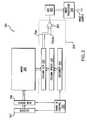
- FIG. 2illustrates a block diagram of a CMOS image sensor 201 , which can be operated in accordance with exemplary embodiments of the invention.
- Image sensor 201includes an imaging array 200 .
- Array 200comprises a plurality of pixels arranged in a predetermined number of columns and rows. The pixels of each row in array 200 are all turned on at the same time by a row selected line, and the pixels of each column are selectively output by respective column select lines. A plurality of rows and column lines are provided for the entire array 200 .
- the row linesare selectively activated in sequence by the row driver 258 in response to row address decoder 257
- the column select linesare selectively activated in sequence for each row activated by the column driver 255 in response to column address decoder 254 .
- a row and column addressis provided for each pixel cell.
- Image sensor 201is operated by the timing and control circuit 256 , which controls address decoders 257 , 254 for selecting the appropriate row and column lines for pixel readout, and row and column driver circuitry 258 , 255 which apply driving voltage to the drive transistors of the selected row and column lines. Exemplary timing for the operation of CMOS image sensor 201 according to embodiments of the invention is described in more detail below in connection with FIGS. 3-20 . According to embodiments of the invention a dual integration approach is used. Pixel cells of the array 200 each integrate light during a single integration period, and the length of an integration period for different pixel cells can be different, such that there are at least two integration periods for the array 200 as a whole.
- Pixel output signalstypically include a pixel reset signal V rst taken from the floating diffusion node when it is reset and a pixel image signal Vphoto which is taken from the floating diffusion region after photo-generated charge representing an image is transferred to the column sample and hold (S/H) circuit 253 .
- Voltages V rst and V photoare selected by the decoder 254 via the driver 255 and are subtracted by a differential amplifier 252 , which produces a differential signal, V rst -V photo , for each pixel cell, which represents the amount of light impinging on the pixel cells.
- This differential signalis digitized by an analog to digital converter (ADC) 251 .
- ADCanalog to digital converter
- the digitized pixel signalsare then fed to an image processor 250 to form a digital image.
- Analog signal processing circuit (ASP) 259comprises the column decoder 254 , the column driver 255 , the column sample and hold circuit 253 , and the amplifier 252 .
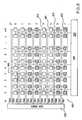
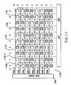
- FIG. 3depicts array 200 , which illustratively includes on-chip Red-Green-Blue primary color filters arranged in a Bayer pattern.
- a representative Bayer pattern unit 311is made up of a pixel cell 310 b associated with a red color filter, a pixel cell 310 c associated with a blue color filter, and two pixel cells 310 a , 310 d each associated with a green color filter.
- the color filterscan be other colors such as, e.g., a cyan-magenta-yellow Bayer pattern. Also, the color filters can be arranged in any appropriate pattern.
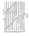
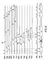
- FIG. 4is a timing diagram illustrating the operation of image sensor 201 including the imaging array 200 of FIG. 3 in accordance with an exemplary embodiment of the invention.
- the pixel cells of array 200have a 4T configuration as described in connection with FIG. 1 above.
- row driver 258In response to signals from timing and control circuitry 256 , row driver 258 outputs signals to each row such that pixels in Row 0, Row 1, Row 4, Row 5, have a first integration period and pixels in Row 2, Row 3, Row 6, Row 7 have a second integration period. Accordingly, there are two subsets of pixel cells in array 200 .
- the first subsetincludes pixel cells operated with an integration period 44 with a length of N, denoted by pixel cells 301 without cross hatching and the second subset includes pixel cells operated with an integration period 42 with a length of S, denoted by pixel cells 302 with cross hatching.
- the first and second subsetsare referred to as subsets 301 and 302 , respectively.
- the subsets 301 , 302include subgroups 315 of two adjacent rows. As shown in FIG. 3 , the first subset includes every other subgroup 315 beginning from an uppermost row, and the second subset includes the subgroups 315 not in the first subset.
- integration period 44is longer than integration period 42 .
- the integration period 44can be of a length equal to that of an integration period where image sensor 201 is operated in a conventional manner.
- the respective signals for each roware indicated in FIG. 4 , and other figures herein, by the signal notation followed by the corresponding row number, e.g., RST X and TX X, where X is the row number.
- FIG. 4depicts the operation of image sensor 201 , which includes array 200 .
- FIG. 4 and other timing diagrams contained hereinshow the operation of image sensor 201 where frames are consecutively readout. Accordingly, FIG. 4 , and other figures herein, depict portions of several frames. For simplicity, however, the operation of image sensor 201 is described with reference to a singly frame.
- pixel cells in Row 0are selected by applying a corresponding SEL 0 pulse (not shown) to activate a row select transistor 37 ( FIG. 1 ) in each of the pixel cells in Row 0.
- the pixel cells in each roware operated in a similar manner.
- the operation of pixel cells of array 200is described with reference to a single pixel cell of a row.
- V rstVaa_pix.
- chargeis accumulated during integration period 44 , which begins after the first illustrated TX 0 pulse.
- the accumulated chargeis transferred from photodiode 21 to floating diffusion region 3 by applying a pulse TX 0 to activate the gate of the transfer transistor 7 .
- the signal processing circuit 259uses the reset voltage signal, V rst , to obtain a differential signal.
- the differential signalcan be obtained during a horizontal blanking period (HBL), and the resulting output signal can be read out during the following horizontal scanning period when HD is high.
- “VBL” on FIG. 4denotes a vertical blanking period. To suppress blooming, it is desirable to keep a high RST voltage on the gate of the reset transistor 17 , as shown in FIG. 4 .
- Row 1is read out in a similar manner to that of Row 0 as shown in FIG. 4 .
- the pixel cells of Row 1also have an integration period 44 of length N. Therefore, pixel cells of subset 311 , which include a full Bayer pattern unit, have the same integration period 44 .
- Row 1After Row 1 is read out, the remaining rows of array 200 are read out sequentially beginning with Row 2.
- the remaining rows of array 200are read out in a similar manner to that of Row 0, except that alternating subgroups 301 , 302 of two adjacent rows have different integration period lengths N, S. Therefore, as shown in FIG. 4 , integration periods 42 for Rows 2, 3, 6, and 7 have a length S, which is illustratively shorter than the length N; and integration periods 44 for Rows 4 and 5 have a length N. In this manner, a dual integration approach with two different lengths of signal integration periods can be realized.
- a respective RST 3 signalis pulsed high after readout of V photo from a previous frame.
- RST 3remains high at the beginning of the integration period 42 .
- TX 3is pulsed high to activate the gate of the transfer transistor 7 and reset the photodiode 21 to a predetermined voltage to begin the integration period 42 .
- FIG. 5illustrates a pulse timing diagram for an exemplary operation of image sensor 201 where pixel cells of array 200 are operated in a global rest mode.
- a global reset techniqueis only shown in FIG. 5 with respect to array 200 , but it should be appreciated that a global reset technique can be implemented in all embodiments of the invention described herein.
- all pixel cells of array 200are reset simultaneously by pulsing corresponding RST X signals high to operate the gates of respective reset transistors 17 to reset respective floating diffusion regions to a predetermined voltage, which is illustratively Vaa_pix. Also, corresponding TX X signals are pulsed high to reset respective photodiodes 21 to a predetermined voltage, in this exemplary embodiment, Vaa_pix.
- a corresponding TX 0 signalis cycled low to begin the integration period having length N while a corresponding RST 0 signal remain high.
- a corresponding RST 0 signalis cycled low.
- a corresponding TX 0 signalis pulsed high to activate the gate of transfer transistor to transfer charge accumulated by photodiode 21 to floating diffusion region 3 .
- a corresponding RST 2 and TX 2 signalremain high at the beginning of the integration period 42 .
- TX 2 signalsis cycled low to begin the integration period 42 .
- a corresponding TX 2 signalis pulsed high to activate respective gate of transfer transistor 7 to transfer charge accumulated by photodiode 21 to floating diffusion region 3 .
- integration periods 42 , 44 for all pixel cells of array 200end at a same time when charge accumulated by respective photodiodes 21 is transferred to respective floating diffusion regions 3 . Subsequently, the charge on floating diffusion regions 3 is readout row by row as shown in FIG. 5 .
- image sensor 201can include an array of pixel cells 600 , as shown in FIG. 6 , instead of array 200 ( FIG. 3 ).
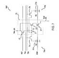
- Array 600is similar to array 200 except that pixel cells of array 600 have a shared column configuration. Accordingly, pixel cells in a pixel unit 660 share readout circuitry 75 , as shown in FIG. 7 .
- there are two subsets of pixel cells in array 600The first subset includes pixel cells operated with an integration period 44 ( FIG. 8 ) having length N, denoted by pixel cells 601 without cross hatching, and the second subset includes pixel cells operated with an integration period 42 ( FIG. 8 ) having length S, denoted by pixel cells 602 with cross hatching.
- the first and second subsetsare referred to as subsets 601 and 602 , respectively.
- the subsets 601 , 602include subgroups 615 of two adjacent rows. As shown in FIG. 6 , the subset 601 includes every other subgroup 615 beginning from an uppermost row, and the subset 602 includes the subgroups 615 not in the subset 601 .
- FIG. 7depicts pixel cells 70 a and 70 b having a shared column configuration in array 600 .
- Pixel cells 70 a , 70 beach include a photo-conversion device, for example a photodiode 21 a and 21 b , respectively.
- pixel cells 70 a and 70 beach respectively include a transfer transistor 7 a and 7 b controlled by a TXa and TXb signal, respectively.
- Both pixel cells 70 a and 70 bshare readout circuitry 75 , which illustratively includes a floating diffusion region 3 , source follower transistor 27 and row select transistor 37 .
- the components of pixel cells 70 a and 70 bperform the same functions as the corresponding components described above in connection with FIG. 1 .
- the operation of array 600is changed to accommodate the shared column configuration.
- FIG. 8depicts exemplary timing for the operation of image sensor 201 including array 600 .
- pixel cells in Row 0are selected by applying a corresponding SEL 0 pulse (not shown) to activate a row select transistor 37 ( FIG. 1 ) in each of the pixel cells in Row 0.
- pixel units 660 of each roware operated in a similar manner. For simplicity, the operation of pixel units 660 of array 600 is described with reference to a single pixel unit 660 of a row.
- V rstVaa_pix.
- pixel cells of Row 0accumulate charge during integration period 44 , which has a length N.
- the integration period 44begins after charge from a previous frame is read out and as TXa 0 or TXb 0 goes low.
- charge accumulated during an integration period 44 having a length Nis transferred from photodiode 21 a to floating diffusion region 3 by applying a pulse TXa 0 to activate the gate of the transfer transistor 7 a .
- the signal voltage, V photo-arepresenting the charge accumulated by photodiode 21 a during integration period 44 is read out to the signal processing circuit 259 as SHS is pulsed high to sample and hold V photo-a .
- this procedurecan be performed during the first half of a horizontal blanking period HBL.
- RST 0is pulsed high to activate the gate of the reset transistor 17 to reset the floating diffusion region 3 to Vaa_pix and a reset signal, V rst , is applied to the gate of the source follower transistor 27 and readout via column line 40 to the analog signal processing circuit 259 as SHR is pulsed high to sample and hold V rst .
- the charge accumulated by photodiode 21 b during its integration period 44is readout and transferred to floating diffusion region 3 by applying a pulse TXb 0 to activate the gate of the transfer transistor 7 b .
- the signal voltage, V photo-brepresenting the charge accumulated by photodiode 21 b during integration period 44 is read out to the signal processing circuit 259 as SHS is pulsed high to sample and hold V photo-b .
- the signal processing circuit 259uses the reset voltage signal, V rst , to obtain a differential signal. As shown in FIG. 8 , this procedure can be performed during the latter half of a horizontal blanking period HBL, and the resulting output signal in a row can be read out during a following horizontal scanning period when HD is high.
- Row 1is read out in a similar manner to that of Row 0 as shown in FIG. 8 .
- Pixel cells of Row 1also have an integration period 44 with a length N.
- the remaining rows of array 600are read out sequentially beginning with Row 2.
- the remaining rows of array 600are is also read out in a similar manner to that of Row 0, except that alternating subsets of two adjacent rows have different integration period lengths N, S. Therefore, as shown in FIG. 8 , integration periods 42 for Rows 2, 3, 6, and 7 have a length S, which is illustratively shorter than the length N; and integration periods 44 for Rows 4 and 5 have a length N. In this manner, a dual integration period approach with two different lengths of signal integration periods can be realized.
- TXa 2 signalis pulsed high to activate the gate of the transfer transistor 7 a , 7 b and reset the photodiode 21 a , 21 b to a predetermined voltage, which is Vaa_pix in the exemplary embodiment of FIG. 6 , to begin the integration period 42 .
- TXa, TXb, SHSare used to read out V photo-a , V photo-b for Row 2.
- FIG. 9is a graph depicting the light transfer characteristics of image sensor 201 operated as described above in connection with FIGS. 4-8 .
- Pixel cells having a shorter integration period 42represented by line 902
- have an output corresponding to a wider range of luminance than do the pixel cells having a longer integration period 44represented by line 901 .
- the outputs from pixel cells having both lengths of integration periods 44 , 42are used to achieve a synthetic output and a wide dynamic range.
- R(i,j)An original signal output at column i and row j is expressed as S(i,j).
- the synthesized signal output R(i,j)is the sum of the same color signal of S(i,j) and S(i,j+2).
- a green color signal S(0,0)is added to a green color signal S(0,2). This procedure achieves a wide dynamic range, but degrades a vertical resolution by a half of its original resolution. If sensor array 200 , 600 has a sufficient number of pixel cells, however, such as a 4 Mega pixel array, a high quality image can still be achieved.
- an interpolation procedurecan be used.
- An original signal output at column i and row jis expressed as S(i,j).
- n, n +1(equation 3)
- n and n′are row numbers following the respective sequences provided for equations 3 and 4.
- parameters A-Dprovide the relative proportions of the signals that make up a synthetic signal R(i,j).
- the parameters A through Dcan be changed continuously depending upon the light intensity.
- the integration periods 44 , 42can be changed adaptively depending upon the light intensity of the imaged scene. For example, at low light levels, S can be set to equal N and as light levels increase, S can be reduced as compared to N.
- image processor 250After interpolation is performed, two sets of image data, original signals S(i,j) and synthetic signals R(i,j), are processed by image processor 250 to reproduce a wide dynamic range image having a resulting light transfer characteristic as depicted by line 903 in FIG. 9 .
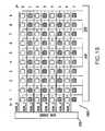
- FIG. 11depicts an array 1100 , which can be implemented in image sensor 201 ( FIG. 2 ) and operated according to another exemplary embodiment of the invention.
- Pixel cells in the embodiment of FIG. 11are divided into two subsets: subset 1101 depicted as pixel cells without cross hatching and 1102 depicted as pixel cells with cross hatching.
- subset 1101depicted as pixel cells without cross hatching
- 1102depicted as pixel cells with cross hatching.
- subset 1101has an integration period 44 with a length N
- subset 1102has an integration period 42 with a length S.
- Pixel cells of subset 1101 and 1102are arranged such that the subsets include subgroups 1115 of four pixel cells spanning two adjacent rows and two adjacent columns.
- the subset 1101includes every other subgroup 1115 and subset 1102 includes subgroups 1115 that are not in subset 1101 , such that the subsets form a checker board-like (zigzag) pattern as shown in FIG. 11 .
- array 1100includes color filters associated with each pixel cell and arranged in a Bayer pattern. Therefore, each subgroup includes four color filters which make up a Bayer pattern unit. This arrangement enables good balancing of resolution in both the horizontal and vertical directions.
- Row select lines 1136 - 1 and 1136 - 2respectively associated with each row of array 1100 .
- Row select lines 1136 - 1 and 1136 - 2respectively carry signals to pixel cells of subsets 1101 and 1102 to activate row select transistor 37 ( FIG. 1 ) in respective pixel cells for readout of those pixel cells.
- An image sensor 201which includes array 1100 of FIG. 11 , can be operated as described above in connection with FIGS.
- pixel cells of each roware read out in two readout processes, one readout process includes reading out pixel cells of subset 1101 , which have an integration period 44 , the second readout process includes reading out pixel cells of subset 1102 , which have an integration period 42 .
- the outputs from pixel cells having integration periods 44 , 42are used to achieve a synthetic output and a wide dynamic range, as described above.
- FIG. 12is an exemplary timing diagram depicting the operation of pixel cells of Row 0 (of array 1100 ).
- the respective signals for each roware indicated in FIG. 11 , and other subsequent figures herein, by the signal notation followed by the corresponding row number, e.g., RST X-W and TX X, where X is the row number and W is the subset number.
- pixel cells of subset 1101are selected by applying a corresponding SEL 0-1101 pulse (not shown) to activate a row select transistor 37 ( FIG. 1 ) in each of the pixel cells in subset 1101 of Row 0.
- each rowis operated in a similar manner.
- the operation of array 1100is described with reference to a single row.
- V rstVaa_pix.
- Pixel cells of subset 1101 in Row 0accumulate charge during integration period 44 , which has a length N.
- the integration period 44begins as TX 0-1101 goes low, ending the readout of a previous frame.
- chargeis transferred from photodiode 21 to floating diffusion region 3 by applying a pulse TX 0-1101 to activate the gate of the transfer transistor 7 .
- the signal voltage, V photo1101representing the charge accumulated during integration period 44 is applied to the gate of the source follower transistor 27 and read out via column line 40 .
- SHSgoes is pulsed high to sample and hold V photo1101 .
- this procedurecan be performed during the first half of a horizontal blanking period HBL.
- Pixel cells of subset 1102are read out. Pixel cells in Row 0 of subset 1102 are selected by applying a corresponding SEL 0-1102 pulse (not shown) to activate a row select transistor 37 in each of the pixel cells in Row 0 of subset 1102 . Pixel cells of subset 1102 are read out in a similar manner to that of pixel cells of subset 1101 .
- pixel cells of subset 1102are operated to have a shorter integration period than pixel cells of subset 1101 .
- a RST 0-1102 signalis pulsed high.
- RST 0-1102remains high at the beginning of the integration period 42 of length S.
- RST 0-1102is cycled to low and TX 0-1102 is pulsed high to activate the gate of the transfer transistor 7 and reset the photodiode 21 to a predetermined voltage, which is Vaa_pix in the exemplary embodiment of FIG. 12 .
- TX 0-1102goes low the integration period 42 begins.
- TX 0-1102is pulsed high and the charge can be read out at SHS.
- This procedurecan be perfumed during the latter half of a horizontal blanking period HBL, and the resulting output signal in a row can be read out during a following horizontal scanning period when HD is high, as shown in FIG. 12 .
- FIGS. 11-12can be adapted for an array having pixel cells with a shared column configuration.
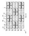
- FIG. 13shows an array 1300 including pixel cells having a shared column configuration.
- Array 1300can be implemented in image sensor 201 .
- Array 1300can be operated to realize a wide dynamic range with high density and well balanced spatial resolution.
- array 1300includes two subsets, subset 1301 , depicted as including pixel cells without a shaded background, and subset 1302 , depicted as including pixel cells with a shaded background.
- the subsets 1301 , 1302include subgroups 1315 of four pixel cells spanning two adjacent rows and two adjacent columns.
- the subsets 1301 , 1302form a checker board-like (zigzag) pattern as shown in FIG. 13 .
- Array 1300is configured such that pixel cells of the subset 1301 have an integration period 44 with a length N, and pixels cells of subset 1302 have an integration period 42 with a length S as shown in FIG. 14 .
- array 1300includes color filters associated with each pixel cell and arranged in a Bayer pattern. Therefore, each subgroup 1315 includes four color filters which make up a Bayer pattern unit.
- Pixel cells of array 1300are configured as shown in FIG. 7 , such that two adjacent pixel cells within a row share readout circuitry 75 , and make up a shared column pixel unit 1360 .
- one pixel cell 1316 of a shared column pixel unit 1360is part of subset 1301 and the other pixel cell 1317 is part of subset 1302 .
- pixel cells of subset 1301can be configured to include only pixel cells 70 a
- subset 1302can be configured to include only pixel cells 70 b
- pixel cells 70 acan be operated to have an integration period 44
- pixel cells 70 bcan be operated to have an integration period 42 .
- FIG. 14is a timing diagram depicting an exemplary operation of array 1300 .
- pixel cells in Row 0are selected by applying a corresponding SEL 0 pulse (not shown) to activate a row select transistor 37 ( FIG. 1 ) in each of the pixel cells in Row 0.
- shared column pixel units 1360 of each roware operated in a similar manner. For simplicity, the operation of units 1360 of array 1300 is described with reference to a single shared column pixel unit 1360 of a row.
- V rstVaa_pix.
- Pixel cells of subset 1301 in Row 1accumulate charge during an integration period 44 , which has a length N.
- the integration period 44begins as TXa 0 goes low, ending the readout of a previous frame.
- Charge accumulated during integration period 44is transferred from photodiode 21 a to floating diffusion region 3 by applying a pulse TXa 0 to activate the gate of the transfer transistor 7 a .
- the signal voltage, V photo-arepresenting the charge accumulated by photodiode 21 a during integration period 44 is read out to the signal processing circuit 259 as SHS is pulsed high to sample and hold V photo-a .
- this procedurecan be performed during the first half of a horizontal blanking period HBL.
- RST 0is pulsed high to activate the gate of the reset transistor 17 to reset the floating diffusion region 3 to Vaa_pix and a reset signal, V rst , is applied to the gate of the source follower transistor 27 and readout via column line 40 to the analog signal processing circuit 259 as SHR is pulsed high to sample and hold V rst .
- a respective TXb signalis pulsed high to activate the gate of the transfer transistor 7 b and reset the photodiode 21 b to a predetermined voltage, which is illustratively Vaa_pix, to begin the integration period 42 .
- Charge accumulated by photodiode 21 b during an integration period 42 with length Sis readout similarly to the readout of V photo-a , described above.
- the charge accumulated by photodiode 21 bis transferred from photodiode 21 b to floating diffusion region 3 by applying a pulse TXb 0 to activate the gate of the transfer transistor 7 b .
- the signal voltage, V photo-brepresenting the charge accumulated by photodiode 21 b during integration period 42 is read out to the signal processing circuit 259 as SHS is pulsed high to sample and hold V photo-b .
- SHSsample and hold V photo-b
- this procedurecan be performed during the latter half of a horizontal blanking period HBL.
- the resulting output signal in a rowcan be read out during a following horizontal scanning period when HD is high.
- the signal processing circuit 259uses the reset voltage signal, V rst , to obtain a differential signal as described above.
- Row 1 and the remaining rows of array 1300are read out in a similar manner to that of Row 0, as shown in FIG. 14 .
- a dual integration period approach with two different lengths of signal integration periodscan be realized.
- the outputs from pixel cells having both lengths N, S of integration periods 44 , 42are used to achieve a synthetic output and a wide dynamic range.
- a simple procedure to achieve a synthetic outputis to add two pixel signals.
- An original signal output at column i and row jis expressed as S(i,j).
- n, n+ 1(equation 5)
- n and n′are row numbers following the respective sequences provided for equations 5 and 6. This procedure achieves a wide dynamic range, but it degrades an original spatial resolution.
- parameters A to Dprovide the relative proportions of the signals that make up a synthetic signal R(i,j).
- the parameters A to Dcan be changed continuously depending upon the light intensity.
- the integration periods 44 , 42can be changed adaptively depending upon the light intensity. For example, at low light levels, S can be set to equal N and as light levels increase, S can be reduced as compared to N.
- FIG. 15depicts an array 1500 , which can be implemented in image sensor 201 ( FIG. 2 ) and operated according to another exemplary embodiment of the invention.
- Pixel cells in the embodiment of FIG. 15can have a single ( FIG. 1 ) or shared column configuration ( FIG. 7 ) and are divided into two subsets: subset 1501 , which is depicted as including pixel cells without cross hatching, and subset 1502 , which is depicted as including pixel cells with cross hatching.
- subset 1501has an integration period with length N
- subset 1502has an integration period with length S.
- Pixel cells of subset 1501are arranged such that subset 1501 includes three pixel cells of a Bayer pattern unit, each associated with a different colored filter.
- a Bayer pattern unitcan include a two pixel cells respectively associated with red and green filters in a row directly above two pixel cells respectively associated with blue and green color filters. Therefore, as shown in FIG. 15 , subset 1501 includes three pixel cells respectively associated with red, green, and blue color filters.
- Pixel cells of subset 1502include a pixel cell associated with the redundant color filter in a Bayer pattern unit, illustratively green.
- array 1500can have two row select lines 1536 - 1 and 1536 - 2 respectively associated with each of the rows of array 1500 .
- rows including only pixel cells of subset 1501can have a single row select line, while rows including pixel cells of subsets 1501 and 1502 can have two row select lines.
- Pixel cells of array 1500can be read out in a similar manner to pixel cells of arrays 200 , 600 , 1100 , and/or 1300 , described above with respect to FIGS. 2-14 .
- the operation of array 1500can be adapted to achieve a different integration period 44 , 42 for each subset 1501 , 1502 as described above with respect to FIGS. 2-14 . Accordingly, for simplicity, specific examples of timing for the operation of array 1500 are not shown.
- the signal of pixel cells of subset 1502can be treated as a luminance signal without chrominance signals.
- the pixel cells of subset 1502can be used as the luminance response for pixel cells of subset 1501 . Thereby, especially under conditions of strong illumination such that the pixel cells of subset 1501 are saturated, a wide dynamic range is achieved.
- Pixel cells of subset 1501which have an integration period of length N, become saturated and alone yield a narrower dynamic range as depicted by reference numeral 1601 .
- Pixel cells of subset 1502have an integration period of length S and do not become readily saturated, thereby allowing a wider dynamic range depicted by reference numeral 1602 .
- FIG. 17depicts an exemplary method for acquiring color information under conditions of strong illumination.
- a sceneis imaged toward the light source illuminating the scene, some part of an image frame is occupied by a strongly illuminated area.
- a sceneis an outdoor scene including a bright sky, as shown in FIG. 17 .
- the perimeter 1705 of the imaging arraycan be used to acquire color information by operating pixel cells in the perimeter with an integration period 42 with a length S.
- the pixel cells in the perimeter 1705include those associated with full pattern units of the color filter array pattern, e.g., a Bayer pattern.
- FIG. 17depicts an exemplary method for acquiring color information under conditions of strong illumination.
- the perimeter 1705includes two uppermost rows, two lowermost rows, two leftmost columns, and two rightmost columns. Different numbers of rows and columns can also constitute perimeter 1705 .
- array 1500can be easily adapted to achieve this operation based on the teachings of this specification.
- the color information from perimeter 1705 pixel cellscan be used to achieve a synthetic signal representing the strongly illuminated area.
- Color information from the perimeter 1705 pixel cellscan be used to “paint” the signals for those pixel cells of the central portion 1704 , which correspond to the strongly illuminated area.
- color information obtained from perimeter pixel cellscan be used to achieve color information for those pixel cells receiving light from the strongly illuminated area.
- FIG. 18shows how to acquire a color signal for such a scene.
- the graphs of FIG. 18represent the response of pixel cells of array 1500 along line 18 - 18 ′, which include pixel cells that receive light from a strongly illuminated area.
- signals of pixel cells of subset 1501are saturated, but pixel cells receiving light from the fringes of the strongly illuminated object are not saturated.
- a chrominance signalcan be obtained from pixel cells of subset 1501 receiving light from the fringe area. This chrominance signal can be used to achieve color information for those pixel cells receiving light from the strongly illuminated area.
- FIGS. 2-18provide dual integration period operations for image sensors including arrays that have color filters.
- the inventionis not so limited.
- the techniques discussed abovecan also be adapted for monochromatic imaging devices.
- a monochromatic imaging array 1900 to achieve wide dynamic rangeis shown in FIG. 19 .
- Pixel cells in rows 0, 2, 4 . . .are set to have an integration period with length N (not shown), and pixel cells in rows 1, 3, 5 . . . are set to have an integration period with length S (not shown).
- An image sensor 201 including array 1900can be operated according to the timing shown in FIG. 4 , except that alternating rows will be configured to have different integration periods.
- pixel cells of array 2000can have a configuration as depicted in FIG. 1 or a shared column configuration depicted in FIG. 7 .
- R(i,j)An original signal output at column i and row j is expressed as S(i,j).
- n and n′are row numbers following the respective sequences provided for equations 11 and 12.
- the parameters A through Dcan be changed continuously depending upon the light intensity.
- the integration periods 44 , 42can be changed adaptively depending upon the light intensity of the imaged scene. For example, at low light levels, S can be set to equal N and as light levels increase, S can be reduced as compared to N.
- FIG. 20shows another embodiment for monochromatic array 2000 , which is similar to the arrays of FIGS. 11-14 .
- Pixel cells of array 2000are arranged in subsets 2001 , depicted as including pixel cells without cross hatching, and 2002 , depicted as including pixel cells with cross hatching.
- Subset 2001includes every other pixel cell in a row and every other pixel cell in a column
- the subset 2002includes the pixel cells that are not in the first subset, such that the first and second subsets form a checker board-like (zigzag) pattern, as shown in FIG. 20 .
- Pixel cells of array 2000can have a configuration as depicted in FIG. 1 or a shared column configuration depicted in FIG. 7 .
- Pixel cells of subset 2001are operated to have an integration period with length N
- pixel cells of subset 2002are operated to have an integration period with length S.
- the exemplary embodiment of FIG. 20provides well balanced horizontal and vertical resolutions in wide dynamic range operation.
- Image sensor 201 including array 2000can be operated as shown in FIGS. 12 and 14 .
- n and n′are row numbers following the respective sequences provided for equations 13 and 14. This procedure achieves a wide dynamic range, but it degrades an original spatial resolution.
- the parameters A through Dcan be changed continuously depending upon the light intensity.
- the integration periods 44 , 42can be changed adaptively depending upon the light intensity of the imaged scene. For example, at low light levels, S can be set to equal N and as light levels increase, S can be reduced as compared to N.
- CMOS pixel cellshaving particular configurations
- the inventioncan be implemented using CMOS pixel cells having alternative configurations.
- CMOS pixel cells having additional circuitrye.g., anti-blooming circuitry or electronic shutter circuitry
- additional circuitrye.g., anti-blooming circuitry or electronic shutter circuitry
- embodiments of the inventionare described in connection with particular timing operations, the invention is not so limited. Additional timing operations can be used and modifications to the timing shown can be made, which are within the scope of the invention. For example, where pixel cells include an electronic shutter, operation of the image sensor can be accordingly adapted.
- FIG. 21is a block diagram of an image sensor 2101 , which includes automatic exposure control circuitry 2103 .
- automatic exposure controlis performed by varying an aperture condition 2102 , e.g., an integration period and an iris of lens, by checking the signal output at every frame.
- An exemplary method for conventional automatic exposure controlis discussed in U.S. Pat. No. 6,486,915, which is incorporated herein by reference.
- embodiments of the inventionprovide two sets of signals each having a different integration period 44 , 42 .
- the automatic control circuitry 2103can use the two sets of signals to determine a proper aperture condition 2102 , thereby reducing the time for automatic exposure control and providing more efficient operation as compared to the case where only a single integration period is used.
- conventional automatic exposure control techniques and circuitrycan be readily adapted to accommodate the two sets of signals provided by embodiments of the present invention.
- a processor based system 2200which includes a CMOS image sensor according to the invention is illustrated generally at 2221 in FIG. 22 .
- Processor based system 2200is exemplary of a system having digital circuits, which could include an image sensor. Without being limiting, such a system could include a computer system, camera system, scanner, machine vision, vehicle navigation, video phone, surveillance system, auto focus system, star tracker system, motion detection system, image stabilization system and data compression system for high-definition television, all of which can utilize the present invention.
- Processor based system 2200such as a computer system, for example generally comprises a central processing unit (CPU) 2226 , for example, a microprocessor, which communicates with an input/output (I/O) device 2222 over a bus 2225 .
- the CMOS image sensor 2221also communicates with the system over bus 2225 .
- the computer system 2200also includes random access memory (RAM) 2223 , and, in the case of a computer system may include peripheral devices such as a floppy drive 2227 , or a compact disk (CD) ROM drive 2228 which also communicate with CPU 2226 over the bus 2225 . It may also be desirable to integrate the processor 654 , CMOS image sensor 2221 and memory 2223 on a single IC chip.
Landscapes
- Engineering & Computer Science (AREA)
- Multimedia (AREA)
- Signal Processing (AREA)
- Physics & Mathematics (AREA)
- Spectroscopy & Molecular Physics (AREA)
- Solid State Image Pick-Up Elements (AREA)
- Color Television Image Signal Generators (AREA)
- Transforming Light Signals Into Electric Signals (AREA)
Abstract
Description
- The present invention relates to the field of semiconductor devices, particularly to the operation of an image sensor to achieve improved dynamic range.
- Complimentary Metal Oxide Semiconductor (CMOS) Active Pixel Sensors (APS) are increasingly being used as a lower cost alternative to Charge Coupled Devices (CCDs). A CMOS image sensor circuit includes a focal plane array of pixel cells, each one of the cells includes a photo-conversion device, such as a photogate, photoconductor, or photodiode, for accumulating photo-generated charge. Each pixel cell may include a transistor for transferring charge from the photo-conversion device to a sensing node, and a transistor, for resetting a sensing node to a predetermined charge level prior to charge transfer. The pixel cell may also include a source follower transistor for receiving and amplifying charge from the sensing node and an access transistor for controlling the readout of the cell contents from the source follower transistor.
- In a CMOS image sensor, the active elements of a pixel cell perform the necessary functions of: (1) photon to charge conversion; (2) accumulation of image charge; (3) transfer of charge to the sensing node accompanied by charge amplification; (4) resetting the sensing node to a known state before the transfer of charge to it; (5) selection of a pixel for readout; and (6) output and amplification of a signal representing pixel charge from the sensing node.
- CMOS image sensors of the type discussed above are generally known as discussed, for example, in Nixon et al., “256×256 CMOS Active Pixel Sensor Camera-on-a-Chip,” IEEE Journal of Solid-State Circuits, Vol. 31(12), pp. 2046-2050 (1996); and Mendis et al., “CMOS Active Pixel Image Sensors,” IEEE Transactions on Electron Devices, Vol. 41(3), pp. 452-453 (1994).
- A conventional
CMOS pixel cell 10 is illustrated inFIG. 1 . TheCMOS pixel cell 10 is a four transistor (4T) cell.Pixel cell 10 comprises a photo-conversion device, typically aphotodiode 21, for collecting charges generated by light incident on the pixel cell. Atransfer transistor 7, when activated by a transfer control signal TX, transfers photoelectric charges from thephotodiode 21 to a sense node (charge to voltage conversion node), typically afloating diffusion region 3. Areset transistor 17 resets thefloating diffusion region 3 to a predetermined voltage, Vaa_pix, in response to a reset control signal RST before thefloating diffusion region 3 receives photo-generated charge.Floating diffusion region 3 is also electrically connected to the gate of an outputsource follower transistor 27.Pixel cell 10 also includes a rowselect transistor 37 for outputting a signal representing the charge on thefloating diffusion region 3 from thesource follower transistor 27 to anoutput column line 40 in response to an address signal SEL. - In the
pixel cell 10 depicted inFIG. 1 , the photo-conversion device generates and accumulates charge, e.g., electrons, in response to incident light during an integration period. The charge is transferred to thefloating diffusion region 3 by activating the gate of thetransfer transistor 7. Thesource follower transistor 27 produces an output signal from the transferred charges, which is readout via thecolumn line 40. - A typical CMOS image sensor includes an array of
pixels 10, arranged in a predetermined number of columns and rows. Generally, each pixel generates charge for a same amount of time. Such image sensors have a characteristic dynamic range. Dynamic range refers to the range of incident light that can be accommodated by an image sensor in a single frame of pixel data. It is desirable to have an image sensor with a high dynamic range to image scenes that generate high dynamic range incident signals, such as indoor rooms with windows to the outside, outdoor scenes with mixed shadows and bright sunshine, night-time scenes combining artificial lighting and shadows, and many others. - The dynamic range for an image sensor is commonly defined as the ratio of its largest non-saturating signal to the standard deviation of the noise under dark conditions. Dynamic range is limited on an upper end by the charge saturation level of the sensor, and on a lower end by noise imposed limitations and/or quantization limits of the analog to digital converter used to produce the digital image. When the dynamic range of an image sensor is too small to accommodate the variations in light intensities of the imaged scene, image distortion occurs.
- As pixel size is scaled down, so is the size of the photo-conversion device. Therefore, the amount of charge the photo-conversion device and pixel cell can accumulate is reduced, degrading the sensor's dynamic range. There are several approaches to improve dynamic range, one of which utilizes dual integration periods. Another approach would be to add transistors to the pixel. Since it is difficult to implement additional transistors inside a pixel while at the same time maintaining a small pixel size (e.g., less than approximately 3.2 μm), the dual integration period approach is more desirable because the pixel cell can remain the same and only pulse timing related modifications are needed.
- Orly Yadid-Pecht et al. in the article “Wide Intrascene Dynamic Range CMOS APS Using Dual Sampling,” IEEE Transactions of Electron Devices, Vol. 44, No. 10, pp. 1721-1723 (October 1997) (“Yadid-Pecht”) discloses a method of operating an image sensor where, for each frame, the output data includes two sets of pixel cell outputs each having different integration periods. The image sensor according to Yadid-Pecht requires additional column signal processing circuitry above the pixel cell array. Additionally, the methods disclosed by Yadid-Pecht are not well suited to color imaging.
- Wandell et al., “Multiple Capture Single Image Architecture with a CMOS Sensor,” Chiba Conference on Multispectral Imaging, pp. 11-17 (1999) (“Wandell”) disclosed an imaging method using multiple integration periods. With the method described by Wandell, a CMOS image sensor includes one analog to digital converter (ADC) for each 2×2 pixel cell block. The pixel cells of each block are switchably connected to a storage capacitor, which in turn is connected to the ADC. Thus, the method of Wandell requires additional circuitry and cannot be implemented using conventional CMOS image sensor circuits, which is undesirable.
- U.S. Pat. No. 6,008,486 to Stam et al. (“Stam”) discloses a method using dual integration periods. With Stam's method, each pixel cell integrates charge during a short integration period and a long integration period for each frame. If the pixel cell becomes saturated during the long integration period, a threshold detector causes the short integration period for that pixel cell to be used. Because each pixel cell integrates charge for two time periods per frame, additional sample and hold circuitry is required, which is undesirable.
- What is needed, therefore, is a method for operating a CMOS image sensor to achieve an improved dynamic range, which can be implemented using conventional CMOS pixel cells. Additionally, it would be advantageous to have an improved method for operating a CMOS image sensor to achieve an improved dynamic range that is also well suited to color imaging.
- Embodiments of the invention provide a method and apparatus that allow for wide dynamic range operations of CMOS Active Pixel Sensors. In an array of pixel cells, first charge is accumulated in a first subset of pixel cells during a first integration period and second charge is accumulated in a second subset of pixel cells during a second integration period. A length of the first integration period is different than a length of the second integration period, and the first and second charge are accumulated during a same frame are read out.
- The foregoing and other aspects of the invention will be better understood from the following detailed description of the invention, which is provided in connection with the accompanying drawings, in which:
FIG. 1 is a schematic diagram of a conventional pixel cell;FIG. 2 is a block diagram illustrating an image sensor according to an exemplary embodiment of the invention;FIG. 3 is a block diagram illustrating a portion of the image sensor ofFIG. 2 according to an exemplary embodiment of the invention;FIG. 4 is a timing diagram illustrating the operation of the image sensor ofFIGS. 2 and 3 according to an exemplary embodiment of the invention;FIG. 5 is a timing diagram illustrating the operation of the image sensor ofFIGS. 2 and 3 according to another exemplary embodiment of the invention;FIG. 6 is a block diagram illustrating a portion of the image sensor ofFIG. 2 according to another exemplary embodiment of the invention;FIG. 7 is a schematic diagram of pixel cells having a shared column configuration, which can be implemented in the array ofFIG. 6 ;FIG. 8 is a timing diagram illustrating the operation of the image sensor ofFIGS. 2 and 6 according to another exemplary embodiment of the invention;FIG. 9 is a graph illustrating the light transfer characteristics of the image sensor operated as described above in connection withFIGS. 4-8 ;FIG. 10 is a block diagram illustrating interpolation for pixel cells of the image sensors ofFIGS. 2, 3 , and6 according to another exemplary embodiment of the invention;FIG. 11 is a block diagram illustrating a portion of the image sensor ofFIG. 2 according to another exemplary embodiment of the invention;FIG. 12 is a timing diagram illustrating the operation of the image sensor ofFIGS. 2 and 11 according to another exemplary embodiment of the invention;FIG. 13 is a block diagram illustrating a portion of the image sensor ofFIG. 2 according to another exemplary embodiment of the invention;FIG. 14 is a timing diagram illustrating the operation of the image sensor ofFIGS. 2 and 13 according to another exemplary embodiment of the invention;FIG. 15 is a block diagram illustrating a portion of the image sensor ofFIG. 2 according to another exemplary embodiment of the invention;FIG. 16 is a graph illustrating the light transfer characteristics of the image sensor ofFIG. 15 under conditions of strong illumination;FIG. 17 is a diagram illustrating the array ofFIG. 15 according to another exemplary embodiment of the invention;FIG. 18 is a diagram illustrating the operation of the image sensor ofFIG. 15 according to another exemplary embodiment of the invention;FIG. 19 is a block diagram illustrating a portion of the image sensor ofFIG. 2 according to another exemplary embodiment of the invention;FIG. 20 is a block diagram illustrating a portion of the image sensor ofFIG. 2 according to another exemplary embodiment of the invention;FIG. 21 is a block diagram illustrating of an image sensor according to another exemplary embodiment of the invention; andFIG. 22 is a block diagram illustrating a processor system according to an exemplary embodiment of the invention.- In the following detailed description, reference is made to the accompanying drawings, which form a part hereof and illustrate specific embodiments in which the invention may be practiced. In the drawings, like reference numerals describe substantially similar components throughout the several views. These embodiments are described in sufficient detail to enable those skilled in the art to practice the invention, and it is to be understood that other embodiments may be utilized, and that structural, logical and electrical changes may be made without departing from the spirit and scope of the present invention.
- The term “pixel” or “pixel cell” refers to a picture element unit cell containing a photo-conversion device and associated transistors or other circuitry that convert electromagnetic radiation to an electrical signal. For purposes of illustration, representative pixel cells are illustrated in the figures and description herein, and typically all pixels in an image sensor will have a similar configuration.
- The invention provides embodiments in which a dual integration period approach is used to capture a wide dynamic range image. As described in more detail below, these methods are particularly useful in an on-chip color filtered CMOS APS. The invention, however, is not so limited and, as described below, is applicable to other image sensors.
FIG. 2 illustrates a block diagram of aCMOS image sensor 201, which can be operated in accordance with exemplary embodiments of the invention.Image sensor 201 includes animaging array 200.Array 200 comprises a plurality of pixels arranged in a predetermined number of columns and rows. The pixels of each row inarray 200 are all turned on at the same time by a row selected line, and the pixels of each column are selectively output by respective column select lines. A plurality of rows and column lines are provided for theentire array 200. The row lines are selectively activated in sequence by therow driver 258 in response torow address decoder 257, and the column select lines are selectively activated in sequence for each row activated by thecolumn driver 255 in response tocolumn address decoder 254. Thus, a row and column address is provided for each pixel cell.Image sensor 201 is operated by the timing andcontrol circuit 256, which controlsaddress decoders column driver circuitry CMOS image sensor 201 according to embodiments of the invention is described in more detail below in connection withFIGS. 3-20 . According to embodiments of the invention a dual integration approach is used. Pixel cells of thearray 200 each integrate light during a single integration period, and the length of an integration period for different pixel cells can be different, such that there are at least two integration periods for thearray 200 as a whole.- Pixel output signals typically include a pixel reset signal Vrsttaken from the floating diffusion node when it is reset and a pixel image signal Vphoto which is taken from the floating diffusion region after photo-generated charge representing an image is transferred to the column sample and hold (S/H)
circuit 253. Voltages Vrstand Vphotoare selected by thedecoder 254 via thedriver 255 and are subtracted by adifferential amplifier 252, which produces a differential signal, Vrst-Vphoto, for each pixel cell, which represents the amount of light impinging on the pixel cells. This differential signal is digitized by an analog to digital converter (ADC)251. The digitized pixel signals are then fed to animage processor 250 to form a digital image. Analog signal processing circuit (ASP)259 comprises thecolumn decoder 254, thecolumn driver 255, the column sample and holdcircuit 253, and theamplifier 252. FIG. 3 depictsarray 200, which illustratively includes on-chip Red-Green-Blue primary color filters arranged in a Bayer pattern. Accordingly, a representativeBayer pattern unit 311 is made up of apixel cell 310bassociated with a red color filter, apixel cell 310cassociated with a blue color filter, and twopixel cells 310a,310deach associated with a green color filter. The color filters, however, can be other colors such as, e.g., a cyan-magenta-yellow Bayer pattern. Also, the color filters can be arranged in any appropriate pattern.FIG. 4 is a timing diagram illustrating the operation ofimage sensor 201 including theimaging array 200 ofFIG. 3 in accordance with an exemplary embodiment of the invention. For this exemplary embodiment, the pixel cells ofarray 200 have a 4T configuration as described in connection withFIG. 1 above. In response to signals from timing andcontrol circuitry 256,row driver 258 outputs signals to each row such that pixels inRow 0,Row 1,Row 4,Row 5, have a first integration period and pixels inRow 2,Row 3,Row 6,Row 7 have a second integration period. Accordingly, there are two subsets of pixel cells inarray 200. The first subset includes pixel cells operated with anintegration period 44 with a length of N, denoted by pixel cells301 without cross hatching and the second subset includes pixel cells operated with anintegration period 42 with a length of S, denoted bypixel cells 302 with cross hatching. For simplicity, the first and second subsets are referred to assubsets 301 and302, respectively. Thesubsets 301,302 includesubgroups 315 of two adjacent rows. As shown inFIG. 3 , the first subset includes everyother subgroup 315 beginning from an uppermost row, and the second subset includes thesubgroups 315 not in the first subset.- Illustratively,
integration period 44 is longer thanintegration period 42. Theintegration period 44 can be of a length equal to that of an integration period whereimage sensor 201 is operated in a conventional manner. The respective signals for each row are indicated inFIG. 4 , and other figures herein, by the signal notation followed by the corresponding row number, e.g., RST X and TX X, where X is the row number. FIG. 4 depicts the operation ofimage sensor 201, which includesarray 200. As a frame can be read out immediately following a previous frame, it should be appreciated thatFIG. 4 and other timing diagrams contained herein, show the operation ofimage sensor 201 where frames are consecutively readout. Accordingly,FIG. 4 , and other figures herein, depict portions of several frames. For simplicity, however, the operation ofimage sensor 201 is described with reference to a singly frame.- The operation as depicted in
FIG. 4 occurs as follows. First, pixel cells inRow 0 are selected by applying a correspondingSEL 0 pulse (not shown) to activate a row select transistor37 (FIG. 1 ) in each of the pixel cells inRow 0. In the embodiment ofFIG. 4 , the pixel cells in each row are operated in a similar manner. For simplicity, the operation of pixel cells ofarray 200 is described with reference to a single pixel cell of a row. - While
SEL 0 remains high,RST 0 is applied to activate the gate of thereset transistor 17 to reset the voltage of floatingdiffusion region 3 to Vaa_pix. A reset voltage signal, Vrst, representing the charge on the floatingdiffusion region 3 is applied to the gate of thesource follower transistor 27. The signal is readout viacolumn line 40 to the analogsignal processing circuit 259 at the timing of SHR (t=t1). In the exemplary embodiment ofFIG. 4 , where pixel cells ofarray 200 are configured as depicted inFIG. 1 , Vrst=Vaa_pix. - Next, charge is accumulated during
integration period 44, which begins after the first illustratedTX 0 pulse. The accumulated charge is transferred fromphotodiode 21 to floatingdiffusion region 3 by applying apulse TX 0 to activate the gate of thetransfer transistor 7. The signal voltages, Vphoto, representing the charge accumulated duringintegration period 44 is read out to thesignal processing circuit 259 at the timing of SHS (t=t2). As described above, thesignal processing circuit 259 uses the reset voltage signal, Vrst, to obtain a differential signal. The differential signal can be obtained during a horizontal blanking period (HBL), and the resulting output signal can be read out during the following horizontal scanning period when HD is high. “VBL” onFIG. 4 denotes a vertical blanking period. To suppress blooming, it is desirable to keep a high RST voltage on the gate of thereset transistor 17, as shown inFIG. 4 . - Next,
Row 1 is read out in a similar manner to that ofRow 0 as shown inFIG. 4 . The pixel cells ofRow 1 also have anintegration period 44 of length N. Therefore, pixel cells ofsubset 311, which include a full Bayer pattern unit, have thesame integration period 44. - After
Row 1 is read out, the remaining rows ofarray 200 are read out sequentially beginning withRow 2. The remaining rows ofarray 200 are read out in a similar manner to that ofRow 0, except that alternatingsubgroups 301,302 of two adjacent rows have different integration period lengths N, S. Therefore, as shown inFIG. 4 ,integration periods 42 forRows integration periods 44 forRows - As shown in
FIG. 4 , for pixel cells with anintegration period 42 having a length S, e.g.,Row 3, arespective RST 3 signal is pulsed high after readout of Vphotofrom a previous frame.RST 3 remains high at the beginning of theintegration period 42. At that time,TX 3 is pulsed high to activate the gate of thetransfer transistor 7 and reset thephotodiode 21 to a predetermined voltage to begin theintegration period 42. - Alternatively, the pixel cells of
array 200 can be operated such that all pixel cell ofarray 200 are reset simultaneously (globally).FIG. 5 illustrates a pulse timing diagram for an exemplary operation ofimage sensor 201 where pixel cells ofarray 200 are operated in a global rest mode. For simplicity, a global reset technique is only shown inFIG. 5 with respect toarray 200, but it should be appreciated that a global reset technique can be implemented in all embodiments of the invention described herein. - As shown in
FIG. 5 , all pixel cells ofarray 200 are reset simultaneously by pulsing corresponding RST X signals high to operate the gates ofrespective reset transistors 17 to reset respective floating diffusion regions to a predetermined voltage, which is illustratively Vaa_pix. Also, corresponding TX X signals are pulsed high to resetrespective photodiodes 21 to a predetermined voltage, in this exemplary embodiment, Vaa_pix. - For pixel cells with
integration periods 44 having a length N, e.g.,Row 0, a correspondingTX 0 signal is cycled low to begin the integration period having length N while acorresponding RST 0 signal remain high. At the end of theintegration period 44, acorresponding RST 0 signal is cycled low. Immediately following, a correspondingTX 0 signal is pulsed high to activate the gate of transfer transistor to transfer charge accumulated byphotodiode 21 to floatingdiffusion region 3. - For pixel cells with
integration periods 42 having a length S, e.g.,Row 2, acorresponding RST 2 andTX 2 signal remain high at the beginning of theintegration period 42. At that time,TX 2 signals is cycled low to begin theintegration period 42. At the end of theintegration period 42, a correspondingTX 2 signal is pulsed high to activate respective gate oftransfer transistor 7 to transfer charge accumulated byphotodiode 21 to floatingdiffusion region 3. - As shown in
FIG. 5 ,integration periods array 200 end at a same time when charge accumulated byrespective photodiodes 21 is transferred to respective floatingdiffusion regions 3. Subsequently, the charge on floatingdiffusion regions 3 is readout row by row as shown inFIG. 5 . - In another alternative exemplary embodiment,
image sensor 201 can include an array ofpixel cells 600, as shown inFIG. 6 , instead of array200 (FIG. 3 ).Array 600 is similar toarray 200 except that pixel cells ofarray 600 have a shared column configuration. Accordingly, pixel cells in apixel unit 660share readout circuitry 75, as shown inFIG. 7 . Also, there are two subsets of pixel cells inarray 600. The first subset includes pixel cells operated with an integration period44 (FIG. 8 ) having length N, denoted bypixel cells 601 without cross hatching, and the second subset includes pixel cells operated with an integration period42 (FIG. 8 ) having length S, denoted bypixel cells 602 with cross hatching. For simplicity, the first and second subsets are referred to assubsets subsets subgroups 615 of two adjacent rows. As shown inFIG. 6 , thesubset 601 includes everyother subgroup 615 beginning from an uppermost row, and thesubset 602 includes thesubgroups 615 not in thesubset 601. FIG. 7 depictspixel cells 70aand70bhaving a shared column configuration inarray 600.Pixel cells 70a,70beach include a photo-conversion device, for example aphotodiode pixel cells 70aand70beach respectively include atransfer transistor pixel cells 70aand70bshare readout circuitry 75, which illustratively includes a floatingdiffusion region 3,source follower transistor 27 and rowselect transistor 37. The components ofpixel cells 70aand70bperform the same functions as the corresponding components described above in connection withFIG. 1 . The operation ofarray 600, however, is changed to accommodate the shared column configuration.FIG. 8 depicts exemplary timing for the operation ofimage sensor 201 includingarray 600. First, pixel cells inRow 0 are selected by applying a correspondingSEL 0 pulse (not shown) to activate a row select transistor37 (FIG. 1 ) in each of the pixel cells inRow 0. In the embodiment ofFIG. 8 ,pixel units 660 of each row are operated in a similar manner. For simplicity, the operation ofpixel units 660 ofarray 600 is described with reference to asingle pixel unit 660 of a row.- While
SEL 0 remains high,RST 0 is applied to activate the gate of thereset transistor 17 to reset the voltage of floatingdiffusion region 3 to Vaa_pix. A reset voltage signal, Vrst, representing the charge on the floatingdiffusion region 3 is applied to the gate of thesource follower transistor 27 and readout viacolumn line 40 to the analogsignal processing circuit 259 as SHR is pulsed high to sample and hold Vrst. In the exemplary embodiment ofFIG. 6 , where pixel cells ofarray 600 are configured as depicted inFIG. 7 , Vrst=Vaa_pix. - As shown in
FIG. 8 , pixel cells ofRow 0 accumulate charge duringintegration period 44, which has a length N. Theintegration period 44 begins after charge from a previous frame is read out and asTXa 0 orTXb 0 goes low. Next, charge accumulated during anintegration period 44 having a length N is transferred fromphotodiode 21ato floatingdiffusion region 3 by applying apulse TXa 0 to activate the gate of thetransfer transistor 7a. The signal voltage, Vphoto-a, representing the charge accumulated byphotodiode 21aduringintegration period 44 is read out to thesignal processing circuit 259 as SHS is pulsed high to sample and hold Vphoto-a. As shown inFIG. 8 , this procedure can be performed during the first half of a horizontal blanking period HBL. - After charge accumulated by
photodiode 21ais readout,RST 0 is pulsed high to activate the gate of thereset transistor 17 to reset the floatingdiffusion region 3 to Vaa_pix and a reset signal, Vrst, is applied to the gate of thesource follower transistor 27 and readout viacolumn line 40 to the analogsignal processing circuit 259 as SHR is pulsed high to sample and hold Vrst. - Then, the charge accumulated by
photodiode 21bduring itsintegration period 44 is readout and transferred to floatingdiffusion region 3 by applying apulse TXb 0 to activate the gate of thetransfer transistor 7b. The signal voltage, Vphoto-b, representing the charge accumulated byphotodiode 21bduringintegration period 44 is read out to thesignal processing circuit 259 as SHS is pulsed high to sample and hold Vphoto-b. As described above, thesignal processing circuit 259 uses the reset voltage signal, Vrst, to obtain a differential signal. As shown inFIG. 8 , this procedure can be performed during the latter half of a horizontal blanking period HBL, and the resulting output signal in a row can be read out during a following horizontal scanning period when HD is high. Row 1 is read out in a similar manner to that ofRow 0 as shown inFIG. 8 . Pixel cells ofRow 1 also have anintegration period 44 with a length N. AfterRow 1 is read out, the remaining rows ofarray 600 are read out sequentially beginning withRow 2. The remaining rows ofarray 600 are is also read out in a similar manner to that ofRow 0, except that alternating subsets of two adjacent rows have different integration period lengths N, S. Therefore, as shown inFIG. 8 ,integration periods 42 forRows integration periods 44 forRows - As shown in
FIG. 8 , in pixel cells with anintegration period 42 having length S, e.g.,Row 2, arespective TXa 2,TXb 2 signal is pulsed high to activate the gate of thetransfer transistor photodiode FIG. 6 , to begin theintegration period 42. At the end of theintegration period 42, TXa, TXb, SHS are used to read out Vphoto-a, Vphoto-bforRow 2. FIG. 9 is a graph depicting the light transfer characteristics ofimage sensor 201 operated as described above in connection withFIGS. 4-8 . Pixel cells having ashorter integration period 42, represented byline 902, have an output corresponding to a wider range of luminance than do the pixel cells having alonger integration period 44, represented byline 901. The outputs from pixel cells having both lengths ofintegration periods - A simple procedure to achieve a synthetic output is to add two pixel signals. An original signal output at column i and row j is expressed as S(i,j). The synthesized signal output R(i,j) can be expressed as follows:
R(i,j)=S(i,j)+S(i,j+2) forj=0,1,4,5, . . . n, n+1 (equation 1)
R(i,j)=S(i,j)+S(i,j−2) forj=2,3,5,7, . . . n′, n′+1 (equation 2)
Where n and n′ are row numbers following the respective sequences provided forequations - As the color filters of
array array 200 ofFIG. 3 , the pixel cell corresponding to i=0 and j=0 and the pixel cell corresponding to i=0 and j=2 are each associated with a green color filter. Accordingly, to achieve a synthetic signal R(0,0), a green color signal S(0,0) is added to a green color signal S(0,2). This procedure achieves a wide dynamic range, but degrades a vertical resolution by a half of its original resolution. Ifsensor array - Alternatively, to avoid degradation of spatial resolution and achieve a wide dynamic range, an interpolation procedure can be used. An original signal output at column i and row j is expressed as S(i,j). The synthesized signal output R(i,j) can be achieved as a linear combination of same color signals, and expressed as follows:
R(i,j)=A*S(i,j)+B*(S(i,j−2)+S(i,j+2)) forj=0,1,4,5, . . . n, n+1 (equation 3)
R(i,j)=C*S(i,j)+D*(S(i,j−2)+S(i,j+2)) forj=2,3,6,7, . . . n′, n′+1 (equation 4)
Where n and n′ are row numbers following the respective sequences provided forequations - As shown in
equations longer integration period 44, A=1, B=0, C=0, D=0.5 are preferable, because there is a high signal to noise ratio. The parameters A through D can be changed continuously depending upon the light intensity. Also, theintegration periods FIG. 10 shows a simple exemplary embodiment ofinterpolation using equations array FIG. 10 , the pixel cell corresponding to i=0 and j=3, the pixel cell corresponding to i=0 and j=5, and the pixel cell corresponding to i=0 and j=7 are each associated with a blue color filter. Accordingly, to achieve a synthetic signal R(0,5), the signals S(0,3), S(0,5), and S(0,7) are used. By interpolating from and to same color signals, good color characteristics can be obtained without significant color cross talk.- After interpolation is performed, two sets of image data, original signals S(i,j) and synthetic signals R(i,j), are processed by
image processor 250 to reproduce a wide dynamic range image having a resulting light transfer characteristic as depicted byline 903 inFIG. 9 . FIG. 11 depicts anarray 1100, which can be implemented in image sensor201 (FIG. 2 ) and operated according to another exemplary embodiment of the invention. Pixel cells in the embodiment ofFIG. 11 are divided into two subsets:subset 1101 depicted as pixel cells without cross hatching and1102 depicted as pixel cells with cross hatching. During operation ofsensor 201, as shown inFIG. 12 ,subset 1101 has anintegration period 44 with a length N, andsubset 1102 has anintegration period 42 with a length S.- Pixel cells of
subset subgroups 1115 of four pixel cells spanning two adjacent rows and two adjacent columns. Thesubset 1101 includes everyother subgroup 1115 andsubset 1102 includessubgroups 1115 that are not insubset 1101, such that the subsets form a checker board-like (zigzag) pattern as shown inFIG. 11 . In the exemplary embodiment ofFIG. 11 ,array 1100 includes color filters associated with each pixel cell and arranged in a Bayer pattern. Therefore, each subgroup includes four color filters which make up a Bayer pattern unit. This arrangement enables good balancing of resolution in both the horizontal and vertical directions. - As shown in
FIG. 11 , there are two row select lines1136-1 and1136-2 respectively associated with each row ofarray 1100. Row select lines1136-1 and1136-2 respectively carry signals to pixel cells ofsubsets FIG. 1 ) in respective pixel cells for readout of those pixel cells. Animage sensor 201, which includesarray 1100 ofFIG. 11 , can be operated as described above in connection withFIGS. 4-8 , except that pixel cells of each row are read out in two readout processes, one readout process includes reading out pixel cells ofsubset 1101, which have anintegration period 44, the second readout process includes reading out pixel cells ofsubset 1102, which have anintegration period 42. The outputs from pixel cells havingintegration periods FIG. 12 is an exemplary timing diagram depicting the operation of pixel cells of Row 0 (of array1100). The respective signals for each row are indicated inFIG. 11 , and other subsequent figures herein, by the signal notation followed by the corresponding row number, e.g., RST X-W and TX X, where X is the row number and W is the subset number. For readout of pixel cells inRow 0, first, pixel cells ofsubset 1101 are selected by applying a corresponding SEL 0-1101 pulse (not shown) to activate a row select transistor37 (FIG. 1 ) in each of the pixel cells insubset 1101 ofRow 0. In the embodiment ofFIG. 12 , each row is operated in a similar manner. For simplicity, the operation ofarray 1100 is described with reference to a single row.- While SEL 0-1101 remains high, RST 0-1101 is applied to activate the gate of the
reset transistor 17 to reset the voltage of floatingdiffusion region 3 to Vaa_pix. A reset voltage signal, Vrst, representing the charge on the floatingdiffusion region 3 is applied to the gate of thesource follower transistor 27 and readout viacolumn line 40. As RST 0-1101 goes low, SHR is pulsed high to sample and hold Vrst. In the exemplary embodiment ofFIG. 12 , where pixel cells ofarray 1100 are configured as depicted inFIG. 1 , Vrst=Vaa_pix. - Pixel cells of
subset 1101 inRow 0 accumulate charge duringintegration period 44, which has a length N. Theintegration period 44 begins as TX 0-1101 goes low, ending the readout of a previous frame. At the end ofintegration period 44, charge is transferred fromphotodiode 21 to floatingdiffusion region 3 by applying a pulse TX 0-1101 to activate the gate of thetransfer transistor 7. The signal voltage, Vphoto1101, representing the charge accumulated duringintegration period 44 is applied to the gate of thesource follower transistor 27 and read out viacolumn line 40. As TX 0-1101 goes low, SHS goes is pulsed high to sample and hold Vphoto1101. As shown inFIG. 12 , this procedure can be performed during the first half of a horizontal blanking period HBL. - Next, pixel cells of
subset 1102 are read out. Pixel cells inRow 0 ofsubset 1102 are selected by applying a corresponding SEL 0-1102 pulse (not shown) to activate a rowselect transistor 37 in each of the pixel cells inRow 0 ofsubset 1102. Pixel cells ofsubset 1102 are read out in a similar manner to that of pixel cells ofsubset 1101. - For charge integration, pixel cells of
subset 1102 are operated to have a shorter integration period than pixel cells ofsubset 1101. As TX 0-1102 goes low after readout of Vphoto1102from a previous frame, a RST 0-1102 signal is pulsed high. RST 0-1102 remains high at the beginning of theintegration period 42 of length S. At that time, RST 0-1102 is cycled to low and TX 0-1102 is pulsed high to activate the gate of thetransfer transistor 7 and reset thephotodiode 21 to a predetermined voltage, which is Vaa_pix in the exemplary embodiment ofFIG. 12 . As TX 0-1102 goes low theintegration period 42 begins. At the end ofintegration period 42, TX 0-1102 is pulsed high and the charge can be read out at SHS. This procedure can be perfumed during the latter half of a horizontal blanking period HBL, and the resulting output signal in a row can be read out during a following horizontal scanning period when HD is high, as shown inFIG. 12 . - The embodiment of
FIGS. 11-12 can be adapted for an array having pixel cells with a shared column configuration.FIG. 13 shows anarray 1300 including pixel cells having a shared column configuration.Array 1300 can be implemented inimage sensor 201.Array 1300 can be operated to realize a wide dynamic range with high density and well balanced spatial resolution. - Similar to array1100 (
FIG. 11 ),array 1300 includes two subsets,subset 1301, depicted as including pixel cells without a shaded background, andsubset 1302, depicted as including pixel cells with a shaded background. Thesubsets subgroups 1315 of four pixel cells spanning two adjacent rows and two adjacent columns. Thesubsets FIG. 13 .Array 1300 is configured such that pixel cells of thesubset 1301 have anintegration period 44 with a length N, and pixels cells ofsubset 1302 have anintegration period 42 with a length S as shown inFIG. 14 . - In the exemplary embodiment of
FIG. 13 ,array 1300 includes color filters associated with each pixel cell and arranged in a Bayer pattern. Therefore, eachsubgroup 1315 includes four color filters which make up a Bayer pattern unit. Pixel cells ofarray 1300 are configured as shown inFIG. 7 , such that two adjacent pixel cells within a rowshare readout circuitry 75, and make up a sharedcolumn pixel unit 1360. Illustratively, as shown inFIG. 13 , onepixel cell 1316 of a sharedcolumn pixel unit 1360 is part ofsubset 1301 and theother pixel cell 1317 is part ofsubset 1302. Also, pixel cells ofsubset 1301 can be configured to include only pixel cells70a, whilesubset 1302 can be configured to includeonly pixel cells 70b. In such a case, pixel cells70acan be operated to have anintegration period 44 andpixel cells 70bcan be operated to have anintegration period 42. FIG. 14 is a timing diagram depicting an exemplary operation ofarray 1300. First, pixel cells inRow 0 are selected by applying a correspondingSEL 0 pulse (not shown) to activate a row select transistor37 (FIG. 1 ) in each of the pixel cells inRow 0. In the embodiment ofFIG. 14 , sharedcolumn pixel units 1360 of each row are operated in a similar manner. For simplicity, the operation ofunits 1360 ofarray 1300 is described with reference to a single sharedcolumn pixel unit 1360 of a row.- While
SEL 0 remains high,RST 0 is applied to activate the gate of thereset transistor 17 to reset the voltage of floatingdiffusion region 3 to Vaa_pix. A reset voltage signal, Vrst, representing the charge on the floatingdiffusion region 3 is applied to the gate of thesource follower transistor 27 and readout viacolumn line 40 to the analogsignal processing circuit 259 as SHR is pulsed high to sample and hold Vrst. In the exemplary embodiment ofFIG. 13 , where pixel cells ofarray 1300 are configured as depicted inFIG. 7 , Vrst=Vaa_pix. - Pixel cells of
subset 1301 inRow 1 accumulate charge during anintegration period 44, which has a length N. Theintegration period 44 begins asTXa 0 goes low, ending the readout of a previous frame. Charge accumulated duringintegration period 44 is transferred fromphotodiode 21ato floatingdiffusion region 3 by applying apulse TXa 0 to activate the gate of thetransfer transistor 7a. The signal voltage, Vphoto-a, representing the charge accumulated byphotodiode 21aduringintegration period 44 is read out to thesignal processing circuit 259 as SHS is pulsed high to sample and hold Vphoto-a. As shown inFIG. 14 , this procedure can be performed during the first half of a horizontal blanking period HBL. - After charge accumulated by
photodiode 21ais readout,RST 0 is pulsed high to activate the gate of thereset transistor 17 to reset the floatingdiffusion region 3 to Vaa_pix and a reset signal, Vrst, is applied to the gate of thesource follower transistor 27 and readout viacolumn line 40 to the analogsignal processing circuit 259 as SHR is pulsed high to sample and hold Vrst. - As shown in
FIG. 14 , in pixel cells withintegration period 42, a respective TXb signal is pulsed high to activate the gate of thetransfer transistor 7band reset thephotodiode 21bto a predetermined voltage, which is illustratively Vaa_pix, to begin theintegration period 42. - Charge accumulated by
photodiode 21bduring anintegration period 42 with length S is readout similarly to the readout of Vphoto-a, described above. The charge accumulated byphotodiode 21bis transferred fromphotodiode 21bto floatingdiffusion region 3 by applying apulse TXb 0 to activate the gate of thetransfer transistor 7b. The signal voltage, Vphoto-b, representing the charge accumulated byphotodiode 21bduringintegration period 42 is read out to thesignal processing circuit 259 as SHS is pulsed high to sample and hold Vphoto-b. As shown inFIG. 14 , this procedure can be performed during the latter half of a horizontal blanking period HBL. The resulting output signal in a row can be read out during a following horizontal scanning period when HD is high. Thesignal processing circuit 259 uses the reset voltage signal, Vrst, to obtain a differential signal as described above. Row 1 and the remaining rows ofarray 1300 are read out in a similar manner to that ofRow 0, as shown inFIG. 14 . In this manner, a dual integration period approach with two different lengths of signal integration periods can be realized.- For the embodiments described above in connection with
FIGS. 11-14 , the outputs from pixel cells having both lengths N, S ofintegration periods
R(i,j)=S(i,j)+S(i,j+2) forj=0,1,4,5, . . . n, n+1 (equation 5)
R(i,j)=S(i,j)+S(i,j−2) forj=2,3,6,7, . . . n′, n′+1 (equation 6)
Where n and n′ are row numbers following the respective sequences provided forequations - To preserve the original spatial resolution and adjust output levels between pixels, an interpolation procedure can be used. An original signal output at column i and row j is expressed as S(i,j). The synthesized signal output R(i,j) can be expressed as follows:
R(i,j)=A*S(i,j)+B*(S(i−2,j)+S(i+2,j)+S(i,j−2)+S(i,j+2)) for Pixel(i,j):Subset 1101,1301 (equation 7)
R(i,j)=C*S(i,j)+D*(S(i−2,j)+S(i+2,j)+S(i,j−2)+S(i,j+2)) for Pixel(i,j):Subset 1102,1302 (equation 8)
Where A=C=0.5 and B=D=0.125 for simplicity. As shown inequations integration period 44, A=1, B=0, C=0, D=0.25 are preferable, because of the high signal to noise ratio. The parameters A to D can be changed continuously depending upon the light intensity. Also, theintegration periods FIG. 15 depicts anarray 1500, which can be implemented in image sensor201 (FIG. 2 ) and operated according to another exemplary embodiment of the invention. Pixel cells in the embodiment ofFIG. 15 can have a single (FIG. 1 ) or shared column configuration (FIG. 7 ) and are divided into two subsets:subset 1501, which is depicted as including pixel cells without cross hatching, andsubset 1502, which is depicted as including pixel cells with cross hatching. During operation ofsensor 201,subset 1501 has an integration period with length N, andsubset 1502 has an integration period with length S.- Pixel cells of
subset 1501 are arranged such thatsubset 1501 includes three pixel cells of a Bayer pattern unit, each associated with a different colored filter. For example, where the color filter array includes color filters corresponding to red, green, and blue, a Bayer pattern unit can include a two pixel cells respectively associated with red and green filters in a row directly above two pixel cells respectively associated with blue and green color filters. Therefore, as shown inFIG. 15 ,subset 1501 includes three pixel cells respectively associated with red, green, and blue color filters. Pixel cells ofsubset 1502 include a pixel cell associated with the redundant color filter in a Bayer pattern unit, illustratively green. - As shown in
FIG. 15 ,array 1500 can have two row select lines1536-1 and1536-2 respectively associated with each of the rows ofarray 1500. Alternatively, rows including only pixel cells ofsubset 1501 can have a single row select line, while rows including pixel cells ofsubsets array 1500 can be read out in a similar manner to pixel cells ofarrays FIGS. 2-14 . Further, the operation ofarray 1500 can be adapted to achieve adifferent integration period subset FIGS. 2-14 . Accordingly, for simplicity, specific examples of timing for the operation ofarray 1500 are not shown. - As is known in the art, there are two green color filters in a Bayer pattern unit to approximate a spectral response of the human eye. In the exemplary embodiment of
FIG. 15 , the signal of pixel cells ofsubset 1502 can be treated as a luminance signal without chrominance signals. The pixel cells ofsubset 1502 can be used as the luminance response for pixel cells ofsubset 1501. Thereby, especially under conditions of strong illumination such that the pixel cells ofsubset 1501 are saturated, a wide dynamic range is achieved. - The light transfer characteristics under conditions of strong illumination are shown in
FIG. 16 . Pixel cells ofsubset 1501, which have an integration period of length N, become saturated and alone yield a narrower dynamic range as depicted byreference numeral 1601. Pixel cells ofsubset 1502 have an integration period of length S and do not become readily saturated, thereby allowing a wider dynamic range depicted byreference numeral 1602. FIG. 17 depicts an exemplary method for acquiring color information under conditions of strong illumination. Considering a contré-jour scene, where a scene is imaged toward the light source illuminating the scene, some part of an image frame is occupied by a strongly illuminated area. One example of such a scene is an outdoor scene including a bright sky, as shown inFIG. 17 . Theperimeter 1705 of the imaging array can be used to acquire color information by operating pixel cells in the perimeter with anintegration period 42 with a length S. The pixel cells in theperimeter 1705 include those associated with full pattern units of the color filter array pattern, e.g., a Bayer pattern. In the exemplary embodiment ofFIG. 15 , two rows and two columns of pixel cells in theperimeter 1705 ofarray 1500 are operated with anintegration period 42. In the exemplary embodiment ofFIG. 17 , theperimeter 1705 includes two uppermost rows, two lowermost rows, two leftmost columns, and two rightmost columns. Different numbers of rows and columns can also constituteperimeter 1705. As would be apparent to those skilled in the art,array 1500 can be easily adapted to achieve this operation based on the teachings of this specification.- Using signal processing, the color information from
perimeter 1705 pixel cells can be used to achieve a synthetic signal representing the strongly illuminated area. Color information from theperimeter 1705 pixel cells can be used to “paint” the signals for those pixel cells of thecentral portion 1704, which correspond to the strongly illuminated area. Otherwise stated, using signal processing, color information obtained from perimeter pixel cells can be used to achieve color information for those pixel cells receiving light from the strongly illuminated area. - The method explained above is useful for a scene having a generalized strongly illuminated area, such as a contre-jour scene. This method, however, cannot be applied for a scene having a localized area of strong illumination, such as a welding light.
FIG. 18 shows how to acquire a color signal for such a scene. The graphs ofFIG. 18 represent the response of pixel cells ofarray 1500 along line18-18′, which include pixel cells that receive light from a strongly illuminated area. In the area of strong illumination, signals of pixel cells ofsubset 1501 are saturated, but pixel cells receiving light from the fringes of the strongly illuminated object are not saturated. A chrominance signal can be obtained from pixel cells ofsubset 1501 receiving light from the fringe area. This chrominance signal can be used to achieve color information for those pixel cells receiving light from the strongly illuminated area. - The embodiments discussed above in connection with
FIGS. 2-18 provide dual integration period operations for image sensors including arrays that have color filters. The invention, however, is not so limited. The techniques discussed above can also be adapted for monochromatic imaging devices. - A
monochromatic imaging array 1900 to achieve wide dynamic range is shown inFIG. 19 . Pixel cells inrows rows image sensor 201 includingarray 1900 can be operated according to the timing shown inFIG. 4 , except that alternating rows will be configured to have different integration periods. Also, pixel cells ofarray 2000 can have a configuration as depicted inFIG. 1 or a shared column configuration depicted inFIG. 7 . - An original signal output at column i and row j is expressed as S(i,j). The synthesized signal output R(i,j) can be gained as a linear combination of signals, and expressed as follows:
R(i,j)=S(i,j)+S(i,j+1) forj=0,2,4,6, . . . n, n+2 (equation 9)
R(i,j)=S(i,j)+S(i,j−1) forj=1,3,5,7, . . . n′, n′+2 (equation 10)
Where n and n′ are row numbers following the respective sequences provided forequations - To keep original spatial resolutions and adjust output levels between those rows, an interpolation procedure can be considered.
R(i,j)=A*S(i,j)+B*(S(i,j−1)+S(i,j+1)) forj=0,2,4,6, . . . n, n+2 (equation 11)
R(i,j)=C*S(i,j)+D*(S(i,j−1)+S(i,j+1)) forj=1,3,5,7, . . . n′, n′+2 (equation 12)
Where n and n′ are row numbers following the respective sequences provided for equations 11 and 12. Where A=C=0.5 and B=D=0.25 for simplicity. Under low light conditions where the signal does not saturate in the longer integration period, A=1, B=0, C=0, D=0.5 are preferable, because there is a high signal to noise ratio. The parameters A through D can be changed continuously depending upon the light intensity. Also, theintegration periods FIG. 20 shows another embodiment formonochromatic array 2000, which is similar to the arrays ofFIGS. 11-14 . Pixel cells ofarray 2000 are arranged insubsets 2001, depicted as including pixel cells without cross hatching, and2002, depicted as including pixel cells with cross hatching.Subset 2001 includes every other pixel cell in a row and every other pixel cell in a column, thesubset 2002 includes the pixel cells that are not in the first subset, such that the first and second subsets form a checker board-like (zigzag) pattern, as shown inFIG. 20 . Pixel cells ofarray 2000 can have a configuration as depicted inFIG. 1 or a shared column configuration depicted inFIG. 7 .- Pixel cells of
subset 2001 are operated to have an integration period with length N, and pixel cells ofsubset 2002 are operated to have an integration period with length S. As explained above in connection withFIGS. 11-14 , the exemplary embodiment ofFIG. 20 provides well balanced horizontal and vertical resolutions in wide dynamic range operation.Image sensor 201 includingarray 2000 can be operated as shown inFIGS. 12 and 14 . - A simple procedure to achieve a synthetic output is to add two pixel signals. An original signal output at column i and row j is expressed as S(i,j). The synthesized signal output R(i,j) can be expressed as follows:
R(i,j)=S(i,j)+S(i,j+1) forj=0, 2, 4, 6, . . . n, n+1 (equation 13)
R(i,j)=S(i,j)+S(i,j−1) forj=1, 3, 5, 7, . . . n′, n′+1 (equation 14)
Where n and n′ are row numbers following the respective sequences provided for equations 13 and 14. This procedure achieves a wide dynamic range, but it degrades an original spatial resolution. - To keep the original spatial resolutions and adjust output levels between pixels, an interpolation procedure can be considered. The synthesized signal output R(i,j) can be expressed as follows:
R(i,j)=A*S(i,j)+B*(S(i−1,j)+S(i+1,j)+S(i,j−1)+S(i,j+1)) for Pixel(i,j): Subset2001 (equation 15)
R(i,j)=C*S(i,j)+D*(S*(i−1,j)+S(i+1,j)+S(i,j−1)+S(i,j+1)) for Pixel(i,j): Subset2002 (equation 16)
Where A=C=0.5 and B=D=0.125 for simplicity. Under low light condition that the signal does not saturate in the longer integration period, A=1, B=0, C=0, D=0.25 are preferable, because there is a high signal to noise ratio. The parameters A through D can be changed continuously depending upon the light intensity. Also, theintegration periods - Although embodiments of the invention have been described as particular interpolation processes which use particular equations 1-16, the invention is not so limited. Any other appropriate interpolation algorithms can be applied.
- While embodiments of the invention are described in connection with CMOS pixel cells having particular configurations, the invention can be implemented using CMOS pixel cells having alternative configurations. For example, pixel cells having additional circuitry, e.g., anti-blooming circuitry or electronic shutter circuitry, can also be used. Further, although embodiments of the invention are described in connection with particular timing operations, the invention is not so limited. Additional timing operations can be used and modifications to the timing shown can be made, which are within the scope of the invention. For example, where pixel cells include an electronic shutter, operation of the image sensor can be accordingly adapted.
- The dual integration period approaches of embodiments of the invention are not only useful to achieve a wide dynamic range, but also to achieve improved automatic exposure control.
FIG. 21 is a block diagram of animage sensor 2101, which includes automaticexposure control circuitry 2103. Conventionally, automatic exposure control is performed by varying anaperture condition 2102, e.g., an integration period and an iris of lens, by checking the signal output at every frame. An exemplary method for conventional automatic exposure control is discussed in U.S. Pat. No. 6,486,915, which is incorporated herein by reference. - For each frame, embodiments of the invention provide two sets of signals each having a
different integration period automatic control circuitry 2103 can use the two sets of signals to determine aproper aperture condition 2102, thereby reducing the time for automatic exposure control and providing more efficient operation as compared to the case where only a single integration period is used. As one of ordinary skill in the art will appreciate, conventional automatic exposure control techniques and circuitry can be readily adapted to accommodate the two sets of signals provided by embodiments of the present invention. - A processor based
system 2200, which includes a CMOS image sensor according to the invention is illustrated generally at2221 inFIG. 22 . Processor basedsystem 2200 is exemplary of a system having digital circuits, which could include an image sensor. Without being limiting, such a system could include a computer system, camera system, scanner, machine vision, vehicle navigation, video phone, surveillance system, auto focus system, star tracker system, motion detection system, image stabilization system and data compression system for high-definition television, all of which can utilize the present invention. - Processor based
system 2200, such as a computer system, for example generally comprises a central processing unit (CPU)2226, for example, a microprocessor, which communicates with an input/output (I/O)device 2222 over abus 2225. TheCMOS image sensor 2221 also communicates with the system overbus 2225. Thecomputer system 2200 also includes random access memory (RAM)2223, and, in the case of a computer system may include peripheral devices such as afloppy drive 2227, or a compact disk (CD)ROM drive 2228 which also communicate withCPU 2226 over thebus 2225. It may also be desirable to integrate the processor654,CMOS image sensor 2221 andmemory 2223 on a single IC chip. - While the invention has been described in detail in connection with preferred embodiments known at the time, it should be readily understood that the invention is not limited to the disclosed embodiments. Rather, the invention can be modified to incorporate any number of variations, alterations, substitutions or equivalent arrangements not heretofore described, but which are commensurate with the spirit and scope of the invention.
Claims (74)
Priority Applications (1)
| Application Number | Priority Date | Filing Date | Title |
|---|---|---|---|
| US10/755,411US7446812B2 (en) | 2004-01-13 | 2004-01-13 | Wide dynamic range operations for imaging |
Applications Claiming Priority (1)
| Application Number | Priority Date | Filing Date | Title |
|---|---|---|---|
| US10/755,411US7446812B2 (en) | 2004-01-13 | 2004-01-13 | Wide dynamic range operations for imaging |
Publications (2)
| Publication Number | Publication Date |
|---|---|
| US20050151866A1true US20050151866A1 (en) | 2005-07-14 |
| US7446812B2 US7446812B2 (en) | 2008-11-04 |
Family
ID=34739559
Family Applications (1)
| Application Number | Title | Priority Date | Filing Date |
|---|---|---|---|
| US10/755,411Active2026-04-02US7446812B2 (en) | 2004-01-13 | 2004-01-13 | Wide dynamic range operations for imaging |
Country Status (1)
| Country | Link |
|---|---|
| US (1) | US7446812B2 (en) |
Cited By (52)
| Publication number | Priority date | Publication date | Assignee | Title |
|---|---|---|---|---|
| US20050174454A1 (en)* | 2004-02-11 | 2005-08-11 | Jung-Chak Ahn | Sub-sampling with higher display quality in image-sensing device |
| US20060181625A1 (en)* | 2005-01-24 | 2006-08-17 | Korea Advanced Institute Of Science And Technology | CMOS image sensor with wide dynamic range |
| US20060245014A1 (en)* | 2005-04-28 | 2006-11-02 | Olympus Corporation | Imaging apparatus for generating image having wide dynamic range by using different exposures |
| US20070257183A1 (en)* | 2006-05-04 | 2007-11-08 | Micron Technology, Inc. | Method and apparatus providing multiple transfer gate control lines per pixel for automatic exposure control |
| US20080074524A1 (en)* | 2006-08-29 | 2008-03-27 | Micron Technology, Inc. | Skimmed charge capture and charge packet removal for increased effective pixel photosensor full well capacity |
| US20080074534A1 (en)* | 2006-09-27 | 2008-03-27 | Nikon Corporation | Image sensor and image-capturing device |
| WO2007135175A3 (en)* | 2006-05-24 | 2008-03-27 | Thomson Licensing | Circuit and method for reading out and resetting pixels of an image sensor |
| US20080198251A1 (en)* | 2007-02-15 | 2008-08-21 | Micron Technology, Inc. | Method, apparatus, and system providing multiple pixel integration periods |
| WO2008112058A1 (en) | 2007-03-07 | 2008-09-18 | Altasens, Inc. | Method and apparatus for improving and controlling dynamic range in an image sensor |
| US20090002525A1 (en)* | 2007-06-28 | 2009-01-01 | Samsung Electronics Co., Ltd. | Method and apparatus for improving dynamic range of image |
| US20090040349A1 (en)* | 2007-08-07 | 2009-02-12 | Micron Technology, Inc. | Imager methods, apparatuses, and systems providing a skip mode with a wide dynamic range operation |
| WO2009034978A1 (en) | 2007-09-10 | 2009-03-19 | Sony Corporation | Image sensor |
| WO2009055344A2 (en) | 2007-10-26 | 2009-04-30 | Omnivision Technologies, Inc. | High dynamic range image sensor with reduced line memory for color interpolation |
| CN101534376A (en)* | 2007-09-14 | 2009-09-16 | 豪威科技有限公司 | Image sensor apparatus and method for improved dynamic range with multiple readout circuit paths |
| WO2009136989A1 (en)* | 2008-05-09 | 2009-11-12 | Ecole Polytechnique Federale De Lausanne | Image sensor having nonlinear response |
| US20100007778A1 (en)* | 2008-07-08 | 2010-01-14 | Yong Lim | Dynamic range extending method and apparatus using subsampling |
| US20100007780A1 (en)* | 2008-07-09 | 2010-01-14 | Sony Corporation | Imaging device, camera, control method for imaging device, and computer program |
| US20100253833A1 (en)* | 2009-04-01 | 2010-10-07 | Deever Aaron T | Exposing pixel groups in producing digital images |
| US20100277631A1 (en)* | 2009-04-30 | 2010-11-04 | Toshinobu Sugiyama | Solid-state imaging device, driving method thereof, and imaging apparatus |
| US20100302151A1 (en)* | 2009-05-29 | 2010-12-02 | Hae Jin Bae | Image display device and operation method therefor |
| US20110063483A1 (en)* | 2009-09-16 | 2011-03-17 | Altasens, Inc. | Image sensor with wide dynamic range |
| US20110176019A1 (en)* | 2010-01-19 | 2011-07-21 | Feng Yang | Method, apparatus and system for image acquisition and conversion |
| US20110205384A1 (en)* | 2010-02-24 | 2011-08-25 | Panavision Imaging, Llc | Variable active image area image sensor |
| US8093541B2 (en) | 2008-06-05 | 2012-01-10 | Aptina Imaging Corporation | Anti-blooming protection of pixels in a pixel array for multiple scaling modes |
| US20130050494A1 (en)* | 2010-05-04 | 2013-02-28 | Astrium Sas | Imaging method |
| US20130088624A1 (en)* | 2011-10-11 | 2013-04-11 | Omnivision Technologies, Inc. | High dynamic range sub-sampling architecture |
| CN103209309A (en)* | 2012-01-12 | 2013-07-17 | 索尼公司 | Image Sensor, Imaging Apparatus, Electronic Device, And Imaging Method |
| US20130278802A1 (en)* | 2010-10-24 | 2013-10-24 | Opera Imaging B.V. | Exposure timing manipulation in a multi-lens camera |
| US20130284890A1 (en)* | 2005-09-01 | 2013-10-31 | Micron Technology, Inc. | Method and apparatus providing pixel array having automatic light control pixels and image capture pixels |
| WO2014018949A3 (en)* | 2012-07-26 | 2014-05-08 | Olive Medical Corporation | Wide dynamic range using monochromatic sensor |
| US8830386B2 (en) | 2005-11-10 | 2014-09-09 | Obe Ohnmacht & Baumgartner Gmbh & Co. Kg | Camera chip, camera and method for image recording |
| US20150124141A1 (en)* | 2006-12-07 | 2015-05-07 | Sony Corporation | Solid-state imaging device, method for driving the same, and imaging device |
| US20150130978A1 (en)* | 2013-11-12 | 2015-05-14 | Canon Kabushiki Kaisha | Solid-state image sensor and image sensing system |
| US20150163422A1 (en)* | 2013-12-05 | 2015-06-11 | Apple Inc. | Image Sensor Having Pixels with Different Integration Periods |
| EP2992810A1 (en)* | 2012-07-26 | 2016-03-09 | Olive Medical Corporation | Continuous video in a light deficient environment |
| US9516239B2 (en) | 2012-07-26 | 2016-12-06 | DePuy Synthes Products, Inc. | YCBCR pulsed illumination scheme in a light deficient environment |
| US9641815B2 (en) | 2013-03-15 | 2017-05-02 | DePuy Synthes Products, Inc. | Super resolution and color motion artifact correction in a pulsed color imaging system |
| US9777913B2 (en) | 2013-03-15 | 2017-10-03 | DePuy Synthes Products, Inc. | Controlling the integral light energy of a laser pulse |
| US10033942B1 (en)* | 2012-05-25 | 2018-07-24 | Altia Systems, Inc. | Real time video system with high dynamic range |
| US10084944B2 (en) | 2014-03-21 | 2018-09-25 | DePuy Synthes Products, Inc. | Card edge connector for an imaging sensor |
| CN108933907A (en)* | 2017-05-24 | 2018-12-04 | 三星电子株式会社 | Pixel circuit and imaging sensor including the pixel circuit |
| US10251530B2 (en) | 2013-03-15 | 2019-04-09 | DePuy Synthes Products, Inc. | Scope sensing in a light controlled environment |
| CN110611777A (en)* | 2018-06-14 | 2019-12-24 | 佳能株式会社 | Camera equipment, camera systems and mobile devices |
| US10537234B2 (en) | 2011-05-12 | 2020-01-21 | DePuy Synthes Products, Inc. | Image sensor with tolerance optimizing interconnects |
| EP3654634A1 (en)* | 2018-11-14 | 2020-05-20 | Canon Kabushiki Kaisha | Photoelectric conversion device, imaging system, and movable object |
| US10701254B2 (en) | 2012-07-26 | 2020-06-30 | DePuy Synthes Products, Inc. | Camera system with minimal area monolithic CMOS image sensor |
| US10750933B2 (en) | 2013-03-15 | 2020-08-25 | DePuy Synthes Products, Inc. | Minimize image sensor I/O and conductor counts in endoscope applications |
| CN111953901A (en)* | 2015-09-30 | 2020-11-17 | 株式会社尼康 | camera |
| US10980406B2 (en) | 2013-03-15 | 2021-04-20 | DePuy Synthes Products, Inc. | Image sensor synchronization without input clock and data transmission clock |
| US11317038B2 (en)* | 2017-12-19 | 2022-04-26 | SmartSens Technology (HK) Co., Ltd. | Pixel unit with a design for half row reading, an imaging apparatus including the same, and an imaging method thereof |
| CN118714464A (en)* | 2024-08-29 | 2024-09-27 | 南昌工程学院 | An online synthesis method of high dynamic range images for CMT welding scenes |
| US12386870B2 (en) | 2016-12-08 | 2025-08-12 | Okta, Inc. | System for routing of requests |
Families Citing this family (37)
| Publication number | Priority date | Publication date | Assignee | Title |
|---|---|---|---|---|
| KR100855957B1 (en)* | 2004-02-09 | 2008-09-02 | 삼성전자주식회사 | Solid-state image sensor and its driving method for compensating the brightness of the periphery of the screen |
| JP4340660B2 (en)* | 2005-04-14 | 2009-10-07 | シャープ株式会社 | Amplification type solid-state imaging device |
| US20070285547A1 (en)* | 2006-05-30 | 2007-12-13 | Milligan Edward S | CMOS image sensor array optimization for both bright and low light conditions |
| US8059174B2 (en)* | 2006-05-31 | 2011-11-15 | Ess Technology, Inc. | CMOS imager system with interleaved readout for providing an image with increased dynamic range |
| US8013919B2 (en)* | 2006-06-27 | 2011-09-06 | Samsung Electronics Co., Ltd. | CMOS image sensor with increased dynamic range based on multiple exposure periods of varying lengths |
| US20090073293A1 (en)* | 2007-06-27 | 2009-03-19 | Yoel Yaffe | CMOS image sensors with increased dynamic range and methods of operating the same |
| US8606932B2 (en)* | 2008-09-05 | 2013-12-10 | Telefonaktiebolaget L M Ericsson (Publ) | End-to-end address transfer |
| JP5214538B2 (en)* | 2009-05-25 | 2013-06-19 | オリンパス株式会社 | Image acquisition apparatus, image composition method, and microscope system |
| JP2014086889A (en)* | 2012-10-24 | 2014-05-12 | Toshiba Corp | Solid-state imaging apparatus |
| US9276031B2 (en) | 2013-03-04 | 2016-03-01 | Apple Inc. | Photodiode with different electric potential regions for image sensors |
| US9741754B2 (en) | 2013-03-06 | 2017-08-22 | Apple Inc. | Charge transfer circuit with storage nodes in image sensors |
| US9549099B2 (en) | 2013-03-12 | 2017-01-17 | Apple Inc. | Hybrid image sensor |
| US10142563B2 (en) | 2013-07-04 | 2018-11-27 | Nikon Corporation | Electronic apparatus, method for controlling electronic apparatus, and control program |
| US9596423B1 (en) | 2013-11-21 | 2017-03-14 | Apple Inc. | Charge summing in an image sensor |
| US9473706B2 (en) | 2013-12-09 | 2016-10-18 | Apple Inc. | Image sensor flicker detection |
| JP6187244B2 (en)* | 2013-12-25 | 2017-08-30 | ソニー株式会社 | Control apparatus, control method, and exposure control system |
| US10285626B1 (en) | 2014-02-14 | 2019-05-14 | Apple Inc. | Activity identification using an optical heart rate monitor |
| US9686485B2 (en) | 2014-05-30 | 2017-06-20 | Apple Inc. | Pixel binning in an image sensor |
| US9912883B1 (en) | 2016-05-10 | 2018-03-06 | Apple Inc. | Image sensor with calibrated column analog-to-digital converters |
| US10002895B2 (en) | 2016-06-13 | 2018-06-19 | Semiconductor Components Industries, Llc | Apparatus and methods for buried channel transfer gate |
| EP3712945A3 (en) | 2016-09-23 | 2020-12-02 | Apple Inc. | Stacked backside illuminated spad array |
| US10656251B1 (en) | 2017-01-25 | 2020-05-19 | Apple Inc. | Signal acquisition in a SPAD detector |
| WO2018140522A2 (en) | 2017-01-25 | 2018-08-02 | Apple Inc. | Spad detector having modulated sensitivity |
| US10962628B1 (en) | 2017-01-26 | 2021-03-30 | Apple Inc. | Spatial temporal weighting in a SPAD detector |
| DE102017110129B4 (en) | 2017-05-10 | 2020-07-09 | Basler Ag | Improvement of a pixel quality value |
| US10622538B2 (en) | 2017-07-18 | 2020-04-14 | Apple Inc. | Techniques for providing a haptic output and sensing a haptic input using a piezoelectric body |
| US10440301B2 (en) | 2017-09-08 | 2019-10-08 | Apple Inc. | Image capture device, pixel, and method providing improved phase detection auto-focus performance |
| TW201915818A (en)* | 2017-10-05 | 2019-04-16 | 香港商印芯科技股份有限公司 | Optical identification module |
| US10848693B2 (en) | 2018-07-18 | 2020-11-24 | Apple Inc. | Image flare detection using asymmetric pixels |
| US11019294B2 (en) | 2018-07-18 | 2021-05-25 | Apple Inc. | Seamless readout mode transitions in image sensors |
| US11233966B1 (en) | 2018-11-29 | 2022-01-25 | Apple Inc. | Breakdown voltage monitoring for avalanche diodes |
| US11563910B2 (en) | 2020-08-04 | 2023-01-24 | Apple Inc. | Image capture devices having phase detection auto-focus pixels |
| US12356740B2 (en) | 2020-09-25 | 2025-07-08 | Apple Inc. | Transistor integration with stacked single-photon avalanche diode (SPAD) pixel arrays |
| US11546532B1 (en) | 2021-03-16 | 2023-01-03 | Apple Inc. | Dynamic correlated double sampling for noise rejection in image sensors |
| US12192644B2 (en) | 2021-07-29 | 2025-01-07 | Apple Inc. | Pulse-width modulation pixel sensor |
| US12069384B2 (en) | 2021-09-23 | 2024-08-20 | Apple Inc. | Image capture devices having phase detection auto-focus pixels |
| US12348882B2 (en) | 2021-12-01 | 2025-07-01 | Samsung Electronics Co., Ltd. | Wide dynamic range image sensor and method performed by the same |
Citations (9)
| Publication number | Priority date | Publication date | Assignee | Title |
|---|---|---|---|---|
| US6480226B1 (en)* | 1994-04-25 | 2002-11-12 | Canon Kabushiki Kaisha | Image pickup apparatus having gradation control function for providing image signals definitive of backlighted objects |
| US20040041927A1 (en)* | 2002-08-29 | 2004-03-04 | Kwang-Bo Cho | High intrascene dynamic range NTSC and PAL imager |
| US6714239B2 (en)* | 1997-10-29 | 2004-03-30 | Eastman Kodak Company | Active pixel sensor with programmable color balance |
| US6765611B1 (en)* | 2000-11-21 | 2004-07-20 | Eastman Kodak Company | Method for compressing an image from a sparsely sampled extended dynamic range image sensing device |
| US6831689B2 (en)* | 1998-10-19 | 2004-12-14 | Orly Yadid-Pecht | Optical imager using a method for adaptive real-time expanding of the dynamic range |
| US20050045980A1 (en)* | 2003-09-03 | 2005-03-03 | Eastman Kodak Company | Image sensor and image capture system with extended dynamic range |
| US7053944B1 (en)* | 1999-10-01 | 2006-05-30 | Intel Corporation | Method of using hue to interpolate color pixel signals |
| US7142239B2 (en)* | 2001-09-13 | 2006-11-28 | Samsung Electronics, Co., Ltd. | Apparatus and method for processing output from image sensor |
| US7145598B2 (en)* | 2000-02-08 | 2006-12-05 | Canon Kabushiki Kaisha | Image pickup apparatus capable of making effective depiction by reducing pixel signals |
Family Cites Families (7)
| Publication number | Priority date | Publication date | Assignee | Title |
|---|---|---|---|---|
| US6008486A (en) | 1997-12-31 | 1999-12-28 | Gentex Corporation | Wide dynamic range optical sensor |
| EP1044116A2 (en) | 1997-12-31 | 2000-10-18 | Gentex Corporation | Vehicle vision system |
| US6665010B1 (en) | 1998-07-21 | 2003-12-16 | Intel Corporation | Controlling integration times of pixel sensors |
| US6486915B2 (en) | 1999-04-20 | 2002-11-26 | Intel Corporation | Determining a final exposure setting automatically for a solid state camera without a separate light metering circuit |
| US6307195B1 (en) | 1999-10-26 | 2001-10-23 | Eastman Kodak Company | Variable collection of blooming charge to extend dynamic range |
| US6486504B1 (en) | 1999-10-26 | 2002-11-26 | Eastman Kodak Company | CMOS image sensor with extended dynamic range |
| US6792160B2 (en) | 2001-07-27 | 2004-09-14 | Hewlett-Packard Development Company, L.P. | General purpose image enhancement algorithm which augments the visual perception of detail in digital images |
- 2004
- 2004-01-13USUS10/755,411patent/US7446812B2/enactiveActive
Patent Citations (9)
| Publication number | Priority date | Publication date | Assignee | Title |
|---|---|---|---|---|
| US6480226B1 (en)* | 1994-04-25 | 2002-11-12 | Canon Kabushiki Kaisha | Image pickup apparatus having gradation control function for providing image signals definitive of backlighted objects |
| US6714239B2 (en)* | 1997-10-29 | 2004-03-30 | Eastman Kodak Company | Active pixel sensor with programmable color balance |
| US6831689B2 (en)* | 1998-10-19 | 2004-12-14 | Orly Yadid-Pecht | Optical imager using a method for adaptive real-time expanding of the dynamic range |
| US7053944B1 (en)* | 1999-10-01 | 2006-05-30 | Intel Corporation | Method of using hue to interpolate color pixel signals |
| US7145598B2 (en)* | 2000-02-08 | 2006-12-05 | Canon Kabushiki Kaisha | Image pickup apparatus capable of making effective depiction by reducing pixel signals |
| US6765611B1 (en)* | 2000-11-21 | 2004-07-20 | Eastman Kodak Company | Method for compressing an image from a sparsely sampled extended dynamic range image sensing device |
| US7142239B2 (en)* | 2001-09-13 | 2006-11-28 | Samsung Electronics, Co., Ltd. | Apparatus and method for processing output from image sensor |
| US20040041927A1 (en)* | 2002-08-29 | 2004-03-04 | Kwang-Bo Cho | High intrascene dynamic range NTSC and PAL imager |
| US20050045980A1 (en)* | 2003-09-03 | 2005-03-03 | Eastman Kodak Company | Image sensor and image capture system with extended dynamic range |
Cited By (158)
| Publication number | Priority date | Publication date | Assignee | Title |
|---|---|---|---|---|
| US20050174454A1 (en)* | 2004-02-11 | 2005-08-11 | Jung-Chak Ahn | Sub-sampling with higher display quality in image-sensing device |
| US7724294B2 (en)* | 2004-02-11 | 2010-05-25 | Samsung Electronics Co., Ltd. | Sub-sampling with higher display quality in image-sensing device |
| US20060181625A1 (en)* | 2005-01-24 | 2006-08-17 | Korea Advanced Institute Of Science And Technology | CMOS image sensor with wide dynamic range |
| US7619674B2 (en)* | 2005-01-24 | 2009-11-17 | Korea Advanced Institute Of Science And Technology | CMOS image sensor with wide dynamic range |
| US20060245014A1 (en)* | 2005-04-28 | 2006-11-02 | Olympus Corporation | Imaging apparatus for generating image having wide dynamic range by using different exposures |
| US7791775B2 (en)* | 2005-04-28 | 2010-09-07 | Olympus Corporation | Imaging apparatus for generating image having wide dynamic range by using different exposures |
| US20130284890A1 (en)* | 2005-09-01 | 2013-10-31 | Micron Technology, Inc. | Method and apparatus providing pixel array having automatic light control pixels and image capture pixels |
| US11743595B2 (en) | 2005-09-01 | 2023-08-29 | Micron Technology, Inc. | Method and apparatus providing pixel array having automatic light control pixels and image capture pixels |
| US9930264B2 (en) | 2005-09-01 | 2018-03-27 | Micron Technology, Inc. | Method and apparatus providing pixel array having automatic light control pixels and image capture pixels |
| US11381752B2 (en) | 2005-09-01 | 2022-07-05 | Micron Technology, Inc. | Method and apparatus providing pixel array having automatic light control pixels and image capture pixels |
| US12250470B2 (en) | 2005-09-01 | 2025-03-11 | Lodestar Licensing Group Llc | Method and apparatus providing pixel array having automatic light control pixels and image capture pixels |
| US9147712B2 (en)* | 2005-09-01 | 2015-09-29 | Micron Technology, Inc. | Method and apparatus providing pixel array having automatic light control pixels and image capture pixels |
| US10681284B2 (en) | 2005-09-01 | 2020-06-09 | Micron Technology, Inc. | Method and apparatus providing pixel array having automatic light control pixels and image capture pixels |
| EP1949673B1 (en)* | 2005-11-10 | 2015-08-26 | SAC Sirius Advanced Cybernetics GmbH | Method for image recording |
| US8830386B2 (en) | 2005-11-10 | 2014-09-09 | Obe Ohnmacht & Baumgartner Gmbh & Co. Kg | Camera chip, camera and method for image recording |
| US20070257183A1 (en)* | 2006-05-04 | 2007-11-08 | Micron Technology, Inc. | Method and apparatus providing multiple transfer gate control lines per pixel for automatic exposure control |
| US7741589B2 (en)* | 2006-05-04 | 2010-06-22 | Micron Technology, Inc. | Method and apparatus providing multiple transfer gate control lines per pixel for automatic exposure control |
| WO2007135175A3 (en)* | 2006-05-24 | 2008-03-27 | Thomson Licensing | Circuit and method for reading out and resetting pixels of an image sensor |
| EP2022256A2 (en)* | 2006-05-24 | 2009-02-11 | Thomson Licensing | Circuit and method for reading out and resetting pixels of an image sensor |
| US20090251580A1 (en)* | 2006-05-24 | 2009-10-08 | Heinrich Schemmann | Circuit and Method for Reading Out and Resetting Pixels of an Image Sensor |
| US8179464B2 (en) | 2006-05-24 | 2012-05-15 | Thomson Licensing | Circuit and method for reading out and resetting pixels of an image sensor |
| WO2008027193A3 (en)* | 2006-08-29 | 2008-07-03 | Micron Technology Inc | Skimmed charge capture and charge packet removal for increased effective pixel photosensor full well capacity |
| US8212906B2 (en) | 2006-08-29 | 2012-07-03 | Micron Technology, Inc. | Skimmed charge capture and charge packet removal for increased effective pixel photosensor full well capacity |
| US7696545B2 (en) | 2006-08-29 | 2010-04-13 | Micron Technology, Inc. | Skimmed charge capture and charge packet removal for increased effective pixel photosensor full well capacity |
| US20100128157A1 (en)* | 2006-08-29 | 2010-05-27 | Roger Panicacci | Skimmed charge capture and charge packet removal for increased effective pixel photosensor full well capacity |
| US20080074524A1 (en)* | 2006-08-29 | 2008-03-27 | Micron Technology, Inc. | Skimmed charge capture and charge packet removal for increased effective pixel photosensor full well capacity |
| US8310590B2 (en) | 2006-09-27 | 2012-11-13 | Nikon Corporation | Image sensor and image-capturing device with image-capturing and focus detection pixels |
| EP1906656A3 (en)* | 2006-09-27 | 2008-08-20 | Nikon Corporation | Image sensor and image-capturing device |
| US20080074534A1 (en)* | 2006-09-27 | 2008-03-27 | Nikon Corporation | Image sensor and image-capturing device |
| US9531972B2 (en)* | 2006-12-07 | 2016-12-27 | Sony Semiconductor Solution Corporation | Solid-state imaging device, method for driving the same, and imaging device |
| US20170062509A1 (en)* | 2006-12-07 | 2017-03-02 | Sony Semiconductor Solutions Corporation | Solid-state imaging device, method for driving the same, and imaging device |
| US20150124141A1 (en)* | 2006-12-07 | 2015-05-07 | Sony Corporation | Solid-state imaging device, method for driving the same, and imaging device |
| US9899447B2 (en)* | 2006-12-07 | 2018-02-20 | Sony Semiconductor Solutions Corporation | Solid-state imaging device, method for driving the same, and imaging device |
| US20080198251A1 (en)* | 2007-02-15 | 2008-08-21 | Micron Technology, Inc. | Method, apparatus, and system providing multiple pixel integration periods |
| TWI382757B (en)* | 2007-02-15 | 2013-01-11 | Aptina Imaging Corp | Method, apparatus, and system providing multiple pixel integration periods |
| EP2119219A4 (en)* | 2007-03-07 | 2010-03-24 | Altasens Inc | METHOD AND APPARATUS FOR ENHANCING AND CONTROLLING A DYNAMIC RANGE IN AN IMAGE SENSOR |
| WO2008112058A1 (en) | 2007-03-07 | 2008-09-18 | Altasens, Inc. | Method and apparatus for improving and controlling dynamic range in an image sensor |
| US20090002525A1 (en)* | 2007-06-28 | 2009-01-01 | Samsung Electronics Co., Ltd. | Method and apparatus for improving dynamic range of image |
| US8456555B2 (en) | 2007-06-28 | 2013-06-04 | Samsung Electronics Co., Ltd. | Method and apparatus for improving dynamic range of image |
| EP2163086A4 (en)* | 2007-06-28 | 2010-09-29 | Samsung Electronics Co Ltd | METHOD AND APPARATUS FOR ENHANCING A DYNAMIC RANGE OF CROSS REFERENCES FROM AN IMAGE TO PATENT APPLICATIONS |
| KR101380615B1 (en)* | 2007-06-28 | 2014-04-14 | 삼성전자주식회사 | Method and apparatus for improving dynamic range of images |
| US7956914B2 (en)* | 2007-08-07 | 2011-06-07 | Micron Technology, Inc. | Imager methods, apparatuses, and systems providing a skip mode with a wide dynamic range operation |
| US8368792B2 (en)* | 2007-08-07 | 2013-02-05 | Micron Technology, Inc. | Imager methods, apparatuses, and systems providing a skip mode with a wide dynamic range operation |
| US20110199522A1 (en)* | 2007-08-07 | 2011-08-18 | Chen Xu | Imager methods, apparatuses, and systems providing a skip mode with a wide dynamic range operation |
| US20090040349A1 (en)* | 2007-08-07 | 2009-02-12 | Micron Technology, Inc. | Imager methods, apparatuses, and systems providing a skip mode with a wide dynamic range operation |
| WO2009034978A1 (en) | 2007-09-10 | 2009-03-19 | Sony Corporation | Image sensor |
| EP2190188A4 (en)* | 2007-09-10 | 2012-01-11 | Sony Corp | IMAGE SENSOR |
| US9111837B2 (en)* | 2007-09-10 | 2015-08-18 | Sony Corporation | Image sensor |
| US20100182469A1 (en)* | 2007-09-10 | 2010-07-22 | Sony Corporation | Image sensor |
| CN101534376A (en)* | 2007-09-14 | 2009-09-16 | 豪威科技有限公司 | Image sensor apparatus and method for improved dynamic range with multiple readout circuit paths |
| WO2009055344A2 (en) | 2007-10-26 | 2009-04-30 | Omnivision Technologies, Inc. | High dynamic range image sensor with reduced line memory for color interpolation |
| EP2208341A4 (en)* | 2007-10-26 | 2011-03-30 | Omnivision Tech Inc | HIGH DYNAMIC RANGE IMAGE SENSOR WITH REDUCED IN-LINE MEMORY FOR COLOR INTERPOLATION |
| TWI392375B (en)* | 2007-10-26 | 2013-04-01 | Omnivision Tech Inc | Method for achieving high dynamic range in image sensor and image sensing system |
| WO2009136989A1 (en)* | 2008-05-09 | 2009-11-12 | Ecole Polytechnique Federale De Lausanne | Image sensor having nonlinear response |
| US20110121421A1 (en)* | 2008-05-09 | 2011-05-26 | Ecole Polytechnique Federate de Lausanne EPFL | Image sensor having nonlinear response |
| US8633996B2 (en)* | 2008-05-09 | 2014-01-21 | Rambus Inc. | Image sensor having nonlinear response |
| US8093541B2 (en) | 2008-06-05 | 2012-01-10 | Aptina Imaging Corporation | Anti-blooming protection of pixels in a pixel array for multiple scaling modes |
| US20100007778A1 (en)* | 2008-07-08 | 2010-01-14 | Yong Lim | Dynamic range extending method and apparatus using subsampling |
| US8390690B2 (en)* | 2008-07-08 | 2013-03-05 | Samsung Electronics Co., Ltd. | Dynamic range extending method and apparatus using subsampling |
| US8208053B2 (en)* | 2008-07-09 | 2012-06-26 | Sony Corporation | Imaging device, camera, control method for imaging device, and computer program |
| US20100007780A1 (en)* | 2008-07-09 | 2010-01-14 | Sony Corporation | Imaging device, camera, control method for imaging device, and computer program |
| TWI504257B (en)* | 2009-04-01 | 2015-10-11 | Omnivision Tech Inc | Exposing a group of pixels in generating a digital image |
| CN104301635A (en)* | 2009-04-01 | 2015-01-21 | 美商豪威科技股份有限公司 | Expose groups of pixels when generating a digital image |
| US8218068B2 (en)* | 2009-04-01 | 2012-07-10 | Omnivision Technologies, Inc. | Exposing pixel groups in producing digital images |
| CN102365861A (en)* | 2009-04-01 | 2012-02-29 | 美商豪威科技股份有限公司 | Expose groups of pixels when generating a digital image |
| US8355074B2 (en)* | 2009-04-01 | 2013-01-15 | Omnivision Technologies, Inc. | Exposing pixel groups in producing digital images |
| US20100253833A1 (en)* | 2009-04-01 | 2010-10-07 | Deever Aaron T | Exposing pixel groups in producing digital images |
| TWI561083B (en)* | 2009-04-01 | 2016-12-01 | Omnivision Tech Inc | Exposing pixel groups in producing digital images |
| CN102365861B (en)* | 2009-04-01 | 2014-10-22 | 美商豪威科技股份有限公司 | Expose groups of pixels when generating a digital image |
| US20100277631A1 (en)* | 2009-04-30 | 2010-11-04 | Toshinobu Sugiyama | Solid-state imaging device, driving method thereof, and imaging apparatus |
| US8373784B2 (en)* | 2009-04-30 | 2013-02-12 | Sony Corporation | Solid-state imaging device, driving method thereof, and imaging apparatus |
| US20100302151A1 (en)* | 2009-05-29 | 2010-12-02 | Hae Jin Bae | Image display device and operation method therefor |
| US20110063483A1 (en)* | 2009-09-16 | 2011-03-17 | Altasens, Inc. | Image sensor with wide dynamic range |
| US8605177B2 (en) | 2009-09-16 | 2013-12-10 | Altasens, Inc. | Image sensor with wide dynamic range |
| US20110176019A1 (en)* | 2010-01-19 | 2011-07-21 | Feng Yang | Method, apparatus and system for image acquisition and conversion |
| US8319855B2 (en) | 2010-01-19 | 2012-11-27 | Rambus Inc. | Method, apparatus and system for image acquisition and conversion |
| US20110205384A1 (en)* | 2010-02-24 | 2011-08-25 | Panavision Imaging, Llc | Variable active image area image sensor |
| US20130050494A1 (en)* | 2010-05-04 | 2013-02-28 | Astrium Sas | Imaging method |
| US9413990B2 (en)* | 2010-05-04 | 2016-08-09 | Airbus Defence And Space Sas | Imaging method |
| US9681057B2 (en)* | 2010-10-24 | 2017-06-13 | Linx Computational Imaging Ltd. | Exposure timing manipulation in a multi-lens camera |
| US9654696B2 (en) | 2010-10-24 | 2017-05-16 | LinX Computation Imaging Ltd. | Spatially differentiated luminance in a multi-lens camera |
| US20130278802A1 (en)* | 2010-10-24 | 2013-10-24 | Opera Imaging B.V. | Exposure timing manipulation in a multi-lens camera |
| US11179029B2 (en) | 2011-05-12 | 2021-11-23 | DePuy Synthes Products, Inc. | Image sensor with tolerance optimizing interconnects |
| US12100716B2 (en) | 2011-05-12 | 2024-09-24 | DePuy Synthes Products, Inc. | Image sensor with tolerance optimizing interconnects |
| US10863894B2 (en) | 2011-05-12 | 2020-12-15 | DePuy Synthes Products, Inc. | System and method for sub-column parallel digitizers for hybrid stacked image sensor using vertical interconnects |
| US11109750B2 (en) | 2011-05-12 | 2021-09-07 | DePuy Synthes Products, Inc. | Pixel array area optimization using stacking scheme for hybrid image sensor with minimal vertical interconnects |
| US10537234B2 (en) | 2011-05-12 | 2020-01-21 | DePuy Synthes Products, Inc. | Image sensor with tolerance optimizing interconnects |
| US11026565B2 (en) | 2011-05-12 | 2021-06-08 | DePuy Synthes Products, Inc. | Image sensor for endoscopic use |
| US11848337B2 (en) | 2011-05-12 | 2023-12-19 | DePuy Synthes Products, Inc. | Image sensor |
| US11432715B2 (en) | 2011-05-12 | 2022-09-06 | DePuy Synthes Products, Inc. | System and method for sub-column parallel digitizers for hybrid stacked image sensor using vertical interconnects |
| US11682682B2 (en) | 2011-05-12 | 2023-06-20 | DePuy Synthes Products, Inc. | Pixel array area optimization using stacking scheme for hybrid image sensor with minimal vertical interconnects |
| US8599284B2 (en)* | 2011-10-11 | 2013-12-03 | Omnivision Technologies, Inc. | High dynamic range sub-sampling architecture |
| US20130088624A1 (en)* | 2011-10-11 | 2013-04-11 | Omnivision Technologies, Inc. | High dynamic range sub-sampling architecture |
| US20130182165A1 (en)* | 2012-01-12 | 2013-07-18 | Sony Corporation | Image sensor, imaging apparatus, electronic device, and imaging method |
| CN103209309A (en)* | 2012-01-12 | 2013-07-17 | 索尼公司 | Image Sensor, Imaging Apparatus, Electronic Device, And Imaging Method |
| US10033942B1 (en)* | 2012-05-25 | 2018-07-24 | Altia Systems, Inc. | Real time video system with high dynamic range |
| EP2992810A1 (en)* | 2012-07-26 | 2016-03-09 | Olive Medical Corporation | Continuous video in a light deficient environment |
| US10568496B2 (en) | 2012-07-26 | 2020-02-25 | DePuy Synthes Products, Inc. | Continuous video in a light deficient environment |
| KR20150037958A (en)* | 2012-07-26 | 2015-04-08 | 올리브 메디컬 코포레이션 | Wide dynamic range using monochromatic sensor |
| US11751757B2 (en) | 2012-07-26 | 2023-09-12 | DePuy Synthes Products, Inc. | Wide dynamic range using monochromatic sensor |
| US11766175B2 (en) | 2012-07-26 | 2023-09-26 | DePuy Synthes Products, Inc. | Camera system with minimal area monolithic CMOS image sensor |
| US10165195B2 (en) | 2012-07-26 | 2018-12-25 | DePuy Synthes Products, Inc. | Wide dynamic range using monochromatic sensor |
| US9621817B2 (en) | 2012-07-26 | 2017-04-11 | DePuy Synthes Products, Inc. | Wide dynamic range using monochromatic sensor |
| WO2014018949A3 (en)* | 2012-07-26 | 2014-05-08 | Olive Medical Corporation | Wide dynamic range using monochromatic sensor |
| US10277875B2 (en) | 2012-07-26 | 2019-04-30 | DePuy Synthes Products, Inc. | YCBCR pulsed illumination scheme in a light deficient environment |
| EP2878123A4 (en)* | 2012-07-26 | 2015-12-30 | Olive Medical Corp | OBTAINING A WIDE DYNAMIC RANGE USING A MONOCHROMATIC SENSOR |
| US9762879B2 (en) | 2012-07-26 | 2017-09-12 | DePuy Synthes Products, Inc. | YCbCr pulsed illumination scheme in a light deficient environment |
| CN104488259A (en)* | 2012-07-26 | 2015-04-01 | 橄榄医疗公司 | Wide dynamic range using monochromatic sensor |
| US9516239B2 (en) | 2012-07-26 | 2016-12-06 | DePuy Synthes Products, Inc. | YCBCR pulsed illumination scheme in a light deficient environment |
| US11089192B2 (en) | 2012-07-26 | 2021-08-10 | DePuy Synthes Products, Inc. | Camera system with minimal area monolithic CMOS image sensor |
| US9509917B2 (en) | 2012-07-26 | 2016-11-29 | DePuy Synthes Products, Inc. | Wide dynamic range using monochromatic sensor |
| KR102118310B1 (en)* | 2012-07-26 | 2020-06-04 | 디퍼이 신테스 프로덕츠, 인코포레이티드 | Wide dynamic range using monochromatic sensor |
| AU2013295566B2 (en)* | 2012-07-26 | 2017-07-27 | DePuy Synthes Products, Inc. | Wide dynamic range using monochromatic sensor |
| US10701254B2 (en) | 2012-07-26 | 2020-06-30 | DePuy Synthes Products, Inc. | Camera system with minimal area monolithic CMOS image sensor |
| US10742895B2 (en) | 2012-07-26 | 2020-08-11 | DePuy Synthes Products, Inc. | Wide dynamic range using monochromatic sensor |
| US11083367B2 (en) | 2012-07-26 | 2021-08-10 | DePuy Synthes Products, Inc. | Continuous video in a light deficient environment |
| US10785461B2 (en) | 2012-07-26 | 2020-09-22 | DePuy Synthes Products, Inc. | YCbCr pulsed illumination scheme in a light deficient environment |
| US11082627B2 (en) | 2012-07-26 | 2021-08-03 | DePuy Synthes Products, Inc. | Wide dynamic range using monochromatic sensor |
| US11863878B2 (en) | 2012-07-26 | 2024-01-02 | DePuy Synthes Products, Inc. | YCBCR pulsed illumination scheme in a light deficient environment |
| US11070779B2 (en) | 2012-07-26 | 2021-07-20 | DePuy Synthes Products, Inc. | YCBCR pulsed illumination scheme in a light deficient environment |
| US10670248B2 (en) | 2013-03-15 | 2020-06-02 | DePuy Synthes Products, Inc. | Controlling the integral light energy of a laser pulse |
| US10251530B2 (en) | 2013-03-15 | 2019-04-09 | DePuy Synthes Products, Inc. | Scope sensing in a light controlled environment |
| US10980406B2 (en) | 2013-03-15 | 2021-04-20 | DePuy Synthes Products, Inc. | Image sensor synchronization without input clock and data transmission clock |
| US9777913B2 (en) | 2013-03-15 | 2017-10-03 | DePuy Synthes Products, Inc. | Controlling the integral light energy of a laser pulse |
| US10881272B2 (en) | 2013-03-15 | 2021-01-05 | DePuy Synthes Products, Inc. | Minimize image sensor I/O and conductor counts in endoscope applications |
| US12231784B2 (en) | 2013-03-15 | 2025-02-18 | DePuy Synthes Products, Inc. | Super resolution and color motion artifact correction in a pulsed color imaging system |
| US10750933B2 (en) | 2013-03-15 | 2020-08-25 | DePuy Synthes Products, Inc. | Minimize image sensor I/O and conductor counts in endoscope applications |
| US12150620B2 (en) | 2013-03-15 | 2024-11-26 | DePuy Synthes Products, Inc. | Minimize image sensor I/O and conductor counts in endoscope applications |
| US10917562B2 (en) | 2013-03-15 | 2021-02-09 | DePuy Synthes Products, Inc. | Super resolution and color motion artifact correction in a pulsed color imaging system |
| US11974717B2 (en) | 2013-03-15 | 2024-05-07 | DePuy Synthes Products, Inc. | Scope sensing in a light controlled environment |
| US11903564B2 (en) | 2013-03-15 | 2024-02-20 | DePuy Synthes Products, Inc. | Image sensor synchronization without input clock and data transmission clock |
| US10205877B2 (en) | 2013-03-15 | 2019-02-12 | DePuy Synthes Products, Inc. | Super resolution and color motion artifact correction in a pulsed color imaging system |
| US11185213B2 (en) | 2013-03-15 | 2021-11-30 | DePuy Synthes Products, Inc. | Scope sensing in a light controlled environment |
| US11253139B2 (en) | 2013-03-15 | 2022-02-22 | DePuy Synthes Products, Inc. | Minimize image sensor I/O and conductor counts in endoscope applications |
| US9641815B2 (en) | 2013-03-15 | 2017-05-02 | DePuy Synthes Products, Inc. | Super resolution and color motion artifact correction in a pulsed color imaging system |
| US11344189B2 (en) | 2013-03-15 | 2022-05-31 | DePuy Synthes Products, Inc. | Image sensor synchronization without input clock and data transmission clock |
| US11674677B2 (en) | 2013-03-15 | 2023-06-13 | DePuy Synthes Products, Inc. | Controlling the integral light energy of a laser pulse |
| US9438836B2 (en)* | 2013-11-12 | 2016-09-06 | Canon Kabushiki Kaisha | Solid-state image sensor and image sensing system with different charge accumulation periods |
| US20150130978A1 (en)* | 2013-11-12 | 2015-05-14 | Canon Kabushiki Kaisha | Solid-state image sensor and image sensing system |
| US9596420B2 (en)* | 2013-12-05 | 2017-03-14 | Apple Inc. | Image sensor having pixels with different integration periods |
| US20150163422A1 (en)* | 2013-12-05 | 2015-06-11 | Apple Inc. | Image Sensor Having Pixels with Different Integration Periods |
| US11438490B2 (en) | 2014-03-21 | 2022-09-06 | DePuy Synthes Products, Inc. | Card edge connector for an imaging sensor |
| US10084944B2 (en) | 2014-03-21 | 2018-09-25 | DePuy Synthes Products, Inc. | Card edge connector for an imaging sensor |
| US12309473B2 (en) | 2014-03-21 | 2025-05-20 | DePuy Synthes Products, Inc. | Card edge connector for an imaging sensor |
| US10911649B2 (en) | 2014-03-21 | 2021-02-02 | DePuy Synthes Products, Inc. | Card edge connector for an imaging sensor |
| CN111953901A (en)* | 2015-09-30 | 2020-11-17 | 株式会社尼康 | camera |
| US12386870B2 (en) | 2016-12-08 | 2025-08-12 | Okta, Inc. | System for routing of requests |
| US11778344B2 (en)* | 2017-05-24 | 2023-10-03 | Samsung Electronics Co., Ltd. | Pixel circuit and image sensor including thereof |
| US11184566B2 (en)* | 2017-05-24 | 2021-11-23 | Samsung Electronics Co., Ltd. | Pixel circuit and image sensor including thereof |
| US20210297611A1 (en)* | 2017-05-24 | 2021-09-23 | Samsung Electronics Co., Ltd. | Pixel circuit and image sensor including thereof |
| CN108933907A (en)* | 2017-05-24 | 2018-12-04 | 三星电子株式会社 | Pixel circuit and imaging sensor including the pixel circuit |
| US11317038B2 (en)* | 2017-12-19 | 2022-04-26 | SmartSens Technology (HK) Co., Ltd. | Pixel unit with a design for half row reading, an imaging apparatus including the same, and an imaging method thereof |
| CN110611777A (en)* | 2018-06-14 | 2019-12-24 | 佳能株式会社 | Camera equipment, camera systems and mobile devices |
| US11412163B2 (en) | 2018-06-14 | 2022-08-09 | Canon Kabushiki Kaisha | Imaging device, imaging system, and mobile apparatus having control signal lines supplying control signals to respective pixels |
| EP3654634A1 (en)* | 2018-11-14 | 2020-05-20 | Canon Kabushiki Kaisha | Photoelectric conversion device, imaging system, and movable object |
| CN111193883A (en)* | 2018-11-14 | 2020-05-22 | 佳能株式会社 | Photoelectric conversion equipment, imaging system and moving body |
| US11627264B2 (en) | 2018-11-14 | 2023-04-11 | Canon Kabushiki Kaisha | Photoelectric conversion device, imaging system, and movable object |
| CN118714464A (en)* | 2024-08-29 | 2024-09-27 | 南昌工程学院 | An online synthesis method of high dynamic range images for CMT welding scenes |
Also Published As
| Publication number | Publication date |
|---|---|
| US7446812B2 (en) | 2008-11-04 |
Similar Documents
| Publication | Publication Date | Title |
|---|---|---|
| US7446812B2 (en) | Wide dynamic range operations for imaging | |
| US11832004B2 (en) | Method, apparatus, and system providing an imager with pixels having extended dynamic range | |
| US7880785B2 (en) | Rod and cone response sensor | |
| US9888198B2 (en) | Imaging systems having image sensor pixel arrays with sub-pixel resolution capabilities | |
| US9749556B2 (en) | Imaging systems having image sensor pixel arrays with phase detection capabilities | |
| CN204633945U (en) | Image sensor, imaging system and processor system | |
| US7745779B2 (en) | Color pixel arrays having common color filters for multiple adjacent pixels for use in CMOS imagers | |
| US9467633B2 (en) | High dynamic range imaging systems having differential photodiode exposures | |
| US9686486B2 (en) | Multi-resolution pixel architecture with shared floating diffusion nodes | |
| USRE42974E1 (en) | CMOS active pixel sensor type imaging system on a chip | |
| US10535690B1 (en) | Extended dynamic range imaging sensor and operating mode of the same | |
| JP3976754B2 (en) | Wide dynamic range imaging device with selective reading | |
| US20140063300A1 (en) | High dynamic range imaging systems having clear filter pixel arrays | |
| US20110199522A1 (en) | Imager methods, apparatuses, and systems providing a skip mode with a wide dynamic range operation | |
| US10033947B2 (en) | Multi-port image pixels | |
| KR20170006206A (en) | Image Sensor Having Wide Dynamic Range, Pixel Circuit Of Image Sensor and Operating Method Thereof | |
| WO2010141056A1 (en) | Imager having global and rolling shutter processes | |
| US7554071B2 (en) | Method and apparatus providing pixel array having automatic light control pixels and image capture pixels | |
| US20210227116A1 (en) | Signal processing apparatus and signal processing method, and imaging device | |
| US8582006B2 (en) | Pixel arrangement for extended dynamic range imaging | |
| Akahane et al. | Optimum design of conversion gain and full well capacity in CMOS image sensor with lateral overflow integration capacitor | |
| US20070257183A1 (en) | Method and apparatus providing multiple transfer gate control lines per pixel for automatic exposure control | |
| US7773805B2 (en) | Method and apparatus for flare cancellation for image contrast restoration | |
| JP2005175626A (en) | Wide dynamic range operation for imaging | |
| US20090237530A1 (en) | Methods and apparatuses for sharpening images |
Legal Events
| Date | Code | Title | Description |
|---|---|---|---|
| AS | Assignment | Owner name:MICRON TECHNOLOGY, INC., IDAHO Free format text:ASSIGNMENT OF ASSIGNORS INTEREST;ASSIGNORS:ANDO, HARUHISA;NAKAMURA, JUNICHI;REEL/FRAME:014915/0527 Effective date:20040114 | |
| FEPP | Fee payment procedure | Free format text:PAYOR NUMBER ASSIGNED (ORIGINAL EVENT CODE: ASPN); ENTITY STATUS OF PATENT OWNER: LARGE ENTITY | |
| STCF | Information on status: patent grant | Free format text:PATENTED CASE | |
| CC | Certificate of correction | ||
| FPAY | Fee payment | Year of fee payment:4 | |
| FPAY | Fee payment | Year of fee payment:8 | |
| AS | Assignment | Owner name:U.S. BANK NATIONAL ASSOCIATION, AS COLLATERAL AGENT, CALIFORNIA Free format text:SECURITY INTEREST;ASSIGNOR:MICRON TECHNOLOGY, INC.;REEL/FRAME:038669/0001 Effective date:20160426 Owner name:U.S. BANK NATIONAL ASSOCIATION, AS COLLATERAL AGEN Free format text:SECURITY INTEREST;ASSIGNOR:MICRON TECHNOLOGY, INC.;REEL/FRAME:038669/0001 Effective date:20160426 | |
| AS | Assignment | Owner name:MORGAN STANLEY SENIOR FUNDING, INC., AS COLLATERAL AGENT, MARYLAND Free format text:PATENT SECURITY AGREEMENT;ASSIGNOR:MICRON TECHNOLOGY, INC.;REEL/FRAME:038954/0001 Effective date:20160426 Owner name:MORGAN STANLEY SENIOR FUNDING, INC., AS COLLATERAL Free format text:PATENT SECURITY AGREEMENT;ASSIGNOR:MICRON TECHNOLOGY, INC.;REEL/FRAME:038954/0001 Effective date:20160426 | |
| AS | Assignment | Owner name:U.S. BANK NATIONAL ASSOCIATION, AS COLLATERAL AGENT, CALIFORNIA Free format text:CORRECTIVE ASSIGNMENT TO CORRECT THE REPLACE ERRONEOUSLY FILED PATENT #7358718 WITH THE CORRECT PATENT #7358178 PREVIOUSLY RECORDED ON REEL 038669 FRAME 0001. ASSIGNOR(S) HEREBY CONFIRMS THE SECURITY INTEREST;ASSIGNOR:MICRON TECHNOLOGY, INC.;REEL/FRAME:043079/0001 Effective date:20160426 Owner name:U.S. BANK NATIONAL ASSOCIATION, AS COLLATERAL AGEN Free format text:CORRECTIVE ASSIGNMENT TO CORRECT THE REPLACE ERRONEOUSLY FILED PATENT #7358718 WITH THE CORRECT PATENT #7358178 PREVIOUSLY RECORDED ON REEL 038669 FRAME 0001. ASSIGNOR(S) HEREBY CONFIRMS THE SECURITY INTEREST;ASSIGNOR:MICRON TECHNOLOGY, INC.;REEL/FRAME:043079/0001 Effective date:20160426 | |
| AS | Assignment | Owner name:JPMORGAN CHASE BANK, N.A., AS COLLATERAL AGENT, ILLINOIS Free format text:SECURITY INTEREST;ASSIGNORS:MICRON TECHNOLOGY, INC.;MICRON SEMICONDUCTOR PRODUCTS, INC.;REEL/FRAME:047540/0001 Effective date:20180703 Owner name:JPMORGAN CHASE BANK, N.A., AS COLLATERAL AGENT, IL Free format text:SECURITY INTEREST;ASSIGNORS:MICRON TECHNOLOGY, INC.;MICRON SEMICONDUCTOR PRODUCTS, INC.;REEL/FRAME:047540/0001 Effective date:20180703 | |
| AS | Assignment | Owner name:MICRON TECHNOLOGY, INC., IDAHO Free format text:RELEASE BY SECURED PARTY;ASSIGNOR:U.S. BANK NATIONAL ASSOCIATION, AS COLLATERAL AGENT;REEL/FRAME:047243/0001 Effective date:20180629 | |
| AS | Assignment | Owner name:MICRON TECHNOLOGY, INC., IDAHO Free format text:RELEASE BY SECURED PARTY;ASSIGNOR:MORGAN STANLEY SENIOR FUNDING, INC., AS COLLATERAL AGENT;REEL/FRAME:050937/0001 Effective date:20190731 | |
| AS | Assignment | Owner name:MICRON SEMICONDUCTOR PRODUCTS, INC., IDAHO Free format text:RELEASE BY SECURED PARTY;ASSIGNOR:JPMORGAN CHASE BANK, N.A., AS COLLATERAL AGENT;REEL/FRAME:051028/0001 Effective date:20190731 Owner name:MICRON TECHNOLOGY, INC., IDAHO Free format text:RELEASE BY SECURED PARTY;ASSIGNOR:JPMORGAN CHASE BANK, N.A., AS COLLATERAL AGENT;REEL/FRAME:051028/0001 Effective date:20190731 | |
| MAFP | Maintenance fee payment | Free format text:PAYMENT OF MAINTENANCE FEE, 12TH YEAR, LARGE ENTITY (ORIGINAL EVENT CODE: M1553); ENTITY STATUS OF PATENT OWNER: LARGE ENTITY Year of fee payment:12 |