US20050148137A1 - Nonplanar transistors with metal gate electrodes - Google Patents
Nonplanar transistors with metal gate electrodesDownload PDFInfo
- Publication number
- US20050148137A1 US20050148137A1US10/750,061US75006103AUS2005148137A1US 20050148137 A1US20050148137 A1US 20050148137A1US 75006103 AUS75006103 AUS 75006103AUS 2005148137 A1US2005148137 A1US 2005148137A1
- Authority
- US
- United States
- Prior art keywords
- gate electrode
- semiconductor body
- silicon
- sacrificial gate
- sacrificial
- Prior art date
- Legal status (The legal status is an assumption and is not a legal conclusion. Google has not performed a legal analysis and makes no representation as to the accuracy of the status listed.)
- Granted
Links
- 229910052751metalInorganic materials0.000titleclaimsabstractdescription104
- 239000002184metalSubstances0.000titleclaimsabstractdescription104
- 239000004065semiconductorSubstances0.000claimsabstractdescription279
- 239000000758substrateSubstances0.000claimsabstractdescription75
- XUIMIQQOPSSXEZ-UHFFFAOYSA-NSiliconChemical compound[Si]XUIMIQQOPSSXEZ-UHFFFAOYSA-N0.000claimsdescription146
- 229910052710siliconInorganic materials0.000claimsdescription134
- 239000010703siliconSubstances0.000claimsdescription134
- 238000000034methodMethods0.000claimsdescription100
- 239000007772electrode materialSubstances0.000claimsdescription57
- 125000006850spacer groupChemical group0.000claimsdescription45
- 239000002019doping agentSubstances0.000claimsdescription43
- FVBUAEGBCNSCDD-UHFFFAOYSA-Nsilicide(4-)Chemical compound[Si-4]FVBUAEGBCNSCDD-UHFFFAOYSA-N0.000claimsdescription28
- 238000005530etchingMethods0.000claimsdescription26
- VYPSYNLAJGMNEJ-UHFFFAOYSA-NSilicium dioxideChemical compoundO=[Si]=OVYPSYNLAJGMNEJ-UHFFFAOYSA-N0.000claimsdescription25
- 229910021332silicideInorganic materials0.000claimsdescription24
- 229910021419crystalline siliconInorganic materials0.000claimsdescription9
- 238000000151depositionMethods0.000claimsdescription9
- 229910021421monocrystalline siliconInorganic materials0.000claimsdescription9
- PXHVJJICTQNCMI-UHFFFAOYSA-NNickelChemical compound[Ni]PXHVJJICTQNCMI-UHFFFAOYSA-N0.000claimsdescription8
- 229910044991metal oxideInorganic materials0.000claimsdescription8
- 150000004706metal oxidesChemical class0.000claimsdescription8
- RTAQQCXQSZGOHL-UHFFFAOYSA-NTitaniumChemical compound[Ti]RTAQQCXQSZGOHL-UHFFFAOYSA-N0.000claimsdescription7
- 229910052814silicon oxideInorganic materials0.000claimsdescription7
- 239000010936titaniumSubstances0.000claimsdescription7
- 229910052719titaniumInorganic materials0.000claimsdescription7
- VHUUQVKOLVNVRT-UHFFFAOYSA-NAmmonium hydroxideChemical compound[NH4+].[OH-]VHUUQVKOLVNVRT-UHFFFAOYSA-N0.000claimsdescription6
- KDLHZDBZIXYQEI-UHFFFAOYSA-NPalladiumChemical compound[Pd]KDLHZDBZIXYQEI-UHFFFAOYSA-N0.000claimsdescription6
- BPUBBGLMJRNUCC-UHFFFAOYSA-Noxygen(2-);tantalum(5+)Chemical compound[O-2].[O-2].[O-2].[O-2].[O-2].[Ta+5].[Ta+5]BPUBBGLMJRNUCC-UHFFFAOYSA-N0.000claimsdescription6
- BASFCYQUMIYNBI-UHFFFAOYSA-NplatinumChemical compound[Pt]BASFCYQUMIYNBI-UHFFFAOYSA-N0.000claimsdescription6
- 229910052715tantalumInorganic materials0.000claimsdescription6
- GUVRBAGPIYLISA-UHFFFAOYSA-Ntantalum atomChemical compound[Ta]GUVRBAGPIYLISA-UHFFFAOYSA-N0.000claimsdescription6
- 239000000908ammonium hydroxideSubstances0.000claimsdescription5
- KWYUFKZDYYNOTN-UHFFFAOYSA-MPotassium hydroxideChemical compound[OH-].[K+]KWYUFKZDYYNOTN-UHFFFAOYSA-M0.000claimsdescription4
- GWEVSGVZZGPLCZ-UHFFFAOYSA-NTitan oxideChemical compoundO=[Ti]=OGWEVSGVZZGPLCZ-UHFFFAOYSA-N0.000claimsdescription4
- 229910017052cobaltInorganic materials0.000claimsdescription4
- 239000010941cobaltSubstances0.000claimsdescription4
- GUTLYIVDDKVIGB-UHFFFAOYSA-Ncobalt atomChemical compound[Co]GUTLYIVDDKVIGB-UHFFFAOYSA-N0.000claimsdescription4
- 229910000449hafnium oxideInorganic materials0.000claimsdescription4
- WIHZLLGSGQNAGK-UHFFFAOYSA-Nhafnium(4+);oxygen(2-)Chemical compound[O-2].[O-2].[Hf+4]WIHZLLGSGQNAGK-UHFFFAOYSA-N0.000claimsdescription4
- 230000000873masking effectEffects0.000claimsdescription4
- 229910052759nickelInorganic materials0.000claimsdescription4
- TWNQGVIAIRXVLR-UHFFFAOYSA-Noxo(oxoalumanyloxy)alumaneChemical compoundO=[Al]O[Al]=OTWNQGVIAIRXVLR-UHFFFAOYSA-N0.000claimsdescription4
- RVTZCBVAJQQJTK-UHFFFAOYSA-Noxygen(2-);zirconium(4+)Chemical compound[O-2].[O-2].[Zr+4]RVTZCBVAJQQJTK-UHFFFAOYSA-N0.000claimsdescription4
- 229910001936tantalum oxideInorganic materials0.000claimsdescription4
- 229910001928zirconium oxideInorganic materials0.000claimsdescription4
- KJTLSVCANCCWHF-UHFFFAOYSA-NRutheniumChemical compound[Ru]KJTLSVCANCCWHF-UHFFFAOYSA-N0.000claimsdescription3
- QCWXUUIWCKQGHC-UHFFFAOYSA-NZirconiumChemical compound[Zr]QCWXUUIWCKQGHC-UHFFFAOYSA-N0.000claimsdescription3
- 229910052782aluminiumInorganic materials0.000claimsdescription3
- XAGFODPZIPBFFR-UHFFFAOYSA-NaluminiumChemical compound[Al]XAGFODPZIPBFFR-UHFFFAOYSA-N0.000claimsdescription3
- QGZKDVFQNNGYKY-UHFFFAOYSA-NammoniaNatural productsNQGZKDVFQNNGYKY-UHFFFAOYSA-N0.000claimsdescription3
- 229910052735hafniumInorganic materials0.000claimsdescription3
- VBJZVLUMGGDVMO-UHFFFAOYSA-Nhafnium atomChemical compound[Hf]VBJZVLUMGGDVMO-UHFFFAOYSA-N0.000claimsdescription3
- 229910052763palladiumInorganic materials0.000claimsdescription3
- 229910052697platinumInorganic materials0.000claimsdescription3
- 229910052707rutheniumInorganic materials0.000claimsdescription3
- OGIDPMRJRNCKJF-UHFFFAOYSA-Ntitanium oxideInorganic materials[Ti]=OOGIDPMRJRNCKJF-UHFFFAOYSA-N0.000claimsdescription3
- 229910052726zirconiumInorganic materials0.000claimsdescription3
- 229910052454barium strontium titanateInorganic materials0.000claimsdescription2
- 229910052451lead zirconate titanateInorganic materials0.000claimsdescription2
- 230000003213activating effectEffects0.000claims1
- 229910021529ammoniaInorganic materials0.000claims1
- 150000004760silicatesChemical class0.000claims1
- 125000003698tetramethyl groupChemical group[H]C([H])([H])*0.000claims1
- 239000010408filmSubstances0.000description201
- 239000000463materialSubstances0.000description45
- 230000008569processEffects0.000description40
- 229910021420polycrystalline siliconInorganic materials0.000description36
- 229920002120photoresistant polymerPolymers0.000description29
- 125000004429atomChemical group0.000description25
- 229920005591polysiliconPolymers0.000description25
- 238000005468ion implantationMethods0.000description16
- 230000015572biosynthetic processEffects0.000description15
- ZOXJGFHDIHLPTG-UHFFFAOYSA-NBoronChemical compound[B]ZOXJGFHDIHLPTG-UHFFFAOYSA-N0.000description13
- 238000001994activationMethods0.000description13
- 230000004913activationEffects0.000description13
- 238000004519manufacturing processMethods0.000description13
- 239000013078crystalSubstances0.000description12
- 150000002500ionsChemical class0.000description11
- 229910052581Si3N4Inorganic materials0.000description10
- 229910052796boronInorganic materials0.000description10
- 238000000206photolithographyMethods0.000description10
- HQVNEWCFYHHQES-UHFFFAOYSA-Nsilicon nitrideChemical compoundN12[Si]34N5[Si]62N3[Si]51N64HQVNEWCFYHHQES-UHFFFAOYSA-N0.000description10
- 239000007943implantSubstances0.000description9
- 239000000377silicon dioxideSubstances0.000description9
- 239000003870refractory metalSubstances0.000description8
- 239000002131composite materialSubstances0.000description7
- 235000012239silicon dioxideNutrition0.000description7
- 238000005229chemical vapour depositionMethods0.000description6
- 238000005137deposition processMethods0.000description6
- 239000012535impuritySubstances0.000description6
- 238000000059patterningMethods0.000description6
- WGTYBPLFGIVFAS-UHFFFAOYSA-Mtetramethylammonium hydroxideChemical compound[OH-].C[N+](C)(C)CWGTYBPLFGIVFAS-UHFFFAOYSA-M0.000description6
- 229910000577Silicon-germaniumInorganic materials0.000description5
- LEVVHYCKPQWKOP-UHFFFAOYSA-N[Si].[Ge]Chemical compound[Si].[Ge]LEVVHYCKPQWKOP-UHFFFAOYSA-N0.000description5
- 229910052785arsenicInorganic materials0.000description5
- RQNWIZPPADIBDY-UHFFFAOYSA-Narsenic atomChemical compound[As]RQNWIZPPADIBDY-UHFFFAOYSA-N0.000description5
- 239000003989dielectric materialSubstances0.000description5
- 238000001020plasma etchingMethods0.000description5
- 239000000126substanceSubstances0.000description5
- JBRZTFJDHDCESZ-UHFFFAOYSA-NAsGaChemical compound[As]#[Ga]JBRZTFJDHDCESZ-UHFFFAOYSA-N0.000description4
- KRHYYFGTRYWZRS-UHFFFAOYSA-NFluoraneChemical compoundFKRHYYFGTRYWZRS-UHFFFAOYSA-N0.000description4
- 238000000231atomic layer depositionMethods0.000description4
- 230000004888barrier functionEffects0.000description4
- -1boronChemical class0.000description4
- 125000005843halogen groupChemical group0.000description4
- BHEPBYXIRTUNPN-UHFFFAOYSA-Nhydridophosphorus(.) (triplet)Chemical compound[PH]BHEPBYXIRTUNPN-UHFFFAOYSA-N0.000description4
- 238000002513implantationMethods0.000description4
- 239000012212insulatorSubstances0.000description4
- 238000004518low pressure chemical vapour depositionMethods0.000description4
- 150000004767nitridesChemical class0.000description4
- 125000004437phosphorous atomChemical group0.000description4
- BPQQTUXANYXVAA-UHFFFAOYSA-NOrthosilicateChemical compound[O-][Si]([O-])([O-])[O-]BPQQTUXANYXVAA-UHFFFAOYSA-N0.000description3
- 229910000676Si alloyInorganic materials0.000description3
- 229910020750SixGeyInorganic materials0.000description3
- 239000000969carrierSubstances0.000description3
- 230000008021depositionEffects0.000description3
- 230000000694effectsEffects0.000description3
- 238000002955isolationMethods0.000description3
- 238000001465metallisationMethods0.000description3
- XLYOFNOQVPJJNP-UHFFFAOYSA-NwaterSubstancesOXLYOFNOQVPJJNP-UHFFFAOYSA-N0.000description3
- XKRFYHLGVUSROY-UHFFFAOYSA-NArgonChemical compound[Ar]XKRFYHLGVUSROY-UHFFFAOYSA-N0.000description2
- IJGRMHOSHXDMSA-UHFFFAOYSA-NAtomic nitrogenChemical compoundN#NIJGRMHOSHXDMSA-UHFFFAOYSA-N0.000description2
- OKTJSMMVPCPJKN-UHFFFAOYSA-NCarbonChemical compound[C]OKTJSMMVPCPJKN-UHFFFAOYSA-N0.000description2
- 229910005542GaSbInorganic materials0.000description2
- 229910001218Gallium arsenideInorganic materials0.000description2
- UFHFLCQGNIYNRP-UHFFFAOYSA-NHydrogenChemical compound[H][H]UFHFLCQGNIYNRP-UHFFFAOYSA-N0.000description2
- MHAJPDPJQMAIIY-UHFFFAOYSA-NHydrogen peroxideChemical compoundOOMHAJPDPJQMAIIY-UHFFFAOYSA-N0.000description2
- QAOWNCQODCNURD-UHFFFAOYSA-NSulfuric acidChemical compoundOS(O)(=O)=OQAOWNCQODCNURD-UHFFFAOYSA-N0.000description2
- 229910045601alloyInorganic materials0.000description2
- 239000000956alloySubstances0.000description2
- 239000002041carbon nanotubeSubstances0.000description2
- 229910021393carbon nanotubeInorganic materials0.000description2
- 239000002800charge carrierSubstances0.000description2
- 238000009792diffusion processMethods0.000description2
- 230000005684electric fieldEffects0.000description2
- 229910052732germaniumInorganic materials0.000description2
- GNPVGFCGXDBREM-UHFFFAOYSA-Ngermanium atomChemical compound[Ge]GNPVGFCGXDBREM-UHFFFAOYSA-N0.000description2
- 238000009499grossingMethods0.000description2
- 239000001257hydrogenSubstances0.000description2
- 229910052739hydrogenInorganic materials0.000description2
- WPYVAWXEWQSOGY-UHFFFAOYSA-Nindium antimonideChemical compound[Sb]#[In]WPYVAWXEWQSOGY-UHFFFAOYSA-N0.000description2
- 238000001459lithographyMethods0.000description2
- 150000001247metal acetylidesChemical class0.000description2
- 238000005498polishingMethods0.000description2
- 239000010409thin filmSubstances0.000description2
- WFKWXMTUELFFGS-UHFFFAOYSA-NtungstenChemical compound[W]WFKWXMTUELFFGS-UHFFFAOYSA-N0.000description2
- 229910052721tungstenInorganic materials0.000description2
- 239000010937tungstenSubstances0.000description2
- 238000009279wet oxidation reactionMethods0.000description2
- 229910005540GaPInorganic materials0.000description1
- NRTOMJZYCJJWKI-UHFFFAOYSA-NTitanium nitrideChemical group[Ti]#NNRTOMJZYCJJWKI-UHFFFAOYSA-N0.000description1
- 238000013019agitationMethods0.000description1
- 229910052786argonInorganic materials0.000description1
- 230000008901benefitEffects0.000description1
- 229910001423beryllium ionInorganic materials0.000description1
- 238000005520cutting processMethods0.000description1
- 230000003247decreasing effectEffects0.000description1
- 238000005516engineering processMethods0.000description1
- 230000005669field effectEffects0.000description1
- XLYOFNOQVPJJNP-UHFFFAOYSA-MhydroxideChemical compound[OH-]XLYOFNOQVPJJNP-UHFFFAOYSA-M0.000description1
- 239000004973liquid crystal related substanceSubstances0.000description1
- RUFLMLWJRZAWLJ-UHFFFAOYSA-Nnickel silicideChemical compound[Ni]=[Si]=[Ni]RUFLMLWJRZAWLJ-UHFFFAOYSA-N0.000description1
- 229910021334nickel silicideInorganic materials0.000description1
- 229910052757nitrogenInorganic materials0.000description1
- 230000003647oxidationEffects0.000description1
- 238000007254oxidation reactionMethods0.000description1
- 125000004430oxygen atomChemical groupO*0.000description1
- 230000003071parasitic effectEffects0.000description1
- 239000007787solidSubstances0.000description1
- 238000004544sputter depositionMethods0.000description1
- 238000007725thermal activationMethods0.000description1
- 229910021341titanium silicideInorganic materials0.000description1
- MTPVUVINMAGMJL-UHFFFAOYSA-Ntrimethyl(1,1,2,2,2-pentafluoroethyl)silaneChemical compoundC[Si](C)(C)C(F)(F)C(F)(F)FMTPVUVINMAGMJL-UHFFFAOYSA-N0.000description1
Images


Classifications
- H—ELECTRICITY
- H10—SEMICONDUCTOR DEVICES; ELECTRIC SOLID-STATE DEVICES NOT OTHERWISE PROVIDED FOR
- H10D—INORGANIC ELECTRIC SEMICONDUCTOR DEVICES
- H10D30/00—Field-effect transistors [FET]
- H10D30/60—Insulated-gate field-effect transistors [IGFET]
- H10D30/62—Fin field-effect transistors [FinFET]
- H—ELECTRICITY
- H10—SEMICONDUCTOR DEVICES; ELECTRIC SOLID-STATE DEVICES NOT OTHERWISE PROVIDED FOR
- H10D—INORGANIC ELECTRIC SEMICONDUCTOR DEVICES
- H10D30/00—Field-effect transistors [FET]
- H10D30/01—Manufacture or treatment
- H10D30/021—Manufacture or treatment of FETs having insulated gates [IGFET]
- H10D30/024—Manufacture or treatment of FETs having insulated gates [IGFET] of fin field-effect transistors [FinFET]
- H—ELECTRICITY
- H10—SEMICONDUCTOR DEVICES; ELECTRIC SOLID-STATE DEVICES NOT OTHERWISE PROVIDED FOR
- H10D—INORGANIC ELECTRIC SEMICONDUCTOR DEVICES
- H10D30/00—Field-effect transistors [FET]
- H10D30/60—Insulated-gate field-effect transistors [IGFET]
- H10D30/67—Thin-film transistors [TFT]
- H10D30/6729—Thin-film transistors [TFT] characterised by the electrodes
- H10D30/6737—Thin-film transistors [TFT] characterised by the electrodes characterised by the electrode materials
- H10D30/6739—Conductor-insulator-semiconductor electrodes
- H—ELECTRICITY
- H10—SEMICONDUCTOR DEVICES; ELECTRIC SOLID-STATE DEVICES NOT OTHERWISE PROVIDED FOR
- H10D—INORGANIC ELECTRIC SEMICONDUCTOR DEVICES
- H10D64/00—Electrodes of devices having potential barriers
- H10D64/01—Manufacture or treatment
- H10D64/017—Manufacture or treatment using dummy gates in processes wherein at least parts of the final gates are self-aligned to the dummy gates, i.e. replacement gate processes
- H—ELECTRICITY
- H10—SEMICONDUCTOR DEVICES; ELECTRIC SOLID-STATE DEVICES NOT OTHERWISE PROVIDED FOR
- H10D—INORGANIC ELECTRIC SEMICONDUCTOR DEVICES
- H10D84/00—Integrated devices formed in or on semiconductor substrates that comprise only semiconducting layers, e.g. on Si wafers or on GaAs-on-Si wafers
- H10D84/01—Manufacture or treatment
- H10D84/0123—Integrating together multiple components covered by H10D12/00 or H10D30/00, e.g. integrating multiple IGBTs
- H10D84/0126—Integrating together multiple components covered by H10D12/00 or H10D30/00, e.g. integrating multiple IGBTs the components including insulated gates, e.g. IGFETs
- H10D84/0165—Integrating together multiple components covered by H10D12/00 or H10D30/00, e.g. integrating multiple IGBTs the components including insulated gates, e.g. IGFETs the components including complementary IGFETs, e.g. CMOS devices
- H10D84/0172—Manufacturing their gate conductors
- H—ELECTRICITY
- H10—SEMICONDUCTOR DEVICES; ELECTRIC SOLID-STATE DEVICES NOT OTHERWISE PROVIDED FOR
- H10D—INORGANIC ELECTRIC SEMICONDUCTOR DEVICES
- H10D84/00—Integrated devices formed in or on semiconductor substrates that comprise only semiconducting layers, e.g. on Si wafers or on GaAs-on-Si wafers
- H10D84/01—Manufacture or treatment
- H10D84/0123—Integrating together multiple components covered by H10D12/00 or H10D30/00, e.g. integrating multiple IGBTs
- H10D84/0126—Integrating together multiple components covered by H10D12/00 or H10D30/00, e.g. integrating multiple IGBTs the components including insulated gates, e.g. IGFETs
- H10D84/0165—Integrating together multiple components covered by H10D12/00 or H10D30/00, e.g. integrating multiple IGBTs the components including insulated gates, e.g. IGFETs the components including complementary IGFETs, e.g. CMOS devices
- H10D84/0193—Integrating together multiple components covered by H10D12/00 or H10D30/00, e.g. integrating multiple IGBTs the components including insulated gates, e.g. IGFETs the components including complementary IGFETs, e.g. CMOS devices the components including FinFETs
- H—ELECTRICITY
- H10—SEMICONDUCTOR DEVICES; ELECTRIC SOLID-STATE DEVICES NOT OTHERWISE PROVIDED FOR
- H10D—INORGANIC ELECTRIC SEMICONDUCTOR DEVICES
- H10D84/00—Integrated devices formed in or on semiconductor substrates that comprise only semiconducting layers, e.g. on Si wafers or on GaAs-on-Si wafers
- H10D84/01—Manufacture or treatment
- H10D84/02—Manufacture or treatment characterised by using material-based technologies
- H10D84/03—Manufacture or treatment characterised by using material-based technologies using Group IV technology, e.g. silicon technology or silicon-carbide [SiC] technology
- H10D84/038—Manufacture or treatment characterised by using material-based technologies using Group IV technology, e.g. silicon technology or silicon-carbide [SiC] technology using silicon technology, e.g. SiGe
- H—ELECTRICITY
- H10—SEMICONDUCTOR DEVICES; ELECTRIC SOLID-STATE DEVICES NOT OTHERWISE PROVIDED FOR
- H10D—INORGANIC ELECTRIC SEMICONDUCTOR DEVICES
- H10D84/00—Integrated devices formed in or on semiconductor substrates that comprise only semiconducting layers, e.g. on Si wafers or on GaAs-on-Si wafers
- H10D84/80—Integrated devices formed in or on semiconductor substrates that comprise only semiconducting layers, e.g. on Si wafers or on GaAs-on-Si wafers characterised by the integration of at least one component covered by groups H10D12/00 or H10D30/00, e.g. integration of IGFETs
- H10D84/82—Integrated devices formed in or on semiconductor substrates that comprise only semiconducting layers, e.g. on Si wafers or on GaAs-on-Si wafers characterised by the integration of at least one component covered by groups H10D12/00 or H10D30/00, e.g. integration of IGFETs of only field-effect components
- H10D84/83—Integrated devices formed in or on semiconductor substrates that comprise only semiconducting layers, e.g. on Si wafers or on GaAs-on-Si wafers characterised by the integration of at least one component covered by groups H10D12/00 or H10D30/00, e.g. integration of IGFETs of only field-effect components of only insulated-gate FETs [IGFET]
- H10D84/85—Complementary IGFETs, e.g. CMOS
- H10D84/853—Complementary IGFETs, e.g. CMOS comprising FinFETs
- H—ELECTRICITY
- H10—SEMICONDUCTOR DEVICES; ELECTRIC SOLID-STATE DEVICES NOT OTHERWISE PROVIDED FOR
- H10D—INORGANIC ELECTRIC SEMICONDUCTOR DEVICES
- H10D86/00—Integrated devices formed in or on insulating or conducting substrates, e.g. formed in silicon-on-insulator [SOI] substrates or on stainless steel or glass substrates
- H10D86/01—Manufacture or treatment
- H10D86/011—Manufacture or treatment comprising FinFETs
Definitions
- the present inventionrelates to the field of semiconductor integrated circuit manufacturing, and more particularly to CMOS integrated circuits with p type and n type nonplanar transistors with metal gate electrodes and its methods of fabrication.
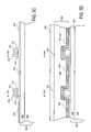
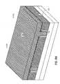
- FIG. 1illustrates a standard fully depleted silicon on insulator (SOI) transistor 100 .
- SOI transistor 100includes a single crystalline silicon substrate 102 having an insulating layer 104 , such as a buried oxide formed thereon.
- a single crystalline silicon body 106is formed on the insulating layer 104 .
- a gate dielectric layer 108is formed on the single crystalline silicon body 106 and a gate electrode 110 formed on the gate dielectric 108 .
- Source 112 and drain 114 regionsare formed in the silicon body 106 along laterally opposite sides of a polysilicon gate electrode 110 .
- the need forever decreasing silicon film thickness (Tsi)makes this approach increasingly impractical.
- the thickness required of the silicon bodyis thought to need to be less than 10 nanometers, and around 6 nanometer for a 20 nanometer gate length. The fabrication of thin silicon films with thicknesses of less than 10 nanometers, is considered to be extremely difficult.
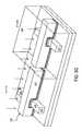
- a double gate (DG) devicesuch as shown in FIGS. 2A and 2B , have been proposed to alleviate the silicon thickness issue.
- the double gate (DG) device 200includes a silicon body 202 formed on an insulating substrate 204 .
- a gate dielectric 206is formed on two sides of the silicon body 202 and a polysilicon gate electrode 208 is formed adjacent to the gate dielectric 206 formed on the two sides of the silicon body 202 .
- a sufficiently thick insulating layer 209such as silicon nitride, electrically isolates the gate electrode 208 from the top of silicon body 202 .
- Double gate (DG) device 200essentially has two gates, one on either side of the channel of the device.
- the most manufacturable form of the double gate (DG) device 200requires that the body 202 patterning be done with photolithography that is 0.7 ⁇ smaller than that used to pattern the gate length (Lg) of the device. In order to obtain high density integrated circuits, it is generally desirable to have the most aggressive lithography occur with respect to the gate length (Lg) of the gate electrode 208 .
- silicon body 202requires a silicon body etch which can produce a silicon body 202 with an aspect ratio (height to width) of about 5:1.
- gate electrodes 100 and 200 shown in FIG. 1 and FIGS. 2A and 2Bare typically formed from a doped polycrystalline silicon film.
- Polysilicon gate electrodessuffer from the formation of charge carrier depletion regions also known as “poly depletion”. That is, when a voltage is applied to the polycrystalline gate electrode, a depletion region 120 and 220 forms in the lower part of the polycrystalline gate electrode adjacent to the gate dielectric layer 108 and 206 respectively.
- the result in affectis an increase in the electrical thickness of the gate dielectric layer. For example, in order to fabricate a transistor, such as shown in FIG. 1 , with a 90 nanometer gate length, a 14 ⁇ thick silicon oxide dielectric layer is necessary for optimal electrical performance.
- the poly depletion region 120can be on the order of 5 ⁇ thereby essentially increasing the electrical thickness (Tox) of the gate dielectric layer by 33%.
- Toxelectrical thickness
- Such an increase in the gate dielectric electrical thicknessdramatically reduces the performance of the fabricated transistor. It is to be appreciated, that as device dimensions are scaled down, in order to integrate an ever larger number of transistors into a single integrated circuit in the electrical thickness of the gate oxide layer must also be proportionally scaled down. Poly depletion effects hinder the ability to further scale down transistor dimensions.
- FIG. 1is an illustration of a cross-sectional view of a depleted substrate transistor
- FIGS. 2A and 2Billustrate a double gate depleted substrate transistor.
- FIG. 3is an illustration of a CMOS integrated circuit comprising a nonplanar n type transistor having a metal gate electrode and a nonplanar p type transistor having a metal gate electrode.
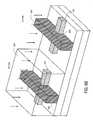
- FIG. 4Aillustrates a CMOS integrated circuit having an n type nonplanar transistor with a metal gate electrode which includes raised source and drain regions and silicided regions and a nonplanar p type transistor with a metal gate electrode and with raised source and drain regions and silicided regions.
- FIG. 4Bis an illustration of a CMOS integrated circuit having an n type nonplanar transistor with a metal gate electrode and multiple semiconductor bodies and a p type nonplanar transistor with a metal gate electrode and multiple semiconductor bodies.
- FIGS. 5A-5Lillustrate a method of fabricating a CMOS integrated circuit having a n type nonplanar transistor with a metal gate electrode and a p type nonplanar transistor with a metal gate electrode utilizing a subtractive fabrication process.
- FIGS. 6A-6Oillustrate a method of fabricating a CMOS integrated circuit comprising an n type nonplanar transistor with a metal gate electrode and a p type nonplanar transistor with a metal gate electrode utilizing a replacement gate fabrication process.
- a nonplanar transistor having a gate electrode comprising a lower metal layeris described.
- numerous specific detailsare set forth in order to provide a thorough understanding of the present invention.
- well known semiconductor processing techniques and featureshave not been described in particular detail in order to not unnecessarily obscure the present invention.
- the present inventionis a novel nonplanar transistor having a metal gate electrode.
- a nonplanar deviceincludes a semiconductor body having a top surface and laterally opposite sidewalls formed on a substrate.
- a gate dielectricis formed on the top surface and on the sidewalls of the channel region of the semiconductor body.
- a metal gate electrodeis then formed around the semiconductor body so that it covers the top surface and two sides of the semiconductor body. Since the gate electrode covers the semiconductor body on three sides the transistor essentially has three gate electrodes, one on the top of the semiconductor body and one on each of the sidewalls of the semiconductor body.
- Such a nonplanar transistorcan be referred to as a trigate transistor since it essentially has three gate electrodes.
- the nonplanar device of the present inventionhas a metal gate electrode.
- a metal gate electrodeprevents charge carrier depletion phenomenon associated with conventional polysilicon gate electrodes.
- the use of a metal gate electrodereduces the Tox or electrical thickness of the effective gate dielectric which thereby improves the electrical performance of the device.
- a nonplanar transistor with a metal gate electrode in accordance with the present inventioncan be fabricated with a subtractive approach or a replacement gate approach.
- the gate electrode material including a lower metal filmis blanket deposited over the insulating substrate and semiconductor body.
- the gate electrode materialis then patterned into a gate electrode utilizing standard photolithography and etching techniques.
- a disadvantage of the subtractive approachis that when forming both PMOS and NMOS device on the same insulating substrate, the gate electrode for each of the devices will be formed from the gate electrode material which is typically a material having a midgap work function. Utilizing a single material for both the PMOS and NMOS devices as opposed to a material tailored for the NMOS device and a material tailored for the PMOS device is a compromise in that it does not optimize the overall electrical performance of each of the devices.
- a replacement gate techniqueis utilized to form the gate electrodes.
- a replacement gate techniqueallows different metal films to be used for the gate electrodes for the PMOS and NMOS transistors.
- the PMOS devicecan have a gate electrode with a work function that is tailored for the PMOS device and the NMOS transistor can have a gate electrode with a work function tailored for the NMOS device.
- both the NMOS and PMOS electrical characteristics and performanceare optimized.
- a sacrificial gate electrode and gate dielectricis formed over the semiconductor body. Standard source and drain doping and formation techniques including sidewall spacers can then be formed. A dielectric layer is then blanket deposited over the sacrificial gate electrode and the semiconductor body.
- the dielectric layeris then polished back to expose the top surface of the gate electrode.
- the sacrificial gate electrodecan then be removed to form a trench or opening which defines where the gate electrode is to be formed.
- a metal filmis then blanket deposited over the insulating substrate and into the trench and over the semiconductor body in the trench. The metal film is then polished back to form the gate electrode for the device.
- the sacrificial gate electrode for the NMOS device and/or the PMOS deviceis altered so that one of the sacrificial gate electrode can be removed or etched away without removing the other sacrificial gate electrodes.
- the sacrificial gate electrode for one devicee.g., NMOS
- the second devicee.g., PMOS device
- the gate electrode designed for the first devicee.g., NMOS device
- the sacrificial gate electrode over the other devicei.e., PMOS device
- PMOS devicecan then be removed and replaced with a metal film tailored to the electrical characteristics desired for the PMOS device.
- NMOS and PMOS devices with different gate electrodescan be formed on the same insulating substrate and thereby enable high performance CMOS integrated circuits to be fabricated.
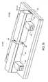
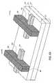
- FIG. 3shows a portion of a complimentary metal oxide semiconductor (CMOS) integrated circuit 300 which includes both an n type nonplanar transistor 310 with a metal gate electrode 320 and p type nonplanar transistor 350 with a metal gate electrode formed on an insulating substrate 302 .
- CMOScomplimentary metal oxide semiconductor
- An n type transistor 310is a field effect transistor where the carriers are electrons and a p type transistor 350 is a transistor where the carriers are holes.
- N type transistor 310 and p type transistor 350coupled together through higher levels of metallization into a functional CMOS circuit.
- n type transistor 310has a metal gate electrode 312 and p type transistor 350 has metal gate electrode 352 .
- a CMOS integrated circuit 300is shown and described with respect to FIG. 3 , the present invention is not limited to a CMOS integrated circuit and can include circuits which include only p type non-planar transistors with a metal gate electrodes or only n type nonplanar transistors with metal gate electrodes.
- CMOS integrated circuit 300can be formed on an insulating substrate 302 .
- insulating substrate 302includes a lower monocrystalline silicon substrate 304 upon which formed in insulating layer 306 , such as a silicon dioxide film.
- Integrated circuit 300can be formed on any suitable insulating substrate, such as substrates formed from silicon dioxide, nitrides, oxides, and sapphires.
- substrate 302need not necessarily be an insulating substrate can be a well known semiconductor substrate, such as but not limited to a monocrystalline silicon substrate and gallium arsenide substrate.
- N type nonplanar transistor 310includes a semiconductor body 330 formed on insulating layer 306 of insulating substrate 302 and p type nonplanar transistor 350 includes a semiconductor body 370 formed on insulating layer 306 of insulating substrate 302 .
- Semiconductor bodies 330 and 370can be formed of any well known semiconductor material, such as but not limited to silicon, germanium, silicon germanium (Si x Ge y ), gallium arsenide (GaAs), InSb, GaP, GaSb, and carbon nanotubes.
- Semiconductor bodies 330 and 370can be formed of any well know material which can be reversely altered from an insulating state to a conductive state by applying external electrical controls.
- Semiconductor bodies 330 and 370are ideally a single crystalline film when the best electrical performance of transistors 310 and 350 is desired.
- semiconductor bodies 330 and 370are single crystalline films when CMOS integrated circuit 300 is used in high performance applications, such as in high density circuits, such as a microprocessor.
- Semiconductor bodies 330 and 370can be a polycrystalline films when CMOS integrated circuit 300 is used in applications requiring less stringent performance, such as in liquid crystal displays.
- Insulating layer 306insulates semiconductor bodies 330 and 370 from the monocrystalline silicon substrate 302 .
- semiconductor bodies 330 and 370are single crystalline silicon films.
- Semiconductor body 330has a pair of laterally opposite sidewalls 331 and 332 separated by distance which defines a semiconductor body width 333 . Additionally, semiconductor body 330 has top surface 334 opposite a bottom surface 335 formed on substrate 302 . The distance between the top surface 334 and the bottom surface 335 defines the body height 336 . In an embodiment of the present invention.
- the body height 336is substantially equal to the body width 335 . In an embodiment of the present invention, the body 330 has a width 333 and a height 336 less than 30 nanometers and ideally less than 20 nanometers. In an embodiment of the present invention, the body height 336 is between one half the body width 333 to two times the body width 333 .
- semiconductor body 370has a pair of laterally opposite sidewalls 371 and 372 separated by a distance 373 which defines a semiconductor body width 373 .
- semiconductor body 370has a top surface 374 opposite a bottom surface 375 formed on substrate 302 . The distance between the top surface 374 and the bottom surface 375 defines the body height 376 .
- the body height 376is substantially equal to the body width 373 .
- the body 376is substantially equal to the body width 373 .
- the body 370has a width 373 and a height 376 less than 30 nanometers and ideally less than 20 nanometers.
- the body height 376is between one half the body width 373 to two times the body width 373 .
- N type nonplanar transistor 310has a gate dielectric layer 312 .
- Gate dielectric layer 312is formed on and around three sides of semiconductor body 330 as shown in FIG. 3 .
- Gate dielectric layer 312is formed on or adjacent to sidewall 331 , on the top surface 334 , and on or adjacent to sidewall 332 of body 330 as shown in FIG. 3 .
- nonplanar p type transistor 350has a gate dielectric layer 352 .
- Gate dielectric layer 352is formed on and around three sides of semiconductor body 370 as shown in FIG. 3 .
- Gate dielectric layer 352is formed on or adjacent to sidewall 371 , on the top surface 374 and on or adjacent to sidewall 372 of body 370 as shown in FIG. 3 .
- Gate dielectric layers 312 and 352can be formed from any well known gate dielectric films.
- the gate dielectric layersare silicon dioxide (SiO 2 ), silicon oxynitride (SiO x N y ), or a silicon nitride (Si 3 N 4 ) dielectric layer or combinations thereof.
- the gate dielectric layer 312 and 352are a silicon oxynitride film formed to a thickness between 5-20 ⁇ .
- the gate dielectric layer 312 and 352are a high K gate dielectric layer, such as a metal dielectric, such as but not limited to tantalum oxide, titanium oxide, hafnium oxide, zirconium oxide, aluminum oxide, and silicate thereof.
- dielectric layer 312 and 352can be other types of high K dielectric layers, such as but not limited to PZT and BST.
- the gate dielectric layers 312 and 352are formed of different materials and to the same thickness.
- gate dielectric layer 312is formed from a different material than the gate dielectric layer 352 and/or to a different thickness than gate dielectric layer 352 in order to provide electrical characteristics optimized for each type of transistor.
- N type nonplanar device 310has a gate electrode 320 .
- Gate electrode 320is formed on and around gate dielectric layer 312 as shown in FIG. 3 .
- Gate electrode 320is formed on or adjacent to gate dielectric layer 312 formed on sidewall 331 of semiconductor body 330 , is formed on gate dielectric layer 312 formed on the top surface 334 of semiconductor body 330 , and is formed adjacent to or on gate dielectric layer 312 formed on sidewall 332 of semiconductor body 320 .
- Gate electrode 320has a pair of laterally opposite sidewalls 322 and 324 separated by a distance which defines the gate length 326 of n type transistor 310 .
- the laterally opposite sidewalls 322 and 324 of the gate electrode 320run in a direction perpendicular to the laterally opposite sidewalls 331 and 332 of semiconductor body 330 .
- p type nonplanar device 350has a gate electrode 360 formed on and around gate dielectric layer 352 as shown in FIG. 3 .
- Gate electrode 360is formed on or adjacent to gate dielectric layer 352 formed on sidewall 371 of semiconductor body 370 , is formed on gate dielectric layer 352 formed on the top surface 374 of semiconductor body 370 and is formed adjacent to or on gate dielectric layer 352 formed on sidewall 372 of semiconductor body 370 .
- Gate electrode 370has a pair of laterally opposite sidewalls 362 and 364 separated by a distance which defines a gate length (Lg) 366 of p type transistor 350 .
- the laterally opposite sidewalls 362 and 364 of gate electrode 360run in a direction perpendicular to laterally opposite sidewalls 371 and 372 of semiconductor body 370 .
- gate electrode 320 or gate electrode 360is a metal gate electrode wherein at least the lower portion of the gate electrode formed directly adjacent to or directly on the gate dielectric layer is a metal film.
- gate electrode 320has a work function tailored for a n type device.
- gate electrode 360has a work function tailored for a p type device.
- the p type nonplanar transistor 350has a metal gate electrode selected from the group consisting of ruthenium, palladium, platinum, cobalt, nickel, and conductive metal oxides, with a workfunction between about 4.9 eV and 5.2 eV.
- the n type nonplanar transistor 310has a metal gate electrode selected from the group consisting of hafnium, zirconium, titanium, tantalum, aluminum, with a workfunction between about 3.9 eV and about 4.2 eV.
- the gate electrodewhen semiconductor body 330 of the n type device 310 is p type silicon, the gate electrode has a work function between about 3.9 eV and about 4.2 eV.
- gate electrode 360has a work function between about 4.9 eV and about 5.2 eV.
- gate electrodes 320 and 360can be a single metal film or can be a composite stack of thin films which include a lower metal film.
- gate electrodes 320 and/or 360are metal gate electrodes selected from the group consisting of tungsten, tantalum, titanium, and their nitrides.
- gate electrode 360has a work function of approximately 1.0 eV greater than work function of gate electrode 320 of the n type device.
- gate electrodes 320 and 360are formed from the same film or composite stack of films. In an embodiment of the of the present invention, gate electrodes 320 and 360 have a midgap work function or a work function between a n type device and a p type device. In an embodiment of the present invention, when the semiconductor bodies 330 and 370 are silicon bodies, gate electrodes 320 and 360 can have a midgap work function between 4.2-4.8 eV. In an embodiment of the present invention, gate electrodes 320 and 360 include a film selected from the group consisting of nitrides and carbides of titanium, halfnium and tantalum, with a workfunction between 4.2-4.8 eV.
- gate electrodes 320 and 360are formed from a composite film comprising a lower metal film and an upper polysilicon film.
- the lower metal filmis kept thin in order help in the patterning of a gate electrode during a subtractive process.
- the lower metal portion of the gate electrodes 320 and 360are formed to a thickness between 25-100 ⁇ and the upper polysilicon film is formed to a thickness between 500-3000 ⁇ .
- N type nonplanar transistor 310has a source region 340 and a drain region 342 .
- Source region 340 and drain region 342are formed in semiconductor body 308 on opposite sides of gate electrode 320 as shown in FIG. 3 .
- Source region 340 and drain region 342are formed of n type conductivity.
- source 340 and drain region 342have a n type dopant concentration between 1 ⁇ 10 19 to 1 ⁇ 10 21 atoms/cm 3 .
- Source region 340 and drain region 342can be a uniform concentration or can include subregions of different concentrations or dopant profiles, such as tip regions (e.g., source/drain extensions).
- nonplanar n type transistor 310when nonplanar n type transistor 310 is a symmetrical transistor, source region 340 and drain region 342 have the same doping concentration and profile. In an embodiment of the present invention, the nonplanar n type transistor 310 is formed as an asymmetrical transistor wherein the doping concentration profile of the source region 340 and drain region 342 may vary in order to obtain particular electrical characteristics.
- p type nonplanar transistor 350has a source region 380 and drain region 382 .
- Source region 380 and drain region 382are formed in semiconductor body 370 on opposite sides of gate electrode 360 as shown in FIG. 3 .
- the source region 380 and the drain region 382are formed of p type conductivity.
- the source region 380 and drain region 382have a p type doping concentration of between 1 ⁇ 10 19 to 1 ⁇ 10 21 atoms/cm 3 .
- Source region 380 and drain region 382can be formed of uniform concentration or can include subregions of different concentration dopants profiles, such as tip regions (e.g., source/drain regions extensions).
- nonplanar p type transistor 350when nonplanar p type transistor 350 is a symmetrical transistor, source region 380 and drain 382 have the same doping concentration and profile. In the embodiment of the present invention, when p type nonplanar transistor 350 is formed as an asymmetrical transistor, then the doping concentration profile of source region 380 and drain region 382 may vary in order to obtain particular electrical characteristics.
- the portion of semiconductor body 330 located between source region 340 and drain region 342defines a channel region 344 of the n type nonplanar transistor 310 .
- the channel region 344can also be defined as the area of the semiconductor body 330 surrounded by the gate electrode 320 .
- the portion 384 of semiconductor body 370 located between source region 380 and drain region 382defines a channel region 384 of p type nonplanar transistor 350 .
- Channel region 384can also be defined as the area of the semiconductor body 370 surrounded by gate electrode 360 .
- the source/drain regionstypically extend slightly beneath the gate electrodes through, for example, diffusion to define a channel region slightly smaller than the gate electrode length (Lg).
- the channel regions 344 and 384are intrinsic or undoped monocrystalline silicon. In an embodiment of the present invention, channel regions 344 or 384 are doped monocrystalline silicon. When channel region 344 is doped, it is typically doped to a p type conductivity level between 1 ⁇ 10 16 to 1 ⁇ 10 19 atoms/cm 3 . When channel region 384 is doped and is typically doped to a n type conductivity level between 1 ⁇ 10 16 to 1 ⁇ 10 19 atoms/cm 3 . Channel regions 344 and 384 can be uniformly doped or can be doped nonunifommly or with different concentrations to provide particular electrical performance characteristics. For example, channel regions 344 and 384 can include well known “halo” regions, if desired.
- the n type nonplanar transistor 310is characterized in having three channels and three gates, one gate (g 1 ) which extends between the source and drain regions on side 331 of semiconductor body 330 , a second (g 2 ) which extends between the source and drain regions on the top surface 334 of semiconductor body 330 , and a third (g 3 ) which extends between the source and drain regions on the sidewall 332 of semiconductor body 330 .
- nonplanar transistor 310can be referred to as a tri-gate transistor.
- the gate width (Gw) of the transistor 310is the sum of the width of the three channel regions.
- gate width of transistor 310is equal to the height 336 of semiconductor body 330 at sidewall 331 , plus the width of semiconductor body 330 at the top surface 334 , plus the height 336 of semiconductor body 330 at sidewall 332 .
- nonplanar p type transistor 350is characterized as having three channels and three gates, one channel and gate (g 1 ) which extends between the source and drain regions on side 371 of semiconductor body 370 , a second channel and gate (g 2 ) which extends between the source and drain regions on the top surface 374 of semiconductor body 370 , and a third channel and gate (g 3 ) which extends between the source and drain regions on a sidewall 372 of semiconductor body 370 .
- nonplanar transistor 350can be referred to as a tri-gate transistor.
- the gate “width” (Gw), a transistor 350is a sum of the width of the three channel regions. That is, the gate width of the transistor 350 is equal to the height 376 of semiconductor body 370 at sidewall 371 , plus the width 373 of semiconductor body 370 at the top surface 374 , plus the height 376 of the semiconductor body 370 of sidewall 372 .
- Larger width n type and p type nonplanar transistorcan be obtained by using multiple devices coupled together (e.g., multiple silicon bodies 330 surrounded by a single gate electrode 320 or multiple semiconductor bodies 370 surrounded by a single gate electrode 360 ).
- transistors 310 and 350can be operated in a fully depleted manner wherein when transistors 310 and 350 are turned “on” the channel region 350 fully depletes thereby providing the advantageous electrical characteristics and performance of a fully depleted transistor. That is, when transistors 310 and 350 are turned “ON” a depletion region is formed in the channel region along with an inversion layer at the surfaces of the channel regions 344 and 384 (i.e., an inversion layer is formed on the side surfaces and top surface of the semiconductor body).
- the inversion layerhas the same conductivity type as the source and drain regions and forms a conductive channel between the source and drain regions to allow current to flow therebetween.
- the depletion regiondepletes free carriers from beneath the inversion layer.
- the depletion regionextends to the bottom of channel regions 344 and 384 , thus the transistor can be said to be a “fully depleted” transistor.
- Fully depleted transistorshave improved electrical performance characteristics over non-fully depleted or partially depleted transistors. For example, operating transistors 310 and 350 in a fully depleted manner, gives the transistors an ideal or very steep subthreshold slope.
- Nonplanar transistors 310 and 350can be fabricated with very steep sub-threshold slope of less than 80 mV/decade, and ideally about 60 mV/decade even when fabricated with semiconductor body thicknesses of less than 30 nm.
- transistors 310 and 350have improved drain induced barrier (DIBL) lowing effect which provides for better “OFF” state leakage which results in lower leakage and thereby lower power consumption.
- DIBLdrain induced barrier
- the nonplanar transistors 310 and 350have a DIBL effect of less than 100 mV/V and ideally less than 40 mV/V. It is to be appreciated that transistor 310 and 350 need not necessarily be operated in a fully depleted manner, if desired (e.g., semiconductor bodies can be made large so they do not fully deplete).
- the transistors 310 and 350 of the present inventioncan be said to be a nonplanar transistor because the inversion layer of the channel regions 344 and 384 are formed in both the horizontal and vertical directions in semiconductor bodies 330 and 370 .
- the semiconductor device of the present inventioncan also be considered a nonplanar device because the electric field from the gate electrode 320 and 360 are applied from both horizontal (g 2 ) and vertical sides (g 1 and g 3 ).
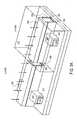
- the source and drain regions of the nonplanar transistors 310 and 350can include a silicon or other semiconductor film 410 formed on and around semiconductor body as shown in FIG. 4A .
- semiconductor film 410can be a silicon film or a silicon alloy such as silicon germanium (SixGey).
- the semiconductor film 410is a single crystalline silicon film formed of the same conductivity type as the source region and drain region.
- the semiconductor filmcan be a silicon alloy such as silicon germanium where silicon comprises approximately 1 to 99 atomic percent of the alloy.
- the semiconductor film 410need not necessarily be a single crystalline semiconductor film and in an embodiment can be a polycrystalline film.
- the semiconductor film 410is formed on the source region and on the drain region of semiconductor body to form “raised” source and drain regions.
- Semiconductor film 410can be electrically isolated from the gate electrode by a pair of dielectric sidewall spacers 420 such as silicon nitride or silicon oxide or composites thereof.
- Sidewall spacers 420run along the laterally opposite sidewalls of gate electrodes 320 and 360 as shown in FIG. 4A thereby isolating the semiconductor film 410 from gate electrode as shown in FIG. 4A .
- An embodiment of the present invention sidewalls spacers 420have a thickness of between 20-200 ⁇ .
- the thickness of the source and drain regionsis increased thereby reducing the source/drain contact resistance to transistors 310 and 350 and improving their electrical characteristics and performance.
- a silicide film 430such as, but not limited to, titanium silicide, nickel silicide, and cobalt silicide is formed on the source region and drain regions.
- silicide film 430is formed on a silicon film 410 on silicon body 330 and silicon body 370 as shown in FIG. 4A .
- Silicide film 430can also be formed directly onto silicon bodies 330 and 370 .
- silicide film 430can be formed on silicon bodies 330 and 370 by first forming a silicon film such as an undoped silicon film on silicon bodies 330 and 370 and then completely consuming the silicon film during the silicide process.
- Dielectric spacers 420enables silicide film 430 to be formed on semiconductor bodies 330 and 370 or on silicon film 410 in a self-aligned process (i.e., a salicide process).
- a semiconductor or silicon film 440can also be formed on the top of gate electrodes 320 and 360 as can a silicide film 450 on the top surface gate electrodes 320 and 360 when the top portion of the gate electrode is a silicon or semiconductor film.
- Silicide film 450 and silicon film 440are typically formed at the same time as silicide film 430 and silicon film 420 on silicon bodies 330 and 370 .
- the formation of a silicon film 440 and a silicide film 450 on the gate electrodecan reduce the contact resistance to the gate thereby improving the electrical performance of transistor 300 .
- transistors 310 and 350are equal to the sum of the three gate width created from semiconductor bodies 330 and 370 respectively.
- transistors 310 and 350can include an additional or multiple semiconductor bodies or fingers 330 and 370 as shown in FIG. 4B .
- Each semiconductor body 330 and 370has a gate dielectric layer 312 and 352 formed on its top surface and sidewalls as shown in FIG. 4B .
- Gate electrode 320 and 360is formed on and adjacent to each gate dielectric 312 and 352 on each of the semiconductor bodies 330 and 370 as shown in FIG. 4B .
- Each semiconductor body 330also includes a source region 340 and drain region 342 formed in each semiconductor body 330 on opposite sides of gate electrode 320 as shown in FIG. 4B .
- each semiconductor body 370also includes a source region 380 and drain region 382 formed in each semiconductor body 370 on opposite sides of gate electrode 360 as shown in FIG. 4B .
- each semiconductor body 330is formed with the same width and height (thickness) as the other semiconductor bodies 330 .
- each semiconductor body 370is formed with the same width and height (thickness) as the other semiconductor bodies 370 .
- each source region 340 and drain region 342 of the semiconductor body 330are electrically coupled together by the doped semiconductor material used to form semiconductor body 340 to form a source landing pad 460 and a drain landing pad 480 as shown in FIG. 4B .
- each source region 380 and drain region 382 of the semiconductor body 370are electrically coupled together by the doped semiconductor material used to form semiconductor body 380 to form a source landing pad 460 and a drain landing pad 480 as shown in FIG. 4B .
- the landing pads 460 and 480are doped to the same conductivity type and levels as the source and drain regions are for each of the transistors 310 and 350 .
- the source region 340 and drain regions 342can be coupled together by higher levels of metallization (e.g., metal 1 , metal 2 , metal 3 . . . ) used to electrically interconnect various transistors 310 and 350 together into functional circuits.
- the source region 380 and drain regions 382can be coupled together by higher levels of metallization (e.g., metal 1 , metal 2 , metal 3 . . . ) used to electrically interconnect various transistors 310 and 350 together into functional circuits.
- the nonplanar transistors 310 and 350can be formed with any gate width desired.
- FIG. 5A-5LA method of forming a complimentary metal oxide semiconductor integrated circuit having a n type nonplanar transistor with a metal gate electrode and a p type nonplanar transistor with a metal gate electrode utilizing a subtractive fabrication process is illustrated in FIG. 5A-5L .
- a process for forming a CMOS integrated circuitis illustrated in FIGS. 5A-5L , it is to be appreciated that one need not necessarily form a CMOS integrated circuit and one can form an integrated circuit comprising only n type nonplanar devices with a metal gate electrodes or p type nonplanar devices with metal gate electrodes, if desired. In such a case, the processing steps to fabricate the unused transistor type are eliminated.
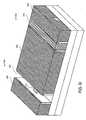
- CMOS integrated circuitbegins with a substrate 502 .
- a silicon or semiconductor film 508is formed on substrate 502 as shown in FIG. 5A .
- the substrate 502is an insulating substrate, such as shown in FIG. 5A .
- insulating substrate 502includes a lower monocrystalline silicon substrate 504 and a top insulating layer 506 , such as silicon dioxide film or a silicon nitride film. Insulating layer 506 isolates semiconductor film 508 from substrate 504 and in an embodiment is formed to a thickness between 200-2000 ⁇ . Insulating layer 506 is sometimes referred to as a “buried oxide” layer.
- a silicon or semiconductor on insulating (SOI) substrate 500is created.
- SOIsemiconductor on insulator
- the present inventioncan be also carried out on standard semiconductor substrates, such as but not limited to monocrystalline silicon substrates and gallium arsenide substrates.
- semiconductor film 508is ideally a silicon film, in other embodiments it can be other types of semiconductor films, such as but not limited to germanium (Ge), a silicon germanium alloy (SixGey), gallium arsenide (GaAs), InSb, GaP, GaSb, as well as carbon nanotubes.
- semiconductor film 508is an intrinsic (i.e., undoped) silicon film.
- the semiconductor film 508is doped to a p type conductivity at locations 505 where n type transistors are desired and is doped to a n type conductivity at locations 503 where a p type transistor is desired.
- Semiconductor film 508would typically be doped to a p type or n type conductivity with a concentration level of between 1 ⁇ 10 16 to 1 ⁇ 10 19 atoms/cm 3 .
- P type regions 505 and n type regions 503can be formed in semiconductor film 508 utilizing well known photolithography masking and ion implantation techniques.
- Semiconductor film 508is formed to a thickness 509 which is approximately equal to the height desired for the subsequently formed semiconductor body or bodies of the fabricated nonplanar transistor. In an embodiment of the present invention, semiconductor film 508 has a thickness or height 509 of less than 30 nanometers and ideally less than 20 nanometers. In an embodiment of the present invention, semiconductor film 508 is formed to the thickness approximately equal to the gate “length” desired of the fabricated nonplanar transistor. In an embodiment of the present invention, semiconductor film 508 is formed thicker than desired gate length of the device. In an embodiment of the present invention, semiconductor film 580 is formed to a thickness which will enable the fabricated nonplanar transistor to be operated in a fully depleted manner for its designed gate length (Lg).
- Lggate length
- Semiconductor film 508can be formed on insulating substrate 502 in any well-known method.
- a silicon on insulator substrateknown as the SIMOX technique
- oxygen atomsare implanted at a high dose into a single crystalline silicon substrate and then anneal to form the buried oxide 506 within the substrate.
- the portion of the single crystalline silicon substrate above the buried oxidebecomes the silicon film 508 .
- Another technique currently used to form SOI substratesis an epitaxial silicon film transfer technique which is generally referred to as bonded SOI.
- bonded SOIIn this technique a first silicon wafer has a thin oxide grown on its surface that will later serve as the buried oxide 506 in the SOI structure.
- a high dose hydrogen implantis made into the first silicon wafer to form a high stress region below the silicon surface of the first wafer.
- This first waferis then flipped over and bonded to the surface of a second silicon wafer.
- the first waferis then cleaved along the high stress plane created by the hydrogen implant. This results in a SOI structure with a thin silicon layer on top, the buried oxide underneath all on top of the single crystalline silicon substrate.
- Well-known smoothing techniquessuch as HCl smoothing or chemical mechanical polishing (CMP) can be used to smooth the top surface of semiconductor film 508 to its desired thickness.
- isolation regionscan be formed into SOI substrate 500 in order to isolate the various transistors to be formed therein from one another. Isolation regions can be formed by etching away portions of the substrate film 508 surrounding a nonplanar transistor, by for example well-known photolithographic and etching techniques, and then back filling the etched regions with an insulating film, such as SiO 2 . Alternatively, isolation regions can be formed prior to forming the n type and/or p type doped regions 503 and 505 respectively.
- a semiconductor body 510 for the n type deviceis formed from the p type region 505 of semiconductor film 508 and a semiconductor body 512 for the p type device is formed from the n type region 503 of the semiconductor film 508 as shown in FIG. 5B .
- each device typemay contain multiple semiconductor bodies 510 or 512 as illustrated in FIG. 4B .
- source/drain landing padsare not shown in FIG. 5B , source/drain landing pads can be formed at this time in order to connect together various source regions and to connect together various drain regions of the fabricated transistor.
- Semiconductor bodies 510 and 512can be formed by well known photolithography and etching techniques.
- a photoresist filmis blanket deposited over semiconductor film 508 .
- the photoresist maskis then patterned into a photoresist mask utilizing well known masking, exposing and developing techniques to define the locations where the semiconductor bodies or fins are desired (and landing pads, if used).
- the semiconductor film 508is then etched in alignment with the photoresist mask to form the semiconductor bodies 510 and 512 (and source/drain landing pads if desired) as shown in FIG. 5B .
- the semiconductor body 508is etched until the underlying buried oxide layer 506 is exposed.
- the semiconductor bodies 510 and 512have a width 514 which is equal to or greater than the width desired for the gate length (Lg) of the fabricated transistor. In this way, the most stringent photolithography constraints used to fabricate the transistor are associated with the gate electrode patterning and not the semiconductor body of fin definition.
- the semiconductor bodies or fins 510 and 512have a width 514 less than or equal to 30 nanometers and ideally less than or equal to 20 nanometers.
- the semiconductor bodies or fins 510 and 512have a width 514 approximately equal to the semiconductor body height 509 . In an embodiment of the present invention, the semiconductor bodies 510 and 512 have a width 514 which is between one half the semiconductor body height 509 and two times the semiconductor body height 509 . It is to be appreciated that, if desired, semiconductor bodies 510 and 512 need not necessarily be formed to the same width.
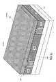
- a gate dielectric layer 516is formed on and around semiconductor body 510 and semiconductor body 512 . That is, a gate dielectric layer 516 is formed on the top surface 515 of semiconductor body 510 as well on the laterally opposite sidewalls 513 of semiconductor body 510 . Additionally, the gate dielectric layer 516 is formed on the top surface 519 as well on the laterally opposite sidewalls 517 of semiconductor body 512 as shown in FIG. 5C .
- the gate dielectric layercan be a deposited or grown dielectric layer.
- the gate dielectric layer 516is a silicon dioxide dielectric film grown with a dry/wet oxidation process.
- a silicon oxide filmis grown to a thickness of between 5-50 ⁇ .
- the gate dielectric layer 516is a deposited dielectric, such as but not limited to a high dielectric constant film, such as a metal oxide dielectric, such as tantalum pentaoxide (Ta 2 O 5 ) and titanium oxide (TiO 2 ), tantalum oxide, hafnium oxide, zirconium oxide, aluminum oxide, and silicate thereof or other high K dielectrics, such as PZT and BST.
- a high dielectric constant filmcan be formed by any well known technique, such as but not limited to chemical vapor deposition (CVD) or atomic layer deposition (ALD).
- CVDchemical vapor deposition
- ALDatomic layer deposition
- a gate electrode film 520is blanket deposited over the substrate shown in FIG. 5C .
- the gate electrode film 520is used to form the gate electrodes for the n type and p type nonplanar transistors.
- the gate electrode film 520includes at least a lower metal layer formed directly on or adjacent to the gate dielectric layer 516 .
- Gate electrode film 520can be a single metal film or can be a composite film formed of multiple layers.
- the gate electrode film 520produces a midgap work function between a n type device and a p type device.
- the gate electrode film 520produces a work function between 4.2-4.8 eV.
- the gate electrode film 520comprises a composite stack which includes a lower metal layer 522 formed in direct contact with the gate dielectric layer 516 and an upper silicon or silicon alloy film 524 , such as polycrystalline silicon or silicon germanium.
- a composite polycrystalline silicon/metal filmis utilized where the upper polycrystalline silicon film is formed significantly thicker than the lower metal film, such as for example, 5-30 times thicker. Such as thickness ratio aids in the subsequent anisotropic etching of the gate electrode material 520 to form a gate electrode with vertical sidewalls which enable minimum dimension gate lengths to be achieved.
- the gate electrodehas a lower metal film between 25-100 ⁇ thick and an upper metal film between 500-3000 ⁇ thick.
- the lower metal filmis a metal selected from the group consisting of the nitrides and carbides of titanium, halfnium and tantalum, with a work function that is between 4.2-4.8 eV.
- the gate electrode film 520can be formed by any well known method, such as but not limited to chemical vapor deposition (CVD) and sputtering.
- the gate electrode material 520is deposited to a thickness or height of at least three times the height of the semiconductor bodies 510 and 512 .
- the gate electrode material 520is formed to a thickness between 200-3000 ⁇ .
- the gate electrode material 520can be planarized by, for example, chemical mechanical planarization in order to form a gate electrode film 520 with a smooth top surface 525 .
- a smooth top surfacewill aid in the subsequent patterning of the gate electrode.
- a hard mask film 526such as but not limited to silicon nitride of silicon oxynitride, can be blanket deposited over the gate electrode material 520 as shown in FIG. 5D .
- the hard mask layer 526helps improve the anisotropic patterning of the gate electrode material 520 .
- the hard mask layer 526can be used as a mask to prevent the channel doping during the subsequent formation of the source and drain regions. This is especially important when the gate electrode material 520 comprises a single metal layer or multiple metal layers which are unable to block ions during ion implantation to form the source and drain regions.
- the gate electrode material 520is patterned into gate electrodes as shown in FIG. 5E .
- the gate electrode material 520is patterned into a gate electrode 526 for the n type transistor and gate electrode 528 for the p type transistor.
- Well known photolithography and etching techniquescan be used to pattern the gate electrode material 520 into a gate electrode 526 and 528 .
- a photoresist materialcan be blanket deposited over the gate electrode material 520 . Photolithography techniques, such as masking, exposing and developing can then be used to pattern the photoresist material into photoresist mask which defines the location where electrodes 526 and 528 are desired.
- the photolithography process used to define the gate electrodesutilizes the minimum or smallest dimension lithography process used to fabricate the nonplanar transistors.
- the hard mask layer 526is etched in alignment with the photoresist mask to form the hard mask 527 .
- the hard mask materialcan be patterned with any technique well known in the industry such as utilizing a reactive ion etching.
- the polysilicon film 524is etched in alignment with the photoresist mask and/or hard mask 527 .
- the hard maskis formed of a material which does not significantly etch or erode during the polysilicon or bulk etch, so that the fidelity between a pattern formed in the hard mask is continued into the polysilicon layer 524 during the polysilicon etch. It is to be appreciated that the polysilicon etch can erode the photoresist mask and cause inaccurate etching of the polysilicon film if a hard mask is not utilized.
- the polysilicon etchis continued until the underlying metal film 522 is reached.
- the etch chemistryis then switched to an etchant which can etch the lower metal film 522 .
- the lower metal film 522is titanium carbide an etch chemistry of comprising HBr and C 12 can be utilized.
- the lower metal film 522is etched utilizing a wet etchant.
- Wet etchantsare isotropic in nature and therefore require a very thin lower metal film 522 in order to etch the lower metal film without dramatically under cutting the polysilicon film 524 .
- the lower metal filmis titanium nitride and it is wet etched with a chemistry comprising sulfuric acid and hydrogen peroxide. The end result is a formation of gate electrodes 526 and 528 having nearly vertical sidewalls and formed to the minimum dimension (critical dimension) allowable by the photolithography process to produce minimum gate length (Lg) gate electrodes.
- the source and drain regions of the p type and n type transistorsare formed in the semiconductor bodies 510 and 512 respectively.
- the n type and p type transistorsinclude tip or source/drain extensions.
- a photoresist mask 530can be formed over the n type transistor and the p type transistor region left masked or exposed as shown in FIG. 5F .
- dopantsare placed within the exposed portions of the semiconductor body 512 which are not covered by gate electrode 528 .
- the semiconductor body 512is doped in alignment with the outside edges of the gate electrode 528 to p type conductivity, with for example boron, to a concentration between 1 ⁇ 10 20 to 1 ⁇ 10 21 atoms/cm 3 .
- the semiconductor film 512is doped by ion-implantation.
- the ion-implantationoccurs in a vertical direction (i.e., perpendicular to the substrate) as shown in FIG. 5F .
- the photoresist mask 530prevents the n type device from being implanted with p type dopants.
- the gate electrodecomprises a upper polysilicon film 524 it can be doped during the ion-implantation process.
- Gate electrode 528acts as a mask to prevent the ion-implantation step from doping the channel region 532 of the p type transistor.
- the channel region 532is a portion of the semiconductor body 512 located beneath or surrounded by gate electrode 528 . If gate electrode 528 is entirely a metal electrode, the dielectric hard mask 527 can be left on the gate electrode 528 during the ion implantation step in order to mask the channel 532 and prevent the channel region 532 from being doped during the ion-implantation process. It is to be appreciated that other methods, such as solid source diffusion may be used to dope the semiconductor body 512 to form the tip regions 534 , if desired.
- the photoresist mask 530is removed with well known techniques.
- n type source/drain tip region, tip or extension regions 536can be formed in semiconductor body 510 on opposite sides of gate electrode 526 .
- a photoresist mask 538can be formed over the region of the substrate containing the p type device and the n type region left unmasked as shown in FIG. 5G .
- n type dopantssuch as arsenic or phosphorous, can be ion-implanted into the semiconductor body 510 to form the source/drain extensions 536 .
- Photoresist mask 538prevents the p type device from being implanted with n type dopants.
- the semiconductor body 510can be doped with n type conductivity ions to a concentration between 1 ⁇ 10 21 to 1 ⁇ 10 21 atoms/cm 3 .
- the ion implantationoccurs in a vertical direction (i.e., in a direction perpendicular to substrate 500 ) as shown in FIG. 5G .
- the gate electrodeincludes an upper polysilicon film 524 it can also be doped at this time also.
- Gate electrode 526prevents the channel region of the n type device from becoming implanted with n type impurities. When gate electrode 526 comprises only a metal or multiple metal layers hard mask 527 can be left on to prevent the doping of the channel region.
- the photoresist mask 538is removed with well known techniques.
- (halo) regionscan be formed in the semiconductor bodies 510 and 512 prior to the formation of the source/drain regions or source/drain extension regions.
- Halo regionsare doped regions formed in the channel regions 538 and 532 of the device and are of the conductivity but of slightly higher concentration than the dopant of the channel region of the device.
- Halo regionscan be formed by ion implanting dopants beneath the gate electrodes 526 and 528 utilizing large angled ion implantation techniques.
- the substrate shown in FIG. 5Gcan be further processed to form additional features, such as heavily doped source/drain contact regions, deposited silicon on the source and drain regions as well as the gate electrode and the formation of silicide on the source and drain contact regions as well as the gate electrode, if desired.
- dielectric sidewalls spacer 540can be formed on the sidewalls of gate electrodes 526 and 528 as shown in FIG. 5H .
- Spacers 540can be utilized to offset heavy source/drain contact implants and can be used to isolate source/drain regions from the gate electrode during a selective silicon deposition process and can be used in a salicide process to form silicide on the source and drain regions as well as on the top of the gate electrode, if desired.
- Spacers 540can be formed by blanket depositing a conformal dielectric film, such as but not limited to silicon nitride, silicon oxide, silicon oxynitride or combination thereof over the substrate including the gate electrodes 526 and 528 and semiconductor bodies 510 and 512 .
- the dielectric filmis deposited in conformal manner so that it forms to substantially equal heights on vertical surfaces, such as the sidewalls of the gate electrodes 526 and 528 , as well as on horizontal surfaces, such as in the top of the semiconductor bodies and the top of the gate electrode 526 and 528 .
- the dielectric filmis a silicon nitride film formed by a hot wall, low pressure chemical vapor deposition (LPCVD) process.
- LPCVDlow pressure chemical vapor deposition
- the deposited thickness of the dielectric filmdetermines the width or thickness of the formed spacers.
- the dielectric filmis formed to a thickness between 20-200 ⁇ .
- the dielectric filmis anisotropically etched by, for example, plasma etching or reactive ion etching to form the sidewall spacers 540 .
- the anisotropic etch of the dielectric filmremoves the dielectric film from horizontal surfaces, such as top of gate electrodes 526 and 528 and leaves dielectric sidewalls spacers 540 adjacent to the vertical surfaces, such as the sidewalls of gate electrodes 526 and 528 .
- the etchis continued for sufficient period of time to remove the dielectric film from all horizontal surfaces.
- an over etchis utilized so that the spacer material on the sidewalls of the semiconductor body 510 and 512 is removed as shown in FIG. 5H .
- the resultis the formation of sidewall spacers 540 which run along and adjacent to the sidewalls of gate electrodes 526 and 528 as shown in FIG. 5H .
- a semiconductor film 542can be formed on the exposed surfaces of semiconductor body 510 and 520 (as well as on landing pads, if used) as shown in FIG. 5 . Additionally, if desired, semiconductor film 542 can be formed on the top of the gate electrodes 526 and 528 , if desired.
- the semiconductor filmcan be a single crystalline film or a polycrystalline film.
- the semiconductor film 542is an epitaxial or (single crystalline) silicon film.
- the silicon film 542is formed by a selective deposition process whereby silicon is formed only on exposed regions which contain silicon, such as the exposed top surface and sidewalls of silicon bodies 510 and 512 .
- a silicon filmdoes not form on dielectric areas, such as sidewall spacers 540 .
- gate electrode 526 and 528include a top polycrystalline silicon film
- siliconcan also be selectively formed on the top surface of the gate electrode to form a silicon film 542 thereon.
- a silicon film 542is formed to a thickness between 50-500 ⁇ .
- the silicon filmis formed to a thickness sufficient to provide enough silicon to be used or consumed during the formation of a silicide film on the source and drain regions.
- the deposited silicon film 542is an intrinsic silicon film (i.e., an undoped silicon film).
- a semiconductor film 542creates raised source and drain regions which improves the parasitics of the transistors.
- the deposited silicon film 542is doped to the conductivity and density desired for the source and drain contact regions.
- a photoresist mask 544is formed over the region of the substrate for the n type device and the p type device left unmasked.
- an ion implantation stepis utilized to implant p type conductivity ions, such as boron, into the deposited semiconductor film 542 as well as into the semiconductor body 512 to form heavily doped source/drain regions.
- the ion implantation processcan dope the deposited silicon film 542 and the silicon body 512 located underneath to a p type conductivity type with a concentration between 1 ⁇ 10 20 to 1 ⁇ 10 20 atoms/cm 3 to form a source contact region 546 and a drain contact region 548 .
- Sidewall spacers 540offset the heavy source/drain implantation step and define the tip regions as the regions of the doped semiconductor body 512 beneath sidewall spacers 540 .
- the above referenced processform a source region and a drain region which each comprise a tip region 534 and a contact regions 546 and 548 .
- the tip region 534is a region of the semiconductor body 512 located beneath the sidewall spacers 540 .
- the contact regions 546 and 548are the region of the semiconductor body and deposited silicon film which are adjacent to the outside edge of the sidewall spacers 540 . Photoresist mask 544 can then removed.
- a photoresist mask 550is formed over the p type region of the substrate and the n type region left unmasked.
- n type conductivity ionssuch as arsenic and phosphorous, are ion implanted into the semiconductor film 546 as well as into the semiconductor body 510 located beneath.
- the ion implantation processdopes the deposited silicon film 542 and the silicon body 512 located underneath to a concentration between 1 ⁇ 10 20 to 1 ⁇ 10 21 atoms/cm 3 to form a source contact regions 552 and a drain contact region 554 .
- the sidewall spacers 540offset the n type source/drain contact implantation step and define the n type tip regions 536 as a region of the doped semiconductor body 510 located beneath sidewall spacers 540 .
- the photoresist mask 554can be removed.
- the implanted dopants which from the tip regions 536 and 534 and the source/drain contacts regionsare not yet activated. That is, they have been implanted into the semiconductor material but sit in interstitial sites and have not yet been incorporated into the semiconductor or silicon crystal lattice.
- a high temperature annealis required to activate the dopants.
- the dopantsare activated with a rapid thermal anneal process at a temperature between 600-1100° C. for a time between 1-60 seconds in a atmosphere comprising argon and nitrogen.
- the source/drain dopantscan be activated by the anneal used to subsequently form silicide on the transistor as described below.
- a refractory metal silicide layer 560can be formed on the source and drain contact regions of a p and n type device as well as on the top of the gate electrode 526 and 528 , if desired.
- a refractory metal silicide film 560can be formed with a self-aligned process, such as a silicide process.
- a refractory metal filmsuch titanium, tungsten, nickel, colbalt or alike are blanket deposited over the substrate and silicon films formed on the semiconductor bodies 510 and 512 and gate electrode 526 and 528 .
- the substrateis then heated to a suitable temperature to cause a refractory metal film to react with silicon portions of the substrate, such as silicon film 542 formed on semiconductor bodies 510 and 512 and semiconductor film 542 formed on the gate electrodes in order to form a refractory metal silicide 560 .
- silicon portions of the substratesuch as silicon film 542 formed on semiconductor bodies 510 and 512 and semiconductor film 542 formed on the gate electrodes in order to form a refractory metal silicide 560 .
- Locations where silicon is unavailable to reactsuch as dielectric spacers 540 and exposed portions of buried oxide 506 do not react and remain as refractory metal.
- selective etchsuch as a wet etch, can then be utilized to remove the unreacted refractory metal and leave refractory metal silicide 560 on the contact areas. In this way, metal silicide films can be self-aligned to the contact regions of the nonplanar transistors. This completes fabrication of the n type and p type nonplanar
- FIGS. 6A-6Oillustrate a method of forming a p type nonplanar device with a metal gate electrode and a n type nonplanar device with a metal gate electrode utilizing a replacement gate technique.
- the replacement gate techniqueenables the gate electrodes for the p type device and the n type device to be formed of different materials.
- the gate electrode for the p type devicecan have a work function tailored for the p type device and the gate electrode for the n type device can have a work function tailored for the n type device.
- the performance of the CMOS integrated circuitcan be dramatically improved.
- the replacement gate processbegins with the formation of a semiconductor body or bodies 510 for the n type device and a semiconductor body or bodies 512 for the p type device as discussed above.
- a sacrificial gate dielectric layer 602 and a sacrificial gate electrode 604are formed over the top surface and sidewalls of the silicon bodies 510 and 512 as shown in FIG. 6A .
- the sacrificial gate dielectric 602is ideally formed from a material which will not sufficiently etch during the removal or etching of the sacrificial gate electrode material so that it can protect the underlying semiconductor body when the sacrificial gate electrode is subsequently removed. This is especially important when the sacrificial gate electrode material and semiconductor body are formed from the same material, such as silicon.
- the sacrificial gate dielectricis an oxide, such as silicon dioxide formed to a thickness between 10-30 ⁇ . If the sacrificial gate dielectric is a grown dielectric it will form only on the exposed surfaces of the semiconductor body 510 and not on the insulating substrate 502 . If the sacrificial gate dielectric is a deposited film it will be blanket deposited onto the insulating substrate 502 as well as the semiconductor bodies 510 and 512 .
- a sacrificial gate electrode materialis blanket deposited over the sacrificial gate dielectric, the sacrificial gate electrode material is deposited to a thickness desired for the height of the subsequently formed gate electrodes for the nonplanar devices.
- the sacrificial gate electrode material and the sacrificial gate dielectricare then patterned by well known techniques, such as photolithography and etching to form the sacrificial gate electrode 604 for the n type device and the sacrificial gate electrode 606 for the p type device as shown in FIG. 6A .
- the sacrificial gate electrode 604 and 606are patterned into the same shape and at the same location where the subsequently formed gate electrodes for the p type device and the n type device are desired.
- the sacrificial gate electrode materialis a material which can be altered into an altered sacrificial material so that either the sacrificial material or the altered sacrificial material can be selectively etched or removed without etching or removing the other. That is, the sacrificial gate electrode material is formed of a material which can be altered so that either: 1) the altered sacrificial material can be etched or removed without etching the unaltered sacrificial material or 2) the unaltered sacrificial material can be removed of etched away without etching or removing the altered sacrificial material.
- this differentiating of the p type sacrificial gate electrode and n type sacrificial gate electrodewill enable the different sacrificial gate electrodes to be removed at separate times enabling the openings to be subsequent filled with different materials.
- the sacrificial materialis a material having a crystalline structure, such as a polycrystalline film or single crystalline film which can be altered by increasing the activation energy necessary to etch the film.
- the sacrificial filmis crystalline film which can be altered by changing the crystal lattice so that altered crystal lattice has a sufficiently different activation energy than the unaltered crystal lattice.
- the sacrificial materialis crystalline film which is altered by substituting dopant atoms with atoms in the crystal lattice in the film to thereby form an altered crystal lattice which has a higher activation energy than the unaltered crystal lattice.
- dopantsare placed in the crystal lattice to alter the sacrificial film and give it a higher activation barrier than does the unaltered sacrificial film.
- an etchantwhich has an sufficiently high activation energy to etch away the unaltered film but not a high enough activation energy to etch the altered film, will only etch the unaltered film and will not etch the altered film.
- an embodiment of the present inventionutilizes a sacrificial material which can be altered to create a sufficiently different lattice energy so that the difference can be exploited to selectively remove of one without the other.
- the difference between the activation energy of the sacrificial gate electrode over the n type region and the altered sacrificial gate electrode over the p type regionis sufficient to enable the etching of one without the etching of the other.
- the sacrificial gate electrode material for the p type device and the sacrificial gate electrode material for the n type deviceare both altered, but are altered in such a manner that a difference between the altered films is sufficient to enable a selective etching one over the other.
- the sacrificial filmis a polycrystalline silicon film.
- the sacrificial filmis monocrystalline silicon film or an epitaxial silicon film.
- the polycrystalline silicon sacrificial gate electrode materialis altered by substituting boron atoms for silicon atoms in the crystal lattice.
- tip or source/drain extensionscan be formed by doping the semiconductor bodies 510 and 512 on opposites sides of the sacrificial gate electrodes 604 and 606 with impurities of the same conductivity type to be used to form the source and drain regions.
- the tip regionsare formed utilizing well known ion implantation techniques.
- a photoresist mask 608can be formed over the regions for the n type device and the region for the p type device left unmasked. P type impurities can then be ion implanted into the semiconductor body 512 in alignment with the outside edges of the sacrificial gate electrode 606 for the p type device.
- the sacrificial gate electrode 606prevents the channel region 609 of the semiconductor body 512 from being doped with p type dopants during the tip formation step.
- the sacrificial gate electrodebecomes doped with p type dopants this at this time.
- the implantation processplaces p type dopants, such as boron, into the sacrificial gate electrode 606 .
- the dopantshave not yet been activated at this time by a high temperature process, the dopants atoms reside at interstitial sites of the lattice, and are not yet substituted with atoms in the lattice.
- semiconductor body 512 and sacrificial gate electrode 606when semiconductor body 512 and sacrificial gate electrode 606 are silicon, they can be doped with boron ions at does and with energies well known in the art to subsequently form a boron concentration between 1 ⁇ 10 19 to 1 ⁇ 10 21 atoms/cm 3 .
- Photoresist mask 608prevents the n type device from being doped with p type conductivity ions.
- the photoresist mask 608is removed and a photoresist mask 610 formed over the p type device and the n type device left unmasked.
- n type impurity ionsare implanted into the semiconductor body 510 on opposite sides of the sacrificial gate electrode 604 .
- Sacrificial gate electrode 604prevents the channel region 611 of a semiconductor body 510 from being doped during the tip formation step.
- the sacrificial gate electrodealso becomes doped at this time with n type dopants.
- the dopantsreside at intersitial sites in the lattices of the sacrificial gate electrode 604 and the semiconductor body 510 , and have not yet substituted with atoms in the lattice.
- semiconductor body 510 and sacrificial gate electrode 604are silicon
- arsenic or phosphorous atomscan be implanted at a dose with an energy well known in the art to create n type concentration of between 1 ⁇ 10 19 to 1 ⁇ 10 21 atoms/cm 3 .
- the photoresist mask 610is then removed.
- dielectric sidewall spacers 612can be formed along opposite sidewalls of the sacrificial gate electrodes 604 and 606 as shown in FIG. 6D .
- the sidewall spacerscan be formed by any well known techniques, such as by blanket depositing the conformal sidewall spacer dielectric over the substrate including the top surface and sidewalls of the sacrificial gate electrodes 604 and 606 as well as on the top surface and sidewalls of semiconductor bodies 510 and 512 as well as onto the exposed surface of the insulating substrate.
- the dielectric spacer materialis deposited to a thickness which is approximately equal to the width desired for spacers 612 .
- the dielectric spacer materialis deposited to a thickness between 20-200 ⁇ .
- the spacer materialcan be a dielectric, such as silicon nitride, silicon oxide, silicon oxynitride or combinations thereof.
- the spacer materialis silicon nitride formed by a hot wall low-pressure chemical vapor deposition (LPCVD) process.
- the dielectric spacer materialis then anisotropically etched back to remove the dielectric spacer material from a horizontal surface (e.g., top surface) of the sacrificial gate electrodes 604 and 606 and the top surface of semiconductor bodies 510 and 512 and insulating substrate 602 , while leaving spacer material on the vertical surfaces (e.g., sidewalls) of sacrificial gate electrodes 604 and 606 to form sidewall spacers 612 as shown in FIG. 6D .
- the thickness of the height of the semiconductor bodies 510 and 512 and over (etch) of the anisotropic etch backcan be used to remove the spacer materials from the sidewalls of the semiconductor bodies 510 and 512 while leaving sufficient spacer material to provide spacer 612 on the sidewalls of the sacrificial gate electrodes 604 and 606 .
- additional siliconcan be formed onto the exposed top surface and sidewalls of the semiconductor bodies 510 and 512 in order to form raised source and drain regions.
- the additional siliconsuch as epitaxial silicon
- a selective silicon deposition processwill deposit silicon, such as epitaxial silicon onto silicon containing regions, such as silicon bodies 510 and 512 and will not deposit silicon onto non-silicon containing areas, such as sidewall spacers 612 .
- heavy source/drain contact regionsmay be formed in the semiconductor bodies 510 and 512 on opposite sides of the sacrificial gate electrodes 604 and 606 .
- the heavy source/drain regionsare formed by ion implantation.
- a photoresist mask 614can be formed over the n type transistor region and the p type transistor region left unmasked.
- P type dopantsare then ion implanted into the semiconductor body 512 in alignment with opposite side of sacrificial gate electrode 606 .
- the ion implantation processimplants p type dopants, into the sacrificial gate electrode 606 .
- the semiconductor body 512is silicon and the sacrificial gate electrode is polycrystalline silicon
- boron ionscan be implanted at a dose and at an energy well known in the art to subsequently form a boron concentration between 1 ⁇ 10 19 to 1 ⁇ 10 21 atoms/cm 3 in the polycrystalline silicon sacrificial gate electrode 606 and silicon body 512 .
- the dopantshave not yet been activated at this time by a high temperature process, the dopants reside at interstitial sites in the lattice, and have not yet substituted with atoms in the lattice.
- the sacrificial gate electrode 606masks the channel region 609 of the p type device from being doped with p type impurities during the heavy source/drain implant. Additionally, the sidewall spacers 612 prevent the underlying previously formed tip regions in the semiconductor body 512 from being doped by the heavy source/drain implant.
- n type conductivity ionsare ion implanted into the semiconductor body 510 on opposite sides of sacrificial gate electrode 604 in order to form heavily doped source and drain regions.
- the sacrificial gate electrode 604masks the channel region of the n type device from being doped during the heavy source/drain formation step. Additionally, the sidewall spacers 612 prevent the underlying previously formed tip regions in the semiconductor body 510 from being doped by the heavy source/drain implants.
- the heavy source/drain implantalso dopes polysilicon sacrificial gate electrode 604 with n type impurities.
- the polysilicon sacrificial gate electrodebecomes doped at this time with n type dopants. Because the dopants have not yet been activated by a high temperature process the dopants reside at interstitial sites in the lattices of the sacrificial gate electrode 604 and the semiconductor body 510 , and have not yet substituted with atoms in the lattice.
- arsenic or phosphorous atomswhen the semiconductor body 510 and the sacrificial gate electrode are silicon, arsenic or phosphorous atoms can be implanted at a dose and an energy well known in the art to subsequently form an arsenic or phosphorous concentration between 1 ⁇ 10 19 to 1 ⁇ 10 21 atoms/cm 3 .
- the substrateis annealed to activate the dopants placed in the semiconductor bodies 510 and 512 . Additionally, the activation anneal also activates the dopants placed into the sacrificial gate electrodes 604 and 606 . That is, the substrate is now annealed to a temperature and for a time sufficient to cause the n type dopants in semiconductor body 510 and the p type dopants in semiconductor body 512 to move from interstitial sites an substitute with atoms in the lattice to form n type source and drain regions 613 in semiconductor body 510 and p type source and drain regions 615 in semiconductor body 512 .
- the annealcauses a formation of tip regions and heavy source/drain contact regions with a concentration in the range of 1 ⁇ 10 19 atoms/cm 3 to 1 ⁇ 10 21 atoms/cm 3 .
- the annealalso causes the n type dopants placed into the sacrificial gate electrode 604 to move from interstitial sites and substitute with atoms in the lattice of the sacrificial gate electrode 604 .
- the annealalso causes the p type dopants to move from interstitial sites in the sacrificial gate electrode 606 and substitute with atoms in the lattice of the sacrificial gate electrode 606 .
- boron atomssubstitute with silicon atoms in the lattice of sacrificial gate electrode 606 and phosphorous atoms substitute with silicon atoms in the lattice of sacrificial gate electrode 604 . Because boron atoms are smaller than silicon atoms, boron atoms form closer and tighter bonds with silicon atoms in the lattice than do silicon atoms. The result is that the silicon lattice is no longer symmetrical throughout resulting in “an energy dump” of the lattice.
- the crystal lattice in the polycrystalline sacrificial gate electrode 618When the silicon lattice in the polycrystalline sacrificial gate electrode 618 less symmetrical or distorted the crystal lattice can be said to be “non-degenerate”.
- the making of the crystal lattice “non-degenerate” and resulting energy dumpmakes the boron doped polycrystalline sacrificial silicon film more stable and requires a higher activation energy in order to etch than an undoped polysilicon film or a polysilicon film that is symmertric or “degenerate”. As such, as shown in FIG.
- the thermal activation of the boron dopants in the sacrificial polysilicon gate electrode 606converts the sacrificial gate electrode 606 into an altered sacrificial gate electrode 618 which has a different etching characteristics than the unaltered sacrificial gate electrode. It is to be noted that the activation of the phosphorous atoms in the polycrystalline sacrificial gate electrode 604 also causes the silicon lattices to become distorted or “non-degenerate” but to a much lesser extent than the boron atoms in the sacrificial polysilicon gate electrode 606 .
- the sacrificial gate electrode 604can be considered unaltered.
- the result of the implantation and activationis the formation of an altered sacrificial gate electrode 618 and an unaltered sacrificial gate electrode 604 which have different lattice energies and energy barriers which can be exploited to enable the selective etching of the unaltered sacrificial gate electrode without etching of the altered sacrificial gate electrode.
- a dielectric layer 620is blanket deposited over the substrate.
- the dielectric layeris formed to a thickness sufficient to completely cover the substrate including sacrificial gate electrodes 604 and altered sacrificial gate electrode 618 .
- a dielectric layer 620is formed of a material which can be selectively etched with respect to the altered and unaltered sacrificial gate materials 618 and 604 . That is, a dielectric material is formed of a material whereby the sacrificial gate electrode 604 and the altered sacrificial gate electrode 618 can be removed without significantly etching away the dielectric layer 620 .
- the dielectric layeris planarized, such as by chemical mechanical planarization, until the top surface of the dielectric film is planar with the sacrificial gate electrode 604 and altered sacrificial gate electrode 618 , and the top surface of the sacrificial gate electrode 604 and the altered sacrificial gate electrode 618 exposed as shown in FIG. 6H .
- the sacrificial gate electrode 604is now removed without removing altered sacrificial gate electrode 618 .
- the sacrificial gate dielectric layer 602is also removed. Removal of the sacrificial gate electrode 604 forms an opening 622 where the gate electrode for the n type device will be formed. Removing the sacrificial gate electrode 604 and the sacrificial dielectric layer 602 exposes the channel region 611 of the semiconductor body 510 of the nonplanar n type device as shown in FIG. 61 .
- the sacrificial gate electrode 604is removed with an etchant which can etch away sacrificial gate electrode material 604 without significantly etching away the altered sacrificial gate electrode materials 618 .
- the sacrificial gate electrode 604is removed with a wet etchant.
- the wet etchanthas a sacrificial gate electrode material to altered sacrificial gate electrode material selectivity of great than 100:1 (i.e., the wet etchant etches the sacrificial gate electrode material at least 100 times faster than the altered sacrificial gate electrode material).
- the n type polycrystalline silicon sacrificial gate electrode material 604is removed with a wet etchant.
- megasonic energyis applied while the sacrificial gate electrode 604 is removed with the wet etchant.
- an n type polysilicon sacrificial gate electrode material 604is removed with a wet etchant comprising a metallic hydroxide, such as but not limited to potassium hydroxide (KOH) or ammonium hydroxide (NH 4 OH).
- the sacrificial polycrystalline sacrificial silicon gate electrode 604is removed with a wet etchant comprising ammonium hydroxide and water comprising between 1-30% ammonium hydroxide by volume.
- the ammonium hydroxide and water etchantis heated to a temperature of between 15-45° C. and megasonic or ultrasonic energy is applied to the solution during the etch process.
- the substrateis spun while removing sacrificial gate electrode 604 .
- the sacrificial gate electrode 604is removed with an etchant which does not have a sufficient activation energy or chemical energy to overcome the activation energy barrier for crystal lattice of the altered sacrificial gate electrode 618 .
- the altered sacrificial gate electrode 618remains unetched during the etching of the sacrificial gate electrode 604 .
- the present inventionenables the removal of the sacrificial gate electrode 604 for the n type device without removing the sacrificial gate electrode for the p type device and does so without requiring a mask or other photolithographic processing steps.
- the sacrificial gate electrode 604is removed with a maskless approach thereby saving expensive lithographic process steps and making the present invention manufacturable.
- the etchantstops on the sacrificial dielectric layer 602 .
- the sacrificial dielectric layer 602is an oxide and has a selectivity to the sacrificial gate electrode of at least 10:1.
- the sacrificial gate dielectric layer 602is removed with an etchant, such as but not limited to aqueous hydrofluoric acid.
- the gate dielectric layer and the gate electrode material for the n type deviceare formed in the openings 622 as shown in FIG. 6J .
- the gate dielectric film 624is blanket deposited over the substrate.
- the gate dielectric materialcovers the top surface of the sidewalls of the channel region of semiconductor body 510 as described above.
- the gate dielectric materialcan be formed by any well known process.
- thermal oxidation processsuch as a dry/wet oxidation is used to grow the gate dielectric layer, such as a silicon dioxide or silicon oxynitride delectric.
- a conformal deposition processsuch as CVD or ALD is used to deposit a high K gate dielectric layer.
- the gate electrode material 626may be any well known gate electrode material.
- the gate electrode materialhas a work function tailored for an n type device.
- the gate electrodehas a work function between 3.9 eV to 4.2 eV.
- the gate electrode materialis selected from the group consisting of hafnium, zirconium, titanium, tantalum, aluminum, with a work function between about 3.9 eV and about 4.2 eV.
- the gate electrode material 626is planarized until the top surface of the dielectric layer 620 is revealed as shown in FIG. 6K . Once a gate electrode material and the gate dielectric material are polished back or removed from the top dielectric film 620 , a gate electrode 628 is formed for the n type nonplanar device.
- altered sacrificial gate electrode 618is now removed without removing gate electrode 628 for the n type device.
- the sacrificial gate oxide 602is removed. Removal of altered sacrificial gate electrode 618 and the sacrificial gate dielectric layer 602 exposes the channel region 609 of the semiconductor body 512 of the nonplanar p type device as shown in FIG. 6L . Additionally, removal of the altered sacrificial gate electrode 618 forms an opening 630 in dielectric layer 620 where the gate electrode for the p type device will subsequently be formed.
- the boron doped polysilicon sacrificial gate electrode 618is removed utilizing a wet etchant comprising tetramethylammonium hydroxide and water.
- tetramethylammonium hydroxidecomprises between 10-35% of the solution by volume.
- the tetramethylammonium hydroxide solutionis heated to a temperature between 60-95° C. during the etching.
- sonic energysuch as, ultrasonic or megasonic energy, is applied during the etch process. Sonic energy provides agitation to the etchant which enables etch residue from altered sacrificial gate electrode to be removed from opening 630 and allows new etchant to enter into trench 630 to etch the sacrificial gate 618 .
- the sacrificial gate electrode etchantis selective to the sacrificial gate dielectric layer (i.e., does not etch or only slightly etches sacrificial gate dielectric) so that the sacrificial gate dielectric 602 acts as an etch stop for the sacrificial gate electrode 618 etch. In this way, the underlying semiconductor body 512 is protected from the etchant.
- the sacrificial gate dielectricis removed.
- the sacrificial gate dielectricis an oxide and can be removed with an etchant comprising aqueous hydrofluoric acid.
- a gate dielectric film 632 for the p type deviceis blanket deposited over the substrate.
- the gate dielectric film 632covers the top surface and sidewalls of the channel region 609 of semiconductor body 512 as described above.
- the gate dielectric layer 630can be formed by any well known process.
- the gate dielectricis a thermally grown oxide, such as silicon oxide or silicon oxynitride.
- the gate dielectricis a deposited oxide deposited by a conformal process, such as CVD or ALD.
- the gate dielectric layercan comprise a high k insulating film selected from the group consisting of tantalum oxide, titanium oxide, hafnium oxide, zirconium oxide, PZT, BST, aluminum oxide, and silicate thereof.
- the blanket deposition of the gate dielectric layer 632forms the gate dielectric layer over the insulating layer 620 as well as on top of the exposed portion of gate electrode.
- the gate electrode material 634 for the p type deviceis blanket deposited over the gate dielectric layer 632 .
- the gate electrode material 634may be any well known gate electrode material.
- the gate electrode materialis a metal film which has a work function tailored for a p type device.
- the gate electrode materialcomprises ruthenium, palladium, platinum, cobalt, nickel, and conductive metal oxides, with a work function between about 4.9 eV and 5.2 eV. In an embodiment of the present invention, the gate electrode has a work function between 4.9 to 5.2 eV.
- the gate electrode material 634 and gate dielectric layer 636 formed on the top surface of dielectric film 620are removed from a top surface dielectric film 620 to form the gate electrode 636 for the p type device and expose gate electrode 628 for the n type device.
- the gate dielectric layer and gate electrode material 632 formed on top of the dielectric layer 620can be removed by, for example, chemical mechanical polishing or other suitable means.
- fabrication of an n type device with a metal gate electrode and a p type device with a metal gate electrode utilizing a replacement gate processhas been formed.
- dielectric layer 620may now be removed to expose the p type and n type nonplanar device as shown in FIG. 60 . Processing can now be utilized to form, for example, silicide on the source and drain regions and to interconnect the n type nonplanar transistor and p type nonplanar transistor together into functional integrated circuits to form a complimentary metal oxide semiconductor (CMOS) integrated circuit.
- CMOScomplimentary metal oxide semiconductor
- CMOS processan n type nonplanar transistor with a metal gate electrode and a p type nonplanar transistor with a metal gate electrode and their methods of fabrication CMOS process have been described.
Landscapes
- Thin Film Transistor (AREA)
- Insulated Gate Type Field-Effect Transistor (AREA)
Abstract
Description
- 1. Field of the Invention
- The present invention relates to the field of semiconductor integrated circuit manufacturing, and more particularly to CMOS integrated circuits with p type and n type nonplanar transistors with metal gate electrodes and its methods of fabrication.
- 2. Discussion of Related Art
- In order to increase device performance, silicon on insulator (SOI) transistors have been proposed for the fabrication of modern integrated circuits.
FIG. 1 illustrates a standard fully depleted silicon on insulator (SOI)transistor 100.SOI transistor 100 includes a singlecrystalline silicon substrate 102 having aninsulating layer 104, such as a buried oxide formed thereon. A singlecrystalline silicon body 106 is formed on theinsulating layer 104. A gatedielectric layer 108 is formed on the singlecrystalline silicon body 106 and agate electrode 110 formed on the gate dielectric108.Source 112 anddrain 114 regions are formed in thesilicon body 106 along laterally opposite sides of apolysilicon gate electrode 110. - Fully depleted SOI have been proposed as a transistor structure to take advantage of ideal sub-threshold gradients for optimized on current/off current ratios. In order to achieve ideal subthreshold gradients with
transistor 100, the thickness of thesilicon body 106 must be about ⅓ the size of the gate length (Lg) of the transistor or Tsi=Lg/3. However, as gate lengths scale especially as they approach 30 nm, the need forever decreasing silicon film thickness (Tsi) makes this approach increasingly impractical. At 30 nanometer gate length, the thickness required of the silicon body is thought to need to be less than 10 nanometers, and around 6 nanometer for a 20 nanometer gate length. The fabrication of thin silicon films with thicknesses of less than 10 nanometers, is considered to be extremely difficult. On one hand, obtaining wafer uniformity on the order of one nanometer is a difficult challenge. On the other hand, to be able to contact these thin films to form raised source/drain regions to decrease junction resistance, becomes almost impossible since the thin silicon layer in the source/drain regions becomes consumed during the gate etch and various cleans following the gate etch and spacer etch leavinginsufficient silicon 106 for silicon to grow on. - A double gate (DG) device, such as shown in
FIGS. 2A and 2B , have been proposed to alleviate the silicon thickness issue. The double gate (DG)device 200 includes asilicon body 202 formed on aninsulating substrate 204. A gate dielectric206 is formed on two sides of thesilicon body 202 and apolysilicon gate electrode 208 is formed adjacent to the gate dielectric206 formed on the two sides of thesilicon body 202. A sufficiently thickinsulating layer 209, such as silicon nitride, electrically isolates thegate electrode 208 from the top ofsilicon body 202. Double gate (DG)device 200 essentially has two gates, one on either side of the channel of the device. Because thedouble gate device 200 has a gate on each side of the channel, thickness (Tsi) of the silicon body can be double that of a single gate device and still obtain a fully depleted transistor operation. That is, with a double gate device200 a fully depleted transistor can be formed where Tsi=(2×Lg)/3. The most manufacturable form of the double gate (DG)device 200, however, requires that thebody 202 patterning be done with photolithography that is 0.7×smaller than that used to pattern the gate length (Lg) of the device. In order to obtain high density integrated circuits, it is generally desirable to have the most aggressive lithography occur with respect to the gate length (Lg) of thegate electrode 208. Although, double gate structures double the thickness of the silicon film (since there now is a gate on either side of the channel) these structures, however, are hideously difficult to fabricate. For example,silicon body 202 requires a silicon body etch which can produce asilicon body 202 with an aspect ratio (height to width) of about 5:1. - Another problem associated with
transistors FIG. 1 andFIGS. 2A and 2B , is that the gate electrodes are typically formed from a doped polycrystalline silicon film. Polysilicon gate electrodes suffer from the formation of charge carrier depletion regions also known as “poly depletion”. That is, when a voltage is applied to the polycrystalline gate electrode, adepletion region 120 and220 forms in the lower part of the polycrystalline gate electrode adjacent to the gatedielectric layer FIG. 1 , with a 90 nanometer gate length, a 14 Å thick silicon oxide dielectric layer is necessary for optimal electrical performance. However, in such a device, the poly depletion region120 can be on the order of 5 Å thereby essentially increasing the electrical thickness (Tox) of the gate dielectric layer by 33%. Such an increase in the gate dielectric electrical thickness dramatically reduces the performance of the fabricated transistor. It is to be appreciated, that as device dimensions are scaled down, in order to integrate an ever larger number of transistors into a single integrated circuit in the electrical thickness of the gate oxide layer must also be proportionally scaled down. Poly depletion effects hinder the ability to further scale down transistor dimensions. FIG. 1 is an illustration of a cross-sectional view of a depleted substrate transistorFIGS. 2A and 2B illustrate a double gate depleted substrate transistor.FIG. 3 is an illustration of a CMOS integrated circuit comprising a nonplanar n type transistor having a metal gate electrode and a nonplanar p type transistor having a metal gate electrode.FIG. 4A illustrates a CMOS integrated circuit having an n type nonplanar transistor with a metal gate electrode which includes raised source and drain regions and silicided regions and a nonplanar p type transistor with a metal gate electrode and with raised source and drain regions and silicided regions.FIG. 4B is an illustration of a CMOS integrated circuit having an n type nonplanar transistor with a metal gate electrode and multiple semiconductor bodies and a p type nonplanar transistor with a metal gate electrode and multiple semiconductor bodies.FIGS. 5A-5L illustrate a method of fabricating a CMOS integrated circuit having a n type nonplanar transistor with a metal gate electrode and a p type nonplanar transistor with a metal gate electrode utilizing a subtractive fabrication process.FIGS. 6A-6O illustrate a method of fabricating a CMOS integrated circuit comprising an n type nonplanar transistor with a metal gate electrode and a p type nonplanar transistor with a metal gate electrode utilizing a replacement gate fabrication process.- A nonplanar transistor having a gate electrode comprising a lower metal layer is described. In the following description numerous specific details are set forth in order to provide a thorough understanding of the present invention. In other instances, well known semiconductor processing techniques and features have not been described in particular detail in order to not unnecessarily obscure the present invention.
- The present invention is a novel nonplanar transistor having a metal gate electrode. A nonplanar device includes a semiconductor body having a top surface and laterally opposite sidewalls formed on a substrate. A gate dielectric is formed on the top surface and on the sidewalls of the channel region of the semiconductor body. A metal gate electrode is then formed around the semiconductor body so that it covers the top surface and two sides of the semiconductor body. Since the gate electrode covers the semiconductor body on three sides the transistor essentially has three gate electrodes, one on the top of the semiconductor body and one on each of the sidewalls of the semiconductor body. Such a nonplanar transistor can be referred to as a trigate transistor since it essentially has three gate electrodes. Because the channel region of the semiconductor body is covered by the gate electrode on three sides, the electrical field provided by the gate electrode can easily fully deplete the channel region of the device. Fully depleted transistors have advantageous electrical characteristics, such as increased drive current as well as low leakage current. The nonplanar device of the present invention has a metal gate electrode. A metal gate electrode prevents charge carrier depletion phenomenon associated with conventional polysilicon gate electrodes. The use of a metal gate electrode reduces the Tox or electrical thickness of the effective gate dielectric which thereby improves the electrical performance of the device.
- A nonplanar transistor with a metal gate electrode in accordance with the present invention can be fabricated with a subtractive approach or a replacement gate approach. In a subtractive approach, the gate electrode material including a lower metal film is blanket deposited over the insulating substrate and semiconductor body. The gate electrode material is then patterned into a gate electrode utilizing standard photolithography and etching techniques. A disadvantage of the subtractive approach is that when forming both PMOS and NMOS device on the same insulating substrate, the gate electrode for each of the devices will be formed from the gate electrode material which is typically a material having a midgap work function. Utilizing a single material for both the PMOS and NMOS devices as opposed to a material tailored for the NMOS device and a material tailored for the PMOS device is a compromise in that it does not optimize the overall electrical performance of each of the devices.
- In an alternative embodiment of the present invention, a replacement gate technique is utilized to form the gate electrodes. A replacement gate technique allows different metal films to be used for the gate electrodes for the PMOS and NMOS transistors. In this way, the PMOS device can have a gate electrode with a work function that is tailored for the PMOS device and the NMOS transistor can have a gate electrode with a work function tailored for the NMOS device. In this way, both the NMOS and PMOS electrical characteristics and performance are optimized. In a replacement gate technique a sacrificial gate electrode and gate dielectric is formed over the semiconductor body. Standard source and drain doping and formation techniques including sidewall spacers can then be formed. A dielectric layer is then blanket deposited over the sacrificial gate electrode and the semiconductor body. The dielectric layer is then polished back to expose the top surface of the gate electrode. The sacrificial gate electrode can then be removed to form a trench or opening which defines where the gate electrode is to be formed. A metal film is then blanket deposited over the insulating substrate and into the trench and over the semiconductor body in the trench. The metal film is then polished back to form the gate electrode for the device.
- In an embodiment of the present invention, the sacrificial gate electrode for the NMOS device and/or the PMOS device is altered so that one of the sacrificial gate electrode can be removed or etched away without removing the other sacrificial gate electrodes. In this way, the sacrificial gate electrode for one device (e.g., NMOS) can be removed without removing the sacrificial gate electrode for the second device (e.g., PMOS device) and then replaced with the gate electrode designed for the first device (e.g., NMOS device). The sacrificial gate electrode over the other device (i.e., PMOS device) can then be removed and replaced with a metal film tailored to the electrical characteristics desired for the PMOS device. In this way, NMOS and PMOS devices with different gate electrodes can be formed on the same insulating substrate and thereby enable high performance CMOS integrated circuits to be fabricated.
- An example of a nonplanar transistors in accordance with the present invention are illustrated in
FIG. 3 .FIG. 3 shows a portion of a complimentary metal oxide semiconductor (CMOS)integrated circuit 300 which includes both an ntype nonplanar transistor 310 with ametal gate electrode 320 and ptype nonplanar transistor 350 with a metal gate electrode formed on an insulatingsubstrate 302. Ann type transistor 310 is a field effect transistor where the carriers are electrons anda p type transistor 350 is a transistor where the carriers are holes.N type transistor 310 andp type transistor 350 coupled together through higher levels of metallization into a functional CMOS circuit. According to the present invention,n type transistor 310 has ametal gate electrode 312 andp type transistor 350 hasmetal gate electrode 352. Although, a CMOS integratedcircuit 300 is shown and described with respect toFIG. 3 , the present invention is not limited to a CMOS integrated circuit and can include circuits which include only p type non-planar transistors with a metal gate electrodes or only n type nonplanar transistors with metal gate electrodes. - CMOS integrated
circuit 300 can be formed on an insulatingsubstrate 302. In an embodiment of the present invention, insulatingsubstrate 302 includes a lowermonocrystalline silicon substrate 304 upon which formed in insulatinglayer 306, such as a silicon dioxide film.Integrated circuit 300, however, can be formed on any suitable insulating substrate, such as substrates formed from silicon dioxide, nitrides, oxides, and sapphires. - Additionally, in an embodiment of the present invention,
substrate 302 need not necessarily be an insulating substrate can be a well known semiconductor substrate, such as but not limited to a monocrystalline silicon substrate and gallium arsenide substrate. - N
type nonplanar transistor 310 includes asemiconductor body 330 formed on insulatinglayer 306 of insulatingsubstrate 302 and ptype nonplanar transistor 350 includes asemiconductor body 370 formed on insulatinglayer 306 of insulatingsubstrate 302.Semiconductor bodies Semiconductor bodies Semiconductor bodies transistors semiconductor bodies circuit 300 is used in high performance applications, such as in high density circuits, such as a microprocessor.Semiconductor bodies circuit 300 is used in applications requiring less stringent performance, such as in liquid crystal displays. Insulatinglayer 306 insulatessemiconductor bodies monocrystalline silicon substrate 302. In an embodiment of the present invention,semiconductor bodies Semiconductor body 330 has a pair of laterallyopposite sidewalls semiconductor body width 333. Additionally,semiconductor body 330 hastop surface 334 opposite abottom surface 335 formed onsubstrate 302. The distance between thetop surface 334 and thebottom surface 335 defines thebody height 336. In an embodiment of the present invention. Thebody height 336 is substantially equal to thebody width 335. In an embodiment of the present invention, thebody 330 has awidth 333 and aheight 336 less than 30 nanometers and ideally less than 20 nanometers. In an embodiment of the present invention, thebody height 336 is between one half thebody width 333 to two times thebody width 333.- Similarly,
semiconductor body 370 has a pair of laterallyopposite sidewalls distance 373 which defines asemiconductor body width 373. Additionally,semiconductor body 370 has atop surface 374 opposite abottom surface 375 formed onsubstrate 302. The distance between thetop surface 374 and thebottom surface 375 defines thebody height 376. In an embodiment of the present invention, thebody height 376 is substantially equal to thebody width 373. In an embodiment of the present invention, thebody 376 is substantially equal to thebody width 373. In an embodiment of the present invention, thebody 370 has awidth 373 and aheight 376 less than 30 nanometers and ideally less than 20 nanometers. In an embodiment of the present invention thebody height 376 is between one half thebody width 373 to two times thebody width 373. - N
type nonplanar transistor 310 has agate dielectric layer 312.Gate dielectric layer 312 is formed on and around three sides ofsemiconductor body 330 as shown inFIG. 3 .Gate dielectric layer 312 is formed on or adjacent to sidewall331, on thetop surface 334, and on or adjacent to sidewall332 ofbody 330 as shown inFIG. 3 . Similarly, nonplanarp type transistor 350 has agate dielectric layer 352.Gate dielectric layer 352 is formed on and around three sides ofsemiconductor body 370 as shown inFIG. 3 .Gate dielectric layer 352 is formed on or adjacent to sidewall371, on thetop surface 374 and on or adjacent to sidewall372 ofbody 370 as shown inFIG. 3 . Gate dielectric layers312 and352 can be formed from any well known gate dielectric films. In an embodiment of the present invention, the gate dielectric layers are silicon dioxide (SiO2), silicon oxynitride (SiOxNy), or a silicon nitride (Si3N4) dielectric layer or combinations thereof. In an embodiment of the present invention, thegate dielectric layer gate dielectric layer dielectric layer dielectric layers gate dielectric layer 312 is formed from a different material than thegate dielectric layer 352 and/or to a different thickness than gatedielectric layer 352 in order to provide electrical characteristics optimized for each type of transistor. - N type
nonplanar device 310 has agate electrode 320.Gate electrode 320 is formed on and aroundgate dielectric layer 312 as shown inFIG. 3 .Gate electrode 320 is formed on or adjacent togate dielectric layer 312 formed onsidewall 331 ofsemiconductor body 330, is formed ongate dielectric layer 312 formed on thetop surface 334 ofsemiconductor body 330, and is formed adjacent to or ongate dielectric layer 312 formed onsidewall 332 ofsemiconductor body 320.Gate electrode 320 has a pair of laterallyopposite sidewalls gate length 326 ofn type transistor 310. In an embodiment of the present invention, the laterally oppositesidewalls gate electrode 320 run in a direction perpendicular to the laterally oppositesidewalls semiconductor body 330. Similarly, p typenonplanar device 350 has agate electrode 360 formed on and aroundgate dielectric layer 352 as shown inFIG. 3 .Gate electrode 360 is formed on or adjacent togate dielectric layer 352 formed onsidewall 371 ofsemiconductor body 370, is formed ongate dielectric layer 352 formed on thetop surface 374 ofsemiconductor body 370 and is formed adjacent to or ongate dielectric layer 352 formed onsidewall 372 ofsemiconductor body 370.Gate electrode 370 has a pair of laterallyopposite sidewalls p type transistor 350. In an embodiment of the present invention, the laterally oppositesidewalls gate electrode 360 run in a direction perpendicular to laterally oppositesidewalls semiconductor body 370. - According to the present invention, either
gate electrode 320 orgate electrode 360 is a metal gate electrode wherein at least the lower portion of the gate electrode formed directly adjacent to or directly on the gate dielectric layer is a metal film. In an embodiment of the present invention,gate electrode 320 has a work function tailored for a n type device. In the embodiment of the present invention,gate electrode 360 has a work function tailored for a p type device. In an embodiment of the present invention, the ptype nonplanar transistor 350 has a metal gate electrode selected from the group consisting of ruthenium, palladium, platinum, cobalt, nickel, and conductive metal oxides, with a workfunction between about 4.9 eV and 5.2 eV. In an embodiment of the present invention, the ntype nonplanar transistor 310 has a metal gate electrode selected from the group consisting of hafnium, zirconium, titanium, tantalum, aluminum, with a workfunction between about 3.9 eV and about 4.2 eV. In an embodiment of the present invention whensemiconductor body 330 of then type device 310 is p type silicon, the gate electrode has a work function between about 3.9 eV and about 4.2 eV. In an embodiment of the present invention whensemiconductor body 370 of thep type device 350 is n type silicon, thengate electrode 360 has a work function between about 4.9 eV and about 5.2 eV. It is to be appreciated thatgate electrodes gate electrodes 320 and/or360 are metal gate electrodes selected from the group consisting of tungsten, tantalum, titanium, and their nitrides. In an embodimenr of the presentinvention gate electrode 360 has a work function of approximately 1.0 eV greater than work function ofgate electrode 320 of the n type device. - In an embodiment of the present invention,
gate electrodes gate electrodes semiconductor bodies gate electrodes gate electrodes gate electrodes gate electrodes - N
type nonplanar transistor 310 has asource region 340 and adrain region 342.Source region 340 and drainregion 342 are formed in semiconductor body308 on opposite sides ofgate electrode 320 as shown inFIG. 3 .Source region 340 and drainregion 342 are formed of n type conductivity. In an embodiment of the present invention,source 340 and drainregion 342 have a n type dopant concentration between 1×10¹⁹to 1×10²¹atoms/cm3.Source region 340 and drainregion 342 can be a uniform concentration or can include subregions of different concentrations or dopant profiles, such as tip regions (e.g., source/drain extensions). In an embodiment of the present invention, when nonplanarn type transistor 310 is a symmetrical transistor,source region 340 and drainregion 342 have the same doping concentration and profile. In an embodiment of the present invention, the nonplanarn type transistor 310 is formed as an asymmetrical transistor wherein the doping concentration profile of thesource region 340 and drainregion 342 may vary in order to obtain particular electrical characteristics. - Similarly, p
type nonplanar transistor 350 has asource region 380 and drainregion 382.Source region 380 and drainregion 382 are formed insemiconductor body 370 on opposite sides ofgate electrode 360 as shown inFIG. 3 . Thesource region 380 and thedrain region 382 are formed of p type conductivity. In an embodiment of the present invention, thesource region 380 and drainregion 382 have a p type doping concentration of between 1×10¹⁹to 1×10²¹atoms/cm3.Source region 380 and drainregion 382 can be formed of uniform concentration or can include subregions of different concentration dopants profiles, such as tip regions (e.g., source/drain regions extensions). In an embodiment of the present invention, when nonplanarp type transistor 350 is a symmetrical transistor,source region 380 and drain382 have the same doping concentration and profile. In the embodiment of the present invention, when ptype nonplanar transistor 350 is formed as an asymmetrical transistor, then the doping concentration profile ofsource region 380 and drainregion 382 may vary in order to obtain particular electrical characteristics. - The portion of
semiconductor body 330 located betweensource region 340 and drainregion 342 defines achannel region 344 of the ntype nonplanar transistor 310. Thechannel region 344 can also be defined as the area of thesemiconductor body 330 surrounded by thegate electrode 320. Similarly, theportion 384 ofsemiconductor body 370 located betweensource region 380 and drainregion 382 defines achannel region 384 of ptype nonplanar transistor 350.Channel region 384 can also be defined as the area of thesemiconductor body 370 surrounded bygate electrode 360. The source/drain regions typically extend slightly beneath the gate electrodes through, for example, diffusion to define a channel region slightly smaller than the gate electrode length (Lg). In an embodiment of the present invention, thechannel regions channel regions channel region 344 is doped, it is typically doped to a p type conductivity level between 1×10¹⁶to 1×10¹⁹atoms/cm3. Whenchannel region 384 is doped and is typically doped to a n type conductivity level between 1×10¹⁶to 1×10¹⁹atoms/cm3.Channel regions channel regions - By providing a
gate dielectric 312 and agate electrode 320 which surrounds thesemiconductor body 330 on three sides, the ntype nonplanar transistor 310 is characterized in having three channels and three gates, one gate (g1) which extends between the source and drain regions onside 331 ofsemiconductor body 330, a second (g2) which extends between the source and drain regions on thetop surface 334 ofsemiconductor body 330, and a third (g3) which extends between the source and drain regions on thesidewall 332 ofsemiconductor body 330. As such,nonplanar transistor 310 can be referred to as a tri-gate transistor. The gate width (Gw) of thetransistor 310 is the sum of the width of the three channel regions. That is, gate width oftransistor 310 is equal to theheight 336 ofsemiconductor body 330 atsidewall 331, plus the width ofsemiconductor body 330 at thetop surface 334, plus theheight 336 ofsemiconductor body 330 atsidewall 332. Similarly, by providing agate dielectric 352 and agate electrode 360 which surrounds asemiconductor body 370 on three sides, nonplanarp type transistor 350 is characterized as having three channels and three gates, one channel and gate (g1) which extends between the source and drain regions onside 371 ofsemiconductor body 370, a second channel and gate (g2) which extends between the source and drain regions on thetop surface 374 ofsemiconductor body 370, and a third channel and gate (g3) which extends between the source and drain regions on asidewall 372 ofsemiconductor body 370. As such,nonplanar transistor 350 can be referred to as a tri-gate transistor. The gate “width” (Gw), atransistor 350 is a sum of the width of the three channel regions. That is, the gate width of thetransistor 350 is equal to theheight 376 ofsemiconductor body 370 atsidewall 371, plus thewidth 373 ofsemiconductor body 370 at thetop surface 374, plus theheight 376 of thesemiconductor body 370 ofsidewall 372. Larger width n type and p type nonplanar transistor can be obtained by using multiple devices coupled together (e.g.,multiple silicon bodies 330 surrounded by asingle gate electrode 320 ormultiple semiconductor bodies 370 surrounded by a single gate electrode360). - Because the
channel regions gate electrode transistors transistors channel region 350 fully depletes thereby providing the advantageous electrical characteristics and performance of a fully depleted transistor. That is, whentransistors channel regions 344 and384 (i.e., an inversion layer is formed on the side surfaces and top surface of the semiconductor body). The inversion layer has the same conductivity type as the source and drain regions and forms a conductive channel between the source and drain regions to allow current to flow therebetween. The depletion region depletes free carriers from beneath the inversion layer. The depletion region extends to the bottom ofchannel regions transistors Nonplanar transistors transistors transistors nonplanar transistors transistor - The
transistors channel regions semiconductor bodies gate electrode - In an embodiment of the present invention, the source and drain regions of the
nonplanar transistors other semiconductor film 410 formed on and around semiconductor body as shown inFIG. 4A . For example,semiconductor film 410 can be a silicon film or a silicon alloy such as silicon germanium (SixGey). In an embodiment of the present invention thesemiconductor film 410 is a single crystalline silicon film formed of the same conductivity type as the source region and drain region. In an embodiment of the present invention the semiconductor film can be a silicon alloy such as silicon germanium where silicon comprises approximately 1 to 99 atomic percent of the alloy. Thesemiconductor film 410 need not necessarily be a single crystalline semiconductor film and in an embodiment can be a polycrystalline film. In an embodiment of the present invention thesemiconductor film 410 is formed on the source region and on the drain region of semiconductor body to form “raised” source and drain regions.Semiconductor film 410 can be electrically isolated from the gate electrode by a pair ofdielectric sidewall spacers 420 such as silicon nitride or silicon oxide or composites thereof.Sidewall spacers 420 run along the laterally opposite sidewalls ofgate electrodes FIG. 4A thereby isolating thesemiconductor film 410 from gate electrode as shown inFIG. 4A . An embodiment of the presentinvention sidewalls spacers 420 have a thickness of between 20-200 Å. By adding a silicon or semiconductor film to the source and drain regions of the semiconductor body and forming “raised” source and drain regions, the thickness of the source and drain regions is increased thereby reducing the source/drain contact resistance totransistors - In an embodiment of the present invention a
silicide film 430, such as, but not limited to, titanium silicide, nickel silicide, and cobalt silicide is formed on the source region and drain regions. In an embodiment of the presentinvention silicide film 430 is formed on asilicon film 410 onsilicon body 330 andsilicon body 370 as shown inFIG. 4A .Silicide film 430 however can also be formed directly ontosilicon bodies silicide film 430 can be formed onsilicon bodies silicon bodies Dielectric spacers 420 enablessilicide film 430 to be formed onsemiconductor bodies silicon film 410 in a self-aligned process (i.e., a salicide process). - Additionally, in the embodiment of the present invention a semiconductor or
silicon film 440 can also be formed on the top ofgate electrodes silicide film 450 on the topsurface gate electrodes Silicide film 450 andsilicon film 440 are typically formed at the same time assilicide film 430 andsilicon film 420 onsilicon bodies silicon film 440 and asilicide film 450 on the gate electrode can reduce the contact resistance to the gate thereby improving the electrical performance oftransistor 300. - As stated above the gate “width” of
transistors semiconductor bodies transistors fingers FIG. 4B . Eachsemiconductor body gate dielectric layer FIG. 4B .Gate electrode gate dielectric semiconductor bodies FIG. 4B . Eachsemiconductor body 330 also includes asource region 340 and drainregion 342 formed in eachsemiconductor body 330 on opposite sides ofgate electrode 320 as shown inFIG. 4B . Similarly, eachsemiconductor body 370 also includes asource region 380 and drainregion 382 formed in eachsemiconductor body 370 on opposite sides ofgate electrode 360 as shown inFIG. 4B . In an embodiment of the present invention eachsemiconductor body 330 is formed with the same width and height (thickness) as theother semiconductor bodies 330. Similarly, in an embodiment of the present invention eachsemiconductor body 370 is formed with the same width and height (thickness) as theother semiconductor bodies 370. In an embodiment of the present invention eachsource region 340 and drainregion 342 of thesemiconductor body 330 are electrically coupled together by the doped semiconductor material used to formsemiconductor body 340 to form asource landing pad 460 and adrain landing pad 480 as shown inFIG. 4B . Similarly, in an embodiment of the present invention eachsource region 380 and drainregion 382 of thesemiconductor body 370 are electrically coupled together by the doped semiconductor material used to formsemiconductor body 380 to form asource landing pad 460 and adrain landing pad 480 as shown inFIG. 4B . Thelanding pads transistors source region 340 anddrain regions 342 can be coupled together by higher levels of metallization (e.g., metal1,metal 2,metal 3 . . . ) used to electrically interconnectvarious transistors source region 380 anddrain regions 382 can be coupled together by higher levels of metallization (e.g., metal1,metal 2,metal 3 . . . ) used to electrically interconnectvarious transistors type nonplanar transistor 310 as shown inFIG. 4B would be equal to the sum of the gate width created by each of thesemiconductor bodies 330 and the gate width of ptype nonplanar transistor 350 is equal to the sum of the gate widths created by each of thesemiconductor bodies 370. In this way, thenonplanar transistors - A method of forming a complimentary metal oxide semiconductor integrated circuit having a n type nonplanar transistor with a metal gate electrode and a p type nonplanar transistor with a metal gate electrode utilizing a subtractive fabrication process is illustrated in
FIG. 5A-5L . Although a process for forming a CMOS integrated circuit is illustrated inFIGS. 5A-5L , it is to be appreciated that one need not necessarily form a CMOS integrated circuit and one can form an integrated circuit comprising only n type nonplanar devices with a metal gate electrodes or p type nonplanar devices with metal gate electrodes, if desired. In such a case, the processing steps to fabricate the unused transistor type are eliminated. The fabrication of a CMOS integrated circuit in accordance with this embodiment of the present invention, begins with asubstrate 502. A silicon orsemiconductor film 508 is formed onsubstrate 502 as shown inFIG. 5A . In an embodiment of the present invention, thesubstrate 502 is an insulating substrate, such as shown inFIG. 5A . In an embodiment of the present invention, insulatingsubstrate 502 includes a lowermonocrystalline silicon substrate 504 and a top insulatinglayer 506, such as silicon dioxide film or a silicon nitride film. Insulatinglayer 506 isolatessemiconductor film 508 fromsubstrate 504 and in an embodiment is formed to a thickness between 200-2000 Å. Insulatinglayer 506 is sometimes referred to as a “buried oxide” layer. When a silicon or asemiconductor film 508 is formed on insulatingsubstrate 502, a silicon or semiconductor on insulating (SOI)substrate 500 is created. Although a silicon on insulator (SOI) transistor is desired in embodiments of the present invention, the present invention can be also carried out on standard semiconductor substrates, such as but not limited to monocrystalline silicon substrates and gallium arsenide substrates. - Although
semiconductor film 508 is ideally a silicon film, in other embodiments it can be other types of semiconductor films, such as but not limited to germanium (Ge), a silicon germanium alloy (SixGey), gallium arsenide (GaAs), InSb, GaP, GaSb, as well as carbon nanotubes. In an embodiment of the present invention,semiconductor film 508 is an intrinsic (i.e., undoped) silicon film. Typically, however, thesemiconductor film 508 is doped to a p type conductivity atlocations 505 where n type transistors are desired and is doped to a n type conductivity atlocations 503 where a p type transistor is desired.Semiconductor film 508 would typically be doped to a p type or n type conductivity with a concentration level of between 1×10¹⁶to 1×10¹⁹atoms/cm3.P type regions 505 andn type regions 503 can be formed insemiconductor film 508 utilizing well known photolithography masking and ion implantation techniques. Semiconductor film 508 is formed to athickness 509 which is approximately equal to the height desired for the subsequently formed semiconductor body or bodies of the fabricated nonplanar transistor. In an embodiment of the present invention,semiconductor film 508 has a thickness orheight 509 of less than 30 nanometers and ideally less than 20 nanometers. In an embodiment of the present invention,semiconductor film 508 is formed to the thickness approximately equal to the gate “length” desired of the fabricated nonplanar transistor. In an embodiment of the present invention,semiconductor film 508 is formed thicker than desired gate length of the device. In an embodiment of the present invention, semiconductor film580 is formed to a thickness which will enable the fabricated nonplanar transistor to be operated in a fully depleted manner for its designed gate length (Lg).Semiconductor film 508 can be formed on insulatingsubstrate 502 in any well-known method. In one method of forming a silicon on insulator substrate, known as the SIMOX technique, oxygen atoms are implanted at a high dose into a single crystalline silicon substrate and then anneal to form the buriedoxide 506 within the substrate. The portion of the single crystalline silicon substrate above the buried oxide becomes thesilicon film 508. Another technique currently used to form SOI substrates is an epitaxial silicon film transfer technique which is generally referred to as bonded SOI. In this technique a first silicon wafer has a thin oxide grown on its surface that will later serve as the buriedoxide 506 in the SOI structure. Next, a high dose hydrogen implant is made into the first silicon wafer to form a high stress region below the silicon surface of the first wafer. This first wafer is then flipped over and bonded to the surface of a second silicon wafer. The first wafer is then cleaved along the high stress plane created by the hydrogen implant. This results in a SOI structure with a thin silicon layer on top, the buried oxide underneath all on top of the single crystalline silicon substrate. Well-known smoothing techniques, such as HCl smoothing or chemical mechanical polishing (CMP) can be used to smooth the top surface ofsemiconductor film 508 to its desired thickness.- At this time, if desired, isolation regions (not shown) can be formed into
SOI substrate 500 in order to isolate the various transistors to be formed therein from one another. Isolation regions can be formed by etching away portions of thesubstrate film 508 surrounding a nonplanar transistor, by for example well-known photolithographic and etching techniques, and then back filling the etched regions with an insulating film, such as SiO2. Alternatively, isolation regions can be formed prior to forming the n type and/or p type dopedregions - Next, a
semiconductor body 510 for the n type device is formed from thep type region 505 ofsemiconductor film 508 and asemiconductor body 512 for the p type device is formed from then type region 503 of thesemiconductor film 508 as shown inFIG. 5B . It is to be appreciated that although a single semiconductor body is shown for each device type for simplicity of illustration, it is to be appreciated that, if desired, each device type may containmultiple semiconductor bodies FIG. 4B . Similarly, although source/drain landing pads are not shown inFIG. 5B , source/drain landing pads can be formed at this time in order to connect together various source regions and to connect together various drain regions of the fabricated transistor. Semiconductor bodies 510 and512 (and landing pads, if desired) can be formed by well known photolithography and etching techniques. For example, in an embodiment of the present invention, a photoresist film is blanket deposited oversemiconductor film 508. The photoresist mask is then patterned into a photoresist mask utilizing well known masking, exposing and developing techniques to define the locations where the semiconductor bodies or fins are desired (and landing pads, if used). Thesemiconductor film 508 is then etched in alignment with the photoresist mask to form thesemiconductor bodies 510 and512 (and source/drain landing pads if desired) as shown inFIG. 5B . Thesemiconductor body 508 is etched until the underlying buriedoxide layer 506 is exposed. Well known semiconductor etching techniques, such as anisotropic plasma etching or reactive ion etching can be used to etchsemiconductor film 508 in alignment with the photoresist mask. In an embodiment of the present invention, thesemiconductor bodies width 514 which is equal to or greater than the width desired for the gate length (Lg) of the fabricated transistor. In this way, the most stringent photolithography constraints used to fabricate the transistor are associated with the gate electrode patterning and not the semiconductor body of fin definition. In an embodiment of the present invention, the semiconductor bodies orfins width 514 less than or equal to 30 nanometers and ideally less than or equal to 20 nanometers. In an embodiment of the present invention, the semiconductor bodies orfins width 514 approximately equal to thesemiconductor body height 509. In an embodiment of the present invention, thesemiconductor bodies width 514 which is between one half thesemiconductor body height 509 and two times thesemiconductor body height 509. It is to be appreciated that, if desired,semiconductor bodies - Next, as shown in
FIG. 5C , agate dielectric layer 516 is formed on and aroundsemiconductor body 510 andsemiconductor body 512. That is, agate dielectric layer 516 is formed on thetop surface 515 ofsemiconductor body 510 as well on the laterally oppositesidewalls 513 ofsemiconductor body 510. Additionally, thegate dielectric layer 516 is formed on thetop surface 519 as well on the laterally oppositesidewalls 517 ofsemiconductor body 512 as shown inFIG. 5C . The gate dielectric layer can be a deposited or grown dielectric layer. In an embodiment of the present invention, thegate dielectric layer 516 is a silicon dioxide dielectric film grown with a dry/wet oxidation process. In an embodiment of the present invention, a silicon oxide film is grown to a thickness of between 5-50 Å. In an embodiment of the present invention, thegate dielectric layer 516 is a deposited dielectric, such as but not limited to a high dielectric constant film, such as a metal oxide dielectric, such as tantalum pentaoxide (Ta2O5) and titanium oxide (TiO2), tantalum oxide, hafnium oxide, zirconium oxide, aluminum oxide, and silicate thereof or other high K dielectrics, such as PZT and BST. A high dielectric constant film can be formed by any well known technique, such as but not limited to chemical vapor deposition (CVD) or atomic layer deposition (ALD). When thedielectric film 516 is a deposited film, it will also form on the exposed surfaces of a buriedoxide layer 506 as shown inFIG. 5C . - Next, as shown in
FIG. 5D , agate electrode film 520 is blanket deposited over the substrate shown inFIG. 5C . Thegate electrode film 520 is used to form the gate electrodes for the n type and p type nonplanar transistors. Thegate electrode film 520 includes at least a lower metal layer formed directly on or adjacent to thegate dielectric layer 516.Gate electrode film 520 can be a single metal film or can be a composite film formed of multiple layers. In an embodiment of the present invention, thegate electrode film 520 produces a midgap work function between a n type device and a p type device. In an embodiment of the present invention, thegate electrode film 520 produces a work function between 4.2-4.8 eV. In an embodiment of the present invention, thegate electrode film 520 comprises a composite stack which includes alower metal layer 522 formed in direct contact with thegate dielectric layer 516 and an upper silicon orsilicon alloy film 524, such as polycrystalline silicon or silicon germanium. In an embodiment of the present invention, a composite polycrystalline silicon/metal film is utilized where the upper polycrystalline silicon film is formed significantly thicker than the lower metal film, such as for example, 5-30 times thicker. Such as thickness ratio aids in the subsequent anisotropic etching of thegate electrode material 520 to form a gate electrode with vertical sidewalls which enable minimum dimension gate lengths to be achieved. In an embodiment of the present invention, the gate electrode has a lower metal film between 25-100 Å thick and an upper metal film between 500-3000 Å thick. In an embodiment of the present invention the lower metal film is a metal selected from the group consisting of the nitrides and carbides of titanium, halfnium and tantalum, with a work function that is between 4.2-4.8 eV. Thegate electrode film 520 can be formed by any well known method, such as but not limited to chemical vapor deposition (CVD) and sputtering. In an embodiment of the present invention, thegate electrode material 520 is deposited to a thickness or height of at least three times the height of thesemiconductor bodies gate electrode material 520 is formed to a thickness between 200-3000 Å. After deposition, thegate electrode material 520 can be planarized by, for example, chemical mechanical planarization in order to form agate electrode film 520 with a smoothtop surface 525. Such a smooth top surface will aid in the subsequent patterning of the gate electrode. Next, if desired, ahard mask film 526, such as but not limited to silicon nitride of silicon oxynitride, can be blanket deposited over thegate electrode material 520 as shown inFIG. 5D . Thehard mask layer 526 helps improve the anisotropic patterning of thegate electrode material 520. Additionally, thehard mask layer 526 can be used as a mask to prevent the channel doping during the subsequent formation of the source and drain regions. This is especially important when thegate electrode material 520 comprises a single metal layer or multiple metal layers which are unable to block ions during ion implantation to form the source and drain regions. - Next, as shown in
FIG. 5E , thegate electrode material 520 is patterned into gate electrodes as shown inFIG. 5E . Thegate electrode material 520 is patterned into agate electrode 526 for the n type transistor andgate electrode 528 for the p type transistor. Well known photolithography and etching techniques can be used to pattern thegate electrode material 520 into agate electrode gate electrode material 520, a photoresist material can be blanket deposited over thegate electrode material 520. Photolithography techniques, such as masking, exposing and developing can then be used to pattern the photoresist material into photoresist mask which defines the location whereelectrodes hard mask layer 526 is etched in alignment with the photoresist mask to form thehard mask 527. The hard mask material can be patterned with any technique well known in the industry such as utilizing a reactive ion etching. Next, thepolysilicon film 524 is etched in alignment with the photoresist mask and/orhard mask 527. The hard mask is formed of a material which does not significantly etch or erode during the polysilicon or bulk etch, so that the fidelity between a pattern formed in the hard mask is continued into thepolysilicon layer 524 during the polysilicon etch. It is to be appreciated that the polysilicon etch can erode the photoresist mask and cause inaccurate etching of the polysilicon film if a hard mask is not utilized. The polysilicon etch is continued until theunderlying metal film 522 is reached. The etch chemistry is then switched to an etchant which can etch thelower metal film 522. When thelower metal film 522 is titanium carbide an etch chemistry of comprising HBr and C12 can be utilized. In an embodiment of the present invention, thelower metal film 522 is etched utilizing a wet etchant. Wet etchants are isotropic in nature and therefore require a very thinlower metal film 522 in order to etch the lower metal film without dramatically under cutting thepolysilicon film 524. In an embodiment of the present invention, the lower metal film is titanium nitride and it is wet etched with a chemistry comprising sulfuric acid and hydrogen peroxide. The end result is a formation ofgate electrodes - Next, the source and drain regions of the p type and n type transistors are formed in the
semiconductor bodies photoresist mask 530 can be formed over the n type transistor and the p type transistor region left masked or exposed as shown inFIG. 5F . Next, dopants are placed within the exposed portions of thesemiconductor body 512 which are not covered bygate electrode 528. Thesemiconductor body 512 is doped in alignment with the outside edges of thegate electrode 528 to p type conductivity, with for example boron, to a concentration between 1×10²⁰to 1×10²¹atoms/cm3. In an embodiment of the present invention, thesemiconductor film 512 is doped by ion-implantation. In an embodiment of the present invention, the ion-implantation occurs in a vertical direction (i.e., perpendicular to the substrate) as shown inFIG. 5F . Thephotoresist mask 530 prevents the n type device from being implanted with p type dopants. When the gate electrode comprises aupper polysilicon film 524 it can be doped during the ion-implantation process. In such a case, thehard mask 527 would have been previously removed.Gate electrode 528 acts as a mask to prevent the ion-implantation step from doping thechannel region 532 of the p type transistor. Thechannel region 532 is a portion of thesemiconductor body 512 located beneath or surrounded bygate electrode 528. Ifgate electrode 528 is entirely a metal electrode, the dielectrichard mask 527 can be left on thegate electrode 528 during the ion implantation step in order to mask thechannel 532 and prevent thechannel region 532 from being doped during the ion-implantation process. It is to be appreciated that other methods, such as solid source diffusion may be used to dope thesemiconductor body 512 to form thetip regions 534, if desired. Next, thephotoresist mask 530 is removed with well known techniques. - Next, as shown in
FIG. 5G , n type source/drain tip region, tip orextension regions 536 can be formed insemiconductor body 510 on opposite sides ofgate electrode 526. In order to form n type source/drain extensions 536, aphotoresist mask 538 can be formed over the region of the substrate containing the p type device and the n type region left unmasked as shown inFIG. 5G . Next, n type dopants, such as arsenic or phosphorous, can be ion-implanted into thesemiconductor body 510 to form the source/drain extensions 536.Photoresist mask 538 prevents the p type device from being implanted with n type dopants. For a n type device, thesemiconductor body 510 can be doped with n type conductivity ions to a concentration between 1×10²¹to 1×10²¹atoms/cm3. In an embodiment of the present invention, the ion implantation occurs in a vertical direction (i.e., in a direction perpendicular to substrate500) as shown inFIG. 5G . If the gate electrode includes anupper polysilicon film 524 it can also be doped at this time also.Gate electrode 526 prevents the channel region of the n type device from becoming implanted with n type impurities. Whengate electrode 526 comprises only a metal or multiple metal layershard mask 527 can be left on to prevent the doping of the channel region. Next, thephotoresist mask 538 is removed with well known techniques. - In embodiments of the present invention, (halo) regions can be formed in the
semiconductor bodies channel regions gate electrodes - Next, if desired, the substrate shown in
FIG. 5G can be further processed to form additional features, such as heavily doped source/drain contact regions, deposited silicon on the source and drain regions as well as the gate electrode and the formation of silicide on the source and drain contact regions as well as the gate electrode, if desired. In an embodiments of the present invention, dielectric sidewalls spacer540 can be formed on the sidewalls ofgate electrodes FIG. 5H .Sidewall spacers 540 can be utilized to offset heavy source/drain contact implants and can be used to isolate source/drain regions from the gate electrode during a selective silicon deposition process and can be used in a salicide process to form silicide on the source and drain regions as well as on the top of the gate electrode, if desired.Spacers 540 can be formed by blanket depositing a conformal dielectric film, such as but not limited to silicon nitride, silicon oxide, silicon oxynitride or combination thereof over the substrate including thegate electrodes semiconductor bodies gate electrodes gate electrode sidewall spacers 540. The anisotropic etch of the dielectric film removes the dielectric film from horizontal surfaces, such as top ofgate electrodes gate electrodes semiconductor body FIG. 5H . The result is the formation ofsidewall spacers 540 which run along and adjacent to the sidewalls ofgate electrodes FIG. 5H . - Next, if desired, a
semiconductor film 542 can be formed on the exposed surfaces ofsemiconductor body 510 and520 (as well as on landing pads, if used) as shown inFIG. 5 . Additionally, if desired,semiconductor film 542 can be formed on the top of thegate electrodes semiconductor film 542 is an epitaxial or (single crystalline) silicon film. In an embodiment of the present invention, thesilicon film 542 is formed by a selective deposition process whereby silicon is formed only on exposed regions which contain silicon, such as the exposed top surface and sidewalls ofsilicon bodies sidewall spacers 540. Whengate electrode silicon film 542 thereon. In an embodiment of the present invention, asilicon film 542 is formed to a thickness between 50-500 Å. In an embodiment of the present invention, the silicon film is formed to a thickness sufficient to provide enough silicon to be used or consumed during the formation of a silicide film on the source and drain regions. In an embodiment of the present invention, the depositedsilicon film 542 is an intrinsic silicon film (i.e., an undoped silicon film). The deposition of asemiconductor film 542 creates raised source and drain regions which improves the parasitics of the transistors. Next, in an embodiment of the present invention, as shown inFIGS. 5J and 5K , the depositedsilicon film 542 is doped to the conductivity and density desired for the source and drain contact regions. For example, as shown in5J, aphotoresist mask 544 is formed over the region of the substrate for the n type device and the p type device left unmasked. Next, an ion implantation step is utilized to implant p type conductivity ions, such as boron, into the depositedsemiconductor film 542 as well as into thesemiconductor body 512 to form heavily doped source/drain regions. The ion implantation process can dope the depositedsilicon film 542 and thesilicon body 512 located underneath to a p type conductivity type with a concentration between 1×10²⁰to 1×10²⁰atoms/cm3to form asource contact region 546 and adrain contact region 548.Sidewall spacers 540 offset the heavy source/drain implantation step and define the tip regions as the regions of the dopedsemiconductor body 512 beneathsidewall spacers 540. The above referenced process form a source region and a drain region which each comprise atip region 534 and acontact regions tip region 534 is a region of thesemiconductor body 512 located beneath thesidewall spacers 540. Thecontact regions sidewall spacers 540.Photoresist mask 544 can then removed. - Next, as shown in
FIG. 5K , a photoresist mask550 is formed over the p type region of the substrate and the n type region left unmasked. Next, n type conductivity ions, such as arsenic and phosphorous, are ion implanted into thesemiconductor film 546 as well as into thesemiconductor body 510 located beneath. The ion implantation process dopes the depositedsilicon film 542 and thesilicon body 512 located underneath to a concentration between 1×10²⁰to 1×10²¹atoms/cm3to form asource contact regions 552 and adrain contact region 554. The sidewall spacers540 offset the n type source/drain contact implantation step and define the ntype tip regions 536 as a region of the dopedsemiconductor body 510 located beneathsidewall spacers 540. After forming the source/drain contact regions 550 and552 thephotoresist mask 554 can be removed. - It is to be noted, at this time the implanted dopants which from the
tip regions - Next, if desired, as shown in
FIG. 5L a refractorymetal silicide layer 560 can be formed on the source and drain contact regions of a p and n type device as well as on the top of thegate electrode metal silicide film 560 can be formed with a self-aligned process, such as a silicide process. In a salicide process, a refractory metal film, such titanium, tungsten, nickel, colbalt or alike are blanket deposited over the substrate and silicon films formed on thesemiconductor bodies gate electrode silicon film 542 formed onsemiconductor bodies semiconductor film 542 formed on the gate electrodes in order to form arefractory metal silicide 560. Locations where silicon is unavailable to react, such asdielectric spacers 540 and exposed portions of buriedoxide 506 do not react and remain as refractory metal. As selective etch, such as a wet etch, can then be utilized to remove the unreacted refractory metal and leaverefractory metal silicide 560 on the contact areas. In this way, metal silicide films can be self-aligned to the contact regions of the nonplanar transistors. This completes fabrication of the n type and p type nonplanar devices. Well known interconnect technology can then be utilized to electrically couple the n type and p type devices together into functional complimentary metal oxide semiconductor (CMOS) integrated circuits. FIGS. 6A-6O illustrate a method of forming a p type nonplanar device with a metal gate electrode and a n type nonplanar device with a metal gate electrode utilizing a replacement gate technique. The replacement gate technique enables the gate electrodes for the p type device and the n type device to be formed of different materials. In this way, the gate electrode for the p type device can have a work function tailored for the p type device and the gate electrode for the n type device can have a work function tailored for the n type device. By tailoring the work functions of the gate electrodes for the particular device type, the performance of the CMOS integrated circuit can be dramatically improved.- The replacement gate process begins with the formation of a semiconductor body or
bodies 510 for the n type device and a semiconductor body orbodies 512 for the p type device as discussed above. After the patterning of a semiconductor film to form thesemiconductor bodies 510 and512 (and source/drain landing pads, if desired) a sacrificialgate dielectric layer 602 and asacrificial gate electrode 604 are formed over the top surface and sidewalls of thesilicon bodies FIG. 6A . In order to form thesacrificial gate dielectric 602 andsacrificial gate electrode gate dielectric layer 602 over the top surface of the sidewalls of thesemiconductor bodies sacrificial gate dielectric 602 is ideally formed from a material which will not sufficiently etch during the removal or etching of the sacrificial gate electrode material so that it can protect the underlying semiconductor body when the sacrificial gate electrode is subsequently removed. This is especially important when the sacrificial gate electrode material and semiconductor body are formed from the same material, such as silicon. In an embodiment of the present invention, the sacrificial gate dielectric is an oxide, such as silicon dioxide formed to a thickness between 10-30 Å. If the sacrificial gate dielectric is a grown dielectric it will form only on the exposed surfaces of thesemiconductor body 510 and not on the insulatingsubstrate 502. If the sacrificial gate dielectric is a deposited film it will be blanket deposited onto the insulatingsubstrate 502 as well as thesemiconductor bodies - Next, a sacrificial gate electrode material is blanket deposited over the sacrificial gate dielectric, the sacrificial gate electrode material is deposited to a thickness desired for the height of the subsequently formed gate electrodes for the nonplanar devices. The sacrificial gate electrode material and the sacrificial gate dielectric are then patterned by well known techniques, such as photolithography and etching to form the
sacrificial gate electrode 604 for the n type device and thesacrificial gate electrode 606 for the p type device as shown inFIG. 6A . Thesacrificial gate electrode - The sacrificial gate electrode material is a material which can be altered into an altered sacrificial material so that either the sacrificial material or the altered sacrificial material can be selectively etched or removed without etching or removing the other. That is, the sacrificial gate electrode material is formed of a material which can be altered so that either: 1) the altered sacrificial material can be etched or removed without etching the unaltered sacrificial material or 2) the unaltered sacrificial material can be removed of etched away without etching or removing the altered sacrificial material. As will be discussed below, this differentiating of the p type sacrificial gate electrode and n type sacrificial gate electrode will enable the different sacrificial gate electrodes to be removed at separate times enabling the openings to be subsequent filled with different materials.
- In an embodiment of the present invention, the sacrificial material is a material having a crystalline structure, such as a polycrystalline film or single crystalline film which can be altered by increasing the activation energy necessary to etch the film. In an embodiment of the present invention, the sacrificial film is crystalline film which can be altered by changing the crystal lattice so that altered crystal lattice has a sufficiently different activation energy than the unaltered crystal lattice. In an embodiment of the present invention, the sacrificial material is crystalline film which is altered by substituting dopant atoms with atoms in the crystal lattice in the film to thereby form an altered crystal lattice which has a higher activation energy than the unaltered crystal lattice. In other words, dopants are placed in the crystal lattice to alter the sacrificial film and give it a higher activation barrier than does the unaltered sacrificial film. In this way, an etchant which has an sufficiently high activation energy to etch away the unaltered film but not a high enough activation energy to etch the altered film, will only etch the unaltered film and will not etch the altered film. As such, an embodiment of the present invention utilizes a sacrificial material which can be altered to create a sufficiently different lattice energy so that the difference can be exploited to selectively remove of one without the other. In an embodiment of the present invention, the difference between the activation energy of the sacrificial gate electrode over the n type region and the altered sacrificial gate electrode over the p type region is sufficient to enable the etching of one without the etching of the other. Additionally, in an embodiment of the present invention, the sacrificial gate electrode material for the p type device and the sacrificial gate electrode material for the n type device are both altered, but are altered in such a manner that a difference between the altered films is sufficient to enable a selective etching one over the other. In an embodiment of the present invention, the sacrificial film is a polycrystalline silicon film. In other embodiments of the present invention, the sacrificial film is monocrystalline silicon film or an epitaxial silicon film. In an embodiment of the present invention, the polycrystalline silicon sacrificial gate electrode material is altered by substituting boron atoms for silicon atoms in the crystal lattice.
- Next, if desired, tip or source/drain extensions can be formed by doping the
semiconductor bodies sacrificial gate electrodes FIG. 6B aphotoresist mask 608 can be formed over the regions for the n type device and the region for the p type device left unmasked. P type impurities can then be ion implanted into thesemiconductor body 512 in alignment with the outside edges of thesacrificial gate electrode 606 for the p type device. Thesacrificial gate electrode 606 prevents thechannel region 609 of thesemiconductor body 512 from being doped with p type dopants during the tip formation step. The sacrificial gate electrode becomes doped with p type dopants this at this time. The implantation process places p type dopants, such as boron, into thesacrificial gate electrode 606. However, because the dopants have not yet been activated at this time by a high temperature process, the dopants atoms reside at interstitial sites of the lattice, and are not yet substituted with atoms in the lattice. In an embodiment of the present invention, whensemiconductor body 512 andsacrificial gate electrode 606 are silicon, they can be doped with boron ions at does and with energies well known in the art to subsequently form a boron concentration between 1×10¹⁹to 1×10²¹atoms/cm3.Photoresist mask 608 prevents the n type device from being doped with p type conductivity ions. - Next, as shown in
FIG. 6C , thephotoresist mask 608 is removed and aphotoresist mask 610 formed over the p type device and the n type device left unmasked. Next, n type impurity ions are implanted into thesemiconductor body 510 on opposite sides of thesacrificial gate electrode 604.Sacrificial gate electrode 604 prevents thechannel region 611 of asemiconductor body 510 from being doped during the tip formation step. The sacrificial gate electrode also becomes doped at this time with n type dopants. Because the dopants have not yet been activated by a high temperature process the dopants reside at intersitial sites in the lattices of thesacrificial gate electrode 604 and thesemiconductor body 510, and have not yet substituted with atoms in the lattice. In an embodiment of the present invention, whensemiconductor body 510 andsacrificial gate electrode 604 are silicon, arsenic or phosphorous atoms can be implanted at a dose with an energy well known in the art to create n type concentration of between 1×10¹⁹to 1×10²¹atoms/cm3. Thephotoresist mask 610 is then removed. - Next, if desired,
dielectric sidewall spacers 612 can be formed along opposite sidewalls of thesacrificial gate electrodes FIG. 6D . The sidewall spacers can be formed by any well known techniques, such as by blanket depositing the conformal sidewall spacer dielectric over the substrate including the top surface and sidewalls of thesacrificial gate electrodes semiconductor bodies spacers 612. In an embodiment of the present invention, the dielectric spacer material is deposited to a thickness between 20-200 Å. The spacer material can be a dielectric, such as silicon nitride, silicon oxide, silicon oxynitride or combinations thereof. In an embodiment of the present invention, the spacer material is silicon nitride formed by a hot wall low-pressure chemical vapor deposition (LPCVD) process. The dielectric spacer material is then anisotropically etched back to remove the dielectric spacer material from a horizontal surface (e.g., top surface) of thesacrificial gate electrodes semiconductor bodies substrate 602, while leaving spacer material on the vertical surfaces (e.g., sidewalls) ofsacrificial gate electrodes sidewall spacers 612 as shown inFIG. 6D . By making theheight 805 of the sacrificial gate electrodes804 and806 sufficiently taller (e.g., 3×) then the thickness of the height of thesemiconductor bodies semiconductor bodies sacrificial gate electrodes - At this time, if desired, additional silicon can be formed onto the exposed top surface and sidewalls of the
semiconductor bodies semiconductor bodies silicon bodies sidewall spacers 612. - Next, heavy source/drain contact regions may be formed in the
semiconductor bodies sacrificial gate electrodes photoresist mask 614 can be formed over the n type transistor region and the p type transistor region left unmasked. P type dopants are then ion implanted into thesemiconductor body 512 in alignment with opposite side ofsacrificial gate electrode 606. Additionally, the ion implantation process implants p type dopants, into thesacrificial gate electrode 606. When thesemiconductor body 512 is silicon and the sacrificial gate electrode is polycrystalline silicon, boron ions can be implanted at a dose and at an energy well known in the art to subsequently form a boron concentration between 1×10¹⁹to 1×10²¹atoms/cm3in the polycrystalline siliconsacrificial gate electrode 606 andsilicon body 512. Because the dopants have not yet been activated at this time by a high temperature process, the dopants reside at interstitial sites in the lattice, and have not yet substituted with atoms in the lattice. Thesacrificial gate electrode 606 masks thechannel region 609 of the p type device from being doped with p type impurities during the heavy source/drain implant. Additionally, thesidewall spacers 612 prevent the underlying previously formed tip regions in thesemiconductor body 512 from being doped by the heavy source/drain implant. - Next, the
photoresist mask 614 is removed. Aphotoresist mask 616 is then formed over the p type transistor region and the n type transistor region left unmasked as shown inFIG. 6F . Next, n type conductivity ions are ion implanted into thesemiconductor body 510 on opposite sides ofsacrificial gate electrode 604 in order to form heavily doped source and drain regions. Thesacrificial gate electrode 604 masks the channel region of the n type device from being doped during the heavy source/drain formation step. Additionally, thesidewall spacers 612 prevent the underlying previously formed tip regions in thesemiconductor body 510 from being doped by the heavy source/drain implants. The heavy source/drain implant also dopes polysiliconsacrificial gate electrode 604 with n type impurities. The polysilicon sacrificial gate electrode becomes doped at this time with n type dopants. Because the dopants have not yet been activated by a high temperature process the dopants reside at interstitial sites in the lattices of thesacrificial gate electrode 604 and thesemiconductor body 510, and have not yet substituted with atoms in the lattice. In an embodiment of the present invention, when thesemiconductor body 510 and the sacrificial gate electrode are silicon, arsenic or phosphorous atoms can be implanted at a dose and an energy well known in the art to subsequently form an arsenic or phosphorous concentration between 1×10¹⁹to 1×10²¹atoms/cm3. - Next, as shown in
FIG. 6G , the substrate is annealed to activate the dopants placed in thesemiconductor bodies sacrificial gate electrodes semiconductor body 510 and the p type dopants insemiconductor body 512 to move from interstitial sites an substitute with atoms in the lattice to form n type source and drainregions 613 insemiconductor body 510 and p type source and drainregions 615 insemiconductor body 512. In an embodiment of the present invention, the anneal causes a formation of tip regions and heavy source/drain contact regions with a concentration in the range of 1×10¹⁹atoms/cm3to 1×10²¹atoms/cm3. The anneal also causes the n type dopants placed into thesacrificial gate electrode 604 to move from interstitial sites and substitute with atoms in the lattice of thesacrificial gate electrode 604. Additionally, the anneal also causes the p type dopants to move from interstitial sites in thesacrificial gate electrode 606 and substitute with atoms in the lattice of thesacrificial gate electrode 606. - In an embodiment of the present invention, when the sacrificial gate electrodes are polycrystalline silicon, boron atoms substitute with silicon atoms in the lattice of
sacrificial gate electrode 606 and phosphorous atoms substitute with silicon atoms in the lattice ofsacrificial gate electrode 604. Because boron atoms are smaller than silicon atoms, boron atoms form closer and tighter bonds with silicon atoms in the lattice than do silicon atoms. The result is that the silicon lattice is no longer symmetrical throughout resulting in “an energy dump” of the lattice. When the silicon lattice in the polycrystallinesacrificial gate electrode 618 less symmetrical or distorted the crystal lattice can be said to be “non-degenerate”. The making of the crystal lattice “non-degenerate” and resulting energy dump makes the boron doped polycrystalline sacrificial silicon film more stable and requires a higher activation energy in order to etch than an undoped polysilicon film or a polysilicon film that is symmertric or “degenerate”. As such, as shown inFIG. 6G , the thermal activation of the boron dopants in the sacrificialpolysilicon gate electrode 606 converts thesacrificial gate electrode 606 into an alteredsacrificial gate electrode 618 which has a different etching characteristics than the unaltered sacrificial gate electrode. It is to be noted that the activation of the phosphorous atoms in the polycrystallinesacrificial gate electrode 604 also causes the silicon lattices to become distorted or “non-degenerate” but to a much lesser extent than the boron atoms in the sacrificialpolysilicon gate electrode 606. Since the phosphorous dopants cause only a slight distortion of the silicon lattice of the polysilicon sacrificial gate electrode604 (i.e. only slightly make the lattices “non-degenerate”), thesacrificial gate electrode 604 can be considered unaltered. The result of the implantation and activation is the formation of an alteredsacrificial gate electrode 618 and an unalteredsacrificial gate electrode 604 which have different lattice energies and energy barriers which can be exploited to enable the selective etching of the unaltered sacrificial gate electrode without etching of the altered sacrificial gate electrode. - Next, as shown in
FIG. 6H , adielectric layer 620 is blanket deposited over the substrate. The dielectric layer is formed to a thickness sufficient to completely cover the substrate includingsacrificial gate electrodes 604 and alteredsacrificial gate electrode 618. Adielectric layer 620 is formed of a material which can be selectively etched with respect to the altered and unalteredsacrificial gate materials sacrificial gate electrode 604 and the alteredsacrificial gate electrode 618 can be removed without significantly etching away thedielectric layer 620. After blanket depositing the dielectric layer, the dielectric layer is planarized, such as by chemical mechanical planarization, until the top surface of the dielectric film is planar with thesacrificial gate electrode 604 and alteredsacrificial gate electrode 618, and the top surface of thesacrificial gate electrode 604 and the alteredsacrificial gate electrode 618 exposed as shown inFIG. 6H . - Next, as shown in
FIG. 61 , thesacrificial gate electrode 604 is now removed without removing alteredsacrificial gate electrode 618. Aftersacrificial gate electrode 604 is removed, the sacrificialgate dielectric layer 602 is also removed. Removal of thesacrificial gate electrode 604 forms anopening 622 where the gate electrode for the n type device will be formed. Removing thesacrificial gate electrode 604 and thesacrificial dielectric layer 602 exposes thechannel region 611 of thesemiconductor body 510 of the nonplanar n type device as shown inFIG. 61 . - The
sacrificial gate electrode 604 is removed with an etchant which can etch away sacrificialgate electrode material 604 without significantly etching away the altered sacrificialgate electrode materials 618. In an embodiment of the present invention, thesacrificial gate electrode 604 is removed with a wet etchant. In an embodiment of the present invention, the wet etchant has a sacrificial gate electrode material to altered sacrificial gate electrode material selectivity of great than 100:1 (i.e., the wet etchant etches the sacrificial gate electrode material at least 100 times faster than the altered sacrificial gate electrode material). In an embodiment of the present invention, the n type polycrystalline silicon sacrificialgate electrode material 604 is removed with a wet etchant. In an embodiment of the present invention, megasonic energy is applied while thesacrificial gate electrode 604 is removed with the wet etchant. In an embodiment of the present invention, an n type polysilicon sacrificialgate electrode material 604 is removed with a wet etchant comprising a metallic hydroxide, such as but not limited to potassium hydroxide (KOH) or ammonium hydroxide (NH4OH). In an embodiment of the present invention, the sacrificial polycrystalline sacrificialsilicon gate electrode 604 is removed with a wet etchant comprising ammonium hydroxide and water comprising between 1-30% ammonium hydroxide by volume. In an embodiment of the present invention, the ammonium hydroxide and water etchant is heated to a temperature of between 15-45° C. and megasonic or ultrasonic energy is applied to the solution during the etch process. In an embodiment of the present invention, the substrate is spun while removingsacrificial gate electrode 604. In an embodiment of the present invention, thesacrificial gate electrode 604 is removed with an etchant which does not have a sufficient activation energy or chemical energy to overcome the activation energy barrier for crystal lattice of the alteredsacrificial gate electrode 618. In this way, the alteredsacrificial gate electrode 618 remains unetched during the etching of thesacrificial gate electrode 604. The present invention enables the removal of thesacrificial gate electrode 604 for the n type device without removing the sacrificial gate electrode for the p type device and does so without requiring a mask or other photolithographic processing steps. As such, thesacrificial gate electrode 604 is removed with a maskless approach thereby saving expensive lithographic process steps and making the present invention manufacturable. Once the sacrificialgate electrode material 604 has been removed, the etchant stops on thesacrificial dielectric layer 602. In an embodiment of the present invention, thesacrificial dielectric layer 602 is an oxide and has a selectivity to the sacrificial gate electrode of at least 10:1. Next, the sacrificialgate dielectric layer 602 is removed with an etchant, such as but not limited to aqueous hydrofluoric acid. - Next, the gate dielectric layer and the gate electrode material for the n type device are formed in the
openings 622 as shown inFIG. 6J . First thegate dielectric film 624 is blanket deposited over the substrate. The gate dielectric material covers the top surface of the sidewalls of the channel region ofsemiconductor body 510 as described above. The gate dielectric material can be formed by any well known process. In an embodiment of the present invention, thermal oxidation process, such as a dry/wet oxidation is used to grow the gate dielectric layer, such as a silicon dioxide or silicon oxynitride delectric. In another embodiment of the present invention a conformal deposition process, such as CVD or ALD is used to deposit a high K gate dielectric layer. Next, a gate electrode material for the n type device is blanket deposited over the gate dielectric. Thegate electrode material 626 may be any well known gate electrode material. In an embodiment of the present invention, the gate electrode material has a work function tailored for an n type device. In an embodiment of the present invention, the gate electrode has a work function between 3.9 eV to 4.2 eV. In an embodiment of the present invention, when thesemiconductor body 510 is p type silicon, the gate electrode material is selected from the group consisting of hafnium, zirconium, titanium, tantalum, aluminum, with a work function between about 3.9 eV and about 4.2 eV. Next, thegate electrode material 626 is planarized until the top surface of thedielectric layer 620 is revealed as shown inFIG. 6K . Once a gate electrode material and the gate dielectric material are polished back or removed from thetop dielectric film 620, agate electrode 628 is formed for the n type nonplanar device. - Next, as shown in
FIG. 6L , alteredsacrificial gate electrode 618 is now removed without removinggate electrode 628 for the n type device. After the alteredsacrificial gate electrode 618 is removed thesacrificial gate oxide 602 is removed. Removal of alteredsacrificial gate electrode 618 and the sacrificialgate dielectric layer 602 exposes thechannel region 609 of thesemiconductor body 512 of the nonplanar p type device as shown inFIG. 6L . Additionally, removal of the alteredsacrificial gate electrode 618 forms anopening 630 indielectric layer 620 where the gate electrode for the p type device will subsequently be formed. In an embodiment of the present invention, the boron doped polysiliconsacrificial gate electrode 618 is removed utilizing a wet etchant comprising tetramethylammonium hydroxide and water. In an embodiment of the present invention, tetramethylammonium hydroxide comprises between 10-35% of the solution by volume. In an embodiment of the present invention, the tetramethylammonium hydroxide solution is heated to a temperature between 60-95° C. during the etching. In an embodiment of the present invention, sonic energy such as, ultrasonic or megasonic energy, is applied during the etch process. Sonic energy provides agitation to the etchant which enables etch residue from altered sacrificial gate electrode to be removed from opening630 and allows new etchant to enter intotrench 630 to etch thesacrificial gate 618. - In an embodiment of the present invention, the sacrificial gate electrode etchant is selective to the sacrificial gate dielectric layer (i.e., does not etch or only slightly etches sacrificial gate dielectric) so that the sacrificial gate dielectric602 acts as an etch stop for the
sacrificial gate electrode 618 etch. In this way, theunderlying semiconductor body 512 is protected from the etchant. Asacrificial gate electrode 618 to sacrificial gate dielectric etch selecting of at least 10:1, is desired. - Next, the sacrificial gate dielectric is removed. In an embodiment of the present invention, the sacrificial gate dielectric is an oxide and can be removed with an etchant comprising aqueous hydrofluoric acid.
- Next, as shown in
FIG. 6M , agate dielectric film 632 for the p type device is blanket deposited over the substrate. Thegate dielectric film 632 covers the top surface and sidewalls of thechannel region 609 ofsemiconductor body 512 as described above. Thegate dielectric layer 630 can be formed by any well known process. In an embodiment of the present invention, the gate dielectric is a thermally grown oxide, such as silicon oxide or silicon oxynitride. In an embodiment of the present invention, the gate dielectric is a deposited oxide deposited by a conformal process, such as CVD or ALD. The gate dielectric layer can comprise a high k insulating film selected from the group consisting of tantalum oxide, titanium oxide, hafnium oxide, zirconium oxide, PZT, BST, aluminum oxide, and silicate thereof. The blanket deposition of thegate dielectric layer 632 forms the gate dielectric layer over the insulatinglayer 620 as well as on top of the exposed portion of gate electrode. Next, thegate electrode material 634 for the p type device is blanket deposited over thegate dielectric layer 632. Thegate electrode material 634 may be any well known gate electrode material. In an embodiment of the present invention, the gate electrode material is a metal film which has a work function tailored for a p type device. In an embodiment of the present invention, when thesemiconductor body 512 is n type silicon the gate electrode material comprises ruthenium, palladium, platinum, cobalt, nickel, and conductive metal oxides, with a work function between about 4.9 eV and 5.2 eV. In an embodiment of the present invention, the gate electrode has a work function between 4.9 to 5.2 eV. - Next, as shown in
FIG. 6N , thegate electrode material 634 andgate dielectric layer 636 formed on the top surface ofdielectric film 620 are removed from a topsurface dielectric film 620 to form thegate electrode 636 for the p type device and exposegate electrode 628 for the n type device. The gate dielectric layer andgate electrode material 632 formed on top of thedielectric layer 620 can be removed by, for example, chemical mechanical polishing or other suitable means. At this point, fabrication of an n type device with a metal gate electrode and a p type device with a metal gate electrode utilizing a replacement gate process has been formed. If desired,dielectric layer 620 may now be removed to expose the p type and n type nonplanar device as shown inFIG. 60 . Processing can now be utilized to form, for example, silicide on the source and drain regions and to interconnect the n type nonplanar transistor and p type nonplanar transistor together into functional integrated circuits to form a complimentary metal oxide semiconductor (CMOS) integrated circuit. - Thus, an n type nonplanar transistor with a metal gate electrode and a p type nonplanar transistor with a metal gate electrode and their methods of fabrication CMOS process have been described.
Claims (25)
1-18. (canceled)
19. A method of forming a semiconductor device comprising:
forming a semiconductor body having a top surface and laterally opposite sidewalls on an insulating substrate;
forming a gate dielectric on said top surface of said semiconductor body and on said laterally opposite sidewalls of said semiconductor body;
forming a gate electrode on said gate dielectric and adjacent to said gate dielectric on said laterally opposite sidewalls of said semiconductor body, wherein said gate electrode comprises a metal film formed directly adjacent to said gate dielectric; and
a pair of source/drain regions formed in said semiconductor body on opposite sides of said gate electrode.
20. The method ofclaim 19 wherein said gate electrode comprises only said metal film.
21. The method ofclaim 19 wherein said gate electrode further comprises a doped silicon film formed on said metal film.
22. The method ofclaim 21 wherein said metal film is formed to a thickness between 25-100 Å and said doped silicon film is formed to a thickness between 500-3000 Å.
23. The method ofclaim 19 wherein in said semiconductor body is silicon, and said source/drain regions have a p type conductivity and said metal film has a work function between 4.9 eV and 5.2 eV.
24. The method ofclaim 19 wherein said semiconductor body is silicon and said source/drain regions have a n type conductivity and said metal film has a workfunction between 3.9 eV and 4.2 eV.
25. The method ofclaim 19 wherein said metal film is selected from a metal having a work function between 4.2 to 4.8 eV.
26. The method ofclaim 19 wherein said gate dielectric is selected from the group consisting of tantalum oxide, titanium oxide, hafnium oxide, zirconium oxide, PZT, BST, aluminum oxide, and silicates thereof.
27. A method of forming a CMOS integrated circuit comprising:
forming a first and a second semiconductor body on an insulating substrate said first and second semiconductor bodies each having a top surface and a bottom surface and a pair of laterally opposite sidewalls;
forming a first silicon sacrificial gate electrode above said top surface of said first semiconductor body and adjacent to said laterally opposite sidewalls of said semiconductor body, and forming a second silicon sacrificial gate electrode above said top surface of said second semiconductor body and adjacent to said laterally opposite sidewalls of said second semiconductor body;
placing n type dopants into said first silicon sacrificial gate electrode and into said semiconductor body on opposite sides of said first silicon sacrificial gate electrode;
placing p type dopants into said second sacrificial silicon gate electrode and into said second semiconductor body on opposite sides of said second sacrificial gate electrode;
activating said n type and p type dopants so that said n type and p type dopants become substitutional with silicon atoms in said first and second sacrificial silicon gate electrodes;
forming a dielectric layer over said first and second sacrificial gate electrode and over said first and second semiconductor bodies and over said insulating substrate;
planarizing said dielectric layer until the top surface of said dielectric layer is planar with the top surface of said first and second silicon sacrificial gate electrodes and said first and second sacrificial gate electrodes exposed;
removing said first sacrificial gate electrode without removing said second sacrificial gate electrode to form a first opening which exposes the channel region of said first semiconductor body;
forming a gate dielectric layer in said first opening on said top surface and said sidewalls of the channel region of said first semiconductor body;
blanket depositing a first gate electrode material on said gate dielectric layer in said opening on said top surface of said semiconductor body and adjacent to said gate dielectric on said sidewalls of said semiconductor body, wherein said first gate electrode material comprises a first metal film formed directly on and adjacent to said first gate dielectric layer;
removing said first gate electrode material from the top surface of said dielectric film to form a first gate electrode;
removing said second sacrificial gate electrode to form a second opening which exposes the second channel region of said second semiconductor body;
forming a second gate dielectric layer in said second opening on said top surface and sidewalls of said channel region of said second semiconductor body;
blanket depositing a second gate electrode material on said second gate dielectric layer in said second opening on said top surface of said second semiconductor body and adjacent to said second gate dielectric layer on said sidewalls of said semiconductor body, wherein said second gate electrode material comprises a second metal film formed directly on said gate dielectric layer wherein said second metal film is different than said first metal film; and
removing said second gate electrode material from the top surface of said dielectric film to form a second gate electrode.
28. The method ofclaim 27 wherein said first and second semiconductor bodies are formed from single crystalline silicon.
29. The methodclaim 27 wherein said insulating substrate comprises a lower monocrystalline silicon substrate and a top silicon oxide insulating film.
30. The method ofclaim 27 wherein said first metal film is selected from the group consisting of hafnium, zirconium, titanium, tantalum, aluminum, with a workfunction between about 3.9 eV and about 4.2 eV.
31. The method ofclaim 27 wherein said second metal film is selected from the group consisting of ruthenium, palladium, platinum, cobalt, nickel, and conductive metal oxides, with a workfunction between about 4.9 eV and 5.2 eV.
32. The method ofclaim 27 wherein said first sacrificial gate electrode is removed without masking said second sacrificial gate electrode.
33. The method ofclaim 27 wherein said first gate electrode is removed utilizing an etchant selected from the group consisting of ammonium hydroxide and potassium hydroxide.
34. The method ofclaim 27 wherein said second sacrificial gate electrode is removed utilizing a wet etchant comprising tetra methyl ammonia hydroxide.
35. The method ofclaim 27 further comprising forming a first pair of sidewall spacers adjacent to said laterally opposite sidewalls of said first sacrificial gate electrode and forming a second pair of sidewall spacers adjacent to laterally opposite sidewalls of said second sacrificial gate electrode.
36. The method ofclaim 27 further comprising forming silicon on said first and second semiconductor bodies adjacent to said sidewall spacers.
37. The method ofclaim 36 further comprising forming silicide on said silicon formed on said first semiconductor body adjacent to said first sidewall spacers and forming silicide on said silicon film formed on said second semiconductor body adjacent to said second sidewall spacers.
38. A method of forming an integrated circuit comprising:
forming a first sacrificial gate electrode over a channel region of a first semiconductor body and forming a second sacrificial gate electrode over a second channel region of a second semiconductor body;
altering said first sacrificial gate electrode and/or said second sacrificial gate electrode such that said first sacrificial gate electrode can be etched with an etchant without etching said second sacrificial gate electrode;
forming a dielectric layer over said first sacrificial gate electrode, and said second sacrificial gate electrode, and said first semiconductor body and said second semiconductor body;
planarizing said dielectric layer so as to expose said top surface of said first sacrificial gate electrode and said second sacrificial gate electrode;
after altering said first sacrificial gate electrode and/or said second sacrificial gate electrode etching said first sacrificial gate electrode with said etchant without etching said second sacrificial gate electrode to form an opening and expose said channel region of said first semiconductor body;
depositing a first metal film in said opening and over the top of said semiconductor body and adjacent to the sidewalls of said semiconductor body and on the top surface of said dielectric layer;
removing said first metal film from the top of said dielectric layer to form a metal gate electrode;
removing said second sacrificial gate electrode material to form a second opening;
forming a second metal film different than said first metal film over said dielectric layer and into said second opening; and
removing said second metal film from the top surface of said dielectric layer to form a second metal gate electrode.
39. The semiconductor device ofclaim 38 wherein first metal film has a work function between 3.9 eV and 4.2 eV.
40. The method ofclaim 38 wherein said second metal film has a work function between 4.9 eV to 5.2 eV.
41. The method ofclaim 38 wherein said first sacrificial gate electrode and/or said second sacrificial gate electrode are altered by placing dopants therein.
42. The method ofclaim 38 wherein both said first and said second sacrificial gate electrode materials are exposed to said etchant.
Priority Applications (2)
| Application Number | Priority Date | Filing Date | Title |
|---|---|---|---|
| US10/750,061US7105390B2 (en) | 2003-12-30 | 2003-12-30 | Nonplanar transistors with metal gate electrodes |
| US11/023,881US7329913B2 (en) | 2003-12-30 | 2004-12-27 | Nonplanar transistors with metal gate electrodes |
Applications Claiming Priority (1)
| Application Number | Priority Date | Filing Date | Title |
|---|---|---|---|
| US10/750,061US7105390B2 (en) | 2003-12-30 | 2003-12-30 | Nonplanar transistors with metal gate electrodes |
Related Child Applications (1)
| Application Number | Title | Priority Date | Filing Date |
|---|---|---|---|
| US11/023,881DivisionUS7329913B2 (en) | 2003-12-30 | 2004-12-27 | Nonplanar transistors with metal gate electrodes |
Publications (2)
| Publication Number | Publication Date |
|---|---|
| US20050148137A1true US20050148137A1 (en) | 2005-07-07 |
| US7105390B2 US7105390B2 (en) | 2006-09-12 |
Family
ID=34711197
Family Applications (2)
| Application Number | Title | Priority Date | Filing Date |
|---|---|---|---|
| US10/750,061Expired - LifetimeUS7105390B2 (en) | 2003-12-30 | 2003-12-30 | Nonplanar transistors with metal gate electrodes |
| US11/023,881Expired - LifetimeUS7329913B2 (en) | 2003-12-30 | 2004-12-27 | Nonplanar transistors with metal gate electrodes |
Family Applications After (1)
| Application Number | Title | Priority Date | Filing Date |
|---|---|---|---|
| US11/023,881Expired - LifetimeUS7329913B2 (en) | 2003-12-30 | 2004-12-27 | Nonplanar transistors with metal gate electrodes |
Country Status (1)
| Country | Link |
|---|---|
| US (2) | US7105390B2 (en) |
Cited By (295)
| Publication number | Priority date | Publication date | Assignee | Title |
|---|---|---|---|---|
| US20050167767A1 (en)* | 2004-01-30 | 2005-08-04 | Semiconductor Leading Edge Technologies , Inc. | Semiconductor apparatus and manufacturing method of the same |
| WO2005067020A3 (en)* | 2003-12-30 | 2005-12-15 | Intel Corp | A method of varying etch selectivities of a film |
| US20060011977A1 (en)* | 2004-07-02 | 2006-01-19 | Kabushiki Kaisha Toshiba | Semiconductor device and method of fabricating the same |
| US20060118872A1 (en)* | 2004-12-08 | 2006-06-08 | Seiko Epson Corporation | Semiconductor device and method of manufacturing the same |
| US20060121668A1 (en)* | 2004-12-07 | 2006-06-08 | Metz Matthew V | Method for making a semiconductor device having a high-K gate dielectric and a titanium carbide gate electrode |
| US20060138552A1 (en)* | 2004-09-30 | 2006-06-29 | Brask Justin K | Nonplanar transistors with metal gate electrodes |
| US20070111448A1 (en)* | 2005-11-15 | 2007-05-17 | Hong-Jyh Li | Semiconductor devices and methods of manufacture thereof |
| WO2006083401A3 (en)* | 2005-01-31 | 2007-06-14 | Freescale Semiconductor Inc | Method of making a planar double-gated transistor |
| US20070145487A1 (en)* | 2005-12-27 | 2007-06-28 | Intel Corporation | Multigate device with recessed strain regions |
| WO2007078957A3 (en)* | 2005-12-29 | 2007-08-30 | Intel Corp | Method and structure for reducing the external resistance of a three-dimensional transistor through use of epitaxial layers |
| US20070290250A1 (en)* | 2004-03-18 | 2007-12-20 | Clark William F Jr | Multiple dielectric finfet structure and method |
| WO2008007331A3 (en)* | 2006-07-11 | 2008-03-06 | Nxp Bv | Semiconductor devices and methods of manufacture thereof |
| US20080310213A1 (en)* | 2007-06-15 | 2008-12-18 | Grandis, Inc. | Method and system for providing spin transfer tunneling magnetic memories utilizing non-planar transistors |
| US20090057765A1 (en)* | 2007-08-30 | 2009-03-05 | International Business Machines Corporation | Finfet structure using differing gate dielectric materials and gate electrode materials |
| US20090108313A1 (en)* | 2007-10-24 | 2009-04-30 | Doyle Brian S | Reducing short channel effects in transistors |
| US7582549B2 (en) | 2006-08-25 | 2009-09-01 | Micron Technology, Inc. | Atomic layer deposited barium strontium titanium oxide films |
| US20100044794A1 (en)* | 2006-11-13 | 2010-02-25 | International Business Machines Corporation | Asymmetric multi-gated transistor and method for forming |
| US20100087038A1 (en)* | 2008-10-06 | 2010-04-08 | Taiwan Semiconductor Manufacturing Company, Ltd. | Method for n/p patterning in a gate last process |
| US7736956B2 (en) | 2005-08-17 | 2010-06-15 | Intel Corporation | Lateral undercut of metal gate in SOI device |
| US7781771B2 (en) | 2004-03-31 | 2010-08-24 | Intel Corporation | Bulk non-planar transistor having strained enhanced mobility and methods of fabrication |
| US7820513B2 (en) | 2003-06-27 | 2010-10-26 | Intel Corporation | Nonplanar semiconductor device with partially or fully wrapped around gate electrode and methods of fabrication |
| US7879675B2 (en) | 2005-03-14 | 2011-02-01 | Intel Corporation | Field effect transistor with metal source/drain regions |
| US7898041B2 (en) | 2005-06-30 | 2011-03-01 | Intel Corporation | Block contact architectures for nanoscale channel transistors |
| US7902014B2 (en) | 2005-09-28 | 2011-03-08 | Intel Corporation | CMOS devices with a single work function gate electrode and method of fabrication |
| US20110065244A1 (en)* | 2009-09-15 | 2011-03-17 | International Business Machines Corporation | Asymmetric finfet device with improved parasitic resistance and capacitance |
| US7960794B2 (en) | 2004-08-10 | 2011-06-14 | Intel Corporation | Non-planar pMOS structure with a strained channel region and an integrated strained CMOS flow |
| US7989280B2 (en) | 2005-11-30 | 2011-08-02 | Intel Corporation | Dielectric interface for group III-V semiconductor device |
| US20110199116A1 (en)* | 2010-02-16 | 2011-08-18 | NuPGA Corporation | Method for fabrication of a semiconductor device and structure |
| US20110284965A1 (en)* | 2007-12-26 | 2011-11-24 | Ravi Pillarisetty | Reducing external resistance of a multi-gate device using spacer processing techniques |
| US8067818B2 (en) | 2004-10-25 | 2011-11-29 | Intel Corporation | Nonplanar device with thinned lower body portion and method of fabrication |
| US8071983B2 (en) | 2005-06-21 | 2011-12-06 | Intel Corporation | Semiconductor device structures and methods of forming semiconductor structures |
| US8084818B2 (en) | 2004-06-30 | 2011-12-27 | Intel Corporation | High mobility tri-gate devices and methods of fabrication |
| US8183646B2 (en) | 2005-02-23 | 2012-05-22 | Intel Corporation | Field effect transistor with narrow bandgap source and drain regions and method of fabrication |
| US8193567B2 (en) | 2005-09-28 | 2012-06-05 | Intel Corporation | Process for integrating planar and non-planar CMOS transistors on a bulk substrate and article made thereby |
| US20120138888A1 (en)* | 2009-05-21 | 2012-06-07 | International Business Machines Corporation | Single Gate Inverter Nanowire Mesh |
| US20120220102A1 (en)* | 2010-11-22 | 2012-08-30 | Zvi Or-Bach | Semiconductor device and structure |
| US8268709B2 (en) | 2004-09-29 | 2012-09-18 | Intel Corporation | Independently accessed double-gate and tri-gate transistors in same process flow |
| US8362482B2 (en) | 2009-04-14 | 2013-01-29 | Monolithic 3D Inc. | Semiconductor device and structure |
| US8362566B2 (en) | 2008-06-23 | 2013-01-29 | Intel Corporation | Stress in trigate devices using complimentary gate fill materials |
| US8373230B1 (en) | 2010-10-13 | 2013-02-12 | Monolithic 3D Inc. | Method for fabrication of a semiconductor device and structure |
| US8373439B2 (en) | 2009-04-14 | 2013-02-12 | Monolithic 3D Inc. | 3D semiconductor device |
| US8378715B2 (en) | 2009-04-14 | 2013-02-19 | Monolithic 3D Inc. | Method to construct systems |
| US8378494B2 (en) | 2009-04-14 | 2013-02-19 | Monolithic 3D Inc. | Method for fabrication of a semiconductor device and structure |
| US8379458B1 (en) | 2010-10-13 | 2013-02-19 | Monolithic 3D Inc. | Semiconductor device and structure |
| US8384426B2 (en) | 2009-04-14 | 2013-02-26 | Monolithic 3D Inc. | Semiconductor device and structure |
| US20130048952A1 (en)* | 2010-05-05 | 2013-02-28 | National University Of Singapore | Hole doping of graphene |
| US8395191B2 (en) | 2009-10-12 | 2013-03-12 | Monolithic 3D Inc. | Semiconductor device and structure |
| US8405164B2 (en) | 2003-06-27 | 2013-03-26 | Intel Corporation | Tri-gate transistor device with stress incorporation layer and method of fabrication |
| US8405420B2 (en) | 2009-04-14 | 2013-03-26 | Monolithic 3D Inc. | System comprising a semiconductor device and structure |
| US8427200B2 (en) | 2009-04-14 | 2013-04-23 | Monolithic 3D Inc. | 3D semiconductor device |
| US8440542B2 (en) | 2010-10-11 | 2013-05-14 | Monolithic 3D Inc. | Semiconductor device and structure |
| US8450804B2 (en) | 2011-03-06 | 2013-05-28 | Monolithic 3D Inc. | Semiconductor device and structure for heat removal |
| US8455313B1 (en) | 2011-12-27 | 2013-06-04 | International Business Machines Corporation | Method for fabricating finFET with merged fins and vertical silicide |
| US8461035B1 (en) | 2010-09-30 | 2013-06-11 | Monolithic 3D Inc. | Method for fabrication of a semiconductor device and structure |
| WO2013095349A1 (en)* | 2011-12-19 | 2013-06-27 | Intel Corporation | Semiconductor device having metallic source and drain regions |
| US8476145B2 (en) | 2010-10-13 | 2013-07-02 | Monolithic 3D Inc. | Method of fabricating a semiconductor device and structure |
| US8492886B2 (en) | 2010-02-16 | 2013-07-23 | Monolithic 3D Inc | 3D integrated circuit with logic |
| US8541819B1 (en) | 2010-12-09 | 2013-09-24 | Monolithic 3D Inc. | Semiconductor device and structure |
| US8557632B1 (en) | 2012-04-09 | 2013-10-15 | Monolithic 3D Inc. | Method for fabrication of a semiconductor device and structure |
| US8574929B1 (en) | 2012-11-16 | 2013-11-05 | Monolithic 3D Inc. | Method to form a 3D semiconductor device and structure |
| US8581349B1 (en) | 2011-05-02 | 2013-11-12 | Monolithic 3D Inc. | 3D memory semiconductor device and structure |
| US8617945B2 (en) | 2006-08-02 | 2013-12-31 | Intel Corporation | Stacking fault and twin blocking barrier for integrating III-V on Si |
| US8629007B2 (en) | 2011-07-14 | 2014-01-14 | International Business Machines Corporation | Method of improving replacement metal gate fill |
| US8642416B2 (en) | 2010-07-30 | 2014-02-04 | Monolithic 3D Inc. | Method of forming three dimensional integrated circuit devices using layer transfer technique |
| US8664042B2 (en) | 2009-10-12 | 2014-03-04 | Monolithic 3D Inc. | Method for fabrication of configurable systems |
| US20140065775A1 (en)* | 2012-09-05 | 2014-03-06 | Chin-Cheng Chien | Fabrication method for semiconductor devices |
| US8669778B1 (en) | 2009-04-14 | 2014-03-11 | Monolithic 3D Inc. | Method for design and manufacturing of a 3D semiconductor device |
| US8674470B1 (en) | 2012-12-22 | 2014-03-18 | Monolithic 3D Inc. | Semiconductor device and structure |
| US8687399B2 (en) | 2011-10-02 | 2014-04-01 | Monolithic 3D Inc. | Semiconductor device and structure |
| US8686428B1 (en) | 2012-11-16 | 2014-04-01 | Monolithic 3D Inc. | Semiconductor device and structure |
| US8703566B2 (en)* | 2004-07-28 | 2014-04-22 | Micron Technology, Inc. | Transistors comprising a SiC-containing channel |
| US8709880B2 (en) | 2010-07-30 | 2014-04-29 | Monolithic 3D Inc | Method for fabrication of a semiconductor device and structure |
| US8722491B2 (en)* | 2012-09-05 | 2014-05-13 | Globalfoundries Inc. | Replacement metal gate semiconductor device formation using low resistivity metals |
| US8742476B1 (en) | 2012-11-27 | 2014-06-03 | Monolithic 3D Inc. | Semiconductor device and structure |
| US8753913B2 (en) | 2010-10-13 | 2014-06-17 | Monolithic 3D Inc. | Method for fabricating novel semiconductor and optoelectronic devices |
| US8754533B2 (en) | 2009-04-14 | 2014-06-17 | Monolithic 3D Inc. | Monolithic three-dimensional semiconductor device and structure |
| US8803206B1 (en) | 2012-12-29 | 2014-08-12 | Monolithic 3D Inc. | 3D semiconductor device and structure |
| US20140295660A1 (en)* | 2012-05-14 | 2014-10-02 | United Microelectronics Corp. | Method of forming semiconductor device |
| US8902663B1 (en) | 2013-03-11 | 2014-12-02 | Monolithic 3D Inc. | Method of maintaining a memory state |
| US8901613B2 (en) | 2011-03-06 | 2014-12-02 | Monolithic 3D Inc. | Semiconductor device and structure for heat removal |
| US20150024584A1 (en)* | 2013-07-17 | 2015-01-22 | Global Foundries, Inc. | Methods for forming integrated circuits with reduced replacement metal gate height variability |
| US20150031182A1 (en)* | 2010-07-15 | 2015-01-29 | Taiwan Semiconductor Manufacturing Company, Ltd. | Method of manufacturing a fin-like field effect transistor (finfet) device |
| US8956959B2 (en)* | 2010-10-11 | 2015-02-17 | Monolithic 3D Inc. | Method of manufacturing a semiconductor device with two monocrystalline layers |
| US8975670B2 (en) | 2011-03-06 | 2015-03-10 | Monolithic 3D Inc. | Semiconductor device and structure for heat removal |
| US8994404B1 (en) | 2013-03-12 | 2015-03-31 | Monolithic 3D Inc. | Semiconductor device and structure |
| US9000557B2 (en) | 2012-03-17 | 2015-04-07 | Zvi Or-Bach | Semiconductor device and structure |
| US9029173B2 (en) | 2011-10-18 | 2015-05-12 | Monolithic 3D Inc. | Method for fabrication of a semiconductor device and structure |
| US20150171086A1 (en)* | 2013-10-17 | 2015-06-18 | Globalfoundries Inc. | Selective Growth of a Work-Function Metal in a Replacement Metal Gate of a Semiconductor Device |
| US20150179525A1 (en)* | 2012-06-28 | 2015-06-25 | Walid M. Hafez | High voltage three-dimensional devices having dielectric liners |
| US20150179748A1 (en)* | 2013-12-23 | 2015-06-25 | United Microelectronics Corp. | Method for fabricating semiconductor device |
| US9099526B2 (en) | 2010-02-16 | 2015-08-04 | Monolithic 3D Inc. | Integrated circuit device and structure |
| US9099424B1 (en) | 2012-08-10 | 2015-08-04 | Monolithic 3D Inc. | Semiconductor system, device and structure with heat removal |
| EP2761647A4 (en)* | 2011-09-30 | 2015-08-12 | Intel Corp | NON-PLANAR TRANSISTORS AND METHODS OF MAKING SAME |
| US9117749B1 (en) | 2013-03-15 | 2015-08-25 | Monolithic 3D Inc. | Semiconductor device and structure |
| US9136153B2 (en) | 2010-11-18 | 2015-09-15 | Monolithic 3D Inc. | 3D semiconductor device and structure with back-bias |
| US20150287819A1 (en)* | 2014-04-07 | 2015-10-08 | National Chiao-Tung University | Semiconductor device and formation thereof |
| US9197804B1 (en) | 2011-10-14 | 2015-11-24 | Monolithic 3D Inc. | Semiconductor and optoelectronic devices |
| US9219005B2 (en) | 2011-06-28 | 2015-12-22 | Monolithic 3D Inc. | Semiconductor system and device |
| US20160064567A1 (en)* | 2014-09-02 | 2016-03-03 | Taiwan Semiconductor Manufacturing Co., Ltd. | Semiconductor device and method of fabricating the same |
| US9337307B2 (en) | 2005-06-15 | 2016-05-10 | Intel Corporation | Method for fabricating transistor with thinned channel |
| CN105609560A (en)* | 2015-12-07 | 2016-05-25 | 中国科学院微电子研究所 | Semiconductor device having high quality epitaxial layer and method of manufacturing the same |
| US20160204200A1 (en)* | 2013-10-06 | 2016-07-14 | Taiwan Semiconductor Manufacturing Company Limited | Semiconductor device with non-linear surface |
| US20160218198A1 (en)* | 2013-08-07 | 2016-07-28 | Globalfoundries Inc. | Anchored stress-generating active semiconductor regions for semiconductor-on-insulator finfet |
| US9450072B2 (en)* | 2014-06-18 | 2016-09-20 | Globalfoundries Inc. | Replacement gate structure for enhancing conductivity |
| US20160329415A1 (en)* | 2014-02-19 | 2016-11-10 | International Business Machines Corporation | Work function metal fill for replacement gate fin field effect transistor process |
| US9509313B2 (en) | 2009-04-14 | 2016-11-29 | Monolithic 3D Inc. | 3D semiconductor device |
| US9577642B2 (en) | 2009-04-14 | 2017-02-21 | Monolithic 3D Inc. | Method to form a 3D semiconductor device |
| US20170069753A1 (en)* | 2015-09-03 | 2017-03-09 | Globalfoundries Singapore Pte. Ltd. | Integrated circuits having tunnel transistors and methods for fabricating the same |
| US9673331B2 (en)* | 2015-11-02 | 2017-06-06 | Taiwan Semiconductor Manufacturing Company, Ltd. | Structure and formation method of semiconductor device structure |
| US20170162697A1 (en)* | 2015-12-07 | 2017-06-08 | Institute of Microelectronics, Chinese Academy of Sciences | Semiconductor devices having high-quality epitaxial layer and methods of manufacturing the same |
| US20170179123A1 (en)* | 2015-05-15 | 2017-06-22 | Taiwan Semiconductor Manfactuning Company, Ltd. | Fin Field Effect Transistor (FinFET) Device Structure with Uneven Gate Structure |
| US9711407B2 (en) | 2009-04-14 | 2017-07-18 | Monolithic 3D Inc. | Method of manufacturing a three dimensional integrated circuit by transfer of a mono-crystalline layer |
| US9768261B2 (en)* | 2015-04-17 | 2017-09-19 | Taiwan Semiconductor Manufacturing Company Ltd. | Semiconductor structure and method of forming the same |
| US9871034B1 (en) | 2012-12-29 | 2018-01-16 | Monolithic 3D Inc. | Semiconductor device and structure |
| US20180061844A1 (en)* | 2016-08-25 | 2018-03-01 | International Business Machines Corporation | Vertical field effect transistor including integrated antifuse |
| US9953925B2 (en) | 2011-06-28 | 2018-04-24 | Monolithic 3D Inc. | Semiconductor system and device |
| US20180122916A1 (en)* | 2016-10-31 | 2018-05-03 | Taiwan Semiconductor Manufacturing Co., Ltd. | Nanolaminate structure, semiconductor device and method of forming nanolaminate structure |
| US10043781B2 (en) | 2009-10-12 | 2018-08-07 | Monolithic 3D Inc. | 3D semiconductor device and structure |
| US20180240908A1 (en)* | 2009-12-28 | 2018-08-23 | Sony Corporation | Semiconductor component and manufacturing method thereof |
| US10115663B2 (en) | 2012-12-29 | 2018-10-30 | Monolithic 3D Inc. | 3D semiconductor device and structure |
| US10127344B2 (en) | 2013-04-15 | 2018-11-13 | Monolithic 3D Inc. | Automation for monolithic 3D devices |
| US20180350972A1 (en)* | 2015-10-20 | 2018-12-06 | Taiwan Semiconductor Manufacturing Company, Ltd. | FinFET Device and Method of Forming and Monitoring Quality of the Same |
| US10157909B2 (en) | 2009-10-12 | 2018-12-18 | Monolithic 3D Inc. | 3D semiconductor device and structure |
| US20190043988A1 (en)* | 2010-08-09 | 2019-02-07 | Sony Corporation | Semiconductor device and manufacturing method thereof |
| US10217667B2 (en) | 2011-06-28 | 2019-02-26 | Monolithic 3D Inc. | 3D semiconductor device, fabrication method and system |
| US10224279B2 (en) | 2013-03-15 | 2019-03-05 | Monolithic 3D Inc. | Semiconductor device and structure |
| US10229854B1 (en)* | 2017-12-14 | 2019-03-12 | International Business Machines Corporation | FinFET gate cut after dummy gate removal |
| US10290682B2 (en) | 2010-10-11 | 2019-05-14 | Monolithic 3D Inc. | 3D IC semiconductor device and structure with stacked memory |
| US10297586B2 (en) | 2015-03-09 | 2019-05-21 | Monolithic 3D Inc. | Methods for processing a 3D semiconductor device |
| US10325651B2 (en) | 2013-03-11 | 2019-06-18 | Monolithic 3D Inc. | 3D semiconductor device with stacked memory |
| US10354995B2 (en) | 2009-10-12 | 2019-07-16 | Monolithic 3D Inc. | Semiconductor memory device and structure |
| US10366970B2 (en) | 2009-10-12 | 2019-07-30 | Monolithic 3D Inc. | 3D semiconductor device and structure |
| US10381328B2 (en) | 2015-04-19 | 2019-08-13 | Monolithic 3D Inc. | Semiconductor device and structure |
| US10388863B2 (en) | 2009-10-12 | 2019-08-20 | Monolithic 3D Inc. | 3D memory device and structure |
| US10388568B2 (en) | 2011-06-28 | 2019-08-20 | Monolithic 3D Inc. | 3D semiconductor device and system |
| US10418369B2 (en) | 2015-10-24 | 2019-09-17 | Monolithic 3D Inc. | Multi-level semiconductor memory device and structure |
| US10497713B2 (en) | 2010-11-18 | 2019-12-03 | Monolithic 3D Inc. | 3D semiconductor memory device and structure |
| US10515981B2 (en) | 2015-09-21 | 2019-12-24 | Monolithic 3D Inc. | Multilevel semiconductor device and structure with memory |
| US10522225B1 (en) | 2015-10-02 | 2019-12-31 | Monolithic 3D Inc. | Semiconductor device with non-volatile memory |
| US20200027988A1 (en)* | 2015-05-20 | 2020-01-23 | Taiwan Semiconductor Manufacturing Co., Ltd. | Structure and formation method of semiconductor device structure |
| US10580771B2 (en) | 2012-08-21 | 2020-03-03 | Stmicroelectronics, Inc. | Multi-fin FINFET device including epitaxial growth barrier on outside surfaces of outermost fins and related methods |
| US10600888B2 (en) | 2012-04-09 | 2020-03-24 | Monolithic 3D Inc. | 3D semiconductor device |
| US10600657B2 (en) | 2012-12-29 | 2020-03-24 | Monolithic 3D Inc | 3D semiconductor device and structure |
| US10651054B2 (en) | 2012-12-29 | 2020-05-12 | Monolithic 3D Inc. | 3D semiconductor device and structure |
| US10679977B2 (en) | 2010-10-13 | 2020-06-09 | Monolithic 3D Inc. | 3D microdisplay device and structure |
| US10825779B2 (en) | 2015-04-19 | 2020-11-03 | Monolithic 3D Inc. | 3D semiconductor device and structure |
| US10833108B2 (en) | 2010-10-13 | 2020-11-10 | Monolithic 3D Inc. | 3D microdisplay device and structure |
| US10840239B2 (en) | 2014-08-26 | 2020-11-17 | Monolithic 3D Inc. | 3D semiconductor device and structure |
| US10847540B2 (en) | 2015-10-24 | 2020-11-24 | Monolithic 3D Inc. | 3D semiconductor memory device and structure |
| US10892016B1 (en) | 2019-04-08 | 2021-01-12 | Monolithic 3D Inc. | 3D memory semiconductor devices and structures |
| US10892169B2 (en) | 2012-12-29 | 2021-01-12 | Monolithic 3D Inc. | 3D semiconductor device and structure |
| US10896931B1 (en) | 2010-10-11 | 2021-01-19 | Monolithic 3D Inc. | 3D semiconductor device and structure |
| US10903089B1 (en) | 2012-12-29 | 2021-01-26 | Monolithic 3D Inc. | 3D semiconductor device and structure |
| US10910364B2 (en) | 2009-10-12 | 2021-02-02 | Monolitaic 3D Inc. | 3D semiconductor device |
| US10943934B2 (en) | 2010-10-13 | 2021-03-09 | Monolithic 3D Inc. | Multilevel semiconductor device and structure |
| US10978501B1 (en) | 2010-10-13 | 2021-04-13 | Monolithic 3D Inc. | Multilevel semiconductor device and structure with waveguides |
| US10998374B1 (en) | 2010-10-13 | 2021-05-04 | Monolithic 3D Inc. | Multilevel semiconductor device and structure |
| US11004694B1 (en) | 2012-12-29 | 2021-05-11 | Monolithic 3D Inc. | 3D semiconductor device and structure |
| US11004719B1 (en) | 2010-11-18 | 2021-05-11 | Monolithic 3D Inc. | Methods for producing a 3D semiconductor memory device and structure |
| US11011507B1 (en) | 2015-04-19 | 2021-05-18 | Monolithic 3D Inc. | 3D semiconductor device and structure |
| US11018042B1 (en) | 2010-11-18 | 2021-05-25 | Monolithic 3D Inc. | 3D semiconductor memory device and structure |
| US11018116B2 (en) | 2012-12-22 | 2021-05-25 | Monolithic 3D Inc. | Method to form a 3D semiconductor device and structure |
| US11018156B2 (en) | 2019-04-08 | 2021-05-25 | Monolithic 3D Inc. | 3D memory semiconductor devices and structures |
| US11018133B2 (en) | 2009-10-12 | 2021-05-25 | Monolithic 3D Inc. | 3D integrated circuit |
| US11018191B1 (en) | 2010-10-11 | 2021-05-25 | Monolithic 3D Inc. | 3D semiconductor device and structure |
| US11024673B1 (en) | 2010-10-11 | 2021-06-01 | Monolithic 3D Inc. | 3D semiconductor device and structure |
| US11031394B1 (en) | 2014-01-28 | 2021-06-08 | Monolithic 3D Inc. | 3D semiconductor device and structure |
| US11030371B2 (en) | 2013-04-15 | 2021-06-08 | Monolithic 3D Inc. | Automation for monolithic 3D devices |
| US11031275B2 (en) | 2010-11-18 | 2021-06-08 | Monolithic 3D Inc. | 3D semiconductor device and structure with memory |
| US11038057B2 (en) | 2015-12-07 | 2021-06-15 | Institute of Microelectronics, Chinese Academy of Sciences | Semiconductor device with high-quality epitaxial layer and method of manufacturing the same |
| US11043523B1 (en) | 2010-10-13 | 2021-06-22 | Monolithic 3D Inc. | Multilevel semiconductor device and structure with image sensors |
| US11056468B1 (en) | 2015-04-19 | 2021-07-06 | Monolithic 3D Inc. | 3D semiconductor device and structure |
| US11063024B1 (en) | 2012-12-22 | 2021-07-13 | Monlithic 3D Inc. | Method to form a 3D semiconductor device and structure |
| US11063071B1 (en) | 2010-10-13 | 2021-07-13 | Monolithic 3D Inc. | Multilevel semiconductor device and structure with waveguides |
| US11087995B1 (en) | 2012-12-29 | 2021-08-10 | Monolithic 3D Inc. | 3D semiconductor device and structure |
| US11088130B2 (en) | 2014-01-28 | 2021-08-10 | Monolithic 3D Inc. | 3D semiconductor device and structure |
| US11088050B2 (en) | 2012-04-09 | 2021-08-10 | Monolithic 3D Inc. | 3D semiconductor device with isolation layers |
| US11094576B1 (en) | 2010-11-18 | 2021-08-17 | Monolithic 3D Inc. | Methods for producing a 3D semiconductor memory device and structure |
| US11107721B2 (en) | 2010-11-18 | 2021-08-31 | Monolithic 3D Inc. | 3D semiconductor device and structure with NAND logic |
| US11107808B1 (en) | 2014-01-28 | 2021-08-31 | Monolithic 3D Inc. | 3D semiconductor device and structure |
| US11114427B2 (en) | 2015-11-07 | 2021-09-07 | Monolithic 3D Inc. | 3D semiconductor processor and memory device and structure |
| US11114464B2 (en) | 2015-10-24 | 2021-09-07 | Monolithic 3D Inc. | 3D semiconductor device and structure |
| US11121021B2 (en) | 2010-11-18 | 2021-09-14 | Monolithic 3D Inc. | 3D semiconductor device and structure |
| US11133344B2 (en) | 2010-10-13 | 2021-09-28 | Monolithic 3D Inc. | Multilevel semiconductor device and structure with image sensors |
| US11158674B2 (en) | 2010-10-11 | 2021-10-26 | Monolithic 3D Inc. | Method to produce a 3D semiconductor device and structure |
| US11158652B1 (en) | 2019-04-08 | 2021-10-26 | Monolithic 3D Inc. | 3D memory semiconductor devices and structures |
| US11163112B2 (en) | 2010-10-13 | 2021-11-02 | Monolithic 3D Inc. | Multilevel semiconductor device and structure with electromagnetic modulators |
| US11164898B2 (en) | 2010-10-13 | 2021-11-02 | Monolithic 3D Inc. | Multilevel semiconductor device and structure |
| US11164770B1 (en) | 2010-11-18 | 2021-11-02 | Monolithic 3D Inc. | Method for producing a 3D semiconductor memory device and structure |
| US11164811B2 (en) | 2012-04-09 | 2021-11-02 | Monolithic 3D Inc. | 3D semiconductor device with isolation layers and oxide-to-oxide bonding |
| US11177140B2 (en) | 2012-12-29 | 2021-11-16 | Monolithic 3D Inc. | 3D semiconductor device and structure |
| US11189730B2 (en)* | 2017-12-26 | 2021-11-30 | Intel Corporation | Non-selective epitaxial source/drain deposition to reduce dopant diffusion for germanium nMOS transistors |
| US11211279B2 (en) | 2010-11-18 | 2021-12-28 | Monolithic 3D Inc. | Method for processing a 3D integrated circuit and structure |
| US11217565B2 (en) | 2012-12-22 | 2022-01-04 | Monolithic 3D Inc. | Method to form a 3D semiconductor device and structure |
| US11227897B2 (en) | 2010-10-11 | 2022-01-18 | Monolithic 3D Inc. | Method for producing a 3D semiconductor memory device and structure |
| US11251149B2 (en) | 2016-10-10 | 2022-02-15 | Monolithic 3D Inc. | 3D memory device and structure |
| US11257867B1 (en) | 2010-10-11 | 2022-02-22 | Monolithic 3D Inc. | 3D semiconductor device and structure with oxide bonds |
| US11270055B1 (en) | 2013-04-15 | 2022-03-08 | Monolithic 3D Inc. | Automation for monolithic 3D devices |
| US11289481B2 (en)* | 2008-08-18 | 2022-03-29 | Taiwan Semiconductor Manufacturing Company, Ltd. | Single metal that performs N work function and P work function in a high-K/metal gate |
| US11296115B1 (en) | 2015-10-24 | 2022-04-05 | Monolithic 3D Inc. | 3D semiconductor device and structure |
| US11296106B2 (en) | 2019-04-08 | 2022-04-05 | Monolithic 3D Inc. | 3D memory semiconductor devices and structures |
| US11309292B2 (en) | 2012-12-22 | 2022-04-19 | Monolithic 3D Inc. | 3D semiconductor device and structure with metal layers |
| US11315980B1 (en) | 2010-10-11 | 2022-04-26 | Monolithic 3D Inc. | 3D semiconductor device and structure with transistors |
| US11327227B2 (en) | 2010-10-13 | 2022-05-10 | Monolithic 3D Inc. | Multilevel semiconductor device and structure with electromagnetic modulators |
| US11329059B1 (en) | 2016-10-10 | 2022-05-10 | Monolithic 3D Inc. | 3D memory devices and structures with thinned single crystal substrates |
| US11341309B1 (en) | 2013-04-15 | 2022-05-24 | Monolithic 3D Inc. | Automation for monolithic 3D devices |
| US11355380B2 (en) | 2010-11-18 | 2022-06-07 | Monolithic 3D Inc. | Methods for producing 3D semiconductor memory device and structure utilizing alignment marks |
| US11355381B2 (en) | 2010-11-18 | 2022-06-07 | Monolithic 3D Inc. | 3D semiconductor memory device and structure |
| US11374118B2 (en) | 2009-10-12 | 2022-06-28 | Monolithic 3D Inc. | Method to form a 3D integrated circuit |
| US11398569B2 (en) | 2013-03-12 | 2022-07-26 | Monolithic 3D Inc. | 3D semiconductor device and structure |
| US11404466B2 (en) | 2010-10-13 | 2022-08-02 | Monolithic 3D Inc. | Multilevel semiconductor device and structure with image sensors |
| US11410912B2 (en) | 2012-04-09 | 2022-08-09 | Monolithic 3D Inc. | 3D semiconductor device with vias and isolation layers |
| US11430667B2 (en) | 2012-12-29 | 2022-08-30 | Monolithic 3D Inc. | 3D semiconductor device and structure with bonding |
| US11430668B2 (en) | 2012-12-29 | 2022-08-30 | Monolithic 3D Inc. | 3D semiconductor device and structure with bonding |
| US11437368B2 (en) | 2010-10-13 | 2022-09-06 | Monolithic 3D Inc. | Multilevel semiconductor device and structure with oxide bonding |
| US11443971B2 (en) | 2010-11-18 | 2022-09-13 | Monolithic 3D Inc. | 3D semiconductor device and structure with memory |
| US11469271B2 (en) | 2010-10-11 | 2022-10-11 | Monolithic 3D Inc. | Method to produce 3D semiconductor devices and structures with memory |
| US11476181B1 (en) | 2012-04-09 | 2022-10-18 | Monolithic 3D Inc. | 3D semiconductor device and structure with metal layers |
| US11482438B2 (en) | 2010-11-18 | 2022-10-25 | Monolithic 3D Inc. | Methods for producing a 3D semiconductor memory device and structure |
| US11482440B2 (en) | 2010-12-16 | 2022-10-25 | Monolithic 3D Inc. | 3D semiconductor device and structure with a built-in test circuit for repairing faulty circuits |
| US11482439B2 (en) | 2010-11-18 | 2022-10-25 | Monolithic 3D Inc. | Methods for producing a 3D semiconductor memory device comprising charge trap junction-less transistors |
| US11487928B2 (en) | 2013-04-15 | 2022-11-01 | Monolithic 3D Inc. | Automation for monolithic 3D devices |
| US11495484B2 (en) | 2010-11-18 | 2022-11-08 | Monolithic 3D Inc. | 3D semiconductor devices and structures with at least two single-crystal layers |
| US11508605B2 (en) | 2010-11-18 | 2022-11-22 | Monolithic 3D Inc. | 3D semiconductor memory device and structure |
| US11521888B2 (en) | 2010-11-18 | 2022-12-06 | Monolithic 3D Inc. | 3D semiconductor device and structure with high-k metal gate transistors |
| US11569117B2 (en) | 2010-11-18 | 2023-01-31 | Monolithic 3D Inc. | 3D semiconductor device and structure with single-crystal layers |
| US11574109B1 (en) | 2013-04-15 | 2023-02-07 | Monolithic 3D Inc | Automation methods for 3D integrated circuits and devices |
| US11594473B2 (en) | 2012-04-09 | 2023-02-28 | Monolithic 3D Inc. | 3D semiconductor device and structure with metal layers and a connective path |
| US11600667B1 (en) | 2010-10-11 | 2023-03-07 | Monolithic 3D Inc. | Method to produce 3D semiconductor devices and structures with memory |
| US11605663B2 (en) | 2010-10-13 | 2023-03-14 | Monolithic 3D Inc. | Multilevel semiconductor device and structure with image sensors and wafer bonding |
| US11610802B2 (en) | 2010-11-18 | 2023-03-21 | Monolithic 3D Inc. | Method for producing a 3D semiconductor device and structure with single crystal transistors and metal gate electrodes |
| US11616004B1 (en) | 2012-04-09 | 2023-03-28 | Monolithic 3D Inc. | 3D semiconductor device and structure with metal layers and a connective path |
| US11615977B2 (en) | 2010-11-18 | 2023-03-28 | Monolithic 3D Inc. | 3D semiconductor memory device and structure |
| US11694922B2 (en) | 2010-10-13 | 2023-07-04 | Monolithic 3D Inc. | Multilevel semiconductor device and structure with oxide bonding |
| US11694944B1 (en) | 2012-04-09 | 2023-07-04 | Monolithic 3D Inc. | 3D semiconductor device and structure with metal layers and a connective path |
| US11711928B2 (en) | 2016-10-10 | 2023-07-25 | Monolithic 3D Inc. | 3D memory devices and structures with control circuits |
| US11720736B2 (en) | 2013-04-15 | 2023-08-08 | Monolithic 3D Inc. | Automation methods for 3D integrated circuits and devices |
| US11735501B1 (en) | 2012-04-09 | 2023-08-22 | Monolithic 3D Inc. | 3D semiconductor device and structure with metal layers and a connective path |
| US11735462B2 (en) | 2010-11-18 | 2023-08-22 | Monolithic 3D Inc. | 3D semiconductor device and structure with single-crystal layers |
| US11763864B2 (en) | 2019-04-08 | 2023-09-19 | Monolithic 3D Inc. | 3D memory semiconductor devices and structures with bit-line pillars |
| US11784082B2 (en) | 2010-11-18 | 2023-10-10 | Monolithic 3D Inc. | 3D semiconductor device and structure with bonding |
| US11784169B2 (en) | 2012-12-22 | 2023-10-10 | Monolithic 3D Inc. | 3D semiconductor device and structure with metal layers |
| US11804396B2 (en) | 2010-11-18 | 2023-10-31 | Monolithic 3D Inc. | Methods for producing a 3D semiconductor device and structure with memory cells and multiple metal layers |
| US11812620B2 (en) | 2016-10-10 | 2023-11-07 | Monolithic 3D Inc. | 3D DRAM memory devices and structures with control circuits |
| US11855100B2 (en) | 2010-10-13 | 2023-12-26 | Monolithic 3D Inc. | Multilevel semiconductor device and structure with oxide bonding |
| US11854857B1 (en) | 2010-11-18 | 2023-12-26 | Monolithic 3D Inc. | Methods for producing a 3D semiconductor device and structure with memory cells and multiple metal layers |
| US11855114B2 (en) | 2010-10-13 | 2023-12-26 | Monolithic 3D Inc. | Multilevel semiconductor device and structure with image sensors and wafer bonding |
| US11862503B2 (en) | 2010-11-18 | 2024-01-02 | Monolithic 3D Inc. | Method for producing a 3D semiconductor device and structure with memory cells and multiple metal layers |
| US11869915B2 (en) | 2010-10-13 | 2024-01-09 | Monolithic 3D Inc. | Multilevel semiconductor device and structure with image sensors and wafer bonding |
| US11869965B2 (en) | 2013-03-11 | 2024-01-09 | Monolithic 3D Inc. | 3D semiconductor device and structure with metal layers and memory cells |
| US11869591B2 (en) | 2016-10-10 | 2024-01-09 | Monolithic 3D Inc. | 3D memory devices and structures with control circuits |
| US11881443B2 (en) | 2012-04-09 | 2024-01-23 | Monolithic 3D Inc. | 3D semiconductor device and structure with metal layers and a connective path |
| US11901210B2 (en) | 2010-11-18 | 2024-02-13 | Monolithic 3D Inc. | 3D semiconductor device and structure with memory |
| US11916045B2 (en) | 2012-12-22 | 2024-02-27 | Monolithic 3D Inc. | 3D semiconductor device and structure with metal layers |
| US11923374B2 (en) | 2013-03-12 | 2024-03-05 | Monolithic 3D Inc. | 3D semiconductor device and structure with metal layers |
| US11923230B1 (en) | 2010-11-18 | 2024-03-05 | Monolithic 3D Inc. | 3D semiconductor device and structure with bonding |
| US11930648B1 (en) | 2016-10-10 | 2024-03-12 | Monolithic 3D Inc. | 3D memory devices and structures with metal layers |
| US11929372B2 (en) | 2010-10-13 | 2024-03-12 | Monolithic 3D Inc. | Multilevel semiconductor device and structure with image sensors and wafer bonding |
| US11937422B2 (en) | 2015-11-07 | 2024-03-19 | Monolithic 3D Inc. | Semiconductor memory device and structure |
| US11935949B1 (en) | 2013-03-11 | 2024-03-19 | Monolithic 3D Inc. | 3D semiconductor device and structure with metal layers and memory cells |
| US11956952B2 (en) | 2015-08-23 | 2024-04-09 | Monolithic 3D Inc. | Semiconductor memory device and structure |
| US11961827B1 (en) | 2012-12-22 | 2024-04-16 | Monolithic 3D Inc. | 3D semiconductor device and structure with metal layers |
| US11967583B2 (en) | 2012-12-22 | 2024-04-23 | Monolithic 3D Inc. | 3D semiconductor device and structure with metal layers |
| US11978731B2 (en) | 2015-09-21 | 2024-05-07 | Monolithic 3D Inc. | Method to produce a multi-level semiconductor memory device and structure |
| US11984438B2 (en) | 2010-10-13 | 2024-05-14 | Monolithic 3D Inc. | Multilevel semiconductor device and structure with oxide bonding |
| US11984445B2 (en) | 2009-10-12 | 2024-05-14 | Monolithic 3D Inc. | 3D semiconductor devices and structures with metal layers |
| US11991884B1 (en) | 2015-10-24 | 2024-05-21 | Monolithic 3D Inc. | 3D semiconductor device and structure with logic and memory |
| US12016181B2 (en) | 2015-10-24 | 2024-06-18 | Monolithic 3D Inc. | 3D semiconductor device and structure with logic and memory |
| US12027518B1 (en) | 2009-10-12 | 2024-07-02 | Monolithic 3D Inc. | 3D semiconductor devices and structures with metal layers |
| US12035531B2 (en) | 2015-10-24 | 2024-07-09 | Monolithic 3D Inc. | 3D semiconductor device and structure with logic and memory |
| US12033884B2 (en) | 2010-11-18 | 2024-07-09 | Monolithic 3D Inc. | Methods for producing a 3D semiconductor device and structure with memory cells and multiple metal layers |
| US12051674B2 (en) | 2012-12-22 | 2024-07-30 | Monolithic 3D Inc. | 3D semiconductor device and structure with metal layers |
| US12068187B2 (en) | 2010-11-18 | 2024-08-20 | Monolithic 3D Inc. | 3D semiconductor device and structure with bonding and DRAM memory cells |
| US12080743B2 (en) | 2010-10-13 | 2024-09-03 | Monolithic 3D Inc. | Multilevel semiconductor device and structure with image sensors and wafer bonding |
| US12094829B2 (en) | 2014-01-28 | 2024-09-17 | Monolithic 3D Inc. | 3D semiconductor device and structure |
| US12094965B2 (en) | 2013-03-11 | 2024-09-17 | Monolithic 3D Inc. | 3D semiconductor device and structure with metal layers and memory cells |
| US12094892B2 (en) | 2010-10-13 | 2024-09-17 | Monolithic 3D Inc. | 3D micro display device and structure |
| US12100646B2 (en) | 2013-03-12 | 2024-09-24 | Monolithic 3D Inc. | 3D semiconductor device and structure with metal layers |
| US12100611B2 (en) | 2010-11-18 | 2024-09-24 | Monolithic 3D Inc. | Methods for producing a 3D semiconductor device and structure with memory cells and multiple metal layers |
| US12100658B2 (en) | 2015-09-21 | 2024-09-24 | Monolithic 3D Inc. | Method to produce a 3D multilayer semiconductor device and structure |
| US12120880B1 (en) | 2015-10-24 | 2024-10-15 | Monolithic 3D Inc. | 3D semiconductor device and structure with logic and memory |
| US12125737B1 (en) | 2010-11-18 | 2024-10-22 | Monolithic 3D Inc. | 3D semiconductor device and structure with metal layers and memory cells |
| US12136562B2 (en) | 2010-11-18 | 2024-11-05 | Monolithic 3D Inc. | 3D semiconductor device and structure with single-crystal layers |
| US12144190B2 (en) | 2010-11-18 | 2024-11-12 | Monolithic 3D Inc. | 3D semiconductor device and structure with bonding and memory cells preliminary class |
| US12154817B1 (en) | 2010-11-18 | 2024-11-26 | Monolithic 3D Inc. | Methods for producing a 3D semiconductor memory device and structure |
| US12178055B2 (en) | 2015-09-21 | 2024-12-24 | Monolithic 3D Inc. | 3D semiconductor memory devices and structures |
| US12219769B2 (en) | 2015-10-24 | 2025-02-04 | Monolithic 3D Inc. | 3D semiconductor device and structure with logic and memory |
| US12225704B2 (en) | 2016-10-10 | 2025-02-11 | Monolithic 3D Inc. | 3D memory devices and structures with memory arrays and metal layers |
| US12237417B2 (en)* | 2015-10-20 | 2025-02-25 | Taiwan Semiconductor Manufacturing Co., Ltd. | FinFET device and method of forming and monitoring quality of the same |
| US12243765B2 (en) | 2010-11-18 | 2025-03-04 | Monolithic 3D Inc. | 3D semiconductor device and structure with metal layers and memory cells |
| US12249538B2 (en) | 2012-12-29 | 2025-03-11 | Monolithic 3D Inc. | 3D semiconductor device and structure including power distribution grids |
| US12250830B2 (en) | 2015-09-21 | 2025-03-11 | Monolithic 3D Inc. | 3D semiconductor memory devices and structures |
| US12272586B2 (en) | 2010-11-18 | 2025-04-08 | Monolithic 3D Inc. | 3D semiconductor memory device and structure with memory and metal layers |
| US12360310B2 (en) | 2010-10-13 | 2025-07-15 | Monolithic 3D Inc. | Multilevel semiconductor device and structure with oxide bonding |
| US12362219B2 (en) | 2010-11-18 | 2025-07-15 | Monolithic 3D Inc. | 3D semiconductor memory device and structure |
Families Citing this family (117)
| Publication number | Priority date | Publication date | Assignee | Title |
|---|---|---|---|---|
| US7358121B2 (en)* | 2002-08-23 | 2008-04-15 | Intel Corporation | Tri-gate devices and methods of fabrication |
| KR100585111B1 (en)* | 2003-11-24 | 2006-06-01 | 삼성전자주식회사 | Non-planar transistors having germanium channel regions and manufacturing methods thereof |
| US7105390B2 (en) | 2003-12-30 | 2006-09-12 | Intel Corporation | Nonplanar transistors with metal gate electrodes |
| US7268058B2 (en)* | 2004-01-16 | 2007-09-11 | Intel Corporation | Tri-gate transistors and methods to fabricate same |
| KR100598099B1 (en)* | 2004-02-24 | 2006-07-07 | 삼성전자주식회사 | Vertical channel fin field effect transistor with damascene gate and method of manufacturing same |
| US7579280B2 (en) | 2004-06-01 | 2009-08-25 | Intel Corporation | Method of patterning a film |
| KR100541657B1 (en)* | 2004-06-29 | 2006-01-11 | 삼성전자주식회사 | Multi-gate transistor fabrication method and multi-gate transistor fabricated thereby |
| US7423312B1 (en)* | 2004-07-20 | 2008-09-09 | Spansion Llc | Apparatus and method for a memory array with shallow trench isolation regions between bit lines for increased process margins |
| US7566917B2 (en)* | 2004-09-28 | 2009-07-28 | Sharp Kabushiki Kaisha | Electronic device and heterojunction FET |
| US7332439B2 (en)* | 2004-09-29 | 2008-02-19 | Intel Corporation | Metal gate transistors with epitaxial source and drain regions |
| US7611943B2 (en)* | 2004-10-20 | 2009-11-03 | Texas Instruments Incorporated | Transistors, integrated circuits, systems, and processes of manufacture with improved work function modulation |
| US7393733B2 (en)* | 2004-12-01 | 2008-07-01 | Amberwave Systems Corporation | Methods of forming hybrid fin field-effect transistor structures |
| US7397081B2 (en)* | 2004-12-13 | 2008-07-08 | International Business Machines Corporation | Sidewall semiconductor transistors |
| US7563701B2 (en)* | 2005-03-31 | 2009-07-21 | Intel Corporation | Self-aligned contacts for transistors |
| EP1727194A1 (en)* | 2005-05-27 | 2006-11-29 | Interuniversitair Microelektronica Centrum vzw ( IMEC) | Method for high topography patterning |
| KR100618900B1 (en)* | 2005-06-13 | 2006-09-01 | 삼성전자주식회사 | Method for manufacturing a MOS field effect transistor having a multi-channel and a MOS field effect transistor having a multi-channel manufactured according to the |
| US7470577B2 (en)* | 2005-08-15 | 2008-12-30 | Texas Instruments Incorporated | Dual work function CMOS devices utilizing carbide based electrodes |
| US7396711B2 (en)* | 2005-12-27 | 2008-07-08 | Intel Corporation | Method of fabricating a multi-cornered film |
| US7524727B2 (en)* | 2005-12-30 | 2009-04-28 | Intel Corporation | Gate electrode having a capping layer |
| US7827523B2 (en)* | 2006-02-22 | 2010-11-02 | Yahoo! Inc. | Query serving infrastructure providing flexible and expandable support and compiling instructions |
| US7439106B2 (en)* | 2006-02-22 | 2008-10-21 | Texas Instruments Incorporated | Gate CD trimming beyond photolithography |
| US20070212849A1 (en)* | 2006-03-10 | 2007-09-13 | Frank Ludwig | Method of fabricating a groove-like structure in a semiconductor device |
| US7425500B2 (en) | 2006-03-31 | 2008-09-16 | Intel Corporation | Uniform silicide metal on epitaxially grown source and drain regions of three-dimensional transistors |
| US7449373B2 (en)* | 2006-03-31 | 2008-11-11 | Intel Corporation | Method of ion implanting for tri-gate devices |
| US7354832B2 (en)* | 2006-05-03 | 2008-04-08 | Intel Corporation | Tri-gate device with conformal PVD workfunction metal on its three-dimensional body and fabrication method thereof |
| US7544594B2 (en)* | 2006-06-28 | 2009-06-09 | Intel Corporation | Method of forming a transistor having gate protection and transistor formed according to the method |
| US7517764B2 (en)* | 2006-06-29 | 2009-04-14 | International Business Machines Corporation | Bulk FinFET device |
| US7456471B2 (en)* | 2006-09-15 | 2008-11-25 | International Business Machines Corporation | Field effect transistor with raised source/drain fin straps |
| US8217435B2 (en)* | 2006-12-22 | 2012-07-10 | Intel Corporation | Floating body memory cell having gates favoring different conductivity type regions |
| US7399664B1 (en)* | 2007-02-28 | 2008-07-15 | International Business Machines Corporation | Formation of spacers for FinFETs (Field Effect Transistors) |
| US7452758B2 (en)* | 2007-03-14 | 2008-11-18 | International Business Machines Corporation | Process for making FinFET device with body contact and buried oxide junction isolation |
| US7476578B1 (en) | 2007-07-12 | 2009-01-13 | International Business Machines Corporation | Process for finFET spacer formation |
| US7736965B2 (en)* | 2007-12-06 | 2010-06-15 | International Business Machines Corporation | Method of making a FinFET device structure having dual metal and high-k gates |
| US7763943B2 (en)* | 2007-12-26 | 2010-07-27 | Intel Corporation | Reducing external resistance of a multi-gate device by incorporation of a partial metallic fin |
| TW201001624A (en)* | 2008-01-24 | 2010-01-01 | Soligie Inc | Silicon thin film transistors, systems, and methods of making same |
| US20090206404A1 (en)* | 2008-02-15 | 2009-08-20 | Ravi Pillarisetty | Reducing external resistance of a multi-gate device by silicidation |
| US8129749B2 (en)* | 2008-03-28 | 2012-03-06 | Intel Corporation | Double quantum well structures for transistors |
| US8278687B2 (en)* | 2008-03-28 | 2012-10-02 | Intel Corporation | Semiconductor heterostructures to reduce short channel effects |
| US8003466B2 (en)* | 2008-04-08 | 2011-08-23 | Advanced Micro Devices, Inc. | Method of forming multiple fins for a semiconductor device |
| US7800166B2 (en)* | 2008-05-30 | 2010-09-21 | Intel Corporation | Recessed channel array transistor (RCAT) structures and method of formation |
| US7833891B2 (en)* | 2008-07-23 | 2010-11-16 | International Business Machines Corporation | Semiconductor device manufacturing method using oxygen diffusion barrier layer between buried oxide layer and high K dielectric layer |
| US8063447B2 (en) | 2008-08-06 | 2011-11-22 | Intel Corporation | Multiple-gate transistors and processes of making same |
| KR20100031401A (en)* | 2008-09-12 | 2010-03-22 | 삼성전자주식회사 | Semiconductor apparatus and manufacturing method of semiconductor apparatus |
| US7781283B2 (en)* | 2008-08-15 | 2010-08-24 | International Business Machines Corporation | Split-gate DRAM with MuGFET, design structure, and method of manufacture |
| US7979836B2 (en)* | 2008-08-15 | 2011-07-12 | International Business Machines Corporation | Split-gate DRAM with MuGFET, design structure, and method of manufacture |
| US7902009B2 (en)* | 2008-12-11 | 2011-03-08 | Intel Corporation | Graded high germanium compound films for strained semiconductor devices |
| US8184472B2 (en)* | 2009-03-13 | 2012-05-22 | International Business Machines Corporation | Split-gate DRAM with lateral control-gate MuGFET |
| US8362800B2 (en) | 2010-10-13 | 2013-01-29 | Monolithic 3D Inc. | 3D semiconductor device including field repairable logics |
| US8537610B2 (en)* | 2009-07-10 | 2013-09-17 | Micron Technology, Inc. | Techniques for providing a semiconductor memory device |
| US7915127B2 (en)* | 2009-07-27 | 2011-03-29 | United Microelectronics Corp. | Manufacturing method of semiconductor device |
| WO2011067821A1 (en)* | 2009-12-04 | 2011-06-09 | 株式会社 東芝 | Method for manufacturing semiconductor device |
| US8440998B2 (en) | 2009-12-21 | 2013-05-14 | Intel Corporation | Increasing carrier injection velocity for integrated circuit devices |
| US8633470B2 (en)* | 2009-12-23 | 2014-01-21 | Intel Corporation | Techniques and configurations to impart strain to integrated circuit devices |
| US8310013B2 (en)* | 2010-02-11 | 2012-11-13 | Taiwan Semiconductor Manufacturing Company, Ltd. | Method of fabricating a FinFET device |
| US8420455B2 (en)* | 2010-05-12 | 2013-04-16 | International Business Machines Corporation | Generation of multiple diameter nanowire field effect transistors |
| CN102315269B (en)* | 2010-07-01 | 2013-12-25 | 中国科学院微电子研究所 | Semiconductor device and forming method thereof |
| US8524545B2 (en) | 2010-10-22 | 2013-09-03 | International Business Machines Corporation | Simultaneous formation of FinFET and MUGFET |
| US8524546B2 (en) | 2010-10-22 | 2013-09-03 | International Business Machines Corporation | Formation of multi-height MUGFET |
| US8232164B2 (en) | 2010-10-29 | 2012-07-31 | International Business Machines Corporation | Damascene method of forming a semiconductor structure and a semiconductor structure with multiple fin-shaped channel regions having different widths |
| US9024415B2 (en)* | 2010-12-07 | 2015-05-05 | The Board Of Trustees Of The Leland Stanford Junior University | Electrical and optical devices incorporating topological materials including topological insulators |
| US8633534B2 (en) | 2010-12-22 | 2014-01-21 | Intel Corporation | Transistor channel mobility using alternate gate dielectric materials |
| US9385050B2 (en) | 2011-01-06 | 2016-07-05 | Globalfoundries Inc. | Structure and method to fabricate resistor on finFET processes |
| US8753964B2 (en) | 2011-01-27 | 2014-06-17 | International Business Machines Corporation | FinFET structure having fully silicided fin |
| US8797303B2 (en) | 2011-03-21 | 2014-08-05 | Qualcomm Mems Technologies, Inc. | Amorphous oxide semiconductor thin film transistor fabrication method |
| KR101785447B1 (en)* | 2011-05-26 | 2017-10-16 | 삼성전자 주식회사 | Method of manufacturing semiconductor device |
| US8969154B2 (en)* | 2011-08-23 | 2015-03-03 | Micron Technology, Inc. | Methods for fabricating semiconductor device structures and arrays of vertical transistor devices |
| US8674433B2 (en)* | 2011-08-24 | 2014-03-18 | United Microelectronics Corp. | Semiconductor process |
| JP5646416B2 (en)* | 2011-09-01 | 2014-12-24 | 株式会社東芝 | Manufacturing method of semiconductor device |
| CN103843119A (en)* | 2011-09-30 | 2014-06-04 | 英特尔公司 | Non-planar transitor fin fabrication |
| US9379254B2 (en) | 2011-11-18 | 2016-06-28 | Qualcomm Mems Technologies, Inc. | Amorphous oxide semiconductor thin film transistor fabrication method |
| DE112011105926T5 (en)* | 2011-12-09 | 2014-09-18 | Intel Corporation | Load compensation in transistors |
| US8513078B2 (en) | 2011-12-22 | 2013-08-20 | Taiwan Semiconductor Manufacturing Company, Ltd. | Structure and method for fabricating fin devices |
| CN103187439B (en)* | 2011-12-29 | 2015-08-05 | 中芯国际集成电路制造(上海)有限公司 | Semiconductor structure and forming method thereof, CMOS and forming method thereof |
| US8643120B2 (en)* | 2012-01-06 | 2014-02-04 | International Business Machines Corporation | FinFET with fully silicided gate |
| US9171925B2 (en) | 2012-01-24 | 2015-10-27 | Taiwan Semiconductor Manufacturing Company, Ltd. | Multi-gate devices with replaced-channels and methods for forming the same |
| US9281378B2 (en)* | 2012-01-24 | 2016-03-08 | Taiwan Semiconductor Manufacturing Company, Ltd. | Fin recess last process for FinFET fabrication |
| KR101876793B1 (en) | 2012-02-27 | 2018-07-11 | 삼성전자주식회사 | Field Effect Transistor and Method of fabricating the same |
| US8809178B2 (en)* | 2012-02-29 | 2014-08-19 | Globalfoundries Inc. | Methods of forming bulk FinFET devices with replacement gates so as to reduce punch through leakage currents |
| US20130302954A1 (en)* | 2012-05-10 | 2013-11-14 | Globalfoundries Inc. | Methods of forming fins for a finfet device without performing a cmp process |
| US20140065799A1 (en)* | 2012-09-03 | 2014-03-06 | Intermolecular, Inc. | Methods and Systems for Low Resistance Contact Formation |
| US9443962B2 (en) | 2012-11-09 | 2016-09-13 | Taiwan Semiconductor Manufacturing Company, Ltd. | Recessing STI to increase fin height in fin-first process |
| US9812556B2 (en)* | 2012-12-28 | 2017-11-07 | Renesas Electronics Corporation | Semiconductor device and method of manufacturing the semiconductor device |
| KR102018101B1 (en) | 2013-02-04 | 2019-11-14 | 삼성전자 주식회사 | Semiconductor device and method for fabricating the same |
| US9029913B2 (en)* | 2013-03-11 | 2015-05-12 | International Business Machines Corporation | Silicon-germanium fins and silicon fins on a bulk substrate |
| US9111801B2 (en) | 2013-04-04 | 2015-08-18 | Stmicroelectronics, Inc. | Integrated circuit devices and fabrication techniques |
| US8933516B1 (en) | 2013-06-24 | 2015-01-13 | Sandisk 3D Llc | High capacity select switches for three-dimensional structures |
| US9543158B2 (en) | 2014-12-04 | 2017-01-10 | Lam Research Corporation | Technique to deposit sidewall passivation for high aspect ratio cylinder etch |
| US10297459B2 (en) | 2013-09-20 | 2019-05-21 | Lam Research Corporation | Technique to deposit sidewall passivation for high aspect ratio cylinder etch |
| US9378971B1 (en) | 2014-12-04 | 2016-06-28 | Lam Research Corporation | Technique to deposit sidewall passivation for high aspect ratio cylinder etch |
| US9373720B2 (en) | 2013-10-14 | 2016-06-21 | Globalfoundries Inc. | Three-dimensional transistor with improved channel mobility |
| US20150187915A1 (en)* | 2013-12-26 | 2015-07-02 | Samsung Electronics Co., Ltd. | Method for fabricating fin type transistor |
| US9608086B2 (en)* | 2014-05-20 | 2017-03-28 | Global Foundries Inc. | Metal gate structure and method of formation |
| US9331146B2 (en)* | 2014-06-11 | 2016-05-03 | International Business Machines Corporation | Silicon nanowire formation in replacement metal gate process |
| US9716160B2 (en) | 2014-08-01 | 2017-07-25 | International Business Machines Corporation | Extended contact area using undercut silicide extensions |
| US10170324B2 (en) | 2014-12-04 | 2019-01-01 | Lam Research Corporation | Technique to tune sidewall passivation deposition conformality for high aspect ratio cylinder etch |
| US9887097B2 (en) | 2014-12-04 | 2018-02-06 | Lam Research Corporation | Technique to deposit sidewall passivation for high aspect ratio cylinder etch |
| US9384998B2 (en) | 2014-12-04 | 2016-07-05 | Lam Research Corporation | Technique to deposit sidewall passivation for high aspect ratio cylinder etch |
| US9997373B2 (en) | 2014-12-04 | 2018-06-12 | Lam Research Corporation | Technique to deposit sidewall passivation for high aspect ratio cylinder etch |
| US9620377B2 (en)* | 2014-12-04 | 2017-04-11 | Lab Research Corporation | Technique to deposit metal-containing sidewall passivation for high aspect ratio cylinder etch |
| CN105633158B (en)* | 2015-03-31 | 2019-07-30 | 中国科学院微电子研究所 | Semiconductor device manufacturing method |
| US9577096B2 (en) | 2015-05-19 | 2017-02-21 | International Business Machines Corporation | Salicide formation on replacement metal gate finFet devices |
| KR102399027B1 (en)* | 2015-06-24 | 2022-05-16 | 삼성전자주식회사 | Semiconductor device |
| US9548216B1 (en) | 2015-07-26 | 2017-01-17 | United Microelectronics Corp. | Method of adjusting channel widths of semiconductive devices |
| JP6557095B2 (en) | 2015-08-26 | 2019-08-07 | ルネサスエレクトロニクス株式会社 | Semiconductor device |
| US9543148B1 (en) | 2015-09-01 | 2017-01-10 | Lam Research Corporation | Mask shrink layer for high aspect ratio dielectric etch |
| WO2017111872A1 (en)* | 2015-12-24 | 2017-06-29 | Intel Corporation | Dielectric metal oxide cap for channel containing germanium |
| US9614086B1 (en)* | 2015-12-30 | 2017-04-04 | Taiwan Semiconductor Manufacturing Company, Ltd. | Conformal source and drain contacts for multi-gate field effect transistors |
| US10121675B2 (en) | 2016-12-29 | 2018-11-06 | Taiwan Semiconductor Manufacturing Co., Ltd | Semiconductor device and a method for fabricating the same |
| US10276398B2 (en) | 2017-08-02 | 2019-04-30 | Lam Research Corporation | High aspect ratio selective lateral etch using cyclic passivation and etching |
| US10505021B2 (en)* | 2017-09-29 | 2019-12-10 | Taiwan Semiconductor Manufacturing Company, Ltd. | FinFet device and method of forming the same |
| WO2019065208A1 (en)* | 2017-09-29 | 2019-04-04 | 国立研究開発法人産業技術総合研究所 | SEMICONDUCTOR DEVICE |
| US10847374B2 (en) | 2017-10-31 | 2020-11-24 | Lam Research Corporation | Method for etching features in a stack |
| US10658174B2 (en) | 2017-11-21 | 2020-05-19 | Lam Research Corporation | Atomic layer deposition and etch for reducing roughness |
| US10361092B1 (en) | 2018-02-23 | 2019-07-23 | Lam Research Corporation | Etching features using metal passivation |
| FR3089343B1 (en)* | 2018-11-29 | 2021-10-08 | Commissariat Energie Atomique | PROCESS FOR MAKING A TRANSISTOR FET |
| US11165032B2 (en)* | 2019-09-05 | 2021-11-02 | Taiwan Semiconductor Manufacturing Co., Ltd. | Field effect transistor using carbon nanotubes |
| WO2022185540A1 (en)* | 2021-03-05 | 2022-09-09 | ユニサンティス エレクトロニクス シンガポール プライベート リミテッド | Memory device in which semiconductor element is used |
Citations (47)
| Publication number | Priority date | Publication date | Assignee | Title |
|---|---|---|---|---|
| US5338959A (en)* | 1992-03-30 | 1994-08-16 | Samsung Electronics Co., Ltd. | Thin film transistor with three dimensional multichannel structure |
| US5346839A (en)* | 1991-06-10 | 1994-09-13 | Texas Instruments Incorporated | Sidewall doping technique for SOI transistors |
| US5545586A (en)* | 1990-11-27 | 1996-08-13 | Nec Corporation | Method of making a transistor having easily controllable impurity profile |
| US5563077A (en)* | 1992-04-24 | 1996-10-08 | Hyundai Electronics Industries Co., Ltd. | Method of fabricating a thin film transistor having vertical channel |
| US5578513A (en)* | 1993-09-17 | 1996-11-26 | Mitsubishi Denki Kabushiki Kaisha | Method of making a semiconductor device having a gate all around type of thin film transistor |
| US5658806A (en)* | 1995-10-26 | 1997-08-19 | National Science Council | Method for fabricating thin-film transistor with bottom-gate or dual-gate configuration |
| US5716879A (en)* | 1994-12-15 | 1998-02-10 | Goldstar Electron Company, Ltd. | Method of making a thin film transistor |
| US20020011612A1 (en)* | 2000-07-31 | 2002-01-31 | Kabushiki Kaisha Toshiba | Semiconductor device and method for manufacturing the same |
| US20020036290A1 (en)* | 2000-09-28 | 2002-03-28 | Kabushiki Kaisha Toshiba | Semiconductor device having MIS field effect transistors or three-dimensional structure |
| US6376317B1 (en)* | 1998-03-30 | 2002-04-23 | Micron Technology, Inc. | Methods for dual-gated transistors |
| US20020081794A1 (en)* | 2000-12-26 | 2002-06-27 | Nec Corporation | Enhanced deposition control in fabricating devices in a semiconductor wafer |
| US6413802B1 (en)* | 2000-10-23 | 2002-07-02 | The Regents Of The University Of California | Finfet transistor structures having a double gate channel extending vertically from a substrate and methods of manufacture |
| US6475890B1 (en)* | 2001-02-12 | 2002-11-05 | Advanced Micro Devices, Inc. | Fabrication of a field effect transistor with an upside down T-shaped semiconductor pillar in SOI technology |
| US6475869B1 (en)* | 2001-02-26 | 2002-11-05 | Advanced Micro Devices, Inc. | Method of forming a double gate transistor having an epitaxial silicon/germanium channel region |
| US20020166838A1 (en)* | 2001-05-10 | 2002-11-14 | Institute Of Microelectronics | Sloped trench etching process |
| US20020167007A1 (en)* | 1998-12-29 | 2002-11-14 | Semiconductor Energy Laboratory Co., Ltd. | Semiconductor device and method of fabricating the same |
| US6483156B1 (en)* | 2000-03-16 | 2002-11-19 | International Business Machines Corporation | Double planar gated SOI MOSFET structure |
| US20030057486A1 (en)* | 2001-09-27 | 2003-03-27 | International Business Machines Corporation | Fin field effect transistor with self-aligned gate |
| US6562665B1 (en)* | 2000-10-16 | 2003-05-13 | Advanced Micro Devices, Inc. | Fabrication of a field effect transistor with a recess in a semiconductor pillar in SOI technology |
| US20030098488A1 (en)* | 2001-11-27 | 2003-05-29 | O'keeffe James | Band-structure modulation of nano-structures in an electric field |
| US20030122186A1 (en)* | 2001-03-13 | 2003-07-03 | Nat'l. Inst. Of Advanced Indust'l Sci. And Tech. | Double-gate field-effect transistor, integrated circuit using the transistor and method of manufacturing the same |
| US20030151077A1 (en)* | 2002-02-13 | 2003-08-14 | Leo Mathew | Method of forming a vertical double gate semiconductor device and structure thereof |
| US6611029B1 (en)* | 2002-11-08 | 2003-08-26 | Advanced Micro Devices, Inc. | Double gate semiconductor device having separate gates |
| US6635909B2 (en)* | 2002-03-19 | 2003-10-21 | International Business Machines Corporation | Strained fin FETs structure and method |
| US6645797B1 (en)* | 2002-12-06 | 2003-11-11 | Advanced Micro Devices, Inc. | Method for forming fins in a FinFET device using sacrificial carbon layer |
| US6680240B1 (en)* | 2002-06-25 | 2004-01-20 | Advanced Micro Devices, Inc. | Silicon-on-insulator device with strained device film and method for making the same with partial replacement of isolation oxide |
| US20040036118A1 (en)* | 2002-08-26 | 2004-02-26 | International Business Machines Corporation | Concurrent Fin-FET and thick-body device fabrication |
| US20040036127A1 (en)* | 2002-08-23 | 2004-02-26 | Chau Robert S. | Tri-gate devices and methods of fabrication |
| US6706571B1 (en)* | 2002-10-22 | 2004-03-16 | Advanced Micro Devices, Inc. | Method for forming multiple structures in a semiconductor device |
| US6709982B1 (en)* | 2002-11-26 | 2004-03-23 | Advanced Micro Devices, Inc. | Double spacer FinFET formation |
| US6716684B1 (en)* | 2000-11-13 | 2004-04-06 | Advanced Micro Devices, Inc. | Method of making a self-aligned triple gate silicon-on-insulator device |
| US6730964B2 (en)* | 1997-07-22 | 2004-05-04 | Hitachi, Ltd. | Semiconductor device and method of producing the same |
| US20040092062A1 (en)* | 2002-11-08 | 2004-05-13 | Ahmed Shibly S. | Planarizing gate material to improve gate critical dimension in semiconductor devices |
| US20040092067A1 (en)* | 2001-05-24 | 2004-05-13 | International Business Machines Corporation | Damascene double-gate MOSFET with vertical channel regions |
| US20040110097A1 (en)* | 2002-12-06 | 2004-06-10 | Ahmed Shibly S. | Double gate semiconductor device having a metal gate |
| US20040132567A1 (en)* | 2002-07-19 | 2004-07-08 | Piv Drives Gmbh | Tractor hitch transmission |
| US6764884B1 (en)* | 2003-04-03 | 2004-07-20 | Advanced Micro Devices, Inc. | Method for forming a gate in a FinFET device and thinning a fin in a channel region of the FinFET device |
| US20040180491A1 (en)* | 2003-03-13 | 2004-09-16 | Nobutoshi Arai | Memory function body, particle forming method therefor and, memory device, semiconductor device, and electronic equipment having the memory function body |
| US20040191980A1 (en)* | 2003-03-27 | 2004-09-30 | Rafael Rios | Multi-corner FET for better immunity from short channel effects |
| US20040198003A1 (en)* | 2003-03-26 | 2004-10-07 | Taiwan Semiconductor Manufacturing Co., Ltd. | Multiple-gate transistors with improved gate control |
| US20040238887A1 (en)* | 2001-07-05 | 2004-12-02 | Fumiyuki Nihey | Field-effect transistor constituting channel by carbon nano tubes |
| US20040256647A1 (en)* | 2003-06-23 | 2004-12-23 | Sharp Laboratories Of America Inc. | Strained silicon finFET device |
| US20040262683A1 (en)* | 2003-06-27 | 2004-12-30 | Bohr Mark T. | PMOS transistor strain optimization with raised junction regions |
| US20040262699A1 (en)* | 2003-06-30 | 2004-12-30 | Rafael Rios | N-gate transistor |
| US20050127362A1 (en)* | 2003-12-10 | 2005-06-16 | Ying Zhang | Sectional field effect devices and method of fabrication |
| US20050145941A1 (en)* | 2004-01-07 | 2005-07-07 | International Business Machines Corporation | High performance strained silicon FinFETs device and method for forming same |
| US6921982B2 (en)* | 2003-07-21 | 2005-07-26 | International Business Machines Corporation | FET channel having a strained lattice structure along multiple surfaces |
Family Cites Families (80)
| Publication number | Priority date | Publication date | Assignee | Title |
|---|---|---|---|---|
| JPS59145538A (en) | 1983-10-21 | 1984-08-21 | Hitachi Ltd | Semiconductor integrated circuit device |
| GB2156149A (en) | 1984-03-14 | 1985-10-02 | Philips Electronic Associated | Dielectrically-isolated integrated circuit manufacture |
| JPH0214578A (en) | 1988-07-01 | 1990-01-18 | Fujitsu Ltd | semiconductor equipment |
| US5346834A (en) | 1988-11-21 | 1994-09-13 | Hitachi, Ltd. | Method for manufacturing a semiconductor device and a semiconductor memory device |
| US4906589A (en) | 1989-02-06 | 1990-03-06 | Industrial Technology Research Institute | Inverse-T LDDFET with self-aligned silicide |
| JP2553702B2 (en) | 1989-05-18 | 1996-11-13 | 日産自動車株式会社 | Semiconductor device and manufacturing method thereof |
| KR930003790B1 (en) | 1990-07-02 | 1993-05-10 | 삼성전자 주식회사 | Dielectrics for Capacitors in Semiconductor Devices |
| US5521859A (en) | 1991-03-20 | 1996-05-28 | Fujitsu Limited | Semiconductor memory device having thin film transistor and method of producing the same |
| US5391506A (en) | 1992-01-31 | 1995-02-21 | Kawasaki Steel Corporation | Manufacturing method for semiconductor devices with source/drain formed in substrate projection. |
| US5405454A (en) | 1992-03-19 | 1995-04-11 | Matsushita Electric Industrial Co., Ltd. | Electrically insulated silicon structure and producing method therefor |
| JPH06177089A (en) | 1992-12-04 | 1994-06-24 | Fujitsu Ltd | Method for manufacturing semiconductor device |
| EP0623963A1 (en) | 1993-05-06 | 1994-11-09 | Siemens Aktiengesellschaft | MOSFET on SOI substrate |
| US5739544A (en) | 1993-05-26 | 1998-04-14 | Matsushita Electric Industrial Co., Ltd. | Quantization functional device utilizing a resonance tunneling effect and method for producing the same |
| US6730549B1 (en) | 1993-06-25 | 2004-05-04 | Semiconductor Energy Laboratory Co., Ltd. | Semiconductor device and method for its preparation |
| US5602049A (en) | 1994-10-04 | 1997-02-11 | United Microelectronics Corporation | Method of fabricating a buried structure SRAM cell |
| JPH08125152A (en) | 1994-10-28 | 1996-05-17 | Canon Inc | Semiconductor device, correlation calculation device using the same, AD converter, DA converter, signal processing system |
| GB2295488B (en) | 1994-11-24 | 1996-11-20 | Toshiba Cambridge Res Center | Semiconductor device |
| US5814895A (en) | 1995-12-22 | 1998-09-29 | Sony Corporation | Static random access memory having transistor elements formed on side walls of a trench in a semiconductor substrate |
| JPH09293793A (en) | 1996-04-26 | 1997-11-11 | Mitsubishi Electric Corp | Semiconductor device having thin film transistor and manufacturing method thereof |
| US5817560A (en) | 1996-09-12 | 1998-10-06 | Advanced Micro Devices, Inc. | Ultra short trench transistors and process for making same |
| US6163053A (en) | 1996-11-06 | 2000-12-19 | Ricoh Company, Ltd. | Semiconductor device having opposite-polarity region under channel |
| US5827769A (en) | 1996-11-20 | 1998-10-27 | Intel Corporation | Method for fabricating a transistor with increased hot carrier resistance by nitridizing and annealing the sidewall oxide of the gate electrode |
| US5888309A (en) | 1997-12-29 | 1999-03-30 | Taiwan Semiconductor Manufacturing Company, Ltd. | Lateral etch inhibited multiple for forming a via through a microelectronics layer susceptible to etching within a fluorine containing plasma followed by an oxygen containing plasma |
| US6351040B1 (en) | 1998-01-22 | 2002-02-26 | Micron Technology, Inc. | Method and apparatus for implementing selected functionality on an integrated circuit device |
| US6130123A (en)* | 1998-06-30 | 2000-10-10 | Intel Corporation | Method for making a complementary metal gate electrode technology |
| US7173005B2 (en)* | 1998-09-02 | 2007-02-06 | Antyra Inc. | Insulin and IGF-1 receptor agonists and antagonists |
| US6252284B1 (en) | 1999-12-09 | 2001-06-26 | International Business Machines Corporation | Planarized silicon fin device |
| CN100346926C (en) | 2000-02-23 | 2007-11-07 | 信越半导体株式会社 | Polishing method for peripheral chamfer part of wafer |
| US6391782B1 (en) | 2000-06-20 | 2002-05-21 | Advanced Micro Devices, Inc. | Process for forming multiple active lines and gate-all-around MOSFET |
| JP2002047034A (en) | 2000-07-31 | 2002-02-12 | Shinetsu Quartz Prod Co Ltd | Quartz glass jig for process equipment using plasma |
| US7163864B1 (en) | 2000-10-18 | 2007-01-16 | International Business Machines Corporation | Method of fabricating semiconductor side wall fin |
| US6396108B1 (en) | 2000-11-13 | 2002-05-28 | Advanced Micro Devices, Inc. | Self-aligned double gate silicon-on-insulator (SOI) device |
| CN1449585A (en) | 2000-11-22 | 2003-10-15 | 株式会社日立制作所 | Semiconductor device and manufacturing method thereof |
| US6413877B1 (en) | 2000-12-22 | 2002-07-02 | Lam Research Corporation | Method of preventing damage to organo-silicate-glass materials during resist stripping |
| US6359311B1 (en) | 2001-01-17 | 2002-03-19 | Taiwan Semiconductor Manufacturing Co., Ltd. | Quasi-surrounding gate and a method of fabricating a silicon-on-insulator semiconductor device with the same |
| JP2002298051A (en) | 2001-03-30 | 2002-10-11 | Mizuho Bank Ltd | Point exchange service system |
| US6492212B1 (en) | 2001-10-05 | 2002-12-10 | International Business Machines Corporation | Variable threshold voltage double gated transistors and method of fabrication |
| US20030085194A1 (en) | 2001-11-07 | 2003-05-08 | Hopkins Dean A. | Method for fabricating close spaced mirror arrays |
| US6657259B2 (en) | 2001-12-04 | 2003-12-02 | International Business Machines Corporation | Multiple-plane FinFET CMOS |
| US6967351B2 (en) | 2001-12-04 | 2005-11-22 | International Business Machines Corporation | Finfet SRAM cell using low mobility plane for cell stability and method for forming |
| US6610576B2 (en) | 2001-12-13 | 2003-08-26 | International Business Machines Corporation | Method for forming asymmetric dual gate transistor |
| DE10161493C5 (en)* | 2001-12-14 | 2008-09-18 | Micromotion Gmbh | Gearbox according to the voltage wave principle with hollow shafts |
| KR100442089B1 (en) | 2002-01-29 | 2004-07-27 | 삼성전자주식회사 | Method of forming mos transistor having notched gate |
| KR100458288B1 (en) | 2002-01-30 | 2004-11-26 | 한국과학기술원 | Double-Gate FinFET |
| JP3782021B2 (en) | 2002-02-22 | 2006-06-07 | 株式会社東芝 | Semiconductor device, semiconductor device manufacturing method, and semiconductor substrate manufacturing method |
| US6713396B2 (en) | 2002-04-29 | 2004-03-30 | Hewlett-Packard Development Company, L.P. | Method of fabricating high density sub-lithographic features on a substrate |
| US7074623B2 (en) | 2002-06-07 | 2006-07-11 | Amberwave Systems Corporation | Methods of forming strained-semiconductor-on-insulator finFET device structures |
| US6794313B1 (en) | 2002-09-20 | 2004-09-21 | Taiwan Semiconductor Manufacturing Company, Ltd. | Oxidation process to improve polysilicon sidewall roughness |
| US6800910B2 (en) | 2002-09-30 | 2004-10-05 | Advanced Micro Devices, Inc. | FinFET device incorporating strained silicon in the channel region |
| US6783156B2 (en)* | 2002-10-10 | 2004-08-31 | Lear Corporation | Passenger restraint |
| US6855990B2 (en) | 2002-11-26 | 2005-02-15 | Taiwan Semiconductor Manufacturing Co., Ltd | Strained-channel multiple-gate transistor |
| US6794718B2 (en) | 2002-12-19 | 2004-09-21 | International Business Machines Corporation | High mobility crystalline planes in double-gate CMOS technology |
| DE60236375D1 (en) | 2002-12-20 | 2010-06-24 | Ibm | INTEGRATED ANATFUSE STRUCTURE FOR FINFET AND CMOS DEVICES |
| US6762483B1 (en) | 2003-01-23 | 2004-07-13 | Advanced Micro Devices, Inc. | Narrow fin FinFET |
| WO2004073044A2 (en) | 2003-02-13 | 2004-08-26 | Massachusetts Institute Of Technology | Finfet device and method to make same |
| US6855606B2 (en) | 2003-02-20 | 2005-02-15 | Taiwan Semiconductor Manufacturing Company, Ltd. | Semiconductor nano-rod devices |
| US6800885B1 (en) | 2003-03-12 | 2004-10-05 | Advance Micro Devices, Inc. | Asymmetrical double gate or all-around gate MOSFET devices and methods for making same |
| US6787854B1 (en) | 2003-03-12 | 2004-09-07 | Advanced Micro Devices, Inc. | Method for forming a fin in a finFET device |
| US6716690B1 (en) | 2003-03-12 | 2004-04-06 | Advanced Micro Devices, Inc. | Uniformly doped source/drain junction in a double-gate MOSFET |
| US6790733B1 (en) | 2003-03-28 | 2004-09-14 | International Business Machines Corporation | Preserving TEOS hard mask using COR for raised source-drain including removable/disposable spacer |
| TWI231994B (en) | 2003-04-04 | 2005-05-01 | Univ Nat Taiwan | Strained Si FinFET |
| JP3976703B2 (en) | 2003-04-30 | 2007-09-19 | エルピーダメモリ株式会社 | Manufacturing method of semiconductor device |
| US6867433B2 (en) | 2003-04-30 | 2005-03-15 | Taiwan Semiconductor Manufacturing Company, Ltd. | Semiconductor-on-insulator chip incorporating strained-channel partially-depleted, fully-depleted, and multiple-gate transistors |
| US6838322B2 (en) | 2003-05-01 | 2005-01-04 | Freescale Semiconductor, Inc. | Method for forming a double-gated semiconductor device |
| US6909151B2 (en) | 2003-06-27 | 2005-06-21 | Intel Corporation | Nonplanar device with stress incorporation layer and method of fabrication |
| KR100487566B1 (en) | 2003-07-23 | 2005-05-03 | 삼성전자주식회사 | Fin field effect transistors and methods of formiing the same |
| EP1519420A2 (en) | 2003-09-25 | 2005-03-30 | Interuniversitaire Microelectronica Centrum vzw ( IMEC) | Multiple gate semiconductor device and method for forming same |
| US6835618B1 (en) | 2003-08-05 | 2004-12-28 | Advanced Micro Devices, Inc. | Epitaxially grown fin for FinFET |
| US7172943B2 (en) | 2003-08-13 | 2007-02-06 | Taiwan Semiconductor Manufacturing Company, Ltd. | Multiple-gate transistors formed on bulk substrates |
| US6867460B1 (en) | 2003-11-05 | 2005-03-15 | International Business Machines Corporation | FinFET SRAM cell with chevron FinFET logic |
| US7183137B2 (en) | 2003-12-01 | 2007-02-27 | Taiwan Semiconductor Manufacturing Company | Method for dicing semiconductor wafers |
| US7105390B2 (en) | 2003-12-30 | 2006-09-12 | Intel Corporation | Nonplanar transistors with metal gate electrodes |
| US7385247B2 (en) | 2004-01-17 | 2008-06-10 | Samsung Electronics Co., Ltd. | At least penta-sided-channel type of FinFET transistor |
| EP1566844A3 (en) | 2004-02-20 | 2006-04-05 | Samsung Electronics Co., Ltd. | Multi-gate transistor and method for manufacturing the same |
| US7060539B2 (en) | 2004-03-01 | 2006-06-13 | International Business Machines Corporation | Method of manufacture of FinFET devices with T-shaped fins and devices manufactured thereby |
| US8450806B2 (en) | 2004-03-31 | 2013-05-28 | International Business Machines Corporation | Method for fabricating strained silicon-on-insulator structures and strained silicon-on insulator structures formed thereby |
| US7154118B2 (en) | 2004-03-31 | 2006-12-26 | Intel Corporation | Bulk non-planar transistor having strained enhanced mobility and methods of fabrication |
| US20050224797A1 (en) | 2004-04-01 | 2005-10-13 | Taiwan Semiconductor Manufacturing Company, Ltd. | CMOS fabricated on different crystallographic orientation substrates |
| US20050230763A1 (en) | 2004-04-15 | 2005-10-20 | Taiwan Semiconductor Manufacturing Co., Ltd. | Method of manufacturing a microelectronic device with electrode perturbing sill |
| US8669145B2 (en) | 2004-06-30 | 2014-03-11 | International Business Machines Corporation | Method and structure for strained FinFET devices |
- 2003
- 2003-12-30USUS10/750,061patent/US7105390B2/ennot_activeExpired - Lifetime
- 2004
- 2004-12-27USUS11/023,881patent/US7329913B2/ennot_activeExpired - Lifetime
Patent Citations (51)
| Publication number | Priority date | Publication date | Assignee | Title |
|---|---|---|---|---|
| US5545586A (en)* | 1990-11-27 | 1996-08-13 | Nec Corporation | Method of making a transistor having easily controllable impurity profile |
| US5346839A (en)* | 1991-06-10 | 1994-09-13 | Texas Instruments Incorporated | Sidewall doping technique for SOI transistors |
| US5338959A (en)* | 1992-03-30 | 1994-08-16 | Samsung Electronics Co., Ltd. | Thin film transistor with three dimensional multichannel structure |
| US5563077A (en)* | 1992-04-24 | 1996-10-08 | Hyundai Electronics Industries Co., Ltd. | Method of fabricating a thin film transistor having vertical channel |
| US5578513A (en)* | 1993-09-17 | 1996-11-26 | Mitsubishi Denki Kabushiki Kaisha | Method of making a semiconductor device having a gate all around type of thin film transistor |
| US5716879A (en)* | 1994-12-15 | 1998-02-10 | Goldstar Electron Company, Ltd. | Method of making a thin film transistor |
| US5658806A (en)* | 1995-10-26 | 1997-08-19 | National Science Council | Method for fabricating thin-film transistor with bottom-gate or dual-gate configuration |
| US6730964B2 (en)* | 1997-07-22 | 2004-05-04 | Hitachi, Ltd. | Semiconductor device and method of producing the same |
| US6376317B1 (en)* | 1998-03-30 | 2002-04-23 | Micron Technology, Inc. | Methods for dual-gated transistors |
| US20020167007A1 (en)* | 1998-12-29 | 2002-11-14 | Semiconductor Energy Laboratory Co., Ltd. | Semiconductor device and method of fabricating the same |
| US6483156B1 (en)* | 2000-03-16 | 2002-11-19 | International Business Machines Corporation | Double planar gated SOI MOSFET structure |
| US20020011612A1 (en)* | 2000-07-31 | 2002-01-31 | Kabushiki Kaisha Toshiba | Semiconductor device and method for manufacturing the same |
| US20020036290A1 (en)* | 2000-09-28 | 2002-03-28 | Kabushiki Kaisha Toshiba | Semiconductor device having MIS field effect transistors or three-dimensional structure |
| US6525403B2 (en)* | 2000-09-28 | 2003-02-25 | Kabushiki Kaisha Toshiba | Semiconductor device having MIS field effect transistors or three-dimensional structure |
| US6562665B1 (en)* | 2000-10-16 | 2003-05-13 | Advanced Micro Devices, Inc. | Fabrication of a field effect transistor with a recess in a semiconductor pillar in SOI technology |
| US6413802B1 (en)* | 2000-10-23 | 2002-07-02 | The Regents Of The University Of California | Finfet transistor structures having a double gate channel extending vertically from a substrate and methods of manufacture |
| US6716684B1 (en)* | 2000-11-13 | 2004-04-06 | Advanced Micro Devices, Inc. | Method of making a self-aligned triple gate silicon-on-insulator device |
| US20020081794A1 (en)* | 2000-12-26 | 2002-06-27 | Nec Corporation | Enhanced deposition control in fabricating devices in a semiconductor wafer |
| US6475890B1 (en)* | 2001-02-12 | 2002-11-05 | Advanced Micro Devices, Inc. | Fabrication of a field effect transistor with an upside down T-shaped semiconductor pillar in SOI technology |
| US6475869B1 (en)* | 2001-02-26 | 2002-11-05 | Advanced Micro Devices, Inc. | Method of forming a double gate transistor having an epitaxial silicon/germanium channel region |
| US20030122186A1 (en)* | 2001-03-13 | 2003-07-03 | Nat'l. Inst. Of Advanced Indust'l Sci. And Tech. | Double-gate field-effect transistor, integrated circuit using the transistor and method of manufacturing the same |
| US20020166838A1 (en)* | 2001-05-10 | 2002-11-14 | Institute Of Microelectronics | Sloped trench etching process |
| US20040092067A1 (en)* | 2001-05-24 | 2004-05-13 | International Business Machines Corporation | Damascene double-gate MOSFET with vertical channel regions |
| US20040238887A1 (en)* | 2001-07-05 | 2004-12-02 | Fumiyuki Nihey | Field-effect transistor constituting channel by carbon nano tubes |
| US20030057486A1 (en)* | 2001-09-27 | 2003-03-27 | International Business Machines Corporation | Fin field effect transistor with self-aligned gate |
| US20030098488A1 (en)* | 2001-11-27 | 2003-05-29 | O'keeffe James | Band-structure modulation of nano-structures in an electric field |
| US20030151077A1 (en)* | 2002-02-13 | 2003-08-14 | Leo Mathew | Method of forming a vertical double gate semiconductor device and structure thereof |
| US20030201458A1 (en)* | 2002-03-19 | 2003-10-30 | Clark William F. | Strained fin fets structure and method |
| US6635909B2 (en)* | 2002-03-19 | 2003-10-21 | International Business Machines Corporation | Strained fin FETs structure and method |
| US6680240B1 (en)* | 2002-06-25 | 2004-01-20 | Advanced Micro Devices, Inc. | Silicon-on-insulator device with strained device film and method for making the same with partial replacement of isolation oxide |
| US20040132567A1 (en)* | 2002-07-19 | 2004-07-08 | Piv Drives Gmbh | Tractor hitch transmission |
| US20040094807A1 (en)* | 2002-08-23 | 2004-05-20 | Chau Robert S. | Tri-gate devices and methods of fabrication |
| US20040036127A1 (en)* | 2002-08-23 | 2004-02-26 | Chau Robert S. | Tri-gate devices and methods of fabrication |
| US6858478B2 (en)* | 2002-08-23 | 2005-02-22 | Intel Corporation | Tri-gate devices and methods of fabrication |
| US20040036118A1 (en)* | 2002-08-26 | 2004-02-26 | International Business Machines Corporation | Concurrent Fin-FET and thick-body device fabrication |
| US6706571B1 (en)* | 2002-10-22 | 2004-03-16 | Advanced Micro Devices, Inc. | Method for forming multiple structures in a semiconductor device |
| US6611029B1 (en)* | 2002-11-08 | 2003-08-26 | Advanced Micro Devices, Inc. | Double gate semiconductor device having separate gates |
| US20040092062A1 (en)* | 2002-11-08 | 2004-05-13 | Ahmed Shibly S. | Planarizing gate material to improve gate critical dimension in semiconductor devices |
| US6709982B1 (en)* | 2002-11-26 | 2004-03-23 | Advanced Micro Devices, Inc. | Double spacer FinFET formation |
| US6645797B1 (en)* | 2002-12-06 | 2003-11-11 | Advanced Micro Devices, Inc. | Method for forming fins in a FinFET device using sacrificial carbon layer |
| US20040110097A1 (en)* | 2002-12-06 | 2004-06-10 | Ahmed Shibly S. | Double gate semiconductor device having a metal gate |
| US20040180491A1 (en)* | 2003-03-13 | 2004-09-16 | Nobutoshi Arai | Memory function body, particle forming method therefor and, memory device, semiconductor device, and electronic equipment having the memory function body |
| US20040198003A1 (en)* | 2003-03-26 | 2004-10-07 | Taiwan Semiconductor Manufacturing Co., Ltd. | Multiple-gate transistors with improved gate control |
| US20040191980A1 (en)* | 2003-03-27 | 2004-09-30 | Rafael Rios | Multi-corner FET for better immunity from short channel effects |
| US6764884B1 (en)* | 2003-04-03 | 2004-07-20 | Advanced Micro Devices, Inc. | Method for forming a gate in a FinFET device and thinning a fin in a channel region of the FinFET device |
| US20040256647A1 (en)* | 2003-06-23 | 2004-12-23 | Sharp Laboratories Of America Inc. | Strained silicon finFET device |
| US20040262683A1 (en)* | 2003-06-27 | 2004-12-30 | Bohr Mark T. | PMOS transistor strain optimization with raised junction regions |
| US20040262699A1 (en)* | 2003-06-30 | 2004-12-30 | Rafael Rios | N-gate transistor |
| US6921982B2 (en)* | 2003-07-21 | 2005-07-26 | International Business Machines Corporation | FET channel having a strained lattice structure along multiple surfaces |
| US20050127362A1 (en)* | 2003-12-10 | 2005-06-16 | Ying Zhang | Sectional field effect devices and method of fabrication |
| US20050145941A1 (en)* | 2004-01-07 | 2005-07-07 | International Business Machines Corporation | High performance strained silicon FinFETs device and method for forming same |
Cited By (433)
| Publication number | Priority date | Publication date | Assignee | Title |
|---|---|---|---|---|
| US7820513B2 (en) | 2003-06-27 | 2010-10-26 | Intel Corporation | Nonplanar semiconductor device with partially or fully wrapped around gate electrode and methods of fabrication |
| US8273626B2 (en) | 2003-06-27 | 2012-09-25 | Intel Corporationn | Nonplanar semiconductor device with partially or fully wrapped around gate electrode and methods of fabrication |
| US8405164B2 (en) | 2003-06-27 | 2013-03-26 | Intel Corporation | Tri-gate transistor device with stress incorporation layer and method of fabrication |
| WO2005067020A3 (en)* | 2003-12-30 | 2005-12-15 | Intel Corp | A method of varying etch selectivities of a film |
| US20070197042A1 (en)* | 2003-12-30 | 2007-08-23 | Brask Justin K | Method of varying etch selectivities of a film |
| US20050167767A1 (en)* | 2004-01-30 | 2005-08-04 | Semiconductor Leading Edge Technologies , Inc. | Semiconductor apparatus and manufacturing method of the same |
| US20070290250A1 (en)* | 2004-03-18 | 2007-12-20 | Clark William F Jr | Multiple dielectric finfet structure and method |
| US7781771B2 (en) | 2004-03-31 | 2010-08-24 | Intel Corporation | Bulk non-planar transistor having strained enhanced mobility and methods of fabrication |
| US8084818B2 (en) | 2004-06-30 | 2011-12-27 | Intel Corporation | High mobility tri-gate devices and methods of fabrication |
| US20060011977A1 (en)* | 2004-07-02 | 2006-01-19 | Kabushiki Kaisha Toshiba | Semiconductor device and method of fabricating the same |
| US7221032B2 (en)* | 2004-07-02 | 2007-05-22 | Kabushiki Kaisha Toshiba | Semiconductor device including FinFET having vertical double gate structure and method of fabricating the same |
| US8703566B2 (en)* | 2004-07-28 | 2014-04-22 | Micron Technology, Inc. | Transistors comprising a SiC-containing channel |
| US7960794B2 (en) | 2004-08-10 | 2011-06-14 | Intel Corporation | Non-planar pMOS structure with a strained channel region and an integrated strained CMOS flow |
| US8268709B2 (en) | 2004-09-29 | 2012-09-18 | Intel Corporation | Independently accessed double-gate and tri-gate transistors in same process flow |
| US8399922B2 (en) | 2004-09-29 | 2013-03-19 | Intel Corporation | Independently accessed double-gate and tri-gate transistors |
| US7531437B2 (en)* | 2004-09-30 | 2009-05-12 | Intel Corporation | Method of forming metal gate electrodes using sacrificial gate electrode material and sacrificial gate dielectric material |
| US20060138552A1 (en)* | 2004-09-30 | 2006-06-29 | Brask Justin K | Nonplanar transistors with metal gate electrodes |
| US8067818B2 (en) | 2004-10-25 | 2011-11-29 | Intel Corporation | Nonplanar device with thinned lower body portion and method of fabrication |
| US9741809B2 (en) | 2004-10-25 | 2017-08-22 | Intel Corporation | Nonplanar device with thinned lower body portion and method of fabrication |
| US8502351B2 (en) | 2004-10-25 | 2013-08-06 | Intel Corporation | Nonplanar device with thinned lower body portion and method of fabrication |
| US9190518B2 (en) | 2004-10-25 | 2015-11-17 | Intel Corporation | Nonplanar device with thinned lower body portion and method of fabrication |
| US8749026B2 (en) | 2004-10-25 | 2014-06-10 | Intel Corporation | Nonplanar device with thinned lower body portion and method of fabrication |
| US10236356B2 (en) | 2004-10-25 | 2019-03-19 | Intel Corporation | Nonplanar device with thinned lower body portion and method of fabrication |
| US7317231B2 (en)* | 2004-12-07 | 2008-01-08 | Intel Corporation | Method for making a semiconductor device having a high-K gate dielectric and a titanium carbide gate electrode |
| US20060121668A1 (en)* | 2004-12-07 | 2006-06-08 | Metz Matthew V | Method for making a semiconductor device having a high-K gate dielectric and a titanium carbide gate electrode |
| US20060118872A1 (en)* | 2004-12-08 | 2006-06-08 | Seiko Epson Corporation | Semiconductor device and method of manufacturing the same |
| WO2006083401A3 (en)* | 2005-01-31 | 2007-06-14 | Freescale Semiconductor Inc | Method of making a planar double-gated transistor |
| US9614083B2 (en) | 2005-02-23 | 2017-04-04 | Intel Corporation | Field effect transistor with narrow bandgap source and drain regions and method of fabrication |
| US9748391B2 (en) | 2005-02-23 | 2017-08-29 | Intel Corporation | Field effect transistor with narrow bandgap source and drain regions and method of fabrication |
| US8664694B2 (en) | 2005-02-23 | 2014-03-04 | Intel Corporation | Field effect transistor with narrow bandgap source and drain regions and method of fabrication |
| US9048314B2 (en) | 2005-02-23 | 2015-06-02 | Intel Corporation | Field effect transistor with narrow bandgap source and drain regions and method of fabrication |
| US8816394B2 (en) | 2005-02-23 | 2014-08-26 | Intel Corporation | Field effect transistor with narrow bandgap source and drain regions and method of fabrication |
| US8183646B2 (en) | 2005-02-23 | 2012-05-22 | Intel Corporation | Field effect transistor with narrow bandgap source and drain regions and method of fabrication |
| US10121897B2 (en) | 2005-02-23 | 2018-11-06 | Intel Corporation | Field effect transistor with narrow bandgap source and drain regions and method of fabrication |
| US8368135B2 (en) | 2005-02-23 | 2013-02-05 | Intel Corporation | Field effect transistor with narrow bandgap source and drain regions and method of fabrication |
| US9368583B2 (en) | 2005-02-23 | 2016-06-14 | Intel Corporation | Field effect transistor with narrow bandgap source and drain regions and method of fabrication |
| US7879675B2 (en) | 2005-03-14 | 2011-02-01 | Intel Corporation | Field effect transistor with metal source/drain regions |
| US9337307B2 (en) | 2005-06-15 | 2016-05-10 | Intel Corporation | Method for fabricating transistor with thinned channel |
| US9806195B2 (en) | 2005-06-15 | 2017-10-31 | Intel Corporation | Method for fabricating transistor with thinned channel |
| US11978799B2 (en) | 2005-06-15 | 2024-05-07 | Tahoe Research, Ltd. | Method for fabricating transistor with thinned channel |
| US9385180B2 (en) | 2005-06-21 | 2016-07-05 | Intel Corporation | Semiconductor device structures and methods of forming semiconductor structures |
| US9761724B2 (en) | 2005-06-21 | 2017-09-12 | Intel Corporation | Semiconductor device structures and methods of forming semiconductor structures |
| US8581258B2 (en) | 2005-06-21 | 2013-11-12 | Intel Corporation | Semiconductor device structures and methods of forming semiconductor structures |
| US8933458B2 (en) | 2005-06-21 | 2015-01-13 | Intel Corporation | Semiconductor device structures and methods of forming semiconductor structures |
| US8071983B2 (en) | 2005-06-21 | 2011-12-06 | Intel Corporation | Semiconductor device structures and methods of forming semiconductor structures |
| US7898041B2 (en) | 2005-06-30 | 2011-03-01 | Intel Corporation | Block contact architectures for nanoscale channel transistors |
| US7736956B2 (en) | 2005-08-17 | 2010-06-15 | Intel Corporation | Lateral undercut of metal gate in SOI device |
| US8193567B2 (en) | 2005-09-28 | 2012-06-05 | Intel Corporation | Process for integrating planar and non-planar CMOS transistors on a bulk substrate and article made thereby |
| US8294180B2 (en) | 2005-09-28 | 2012-10-23 | Intel Corporation | CMOS devices with a single work function gate electrode and method of fabrication |
| US7902014B2 (en) | 2005-09-28 | 2011-03-08 | Intel Corporation | CMOS devices with a single work function gate electrode and method of fabrication |
| US20070111448A1 (en)* | 2005-11-15 | 2007-05-17 | Hong-Jyh Li | Semiconductor devices and methods of manufacture thereof |
| DE112006003059B4 (en)* | 2005-11-15 | 2012-03-15 | Infineon Technologies Ag | Semiconductor devices and methods of making same |
| WO2007057357A3 (en)* | 2005-11-15 | 2007-10-11 | Infineon Technologies Ag | Semiconductor devices having complementary multiple-gate transistors with different gate dielectrics and methods of manufacture thereof |
| US20090065870A1 (en)* | 2005-11-15 | 2009-03-12 | Hong-Jyh Li | Semiconductor Devices and Methods of Manufacture Thereof |
| US7755144B2 (en) | 2005-11-15 | 2010-07-13 | Infineon Technologies Ag | Multiple-gate MOS transistors |
| DE112006004212B4 (en)* | 2005-11-15 | 2015-07-23 | Infineon Technologies Ag | Semiconductor devices and methods of making same |
| US7462538B2 (en) | 2005-11-15 | 2008-12-09 | Infineon Technologies Ag | Methods of manufacturing multiple gate CMOS transistors having different gate dielectric materials |
| US20100129968A1 (en)* | 2005-11-15 | 2010-05-27 | Hong-Jyh Li | Semiconductor Devices and Methods of Manufacture Thereof |
| US7989280B2 (en) | 2005-11-30 | 2011-08-02 | Intel Corporation | Dielectric interface for group III-V semiconductor device |
| US20070145487A1 (en)* | 2005-12-27 | 2007-06-28 | Intel Corporation | Multigate device with recessed strain regions |
| US7525160B2 (en) | 2005-12-27 | 2009-04-28 | Intel Corporation | Multigate device with recessed strain regions |
| WO2007078957A3 (en)* | 2005-12-29 | 2007-08-30 | Intel Corp | Method and structure for reducing the external resistance of a three-dimensional transistor through use of epitaxial layers |
| US20090209092A1 (en)* | 2006-07-11 | 2009-08-20 | Nxp B.V. | Seimiconductor devices and methods of manufacture thereof |
| US7919364B2 (en) | 2006-07-11 | 2011-04-05 | Nxp B.V. | Semiconductor devices and methods of manufacture thereof |
| WO2008007331A3 (en)* | 2006-07-11 | 2008-03-06 | Nxp Bv | Semiconductor devices and methods of manufacture thereof |
| US8617945B2 (en) | 2006-08-02 | 2013-12-31 | Intel Corporation | Stacking fault and twin blocking barrier for integrating III-V on Si |
| US7582549B2 (en) | 2006-08-25 | 2009-09-01 | Micron Technology, Inc. | Atomic layer deposited barium strontium titanium oxide films |
| US8581352B2 (en) | 2006-08-25 | 2013-11-12 | Micron Technology, Inc. | Electronic devices including barium strontium titanium oxide films |
| US9202686B2 (en) | 2006-08-25 | 2015-12-01 | Micron Technology, Inc. | Electronic devices including barium strontium titanium oxide films |
| US20100044794A1 (en)* | 2006-11-13 | 2010-02-25 | International Business Machines Corporation | Asymmetric multi-gated transistor and method for forming |
| US8679906B2 (en)* | 2006-11-13 | 2014-03-25 | International Business Machines Corporation | Asymmetric multi-gated transistor and method for forming |
| US20080310213A1 (en)* | 2007-06-15 | 2008-12-18 | Grandis, Inc. | Method and system for providing spin transfer tunneling magnetic memories utilizing non-planar transistors |
| US7742328B2 (en)* | 2007-06-15 | 2010-06-22 | Grandis, Inc. | Method and system for providing spin transfer tunneling magnetic memories utilizing non-planar transistors |
| US20090057765A1 (en)* | 2007-08-30 | 2009-03-05 | International Business Machines Corporation | Finfet structure using differing gate dielectric materials and gate electrode materials |
| US7732874B2 (en)* | 2007-08-30 | 2010-06-08 | International Business Machines Corporation | FinFET structure using differing gate dielectric materials and gate electrode materials |
| US20090108313A1 (en)* | 2007-10-24 | 2009-04-30 | Doyle Brian S | Reducing short channel effects in transistors |
| US20110284965A1 (en)* | 2007-12-26 | 2011-11-24 | Ravi Pillarisetty | Reducing external resistance of a multi-gate device using spacer processing techniques |
| US9224754B2 (en) | 2008-06-23 | 2015-12-29 | Intel Corporation | Stress in trigate devices using complimentary gate fill materials |
| US9450092B2 (en) | 2008-06-23 | 2016-09-20 | Intel Corporation | Stress in trigate devices using complimentary gate fill materials |
| US8362566B2 (en) | 2008-06-23 | 2013-01-29 | Intel Corporation | Stress in trigate devices using complimentary gate fill materials |
| US8741733B2 (en) | 2008-06-23 | 2014-06-03 | Intel Corporation | Stress in trigate devices using complimentary gate fill materials |
| US9806193B2 (en) | 2008-06-23 | 2017-10-31 | Intel Corporation | Stress in trigate devices using complimentary gate fill materials |
| US11289481B2 (en)* | 2008-08-18 | 2022-03-29 | Taiwan Semiconductor Manufacturing Company, Ltd. | Single metal that performs N work function and P work function in a high-K/metal gate |
| US12015030B2 (en) | 2008-08-18 | 2024-06-18 | Taiwan Semiconductor Manufacturing Company, Ltd. | Gate stacks for semiconductor devices of different conductivity types |
| US8093116B2 (en) | 2008-10-06 | 2012-01-10 | Taiwan Semiconductor Manufacturing Company, Ltd. | Method for N/P patterning in a gate last process |
| US20100087038A1 (en)* | 2008-10-06 | 2010-04-08 | Taiwan Semiconductor Manufacturing Company, Ltd. | Method for n/p patterning in a gate last process |
| US8378494B2 (en) | 2009-04-14 | 2013-02-19 | Monolithic 3D Inc. | Method for fabrication of a semiconductor device and structure |
| US9577642B2 (en) | 2009-04-14 | 2017-02-21 | Monolithic 3D Inc. | Method to form a 3D semiconductor device |
| US9711407B2 (en) | 2009-04-14 | 2017-07-18 | Monolithic 3D Inc. | Method of manufacturing a three dimensional integrated circuit by transfer of a mono-crystalline layer |
| US8378715B2 (en) | 2009-04-14 | 2013-02-19 | Monolithic 3D Inc. | Method to construct systems |
| US8373439B2 (en) | 2009-04-14 | 2013-02-12 | Monolithic 3D Inc. | 3D semiconductor device |
| US8754533B2 (en) | 2009-04-14 | 2014-06-17 | Monolithic 3D Inc. | Monolithic three-dimensional semiconductor device and structure |
| US8405420B2 (en) | 2009-04-14 | 2013-03-26 | Monolithic 3D Inc. | System comprising a semiconductor device and structure |
| US8384426B2 (en) | 2009-04-14 | 2013-02-26 | Monolithic 3D Inc. | Semiconductor device and structure |
| US8669778B1 (en) | 2009-04-14 | 2014-03-11 | Monolithic 3D Inc. | Method for design and manufacturing of a 3D semiconductor device |
| US8362482B2 (en) | 2009-04-14 | 2013-01-29 | Monolithic 3D Inc. | Semiconductor device and structure |
| US9509313B2 (en) | 2009-04-14 | 2016-11-29 | Monolithic 3D Inc. | 3D semiconductor device |
| US8987079B2 (en) | 2009-04-14 | 2015-03-24 | Monolithic 3D Inc. | Method for developing a custom device |
| US8427200B2 (en) | 2009-04-14 | 2013-04-23 | Monolithic 3D Inc. | 3D semiconductor device |
| US9412645B1 (en) | 2009-04-14 | 2016-08-09 | Monolithic 3D Inc. | Semiconductor devices and structures |
| US8466451B2 (en)* | 2009-05-21 | 2013-06-18 | International Business Machines Corporation | Single gate inverter nanowire mesh |
| US20120138888A1 (en)* | 2009-05-21 | 2012-06-07 | International Business Machines Corporation | Single Gate Inverter Nanowire Mesh |
| US8138030B2 (en)* | 2009-09-15 | 2012-03-20 | International Business Machines Corporation | Asymmetric finFET device with improved parasitic resistance and capacitance |
| US20110065244A1 (en)* | 2009-09-15 | 2011-03-17 | International Business Machines Corporation | Asymmetric finfet device with improved parasitic resistance and capacitance |
| US10157909B2 (en) | 2009-10-12 | 2018-12-18 | Monolithic 3D Inc. | 3D semiconductor device and structure |
| US11018133B2 (en) | 2009-10-12 | 2021-05-25 | Monolithic 3D Inc. | 3D integrated circuit |
| US10366970B2 (en) | 2009-10-12 | 2019-07-30 | Monolithic 3D Inc. | 3D semiconductor device and structure |
| US10043781B2 (en) | 2009-10-12 | 2018-08-07 | Monolithic 3D Inc. | 3D semiconductor device and structure |
| US8395191B2 (en) | 2009-10-12 | 2013-03-12 | Monolithic 3D Inc. | Semiconductor device and structure |
| US9406670B1 (en) | 2009-10-12 | 2016-08-02 | Monolithic 3D Inc. | System comprising a semiconductor device and structure |
| US11984445B2 (en) | 2009-10-12 | 2024-05-14 | Monolithic 3D Inc. | 3D semiconductor devices and structures with metal layers |
| US12027518B1 (en) | 2009-10-12 | 2024-07-02 | Monolithic 3D Inc. | 3D semiconductor devices and structures with metal layers |
| US10910364B2 (en) | 2009-10-12 | 2021-02-02 | Monolitaic 3D Inc. | 3D semiconductor device |
| US10388863B2 (en) | 2009-10-12 | 2019-08-20 | Monolithic 3D Inc. | 3D memory device and structure |
| US10354995B2 (en) | 2009-10-12 | 2019-07-16 | Monolithic 3D Inc. | Semiconductor memory device and structure |
| US8664042B2 (en) | 2009-10-12 | 2014-03-04 | Monolithic 3D Inc. | Method for fabrication of configurable systems |
| US11374118B2 (en) | 2009-10-12 | 2022-06-28 | Monolithic 3D Inc. | Method to form a 3D integrated circuit |
| US8907442B2 (en) | 2009-10-12 | 2014-12-09 | Monolthic 3D Inc. | System comprising a semiconductor device and structure |
| US10727335B2 (en)* | 2009-12-28 | 2020-07-28 | Sony Corporation | Semiconductor component and manufacturing method thereof |
| US20240088290A1 (en)* | 2009-12-28 | 2024-03-14 | Sony Group Corporation | Semiconductor component and manufacturing method thereof |
| US20180240908A1 (en)* | 2009-12-28 | 2018-08-23 | Sony Corporation | Semiconductor component and manufacturing method thereof |
| US12439630B2 (en)* | 2009-12-28 | 2025-10-07 | Sony Group Corporation | Semiconductor component and manufacturing method thereof |
| US11043590B2 (en) | 2009-12-28 | 2021-06-22 | Sony Corporation | Semiconductor component and manufacturing method thereof |
| US11848380B2 (en)* | 2009-12-28 | 2023-12-19 | Sony Group Corporation | Semiconductor component and manufacturing method thereof |
| US20210296496A1 (en)* | 2009-12-28 | 2021-09-23 | Sony Corporation | Semiconductor component and manufacturing method thereof |
| US9099526B2 (en) | 2010-02-16 | 2015-08-04 | Monolithic 3D Inc. | Integrated circuit device and structure |
| US20110199116A1 (en)* | 2010-02-16 | 2011-08-18 | NuPGA Corporation | Method for fabrication of a semiconductor device and structure |
| US8492886B2 (en) | 2010-02-16 | 2013-07-23 | Monolithic 3D Inc | 3D integrated circuit with logic |
| US9564432B2 (en) | 2010-02-16 | 2017-02-07 | Monolithic 3D Inc. | 3D semiconductor device and structure |
| US8846463B1 (en) | 2010-02-16 | 2014-09-30 | Monolithic 3D Inc. | Method to construct a 3D semiconductor device |
| US9269773B2 (en)* | 2010-05-05 | 2016-02-23 | National University Of Singapore | Hole doping of graphene |
| US20130048952A1 (en)* | 2010-05-05 | 2013-02-28 | National University Of Singapore | Hole doping of graphene |
| US20150031182A1 (en)* | 2010-07-15 | 2015-01-29 | Taiwan Semiconductor Manufacturing Company, Ltd. | Method of manufacturing a fin-like field effect transistor (finfet) device |
| US9601598B2 (en)* | 2010-07-15 | 2017-03-21 | Taiwan Semiconductor Manufacturing Company, Ltd. | Method of manufacturing a fin-like field effect transistor (FinFET) device |
| US8709880B2 (en) | 2010-07-30 | 2014-04-29 | Monolithic 3D Inc | Method for fabrication of a semiconductor device and structure |
| US8912052B2 (en) | 2010-07-30 | 2014-12-16 | Monolithic 3D Inc. | Semiconductor device and structure |
| US8642416B2 (en) | 2010-07-30 | 2014-02-04 | Monolithic 3D Inc. | Method of forming three dimensional integrated circuit devices using layer transfer technique |
| US10868177B2 (en)* | 2010-08-09 | 2020-12-15 | Sony Corporation | Semiconductor device and manufacturing method thereof |
| US20190043988A1 (en)* | 2010-08-09 | 2019-02-07 | Sony Corporation | Semiconductor device and manufacturing method thereof |
| US12087858B2 (en) | 2010-08-09 | 2024-09-10 | Sony Group Corporation | Semiconductor device including stress application layer |
| US8703597B1 (en) | 2010-09-30 | 2014-04-22 | Monolithic 3D Inc. | Method for fabrication of a semiconductor device and structure |
| US8461035B1 (en) | 2010-09-30 | 2013-06-11 | Monolithic 3D Inc. | Method for fabrication of a semiconductor device and structure |
| US9419031B1 (en) | 2010-10-07 | 2016-08-16 | Monolithic 3D Inc. | Semiconductor and optoelectronic devices |
| US11600667B1 (en) | 2010-10-11 | 2023-03-07 | Monolithic 3D Inc. | Method to produce 3D semiconductor devices and structures with memory |
| US10896931B1 (en) | 2010-10-11 | 2021-01-19 | Monolithic 3D Inc. | 3D semiconductor device and structure |
| US11018191B1 (en) | 2010-10-11 | 2021-05-25 | Monolithic 3D Inc. | 3D semiconductor device and structure |
| US11257867B1 (en) | 2010-10-11 | 2022-02-22 | Monolithic 3D Inc. | 3D semiconductor device and structure with oxide bonds |
| US11158674B2 (en) | 2010-10-11 | 2021-10-26 | Monolithic 3D Inc. | Method to produce a 3D semiconductor device and structure |
| US11469271B2 (en) | 2010-10-11 | 2022-10-11 | Monolithic 3D Inc. | Method to produce 3D semiconductor devices and structures with memory |
| US11024673B1 (en) | 2010-10-11 | 2021-06-01 | Monolithic 3D Inc. | 3D semiconductor device and structure |
| US10290682B2 (en) | 2010-10-11 | 2019-05-14 | Monolithic 3D Inc. | 3D IC semiconductor device and structure with stacked memory |
| US9818800B2 (en) | 2010-10-11 | 2017-11-14 | Monolithic 3D Inc. | Self aligned semiconductor device and structure |
| US11227897B2 (en) | 2010-10-11 | 2022-01-18 | Monolithic 3D Inc. | Method for producing a 3D semiconductor memory device and structure |
| US8956959B2 (en)* | 2010-10-11 | 2015-02-17 | Monolithic 3D Inc. | Method of manufacturing a semiconductor device with two monocrystalline layers |
| US8440542B2 (en) | 2010-10-11 | 2013-05-14 | Monolithic 3D Inc. | Semiconductor device and structure |
| US11315980B1 (en) | 2010-10-11 | 2022-04-26 | Monolithic 3D Inc. | 3D semiconductor device and structure with transistors |
| US12360310B2 (en) | 2010-10-13 | 2025-07-15 | Monolithic 3D Inc. | Multilevel semiconductor device and structure with oxide bonding |
| US11404466B2 (en) | 2010-10-13 | 2022-08-02 | Monolithic 3D Inc. | Multilevel semiconductor device and structure with image sensors |
| US8753913B2 (en) | 2010-10-13 | 2014-06-17 | Monolithic 3D Inc. | Method for fabricating novel semiconductor and optoelectronic devices |
| US11855114B2 (en) | 2010-10-13 | 2023-12-26 | Monolithic 3D Inc. | Multilevel semiconductor device and structure with image sensors and wafer bonding |
| US11327227B2 (en) | 2010-10-13 | 2022-05-10 | Monolithic 3D Inc. | Multilevel semiconductor device and structure with electromagnetic modulators |
| US11984438B2 (en) | 2010-10-13 | 2024-05-14 | Monolithic 3D Inc. | Multilevel semiconductor device and structure with oxide bonding |
| US11929372B2 (en) | 2010-10-13 | 2024-03-12 | Monolithic 3D Inc. | Multilevel semiconductor device and structure with image sensors and wafer bonding |
| US11164898B2 (en) | 2010-10-13 | 2021-11-02 | Monolithic 3D Inc. | Multilevel semiconductor device and structure |
| US11437368B2 (en) | 2010-10-13 | 2022-09-06 | Monolithic 3D Inc. | Multilevel semiconductor device and structure with oxide bonding |
| US11605663B2 (en) | 2010-10-13 | 2023-03-14 | Monolithic 3D Inc. | Multilevel semiconductor device and structure with image sensors and wafer bonding |
| US11855100B2 (en) | 2010-10-13 | 2023-12-26 | Monolithic 3D Inc. | Multilevel semiconductor device and structure with oxide bonding |
| US11133344B2 (en) | 2010-10-13 | 2021-09-28 | Monolithic 3D Inc. | Multilevel semiconductor device and structure with image sensors |
| US8476145B2 (en) | 2010-10-13 | 2013-07-02 | Monolithic 3D Inc. | Method of fabricating a semiconductor device and structure |
| US8823122B2 (en) | 2010-10-13 | 2014-09-02 | Monolithic 3D Inc. | Semiconductor and optoelectronic devices |
| US11043523B1 (en) | 2010-10-13 | 2021-06-22 | Monolithic 3D Inc. | Multilevel semiconductor device and structure with image sensors |
| US11163112B2 (en) | 2010-10-13 | 2021-11-02 | Monolithic 3D Inc. | Multilevel semiconductor device and structure with electromagnetic modulators |
| US11869915B2 (en) | 2010-10-13 | 2024-01-09 | Monolithic 3D Inc. | Multilevel semiconductor device and structure with image sensors and wafer bonding |
| US11694922B2 (en) | 2010-10-13 | 2023-07-04 | Monolithic 3D Inc. | Multilevel semiconductor device and structure with oxide bonding |
| US11374042B1 (en) | 2010-10-13 | 2022-06-28 | Monolithic 3D Inc. | 3D micro display semiconductor device and structure |
| US8373230B1 (en) | 2010-10-13 | 2013-02-12 | Monolithic 3D Inc. | Method for fabrication of a semiconductor device and structure |
| US10998374B1 (en) | 2010-10-13 | 2021-05-04 | Monolithic 3D Inc. | Multilevel semiconductor device and structure |
| US10833108B2 (en) | 2010-10-13 | 2020-11-10 | Monolithic 3D Inc. | 3D microdisplay device and structure |
| US10978501B1 (en) | 2010-10-13 | 2021-04-13 | Monolithic 3D Inc. | Multilevel semiconductor device and structure with waveguides |
| US8379458B1 (en) | 2010-10-13 | 2013-02-19 | Monolithic 3D Inc. | Semiconductor device and structure |
| US12094892B2 (en) | 2010-10-13 | 2024-09-17 | Monolithic 3D Inc. | 3D micro display device and structure |
| US11063071B1 (en) | 2010-10-13 | 2021-07-13 | Monolithic 3D Inc. | Multilevel semiconductor device and structure with waveguides |
| US10943934B2 (en) | 2010-10-13 | 2021-03-09 | Monolithic 3D Inc. | Multilevel semiconductor device and structure |
| US10679977B2 (en) | 2010-10-13 | 2020-06-09 | Monolithic 3D Inc. | 3D microdisplay device and structure |
| US12080743B2 (en) | 2010-10-13 | 2024-09-03 | Monolithic 3D Inc. | Multilevel semiconductor device and structure with image sensors and wafer bonding |
| US11482438B2 (en) | 2010-11-18 | 2022-10-25 | Monolithic 3D Inc. | Methods for producing a 3D semiconductor memory device and structure |
| US11735462B2 (en) | 2010-11-18 | 2023-08-22 | Monolithic 3D Inc. | 3D semiconductor device and structure with single-crystal layers |
| US12100611B2 (en) | 2010-11-18 | 2024-09-24 | Monolithic 3D Inc. | Methods for producing a 3D semiconductor device and structure with memory cells and multiple metal layers |
| US12068187B2 (en) | 2010-11-18 | 2024-08-20 | Monolithic 3D Inc. | 3D semiconductor device and structure with bonding and DRAM memory cells |
| US11784082B2 (en) | 2010-11-18 | 2023-10-10 | Monolithic 3D Inc. | 3D semiconductor device and structure with bonding |
| US11094576B1 (en) | 2010-11-18 | 2021-08-17 | Monolithic 3D Inc. | Methods for producing a 3D semiconductor memory device and structure |
| US12125737B1 (en) | 2010-11-18 | 2024-10-22 | Monolithic 3D Inc. | 3D semiconductor device and structure with metal layers and memory cells |
| US11107721B2 (en) | 2010-11-18 | 2021-08-31 | Monolithic 3D Inc. | 3D semiconductor device and structure with NAND logic |
| US11521888B2 (en) | 2010-11-18 | 2022-12-06 | Monolithic 3D Inc. | 3D semiconductor device and structure with high-k metal gate transistors |
| US11508605B2 (en) | 2010-11-18 | 2022-11-22 | Monolithic 3D Inc. | 3D semiconductor memory device and structure |
| US11031275B2 (en) | 2010-11-18 | 2021-06-08 | Monolithic 3D Inc. | 3D semiconductor device and structure with memory |
| US11862503B2 (en) | 2010-11-18 | 2024-01-02 | Monolithic 3D Inc. | Method for producing a 3D semiconductor device and structure with memory cells and multiple metal layers |
| US12033884B2 (en) | 2010-11-18 | 2024-07-09 | Monolithic 3D Inc. | Methods for producing a 3D semiconductor device and structure with memory cells and multiple metal layers |
| US11121021B2 (en) | 2010-11-18 | 2021-09-14 | Monolithic 3D Inc. | 3D semiconductor device and structure |
| US12136562B2 (en) | 2010-11-18 | 2024-11-05 | Monolithic 3D Inc. | 3D semiconductor device and structure with single-crystal layers |
| US11854857B1 (en) | 2010-11-18 | 2023-12-26 | Monolithic 3D Inc. | Methods for producing a 3D semiconductor device and structure with memory cells and multiple metal layers |
| US11569117B2 (en) | 2010-11-18 | 2023-01-31 | Monolithic 3D Inc. | 3D semiconductor device and structure with single-crystal layers |
| US11443971B2 (en) | 2010-11-18 | 2022-09-13 | Monolithic 3D Inc. | 3D semiconductor device and structure with memory |
| US12144190B2 (en) | 2010-11-18 | 2024-11-12 | Monolithic 3D Inc. | 3D semiconductor device and structure with bonding and memory cells preliminary class |
| US12154817B1 (en) | 2010-11-18 | 2024-11-26 | Monolithic 3D Inc. | Methods for producing a 3D semiconductor memory device and structure |
| US12243765B2 (en) | 2010-11-18 | 2025-03-04 | Monolithic 3D Inc. | 3D semiconductor device and structure with metal layers and memory cells |
| US11610802B2 (en) | 2010-11-18 | 2023-03-21 | Monolithic 3D Inc. | Method for producing a 3D semiconductor device and structure with single crystal transistors and metal gate electrodes |
| US11495484B2 (en) | 2010-11-18 | 2022-11-08 | Monolithic 3D Inc. | 3D semiconductor devices and structures with at least two single-crystal layers |
| US11482439B2 (en) | 2010-11-18 | 2022-10-25 | Monolithic 3D Inc. | Methods for producing a 3D semiconductor memory device comprising charge trap junction-less transistors |
| US12272586B2 (en) | 2010-11-18 | 2025-04-08 | Monolithic 3D Inc. | 3D semiconductor memory device and structure with memory and metal layers |
| US11211279B2 (en) | 2010-11-18 | 2021-12-28 | Monolithic 3D Inc. | Method for processing a 3D integrated circuit and structure |
| US10497713B2 (en) | 2010-11-18 | 2019-12-03 | Monolithic 3D Inc. | 3D semiconductor memory device and structure |
| US11355380B2 (en) | 2010-11-18 | 2022-06-07 | Monolithic 3D Inc. | Methods for producing 3D semiconductor memory device and structure utilizing alignment marks |
| US11615977B2 (en) | 2010-11-18 | 2023-03-28 | Monolithic 3D Inc. | 3D semiconductor memory device and structure |
| US9136153B2 (en) | 2010-11-18 | 2015-09-15 | Monolithic 3D Inc. | 3D semiconductor device and structure with back-bias |
| US11804396B2 (en) | 2010-11-18 | 2023-10-31 | Monolithic 3D Inc. | Methods for producing a 3D semiconductor device and structure with memory cells and multiple metal layers |
| US11901210B2 (en) | 2010-11-18 | 2024-02-13 | Monolithic 3D Inc. | 3D semiconductor device and structure with memory |
| US11355381B2 (en) | 2010-11-18 | 2022-06-07 | Monolithic 3D Inc. | 3D semiconductor memory device and structure |
| US11923230B1 (en) | 2010-11-18 | 2024-03-05 | Monolithic 3D Inc. | 3D semiconductor device and structure with bonding |
| US11018042B1 (en) | 2010-11-18 | 2021-05-25 | Monolithic 3D Inc. | 3D semiconductor memory device and structure |
| US11164770B1 (en) | 2010-11-18 | 2021-11-02 | Monolithic 3D Inc. | Method for producing a 3D semiconductor memory device and structure |
| US11004719B1 (en) | 2010-11-18 | 2021-05-11 | Monolithic 3D Inc. | Methods for producing a 3D semiconductor memory device and structure |
| US12362219B2 (en) | 2010-11-18 | 2025-07-15 | Monolithic 3D Inc. | 3D semiconductor memory device and structure |
| US8536023B2 (en)* | 2010-11-22 | 2013-09-17 | Monolithic 3D Inc. | Method of manufacturing a semiconductor device and structure |
| US20120220102A1 (en)* | 2010-11-22 | 2012-08-30 | Zvi Or-Bach | Semiconductor device and structure |
| US8541819B1 (en) | 2010-12-09 | 2013-09-24 | Monolithic 3D Inc. | Semiconductor device and structure |
| US11482440B2 (en) | 2010-12-16 | 2022-10-25 | Monolithic 3D Inc. | 3D semiconductor device and structure with a built-in test circuit for repairing faulty circuits |
| US8901613B2 (en) | 2011-03-06 | 2014-12-02 | Monolithic 3D Inc. | Semiconductor device and structure for heat removal |
| US8450804B2 (en) | 2011-03-06 | 2013-05-28 | Monolithic 3D Inc. | Semiconductor device and structure for heat removal |
| US8975670B2 (en) | 2011-03-06 | 2015-03-10 | Monolithic 3D Inc. | Semiconductor device and structure for heat removal |
| US8581349B1 (en) | 2011-05-02 | 2013-11-12 | Monolithic 3D Inc. | 3D memory semiconductor device and structure |
| US10388568B2 (en) | 2011-06-28 | 2019-08-20 | Monolithic 3D Inc. | 3D semiconductor device and system |
| US9219005B2 (en) | 2011-06-28 | 2015-12-22 | Monolithic 3D Inc. | Semiconductor system and device |
| US9953925B2 (en) | 2011-06-28 | 2018-04-24 | Monolithic 3D Inc. | Semiconductor system and device |
| US10217667B2 (en) | 2011-06-28 | 2019-02-26 | Monolithic 3D Inc. | 3D semiconductor device, fabrication method and system |
| US8629007B2 (en) | 2011-07-14 | 2014-01-14 | International Business Machines Corporation | Method of improving replacement metal gate fill |
| US10032915B2 (en) | 2011-09-30 | 2018-07-24 | Intel Corporation | Non-planar transistors and methods of fabrication thereof |
| EP2761647A4 (en)* | 2011-09-30 | 2015-08-12 | Intel Corp | NON-PLANAR TRANSISTORS AND METHODS OF MAKING SAME |
| US9419106B2 (en) | 2011-09-30 | 2016-08-16 | Intel Corporation | Non-planar transistors and methods of fabrication thereof |
| US8687399B2 (en) | 2011-10-02 | 2014-04-01 | Monolithic 3D Inc. | Semiconductor device and structure |
| US9030858B2 (en) | 2011-10-02 | 2015-05-12 | Monolithic 3D Inc. | Semiconductor device and structure |
| US9197804B1 (en) | 2011-10-14 | 2015-11-24 | Monolithic 3D Inc. | Semiconductor and optoelectronic devices |
| US9029173B2 (en) | 2011-10-18 | 2015-05-12 | Monolithic 3D Inc. | Method for fabrication of a semiconductor device and structure |
| WO2013095349A1 (en)* | 2011-12-19 | 2013-06-27 | Intel Corporation | Semiconductor device having metallic source and drain regions |
| US9583487B2 (en) | 2011-12-19 | 2017-02-28 | Intel Corporation | Semiconductor device having metallic source and drain regions |
| US8455313B1 (en) | 2011-12-27 | 2013-06-04 | International Business Machines Corporation | Method for fabricating finFET with merged fins and vertical silicide |
| US8637931B2 (en)* | 2011-12-27 | 2014-01-28 | International Business Machines Corporation | finFET with merged fins and vertical silicide |
| US9000557B2 (en) | 2012-03-17 | 2015-04-07 | Zvi Or-Bach | Semiconductor device and structure |
| US8557632B1 (en) | 2012-04-09 | 2013-10-15 | Monolithic 3D Inc. | Method for fabrication of a semiconductor device and structure |
| US10600888B2 (en) | 2012-04-09 | 2020-03-24 | Monolithic 3D Inc. | 3D semiconductor device |
| US11088050B2 (en) | 2012-04-09 | 2021-08-10 | Monolithic 3D Inc. | 3D semiconductor device with isolation layers |
| US11594473B2 (en) | 2012-04-09 | 2023-02-28 | Monolithic 3D Inc. | 3D semiconductor device and structure with metal layers and a connective path |
| US11735501B1 (en) | 2012-04-09 | 2023-08-22 | Monolithic 3D Inc. | 3D semiconductor device and structure with metal layers and a connective path |
| US11694944B1 (en) | 2012-04-09 | 2023-07-04 | Monolithic 3D Inc. | 3D semiconductor device and structure with metal layers and a connective path |
| US9305867B1 (en) | 2012-04-09 | 2016-04-05 | Monolithic 3D Inc. | Semiconductor devices and structures |
| US8836073B1 (en) | 2012-04-09 | 2014-09-16 | Monolithic 3D Inc. | Semiconductor device and structure |
| US11164811B2 (en) | 2012-04-09 | 2021-11-02 | Monolithic 3D Inc. | 3D semiconductor device with isolation layers and oxide-to-oxide bonding |
| US11881443B2 (en) | 2012-04-09 | 2024-01-23 | Monolithic 3D Inc. | 3D semiconductor device and structure with metal layers and a connective path |
| US11616004B1 (en) | 2012-04-09 | 2023-03-28 | Monolithic 3D Inc. | 3D semiconductor device and structure with metal layers and a connective path |
| US11410912B2 (en) | 2012-04-09 | 2022-08-09 | Monolithic 3D Inc. | 3D semiconductor device with vias and isolation layers |
| US11476181B1 (en) | 2012-04-09 | 2022-10-18 | Monolithic 3D Inc. | 3D semiconductor device and structure with metal layers |
| US8877623B2 (en)* | 2012-05-14 | 2014-11-04 | United Microelectronics Corp. | Method of forming semiconductor device |
| US9006091B2 (en)* | 2012-05-14 | 2015-04-14 | United Microelectronics Corp. | Method of forming semiconductor device having metal gate |
| US20140295660A1 (en)* | 2012-05-14 | 2014-10-02 | United Microelectronics Corp. | Method of forming semiconductor device |
| US11251201B2 (en) | 2012-06-28 | 2022-02-15 | Intel Corporation | High voltage three-dimensional devices having dielectric liners |
| US12136628B2 (en) | 2012-06-28 | 2024-11-05 | Intel Corporation | High voltage three-dimensional devices having dielectric liners |
| US9806095B2 (en) | 2012-06-28 | 2017-10-31 | Intel Corporation | High voltage three-dimensional devices having dielectric liners |
| US9570467B2 (en)* | 2012-06-28 | 2017-02-14 | Intel Corporation | High voltage three-dimensional devices having dielectric liners |
| US11881486B2 (en) | 2012-06-28 | 2024-01-23 | Intel Corporation | High voltage three-dimensional devices having dielectric liners |
| US10692888B2 (en) | 2012-06-28 | 2020-06-23 | Intel Corporation | High voltage three-dimensional devices having dielectric liners |
| US11610917B2 (en) | 2012-06-28 | 2023-03-21 | Intel Corporation | High voltage three-dimensional devices having dielectric liners |
| US9972642B2 (en) | 2012-06-28 | 2018-05-15 | Intel Corporation | High voltage three-dimensional devices having dielectric liners |
| US10847544B2 (en) | 2012-06-28 | 2020-11-24 | Intel Corporation | High voltage three-dimensional devices having dielectric liners |
| US20150179525A1 (en)* | 2012-06-28 | 2015-06-25 | Walid M. Hafez | High voltage three-dimensional devices having dielectric liners |
| US9099424B1 (en) | 2012-08-10 | 2015-08-04 | Monolithic 3D Inc. | Semiconductor system, device and structure with heat removal |
| US11610886B2 (en) | 2012-08-21 | 2023-03-21 | Bell Semiconductor, Llc | Multi-fin FINFET device including epitaxial growth barrier on outside surfaces of outermost fins and related methods |
| US12278234B2 (en) | 2012-08-21 | 2025-04-15 | Bell Semiconductor, Llc | Multi-fin FINFET device including epitaxial growth barrier on outside surfaces of outermost fins and related methods |
| US10580771B2 (en) | 2012-08-21 | 2020-03-03 | Stmicroelectronics, Inc. | Multi-fin FINFET device including epitaxial growth barrier on outside surfaces of outermost fins and related methods |
| US11069682B2 (en) | 2012-08-21 | 2021-07-20 | Stmicroelectronics, Inc. | Multi-fin FINFET device including epitaxial growth barrier on outside surfaces of outermost fins and related methods |
| US9318567B2 (en)* | 2012-09-05 | 2016-04-19 | United Microelectronics Corp. | Fabrication method for semiconductor devices |
| US8722491B2 (en)* | 2012-09-05 | 2014-05-13 | Globalfoundries Inc. | Replacement metal gate semiconductor device formation using low resistivity metals |
| US20140065775A1 (en)* | 2012-09-05 | 2014-03-06 | Chin-Cheng Chien | Fabrication method for semiconductor devices |
| US8686428B1 (en) | 2012-11-16 | 2014-04-01 | Monolithic 3D Inc. | Semiconductor device and structure |
| US8574929B1 (en) | 2012-11-16 | 2013-11-05 | Monolithic 3D Inc. | Method to form a 3D semiconductor device and structure |
| US8742476B1 (en) | 2012-11-27 | 2014-06-03 | Monolithic 3D Inc. | Semiconductor device and structure |
| US11916045B2 (en) | 2012-12-22 | 2024-02-27 | Monolithic 3D Inc. | 3D semiconductor device and structure with metal layers |
| US9252134B2 (en) | 2012-12-22 | 2016-02-02 | Monolithic 3D Inc. | Semiconductor device and structure |
| US11784169B2 (en) | 2012-12-22 | 2023-10-10 | Monolithic 3D Inc. | 3D semiconductor device and structure with metal layers |
| US8674470B1 (en) | 2012-12-22 | 2014-03-18 | Monolithic 3D Inc. | Semiconductor device and structure |
| US11063024B1 (en) | 2012-12-22 | 2021-07-13 | Monlithic 3D Inc. | Method to form a 3D semiconductor device and structure |
| US11309292B2 (en) | 2012-12-22 | 2022-04-19 | Monolithic 3D Inc. | 3D semiconductor device and structure with metal layers |
| US8921970B1 (en) | 2012-12-22 | 2014-12-30 | Monolithic 3D Inc | Semiconductor device and structure |
| US12051674B2 (en) | 2012-12-22 | 2024-07-30 | Monolithic 3D Inc. | 3D semiconductor device and structure with metal layers |
| US11217565B2 (en) | 2012-12-22 | 2022-01-04 | Monolithic 3D Inc. | Method to form a 3D semiconductor device and structure |
| US11018116B2 (en) | 2012-12-22 | 2021-05-25 | Monolithic 3D Inc. | Method to form a 3D semiconductor device and structure |
| US11961827B1 (en) | 2012-12-22 | 2024-04-16 | Monolithic 3D Inc. | 3D semiconductor device and structure with metal layers |
| US11967583B2 (en) | 2012-12-22 | 2024-04-23 | Monolithic 3D Inc. | 3D semiconductor device and structure with metal layers |
| US12278216B2 (en) | 2012-12-22 | 2025-04-15 | Monolithic 3D Inc. | 3D semiconductor device and structure with metal layers |
| US11430668B2 (en) | 2012-12-29 | 2022-08-30 | Monolithic 3D Inc. | 3D semiconductor device and structure with bonding |
| US11004694B1 (en) | 2012-12-29 | 2021-05-11 | Monolithic 3D Inc. | 3D semiconductor device and structure |
| US10115663B2 (en) | 2012-12-29 | 2018-10-30 | Monolithic 3D Inc. | 3D semiconductor device and structure |
| US12249538B2 (en) | 2012-12-29 | 2025-03-11 | Monolithic 3D Inc. | 3D semiconductor device and structure including power distribution grids |
| US9385058B1 (en) | 2012-12-29 | 2016-07-05 | Monolithic 3D Inc. | Semiconductor device and structure |
| US11087995B1 (en) | 2012-12-29 | 2021-08-10 | Monolithic 3D Inc. | 3D semiconductor device and structure |
| US9460991B1 (en) | 2012-12-29 | 2016-10-04 | Monolithic 3D Inc. | Semiconductor device and structure |
| US10651054B2 (en) | 2012-12-29 | 2020-05-12 | Monolithic 3D Inc. | 3D semiconductor device and structure |
| US9460978B1 (en) | 2012-12-29 | 2016-10-04 | Monolithic 3D Inc. | Semiconductor device and structure |
| US11177140B2 (en) | 2012-12-29 | 2021-11-16 | Monolithic 3D Inc. | 3D semiconductor device and structure |
| US10600657B2 (en) | 2012-12-29 | 2020-03-24 | Monolithic 3D Inc | 3D semiconductor device and structure |
| US10892169B2 (en) | 2012-12-29 | 2021-01-12 | Monolithic 3D Inc. | 3D semiconductor device and structure |
| US11430667B2 (en) | 2012-12-29 | 2022-08-30 | Monolithic 3D Inc. | 3D semiconductor device and structure with bonding |
| US10903089B1 (en) | 2012-12-29 | 2021-01-26 | Monolithic 3D Inc. | 3D semiconductor device and structure |
| US9871034B1 (en) | 2012-12-29 | 2018-01-16 | Monolithic 3D Inc. | Semiconductor device and structure |
| US9911627B1 (en) | 2012-12-29 | 2018-03-06 | Monolithic 3D Inc. | Method of processing a semiconductor device |
| US8803206B1 (en) | 2012-12-29 | 2014-08-12 | Monolithic 3D Inc. | 3D semiconductor device and structure |
| US9496271B2 (en) | 2013-03-11 | 2016-11-15 | Monolithic 3D Inc. | 3DIC system with a two stable state memory and back-bias region |
| US11869965B2 (en) | 2013-03-11 | 2024-01-09 | Monolithic 3D Inc. | 3D semiconductor device and structure with metal layers and memory cells |
| US10355121B2 (en) | 2013-03-11 | 2019-07-16 | Monolithic 3D Inc. | 3D semiconductor device with stacked memory |
| US8902663B1 (en) | 2013-03-11 | 2014-12-02 | Monolithic 3D Inc. | Method of maintaining a memory state |
| US12094965B2 (en) | 2013-03-11 | 2024-09-17 | Monolithic 3D Inc. | 3D semiconductor device and structure with metal layers and memory cells |
| US11004967B1 (en) | 2013-03-11 | 2021-05-11 | Monolithic 3D Inc. | 3D semiconductor device and structure with memory |
| US10964807B2 (en) | 2013-03-11 | 2021-03-30 | Monolithic 3D Inc. | 3D semiconductor device with memory |
| US11121246B2 (en) | 2013-03-11 | 2021-09-14 | Monolithic 3D Inc. | 3D semiconductor device and structure with memory |
| US10325651B2 (en) | 2013-03-11 | 2019-06-18 | Monolithic 3D Inc. | 3D semiconductor device with stacked memory |
| US11935949B1 (en) | 2013-03-11 | 2024-03-19 | Monolithic 3D Inc. | 3D semiconductor device and structure with metal layers and memory cells |
| US11515413B2 (en) | 2013-03-11 | 2022-11-29 | Monolithic 3D Inc. | 3D semiconductor device and structure with memory |
| US12100646B2 (en) | 2013-03-12 | 2024-09-24 | Monolithic 3D Inc. | 3D semiconductor device and structure with metal layers |
| US8994404B1 (en) | 2013-03-12 | 2015-03-31 | Monolithic 3D Inc. | Semiconductor device and structure |
| US11923374B2 (en) | 2013-03-12 | 2024-03-05 | Monolithic 3D Inc. | 3D semiconductor device and structure with metal layers |
| US11398569B2 (en) | 2013-03-12 | 2022-07-26 | Monolithic 3D Inc. | 3D semiconductor device and structure |
| US10224279B2 (en) | 2013-03-15 | 2019-03-05 | Monolithic 3D Inc. | Semiconductor device and structure |
| US9117749B1 (en) | 2013-03-15 | 2015-08-25 | Monolithic 3D Inc. | Semiconductor device and structure |
| US11720736B2 (en) | 2013-04-15 | 2023-08-08 | Monolithic 3D Inc. | Automation methods for 3D integrated circuits and devices |
| US11574109B1 (en) | 2013-04-15 | 2023-02-07 | Monolithic 3D Inc | Automation methods for 3D integrated circuits and devices |
| US10127344B2 (en) | 2013-04-15 | 2018-11-13 | Monolithic 3D Inc. | Automation for monolithic 3D devices |
| US11270055B1 (en) | 2013-04-15 | 2022-03-08 | Monolithic 3D Inc. | Automation for monolithic 3D devices |
| US11030371B2 (en) | 2013-04-15 | 2021-06-08 | Monolithic 3D Inc. | Automation for monolithic 3D devices |
| US11341309B1 (en) | 2013-04-15 | 2022-05-24 | Monolithic 3D Inc. | Automation for monolithic 3D devices |
| US11487928B2 (en) | 2013-04-15 | 2022-11-01 | Monolithic 3D Inc. | Automation for monolithic 3D devices |
| US20150024584A1 (en)* | 2013-07-17 | 2015-01-22 | Global Foundries, Inc. | Methods for forming integrated circuits with reduced replacement metal gate height variability |
| US9991366B2 (en)* | 2013-08-07 | 2018-06-05 | Globalfoundries Inc. | Anchored stress-generating active semiconductor regions for semiconductor-on-insulator FinFET |
| US20160218198A1 (en)* | 2013-08-07 | 2016-07-28 | Globalfoundries Inc. | Anchored stress-generating active semiconductor regions for semiconductor-on-insulator finfet |
| US9966436B2 (en)* | 2013-10-06 | 2018-05-08 | Taiwan Semiconductor Manufacturing Company Limited | Semiconductor device with non-linear surface |
| US20160204200A1 (en)* | 2013-10-06 | 2016-07-14 | Taiwan Semiconductor Manufacturing Company Limited | Semiconductor device with non-linear surface |
| US20150171086A1 (en)* | 2013-10-17 | 2015-06-18 | Globalfoundries Inc. | Selective Growth of a Work-Function Metal in a Replacement Metal Gate of a Semiconductor Device |
| US9412851B2 (en)* | 2013-12-23 | 2016-08-09 | United Microelectronics Corp. | Method for fabricating semiconductor device including a patterned multi-layered dielectric film with an exposed edge |
| US20150179748A1 (en)* | 2013-12-23 | 2015-06-25 | United Microelectronics Corp. | Method for fabricating semiconductor device |
| US11088130B2 (en) | 2014-01-28 | 2021-08-10 | Monolithic 3D Inc. | 3D semiconductor device and structure |
| US11107808B1 (en) | 2014-01-28 | 2021-08-31 | Monolithic 3D Inc. | 3D semiconductor device and structure |
| US11031394B1 (en) | 2014-01-28 | 2021-06-08 | Monolithic 3D Inc. | 3D semiconductor device and structure |
| US12094829B2 (en) | 2014-01-28 | 2024-09-17 | Monolithic 3D Inc. | 3D semiconductor device and structure |
| US10147803B2 (en)* | 2014-02-19 | 2018-12-04 | International Business Machines Corporation | Work function metal fill for replacement gate fin field effect transistor process |
| US20160329415A1 (en)* | 2014-02-19 | 2016-11-10 | International Business Machines Corporation | Work function metal fill for replacement gate fin field effect transistor process |
| US10164060B2 (en) | 2014-02-19 | 2018-12-25 | International Business Machines Corporation | Work function metal fill for replacement gate fin field effect transistor process |
| US20150287819A1 (en)* | 2014-04-07 | 2015-10-08 | National Chiao-Tung University | Semiconductor device and formation thereof |
| US9590105B2 (en)* | 2014-04-07 | 2017-03-07 | National Chiao-Tung University | Semiconductor device with metal alloy over fin, conductive layer over channel region of fin, and semiconductive layer over conductive layer and formation thereof |
| US9508826B2 (en)* | 2014-06-18 | 2016-11-29 | Globalfoundries Inc. | Replacement gate structure for enhancing conductivity |
| US9450072B2 (en)* | 2014-06-18 | 2016-09-20 | Globalfoundries Inc. | Replacement gate structure for enhancing conductivity |
| US10840239B2 (en) | 2014-08-26 | 2020-11-17 | Monolithic 3D Inc. | 3D semiconductor device and structure |
| US20160064567A1 (en)* | 2014-09-02 | 2016-03-03 | Taiwan Semiconductor Manufacturing Co., Ltd. | Semiconductor device and method of fabricating the same |
| US10347766B2 (en)* | 2014-09-02 | 2019-07-09 | Taiwan Semiconductor Manufacturing Co., Ltd. | Semiconductor device and method of fabricating the same |
| US10297586B2 (en) | 2015-03-09 | 2019-05-21 | Monolithic 3D Inc. | Methods for processing a 3D semiconductor device |
| US9768261B2 (en)* | 2015-04-17 | 2017-09-19 | Taiwan Semiconductor Manufacturing Company Ltd. | Semiconductor structure and method of forming the same |
| US10825779B2 (en) | 2015-04-19 | 2020-11-03 | Monolithic 3D Inc. | 3D semiconductor device and structure |
| US10381328B2 (en) | 2015-04-19 | 2019-08-13 | Monolithic 3D Inc. | Semiconductor device and structure |
| US11011507B1 (en) | 2015-04-19 | 2021-05-18 | Monolithic 3D Inc. | 3D semiconductor device and structure |
| US11056468B1 (en) | 2015-04-19 | 2021-07-06 | Monolithic 3D Inc. | 3D semiconductor device and structure |
| US20170179123A1 (en)* | 2015-05-15 | 2017-06-22 | Taiwan Semiconductor Manfactuning Company, Ltd. | Fin Field Effect Transistor (FinFET) Device Structure with Uneven Gate Structure |
| US10468407B2 (en)* | 2015-05-15 | 2019-11-05 | Taiwan Semiconductor Manufacturing Co., Ltd. | Fin field effect transistor (FinFET) device structure with uneven gate structure |
| US12328897B2 (en)* | 2015-05-20 | 2025-06-10 | Taiwan Semiconductor Manufacturing Co., Ltd. | Structure and formation method of semiconductor device structure |
| US20200027988A1 (en)* | 2015-05-20 | 2020-01-23 | Taiwan Semiconductor Manufacturing Co., Ltd. | Structure and formation method of semiconductor device structure |
| US11139295B2 (en) | 2015-05-22 | 2021-10-05 | Taiwan Semiconductor Manufacturing Co., Ltd. | Fin field effect transistor (FinFET) device and method |
| US11956952B2 (en) | 2015-08-23 | 2024-04-09 | Monolithic 3D Inc. | Semiconductor memory device and structure |
| US10211338B2 (en)* | 2015-09-03 | 2019-02-19 | Globalfoundries Singapore Pte. Ltd. | Integrated circuits having tunnel transistors and methods for fabricating the same |
| US20170069753A1 (en)* | 2015-09-03 | 2017-03-09 | Globalfoundries Singapore Pte. Ltd. | Integrated circuits having tunnel transistors and methods for fabricating the same |
| US12178055B2 (en) | 2015-09-21 | 2024-12-24 | Monolithic 3D Inc. | 3D semiconductor memory devices and structures |
| US12250830B2 (en) | 2015-09-21 | 2025-03-11 | Monolithic 3D Inc. | 3D semiconductor memory devices and structures |
| US12100658B2 (en) | 2015-09-21 | 2024-09-24 | Monolithic 3D Inc. | Method to produce a 3D multilayer semiconductor device and structure |
| US10515981B2 (en) | 2015-09-21 | 2019-12-24 | Monolithic 3D Inc. | Multilevel semiconductor device and structure with memory |
| US11978731B2 (en) | 2015-09-21 | 2024-05-07 | Monolithic 3D Inc. | Method to produce a multi-level semiconductor memory device and structure |
| US10522225B1 (en) | 2015-10-02 | 2019-12-31 | Monolithic 3D Inc. | Semiconductor device with non-volatile memory |
| US10811536B2 (en)* | 2015-10-20 | 2020-10-20 | Taiwan Semiconductor Manufacturing Co., Ltd. | FinFET device and method of forming and monitoring quality of the same |
| US11522084B2 (en) | 2015-10-20 | 2022-12-06 | Taiwan Semiconductor Manufacturing Co., Ltd. | FinFET device and method of forming and monitoring quality of the same |
| US20180350972A1 (en)* | 2015-10-20 | 2018-12-06 | Taiwan Semiconductor Manufacturing Company, Ltd. | FinFET Device and Method of Forming and Monitoring Quality of the Same |
| US12237417B2 (en)* | 2015-10-20 | 2025-02-25 | Taiwan Semiconductor Manufacturing Co., Ltd. | FinFET device and method of forming and monitoring quality of the same |
| US11991884B1 (en) | 2015-10-24 | 2024-05-21 | Monolithic 3D Inc. | 3D semiconductor device and structure with logic and memory |
| US10847540B2 (en) | 2015-10-24 | 2020-11-24 | Monolithic 3D Inc. | 3D semiconductor memory device and structure |
| US12016181B2 (en) | 2015-10-24 | 2024-06-18 | Monolithic 3D Inc. | 3D semiconductor device and structure with logic and memory |
| US12219769B2 (en) | 2015-10-24 | 2025-02-04 | Monolithic 3D Inc. | 3D semiconductor device and structure with logic and memory |
| US10418369B2 (en) | 2015-10-24 | 2019-09-17 | Monolithic 3D Inc. | Multi-level semiconductor memory device and structure |
| US12035531B2 (en) | 2015-10-24 | 2024-07-09 | Monolithic 3D Inc. | 3D semiconductor device and structure with logic and memory |
| US11114464B2 (en) | 2015-10-24 | 2021-09-07 | Monolithic 3D Inc. | 3D semiconductor device and structure |
| US12120880B1 (en) | 2015-10-24 | 2024-10-15 | Monolithic 3D Inc. | 3D semiconductor device and structure with logic and memory |
| US11296115B1 (en) | 2015-10-24 | 2022-04-05 | Monolithic 3D Inc. | 3D semiconductor device and structure |
| US10840144B2 (en)* | 2015-11-02 | 2020-11-17 | Taiwan Semiconductor Manufacturing Co., Ltd. | Structure and formation method of semiconductor device structure |
| US20170236939A1 (en)* | 2015-11-02 | 2017-08-17 | Taiwan Semiconductor Manufacturing Company, Ltd. | Structure and Formation Method of Semiconductor Device Structure |
| US20190006243A1 (en)* | 2015-11-02 | 2019-01-03 | Taiwan Semiconductor Manufacturing Company, Ltd. | Structure and Formation Method of Semiconductor Device Structure |
| US10037917B2 (en)* | 2015-11-02 | 2018-07-31 | Taiwan Semiconductor Manufacturing Company, Ltd. | Structure and formation method of semiconductor device structure |
| US20190348330A1 (en)* | 2015-11-02 | 2019-11-14 | Taiwan Semiconductor Manufacturing Co., Ltd. | Structure and Formation Method of Semiconductor Device Structure |
| US10366926B1 (en)* | 2015-11-02 | 2019-07-30 | Taiwan Semiconductor Manufacturing Co., Ltd. | Structure and formation method of semiconductor device structure |
| US9673331B2 (en)* | 2015-11-02 | 2017-06-06 | Taiwan Semiconductor Manufacturing Company, Ltd. | Structure and formation method of semiconductor device structure |
| US10269650B2 (en)* | 2015-11-02 | 2019-04-23 | Taiwan Semiconductor Manufacturing Co., Ltd | Structure and formation method of semiconductor device structure |
| US11114427B2 (en) | 2015-11-07 | 2021-09-07 | Monolithic 3D Inc. | 3D semiconductor processor and memory device and structure |
| US11937422B2 (en) | 2015-11-07 | 2024-03-19 | Monolithic 3D Inc. | Semiconductor memory device and structure |
| US11038057B2 (en) | 2015-12-07 | 2021-06-15 | Institute of Microelectronics, Chinese Academy of Sciences | Semiconductor device with high-quality epitaxial layer and method of manufacturing the same |
| US20170162697A1 (en)* | 2015-12-07 | 2017-06-08 | Institute of Microelectronics, Chinese Academy of Sciences | Semiconductor devices having high-quality epitaxial layer and methods of manufacturing the same |
| US10043909B2 (en)* | 2015-12-07 | 2018-08-07 | Institute of Microelectronics, Chinese Academy of Sciences | Semiconductor devices having high-quality epitaxial layer and methods of manufacturing the same |
| CN105609560A (en)* | 2015-12-07 | 2016-05-25 | 中国科学院微电子研究所 | Semiconductor device having high quality epitaxial layer and method of manufacturing the same |
| US10680000B2 (en) | 2016-08-25 | 2020-06-09 | International Business Machines Corporation | Vertical field effect transistor including integrated antifuse |
| US11882695B2 (en) | 2016-08-25 | 2024-01-23 | Samsung Electronics Co., Ltd. | Vertical field effect transistor including integrated antifuse |
| US20180061844A1 (en)* | 2016-08-25 | 2018-03-01 | International Business Machines Corporation | Vertical field effect transistor including integrated antifuse |
| US11139307B2 (en) | 2016-08-25 | 2021-10-05 | Samsung Electronics Co., Ltd. | Vertical field effect transistor including integrated antifuse |
| US10229919B2 (en)* | 2016-08-25 | 2019-03-12 | International Business Machines Corporation | Vertical field effect transistor including integrated antifuse |
| US10679998B2 (en) | 2016-08-25 | 2020-06-09 | International Business Machines Corporation | Vertical field effect transistor including integrated antifuse |
| US11329059B1 (en) | 2016-10-10 | 2022-05-10 | Monolithic 3D Inc. | 3D memory devices and structures with thinned single crystal substrates |
| US11869591B2 (en) | 2016-10-10 | 2024-01-09 | Monolithic 3D Inc. | 3D memory devices and structures with control circuits |
| US11251149B2 (en) | 2016-10-10 | 2022-02-15 | Monolithic 3D Inc. | 3D memory device and structure |
| US11930648B1 (en) | 2016-10-10 | 2024-03-12 | Monolithic 3D Inc. | 3D memory devices and structures with metal layers |
| US11711928B2 (en) | 2016-10-10 | 2023-07-25 | Monolithic 3D Inc. | 3D memory devices and structures with control circuits |
| US11812620B2 (en) | 2016-10-10 | 2023-11-07 | Monolithic 3D Inc. | 3D DRAM memory devices and structures with control circuits |
| US12225704B2 (en) | 2016-10-10 | 2025-02-11 | Monolithic 3D Inc. | 3D memory devices and structures with memory arrays and metal layers |
| US10840350B2 (en)* | 2016-10-31 | 2020-11-17 | Taiwan Semiconductor Manufacturing Co., Ltd. | Nanolaminate structure, semiconductor device and method of forming nanolaminate structure |
| US20180122916A1 (en)* | 2016-10-31 | 2018-05-03 | Taiwan Semiconductor Manufacturing Co., Ltd. | Nanolaminate structure, semiconductor device and method of forming nanolaminate structure |
| USRE50613E1 (en) | 2017-12-14 | 2025-09-30 | Adeia Semiconductor Solutions Llc | FinFET gate cut after dummy gate removal |
| US10229854B1 (en)* | 2017-12-14 | 2019-03-12 | International Business Machines Corporation | FinFET gate cut after dummy gate removal |
| US20220037530A1 (en)* | 2017-12-26 | 2022-02-03 | Intel Corporation | Non-selective epitaxial source/drain deposition to reduce dopant diffusion for germanium nmos transistors |
| US11735670B2 (en)* | 2017-12-26 | 2023-08-22 | Intel Corporation | Non-selective epitaxial source/drain deposition to reduce dopant diffusion for germanium NMOS transistors |
| US11189730B2 (en)* | 2017-12-26 | 2021-11-30 | Intel Corporation | Non-selective epitaxial source/drain deposition to reduce dopant diffusion for germanium nMOS transistors |
| US10892016B1 (en) | 2019-04-08 | 2021-01-12 | Monolithic 3D Inc. | 3D memory semiconductor devices and structures |
| US11158652B1 (en) | 2019-04-08 | 2021-10-26 | Monolithic 3D Inc. | 3D memory semiconductor devices and structures |
| US11296106B2 (en) | 2019-04-08 | 2022-04-05 | Monolithic 3D Inc. | 3D memory semiconductor devices and structures |
| US11018156B2 (en) | 2019-04-08 | 2021-05-25 | Monolithic 3D Inc. | 3D memory semiconductor devices and structures |
| US11763864B2 (en) | 2019-04-08 | 2023-09-19 | Monolithic 3D Inc. | 3D memory semiconductor devices and structures with bit-line pillars |
Also Published As
| Publication number | Publication date |
|---|---|
| US7105390B2 (en) | 2006-09-12 |
| US20050156171A1 (en) | 2005-07-21 |
| US7329913B2 (en) | 2008-02-12 |
Similar Documents
| Publication | Publication Date | Title |
|---|---|---|
| US7105390B2 (en) | Nonplanar transistors with metal gate electrodes | |
| JP6211673B2 (en) | Trigate device and manufacturing method | |
| CN100541797C (en) | Non-planar semiconductor device with partially or fully surrounding gate electrode and method of manufacturing the same | |
| US7531437B2 (en) | Method of forming metal gate electrodes using sacrificial gate electrode material and sacrificial gate dielectric material |
Legal Events
| Date | Code | Title | Description |
|---|---|---|---|
| AS | Assignment | Owner name:INTEL CORPORATION, CALIFORNIA Free format text:ASSIGNMENT OF ASSIGNORS INTEREST;ASSIGNORS:BRASK, JUSTIN K.;DOYLE, BRIAN S.;DOCZY, MARK L.;AND OTHERS;REEL/FRAME:015329/0642;SIGNING DATES FROM 20040218 TO 20040219 | |
| STCF | Information on status: patent grant | Free format text:PATENTED CASE | |
| FPAY | Fee payment | Year of fee payment:4 | |
| SULP | Surcharge for late payment | ||
| FPAY | Fee payment | Year of fee payment:8 | |
| MAFP | Maintenance fee payment | Free format text:PAYMENT OF MAINTENANCE FEE, 12TH YEAR, LARGE ENTITY (ORIGINAL EVENT CODE: M1553) Year of fee payment:12 | |
| AS | Assignment | Owner name:TAHOE RESEARCH, LTD., IRELAND Free format text:ASSIGNMENT OF ASSIGNORS INTEREST;ASSIGNOR:INTEL CORPORATION;REEL/FRAME:061175/0176 Effective date:20220718 |