US20050146010A1 - Stackable ceramic FBGA for high thermal applications - Google Patents
Stackable ceramic FBGA for high thermal applicationsDownload PDFInfo
- Publication number
- US20050146010A1 US20050146010A1US11/063,403US6340305AUS2005146010A1US 20050146010 A1US20050146010 A1US 20050146010A1US 6340305 AUS6340305 AUS 6340305AUS 2005146010 A1US2005146010 A1US 2005146010A1
- Authority
- US
- United States
- Prior art keywords
- carrier
- cavity
- circuits
- semiconductor device
- circuit
- Prior art date
- Legal status (The legal status is an assumption and is not a legal conclusion. Google has not performed a legal analysis and makes no representation as to the accuracy of the status listed.)
- Granted
Links
Images


Classifications
- H—ELECTRICITY
- H01—ELECTRIC ELEMENTS
- H01L—SEMICONDUCTOR DEVICES NOT COVERED BY CLASS H10
- H01L23/00—Details of semiconductor or other solid state devices
- H01L23/12—Mountings, e.g. non-detachable insulating substrates
- H01L23/13—Mountings, e.g. non-detachable insulating substrates characterised by the shape
- H—ELECTRICITY
- H01—ELECTRIC ELEMENTS
- H01L—SEMICONDUCTOR DEVICES NOT COVERED BY CLASS H10
- H01L25/00—Assemblies consisting of a plurality of semiconductor or other solid state devices
- H01L25/03—Assemblies consisting of a plurality of semiconductor or other solid state devices all the devices being of a type provided for in a single subclass of subclasses H10B, H10D, H10F, H10H, H10K or H10N, e.g. assemblies of rectifier diodes
- H01L25/10—Assemblies consisting of a plurality of semiconductor or other solid state devices all the devices being of a type provided for in a single subclass of subclasses H10B, H10D, H10F, H10H, H10K or H10N, e.g. assemblies of rectifier diodes the devices having separate containers
- H01L25/105—Assemblies consisting of a plurality of semiconductor or other solid state devices all the devices being of a type provided for in a single subclass of subclasses H10B, H10D, H10F, H10H, H10K or H10N, e.g. assemblies of rectifier diodes the devices having separate containers the devices being integrated devices of class H10
- H—ELECTRICITY
- H01—ELECTRIC ELEMENTS
- H01L—SEMICONDUCTOR DEVICES NOT COVERED BY CLASS H10
- H01L2224/00—Indexing scheme for arrangements for connecting or disconnecting semiconductor or solid-state bodies and methods related thereto as covered by H01L24/00
- H01L2224/01—Means for bonding being attached to, or being formed on, the surface to be connected, e.g. chip-to-package, die-attach, "first-level" interconnects; Manufacturing methods related thereto
- H01L2224/10—Bump connectors; Manufacturing methods related thereto
- H01L2224/15—Structure, shape, material or disposition of the bump connectors after the connecting process
- H01L2224/16—Structure, shape, material or disposition of the bump connectors after the connecting process of an individual bump connector
- H—ELECTRICITY
- H01—ELECTRIC ELEMENTS
- H01L—SEMICONDUCTOR DEVICES NOT COVERED BY CLASS H10
- H01L2224/00—Indexing scheme for arrangements for connecting or disconnecting semiconductor or solid-state bodies and methods related thereto as covered by H01L24/00
- H01L2224/01—Means for bonding being attached to, or being formed on, the surface to be connected, e.g. chip-to-package, die-attach, "first-level" interconnects; Manufacturing methods related thereto
- H01L2224/26—Layer connectors, e.g. plate connectors, solder or adhesive layers; Manufacturing methods related thereto
- H01L2224/31—Structure, shape, material or disposition of the layer connectors after the connecting process
- H01L2224/32—Structure, shape, material or disposition of the layer connectors after the connecting process of an individual layer connector
- H01L2224/321—Disposition
- H01L2224/32151—Disposition the layer connector connecting between a semiconductor or solid-state body and an item not being a semiconductor or solid-state body, e.g. chip-to-substrate, chip-to-passive
- H01L2224/32221—Disposition the layer connector connecting between a semiconductor or solid-state body and an item not being a semiconductor or solid-state body, e.g. chip-to-substrate, chip-to-passive the body and the item being stacked
- H01L2224/32225—Disposition the layer connector connecting between a semiconductor or solid-state body and an item not being a semiconductor or solid-state body, e.g. chip-to-substrate, chip-to-passive the body and the item being stacked the item being non-metallic, e.g. insulating substrate with or without metallisation
- H—ELECTRICITY
- H01—ELECTRIC ELEMENTS
- H01L—SEMICONDUCTOR DEVICES NOT COVERED BY CLASS H10
- H01L2224/00—Indexing scheme for arrangements for connecting or disconnecting semiconductor or solid-state bodies and methods related thereto as covered by H01L24/00
- H01L2224/01—Means for bonding being attached to, or being formed on, the surface to be connected, e.g. chip-to-package, die-attach, "first-level" interconnects; Manufacturing methods related thereto
- H01L2224/42—Wire connectors; Manufacturing methods related thereto
- H01L2224/44—Structure, shape, material or disposition of the wire connectors prior to the connecting process
- H01L2224/45—Structure, shape, material or disposition of the wire connectors prior to the connecting process of an individual wire connector
- H01L2224/45001—Core members of the connector
- H01L2224/45099—Material
- H01L2224/451—Material with a principal constituent of the material being a metal or a metalloid, e.g. boron (B), silicon (Si), germanium (Ge), arsenic (As), antimony (Sb), tellurium (Te) and polonium (Po), and alloys thereof
- H01L2224/45138—Material with a principal constituent of the material being a metal or a metalloid, e.g. boron (B), silicon (Si), germanium (Ge), arsenic (As), antimony (Sb), tellurium (Te) and polonium (Po), and alloys thereof the principal constituent melting at a temperature of greater than or equal to 950°C and less than 1550°C
- H01L2224/45144—Gold (Au) as principal constituent
- H—ELECTRICITY
- H01—ELECTRIC ELEMENTS
- H01L—SEMICONDUCTOR DEVICES NOT COVERED BY CLASS H10
- H01L2224/00—Indexing scheme for arrangements for connecting or disconnecting semiconductor or solid-state bodies and methods related thereto as covered by H01L24/00
- H01L2224/01—Means for bonding being attached to, or being formed on, the surface to be connected, e.g. chip-to-package, die-attach, "first-level" interconnects; Manufacturing methods related thereto
- H01L2224/42—Wire connectors; Manufacturing methods related thereto
- H01L2224/47—Structure, shape, material or disposition of the wire connectors after the connecting process
- H01L2224/48—Structure, shape, material or disposition of the wire connectors after the connecting process of an individual wire connector
- H01L2224/4805—Shape
- H01L2224/4809—Loop shape
- H01L2224/48091—Arched
- H—ELECTRICITY
- H01—ELECTRIC ELEMENTS
- H01L—SEMICONDUCTOR DEVICES NOT COVERED BY CLASS H10
- H01L2224/00—Indexing scheme for arrangements for connecting or disconnecting semiconductor or solid-state bodies and methods related thereto as covered by H01L24/00
- H01L2224/01—Means for bonding being attached to, or being formed on, the surface to be connected, e.g. chip-to-package, die-attach, "first-level" interconnects; Manufacturing methods related thereto
- H01L2224/42—Wire connectors; Manufacturing methods related thereto
- H01L2224/47—Structure, shape, material or disposition of the wire connectors after the connecting process
- H01L2224/48—Structure, shape, material or disposition of the wire connectors after the connecting process of an individual wire connector
- H01L2224/481—Disposition
- H01L2224/48151—Connecting between a semiconductor or solid-state body and an item not being a semiconductor or solid-state body, e.g. chip-to-substrate, chip-to-passive
- H01L2224/48221—Connecting between a semiconductor or solid-state body and an item not being a semiconductor or solid-state body, e.g. chip-to-substrate, chip-to-passive the body and the item being stacked
- H01L2224/48225—Connecting between a semiconductor or solid-state body and an item not being a semiconductor or solid-state body, e.g. chip-to-substrate, chip-to-passive the body and the item being stacked the item being non-metallic, e.g. insulating substrate with or without metallisation
- H01L2224/48227—Connecting between a semiconductor or solid-state body and an item not being a semiconductor or solid-state body, e.g. chip-to-substrate, chip-to-passive the body and the item being stacked the item being non-metallic, e.g. insulating substrate with or without metallisation connecting the wire to a bond pad of the item
- H—ELECTRICITY
- H01—ELECTRIC ELEMENTS
- H01L—SEMICONDUCTOR DEVICES NOT COVERED BY CLASS H10
- H01L2224/00—Indexing scheme for arrangements for connecting or disconnecting semiconductor or solid-state bodies and methods related thereto as covered by H01L24/00
- H01L2224/73—Means for bonding being of different types provided for in two or more of groups H01L2224/10, H01L2224/18, H01L2224/26, H01L2224/34, H01L2224/42, H01L2224/50, H01L2224/63, H01L2224/71
- H01L2224/732—Location after the connecting process
- H01L2224/73251—Location after the connecting process on different surfaces
- H01L2224/73265—Layer and wire connectors
- H—ELECTRICITY
- H01—ELECTRIC ELEMENTS
- H01L—SEMICONDUCTOR DEVICES NOT COVERED BY CLASS H10
- H01L2225/00—Details relating to assemblies covered by the group H01L25/00 but not provided for in its subgroups
- H01L2225/03—All the devices being of a type provided for in the same main group of the same subclass of class H10, e.g. assemblies of rectifier diodes
- H01L2225/04—All the devices being of a type provided for in the same main group of the same subclass of class H10, e.g. assemblies of rectifier diodes the devices not having separate containers
- H01L2225/065—All the devices being of a type provided for in the same main group of the same subclass of class H10
- H01L2225/06503—Stacked arrangements of devices
- H01L2225/0651—Wire or wire-like electrical connections from device to substrate
- H—ELECTRICITY
- H01—ELECTRIC ELEMENTS
- H01L—SEMICONDUCTOR DEVICES NOT COVERED BY CLASS H10
- H01L2225/00—Details relating to assemblies covered by the group H01L25/00 but not provided for in its subgroups
- H01L2225/03—All the devices being of a type provided for in the same main group of the same subclass of class H10, e.g. assemblies of rectifier diodes
- H01L2225/04—All the devices being of a type provided for in the same main group of the same subclass of class H10, e.g. assemblies of rectifier diodes the devices not having separate containers
- H01L2225/065—All the devices being of a type provided for in the same main group of the same subclass of class H10
- H01L2225/06503—Stacked arrangements of devices
- H01L2225/06517—Bump or bump-like direct electrical connections from device to substrate
- H—ELECTRICITY
- H01—ELECTRIC ELEMENTS
- H01L—SEMICONDUCTOR DEVICES NOT COVERED BY CLASS H10
- H01L2225/00—Details relating to assemblies covered by the group H01L25/00 but not provided for in its subgroups
- H01L2225/03—All the devices being of a type provided for in the same main group of the same subclass of class H10, e.g. assemblies of rectifier diodes
- H01L2225/04—All the devices being of a type provided for in the same main group of the same subclass of class H10, e.g. assemblies of rectifier diodes the devices not having separate containers
- H01L2225/065—All the devices being of a type provided for in the same main group of the same subclass of class H10
- H01L2225/06503—Stacked arrangements of devices
- H01L2225/06541—Conductive via connections through the device, e.g. vertical interconnects, through silicon via [TSV]
- H—ELECTRICITY
- H01—ELECTRIC ELEMENTS
- H01L—SEMICONDUCTOR DEVICES NOT COVERED BY CLASS H10
- H01L2225/00—Details relating to assemblies covered by the group H01L25/00 but not provided for in its subgroups
- H01L2225/03—All the devices being of a type provided for in the same main group of the same subclass of class H10, e.g. assemblies of rectifier diodes
- H01L2225/04—All the devices being of a type provided for in the same main group of the same subclass of class H10, e.g. assemblies of rectifier diodes the devices not having separate containers
- H01L2225/065—All the devices being of a type provided for in the same main group of the same subclass of class H10
- H01L2225/06503—Stacked arrangements of devices
- H01L2225/06572—Auxiliary carrier between devices, the carrier having an electrical connection structure
- H—ELECTRICITY
- H01—ELECTRIC ELEMENTS
- H01L—SEMICONDUCTOR DEVICES NOT COVERED BY CLASS H10
- H01L2225/00—Details relating to assemblies covered by the group H01L25/00 but not provided for in its subgroups
- H01L2225/03—All the devices being of a type provided for in the same main group of the same subclass of class H10, e.g. assemblies of rectifier diodes
- H01L2225/04—All the devices being of a type provided for in the same main group of the same subclass of class H10, e.g. assemblies of rectifier diodes the devices not having separate containers
- H01L2225/065—All the devices being of a type provided for in the same main group of the same subclass of class H10
- H01L2225/06503—Stacked arrangements of devices
- H01L2225/06582—Housing for the assembly, e.g. chip scale package [CSP]
- H01L2225/06586—Housing with external bump or bump-like connectors
- H—ELECTRICITY
- H01—ELECTRIC ELEMENTS
- H01L—SEMICONDUCTOR DEVICES NOT COVERED BY CLASS H10
- H01L2225/00—Details relating to assemblies covered by the group H01L25/00 but not provided for in its subgroups
- H01L2225/03—All the devices being of a type provided for in the same main group of the same subclass of class H10, e.g. assemblies of rectifier diodes
- H01L2225/10—All the devices being of a type provided for in the same main group of the same subclass of class H10, e.g. assemblies of rectifier diodes the devices having separate containers
- H01L2225/1005—All the devices being of a type provided for in the same main group of the same subclass of class H10, e.g. assemblies of rectifier diodes the devices having separate containers the devices being integrated devices of class H10
- H01L2225/1011—All the devices being of a type provided for in the same main group of the same subclass of class H10, e.g. assemblies of rectifier diodes the devices having separate containers the devices being integrated devices of class H10 the containers being in a stacked arrangement
- H01L2225/1047—Details of electrical connections between containers
- H01L2225/1058—Bump or bump-like electrical connections, e.g. balls, pillars, posts
- H—ELECTRICITY
- H01—ELECTRIC ELEMENTS
- H01L—SEMICONDUCTOR DEVICES NOT COVERED BY CLASS H10
- H01L23/00—Details of semiconductor or other solid state devices
- H01L23/28—Encapsulations, e.g. encapsulating layers, coatings, e.g. for protection
- H01L23/31—Encapsulations, e.g. encapsulating layers, coatings, e.g. for protection characterised by the arrangement or shape
- H01L23/3107—Encapsulations, e.g. encapsulating layers, coatings, e.g. for protection characterised by the arrangement or shape the device being completely enclosed
- H01L23/3121—Encapsulations, e.g. encapsulating layers, coatings, e.g. for protection characterised by the arrangement or shape the device being completely enclosed a substrate forming part of the encapsulation
- H01L23/3128—Encapsulations, e.g. encapsulating layers, coatings, e.g. for protection characterised by the arrangement or shape the device being completely enclosed a substrate forming part of the encapsulation the substrate having spherical bumps for external connection
- H—ELECTRICITY
- H01—ELECTRIC ELEMENTS
- H01L—SEMICONDUCTOR DEVICES NOT COVERED BY CLASS H10
- H01L24/00—Arrangements for connecting or disconnecting semiconductor or solid-state bodies; Methods or apparatus related thereto
- H01L24/01—Means for bonding being attached to, or being formed on, the surface to be connected, e.g. chip-to-package, die-attach, "first-level" interconnects; Manufacturing methods related thereto
- H01L24/42—Wire connectors; Manufacturing methods related thereto
- H01L24/44—Structure, shape, material or disposition of the wire connectors prior to the connecting process
- H01L24/45—Structure, shape, material or disposition of the wire connectors prior to the connecting process of an individual wire connector
- H—ELECTRICITY
- H01—ELECTRIC ELEMENTS
- H01L—SEMICONDUCTOR DEVICES NOT COVERED BY CLASS H10
- H01L24/00—Arrangements for connecting or disconnecting semiconductor or solid-state bodies; Methods or apparatus related thereto
- H01L24/01—Means for bonding being attached to, or being formed on, the surface to be connected, e.g. chip-to-package, die-attach, "first-level" interconnects; Manufacturing methods related thereto
- H01L24/42—Wire connectors; Manufacturing methods related thereto
- H01L24/47—Structure, shape, material or disposition of the wire connectors after the connecting process
- H01L24/48—Structure, shape, material or disposition of the wire connectors after the connecting process of an individual wire connector
- H—ELECTRICITY
- H01—ELECTRIC ELEMENTS
- H01L—SEMICONDUCTOR DEVICES NOT COVERED BY CLASS H10
- H01L24/00—Arrangements for connecting or disconnecting semiconductor or solid-state bodies; Methods or apparatus related thereto
- H01L24/73—Means for bonding being of different types provided for in two or more of groups H01L24/10, H01L24/18, H01L24/26, H01L24/34, H01L24/42, H01L24/50, H01L24/63, H01L24/71
- H—ELECTRICITY
- H01—ELECTRIC ELEMENTS
- H01L—SEMICONDUCTOR DEVICES NOT COVERED BY CLASS H10
- H01L2924/00—Indexing scheme for arrangements or methods for connecting or disconnecting semiconductor or solid-state bodies as covered by H01L24/00
- H01L2924/0001—Technical content checked by a classifier
- H01L2924/00014—Technical content checked by a classifier the subject-matter covered by the group, the symbol of which is combined with the symbol of this group, being disclosed without further technical details
- H—ELECTRICITY
- H01—ELECTRIC ELEMENTS
- H01L—SEMICONDUCTOR DEVICES NOT COVERED BY CLASS H10
- H01L2924/00—Indexing scheme for arrangements or methods for connecting or disconnecting semiconductor or solid-state bodies as covered by H01L24/00
- H01L2924/01—Chemical elements
- H01L2924/01079—Gold [Au]
- H—ELECTRICITY
- H01—ELECTRIC ELEMENTS
- H01L—SEMICONDUCTOR DEVICES NOT COVERED BY CLASS H10
- H01L2924/00—Indexing scheme for arrangements or methods for connecting or disconnecting semiconductor or solid-state bodies as covered by H01L24/00
- H01L2924/01—Chemical elements
- H01L2924/01087—Francium [Fr]
- H—ELECTRICITY
- H01—ELECTRIC ELEMENTS
- H01L—SEMICONDUCTOR DEVICES NOT COVERED BY CLASS H10
- H01L2924/00—Indexing scheme for arrangements or methods for connecting or disconnecting semiconductor or solid-state bodies as covered by H01L24/00
- H01L2924/10—Details of semiconductor or other solid state devices to be connected
- H01L2924/11—Device type
- H01L2924/14—Integrated circuits
- H—ELECTRICITY
- H01—ELECTRIC ELEMENTS
- H01L—SEMICONDUCTOR DEVICES NOT COVERED BY CLASS H10
- H01L2924/00—Indexing scheme for arrangements or methods for connecting or disconnecting semiconductor or solid-state bodies as covered by H01L24/00
- H01L2924/15—Details of package parts other than the semiconductor or other solid state devices to be connected
- H01L2924/151—Die mounting substrate
- H01L2924/1515—Shape
- H01L2924/15153—Shape the die mounting substrate comprising a recess for hosting the device
- H—ELECTRICITY
- H01—ELECTRIC ELEMENTS
- H01L—SEMICONDUCTOR DEVICES NOT COVERED BY CLASS H10
- H01L2924/00—Indexing scheme for arrangements or methods for connecting or disconnecting semiconductor or solid-state bodies as covered by H01L24/00
- H01L2924/15—Details of package parts other than the semiconductor or other solid state devices to be connected
- H01L2924/151—Die mounting substrate
- H01L2924/15165—Monolayer substrate
- H—ELECTRICITY
- H01—ELECTRIC ELEMENTS
- H01L—SEMICONDUCTOR DEVICES NOT COVERED BY CLASS H10
- H01L2924/00—Indexing scheme for arrangements or methods for connecting or disconnecting semiconductor or solid-state bodies as covered by H01L24/00
- H01L2924/15—Details of package parts other than the semiconductor or other solid state devices to be connected
- H01L2924/151—Die mounting substrate
- H01L2924/1517—Multilayer substrate
- H01L2924/15172—Fan-out arrangement of the internal vias
- H01L2924/15173—Fan-out arrangement of the internal vias in a single layer of the multilayer substrate
- H—ELECTRICITY
- H01—ELECTRIC ELEMENTS
- H01L—SEMICONDUCTOR DEVICES NOT COVERED BY CLASS H10
- H01L2924/00—Indexing scheme for arrangements or methods for connecting or disconnecting semiconductor or solid-state bodies as covered by H01L24/00
- H01L2924/15—Details of package parts other than the semiconductor or other solid state devices to be connected
- H01L2924/151—Die mounting substrate
- H01L2924/153—Connection portion
- H01L2924/1531—Connection portion the connection portion being formed only on the surface of the substrate opposite to the die mounting surface
- H01L2924/15311—Connection portion the connection portion being formed only on the surface of the substrate opposite to the die mounting surface being a ball array, e.g. BGA
- H—ELECTRICITY
- H01—ELECTRIC ELEMENTS
- H01L—SEMICONDUCTOR DEVICES NOT COVERED BY CLASS H10
- H01L2924/00—Indexing scheme for arrangements or methods for connecting or disconnecting semiconductor or solid-state bodies as covered by H01L24/00
- H01L2924/15—Details of package parts other than the semiconductor or other solid state devices to be connected
- H01L2924/151—Die mounting substrate
- H01L2924/153—Connection portion
- H01L2924/1532—Connection portion the connection portion being formed on the die mounting surface of the substrate
- H01L2924/1533—Connection portion the connection portion being formed on the die mounting surface of the substrate the connection portion being formed both on the die mounting surface of the substrate and outside the die mounting surface of the substrate
- H01L2924/15331—Connection portion the connection portion being formed on the die mounting surface of the substrate the connection portion being formed both on the die mounting surface of the substrate and outside the die mounting surface of the substrate being a ball array, e.g. BGA
- H—ELECTRICITY
- H01—ELECTRIC ELEMENTS
- H01L—SEMICONDUCTOR DEVICES NOT COVERED BY CLASS H10
- H01L2924/00—Indexing scheme for arrangements or methods for connecting or disconnecting semiconductor or solid-state bodies as covered by H01L24/00
- H01L2924/15—Details of package parts other than the semiconductor or other solid state devices to be connected
- H01L2924/161—Cap
- H01L2924/162—Disposition
- H01L2924/1627—Disposition stacked type assemblies, e.g. stacked multi-cavities
- H—ELECTRICITY
- H01—ELECTRIC ELEMENTS
- H01L—SEMICONDUCTOR DEVICES NOT COVERED BY CLASS H10
- H01L2924/00—Indexing scheme for arrangements or methods for connecting or disconnecting semiconductor or solid-state bodies as covered by H01L24/00
- H01L2924/30—Technical effects
- H01L2924/301—Electrical effects
- H01L2924/3011—Impedance
Definitions
- the present inventionrelates to an apparatus for high-temperature thermal applications for ball grid array semiconductor devices and a method of packaging ball grid array semiconductor devices.
- Integrated semiconductor devicesare typically constructed in wafer form with each device having the form of an integrated circuit die which is typically attached to a lead frame with gold wires.
- the die and lead frameare then encapsulated in a plastic or ceramic package, which is then commonly referred to as an integrated circuit (IC).
- ICscome in a variety of forms, such as a dynamic random access memory (DRAM), static random access memory (SRAM), read only memory (ROM), gate arrays, etc.
- DRAMdynamic random access memory
- SRAMstatic random access memory
- ROMread only memory
- gate arraysetc.
- the ICsare interconnected in many combinations on printed circuit boards by a number of techniques, such as socketing and soldering. Interconnection among ICs arrayed on a printed circuit board is typically made by conductive traces formed by photolithography and etching processes.
- Such semiconductor devicestypically take the form of the semiconductor die therein.
- the dieis generally electrically attached to a lead frame within a package.
- the lead framephysically supports the die and provides electrical connections between the die and its operating environment.
- the dieis generally electrically attached to the lead frame by means of fine gold wires. These fine gold wires function to connect the die to the lead frame so that the gold wires are connected electrically in series with the lead frame leads.
- the lead frame and dieare then encapsulated.
- the packaged chipis then able to be installed on a circuit board by any desired manner, such as soldering, socketing, etc.
- wires connecting the leads of the lead frame to the bond pads on the active surface of the semiconductor die in an IC packageare not an effective connection for high operating speed semiconductor dice as the wires slow down the response of the semiconductor die.
- a packagingis required for semiconductor dice which have high operating speeds and generate heat associated therewith while minimizing the lead length between the semiconductor dice and the printed circuit boards on which they are mounted.
- the present inventioncomprises an apparatus package for high-temperature thermal applications for ball grid array semiconductor devices and a method of packaging ball grid array semiconductor devices.
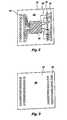
- FIG. 1is a cross-sectional view of a stack of a first embodiment of the packaged semiconductor dice of the present invention on a printed circuit board;
- FIG. 2is a top view of a packaged semiconductor die of the present invention
- FIG. 3is a bottom view of a packaged semiconductor die of the present invention.
- FIG. 4is a cross-sectional view of stacks of the packaged semiconductor dice of the present invention on both sides of a printed circuit board;
- FIG. 5is a cross-sectional view of a stack of a second embodiment of the packaged semiconductor die of the present invention on a printed circuit board;
- FIG. 6is a cross-sectional view of stacks of the second embodiment of the present invention on both sides of a printed circuit board.
- each carrier 12comprises a member having a cavity 16 therein.
- the cavity 16may be a single-level or multi-level cavity having any desired number of levels therein.
- the carrier 12is formed having a plurality of contact pads 18 located on the upper surface 20 and lower surface 22 thereof which is connected by circuits 24 (not shown) and by wire bonds 26 to the bond pads 28 located on the active surface 30 of the semiconductor die or device 14 .
- the semiconductor die or device 14is initially retained within the cavity 16 by any suitable means, such as adhesive, etc.
- the circuits 24are formed on the upper surface 20 of the carrier 12 and portions of the walls or surfaces of the cavity 16 by any suitable well-known means, such as deposition and etching processes.
- the wire bonds connecting the bond pads 28 of the semiconductor die or device 14 to the circuits 24 (not shown)are made using any suitable commercially available wire bonder.
- the cavity 16is filled with suitable encapsulant material 32 covering and sealing the semiconductor die 14 in the cavity 16 and sealing the wire bonds 26 in position therein.
- the carriers 12may be of any desired geometric shape.
- the carrier 12is formed having internal circuits 34 extending between the contact pads 18 on the upper surface 20 and lower surface 22 of the carrier 12 .
- the carrier 12is formed having frustoconical recess surfaces 36 , lips 38 , and frustoconical surfaces 40 on the upper surface 20 .
- the surfaces 36 and 40are formed having complementary angles so that the surfaces 36 and lips 38 of an adjacent carrier 12 mate or nest with an adjacent carrier 12 having surfaces 40 thereon, thereby forming a stable, self-aligning stack of carriers 12 .
- the carriers 12may be formed having a plurality of heat transfer fins 42 thereon.
- the carrier 12may be formed of any desired suitable material, such as ceramic material, high-temperature plastic material, etc.
- the carrier 12may be formed by any suitable method, such as molding, extrusion, etc.
- the assemblyis connected to the substrate 2 using a plurality of reflowed solder balls 50 .
- the substrate 2includes circuitry thereon, on either the upper surface or lower surface or both, and therein, as well as conductive vias, if desired.
- the substrate 2may be any suitable substrate, such as a printed circuit board, FR-4 board, etc. Any desired number of carriers 12 may be stacked to form an assembly on the substrate 2 .
- the reflowed solder balls 50are located in alignment with the contact pads 18 and the connecting internal circuits 34 extending between the contact pads 18 on the upper surface 20 and lower surface 22 of a carrier 12 .
- a carrier 12 having circuits 24 thereon extending between contact pads 18 on the upper surface 20 of the carrier 12is illustrated.
- circuits 24extending on the surface 20 of the carrier 12 is illustrated.
- the bottom surface 22 of a carrier 12is illustrated having a plurality of contact pads 18 located thereon.
- a plurality of assemblies 10is illustrated located on both sides of a substrate 2 being connected to the circuitry thereon by a plurality of reflowed solder balls 50 .
- a second embodiment of the present inventionis illustrated.
- a plurality of assemblies 100is stacked on a substrate 2 , being electrically and mechanically connected thereto by reflowed solder balls 150 .
- Each assembly 100comprises a carrier 112 having a cavity 116 therein containing a semiconductor die or device 114 therein.
- the semiconductor die or device 114is electrically connected to the circuits 134 of the carrier 112 by reflowed solder balls 126 .
- Each carrier 112is formed having apertures 160 therethrough connecting with circuits 134 .
- Each carrier 112is formed with surfaces 136 and 140 as well as lips 138 as described hereinbefore with respect to carrier 12 .
- a conductive material 162such as conductive epoxy, solder, etc., is used to fill the apertures 160 in the carriers and contact the conductive material 162 in adjacent carriers 112 .
- the carriers 112are similar in construction to the carriers 12 as described hereinbefore, except for the apertures 160 , conductive material 162 , circuits 134 , and reflowed solder balls 126 between the semiconductor die or device 114 and the circuits 134 .
- the substrate 2is the same as described hereinbefore.
- a plurality of assemblies 100is illustrated stacked on both sides of a substrate 2 , being electrically and mechanically connected thereto by reflowed solder balls 150 .
Landscapes
- Engineering & Computer Science (AREA)
- Power Engineering (AREA)
- Microelectronics & Electronic Packaging (AREA)
- Physics & Mathematics (AREA)
- Condensed Matter Physics & Semiconductors (AREA)
- General Physics & Mathematics (AREA)
- Computer Hardware Design (AREA)
- Structures Or Materials For Encapsulating Or Coating Semiconductor Devices Or Solid State Devices (AREA)
- Cooling Or The Like Of Semiconductors Or Solid State Devices (AREA)
- Semiconductor Integrated Circuits (AREA)
Abstract
Description
- This application is a continuation of application Ser. No. 10/706,210, filed Nov. 12, 2003, pending, which is a divisional of application Ser. No. 09/924,635, filed Aug. 8, 2001, now U.S. Pat. No. 6,650,007, issued Nov. 18, 2003, which is a continuation of application Ser. No. 09/344,279, filed Jun. 30, 1999, now U.S. Pat. No. 6,297,548, issued Oct. 2, 2001, which claims the benefit of U.S. Provisional Application No. 60/091,205 filed Jun. 30, 1998.
- 1. Statement of the Invention
- The present invention relates to an apparatus for high-temperature thermal applications for ball grid array semiconductor devices and a method of packaging ball grid array semiconductor devices.
- 2. State of the Art
- Integrated semiconductor devices are typically constructed in wafer form with each device having the form of an integrated circuit die which is typically attached to a lead frame with gold wires. The die and lead frame are then encapsulated in a plastic or ceramic package, which is then commonly referred to as an integrated circuit (IC). ICs come in a variety of forms, such as a dynamic random access memory (DRAM), static random access memory (SRAM), read only memory (ROM), gate arrays, etc. The ICs are interconnected in many combinations on printed circuit boards by a number of techniques, such as socketing and soldering. Interconnection among ICs arrayed on a printed circuit board is typically made by conductive traces formed by photolithography and etching processes.
- Such semiconductor devices typically take the form of the semiconductor die therein. The die is generally electrically attached to a lead frame within a package. The lead frame physically supports the die and provides electrical connections between the die and its operating environment. The die is generally electrically attached to the lead frame by means of fine gold wires. These fine gold wires function to connect the die to the lead frame so that the gold wires are connected electrically in series with the lead frame leads. The lead frame and die are then encapsulated. The packaged chip is then able to be installed on a circuit board by any desired manner, such as soldering, socketing, etc.
- However, as the speed of the semiconductor die increases, the heat generated during operation increases. Additionally, it becomes necessary to shorten the leads between the printed circuit board on which the IC is located and the IC device itself in order to keep the impedance of the circuit from affecting the response speed of the IC device.
- The wires connecting the leads of the lead frame to the bond pads on the active surface of the semiconductor die in an IC package are not an effective connection for high operating speed semiconductor dice as the wires slow down the response of the semiconductor die.
- Therefore, a packaging is required for semiconductor dice which have high operating speeds and generate heat associated therewith while minimizing the lead length between the semiconductor dice and the printed circuit boards on which they are mounted.
- The present invention comprises an apparatus package for high-temperature thermal applications for ball grid array semiconductor devices and a method of packaging ball grid array semiconductor devices.
FIG. 1 is a cross-sectional view of a stack of a first embodiment of the packaged semiconductor dice of the present invention on a printed circuit board;FIG. 2 is a top view of a packaged semiconductor die of the present invention;FIG. 3 is a bottom view of a packaged semiconductor die of the present invention;FIG. 4 is a cross-sectional view of stacks of the packaged semiconductor dice of the present invention on both sides of a printed circuit board;FIG. 5 is a cross-sectional view of a stack of a second embodiment of the packaged semiconductor die of the present invention on a printed circuit board; andFIG. 6 is a cross-sectional view of stacks of the second embodiment of the present invention on both sides of a printed circuit board.- The present invention will be better understood when the drawings are taken in conjunction with the description of the invention.
- Referring to drawing
FIG. 1 , a plurality ofassemblies 10 comprising acarrier 12 and asemiconductor device 14 located therein is illustrated installed on asubstrate 2. Eachcarrier 12 comprises a member having acavity 16 therein. As illustrated, thecavity 16 may be a single-level or multi-level cavity having any desired number of levels therein. Thecarrier 12 is formed having a plurality ofcontact pads 18 located on theupper surface 20 andlower surface 22 thereof which is connected by circuits24 (not shown) and bywire bonds 26 to thebond pads 28 located on theactive surface 30 of the semiconductor die ordevice 14. The semiconductor die ordevice 14 is initially retained within thecavity 16 by any suitable means, such as adhesive, etc. The circuits24 (not shown) are formed on theupper surface 20 of thecarrier 12 and portions of the walls or surfaces of thecavity 16 by any suitable well-known means, such as deposition and etching processes. The wire bonds connecting thebond pads 28 of the semiconductor die ordevice 14 to the circuits24 (not shown) are made using any suitable commercially available wire bonder. After thewire bonds 26 are formed, thecavity 16 is filled with suitableencapsulant material 32 covering and sealing the semiconductor die14 in thecavity 16 and sealing thewire bonds 26 in position therein. - The
carriers 12 may be of any desired geometric shape. Thecarrier 12 is formed havinginternal circuits 34 extending between thecontact pads 18 on theupper surface 20 andlower surface 22 of thecarrier 12. Thecarrier 12 is formed havingfrustoconical recess surfaces 36,lips 38, andfrustoconical surfaces 40 on theupper surface 20. Thesurfaces surfaces 36 andlips 38 of anadjacent carrier 12 mate or nest with anadjacent carrier 12 havingsurfaces 40 thereon, thereby forming a stable, self-aligning stack ofcarriers 12. If desired, thecarriers 12 may be formed having a plurality ofheat transfer fins 42 thereon. Thecarrier 12 may be formed of any desired suitable material, such as ceramic material, high-temperature plastic material, etc. Thecarrier 12 may be formed by any suitable method, such as molding, extrusion, etc. - Once a plurality of
carriers 12 having semiconductor die ordevices 14 therein is formed as an assembly, the assembly is connected to thesubstrate 2 using a plurality of reflowedsolder balls 50. Thesubstrate 2 includes circuitry thereon, on either the upper surface or lower surface or both, and therein, as well as conductive vias, if desired. Thesubstrate 2 may be any suitable substrate, such as a printed circuit board, FR-4 board, etc. Any desired number ofcarriers 12 may be stacked to form an assembly on thesubstrate 2. As illustrated, the reflowedsolder balls 50 are located in alignment with thecontact pads 18 and the connectinginternal circuits 34 extending between thecontact pads 18 on theupper surface 20 andlower surface 22 of acarrier 12. - Referring to drawing
FIG. 2 , acarrier 12 havingcircuits 24 thereon extending betweencontact pads 18 on theupper surface 20 of thecarrier 12 is illustrated. For purposes of clarity, only a portion of thecircuits 24 extending on thesurface 20 of thecarrier 12 is illustrated. - Referring to drawing
FIG. 3 , thebottom surface 22 of acarrier 12 is illustrated having a plurality ofcontact pads 18 located thereon. - Referring to drawing
FIG. 4 , a plurality ofassemblies 10 is illustrated located on both sides of asubstrate 2 being connected to the circuitry thereon by a plurality of reflowedsolder balls 50. - Referring to drawing
FIG. 5 , a second embodiment of the present invention is illustrated. A plurality ofassemblies 100 is stacked on asubstrate 2, being electrically and mechanically connected thereto by reflowedsolder balls 150. Eachassembly 100 comprises acarrier 112 having acavity 116 therein containing a semiconductor die ordevice 114 therein. The semiconductor die ordevice 114 is electrically connected to thecircuits 134 of thecarrier 112 by reflowedsolder balls 126. Eachcarrier 112 is formed havingapertures 160 therethrough connecting withcircuits 134. Eachcarrier 112 is formed withsurfaces lips 138 as described hereinbefore with respect tocarrier 12. To connect eachcarrier 112 to anadjacent carrier 112, aconductive material 162, such as conductive epoxy, solder, etc., is used to fill theapertures 160 in the carriers and contact theconductive material 162 inadjacent carriers 112. - The
carriers 112 are similar in construction to thecarriers 12 as described hereinbefore, except for theapertures 160,conductive material 162,circuits 134, and reflowedsolder balls 126 between the semiconductor die ordevice 114 and thecircuits 134. - The
substrate 2 is the same as described hereinbefore. - Referring to drawing
FIG. 6 , a plurality ofassemblies 100 is illustrated stacked on both sides of asubstrate 2, being electrically and mechanically connected thereto by reflowedsolder balls 150. - The present invention includes additions, deletions, modifications, and alterations which are within the scope of the claims.
Claims (45)
Priority Applications (2)
| Application Number | Priority Date | Filing Date | Title |
|---|---|---|---|
| US11/063,403US7285442B2 (en) | 1998-06-30 | 2005-02-22 | Stackable ceramic FBGA for high thermal applications |
| US11/874,531US7829991B2 (en) | 1998-06-30 | 2007-10-18 | Stackable ceramic FBGA for high thermal applications |
Applications Claiming Priority (5)
| Application Number | Priority Date | Filing Date | Title |
|---|---|---|---|
| US9120598P | 1998-06-30 | 1998-06-30 | |
| US09/344,279US6297548B1 (en) | 1998-06-30 | 1999-06-30 | Stackable ceramic FBGA for high thermal applications |
| US09/924,635US6650007B2 (en) | 1998-06-30 | 2001-08-08 | Stackable ceramic fbga for high thermal applications |
| US10/706,210US6858926B2 (en) | 1998-06-30 | 2003-11-12 | Stackable ceramic FBGA for high thermal applications |
| US11/063,403US7285442B2 (en) | 1998-06-30 | 2005-02-22 | Stackable ceramic FBGA for high thermal applications |
Related Parent Applications (1)
| Application Number | Title | Priority Date | Filing Date |
|---|---|---|---|
| US10/706,210ContinuationUS6858926B2 (en) | 1998-06-30 | 2003-11-12 | Stackable ceramic FBGA for high thermal applications |
Related Child Applications (1)
| Application Number | Title | Priority Date | Filing Date |
|---|---|---|---|
| US11/874,531DivisionUS7829991B2 (en) | 1998-06-30 | 2007-10-18 | Stackable ceramic FBGA for high thermal applications |
Publications (2)
| Publication Number | Publication Date |
|---|---|
| US20050146010A1true US20050146010A1 (en) | 2005-07-07 |
| US7285442B2 US7285442B2 (en) | 2007-10-23 |
Family
ID=26783710
Family Applications (5)
| Application Number | Title | Priority Date | Filing Date |
|---|---|---|---|
| US09/344,279Expired - LifetimeUS6297548B1 (en) | 1998-06-30 | 1999-06-30 | Stackable ceramic FBGA for high thermal applications |
| US09/924,635Expired - LifetimeUS6650007B2 (en) | 1998-06-30 | 2001-08-08 | Stackable ceramic fbga for high thermal applications |
| US10/706,210Expired - Fee RelatedUS6858926B2 (en) | 1998-06-30 | 2003-11-12 | Stackable ceramic FBGA for high thermal applications |
| US11/063,403Expired - LifetimeUS7285442B2 (en) | 1998-06-30 | 2005-02-22 | Stackable ceramic FBGA for high thermal applications |
| US11/874,531Expired - Fee RelatedUS7829991B2 (en) | 1998-06-30 | 2007-10-18 | Stackable ceramic FBGA for high thermal applications |
Family Applications Before (3)
| Application Number | Title | Priority Date | Filing Date |
|---|---|---|---|
| US09/344,279Expired - LifetimeUS6297548B1 (en) | 1998-06-30 | 1999-06-30 | Stackable ceramic FBGA for high thermal applications |
| US09/924,635Expired - LifetimeUS6650007B2 (en) | 1998-06-30 | 2001-08-08 | Stackable ceramic fbga for high thermal applications |
| US10/706,210Expired - Fee RelatedUS6858926B2 (en) | 1998-06-30 | 2003-11-12 | Stackable ceramic FBGA for high thermal applications |
Family Applications After (1)
| Application Number | Title | Priority Date | Filing Date |
|---|---|---|---|
| US11/874,531Expired - Fee RelatedUS7829991B2 (en) | 1998-06-30 | 2007-10-18 | Stackable ceramic FBGA for high thermal applications |
Country Status (1)
| Country | Link |
|---|---|
| US (5) | US6297548B1 (en) |
Cited By (3)
| Publication number | Priority date | Publication date | Assignee | Title |
|---|---|---|---|---|
| US20040124520A1 (en)* | 2002-10-22 | 2004-07-01 | Rinne Glenn A. | Stacked electronic structures including offset substrates |
| US20090140408A1 (en)* | 2007-11-30 | 2009-06-04 | Taewoo Lee | Integrated circuit package-on-package system with stacking via interconnect |
| US8674494B2 (en) | 2011-08-31 | 2014-03-18 | Samsung Electronics Co., Ltd. | Semiconductor package having supporting plate and method of forming the same |
Families Citing this family (177)
| Publication number | Priority date | Publication date | Assignee | Title |
|---|---|---|---|---|
| US6893900B1 (en) | 1998-06-24 | 2005-05-17 | Amkor Technology, Inc. | Method of making an integrated circuit package |
| US7005326B1 (en) | 1998-06-24 | 2006-02-28 | Amkor Technology, Inc. | Method of making an integrated circuit package |
| US7030474B1 (en) | 1998-06-24 | 2006-04-18 | Amkor Technology, Inc. | Plastic integrated circuit package and method and leadframe for making the package |
| US6143981A (en) | 1998-06-24 | 2000-11-07 | Amkor Technology, Inc. | Plastic integrated circuit package and method and leadframe for making the package |
| US7071541B1 (en) | 1998-06-24 | 2006-07-04 | Amkor Technology, Inc. | Plastic integrated circuit package and method and leadframe for making the package |
| US7112474B1 (en) | 1998-06-24 | 2006-09-26 | Amkor Technology, Inc. | Method of making an integrated circuit package |
| US7332375B1 (en) | 1998-06-24 | 2008-02-19 | Amkor Technology, Inc. | Method of making an integrated circuit package |
| US6297548B1 (en)* | 1998-06-30 | 2001-10-02 | Micron Technology, Inc. | Stackable ceramic FBGA for high thermal applications |
| US6153929A (en) | 1998-08-21 | 2000-11-28 | Micron Technology, Inc. | Low profile multi-IC package connector |
| US6448633B1 (en) | 1998-11-20 | 2002-09-10 | Amkor Technology, Inc. | Semiconductor package and method of making using leadframe having lead locks to secure leads to encapsulant |
| JP3685947B2 (en)* | 1999-03-15 | 2005-08-24 | 新光電気工業株式会社 | Semiconductor device and manufacturing method thereof |
| KR20010037247A (en) | 1999-10-15 | 2001-05-07 | 마이클 디. 오브라이언 | Semiconductor package |
| KR100403142B1 (en) | 1999-10-15 | 2003-10-30 | 앰코 테크놀로지 코리아 주식회사 | semiconductor package |
| KR100379089B1 (en) | 1999-10-15 | 2003-04-08 | 앰코 테크놀로지 코리아 주식회사 | leadframe and semiconductor package using it |
| US6580159B1 (en) | 1999-11-05 | 2003-06-17 | Amkor Technology, Inc. | Integrated circuit device packages and substrates for making the packages |
| US6847103B1 (en) | 1999-11-09 | 2005-01-25 | Amkor Technology, Inc. | Semiconductor package with exposed die pad and body-locking leadframe |
| KR100421774B1 (en) | 1999-12-16 | 2004-03-10 | 앰코 테크놀로지 코리아 주식회사 | semiconductor package and its manufacturing method |
| KR100426494B1 (en)* | 1999-12-20 | 2004-04-13 | 앰코 테크놀로지 코리아 주식회사 | Semiconductor package and its manufacturing method |
| KR20010068781A (en)* | 2000-01-10 | 2001-07-23 | 윤종용 | Semiconductor chip package |
| KR100583494B1 (en) | 2000-03-25 | 2006-05-24 | 앰코 테크놀로지 코리아 주식회사 | Semiconductor Package |
| US7042068B2 (en) | 2000-04-27 | 2006-05-09 | Amkor Technology, Inc. | Leadframe and semiconductor package made using the leadframe |
| KR20020058209A (en) | 2000-12-29 | 2002-07-12 | 마이클 디. 오브라이언 | Semiconductor package |
| US20030221313A1 (en)* | 2001-01-26 | 2003-12-04 | Gann Keith D. | Method for making stacked integrated circuits (ICs) using prepackaged parts |
| JP2002305286A (en)* | 2001-02-01 | 2002-10-18 | Mitsubishi Electric Corp | Semiconductor modules and electronic components |
| US6967395B1 (en) | 2001-03-20 | 2005-11-22 | Amkor Technology, Inc. | Mounting for a package containing a chip |
| US6545345B1 (en) | 2001-03-20 | 2003-04-08 | Amkor Technology, Inc. | Mounting for a package containing a chip |
| KR100369393B1 (en) | 2001-03-27 | 2003-02-05 | 앰코 테크놀로지 코리아 주식회사 | Lead frame and semiconductor package using it and its manufacturing method |
| KR100393448B1 (en) | 2001-03-27 | 2003-08-02 | 앰코 테크놀로지 코리아 주식회사 | Semiconductor package and method for manufacturing the same |
| US7045883B1 (en) | 2001-04-04 | 2006-05-16 | Amkor Technology, Inc. | Thermally enhanced chip scale lead on chip semiconductor package and method of making same |
| US6597059B1 (en) | 2001-04-04 | 2003-07-22 | Amkor Technology, Inc. | Thermally enhanced chip scale lead on chip semiconductor package |
| US7064009B1 (en) | 2001-04-04 | 2006-06-20 | Amkor Technology, Inc. | Thermally enhanced chip scale lead on chip semiconductor package and method of making same |
| US6586826B1 (en)* | 2001-06-13 | 2003-07-01 | Amkor Technology, Inc. | Integrated circuit package having posts for connection to other packages and substrates |
| US6900527B1 (en) | 2001-09-19 | 2005-05-31 | Amkor Technology, Inc. | Lead-frame method and assembly for interconnecting circuits within a circuit module |
| US7485952B1 (en) | 2001-09-19 | 2009-02-03 | Amkor Technology, Inc. | Drop resistant bumpers for fully molded memory cards |
| US20040173894A1 (en)* | 2001-09-27 | 2004-09-09 | Amkor Technology, Inc. | Integrated circuit package including interconnection posts for multiple electrical connections |
| US6630726B1 (en) | 2001-11-07 | 2003-10-07 | Amkor Technology, Inc. | Power semiconductor package with strap |
| US7332819B2 (en)* | 2002-01-09 | 2008-02-19 | Micron Technology, Inc. | Stacked die in die BGA package |
| SG152909A1 (en)* | 2002-01-09 | 2009-06-29 | Micron Technology Inc | Stacked die in die bga package |
| SG115456A1 (en) | 2002-03-04 | 2005-10-28 | Micron Technology Inc | Semiconductor die packages with recessed interconnecting structures and methods for assembling the same |
| SG121707A1 (en)* | 2002-03-04 | 2006-05-26 | Micron Technology Inc | Method and apparatus for flip-chip packaging providing testing capability |
| US6608366B1 (en) | 2002-04-15 | 2003-08-19 | Harry J. Fogelson | Lead frame with plated end leads |
| US7132311B2 (en)* | 2002-07-26 | 2006-11-07 | Intel Corporation | Encapsulation of a stack of semiconductor dice |
| US7087988B2 (en)* | 2002-07-30 | 2006-08-08 | Kabushiki Kaisha Toshiba | Semiconductor packaging apparatus |
| US6927497B2 (en)* | 2002-08-22 | 2005-08-09 | Intel Corporation | Multi-die semiconductor package |
| US6818973B1 (en) | 2002-09-09 | 2004-11-16 | Amkor Technology, Inc. | Exposed lead QFP package fabricated through the use of a partial saw process |
| US6919620B1 (en) | 2002-09-17 | 2005-07-19 | Amkor Technology, Inc. | Compact flash memory card with clamshell leadframe |
| US6998328B2 (en)* | 2002-11-06 | 2006-02-14 | Irvine Sensors Corp. | Method for creating neo-wafers from singulated integrated circuit die and a device made according to the method |
| US7361533B1 (en) | 2002-11-08 | 2008-04-22 | Amkor Technology, Inc. | Stacked embedded leadframe |
| US6905914B1 (en) | 2002-11-08 | 2005-06-14 | Amkor Technology, Inc. | Wafer level package and fabrication method |
| US7723210B2 (en) | 2002-11-08 | 2010-05-25 | Amkor Technology, Inc. | Direct-write wafer level chip scale package |
| US7190062B1 (en) | 2004-06-15 | 2007-03-13 | Amkor Technology, Inc. | Embedded leadframe semiconductor package |
| US6798047B1 (en) | 2002-12-26 | 2004-09-28 | Amkor Technology, Inc. | Pre-molded leadframe |
| US6847099B1 (en) | 2003-02-05 | 2005-01-25 | Amkor Technology Inc. | Offset etched corner leads for semiconductor package |
| US6750545B1 (en) | 2003-02-28 | 2004-06-15 | Amkor Technology, Inc. | Semiconductor package capable of die stacking |
| US6794740B1 (en) | 2003-03-13 | 2004-09-21 | Amkor Technology, Inc. | Leadframe package for semiconductor devices |
| US7001799B1 (en) | 2003-03-13 | 2006-02-21 | Amkor Technology, Inc. | Method of making a leadframe for semiconductor devices |
| JP3846437B2 (en)* | 2003-03-17 | 2006-11-15 | 株式会社日立製作所 | Automotive control unit |
| US6879034B1 (en) | 2003-05-01 | 2005-04-12 | Amkor Technology, Inc. | Semiconductor package including low temperature co-fired ceramic substrate |
| US7095103B1 (en) | 2003-05-01 | 2006-08-22 | Amkor Technology, Inc. | Leadframe based memory card |
| TWI231023B (en)* | 2003-05-27 | 2005-04-11 | Ind Tech Res Inst | Electronic packaging with three-dimensional stack and assembling method thereof |
| US7008825B1 (en) | 2003-05-27 | 2006-03-07 | Amkor Technology, Inc. | Leadframe strip having enhanced testability |
| US6897550B1 (en) | 2003-06-11 | 2005-05-24 | Amkor Technology, Inc. | Fully-molded leadframe stand-off feature |
| KR100604821B1 (en) | 2003-06-30 | 2006-07-26 | 삼성전자주식회사 | Stacked ball grid array package and its manufacturing method |
| US20050018408A1 (en)* | 2003-07-24 | 2005-01-27 | Rivkin David Aaron | Multiple mounting, self aligning, electronics enclosure (multimount) |
| US7245007B1 (en) | 2003-09-18 | 2007-07-17 | Amkor Technology, Inc. | Exposed lead interposer leadframe package |
| US6921967B2 (en) | 2003-09-24 | 2005-07-26 | Amkor Technology, Inc. | Reinforced die pad support structure |
| DE10348620A1 (en)* | 2003-10-15 | 2005-06-02 | Infineon Technologies Ag | Semiconductor module with housing contacts |
| US7138707B1 (en) | 2003-10-21 | 2006-11-21 | Amkor Technology, Inc. | Semiconductor package including leads and conductive posts for providing increased functionality |
| US7144517B1 (en) | 2003-11-07 | 2006-12-05 | Amkor Technology, Inc. | Manufacturing method for leadframe and for semiconductor package using the leadframe |
| US7211879B1 (en) | 2003-11-12 | 2007-05-01 | Amkor Technology, Inc. | Semiconductor package with chamfered corners and method of manufacturing the same |
| US7057268B1 (en) | 2004-01-27 | 2006-06-06 | Amkor Technology, Inc. | Cavity case with clip/plug for use on multi-media card |
| US7091594B1 (en) | 2004-01-28 | 2006-08-15 | Amkor Technology, Inc. | Leadframe type semiconductor package having reduced inductance and its manufacturing method |
| US7145249B2 (en)* | 2004-03-29 | 2006-12-05 | Intel Corporation | Semiconducting device with folded interposer |
| US7378725B2 (en)* | 2004-03-31 | 2008-05-27 | Intel Corporation | Semiconducting device with stacked dice |
| US7067910B2 (en)* | 2004-04-13 | 2006-06-27 | Sun Microsystems, Inc. | Method and apparatus for using capacitively coupled communication within stacks of laminated chips |
| GB2429582B (en) | 2004-05-11 | 2009-02-11 | Spansion Llc | Carrier for stacked type semiconductor device and method of fabricating the same |
| US7190815B2 (en)* | 2004-05-26 | 2007-03-13 | Topaz Systems, Inc. | Method for authenticating an electronic signature |
| US20050275081A1 (en)* | 2004-06-12 | 2005-12-15 | Roger Chang | Embedded chip semiconductor having dual electronic connection faces |
| US20050285254A1 (en)* | 2004-06-23 | 2005-12-29 | Buot Joan R V | Semiconducting device having stacked dice |
| US7202554B1 (en) | 2004-08-19 | 2007-04-10 | Amkor Technology, Inc. | Semiconductor package and its manufacturing method |
| US7602618B2 (en)* | 2004-08-25 | 2009-10-13 | Micron Technology, Inc. | Methods and apparatuses for transferring heat from stacked microfeature devices |
| US7217991B1 (en) | 2004-10-22 | 2007-05-15 | Amkor Technology, Inc. | Fan-in leadframe semiconductor package |
| DE102005003390B4 (en)* | 2005-01-24 | 2007-09-13 | Qimonda Ag | Substrate for an FBGA semiconductor device |
| US20070109756A1 (en)* | 2005-02-10 | 2007-05-17 | Stats Chippac Ltd. | Stacked integrated circuits package system |
| US20080203552A1 (en)* | 2005-02-15 | 2008-08-28 | Unisemicon Co., Ltd. | Stacked Package and Method of Fabricating the Same |
| US7250675B2 (en)* | 2005-05-05 | 2007-07-31 | International Business Machines Corporation | Method and apparatus for forming stacked die and substrate structures for increased packing density |
| KR20070009136A (en)* | 2005-07-15 | 2007-01-18 | 삼성전자주식회사 | A packaging chip comprising a through electrode directly connected to a plurality of wafers and a manufacturing method thereof |
| KR100631959B1 (en)* | 2005-09-07 | 2006-10-04 | 주식회사 하이닉스반도체 | Multilayer semiconductor package and manufacturing method thereof |
| JP4473807B2 (en)* | 2005-10-27 | 2010-06-02 | パナソニック株式会社 | Multilayer semiconductor device and lower layer module of multilayer semiconductor device |
| US7507603B1 (en) | 2005-12-02 | 2009-03-24 | Amkor Technology, Inc. | Etch singulated semiconductor package |
| US7572681B1 (en) | 2005-12-08 | 2009-08-11 | Amkor Technology, Inc. | Embedded electronic component package |
| US7902660B1 (en) | 2006-05-24 | 2011-03-08 | Amkor Technology, Inc. | Substrate for semiconductor device and manufacturing method thereof |
| US7615863B2 (en)* | 2006-06-19 | 2009-11-10 | Northrop Grumman Space & Missions Systems Corp. | Multi-dimensional wafer-level integrated antenna sensor micro packaging |
| US7968998B1 (en) | 2006-06-21 | 2011-06-28 | Amkor Technology, Inc. | Side leaded, bottom exposed pad and bottom exposed lead fusion quad flat semiconductor package |
| US7888185B2 (en)* | 2006-08-17 | 2011-02-15 | Micron Technology, Inc. | Semiconductor device assemblies and systems including at least one conductive pathway extending around a side of at least one semiconductor device |
| US7687893B2 (en) | 2006-12-27 | 2010-03-30 | Amkor Technology, Inc. | Semiconductor package having leadframe with exposed anchor pads |
| US7829990B1 (en) | 2007-01-18 | 2010-11-09 | Amkor Technology, Inc. | Stackable semiconductor package including laminate interposer |
| US20080179721A1 (en)* | 2007-01-31 | 2008-07-31 | Cheng-Lien Chiang | Stacking of transfer carriers with aperture arrays as interconnection joints |
| US20090206481A1 (en)* | 2007-01-31 | 2009-08-20 | Nichepac Technology Inc. | Stacking of transfer carriers with aperture arrays as interconnection joints |
| US7982297B1 (en) | 2007-03-06 | 2011-07-19 | Amkor Technology, Inc. | Stackable semiconductor package having partially exposed semiconductor die and method of fabricating the same |
| US7977774B2 (en) | 2007-07-10 | 2011-07-12 | Amkor Technology, Inc. | Fusion quad flat semiconductor package |
| US7687899B1 (en) | 2007-08-07 | 2010-03-30 | Amkor Technology, Inc. | Dual laminate package structure with embedded elements |
| US7777351B1 (en) | 2007-10-01 | 2010-08-17 | Amkor Technology, Inc. | Thin stacked interposer package |
| KR101413220B1 (en)* | 2007-10-02 | 2014-06-30 | 삼성전자주식회사 | Semiconductor package having interposer and method for manufacturing semiconductor package |
| US8089159B1 (en) | 2007-10-03 | 2012-01-03 | Amkor Technology, Inc. | Semiconductor package with increased I/O density and method of making the same |
| US7847386B1 (en) | 2007-11-05 | 2010-12-07 | Amkor Technology, Inc. | Reduced size stacked semiconductor package and method of making the same |
| US7956453B1 (en) | 2008-01-16 | 2011-06-07 | Amkor Technology, Inc. | Semiconductor package with patterning layer and method of making same |
| US7723852B1 (en) | 2008-01-21 | 2010-05-25 | Amkor Technology, Inc. | Stacked semiconductor package and method of making same |
| US7863755B2 (en)* | 2008-03-19 | 2011-01-04 | Stats Chippac Ltd. | Package-on-package system with via Z-interconnections |
| US8067821B1 (en) | 2008-04-10 | 2011-11-29 | Amkor Technology, Inc. | Flat semiconductor package with half package molding |
| US7768135B1 (en) | 2008-04-17 | 2010-08-03 | Amkor Technology, Inc. | Semiconductor package with fast power-up cycle and method of making same |
| SG142321A1 (en) | 2008-04-24 | 2009-11-26 | Micron Technology Inc | Pre-encapsulated cavity interposer |
| US7808084B1 (en) | 2008-05-06 | 2010-10-05 | Amkor Technology, Inc. | Semiconductor package with half-etched locking features |
| US7745920B2 (en)* | 2008-06-10 | 2010-06-29 | Micron Technology, Inc. | Packaged microelectronic devices and methods for manufacturing packaged microelectronic devices |
| US8125064B1 (en) | 2008-07-28 | 2012-02-28 | Amkor Technology, Inc. | Increased I/O semiconductor package and method of making same |
| US8184453B1 (en) | 2008-07-31 | 2012-05-22 | Amkor Technology, Inc. | Increased capacity semiconductor package |
| KR20100033012A (en)* | 2008-09-19 | 2010-03-29 | 주식회사 하이닉스반도체 | Semiconductor package and stacked semiconductor package having the same |
| US7847392B1 (en) | 2008-09-30 | 2010-12-07 | Amkor Technology, Inc. | Semiconductor device including leadframe with increased I/O |
| US7989933B1 (en) | 2008-10-06 | 2011-08-02 | Amkor Technology, Inc. | Increased I/O leadframe and semiconductor device including same |
| US8008758B1 (en) | 2008-10-27 | 2011-08-30 | Amkor Technology, Inc. | Semiconductor device with increased I/O leadframe |
| TWI437674B (en)* | 2008-11-17 | 2014-05-11 | Advanpack Solutions Pte Ltd | Semiconductor substrate, package and device |
| US8089145B1 (en) | 2008-11-17 | 2012-01-03 | Amkor Technology, Inc. | Semiconductor device including increased capacity leadframe |
| US8072050B1 (en) | 2008-11-18 | 2011-12-06 | Amkor Technology, Inc. | Semiconductor device with increased I/O leadframe including passive device |
| US7875963B1 (en) | 2008-11-21 | 2011-01-25 | Amkor Technology, Inc. | Semiconductor device including leadframe having power bars and increased I/O |
| US7982298B1 (en) | 2008-12-03 | 2011-07-19 | Amkor Technology, Inc. | Package in package semiconductor device |
| US8487420B1 (en) | 2008-12-08 | 2013-07-16 | Amkor Technology, Inc. | Package in package semiconductor device with film over wire |
| US8680656B1 (en) | 2009-01-05 | 2014-03-25 | Amkor Technology, Inc. | Leadframe structure for concentrated photovoltaic receiver package |
| US20170117214A1 (en) | 2009-01-05 | 2017-04-27 | Amkor Technology, Inc. | Semiconductor device with through-mold via |
| US8058715B1 (en) | 2009-01-09 | 2011-11-15 | Amkor Technology, Inc. | Package in package device for RF transceiver module |
| US8026589B1 (en) | 2009-02-23 | 2011-09-27 | Amkor Technology, Inc. | Reduced profile stackable semiconductor package |
| US7960818B1 (en) | 2009-03-04 | 2011-06-14 | Amkor Technology, Inc. | Conformal shield on punch QFN semiconductor package |
| US8367477B2 (en)* | 2009-03-13 | 2013-02-05 | Wen-Cheng Chien | Electronic device package and method for forming the same |
| US8575742B1 (en) | 2009-04-06 | 2013-11-05 | Amkor Technology, Inc. | Semiconductor device with increased I/O leadframe including power bars |
| US8119447B2 (en)* | 2009-06-17 | 2012-02-21 | Stats Chippac Ltd. | Integrated circuit packaging system with through via die having pedestal and recess and method of manufacture thereof |
| US8310835B2 (en) | 2009-07-14 | 2012-11-13 | Apple Inc. | Systems and methods for providing vias through a modular component |
| US8796561B1 (en) | 2009-10-05 | 2014-08-05 | Amkor Technology, Inc. | Fan out build up substrate stackable package and method |
| DE102009048838B3 (en)* | 2009-10-09 | 2011-01-20 | Eads Deutschland Gmbh | Hermetic dense high-frequency frontend |
| US8937381B1 (en) | 2009-12-03 | 2015-01-20 | Amkor Technology, Inc. | Thin stackable package and method |
| US9691734B1 (en) | 2009-12-07 | 2017-06-27 | Amkor Technology, Inc. | Method of forming a plurality of electronic component packages |
| US9219023B2 (en)* | 2010-01-19 | 2015-12-22 | Globalfoundries Inc. | 3D chip stack having encapsulated chip-in-chip |
| US8324511B1 (en) | 2010-04-06 | 2012-12-04 | Amkor Technology, Inc. | Through via nub reveal method and structure |
| US8294276B1 (en) | 2010-05-27 | 2012-10-23 | Amkor Technology, Inc. | Semiconductor device and fabricating method thereof |
| JP2012008695A (en)* | 2010-06-23 | 2012-01-12 | Elpida Memory Inc | Memory system, memory module, and module socket |
| US8847376B2 (en) | 2010-07-23 | 2014-09-30 | Tessera, Inc. | Microelectronic elements with post-assembly planarization |
| US8440554B1 (en) | 2010-08-02 | 2013-05-14 | Amkor Technology, Inc. | Through via connected backside embedded circuit features structure and method |
| US8487445B1 (en) | 2010-10-05 | 2013-07-16 | Amkor Technology, Inc. | Semiconductor device having through electrodes protruding from dielectric layer |
| US8791501B1 (en) | 2010-12-03 | 2014-07-29 | Amkor Technology, Inc. | Integrated passive device structure and method |
| US8674485B1 (en) | 2010-12-08 | 2014-03-18 | Amkor Technology, Inc. | Semiconductor device including leadframe with downsets |
| US8390130B1 (en) | 2011-01-06 | 2013-03-05 | Amkor Technology, Inc. | Through via recessed reveal structure and method |
| TWI557183B (en) | 2015-12-16 | 2016-11-11 | 財團法人工業技術研究院 | Oxane composition, and photovoltaic device comprising the same |
| US8648450B1 (en) | 2011-01-27 | 2014-02-11 | Amkor Technology, Inc. | Semiconductor device including leadframe with a combination of leads and lands |
| US8409923B2 (en)* | 2011-06-15 | 2013-04-02 | Stats Chippac Ltd. | Integrated circuit packaging system with underfill and method of manufacture thereof |
| CN103703560B (en)* | 2011-08-04 | 2016-07-20 | 三菱电机株式会社 | Semiconductor device and manufacture method thereof |
| US8552548B1 (en) | 2011-11-29 | 2013-10-08 | Amkor Technology, Inc. | Conductive pad on protruding through electrode semiconductor device |
| KR20130090143A (en)* | 2012-02-03 | 2013-08-13 | 삼성전자주식회사 | Package on package type semicoductor packages and method for fabricating the same |
| US9704725B1 (en) | 2012-03-06 | 2017-07-11 | Amkor Technology, Inc. | Semiconductor device with leadframe configured to facilitate reduced burr formation |
| US9048298B1 (en) | 2012-03-29 | 2015-06-02 | Amkor Technology, Inc. | Backside warpage control structure and fabrication method |
| US9129943B1 (en) | 2012-03-29 | 2015-09-08 | Amkor Technology, Inc. | Embedded component package and fabrication method |
| USD758372S1 (en) | 2013-03-13 | 2016-06-07 | Nagrastar Llc | Smart card interface |
| USD729808S1 (en)* | 2013-03-13 | 2015-05-19 | Nagrastar Llc | Smart card interface |
| USD759022S1 (en)* | 2013-03-13 | 2016-06-14 | Nagrastar Llc | Smart card interface |
| KR101486790B1 (en) | 2013-05-02 | 2015-01-28 | 앰코 테크놀로지 코리아 주식회사 | Micro Lead Frame for semiconductor package |
| US9508701B2 (en)* | 2013-09-27 | 2016-11-29 | Freescale Semiconductor, Inc. | 3D device packaging using through-substrate pillars |
| US9508702B2 (en)* | 2013-09-27 | 2016-11-29 | Freescale Semiconductor, Inc. | 3D device packaging using through-substrate posts |
| US9515006B2 (en)* | 2013-09-27 | 2016-12-06 | Freescale Semiconductor, Inc. | 3D device packaging using through-substrate posts |
| KR101563911B1 (en) | 2013-10-24 | 2015-10-28 | 앰코 테크놀로지 코리아 주식회사 | Semiconductor package |
| US9673122B2 (en) | 2014-05-02 | 2017-06-06 | Amkor Technology, Inc. | Micro lead frame structure having reinforcing portions and method |
| US10257937B2 (en)* | 2014-07-07 | 2019-04-09 | Infineon Technologies Austria Ag | Device for electrically coupling a plurality of semiconductor device layers by a common conductive layer |
| USD780763S1 (en)* | 2015-03-20 | 2017-03-07 | Nagrastar Llc | Smart card interface |
| USD864968S1 (en) | 2015-04-30 | 2019-10-29 | Echostar Technologies L.L.C. | Smart card interface |
| US10729051B2 (en)* | 2016-06-20 | 2020-07-28 | Kemet Electronics Corporation | Component stability structure |
| CN107564877A (en)* | 2016-06-30 | 2018-01-09 | 华邦电子股份有限公司 | Semiconductor device package and semiconductor device packaging process |
| CN109360808B (en)* | 2016-07-17 | 2021-07-23 | 芯创(天门)电子科技有限公司 | Laminated integrated circuit packaging structure of multilayer packaging integrated circuit chip |
| CN109411371A (en)* | 2016-07-17 | 2019-03-01 | 高锦 | The packaging method of stacked integrated circuit encapsulating structure |
| US20190006331A1 (en)* | 2017-06-30 | 2019-01-03 | Intel Corporation | Electronics package devices with through-substrate-vias having pitches independent of substrate thickness |
| US11355403B2 (en)* | 2018-06-28 | 2022-06-07 | Western Digital Technologies, Inc. | Semiconductor device including through-package debug features |
| US12438068B2 (en)* | 2022-01-18 | 2025-10-07 | Infineon Technologies Austria Ag | Stacked module arrangement |
Citations (57)
| Publication number | Priority date | Publication date | Assignee | Title |
|---|---|---|---|---|
| US4143456A (en)* | 1976-06-28 | 1979-03-13 | Citizen Watch Commpany Ltd. | Semiconductor device insulation method |
| US4264917A (en)* | 1978-10-19 | 1981-04-28 | Compagnie Internationale Pour L'informatique Cii-Honeywell Bull | Flat package for integrated circuit devices |
| US4300153A (en)* | 1977-09-22 | 1981-11-10 | Sharp Kabushiki Kaisha | Flat shaped semiconductor encapsulation |
| US4323914A (en)* | 1979-02-01 | 1982-04-06 | International Business Machines Corporation | Heat transfer structure for integrated circuit package |
| US4358552A (en)* | 1981-09-10 | 1982-11-09 | Morton-Norwich Products, Inc. | Epoxy resinous molding compositions having low coefficient of thermal expansion and high thermal conductivity |
| US4507675A (en)* | 1981-03-05 | 1985-03-26 | Matsushita Electronics Corporation | Method for manufacturing a plastic encapsulated semiconductor device and a lead frame therefor |
| US4642671A (en)* | 1982-07-29 | 1987-02-10 | Lucas Industries Public Limited Company | Semi-conductor assembly |
| US4801998A (en)* | 1984-08-20 | 1989-01-31 | Oki Electric Industry Co., Ltd. | EPROM device |
| US4862245A (en)* | 1985-04-18 | 1989-08-29 | International Business Machines Corporation | Package semiconductor chip |
| US4931852A (en)* | 1986-06-13 | 1990-06-05 | Advanced Micro Devices, Inc. | High thermal conductivity/low alpha emission molding compound containing high purity semiconductor filler and integrated circuit package |
| US4961107A (en)* | 1989-04-03 | 1990-10-02 | Motorola Inc. | Electrically isolated heatsink for single-in-line package |
| US4984059A (en)* | 1982-10-08 | 1991-01-08 | Fujitsu Limited | Semiconductor device and a method for fabricating the same |
| US5051275A (en)* | 1989-11-09 | 1991-09-24 | At&T Bell Laboratories | Silicone resin electronic device encapsulant |
| US5101465A (en)* | 1990-08-07 | 1992-03-31 | At&T Bell Laboratories | Leadframe-based optical assembly |
| US5108955A (en)* | 1988-10-27 | 1992-04-28 | Citizen Watch Co., Ltd. | Method of making a resin encapsulated pin grid array with integral heatsink |
| US5111278A (en)* | 1991-03-27 | 1992-05-05 | Eichelberger Charles W | Three-dimensional multichip module systems |
| US5144747A (en)* | 1991-03-27 | 1992-09-08 | Integrated System Assemblies Corporation | Apparatus and method for positioning an integrated circuit chip within a multichip module |
| US5173764A (en)* | 1991-04-08 | 1992-12-22 | Motorola, Inc. | Semiconductor device having a particular lid means and encapsulant to reduce die stress |
| US5184208A (en)* | 1987-06-30 | 1993-02-02 | Hitachi, Ltd. | Semiconductor device |
| US5194930A (en)* | 1991-09-16 | 1993-03-16 | International Business Machines | Dielectric composition and solder interconnection structure for its use |
| US5218759A (en)* | 1991-03-18 | 1993-06-15 | Motorola, Inc. | Method of making a transfer molded semiconductor device |
| US5241456A (en)* | 1990-07-02 | 1993-08-31 | General Electric Company | Compact high density interconnect structure |
| US5252853A (en)* | 1991-09-19 | 1993-10-12 | Mitsubishi Denki Kabushiki Kaisha | Packaged semiconductor device having tab tape and particular power distribution lead structure |
| US5280192A (en)* | 1990-04-30 | 1994-01-18 | International Business Machines Corporation | Three-dimensional memory card structure with internal direct chip attachment |
| US5286679A (en)* | 1993-03-18 | 1994-02-15 | Micron Technology, Inc. | Method for attaching a semiconductor die to a leadframe using a patterned adhesive layer |
| US5304842A (en)* | 1990-10-24 | 1994-04-19 | Micron Technology, Inc. | Dissimilar adhesive die attach for semiconductor devices |
| US5311060A (en)* | 1989-12-19 | 1994-05-10 | Lsi Logic Corporation | Heat sink for semiconductor device assembly |
| US5344795A (en)* | 1992-09-22 | 1994-09-06 | Microelectronics And Computer Technology Corporation | Method for encapsulating an integrated circuit using a removable heatsink support block |
| US5379186A (en)* | 1993-07-06 | 1995-01-03 | Motorola, Inc. | Encapsulated electronic component having a heat diffusing layer |
| US5394303A (en)* | 1992-09-11 | 1995-02-28 | Kabushiki Kaisha Toshiba | Semiconductor device |
| US5434105A (en)* | 1994-03-04 | 1995-07-18 | National Semiconductor Corporation | Process for attaching a lead frame to a heat sink using a glob-top encapsulation |
| US5436203A (en)* | 1994-07-05 | 1995-07-25 | Motorola, Inc. | Shielded liquid encapsulated semiconductor device and method for making the same |
| US5440169A (en)* | 1993-01-08 | 1995-08-08 | Mitsubishi Denki Kabushiki Kaisha | Resin-packaged semiconductor device with flow prevention dimples |
| US5441684A (en)* | 1993-09-24 | 1995-08-15 | Vlsi Technology, Inc. | Method of forming molded plastic packages with integrated heat sinks |
| US5450283A (en)* | 1992-11-03 | 1995-09-12 | Motorola, Inc. | Thermally enhanced semiconductor device having exposed backside and method for making the same |
| US5461255A (en)* | 1992-09-18 | 1995-10-24 | Texas Instruments Incorporated | Multi-layered lead frame assembly for integrated circuits |
| US5488254A (en)* | 1991-08-05 | 1996-01-30 | Hitachi, Ltd. | Plastic-molded-type semiconductor device |
| US5489801A (en)* | 1993-11-03 | 1996-02-06 | Intel Corporation | Quad flat package heat slug composition |
| US5489538A (en)* | 1992-08-21 | 1996-02-06 | Lsi Logic Corporation | Method of die burn-in |
| US5552635A (en)* | 1994-01-11 | 1996-09-03 | Samsung Electronics Co., Ltd. | High thermal emissive semiconductor device package |
| US5598034A (en)* | 1992-07-22 | 1997-01-28 | Vlsi Packaging Corporation | Plastic packaging of microelectronic circuit devices |
| US5604376A (en)* | 1994-06-30 | 1997-02-18 | Digital Equipment Corporation | Paddleless molded plastic semiconductor chip package |
| US5633530A (en)* | 1995-10-24 | 1997-05-27 | United Microelectronics Corporation | Multichip module having a multi-level configuration |
| US5641997A (en)* | 1993-09-14 | 1997-06-24 | Kabushiki Kaisha Toshiba | Plastic-encapsulated semiconductor device |
| US5652461A (en)* | 1992-06-03 | 1997-07-29 | Seiko Epson Corporation | Semiconductor device with a convex heat sink |
| US5656857A (en)* | 1994-05-12 | 1997-08-12 | Kabushiki Kaisha Toshiba | Semiconductor device with insulating resin layer and substrate having low sheet resistance |
| US5659952A (en)* | 1994-09-20 | 1997-08-26 | Tessera, Inc. | Method of fabricating compliant interface for semiconductor chip |
| US5701233A (en)* | 1995-01-23 | 1997-12-23 | Irvine Sensors Corporation | Stackable modules and multimodular assemblies |
| US5754408A (en)* | 1995-11-29 | 1998-05-19 | Mitsubishi Semiconductor America, Inc. | Stackable double-density integrated circuit assemblies |
| US5814885A (en)* | 1997-04-28 | 1998-09-29 | International Business Machines Corporation | Very dense integrated circuit package |
| US5866953A (en)* | 1996-05-24 | 1999-02-02 | Micron Technology, Inc. | Packaged die on PCB with heat sink encapsulant |
| US6013948A (en)* | 1995-11-27 | 2000-01-11 | Micron Technology, Inc. | Stackable chip scale semiconductor package with mating contacts on opposed surfaces |
| US6137163A (en)* | 1997-09-12 | 2000-10-24 | Hyundai Electronics Industries Co., Ltd. | Semiconductor substrate and stackable semiconductor package and fabrication method thereof |
| US6188127B1 (en)* | 1995-02-24 | 2001-02-13 | Nec Corporation | Semiconductor packing stack module and method of producing the same |
| US6297548B1 (en)* | 1998-06-30 | 2001-10-02 | Micron Technology, Inc. | Stackable ceramic FBGA for high thermal applications |
| US6313522B1 (en)* | 1998-08-28 | 2001-11-06 | Micron Technology, Inc. | Semiconductor structure having stacked semiconductor devices |
| US6501165B1 (en)* | 1998-06-05 | 2002-12-31 | Micron Technology, Inc. | Stackable semiconductor package having conductive layer and insulating layers and method of fabrication |
Family Cites Families (154)
| Publication number | Priority date | Publication date | Assignee | Title |
|---|---|---|---|---|
| US3370203A (en) | 1965-07-19 | 1968-02-20 | United Aircraft Corp | Integrated circuit modules |
| US3904934A (en) | 1973-03-26 | 1975-09-09 | Massachusetts Inst Technology | Interconnection of planar electronic structures |
| JPS5277684A (en) | 1975-12-24 | 1977-06-30 | Seiko Epson Corp | Exeternal wiring of integrated circuit |
| JPS55128835A (en) | 1979-03-28 | 1980-10-06 | Hitachi Ltd | Molding method and mold used therefor |
| JPS6016747B2 (en) | 1979-06-23 | 1985-04-27 | 日本電気ホームエレクトロニクス株式会社 | Manufacturing method of semiconductor device |
| JPS6094744A (en) | 1983-10-27 | 1985-05-27 | Nippon Denso Co Ltd | Hybrid ic device |
| JPS60178651A (en) | 1984-02-24 | 1985-09-12 | Nec Corp | Semiconductor device |
| JPS62109326A (en) | 1985-11-07 | 1987-05-20 | Oki Electric Ind Co Ltd | Manufacture of semiconductor device |
| JPS62115834A (en) | 1985-11-15 | 1987-05-27 | Matsushita Electronics Corp | Semiconductor sealing device |
| JPS62261133A (en) | 1986-05-08 | 1987-11-13 | Matsushita Electronics Corp | Manufacture of semiconductor device |
| US4835120A (en) | 1987-01-12 | 1989-05-30 | Debendra Mallik | Method of making a multilayer molded plastic IC package |
| KR970011649B1 (en) | 1988-03-10 | 1997-07-12 | 가부시끼가이샤 히다찌세이사꾸쇼 | Manufacturing Method of Semiconductor Device |
| US5266834A (en)* | 1989-03-13 | 1993-11-30 | Hitachi Ltd. | Semiconductor device and an electronic device with the semiconductor devices mounted thereon |
| JPH02306639A (en) | 1989-05-22 | 1990-12-20 | Toshiba Corp | Resin encapsulating method for semiconductor device |
| JPH03227541A (en) | 1990-02-01 | 1991-10-08 | Hitachi Ltd | Semiconductor device |
| US5019673A (en) | 1990-08-22 | 1991-05-28 | Motorola, Inc. | Flip-chip package for integrated circuits |
| JPH04157758A (en) | 1990-10-19 | 1992-05-29 | Mitsubishi Electric Corp | printed wiring board |
| JP2876773B2 (en)* | 1990-10-22 | 1999-03-31 | セイコーエプソン株式会社 | Program instruction word length variable type computing device and data processing device |
| US5172303A (en)* | 1990-11-23 | 1992-12-15 | Motorola, Inc. | Electronic component assembly |
| US5241133A (en) | 1990-12-21 | 1993-08-31 | Motorola, Inc. | Leadless pad array chip carrier |
| US5086018A (en) | 1991-05-02 | 1992-02-04 | International Business Machines Corporation | Method of making a planarized thin film covered wire bonded semiconductor package |
| JP2917575B2 (en) | 1991-05-23 | 1999-07-12 | 株式会社日立製作所 | Resin-sealed semiconductor device |
| US5383269A (en)* | 1991-09-03 | 1995-01-24 | Microelectronics And Computer Technology Corporation | Method of making three dimensional integrated circuit interconnect module |
| JP2642548B2 (en)* | 1991-09-26 | 1997-08-20 | 株式会社東芝 | Semiconductor device and manufacturing method thereof |
| US5220489A (en) | 1991-10-11 | 1993-06-15 | Motorola, Inc. | Multicomponent integrated circuit package |
| US5128831A (en) | 1991-10-31 | 1992-07-07 | Micron Technology, Inc. | High-density electronic package comprising stacked sub-modules which are electrically interconnected by solder-filled vias |
| US5278726A (en) | 1992-01-22 | 1994-01-11 | Motorola, Inc. | Method and apparatus for partially overmolded integrated circuit package |
| US5313096A (en) | 1992-03-16 | 1994-05-17 | Dense-Pac Microsystems, Inc. | IC chip package having chip attached to and wire bonded within an overlying substrate |
| US5334857A (en) | 1992-04-06 | 1994-08-02 | Motorola, Inc. | Semiconductor device with test-only contacts and method for making the same |
| US5285352A (en) | 1992-07-15 | 1994-02-08 | Motorola, Inc. | Pad array semiconductor device with thermal conductor and process for making the same |
| US5313366A (en) | 1992-08-12 | 1994-05-17 | International Business Machines Corporation | Direct chip attach module (DCAM) |
| FR2694840B1 (en) | 1992-08-13 | 1994-09-09 | Commissariat Energie Atomique | Three-dimensional multi-chip module. |
| US5484959A (en) | 1992-12-11 | 1996-01-16 | Staktek Corporation | High density lead-on-package fabrication method and apparatus |
| JPH06268101A (en) | 1993-03-17 | 1994-09-22 | Hitachi Ltd | Semiconductor device and manufacturing method thereof, electronic device, lead frame and mounting substrate |
| US5483024A (en) | 1993-10-08 | 1996-01-09 | Texas Instruments Incorporated | High density semiconductor package |
| US5384689A (en) | 1993-12-20 | 1995-01-24 | Shen; Ming-Tung | Integrated circuit chip including superimposed upper and lower printed circuit boards |
| KR950027550U (en) | 1994-03-07 | 1995-10-18 | 정의훈 | Left side of the inclined guide of the cloth guide. Right feeder |
| JP2595909B2 (en) | 1994-09-14 | 1997-04-02 | 日本電気株式会社 | Semiconductor device |
| US5616958A (en) | 1995-01-25 | 1997-04-01 | International Business Machines Corporation | Electronic package |
| US5661086A (en) | 1995-03-28 | 1997-08-26 | Mitsui High-Tec, Inc. | Process for manufacturing a plurality of strip lead frame semiconductor devices |
| US5677566A (en) | 1995-05-08 | 1997-10-14 | Micron Technology, Inc. | Semiconductor chip package |
| JP2716012B2 (en)* | 1995-08-10 | 1998-02-18 | 日本電気株式会社 | Semiconductor package and mounting method thereof |
| US5598033A (en) | 1995-10-16 | 1997-01-28 | Advanced Micro Devices, Inc. | Micro BGA stacking scheme |
| US5798564A (en)* | 1995-12-21 | 1998-08-25 | Texas Instruments Incorporated | Multiple chip module apparatus having dual sided substrate |
| US5770889A (en) | 1995-12-29 | 1998-06-23 | Lsi Logic Corporation | Systems having advanced pre-formed planar structures |
| US5696031A (en) | 1996-11-20 | 1997-12-09 | Micron Technology, Inc. | Device and method for stacking wire-bonded integrated circuit dice on flip-chip bonded integrated circuit dice |
| KR100206893B1 (en)* | 1996-03-11 | 1999-07-01 | 구본준 | Semiconductor package and manufacturing method |
| US5844315A (en) | 1996-03-26 | 1998-12-01 | Motorola Corporation | Low-profile microelectronic package |
| JPH09260568A (en) | 1996-03-27 | 1997-10-03 | Mitsubishi Electric Corp | Semiconductor device and manufacturing method thereof |
| JP2806357B2 (en) | 1996-04-18 | 1998-09-30 | 日本電気株式会社 | Stack module |
| US5973924A (en)* | 1996-09-09 | 1999-10-26 | Intel Corporation | Symmetric multi-processor-package design |
| KR19980020726A (en) | 1996-09-11 | 1998-06-25 | 김광호 | Chip scale ball grid array package and its manufacturing method |
| US6335571B1 (en) | 1997-07-21 | 2002-01-01 | Miguel Albert Capote | Semiconductor flip-chip package and method for the fabrication thereof |
| KR100266637B1 (en)* | 1997-11-15 | 2000-09-15 | 김영환 | Stackable ball grid array semiconductor package and a method thereof |
| US5952611A (en) | 1997-12-19 | 1999-09-14 | Texas Instruments Incorporated | Flexible pin location integrated circuit package |
| US5991161A (en) | 1997-12-19 | 1999-11-23 | Intel Corporation | Multi-chip land grid array carrier |
| US6172874B1 (en)* | 1998-04-06 | 2001-01-09 | Silicon Graphics, Inc. | System for stacking of integrated circuit packages |
| US6555455B1 (en) | 1998-09-03 | 2003-04-29 | Micron Technology, Inc. | Methods of passivating an oxide surface subjected to a conductive material anneal |
| US6093029A (en)* | 1998-09-08 | 2000-07-25 | S3 Incorporated | Vertically stackable integrated circuit |
| US6277674B1 (en) | 1998-10-02 | 2001-08-21 | Micron Technology, Inc. | Semiconductor fuses, methods of using the same, methods of making the same, and semiconductor devices containing the same |
| JP3973782B2 (en)* | 1998-11-12 | 2007-09-12 | 富士フイルム株式会社 | Cassette storage case |
| CN1174359C (en) | 1999-03-04 | 2004-11-03 | 三星电子株式会社 | Reflective liquid crystal display and manufacturing method thereof |
| US6803958B1 (en) | 1999-03-09 | 2004-10-12 | Micron Technology, Inc. | Apparatus and method for eliminating artifacts in active pixel sensor (APS) imagers |
| US6566745B1 (en) | 1999-03-29 | 2003-05-20 | Imec Vzw | Image sensor ball grid array package and the fabrication thereof |
| US6198634B1 (en) | 1999-03-31 | 2001-03-06 | International Business Machines Corporation | Electronic package with stacked connections |
| US6127726A (en) | 1999-05-27 | 2000-10-03 | Lsi Logic Corporation | Cavity down plastic ball grid array multi-chip module |
| US6890798B2 (en) | 1999-06-08 | 2005-05-10 | Intel Corporation | Stacked chip packaging |
| US6972794B1 (en) | 1999-06-15 | 2005-12-06 | Micron Technology, Inc. | Dual sensitivity image sensor |
| US6190929B1 (en) | 1999-07-23 | 2001-02-20 | Micron Technology, Inc. | Methods of forming semiconductor devices and methods of forming field emission displays |
| US6093661A (en) | 1999-08-30 | 2000-07-25 | Micron Technology, Inc. | Integrated circuitry and semiconductor processing method of forming field effect transistors |
| US6162693A (en) | 1999-09-02 | 2000-12-19 | Micron Technology, Inc. | Channel implant through gate polysilicon |
| US6548383B1 (en) | 1999-11-17 | 2003-04-15 | Micron Technology, Inc. | Twin well methods of forming CMOS integrated circuitry |
| US6850642B1 (en) | 2000-01-31 | 2005-02-01 | Micron Technology, Inc. | Dynamic histogram equalization for high dynamic range images |
| US6498101B1 (en) | 2000-02-28 | 2002-12-24 | Micron Technology, Inc. | Planarizing pads, planarizing machines and methods for making and using planarizing pads in mechanical and chemical-mechanical planarization of microelectronic device substrate assemblies |
| US6522018B1 (en) | 2000-05-16 | 2003-02-18 | Micron Technology, Inc. | Ball grid array chip packages having improved testing and stacking characteristics |
| US7247932B1 (en) | 2000-05-19 | 2007-07-24 | Megica Corporation | Chip package with capacitor |
| US6667544B1 (en)* | 2000-06-30 | 2003-12-23 | Amkor Technology, Inc. | Stackable package having clips for fastening package and tool for opening clips |
| US6666751B1 (en) | 2000-07-17 | 2003-12-23 | Micron Technology, Inc. | Deformable pad for chemical mechanical polishing |
| US6537482B1 (en) | 2000-08-08 | 2003-03-25 | Micron Technology, Inc. | Underfill and encapsulation of carrier substrate-mounted flip-chip components using stereolithography |
| US6734905B2 (en) | 2000-10-20 | 2004-05-11 | Micron Technology, Inc. | Dynamic range extension for CMOS image sensors |
| US6599789B1 (en) | 2000-11-15 | 2003-07-29 | Micron Technology, Inc. | Method of forming a field effect transistor |
| JP2002204053A (en)* | 2001-01-04 | 2002-07-19 | Mitsubishi Electric Corp | Circuit mounting method, circuit mounting substrate, and semiconductor device |
| US6792142B1 (en) | 2001-01-16 | 2004-09-14 | Micron Technology, Inc. | Image sensing system with histogram modification |
| KR100369907B1 (en)* | 2001-02-12 | 2003-01-30 | 삼성전자 주식회사 | Semiconductor Package And Mounting Structure On Substrate Thereof And Stack Structure Thereof |
| US6812529B2 (en) | 2001-03-15 | 2004-11-02 | Micron Technology, Inc. | Suppression of cross diffusion and gate depletion |
| SG103832A1 (en) | 2001-05-08 | 2004-05-26 | Micron Technology Inc | Interposer, packages including the interposer, and methods |
| US6949479B2 (en) | 2001-06-13 | 2005-09-27 | Micron Technology, Inc. | Methods of forming transistor devices |
| US6586826B1 (en)* | 2001-06-13 | 2003-07-01 | Amkor Technology, Inc. | Integrated circuit package having posts for connection to other packages and substrates |
| US6476476B1 (en)* | 2001-08-16 | 2002-11-05 | Amkor Technology, Inc. | Integrated circuit package including pin and barrel interconnects |
| US6730553B2 (en) | 2001-08-30 | 2004-05-04 | Micron Technology, Inc. | Methods for making semiconductor structures having high-speed areas and high-density areas |
| US6583518B2 (en) | 2001-08-31 | 2003-06-24 | Micron Technology, Inc. | Cross-diffusion resistant dual-polycide semiconductor structure and method |
| US6770921B2 (en) | 2001-08-31 | 2004-08-03 | Micron Technology, Inc. | Sidewall strap for complementary semiconductor structures and method of making same |
| US6673715B2 (en) | 2001-10-24 | 2004-01-06 | Micron Technology, Inc. | Methods of forming conductive contacts |
| US20030134486A1 (en) | 2002-01-16 | 2003-07-17 | Zhongze Wang | Semiconductor-on-insulator comprising integrated circuitry |
| US6716687B2 (en) | 2002-02-11 | 2004-04-06 | Micron Technology, Inc. | FET having epitaxial silicon growth |
| SG107584A1 (en) | 2002-04-02 | 2004-12-29 | Micron Technology Inc | Solder masks for use on carrier substrates, carrier substrates and semiconductor device assemblies including such masks |
| KR100514917B1 (en) | 2002-05-07 | 2005-09-14 | 미쓰이 가가쿠 가부시키가이샤 | Package for mounting a solid state image sensor |
| US6784062B2 (en) | 2002-06-03 | 2004-08-31 | Micron Technology, Inc. | Transistor formation for semiconductor devices |
| US7189606B2 (en) | 2002-06-05 | 2007-03-13 | Micron Technology, Inc. | Method of forming fully-depleted (FD) SOI MOSFET access transistor |
| US6812103B2 (en) | 2002-06-20 | 2004-11-02 | Micron Technology, Inc. | Methods of fabricating a dielectric plug in MOSFETS to suppress short-channel effects |
| US6906415B2 (en) | 2002-06-27 | 2005-06-14 | Micron Technology, Inc. | Semiconductor device assemblies and packages including multiple semiconductor devices and methods |
| US7290080B2 (en) | 2002-06-27 | 2007-10-30 | Nazomi Communications Inc. | Application processors and memory architecture for wireless applications |
| US6906407B2 (en)* | 2002-07-09 | 2005-06-14 | Lucent Technologies Inc. | Field programmable gate array assembly |
| US6723597B2 (en) | 2002-07-09 | 2004-04-20 | Micron Technology, Inc. | Method of using high-k dielectric materials to reduce soft errors in SRAM memory cells, and a device comprising same |
| US6913476B2 (en) | 2002-08-06 | 2005-07-05 | Micron Technology, Inc. | Temporary, conformable contacts for microelectronic components |
| SG107610A1 (en) | 2002-08-16 | 2004-12-29 | Micron Technology Inc | Methods and apparatus for testing and burn-in of semiconductor devices |
| US6987031B2 (en) | 2002-08-27 | 2006-01-17 | Micron Technology, Inc. | Multiple chip semiconductor package and method of fabricating same |
| US6767778B2 (en) | 2002-08-29 | 2004-07-27 | Micron Technology, Inc. | Low dose super deep source/drain implant |
| US6867131B2 (en) | 2002-08-29 | 2005-03-15 | Micron Technology, Inc. | Apparatus and method of increasing sram cell capacitance with metal fill |
| WO2004034434A2 (en) | 2002-10-11 | 2004-04-22 | Tessera, Inc. | Components, methods and assemblies for multi-chip packages |
| US6784525B2 (en) | 2002-10-29 | 2004-08-31 | Micron Technology, Inc. | Semiconductor component having multi layered leadframe |
| US6856010B2 (en)* | 2002-12-05 | 2005-02-15 | Staktek Group L.P. | Thin scale outline package |
| US6700783B1 (en)* | 2003-01-15 | 2004-03-02 | Industrial Technology Research Institute | Three-dimensional stacked heat spreader assembly for electronic package and method for assembling |
| US6861288B2 (en) | 2003-01-23 | 2005-03-01 | St Assembly Test Services, Ltd. | Stacked semiconductor packages and method for the fabrication thereof |
| US7012293B2 (en) | 2003-03-04 | 2006-03-14 | Micron Technology, Inc. | Fabricating an SRAM cell |
| US6856009B2 (en) | 2003-03-11 | 2005-02-15 | Micron Technology, Inc. | Techniques for packaging multiple device components |
| SG137651A1 (en) | 2003-03-14 | 2007-12-28 | Micron Technology Inc | Microelectronic devices and methods for packaging microelectronic devices |
| JP2004312008A (en) | 2003-04-08 | 2004-11-04 | Samsung Electronics Co Ltd | Semiconductor multi-chip package and method of manufacturing the same |
| US7342248B2 (en) | 2003-05-15 | 2008-03-11 | Shinko Electric Industries Co., Ltd. | Semiconductor device and interposer |
| US6808994B1 (en) | 2003-06-17 | 2004-10-26 | Micron Technology, Inc. | Transistor structures and processes for forming same |
| US7071012B2 (en) | 2003-07-05 | 2006-07-04 | Micron Technology, Inc. | Methods relating to the reconstruction of semiconductor wafers for wafer-level processing |
| JP2005051143A (en) | 2003-07-31 | 2005-02-24 | Nec Toshiba Space Systems Ltd | Stack memory and manufacturing method thereof |
| KR100585100B1 (en) | 2003-08-23 | 2006-05-30 | 삼성전자주식회사 | Thin semiconductor package having a stackable lead frame and manufacturing method thereof |
| US7314812B2 (en) | 2003-08-28 | 2008-01-01 | Micron Technology, Inc. | Method for reducing the effective thickness of gate oxides by nitrogen implantation and anneal |
| US6953891B2 (en) | 2003-09-16 | 2005-10-11 | Micron Technology, Inc. | Moisture-resistant electronic device package and methods of assembly |
| US7245007B1 (en) | 2003-09-18 | 2007-07-17 | Amkor Technology, Inc. | Exposed lead interposer leadframe package |
| TWI283467B (en) | 2003-12-31 | 2007-07-01 | Advanced Semiconductor Eng | Multi-chip package structure |
| TWI278947B (en) | 2004-01-13 | 2007-04-11 | Samsung Electronics Co Ltd | A multi-chip package, a semiconductor device used therein and manufacturing method thereof |
| EP1569276A1 (en) | 2004-02-27 | 2005-08-31 | Heptagon OY | Micro-optics on optoelectronics |
| TW200536089A (en) | 2004-03-03 | 2005-11-01 | United Test & Assembly Ct Ltd | Multiple stacked die window csp package and method of manufacture |
| SG145539A1 (en) | 2004-03-09 | 2008-09-29 | Micron Technology Inc | Integrated circuit (ic) test assembly including phase change material for stabilizing temperature during stress testing of integrated circuits and method thereof |
| JP4372022B2 (en) | 2004-04-27 | 2009-11-25 | 株式会社東芝 | Semiconductor device |
| US7009188B2 (en) | 2004-05-04 | 2006-03-07 | Micron Technology, Inc. | Lift-out probe having an extension tip, methods of making and using, and analytical instruments employing same |
| GB2429582B (en)* | 2004-05-11 | 2009-02-11 | Spansion Llc | Carrier for stacked type semiconductor device and method of fabricating the same |
| JP4606063B2 (en) | 2004-05-14 | 2011-01-05 | パナソニック株式会社 | Optical device and manufacturing method thereof |
| US20050275750A1 (en) | 2004-06-09 | 2005-12-15 | Salman Akram | Wafer-level packaged microelectronic imagers and processes for wafer-level packaging |
| US7223626B2 (en) | 2004-08-19 | 2007-05-29 | Micron Technology, Inc. | Spacers for packaged microelectronic imagers and methods of making and using spacers for wafer-level packaging of imagers |
| US7253493B2 (en) | 2004-08-24 | 2007-08-07 | Micron Technology, Inc. | High density access transistor having increased channel width and methods of fabricating such devices |
| US7115961B2 (en) | 2004-08-24 | 2006-10-03 | Micron Technology, Inc. | Packaged microelectronic imaging devices and methods of packaging microelectronic imaging devices |
| TWI255023B (en) | 2004-10-05 | 2006-05-11 | Via Tech Inc | Cavity down stacked multi-chip package |
| US7098070B2 (en) | 2004-11-16 | 2006-08-29 | International Business Machines Corporation | Device and method for fabricating double-sided SOI wafer scale package with through via connections |
| US20060108676A1 (en)* | 2004-11-22 | 2006-05-25 | Punzalan Nelson V Jr | Multi-chip package using an interposer |
| US20060118933A1 (en) | 2004-12-07 | 2006-06-08 | Tessera, Inc. | Stackable frames for packaging microelectronic devices |
| US7388280B2 (en) | 2005-02-22 | 2008-06-17 | Stats Chippac Ltd. | Package stacking lead frame system |
| US7205656B2 (en) | 2005-02-22 | 2007-04-17 | Micron Technology, Inc. | Stacked device package for peripheral and center device pad layout device |
| WO2006106569A1 (en) | 2005-03-31 | 2006-10-12 | Spansion Llc | Stacked type semiconductor device and method for manufacturing same |
| JP2008535273A (en) | 2005-03-31 | 2008-08-28 | スタッツ・チップパック・リミテッド | Semiconductor stacked package assembly having substrate surfaces exposed on top and bottom surfaces |
| KR100721353B1 (en) | 2005-07-08 | 2007-05-25 | 삼성전자주식회사 | Structure and Manufacturing Method of Chip Insert Intermediate Substrate, Wafer Level Stacking Structure and Package Structure of Heterogeneous Chip |
| KR100621438B1 (en) | 2005-08-31 | 2006-09-08 | 삼성전자주식회사 | Laminated chip package using photosensitive polymer and manufacturing method thereof |
| US8704349B2 (en) | 2006-02-14 | 2014-04-22 | Stats Chippac Ltd. | Integrated circuit package system with exposed interconnects |
| US7986043B2 (en) | 2006-03-08 | 2011-07-26 | Stats Chippac Ltd. | Integrated circuit package on package system |
| US20070241441A1 (en) | 2006-04-17 | 2007-10-18 | Stats Chippac Ltd. | Multichip package system |
| US8357566B2 (en) | 2006-08-25 | 2013-01-22 | Micron Technology, Inc. | Pre-encapsulated lead frames for microelectronic device packages, and associated methods |
| US7592691B2 (en) | 2006-09-01 | 2009-09-22 | Micron Technology, Inc. | High density stacked die assemblies, structures incorporated therein and methods of fabricating the assemblies |
- 1999
- 1999-06-30USUS09/344,279patent/US6297548B1/ennot_activeExpired - Lifetime
- 2001
- 2001-08-08USUS09/924,635patent/US6650007B2/ennot_activeExpired - Lifetime
- 2003
- 2003-11-12USUS10/706,210patent/US6858926B2/ennot_activeExpired - Fee Related
- 2005
- 2005-02-22USUS11/063,403patent/US7285442B2/ennot_activeExpired - Lifetime
- 2007
- 2007-10-18USUS11/874,531patent/US7829991B2/ennot_activeExpired - Fee Related
Patent Citations (58)
| Publication number | Priority date | Publication date | Assignee | Title |
|---|---|---|---|---|
| US4143456A (en)* | 1976-06-28 | 1979-03-13 | Citizen Watch Commpany Ltd. | Semiconductor device insulation method |
| US4300153A (en)* | 1977-09-22 | 1981-11-10 | Sharp Kabushiki Kaisha | Flat shaped semiconductor encapsulation |
| US4264917A (en)* | 1978-10-19 | 1981-04-28 | Compagnie Internationale Pour L'informatique Cii-Honeywell Bull | Flat package for integrated circuit devices |
| US4323914A (en)* | 1979-02-01 | 1982-04-06 | International Business Machines Corporation | Heat transfer structure for integrated circuit package |
| US4507675A (en)* | 1981-03-05 | 1985-03-26 | Matsushita Electronics Corporation | Method for manufacturing a plastic encapsulated semiconductor device and a lead frame therefor |
| US4358552A (en)* | 1981-09-10 | 1982-11-09 | Morton-Norwich Products, Inc. | Epoxy resinous molding compositions having low coefficient of thermal expansion and high thermal conductivity |
| US4642671A (en)* | 1982-07-29 | 1987-02-10 | Lucas Industries Public Limited Company | Semi-conductor assembly |
| US4984059A (en)* | 1982-10-08 | 1991-01-08 | Fujitsu Limited | Semiconductor device and a method for fabricating the same |
| US4801998A (en)* | 1984-08-20 | 1989-01-31 | Oki Electric Industry Co., Ltd. | EPROM device |
| US4862245A (en)* | 1985-04-18 | 1989-08-29 | International Business Machines Corporation | Package semiconductor chip |
| US4931852A (en)* | 1986-06-13 | 1990-06-05 | Advanced Micro Devices, Inc. | High thermal conductivity/low alpha emission molding compound containing high purity semiconductor filler and integrated circuit package |
| US5184208A (en)* | 1987-06-30 | 1993-02-02 | Hitachi, Ltd. | Semiconductor device |
| US5108955A (en)* | 1988-10-27 | 1992-04-28 | Citizen Watch Co., Ltd. | Method of making a resin encapsulated pin grid array with integral heatsink |
| US4961107A (en)* | 1989-04-03 | 1990-10-02 | Motorola Inc. | Electrically isolated heatsink for single-in-line package |
| US5051275A (en)* | 1989-11-09 | 1991-09-24 | At&T Bell Laboratories | Silicone resin electronic device encapsulant |
| US5311060A (en)* | 1989-12-19 | 1994-05-10 | Lsi Logic Corporation | Heat sink for semiconductor device assembly |
| US5280192A (en)* | 1990-04-30 | 1994-01-18 | International Business Machines Corporation | Three-dimensional memory card structure with internal direct chip attachment |
| US5241456A (en)* | 1990-07-02 | 1993-08-31 | General Electric Company | Compact high density interconnect structure |
| US5101465A (en)* | 1990-08-07 | 1992-03-31 | At&T Bell Laboratories | Leadframe-based optical assembly |
| US5304842A (en)* | 1990-10-24 | 1994-04-19 | Micron Technology, Inc. | Dissimilar adhesive die attach for semiconductor devices |
| US5218759A (en)* | 1991-03-18 | 1993-06-15 | Motorola, Inc. | Method of making a transfer molded semiconductor device |
| US5144747A (en)* | 1991-03-27 | 1992-09-08 | Integrated System Assemblies Corporation | Apparatus and method for positioning an integrated circuit chip within a multichip module |
| US5111278A (en)* | 1991-03-27 | 1992-05-05 | Eichelberger Charles W | Three-dimensional multichip module systems |
| US5173764A (en)* | 1991-04-08 | 1992-12-22 | Motorola, Inc. | Semiconductor device having a particular lid means and encapsulant to reduce die stress |
| US5488254A (en)* | 1991-08-05 | 1996-01-30 | Hitachi, Ltd. | Plastic-molded-type semiconductor device |
| US5194930A (en)* | 1991-09-16 | 1993-03-16 | International Business Machines | Dielectric composition and solder interconnection structure for its use |
| US5252853A (en)* | 1991-09-19 | 1993-10-12 | Mitsubishi Denki Kabushiki Kaisha | Packaged semiconductor device having tab tape and particular power distribution lead structure |
| US5652461A (en)* | 1992-06-03 | 1997-07-29 | Seiko Epson Corporation | Semiconductor device with a convex heat sink |
| US5598034A (en)* | 1992-07-22 | 1997-01-28 | Vlsi Packaging Corporation | Plastic packaging of microelectronic circuit devices |
| US5489538A (en)* | 1992-08-21 | 1996-02-06 | Lsi Logic Corporation | Method of die burn-in |
| US5394303A (en)* | 1992-09-11 | 1995-02-28 | Kabushiki Kaisha Toshiba | Semiconductor device |
| US5461255A (en)* | 1992-09-18 | 1995-10-24 | Texas Instruments Incorporated | Multi-layered lead frame assembly for integrated circuits |
| US5344795A (en)* | 1992-09-22 | 1994-09-06 | Microelectronics And Computer Technology Corporation | Method for encapsulating an integrated circuit using a removable heatsink support block |
| US5450283A (en)* | 1992-11-03 | 1995-09-12 | Motorola, Inc. | Thermally enhanced semiconductor device having exposed backside and method for making the same |
| US5440169A (en)* | 1993-01-08 | 1995-08-08 | Mitsubishi Denki Kabushiki Kaisha | Resin-packaged semiconductor device with flow prevention dimples |
| US5286679A (en)* | 1993-03-18 | 1994-02-15 | Micron Technology, Inc. | Method for attaching a semiconductor die to a leadframe using a patterned adhesive layer |
| US5379186A (en)* | 1993-07-06 | 1995-01-03 | Motorola, Inc. | Encapsulated electronic component having a heat diffusing layer |
| US5641997A (en)* | 1993-09-14 | 1997-06-24 | Kabushiki Kaisha Toshiba | Plastic-encapsulated semiconductor device |
| US5441684A (en)* | 1993-09-24 | 1995-08-15 | Vlsi Technology, Inc. | Method of forming molded plastic packages with integrated heat sinks |
| US5489801A (en)* | 1993-11-03 | 1996-02-06 | Intel Corporation | Quad flat package heat slug composition |
| US5552635A (en)* | 1994-01-11 | 1996-09-03 | Samsung Electronics Co., Ltd. | High thermal emissive semiconductor device package |
| US5434105A (en)* | 1994-03-04 | 1995-07-18 | National Semiconductor Corporation | Process for attaching a lead frame to a heat sink using a glob-top encapsulation |
| US5656857A (en)* | 1994-05-12 | 1997-08-12 | Kabushiki Kaisha Toshiba | Semiconductor device with insulating resin layer and substrate having low sheet resistance |
| US5604376A (en)* | 1994-06-30 | 1997-02-18 | Digital Equipment Corporation | Paddleless molded plastic semiconductor chip package |
| US5436203A (en)* | 1994-07-05 | 1995-07-25 | Motorola, Inc. | Shielded liquid encapsulated semiconductor device and method for making the same |
| US5659952A (en)* | 1994-09-20 | 1997-08-26 | Tessera, Inc. | Method of fabricating compliant interface for semiconductor chip |
| US5701233A (en)* | 1995-01-23 | 1997-12-23 | Irvine Sensors Corporation | Stackable modules and multimodular assemblies |
| US6188127B1 (en)* | 1995-02-24 | 2001-02-13 | Nec Corporation | Semiconductor packing stack module and method of producing the same |
| US5633530A (en)* | 1995-10-24 | 1997-05-27 | United Microelectronics Corporation | Multichip module having a multi-level configuration |
| US6013948A (en)* | 1995-11-27 | 2000-01-11 | Micron Technology, Inc. | Stackable chip scale semiconductor package with mating contacts on opposed surfaces |
| US5754408A (en)* | 1995-11-29 | 1998-05-19 | Mitsubishi Semiconductor America, Inc. | Stackable double-density integrated circuit assemblies |
| US5866953A (en)* | 1996-05-24 | 1999-02-02 | Micron Technology, Inc. | Packaged die on PCB with heat sink encapsulant |
| US5814885A (en)* | 1997-04-28 | 1998-09-29 | International Business Machines Corporation | Very dense integrated circuit package |
| US6137163A (en)* | 1997-09-12 | 2000-10-24 | Hyundai Electronics Industries Co., Ltd. | Semiconductor substrate and stackable semiconductor package and fabrication method thereof |
| US6501165B1 (en)* | 1998-06-05 | 2002-12-31 | Micron Technology, Inc. | Stackable semiconductor package having conductive layer and insulating layers and method of fabrication |
| US6297548B1 (en)* | 1998-06-30 | 2001-10-02 | Micron Technology, Inc. | Stackable ceramic FBGA for high thermal applications |
| US6650007B2 (en)* | 1998-06-30 | 2003-11-18 | Micron Technology, Inc. | Stackable ceramic fbga for high thermal applications |
| US6313522B1 (en)* | 1998-08-28 | 2001-11-06 | Micron Technology, Inc. | Semiconductor structure having stacked semiconductor devices |
Cited By (5)
| Publication number | Priority date | Publication date | Assignee | Title |
|---|---|---|---|---|
| US20040124520A1 (en)* | 2002-10-22 | 2004-07-01 | Rinne Glenn A. | Stacked electronic structures including offset substrates |
| US7495326B2 (en)* | 2002-10-22 | 2009-02-24 | Unitive International Limited | Stacked electronic structures including offset substrates |
| US20090140408A1 (en)* | 2007-11-30 | 2009-06-04 | Taewoo Lee | Integrated circuit package-on-package system with stacking via interconnect |
| US8674494B2 (en) | 2011-08-31 | 2014-03-18 | Samsung Electronics Co., Ltd. | Semiconductor package having supporting plate and method of forming the same |
| US9412720B2 (en) | 2011-08-31 | 2016-08-09 | Samsung Electronics Co., Ltd. | Semiconductor package having supporting plate and method of forming the same |
Also Published As
| Publication number | Publication date |
|---|---|
| US6858926B2 (en) | 2005-02-22 |
| US20010048152A1 (en) | 2001-12-06 |
| US20080042252A1 (en) | 2008-02-21 |
| US20040104408A1 (en) | 2004-06-03 |
| US6297548B1 (en) | 2001-10-02 |
| US7829991B2 (en) | 2010-11-09 |
| US6650007B2 (en) | 2003-11-18 |
| US7285442B2 (en) | 2007-10-23 |
Similar Documents
| Publication | Publication Date | Title |
|---|---|---|
| US7285442B2 (en) | Stackable ceramic FBGA for high thermal applications | |
| US7061092B2 (en) | High-density modularity for ICS | |
| US6414381B1 (en) | Interposer for separating stacked semiconductor chips mounted on a multi-layer printed circuit board | |
| US7400032B2 (en) | Module assembly for stacked BGA packages | |
| US5677569A (en) | Semiconductor multi-package stack | |
| US6239366B1 (en) | Face-to-face multi-chip package | |
| US5637916A (en) | Carrier based IC packaging arrangement | |
| US8637973B2 (en) | Packaged microelectronic components with terminals exposed through encapsulant | |
| US5744827A (en) | Three dimensional stack package device having exposed coupling lead portions and vertical interconnection elements | |
| US6531337B1 (en) | Method of manufacturing a semiconductor structure having stacked semiconductor devices | |
| US6236109B1 (en) | Multi-chip chip scale package | |
| US5598033A (en) | Micro BGA stacking scheme | |
| US8183687B2 (en) | Interposer for die stacking in semiconductor packages and the method of making the same | |
| US7215022B2 (en) | Multi-die module | |
| US6703713B1 (en) | Window-type multi-chip semiconductor package | |
| US6570246B1 (en) | Multi-die package | |
| US20240063129A1 (en) | Semiconductor package | |
| KR20000052097A (en) | Multi-chip chip scale integrated circuit package | |
| US20040061222A1 (en) | Window-type ball grid array semiconductor package | |
| KR19990028206U (en) | Stacked Semiconductor Packages | |
| KR20010063032A (en) | Stack-up package frame | |
| KR100286766B1 (en) | Stacked Semiconductor Package | |
| KR20010068589A (en) | Chip scale stack package | |
| KR19990055292A (en) | Stacked Chip Scale Packages | |
| KR20000004418A (en) | Vertical stack package |
Legal Events
| Date | Code | Title | Description |
|---|---|---|---|
| FEPP | Fee payment procedure | Free format text:PAYOR NUMBER ASSIGNED (ORIGINAL EVENT CODE: ASPN); ENTITY STATUS OF PATENT OWNER: LARGE ENTITY | |
| STCF | Information on status: patent grant | Free format text:PATENTED CASE | |
| FPAY | Fee payment | Year of fee payment:4 | |
| FPAY | Fee payment | Year of fee payment:8 | |
| AS | Assignment | Owner name:U.S. BANK NATIONAL ASSOCIATION, AS COLLATERAL AGENT, CALIFORNIA Free format text:SECURITY INTEREST;ASSIGNOR:MICRON TECHNOLOGY, INC.;REEL/FRAME:038669/0001 Effective date:20160426 Owner name:U.S. BANK NATIONAL ASSOCIATION, AS COLLATERAL AGEN Free format text:SECURITY INTEREST;ASSIGNOR:MICRON TECHNOLOGY, INC.;REEL/FRAME:038669/0001 Effective date:20160426 | |
| AS | Assignment | Owner name:MORGAN STANLEY SENIOR FUNDING, INC., AS COLLATERAL AGENT, MARYLAND Free format text:PATENT SECURITY AGREEMENT;ASSIGNOR:MICRON TECHNOLOGY, INC.;REEL/FRAME:038954/0001 Effective date:20160426 Owner name:MORGAN STANLEY SENIOR FUNDING, INC., AS COLLATERAL Free format text:PATENT SECURITY AGREEMENT;ASSIGNOR:MICRON TECHNOLOGY, INC.;REEL/FRAME:038954/0001 Effective date:20160426 | |
| AS | Assignment | Owner name:U.S. BANK NATIONAL ASSOCIATION, AS COLLATERAL AGENT, CALIFORNIA Free format text:CORRECTIVE ASSIGNMENT TO CORRECT THE REPLACE ERRONEOUSLY FILED PATENT #7358718 WITH THE CORRECT PATENT #7358178 PREVIOUSLY RECORDED ON REEL 038669 FRAME 0001. ASSIGNOR(S) HEREBY CONFIRMS THE SECURITY INTEREST;ASSIGNOR:MICRON TECHNOLOGY, INC.;REEL/FRAME:043079/0001 Effective date:20160426 Owner name:U.S. BANK NATIONAL ASSOCIATION, AS COLLATERAL AGEN Free format text:CORRECTIVE ASSIGNMENT TO CORRECT THE REPLACE ERRONEOUSLY FILED PATENT #7358718 WITH THE CORRECT PATENT #7358178 PREVIOUSLY RECORDED ON REEL 038669 FRAME 0001. ASSIGNOR(S) HEREBY CONFIRMS THE SECURITY INTEREST;ASSIGNOR:MICRON TECHNOLOGY, INC.;REEL/FRAME:043079/0001 Effective date:20160426 | |
| AS | Assignment | Owner name:JPMORGAN CHASE BANK, N.A., AS COLLATERAL AGENT, ILLINOIS Free format text:SECURITY INTEREST;ASSIGNORS:MICRON TECHNOLOGY, INC.;MICRON SEMICONDUCTOR PRODUCTS, INC.;REEL/FRAME:047540/0001 Effective date:20180703 Owner name:JPMORGAN CHASE BANK, N.A., AS COLLATERAL AGENT, IL Free format text:SECURITY INTEREST;ASSIGNORS:MICRON TECHNOLOGY, INC.;MICRON SEMICONDUCTOR PRODUCTS, INC.;REEL/FRAME:047540/0001 Effective date:20180703 | |
| AS | Assignment | Owner name:MICRON TECHNOLOGY, INC., IDAHO Free format text:RELEASE BY SECURED PARTY;ASSIGNOR:U.S. BANK NATIONAL ASSOCIATION, AS COLLATERAL AGENT;REEL/FRAME:047243/0001 Effective date:20180629 | |
| MAFP | Maintenance fee payment | Free format text:PAYMENT OF MAINTENANCE FEE, 12TH YEAR, LARGE ENTITY (ORIGINAL EVENT CODE: M1553); ENTITY STATUS OF PATENT OWNER: LARGE ENTITY Year of fee payment:12 | |
| AS | Assignment | Owner name:MICRON TECHNOLOGY, INC., IDAHO Free format text:RELEASE BY SECURED PARTY;ASSIGNOR:MORGAN STANLEY SENIOR FUNDING, INC., AS COLLATERAL AGENT;REEL/FRAME:050937/0001 Effective date:20190731 | |
| AS | Assignment | Owner name:MICRON TECHNOLOGY, INC., IDAHO Free format text:RELEASE BY SECURED PARTY;ASSIGNOR:JPMORGAN CHASE BANK, N.A., AS COLLATERAL AGENT;REEL/FRAME:051028/0001 Effective date:20190731 Owner name:MICRON SEMICONDUCTOR PRODUCTS, INC., IDAHO Free format text:RELEASE BY SECURED PARTY;ASSIGNOR:JPMORGAN CHASE BANK, N.A., AS COLLATERAL AGENT;REEL/FRAME:051028/0001 Effective date:20190731 |