US20050145987A1 - Semiconductor device - Google Patents
Semiconductor deviceDownload PDFInfo
- Publication number
- US20050145987A1 US20050145987A1US11/013,514US1351404AUS2005145987A1US 20050145987 A1US20050145987 A1US 20050145987A1US 1351404 AUS1351404 AUS 1351404AUS 2005145987 A1US2005145987 A1US 2005145987A1
- Authority
- US
- United States
- Prior art keywords
- interconnections
- interconnection
- semiconductor device
- main surface
- potential
- Prior art date
- Legal status (The legal status is an assumption and is not a legal conclusion. Google has not performed a legal analysis and makes no representation as to the accuracy of the status listed.)
- Granted
Links
Images


Classifications
- H—ELECTRICITY
- H01—ELECTRIC ELEMENTS
- H01L—SEMICONDUCTOR DEVICES NOT COVERED BY CLASS H10
- H01L23/00—Details of semiconductor or other solid state devices
- H01L23/52—Arrangements for conducting electric current within the device in operation from one component to another, i.e. interconnections, e.g. wires, lead frames
- H01L23/522—Arrangements for conducting electric current within the device in operation from one component to another, i.e. interconnections, e.g. wires, lead frames including external interconnections consisting of a multilayer structure of conductive and insulating layers inseparably formed on the semiconductor body
- H01L23/5222—Capacitive arrangements or effects of, or between wiring layers
- H01L23/5223—Capacitor integral with wiring layers
- H—ELECTRICITY
- H01—ELECTRIC ELEMENTS
- H01L—SEMICONDUCTOR DEVICES NOT COVERED BY CLASS H10
- H01L23/00—Details of semiconductor or other solid state devices
- H01L23/52—Arrangements for conducting electric current within the device in operation from one component to another, i.e. interconnections, e.g. wires, lead frames
- H01L23/522—Arrangements for conducting electric current within the device in operation from one component to another, i.e. interconnections, e.g. wires, lead frames including external interconnections consisting of a multilayer structure of conductive and insulating layers inseparably formed on the semiconductor body
- H01L23/5222—Capacitive arrangements or effects of, or between wiring layers
- H01L23/5225—Shielding layers formed together with wiring layers
- H—ELECTRICITY
- H01—ELECTRIC ELEMENTS
- H01L—SEMICONDUCTOR DEVICES NOT COVERED BY CLASS H10
- H01L2924/00—Indexing scheme for arrangements or methods for connecting or disconnecting semiconductor or solid-state bodies as covered by H01L24/00
- H01L2924/0001—Technical content checked by a classifier
- H01L2924/0002—Not covered by any one of groups H01L24/00, H01L24/00 and H01L2224/00
- H—ELECTRICITY
- H01—ELECTRIC ELEMENTS
- H01L—SEMICONDUCTOR DEVICES NOT COVERED BY CLASS H10
- H01L2924/00—Indexing scheme for arrangements or methods for connecting or disconnecting semiconductor or solid-state bodies as covered by H01L24/00
- H01L2924/30—Technical effects
- H01L2924/301—Electrical effects
- H01L2924/3011—Impedance
Definitions
- the present inventionrelates to a semiconductor device, and more particularly, to a semiconductor device having a capacitive element utilizing an interconnection layer.
- a semiconductor integrated circuit device having such a capacitive elementis disclosed for example in Japanese Patent Laying-Open No. 2001-177056.
- the semiconductor integrated circuit device disclosed in Japanese Patent Laying-Open No. 2001-177056includes a first electrode, a second electrode, and a dielectric film sandwiched between the first and the second electrodes, constituting a capacitive element.
- the first electrodes and the second electrodesare arranged to face each other in a plane direction and a thickness direction of a semiconductor substrate.
- Japanese Patent Laying-Open No. 2002-100732discloses a method of forming a capacitive element in which at least two interconnections formed in an identical interconnection layer are arranged in proximity to each other to obtain an interconnection capacitance serving as a capacitive element.
- Japanese Patent Laying-Open No. 2003-152085discloses a semiconductor device for preventing noise coupling to an MIM (Metal-Insulator-Metal) capacitance and a method of manufacturing the same.
- the semiconductor device disclosed in Japanese Patent Laying-Open No. 2003-152085includes a semiconductor substrate, a capacitive element formed above the semiconductor substrate, and at least a shield layer formed above or below the capacitive element.
- a stacked film electrically connected to the shield layeris formed in the same layer as the capacitive element to cause the stacked film to operate similarly to the shield layer.
- the semiconductor integrated circuit device disclosed in Japanese Patent Laying-Open No. 2001-177056 and the method of forming a capacitive element disclosed in Japanese Patent Laying-Open No. 2002-100732do not include a measure to reduce interference with the capacitive element by an external circuit. Consequently, there arises a problem that the capacitance of the capacitive element fluctuates. Particularly, as an external circuit such as a digital portion progresses to operate faster, the measure against such a problem is increasingly required.
- the configuration obtained at the end of the processmay have a non-uniform finish.
- an active region and the like formed in a main surface of the semiconductor substratedoes not have an area satisfying a predetermined ratio to a fixed region on the main surface, it is not possible to form a layer uniformly over the main surface.
- an object of the present inventionis to provide a semiconductor device having a capacitive element for which external electrical interference is sufficiently reduced and offering a desired characteristic.
- the semiconductor deviceincludes a semiconductor substrate including a main surface; a plurality of first interconnections formed in a capacitance forming region defined on the main surface and extending in a predetermined direction; a plurality of second interconnections each adjacent to one of the first interconnections located at an edge of the capacitance forming region, extending in the predetermined direction, and having a fixed potential; and an insulating layer formed on the main surface and filling in between each of the plurality of first interconnections and between the first interconnection and the second interconnection adjacent to each other.
- the plurality of first interconnections and the plurality of second interconnectionsare located at substantially equal intervals in a first plane parallel to the main surface, and located to align in a direction substantially perpendicular to the predetermined direction.
- FIG. 1is a cross-sectional view of a semiconductor device in a first embodiment of the present invention.
- FIG. 2is a plan view of the semiconductor device taken along the arrowed line II-II in FIG. 1 .
- FIG. 3is a cross-sectional view taken along the line III-II in FIG. 2 .
- FIG. 4is a cross-sectional view taken along the line IV-IV in FIG. 2 .
- FIG. 5is a cross-sectional view showing a semiconductor device in a second embodiment of the present invention.
- FIG. 6is a plan view of the semiconductor device taken along the arrowed line VI-VI in FIG. 5 .
- FIG. 7is a cross-sectional view taken along the line VII-VII in FIG. 6 .
- FIG. 8is a cross-sectional view showing a semiconductor device in a third embodiment of the present invention.
- FIG. 9is a cross-sectional view showing a semiconductor device in a fourth embodiment of the present invention.
- FIG. 10is a plan view of the semiconductor device taken along the arrowed line X-X in FIG. 9 .
- FIG. 11is a cross-sectional view taken along the line XI-XI in FIG. 10 .
- FIG. 12is a cross-sectional view taken along the line XII-XII in FIG. 10 .
- FIGS. 13 to 22are cross-sectional views showing semiconductor devices in fifth to fourteenth embodiments of the present invention, respectively.
- FIG. 23is a plan view of the semiconductor device taken along the arrowed line XXIII-XXIII in FIG. 22 .
- FIGS. 24 and 25are cross-sectional views showing semiconductor devices in fifteenth and sixteenth embodiments of the present invention, respectively.
- FIG. 26is a plan view showing a semiconductor device manufactured according to a method of designing a semiconductor device in a seventeenth embodiment of the present invention.
- FIGS. 27 to 30are plan views showing variations of the semiconductor device shown in FIG. 26 .
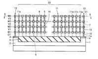
- a semiconductor deviceincludes a semiconductor substrate 1 having a main surface 1 a , a plurality of interconnections 11 formed in a capacitance forming region 22 on main surface 1 a , a plurality of interconnections 12 formed outside of capacitance forming region 22 , and an insulating layer 5 formed on main surface 1 a and filling in between each of interconnections 11 and 12 .
- Interconnections 11 and 12are formed for example of a metal such as copper (Cu) or aluminum (Al), polysilicon, or the like.
- Insulating layer 5is formed for example of TEOS (tetra ethyl ortho silicate), BPTEOS, FSG (F-doped silicate glass), or a silicon oxide film or a silicon nitride film doped with a predetermined concentration of phosphorus (P) or boron (B).
- TEOStetra ethyl ortho silicate
- BPTEOSBPTEOS
- FSGF-doped silicate glass
- Pphosphorus
- Bboron
- a p well 2is formed with a predetermined depth from main surface 1 a .
- an isolating oxide film 3is formed in p well 2 .
- an active region 4 connected to a ground potentialis formed with a predetermined depth on either side of isolating oxide film 3 .
- Isolating oxide film 3extends below capacitance forming region 22 in which the plurality of interconnections 11 are formed, and active region 4 extends below the plurality of interconnections 12 .
- Interconnections 11 and 12are formed in a plane 21 extending parallel to main surface 1 a at a position apart from main surface 1 a .
- a plurality of planes 21are defined at equal intervals (hereinafter, layers in which the plurality of planes 21 are defined will be referred to as an M (metal) 1 layer, an M 2 layer, an M 3 layer, respectively, in order of closeness to main surface 1 a , a space between main surface 1 a and M 1 layer will be referred to as a CT (contact) layer, and spaces between vertically adjacent M layers will be referred to as a V (via hole) 1 layer, a V 2 layer, a V 3 layer, respectively).
- Interconnections 11 and 12are formed in each of M 1 layer to M 4 layer such that, when main surface 1 a is viewed from the front of FIG. 2 , they are seen overlying each other on main surface 1 a.
- Each of the plurality of interconnections 11extends in plane 21 in a predetermined direction (a direction shown by an arrow 23 in FIG. 2 ).
- the plurality of interconnections 11align each other at equal intervals in a direction orthogonal to the direction in which interconnections 11 extend (a direction shown by an arrow 24 in FIG. 2 ).
- interconnections 15 and 16are formed apart from each other to extend in the direction shown by arrow 24 , between active regions 4 formed on both sides of isolating oxide film 3 .
- the plurality of interconnections 11include a plurality of interconnections 11 n branched from interconnection 15 and extending toward interconnection 16 , and a plurality of interconnections 11 m branched from interconnection 16 and extending toward interconnection 15 .
- Interconnections 11 m and 11 nare arranged in such a manner that the teeth of two combs face each other in an interdigitated pattern.
- Each of the plurality of interconnections 12extends in plane 21 in the same direction as the direction in which the plurality of interconnections 11 extend.
- the plurality of interconnections 12are formed adjacent to interconnections 11 p of the plurality of interconnections 11 located at the edges of capacitance forming region 22 . That is, the plurality of interconnections 12 are positioned at both ends of the plurality of interconnections 11 in the direction in which interconnections 11 align.
- the distance between interconnection 11 p and interconnection 12is the same as the distance between neighboring interconnections 11 .
- interconnections 11 and 12 in vertically adjacent layersare connected by via holes 14 and 13 , respectively, formed in V 1 layer to V 3 layer. Note that, in FIG. 2 , via holes 14 and 13 formed in V 3 layer are shown by dashed lines. Further, interconnection 12 formed in M 1 layer and active region 4 formed in main surface 1 a are connected by a contact 10 formed in CT layer. Interconnections 15 and 16 in vertically adjacent layers are connected by via holes 17 formed in V 1 layer to V 3 layer.
- the plurality of interconnections 11 mare at the same potential, having a potential drawn from a predetermined position of interconnection 16 in M 4 layer
- the plurality of interconnections 11 nare at the same potential, having a potential drawn from a predetermined position of interconnection 15 in M 4 layer.
- an interconnection capacitance 8 using insulating layer 5 as a dielectric layeris formed between interconnections 11 m and 11 n adjacent to each other in each plane 21 defined in M 1 layer to M 4 layer.
- interconnections 11 m and 11 ncan be set at respective predetermined potentials all at once by arranging them in the form of two combs.
- interconnection capacitance 8having a greater capacitance value can be formed in a limited region on main surface 1 a . Further, since the plurality of interconnections 11 are arranged to align in the direction orthogonal to their extending direction, the distance between which interconnections 11 are adjacent to each other in that direction can be set longer, achieving a greater capacitance value.
- the plurality of interconnections 12are connected via active regions 4 to p well 2 at a ground potential, they are fixed at the ground potential.
- the plurality of interconnections 12act as a shield for capacitance forming region 22 , playing a role to block electrical interference (noise) from an external circuit provided around capacitance forming region 22 .
- the plurality of interconnections 12are arranged at the both ends of the plurality of interconnections 11 , noise from the external circuit provided on either side of capacitance forming region 22 can surely be blocked.
- parasitic capacitances 6 formed between main surface 1 a of semiconductor substrate 1 and the plurality of interconnections 11 provided in M 1 layer, and parasitic capacitances 7 formed between the plurality of interconnections 11 p and the plurality of interconnections 12are shown by dotted lines.
- the semiconductor device in the first embodiment of the present inventionincludes semiconductor substrate 1 having main surface 1 a ; a plurality of interconnections 11 as first interconnections formed in capacitance forming region 22 defined on main surface 1 a and extending in a predetermined direction; insulating layer 5 formed on main surface 1 a and filling in between each of the plurality of interconnections 11 ; and a plurality of interconnections 12 as second interconnections adjacent to interconnections 11 p as the first interconnections arranged at the edges of capacitance forming region 22 , extending in a predetermined direction, and having a fixed potential.
- Interconnections 111 and 12are arranged at substantially equal intervals in plane 21 as a first plane parallel to main surface 1 a.
- Interconnections 11 and 12are arranged to align in a direction substantially perpendicular to the predetermined direction.
- the plurality of interconnections 12are provided at both ends of the plurality of interconnections 11 arranged in plane 21 .
- Interconnections 11 and 12are formed in a plurality of planes 21 spaced with each other.
- main surface 1 a of p-type semiconductor substrate 1when main surface 1 a of p-type semiconductor substrate 1 is provided with a p well for example, the p well may be fixed at a ground potential, and when main surface 1 a is provided with an n well, the n well may be fixed at a power supply potential and semiconductor substrate 1 may be fixed at a ground potential. Furthermore, when main surface 1 a of n-type semiconductor substrate 1 is provided with an n well, the n well may be fixed at a power supply potential, and when main surface 1 a is provided with a p well, the p well may be fixed at a ground potential and semiconductor substrate 1 may be fixed at a power supply potential.
- the plurality of interconnections 11 constituting interconnection capacitance 8 and the plurality of interconnections 12 acting as a shieldare formed at equal intervals.
- uneven arrangement of the interconnectionswill not be caused between the central portion and the end portion of capacitance forming region 22 in plane 21 . Therefore, when forming interconnections 11 and 12 , etching progresses at a uniform rate anywhere in capacitance forming region 22 , ensuring a uniform finished configuration.
- the plurality of interconnections 12are at a fixed potential, the influence of noise from an external circuit exerted on interconnection capacitance 8 can be reduced.
- the plurality of interconnections 12serve as a dummy element allowing for a uniform process and also as a shield for blocking external noise.
- interconnection capacitance 8having no fluctuations in a capacitance value and offering a desired characteristic can be formed.
- a semiconductor device in a second embodiment of the present inventionbasically has a configuration similar to that of the semiconductor device in the first embodiment.
- description of identical partswill not be repeated.
- the cross section along the line IV-IV in FIG. 6has a configuration identical to that of the cross section shown in FIG. 4 .
- via holes 13 formed in V 3 layerare shown by dashed lines.
- the plurality of interconnections 11 in vertically adjacent layersare not connected by a via hole, and insulating layer 5 is filled therebetween.
- the plurality of interconnections 11are formed such that, when main surface 1 a is viewed from the front of FIG. 6 , interconnections 11 formed in M 1 layer and M 3 layer are seen overlying each other on main surface 1 a , and interconnections 11 formed in M 2 layer and M 4 layer are seen overlying each other on main surface 1 a.
- M 1 layer and M 3 layerare provided with interconnections 11 m branched from interconnection 16 formed in each layer and extending toward interconnection 15 .
- M 2 layer and M 4 layerare provided with interconnections 11 n branched from interconnection 15 formed in each layer and extending toward interconnection 16 . That is, in the present embodiment, interconnections 11 m and 11 n are arranged in such a manner that the teeth of two combs face each other in an interdigitated pattern in plane 21 as well as in a plane orthogonal to plane 21 .
- an interconnection capacitance 8 ais formed between interconnections 11 m and 11 n adjacent to each other in plane 21
- an interconnection capacitance 8 bis also formed between interconnections 11 m and 11 n in vertically adjacent layers.
- a semiconductor device in a third embodiment of the present inventionbasically has a configuration similar to that of the semiconductor device in the first embodiment. Hereinafter, description of identical parts will not be repeated.
- semiconductor substrate 1 of the present embodimentincludes an n well 34 formed on either side of p well 2 .
- P well 2is formed to be located immediately below interconnections 11 and 12 in a lateral direction and a depth direction of the plane of FIG. 8 .
- an n + well 31is formed at a predetermined depth from main surface 1 a .
- N + well 31is formed all over the position underlying n wells 34 and p well 2 in the lateral direction and the depth direction of the plane of FIG. 8 .
- N + well 31extends parallel to n wells 34 and p well 2 .
- p well 2When p well 2 is not used to fix the plurality of interconnections 12 at a potential, p well 2 is only necessary to underlie at least a region over which, when viewed from above, capacitance forming region 22 is seen on main surface 1 a in the lateral direction and the depth direction of the plane of FIG. 8 . Similarly, n + well 31 is only necessary to underlie at least all the region over which, when viewed from above, capacitance forming region 22 is seen on main surface 1 a.
- isolating oxide film 3is formed at a boundary between n well 34 and p well 2 , and active region 4 is further formed on n well 34 .
- Active region 4is connected via contact 10 to an interconnection 33 formed on main surface 1 a and fixed at a power supply potential. With this configuration, n + well 31 is fixed at the power supply potential.
- the effect similar to that described in the first embodimentcan be obtained.
- semiconductor substrate 1 with n + well 31 having a fixed potentialnoise transmitted mainly from a rear side of semiconductor substrate 1 to capacitance forming region 22 can be blocked effectively.
- the effect similar to that obtained by n + well 31can also be achieved by p well 2 having a fixed potential.
- a semiconductor device in a fourth embodiment of the present invention shown in FIGS. 9 to 12basically has a configuration similar to those of the semiconductor devices in the first and the third embodiments. Hereinafter, description of identical parts will not be repeated.
- via hole 13 formed in V 4 layeris shown by a dashed line.
- a plane 37 extending parallel to main surface 1 ais defined at a position of an M 5 layer spaced from M 4 layer by a predetermined interval therebetween.
- Plane 37is defined such that capacitance forming region 22 is located between plane 37 and main surface 1 a .
- Plane 37is provided with a plurality of interconnections 38 .
- the plurality of interconnections 38extend in plane 37 in a direction identical to the direction in which the plurality of interconnections 11 extend (a direction shown by arrow 23 in FIG. 10 ).
- the plurality of interconnections 38align each other at equal intervals in a direction orthogonal to the direction in which interconnections 38 extend (a direction shown by arrow 24 in FIG. 10 ).
- interconnections 41 and 42are formed apart from each other to extend in the direction shown by arrow 24 .
- the plurality of interconnections 38include a plurality of interconnections 38 n branched from interconnection 41 and extending toward interconnection 42 , and a plurality of interconnections 38 m branched from interconnection 42 and extending toward interconnection 41 , and interconnections 38 m and 38 n are arranged in such a manner that the teeth of two combs face each other in an interdigitated pattern.
- Interconnections 38 m and 38 nare formed such that, when main surface 1 a is viewed from the front of FIG. 10 , they are seen in overlying relation with interconnections 11 m , 11 n and interconnections 12 on main surface 1 a.
- Interconnection 12 formed in M 4 layer and interconnection 38 formed in M 5 layer above interconnection 12are connected by via hole 13 . With this configuration, interconnections 12 and 38 are fixed at a ground potential.
- a parasitic capacitance 39 formed between interconnection 38 in M 5 layer and interconnection 11 in M 4 layeris shown by a dotted line.
- the effect similar to those described in the first and the third embodimentscan be obtained.
- the plurality of interconnections 38 covering capacitance forming region 22 from aboveact as a shield together with the plurality of interconnections 12 , noise from an external circuit can be blocked further reliably.
- a semiconductor device in a fifth embodiment of the present inventionbasically has a configuration similar to that of the semiconductor device in the fourth embodiment.
- description of identical partswill not be repeated.
- interconnections lp located at a position adjacent to the plurality of interconnections 12 having a fixed potentialare connected to a low impedance node. More specifically, the plurality of interconnections 11 m including interconnections 11 p in FIG. 13 are connected to a relatively low impedance node, and the plurality of interconnections 1 in not including interconnections 11 p are connected to a relatively high impedance node.
- the effect similar to that described in the fourth embodimentcan be obtained.
- the plurality of interconnections lpare connected to a relatively low impedance node, the influence of parasitic capacitance 7 formed between interconnection 11 p and interconnection 12 can be reduced.
- a circuit using interconnection capacitance 8can be implemented with higher accuracy, preventing parasitic capacitance 7 from causing deviation of a capacitance value ratio in interconnection capacitance 8 or deviation from a desired transmissibility when interconnection capacitance 8 is utilized in an integrator using an amplifier.
- a semiconductor device in a sixth embodiment of the present inventionbasically has a configuration similar to that of the semiconductor device in the fourth embodiment. Hereinafter, description of identical parts will not be repeated.
- interconnections 38 formed in M 5 layer and connected by via holes 13 to interconnections 12 having a fixed potential and interconnections 11 m formed in M 5 layer and connected by via holes 14 to interconnections 11 m formed in M 4 layerare provided in an interdigitated pattern.
- the plurality of interconnections 11 minclude interconnections 11 p formed at a position adjacent to the plurality of interconnections 12 having a fixed potential (i.e., at a position surrounded by a chain double-dashed line 51 ).
- the plurality of interconnections 11 mare connected to a relatively low impedance node, and the plurality of interconnections 11 n are connected to a relatively high impedance node.
- interconnections 38 having a fixed potentialcan be used as a shield for capacitance forming region 22 , and the influence due to parasitic capacitance 7 can also be reduced as in the effect described in the fifth embodiment.
- a semiconductor device in a seventh embodiment of the present inventionbasically has a configuration similar to that of the semiconductor device in the fourth embodiment. Hereinafter, description of identical parts will not be repeated.
- a plurality of floating interconnections 57 spaced from each otherare formed at a position in M 4 layer sandwiched between interconnections 12 at both ends (i.e., at a position surrounded by a chain double-dashed line 56 ).
- the plurality of floating interconnections 57extend in a depth direction of the plane of FIG. 15 .
- Floating interconnection 57is completely surrounded by insulating layer 5 , and has a floating potential. More specifically, floating interconnection 57 at a floating potential is positioned between interconnection 38 formed in M 5 layer and having a fixed potential and interconnection 11 formed in M 3 layer.
- a semiconductor device in an eighth embodiment of the present inventionbasically has a configuration similar to that of the semiconductor device in the fourth embodiment. Hereinafter, description of identical parts will not be repeated.
- a plurality of floating interconnections 59 spaced from each otherare formed at a position in M 1 layer sandwiched between interconnections 12 at both ends (i.e., at a position surrounded by a chain double-dashed line 58 ).
- the plurality of floating interconnections 59extend in a depth direction of the plane of FIG. 16 .
- Floating interconnection 59is completely surrounded by insulating layer 5 , and has a floating potential. More specifically, floating interconnection 59 at a floating potential is positioned between interconnection 11 formed in M 2 layer and main surface 1 a of semiconductor substrate 1 .
- a semiconductor device in a ninth embodiment of the present inventionbasically has a configuration similar to that of the semiconductor device in the fourth embodiment. Hereinafter, description of identical parts will not be repeated.
- a plurality of floating interconnections 61are formed at a position adjacent to the plurality of interconnections 12 in M 1 layer to M 4 layer (i.e., at a position surrounded by a chain double-dashed line 60 ).
- the plurality of floating interconnections 61extend in a depth direction of the plane of FIG. 17 .
- Floating interconnection 61is completely surrounded by insulating layer 5 , and has a floating potential. More specifically, floating interconnection 61 at a floating potential is positioned between interconnection 11 p formed in each of M 1 to M 4 layers and interconnection 12 having a fixed potential.
- a semiconductor device in a tenth embodiment of the present inventionbasically has a configuration similar to that of the semiconductor device in the fourth embodiment. Hereinafter, description of identical parts will not be repeated.
- no interconnectionsare provided in a position in M 4 layer sandwiched between interconnections 12 at both ends (i.e., at a position surrounded by a chain double-dashed line 63 ), and the position is filled with insulating layer 5 .
- the distance from interconnection 38 formed in M 5 layer to interconnection 11 adjacent to interconnection 38is greater than the distance between vertically adjacent interconnections 11 .
- a semiconductor device in an eleventh embodiment of the present inventionbasically has a configuration similar to that of the semiconductor device in the seventh embodiment. Hereinafter, description of identical parts will not be repeated.
- a plurality of floating interconnections 57are formed at a position in M 4 layer sandwiched between interconnections 12 at both ends, corresponding to every other interconnection 11 therebelow.
- the plurality of floating interconnections 57are not provided at a portion in which a parasitic capacitance may lead to deterioration of circuit accuracy (i.e., a portion to be a high impedance node when a circuit is implemented), and provided at a portion to be a low impedance node.
- the semiconductor device with such a configurationdeterioration of accuracy in a high impedance node due to a parasitic capacitance can further be reduced as compared to the semiconductor device in the seventh embodiment. Furthermore, even in M 4 layer in which floating interconnections 57 are thinned out compared to the case of FIG. 15 , the area occupied by the interconnections is larger than in the case shown in FIG. 18 , enabling to form more planar M 5 layer on M 4 layer.
- a semiconductor device in a twelfth embodiment of the present inventionbasically has a configuration similar to that of the semiconductor device in the fourth embodiment. Hereinafter, description of identical parts will not be repeated.
- no interconnectionsare provided in a position in M 1 layer sandwiched between interconnections 12 at both ends (i.e., at a position surrounded by a chain double-dashed line 66 ), and the position is filled with insulating layer 5 .
- the distance from main surface 1 a of semiconductor substrate 1 to interconnection 11 adjacent to main surface 1 ais greater than the distance between vertically adjacent interconnections 11 .
- a semiconductor device in a thirteenth embodiment of the present inventionbasically has a configuration similar to that of the semiconductor device in the eighth embodiment. Hereinafter, description of identical parts will not be repeated.
- a plurality of floating interconnections 59are formed at a position in M 1 layer sandwiched between interconnections 12 at both ends, corresponding to every other interconnection 11 therebelow.
- Floating interconnections 59are not provided at a portion in which a parasitic capacitance may lead to deterioration of circuit accuracy (i.e., a portion to be a high impedance node when a circuit is implemented), and provided at a portion to be a low impedance node.
- the semiconductor device with such a configurationdeterioration of accuracy in a high impedance node due to a parasitic capacitance can further be reduced as compared to the semiconductor device in the eighth embodiment. Furthermore, even in M 1 layer in which floating interconnections 59 are thinned out compared to the case of FIG. 16 , the area occupied by the interconnections is larger than in the case shown in FIG. 20 , enabling to form more planar M 2 layer on M 1 layer.
- a semiconductor device in a fourteenth embodiment of the present inventionbasically has a configuration similar to that of the semiconductor device in the fourth embodiment. Hereinafter, description of identical parts will not be repeated.
- via hole 13 formed in V 4 layeris shown by a dashed line.
- the area ratio of active region 4 to a region 71 on main surface 1 a immediately above which interconnections 111 and 12 are formedsatisfies a predetermined occupied area ratio.
- a “predetermined occupied area ratio”refers to an area ratio of a specific region defined to produce planar main surface 1 a through the manufacturing process of a semiconductor device (including an active region formed by introducing impurities into main surface 1 a , and a region in which a polysilicon film is formed in contact with main surface 1 a ).
- the predetermined occupied area ratiois, for example, not less than 25%, not less than 50%, or not less than 75%.
- the semiconductor device in the fourteenth embodiment of the present inventionincludes active region 4 as the specific region defined in main surface 1 a .
- the area ratio of active region 4 to region 71 on main surface 1 a immediately above which interconnections 11 and 12 are formedis not less than a predetermined value.
- a planar film(insulating layer 5 in the present embodiment) can be formed on main surface 1 a . Accordingly, interconnections 11 and 12 can be formed on the planar film, and thus interconnections 11 and 12 can be finished in a more uniform configuration.
- a semiconductor device in a fifteenth embodiment of the present inventionbasically has a configuration similar to that of the semiconductor device in the fourteenth embodiment. Hereinafter, description of identical parts will not be repeated.
- isolating oxide film 3is additionally formed at a position in main surface 1 a in which active region 4 has been formed in FIG. 22 .
- Isolating oxide film 3is located immediately below interconnection 11 n having relatively high impedance.
- active region 4is located immediately below interconnection 11 m having relatively low impedance.
- the semiconductor device with such a configurationthe effect similar to that described in the fourteenth embodiment can be obtained.
- the influence of parasitic capacitance 6 formed between main surface 1 a and interconnection 11 n connected to a high impedance nodecan be reduced.
- a semiconductor device in a sixteenth embodiment of the present inventionbasically has a configuration similar to that of the semiconductor device in the fifteenth embodiment. Hereinafter, description of identical parts will not be repeated.
- a polysilicon film 73is formed immediately below interconnection 11 m having relatively low impedance, and isolating oxide film 3 is formed immediately below interconnection 11 n having relatively high impedance.
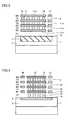
- a semiconductor device 83has a configuration in which drawing terminal cells 80 and 81 and a unit capacitance cell 82 located between drawing terminal cells 80 and 81 are combined in a Y direction.
- Drawing terminal cells 80 and 81include the interconnection configuration of interconnections 41 and 42 in the semiconductor device shown in FIG. 10
- unit capacitance cell 82includes the interconnection configuration having a predetermined width between interconnection 41 and interconnection 42 .
- the length of drawing terminal cells 80 and 81 and unit capacitance cell 82 in an X directionis determined to satisfy the predetermined occupied area ratio described in the fourteenth embodiment.
- FIGS. 27 to 30show variations of the semiconductor device in FIG. 26 .
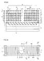
- a semiconductor device 84has a configuration in which drawing terminal cells 80 and 81 and two unit capacitance cells 82 located between drawing terminal cells 80 and 81 are combined in the Y direction.
- a semiconductor device 85has a configuration in which drawing terminal cells 80 and 81 and 10 unit capacitance cells 82 located between drawing terminal cells 80 and 81 are combined in the Y direction.
- a semiconductor device 86has a configuration in which four semiconductor devices 85 shown in FIG. 28 are connected in parallel, and a polysilicon layer 87 extending in a band shape is located on its either side.
- Polysilicon layer 87is provided to guarantee a sufficient occupied area ratio in such a case where there is no gate layer in the periphery of the capacitance forming region.
- a semiconductor device 90has a configuration substantially similar to that of semiconductor device 86 in FIG. 29 , except that two polysilicon layers 88 , extending in a band shape and divided in the middle, are located on its either side. Polysilicon layers 88 divided to have an appropriate size are used when polysilicon layer 87 shown in FIG. 29 would provide too high an occupied area ratio.
- a method of designing the semiconductor device in the seventeenth embodiment of the present inventionutilizes the semiconductor devices described in the fourteenth to the sixteenth embodiments.
- the method of designing the semiconductor deviceincludes the steps of unitizing the semiconductor device as a unit capacitance cell, and combining a plurality of such unit capacitance cells.
- the semiconductor devicesince the cells satisfying a predetermined occupied area ratio are combined to determine the configuration of the semiconductor device, the semiconductor device also always satisfies the predetermined occupied area ratio as a whole. This makes it possible to design a semiconductor device satisfying a predetermined occupied area ratio without going through a complicated design process. With this method, a semiconductor device having an interconnection capacitance with small fluctuations during processing can be obtained.
- a semiconductor device having a capacitive element for which external electrical interference is sufficiently reduced and offering a desired characteristiccan be provided.
Landscapes
- Engineering & Computer Science (AREA)
- Power Engineering (AREA)
- Physics & Mathematics (AREA)
- Condensed Matter Physics & Semiconductors (AREA)
- General Physics & Mathematics (AREA)
- Computer Hardware Design (AREA)
- Microelectronics & Electronic Packaging (AREA)
- Semiconductor Integrated Circuits (AREA)
- Design And Manufacture Of Integrated Circuits (AREA)
- Internal Circuitry In Semiconductor Integrated Circuit Devices (AREA)
Abstract
Description
- 1. Field of the Invention
- The present invention relates to a semiconductor device, and more particularly, to a semiconductor device having a capacitive element utilizing an interconnection layer.
- 2. Description of the Background Art
- Recently, capacitive elements utilizing a parasitic capacitance between interconnections have started to be used along with process miniaturization. A semiconductor integrated circuit device having such a capacitive element is disclosed for example in Japanese Patent Laying-Open No. 2001-177056. The semiconductor integrated circuit device disclosed in Japanese Patent Laying-Open No. 2001-177056 includes a first electrode, a second electrode, and a dielectric film sandwiched between the first and the second electrodes, constituting a capacitive element. The first electrodes and the second electrodes are arranged to face each other in a plane direction and a thickness direction of a semiconductor substrate.
- Japanese Patent Laying-Open No. 2002-100732 discloses a method of forming a capacitive element in which at least two interconnections formed in an identical interconnection layer are arranged in proximity to each other to obtain an interconnection capacitance serving as a capacitive element.
- Further, Japanese Patent Laying-Open No. 2003-152085 discloses a semiconductor device for preventing noise coupling to an MIM (Metal-Insulator-Metal) capacitance and a method of manufacturing the same. The semiconductor device disclosed in Japanese Patent Laying-Open No. 2003-152085 includes a semiconductor substrate, a capacitive element formed above the semiconductor substrate, and at least a shield layer formed above or below the capacitive element. In another semiconductor device, a stacked film electrically connected to the shield layer is formed in the same layer as the capacitive element to cause the stacked film to operate similarly to the shield layer.
- Furthermore, a capacitive element utilizing an interlayer capacitance between interconnection layers is disclosed in “Capacity Limits and Matching Properties of Integrated Capacitors” by Robert Aparicio et al., IEEE Journal of Solid-state Circuits, Vol. 37, No. 3, March 2002, pp. 384-393.
- However, the semiconductor integrated circuit device disclosed in Japanese Patent Laying-Open No. 2001-177056 and the method of forming a capacitive element disclosed in Japanese Patent Laying-Open No. 2002-100732 do not include a measure to reduce interference with the capacitive element by an external circuit. Consequently, there arises a problem that the capacitance of the capacitive element fluctuates. Particularly, as an external circuit such as a digital portion progresses to operate faster, the measure against such a problem is increasingly required.
- Further, in the semiconductor integrated circuit device or the like disclosed in Japanese Patent Laying-Open Nos. 2001-177056, 2002-100732 and 2003-152085, if interconnection layers and silicon gate layers are arranged with uneven density, the unevenness will cause a difference in the progress of etching. Thus, the configuration obtained at the end of the process may have a non-uniform finish. Furthermore, if an active region and the like formed in a main surface of the semiconductor substrate does not have an area satisfying a predetermined ratio to a fixed region on the main surface, it is not possible to form a layer uniformly over the main surface. Thus, it becomes difficult to control etching appropriately when forming a capacitive element on the film. For these reasons, it is not possible to form a capacitive element offering a desired characteristic.
- To solve the problems described above, an object of the present invention is to provide a semiconductor device having a capacitive element for which external electrical interference is sufficiently reduced and offering a desired characteristic.
- The semiconductor device according to the present invention includes a semiconductor substrate including a main surface; a plurality of first interconnections formed in a capacitance forming region defined on the main surface and extending in a predetermined direction; a plurality of second interconnections each adjacent to one of the first interconnections located at an edge of the capacitance forming region, extending in the predetermined direction, and having a fixed potential; and an insulating layer formed on the main surface and filling in between each of the plurality of first interconnections and between the first interconnection and the second interconnection adjacent to each other. The plurality of first interconnections and the plurality of second interconnections are located at substantially equal intervals in a first plane parallel to the main surface, and located to align in a direction substantially perpendicular to the predetermined direction.
- The foregoing and other objects, features, aspects and advantages of the present invention will become more apparent from the following detailed description of the present invention when taken in conjunction with the accompanying drawings.
FIG. 1 is a cross-sectional view of a semiconductor device in a first embodiment of the present invention.FIG. 2 is a plan view of the semiconductor device taken along the arrowed line II-II inFIG. 1 .FIG. 3 is a cross-sectional view taken along the line III-II inFIG. 2 .FIG. 4 is a cross-sectional view taken along the line IV-IV inFIG. 2 .FIG. 5 is a cross-sectional view showing a semiconductor device in a second embodiment of the present invention.FIG. 6 is a plan view of the semiconductor device taken along the arrowed line VI-VI inFIG. 5 .FIG. 7 is a cross-sectional view taken along the line VII-VII inFIG. 6 .FIG. 8 is a cross-sectional view showing a semiconductor device in a third embodiment of the present invention.FIG. 9 is a cross-sectional view showing a semiconductor device in a fourth embodiment of the present invention.FIG. 10 is a plan view of the semiconductor device taken along the arrowed line X-X inFIG. 9 .FIG. 11 is a cross-sectional view taken along the line XI-XI inFIG. 10 .FIG. 12 is a cross-sectional view taken along the line XII-XII inFIG. 10 .- FIGS.13 to22 are cross-sectional views showing semiconductor devices in fifth to fourteenth embodiments of the present invention, respectively.
FIG. 23 is a plan view of the semiconductor device taken along the arrowed line XXIII-XXIII inFIG. 22 .FIGS. 24 and 25 are cross-sectional views showing semiconductor devices in fifteenth and sixteenth embodiments of the present invention, respectively.FIG. 26 is a plan view showing a semiconductor device manufactured according to a method of designing a semiconductor device in a seventeenth embodiment of the present invention.- FIGS.27 to30 are plan views showing variations of the semiconductor device shown in
FIG. 26 . - Embodiments of the present invention will now be described with reference to the drawings.
- Referring to
FIGS. 1 and 2 , a semiconductor device according to a first embodiment of the present invention includes asemiconductor substrate 1 having amain surface 1a, a plurality ofinterconnections 11 formed in acapacitance forming region 22 onmain surface 1a, a plurality ofinterconnections 12 formed outside ofcapacitance forming region 22, and aninsulating layer 5 formed onmain surface 1aand filling in between each ofinterconnections Interconnections layer 5 is formed for example of TEOS (tetra ethyl ortho silicate), BPTEOS, FSG (F-doped silicate glass), or a silicon oxide film or a silicon nitride film doped with a predetermined concentration of phosphorus (P) or boron (B). - In p-
type semiconductor substrate 1,a p well 2 is formed with a predetermined depth frommain surface 1a. Inmain surface 1aofsemiconductor substrate 1, anisolating oxide film 3 is formed inp well 2. Further, inmain surface 1a, anactive region 4 connected to a ground potential is formed with a predetermined depth on either side of isolatingoxide film 3. Isolatingoxide film 3 extends belowcapacitance forming region 22 in which the plurality ofinterconnections 11 are formed, andactive region 4 extends below the plurality ofinterconnections 12. Interconnections plane 21 extending parallel tomain surface 1aat a position apart frommain surface 1a. A plurality ofplanes 21 are defined at equal intervals (hereinafter, layers in which the plurality ofplanes 21 are defined will be referred to as an M (metal)1 layer, an M2 layer, an M3 layer, respectively, in order of closeness tomain surface 1a, a space betweenmain surface 1aand M1 layer will be referred to as a CT (contact) layer, and spaces between vertically adjacent M layers will be referred to as a V (via hole)1 layer, a V2 layer, a V3 layer, respectively).Interconnections main surface 1ais viewed from the front ofFIG. 2 , they are seen overlying each other onmain surface 1a.- Each of the plurality of
interconnections 11 extends inplane 21 in a predetermined direction (a direction shown by anarrow 23 inFIG. 2 ). The plurality ofinterconnections 11 align each other at equal intervals in a direction orthogonal to the direction in whichinterconnections 11 extend (a direction shown by anarrow 24 inFIG. 2 ). - In
plane 21,interconnections arrow 24, betweenactive regions 4 formed on both sides of isolatingoxide film 3. The plurality ofinterconnections 11 include a plurality ofinterconnections 11nbranched frominterconnection 15 and extending towardinterconnection 16, and a plurality ofinterconnections 11mbranched frominterconnection 16 and extending towardinterconnection 15.Interconnections - Each of the plurality of
interconnections 12 extends inplane 21 in the same direction as the direction in which the plurality ofinterconnections 11 extend. The plurality ofinterconnections 12 are formed adjacent tointerconnections 11pof the plurality ofinterconnections 11 located at the edges ofcapacitance forming region 22. That is, the plurality ofinterconnections 12 are positioned at both ends of the plurality ofinterconnections 11 in the direction in which interconnections11 align. The distance betweeninterconnection 11pandinterconnection 12 is the same as the distance between neighboringinterconnections 11. - Referring to FIGS.1 to4,
interconnections holes FIG. 2 , viaholes interconnection 12 formed in M1 layer andactive region 4 formed inmain surface 1aare connected by acontact 10 formed in CT layer.Interconnections holes 17 formed in V1 layer to V3 layer. - With the configuration described above, the plurality of
interconnections 11mare at the same potential, having a potential drawn from a predetermined position ofinterconnection 16 in M4 layer, and the plurality ofinterconnections 11nare at the same potential, having a potential drawn from a predetermined position ofinterconnection 15 in M4 layer. Thus, by providing a potential difference betweeninterconnections interconnection capacitance 8 using insulatinglayer 5 as a dielectric layer is formed betweeninterconnections plane 21 defined in M1 layer to M4 layer. Although a large number ofinterconnections 11 are formed,interconnections - In this case, by forming the plurality of
interconnections 11 in the plurality ofplanes 21,interconnection capacitance 8 having a greater capacitance value can be formed in a limited region onmain surface 1a. Further, since the plurality ofinterconnections 11 are arranged to align in the direction orthogonal to their extending direction, the distance between which interconnections11 are adjacent to each other in that direction can be set longer, achieving a greater capacitance value. - Furthermore, since the plurality of
interconnections 12 are connected viaactive regions 4 to p well2 at a ground potential, they are fixed at the ground potential. Thus, the plurality ofinterconnections 12 act as a shield forcapacitance forming region 22, playing a role to block electrical interference (noise) from an external circuit provided aroundcapacitance forming region 22. In this case, since the plurality ofinterconnections 12 are arranged at the both ends of the plurality ofinterconnections 11, noise from the external circuit provided on either side ofcapacitance forming region 22 can surely be blocked. - Note that, in
FIG. 1 ,parasitic capacitances 6 formed betweenmain surface 1aofsemiconductor substrate 1 and the plurality ofinterconnections 11 provided in M1 layer, andparasitic capacitances 7 formed between the plurality ofinterconnections 11pand the plurality ofinterconnections 12 are shown by dotted lines. - As described above, the semiconductor device in the first embodiment of the present invention includes
semiconductor substrate 1 havingmain surface 1a; a plurality ofinterconnections 11 as first interconnections formed incapacitance forming region 22 defined onmain surface 1aand extending in a predetermined direction; insulatinglayer 5 formed onmain surface 1aand filling in between each of the plurality ofinterconnections 11; and a plurality ofinterconnections 12 as second interconnections adjacent tointerconnections 11pas the first interconnections arranged at the edges ofcapacitance forming region 22, extending in a predetermined direction, and having a fixed potential.Interconnections 111 and12 are arranged at substantially equal intervals inplane 21 as a first plane parallel tomain surface 1a. Interconnections interconnections 12 are provided at both ends of the plurality ofinterconnections 11 arranged inplane 21.Interconnections planes 21 spaced with each other.- Although the description has been given in the present embodiment on the case where the plurality of
interconnections 12 are fixed at a ground potential, the plurality ofinterconnections 12 may be fixed for example at a power supply potential, depending on the type of the well at the bottom. Further, although the description has been given on the case where the plurality ofplanes 21 are defined at equal intervals with each other, for example the distance between M1 layer and M2 layer may be different from the distance between M2 layer and M3 layer. Furthermore, although the description has been given on the case whereinterconnections interconnections - Further, when
main surface 1aof p-type semiconductor substrate 1 is provided with a p well for example, the p well may be fixed at a ground potential, and whenmain surface 1ais provided with an n well, the n well may be fixed at a power supply potential andsemiconductor substrate 1 may be fixed at a ground potential. Furthermore, whenmain surface 1aof n-type semiconductor substrate 1 is provided with an n well, the n well may be fixed at a power supply potential, and whenmain surface 1ais provided with a p well, the p well may be fixed at a ground potential andsemiconductor substrate 1 may be fixed at a power supply potential. - According to the semiconductor device with the configuration described above, the plurality of
interconnections 11 constitutinginterconnection capacitance 8 and the plurality ofinterconnections 12 acting as a shield are formed at equal intervals. Thus, uneven arrangement of the interconnections will not be caused between the central portion and the end portion ofcapacitance forming region 22 inplane 21. Therefore, when forminginterconnections capacitance forming region 22, ensuring a uniform finished configuration. Further, since the plurality ofinterconnections 12 are at a fixed potential, the influence of noise from an external circuit exerted oninterconnection capacitance 8 can be reduced. That is, in the present embodiment, the plurality ofinterconnections 12 serve as a dummy element allowing for a uniform process and also as a shield for blocking external noise. For the reasons described above,interconnection capacitance 8 having no fluctuations in a capacitance value and offering a desired characteristic can be formed. - A semiconductor device in a second embodiment of the present invention basically has a configuration similar to that of the semiconductor device in the first embodiment. Hereinafter, description of identical parts will not be repeated.
- Of FIGS.5 to7 showing the semiconductor device of the present embodiment, the cross section along the line IV-IV in
FIG. 6 has a configuration identical to that of the cross section shown inFIG. 4 . InFIG. 6 , viaholes 13 formed in V3 layer are shown by dashed lines. - Referring to FIGS.5 to7, in the present embodiment; the plurality of
interconnections 11 in vertically adjacent layers are not connected by a via hole, and insulatinglayer 5 is filled therebetween. The plurality ofinterconnections 11 are formed such that, whenmain surface 1ais viewed from the front ofFIG. 6 ,interconnections 11 formed in M1 layer and M3 layer are seen overlying each other onmain surface 1a, andinterconnections 11 formed in M2 layer and M4 layer are seen overlying each other onmain surface 1a. - For example, when a cross section along the line VII-VII in
FIG. 6 is viewed inFIG. 7 , M1 layer and M3 layer are provided withinterconnections 11mbranched frominterconnection 16 formed in each layer and extending towardinterconnection 15. M2 layer and M4 layer are provided withinterconnections 11nbranched frominterconnection 15 formed in each layer and extending towardinterconnection 16. That is, in the present embodiment,interconnections plane 21 as well as in a plane orthogonal to plane21. - With this configuration, in the present embodiment, an interconnection capacitance8ais formed between
interconnections plane 21, and an interconnection capacitance8bis also formed betweeninterconnections - According to the semiconductor device with such a configuration, the effect similar to that described in the first embodiment can be obtained. In addition, since a capacitance is also formed between the interconnections in vertically adjacent layers, a greater capacitance value can be achieved in a limited region on
main surface 1a. - A semiconductor device in a third embodiment of the present invention basically has a configuration similar to that of the semiconductor device in the first embodiment. Hereinafter, description of identical parts will not be repeated.
- Referring to
FIG. 8 ,semiconductor substrate 1 of the present embodiment includes an n well34 formed on either side ofp well 2. P well2 is formed to be located immediately belowinterconnections FIG. 8 . Insemiconductor substrate 1, an n+ well31 is formed at a predetermined depth frommain surface 1a. N+ well31 is formed all over the positionunderlying n wells 34 and p well2 in the lateral direction and the depth direction of the plane ofFIG. 8 . N+ well31 extends parallel ton wells 34 andp well 2. - When p well2 is not used to fix the plurality of
interconnections 12 at a potential, p well2 is only necessary to underlie at least a region over which, when viewed from above,capacitance forming region 22 is seen onmain surface 1ain the lateral direction and the depth direction of the plane ofFIG. 8 . Similarly, n+ well31 is only necessary to underlie at least all the region over which, when viewed from above,capacitance forming region 22 is seen onmain surface 1a. - In
main surface 1a, isolatingoxide film 3 is formed at a boundary between n well34 and p well2, andactive region 4 is further formed on n well34.Active region 4 is connected viacontact 10 to aninterconnection 33 formed onmain surface 1aand fixed at a power supply potential. With this configuration, n+ well31 is fixed at the power supply potential. - According to the semiconductor device with such a configuration, the effect similar to that described in the first embodiment can be obtained. In addition, by providing
semiconductor substrate 1 with n+ well31 having a fixed potential, noise transmitted mainly from a rear side ofsemiconductor substrate 1 to capacitance formingregion 22 can be blocked effectively. The effect similar to that obtained by n+ well31 can also be achieved by p well2 having a fixed potential. - It is to be noted that application is not limited to the potential fixing described in the present embodiment. When an n well is formed in
main surface 1aofsemiconductor substrate 1 and a p+ well is formed under the n well, the plurality ofinterconnections 12 may be fixed at a power supply potential via the n well and the p+ well may be fixed at a ground potential. Thus, the effect similar to that described above can be obtained. - A semiconductor device in a fourth embodiment of the present invention shown in FIGS.9 to12 basically has a configuration similar to those of the semiconductor devices in the first and the third embodiments. Hereinafter, description of identical parts will not be repeated.
- In
FIG. 10 , viahole 13 formed in V4 layer is shown by a dashed line. - Referring to FIGS.9 to12, in the present embodiment, a
plane 37 extending parallel tomain surface 1ais defined at a position of an M5 layer spaced from M4 layer by a predetermined interval therebetween.Plane 37 is defined such thatcapacitance forming region 22 is located betweenplane 37 andmain surface 1a.Plane 37 is provided with a plurality ofinterconnections 38. The plurality ofinterconnections 38 extend inplane 37 in a direction identical to the direction in which the plurality ofinterconnections 11 extend (a direction shown byarrow 23 inFIG. 10 ). The plurality ofinterconnections 38 align each other at equal intervals in a direction orthogonal to the direction in which interconnections38 extend (a direction shown byarrow 24 inFIG. 10 ). - In
plane 37,interconnections arrow 24. The plurality ofinterconnections 38 include a plurality ofinterconnections 38nbranched frominterconnection 41 and extending towardinterconnection 42, and a plurality ofinterconnections 38mbranched frominterconnection 42 and extending towardinterconnection 41, andinterconnections Interconnections main surface 1ais viewed from the front ofFIG. 10 , they are seen in overlying relation withinterconnections interconnections 12 onmain surface 1a. Interconnection 12 formed in M4 layer andinterconnection 38 formed in M5 layer aboveinterconnection 12 are connected by viahole 13. With this configuration,interconnections - It is to be noted that, in
FIG. 9 , aparasitic capacitance 39 formed betweeninterconnection 38 in M5 layer andinterconnection 11 in M4 layer is shown by a dotted line. - According to the semiconductor device with such a configuration, the effect similar to those described in the first and the third embodiments can be obtained. In addition, since the plurality of
interconnections 38 coveringcapacitance forming region 22 from above act as a shield together with the plurality ofinterconnections 12, noise from an external circuit can be blocked further reliably. - A semiconductor device in a fifth embodiment of the present invention basically has a configuration similar to that of the semiconductor device in the fourth embodiment. Hereinafter, description of identical parts will not be repeated.
- Referring to
FIG. 13 , in the present embodiment, interconnections lp located at a position adjacent to the plurality ofinterconnections 12 having a fixed potential (i.e., at a position surrounded by a chain double-dashed line46) are connected to a low impedance node. More specifically, the plurality ofinterconnections 11m including interconnections 11pinFIG. 13 are connected to a relatively low impedance node, and the plurality ofinterconnections 1 in not includinginterconnections 11pare connected to a relatively high impedance node. - According to the semiconductor device with such a configuration, the effect similar to that described in the fourth embodiment can be obtained. In addition, since the plurality of interconnections lp are connected to a relatively low impedance node, the influence of
parasitic capacitance 7 formed betweeninterconnection 11pandinterconnection 12 can be reduced. Thus, a circuit usinginterconnection capacitance 8 can be implemented with higher accuracy, preventingparasitic capacitance 7 from causing deviation of a capacitance value ratio ininterconnection capacitance 8 or deviation from a desired transmissibility wheninterconnection capacitance 8 is utilized in an integrator using an amplifier. - A semiconductor device in a sixth embodiment of the present invention basically has a configuration similar to that of the semiconductor device in the fourth embodiment. Hereinafter, description of identical parts will not be repeated.
- Referring to
FIG. 14 , in the present embodiment,interconnections 38 formed in M5 layer and connected by viaholes 13 tointerconnections 12 having a fixed potential andinterconnections 11mformed in M5 layer and connected by viaholes 14 tointerconnections 11mformed in M4 layer are provided in an interdigitated pattern. Further, the plurality ofinterconnections 11mincludeinterconnections 11pformed at a position adjacent to the plurality ofinterconnections 12 having a fixed potential (i.e., at a position surrounded by a chain double-dashed line51). The plurality ofinterconnections 11mare connected to a relatively low impedance node, and the plurality ofinterconnections 11nare connected to a relatively high impedance node. - According to the semiconductor device with such a configuration, the effect similar to that described in the fourth embodiment can be obtained. In addition,
interconnections 38 having a fixed potential can be used as a shield forcapacitance forming region 22, and the influence due toparasitic capacitance 7 can also be reduced as in the effect described in the fifth embodiment. - A semiconductor device in a seventh embodiment of the present invention basically has a configuration similar to that of the semiconductor device in the fourth embodiment. Hereinafter, description of identical parts will not be repeated.
- Referring to
FIG. 15 , in the present embodiment, a plurality of floatinginterconnections 57 spaced from each other are formed at a position in M4 layer sandwiched betweeninterconnections 12 at both ends (i.e., at a position surrounded by a chain double-dashed line56). The plurality of floatinginterconnections 57 extend in a depth direction of the plane ofFIG. 15 . Floatinginterconnection 57 is completely surrounded by insulatinglayer 5, and has a floating potential. More specifically, floatinginterconnection 57 at a floating potential is positioned betweeninterconnection 38 formed in M5 layer and having a fixed potential andinterconnection 11 formed in M3 layer. - According to the semiconductor device with such a configuration, the effect similar to that described in the fourth embodiment can be obtained. In addition, by providing floating
interconnection 57 having a floating potential at the position described above,parasitic capacitance 39 formed betweeninterconnection 11 and interconnection38 (seeFIG. 9 ) can be reduced. Thus, a circuit usinginterconnection capacitance 8 can be implemented with higher accuracy. - A semiconductor device in an eighth embodiment of the present invention basically has a configuration similar to that of the semiconductor device in the fourth embodiment. Hereinafter, description of identical parts will not be repeated.
- Referring to
FIG. 16 , in the present embodiment, a plurality of floatinginterconnections 59 spaced from each other are formed at a position in M1 layer sandwiched betweeninterconnections 12 at both ends (i.e., at a position surrounded by a chain double-dashed line58). The plurality of floatinginterconnections 59 extend in a depth direction of the plane ofFIG. 16 . Floatinginterconnection 59 is completely surrounded by insulatinglayer 5, and has a floating potential. More specifically, floatinginterconnection 59 at a floating potential is positioned betweeninterconnection 11 formed in M2 layer andmain surface 1aofsemiconductor substrate 1. - According to the semiconductor device with such a configuration, the effect similar to that described in the fourth embodiment can be obtained. In addition, by providing floating
interconnection 59 having a floating potential at the position described above,parasitic capacitance 6 formed betweeninterconnection 11 andmain surface 1a(seeFIG. 9 ) can be reduced. Thus, a circuit usinginterconnection capacitance 8 can be implemented with higher accuracy. - A semiconductor device in a ninth embodiment of the present invention basically has a configuration similar to that of the semiconductor device in the fourth embodiment. Hereinafter, description of identical parts will not be repeated.
- Referring to
FIG. 17 , in the present embodiment, a plurality of floatinginterconnections 61 are formed at a position adjacent to the plurality ofinterconnections 12 in M1 layer to M4 layer (i.e., at a position surrounded by a chain double-dashed line60). The plurality of floatinginterconnections 61 extend in a depth direction of the plane ofFIG. 17 . Floatinginterconnection 61 is completely surrounded by insulatinglayer 5, and has a floating potential. More specifically, floatinginterconnection 61 at a floating potential is positioned betweeninterconnection 11pformed in each of M1 to M4 layers andinterconnection 12 having a fixed potential. - According to the semiconductor device with such a configuration, the effect similar to that described in the fourth embodiment can be obtained. In addition, by providing floating
interconnection 61 having a floating potential at the position described above,parasitic capacitance 7 formed betweeninterconnection 11 and interconnection12 (seeFIG. 9 ) can be reduced. Thus, a circuit usinginterconnection capacitance 8 can be implemented with higher accuracy. - A semiconductor device in a tenth embodiment of the present invention basically has a configuration similar to that of the semiconductor device in the fourth embodiment. Hereinafter, description of identical parts will not be repeated.
- Referring to
FIG. 18 , in the present embodiment, no interconnections are provided in a position in M4 layer sandwiched betweeninterconnections 12 at both ends (i.e., at a position surrounded by a chain double-dashed line63), and the position is filled with insulatinglayer 5. Thus, the distance frominterconnection 38 formed in M5 layer tointerconnection 11 adjacent to interconnection38 (i.e.,interconnection 11 formed in M3 layer) is greater than the distance between verticallyadjacent interconnections 11. - According to the semiconductor device with such a configuration, the effect similar to that described in the fourth embodiment can be obtained. In addition, by providing no interconnections in M4 layer and increasing the distance between
interconnection 11 andinterconnection 38,parasitic capacitance 39 formed betweeninterconnection 11 and interconnection38 (seeFIG. 9 ) can be reduced. Thus, a circuit usinginterconnection capacitance 8 can be implemented with higher accuracy. - A semiconductor device in an eleventh embodiment of the present invention basically has a configuration similar to that of the semiconductor device in the seventh embodiment. Hereinafter, description of identical parts will not be repeated.
- Referring to
FIG. 19 , in the present embodiment, a plurality of floatinginterconnections 57 are formed at a position in M4 layer sandwiched betweeninterconnections 12 at both ends, corresponding to everyother interconnection 11 therebelow. The plurality of floatinginterconnections 57 are not provided at a portion in which a parasitic capacitance may lead to deterioration of circuit accuracy (i.e., a portion to be a high impedance node when a circuit is implemented), and provided at a portion to be a low impedance node. - According to the semiconductor device with such a configuration, deterioration of accuracy in a high impedance node due to a parasitic capacitance can further be reduced as compared to the semiconductor device in the seventh embodiment. Furthermore, even in M4 layer in which floating
interconnections 57 are thinned out compared to the case ofFIG. 15 , the area occupied by the interconnections is larger than in the case shown inFIG. 18 , enabling to form more planar M5 layer on M4 layer. - A semiconductor device in a twelfth embodiment of the present invention basically has a configuration similar to that of the semiconductor device in the fourth embodiment. Hereinafter, description of identical parts will not be repeated.
- Referring to
FIG. 20 , in the present embodiment, no interconnections are provided in a position in M1 layer sandwiched betweeninterconnections 12 at both ends (i.e., at a position surrounded by a chain double-dashed line66), and the position is filled with insulatinglayer 5. Thus, the distance frommain surface 1aofsemiconductor substrate 1 tointerconnection 11 adjacent tomain surface 1a(i.e.,interconnection 11 formed in M2 layer) is greater than the distance between verticallyadjacent interconnections 11. - According to the semiconductor device with such a configuration, the effect similar to that described in the fourth embodiment can be obtained. In addition, by providing no interconnections in M1 layer and increasing the distance between
interconnection 11 andmain surface 1a,parasitic capacitance 6 formed betweeninterconnection 11 andmain surface 1a(seeFIG. 9 ) can be reduced. Thus, a circuit usinginterconnection capacitance 8 can be implemented with higher accuracy. - A semiconductor device in a thirteenth embodiment of the present invention basically has a configuration similar to that of the semiconductor device in the eighth embodiment. Hereinafter, description of identical parts will not be repeated.
- Referring to
FIG. 21 , in the present embodiment, a plurality of floatinginterconnections 59 are formed at a position in M1 layer sandwiched betweeninterconnections 12 at both ends, corresponding to everyother interconnection 11 therebelow. Floatinginterconnections 59 are not provided at a portion in which a parasitic capacitance may lead to deterioration of circuit accuracy (i.e., a portion to be a high impedance node when a circuit is implemented), and provided at a portion to be a low impedance node. - According to the semiconductor device with such a configuration, deterioration of accuracy in a high impedance node due to a parasitic capacitance can further be reduced as compared to the semiconductor device in the eighth embodiment. Furthermore, even in M1 layer in which floating
interconnections 59 are thinned out compared to the case ofFIG. 16 , the area occupied by the interconnections is larger than in the case shown inFIG. 20 , enabling to form more planar M2 layer on M1 layer. - A semiconductor device in a fourteenth embodiment of the present invention basically has a configuration similar to that of the semiconductor device in the fourth embodiment. Hereinafter, description of identical parts will not be repeated.
- In
FIG. 23 , viahole 13 formed in V4 layer is shown by a dashed line. Referring toFIGS. 22 and 23 , in the present embodiment, the area ratio ofactive region 4 to aregion 71 onmain surface 1aimmediately above whichinterconnections 111 and12 are formed satisfies a predetermined occupied area ratio. - Here, a “predetermined occupied area ratio” refers to an area ratio of a specific region defined to produce planar
main surface 1athrough the manufacturing process of a semiconductor device (including an active region formed by introducing impurities intomain surface 1a, and a region in which a polysilicon film is formed in contact withmain surface 1a). The predetermined occupied area ratio is, for example, not less than 25%, not less than 50%, or not less than 75%. - The semiconductor device in the fourteenth embodiment of the present invention includes
active region 4 as the specific region defined inmain surface 1a. The area ratio ofactive region 4 toregion 71 onmain surface 1aimmediately above which interconnections11 and12 are formed is not less than a predetermined value. - According to the semiconductor device with such a configuration, the effect similar to that described in the fourth embodiment can be obtained. In addition, since
active region 4 is formed to satisfy a predetermined occupied area ratio, a planar film (insulatinglayer 5 in the present embodiment) can be formed onmain surface 1a. Accordingly,interconnections - A semiconductor device in a fifteenth embodiment of the present invention basically has a configuration similar to that of the semiconductor device in the fourteenth embodiment. Hereinafter, description of identical parts will not be repeated.
- Referring to
FIG. 24 , in the present embodiment, isolatingoxide film 3 is additionally formed at a position inmain surface 1ain whichactive region 4 has been formed inFIG. 22 . Isolatingoxide film 3 is located immediately belowinterconnection 11nhaving relatively high impedance. In contrast,active region 4 is located immediately belowinterconnection 11mhaving relatively low impedance. - According to the semiconductor device with such a configuration, the effect similar to that described in the fourteenth embodiment can be obtained. In addition, the influence of
parasitic capacitance 6 formed betweenmain surface 1aandinterconnection 11nconnected to a high impedance node can be reduced. - A semiconductor device in a sixteenth embodiment of the present invention basically has a configuration similar to that of the semiconductor device in the fifteenth embodiment. Hereinafter, description of identical parts will not be repeated.
- Referring to
FIG. 25 , in the present embodiment, apolysilicon film 73 is formed immediately belowinterconnection 11mhaving relatively low impedance, and isolatingoxide film 3 is formed immediately belowinterconnection 11nhaving relatively high impedance. - According to the semiconductor device with such a configuration, the effect similar to that described in the fifteenth embodiment can also be obtained.
- Referring to
FIG. 26 , asemiconductor device 83 according to a seventeenth embodiment of the present invention has a configuration in which drawingterminal cells unit capacitance cell 82 located between drawingterminal cells terminal cells interconnections FIG. 10 , andunit capacitance cell 82 includes the interconnection configuration having a predetermined width betweeninterconnection 41 andinterconnection 42. The length of drawingterminal cells unit capacitance cell 82 in an X direction is determined to satisfy the predetermined occupied area ratio described in the fourteenth embodiment. - FIGS.27 to30 show variations of the semiconductor device in
FIG. 26 . Referring toFIG. 27 , asemiconductor device 84 has a configuration in which drawingterminal cells unit capacitance cells 82 located between drawingterminal cells FIG. 28 , asemiconductor device 85 has a configuration in which drawingterminal cells unit capacitance cells 82 located between drawingterminal cells - Referring to
FIG. 29 , a semiconductor device86 has a configuration in which foursemiconductor devices 85 shown inFIG. 28 are connected in parallel, and apolysilicon layer 87 extending in a band shape is located on its either side.Polysilicon layer 87 is provided to guarantee a sufficient occupied area ratio in such a case where there is no gate layer in the periphery of the capacitance forming region. - Referring to
FIG. 30 , a semiconductor device90 has a configuration substantially similar to that of semiconductor device86 inFIG. 29 , except that twopolysilicon layers 88, extending in a band shape and divided in the middle, are located on its either side. Polysilicon layers88 divided to have an appropriate size are used whenpolysilicon layer 87 shown inFIG. 29 would provide too high an occupied area ratio. - A method of designing the semiconductor device in the seventeenth embodiment of the present invention utilizes the semiconductor devices described in the fourteenth to the sixteenth embodiments. The method of designing the semiconductor device includes the steps of unitizing the semiconductor device as a unit capacitance cell, and combining a plurality of such unit capacitance cells.
- According to the method of designing the semiconductor device with such a configuration, since the cells satisfying a predetermined occupied area ratio are combined to determine the configuration of the semiconductor device, the semiconductor device also always satisfies the predetermined occupied area ratio as a whole. This makes it possible to design a semiconductor device satisfying a predetermined occupied area ratio without going through a complicated design process. With this method, a semiconductor device having an interconnection capacitance with small fluctuations during processing can be obtained.
- The embodiments described above may be combined as appropriate to form the semiconductor device in accordance with the present invention, and in that case, the effects similar to those described in the combined embodiments can be obtained. For example, when the configuration satisfying the occupied area ratio shown in
FIG. 22 is applied to the semiconductor device shown inFIG. 13 , the effects described in the fifth and the fourteenth embodiments can be achieved. - According to the present invention, a semiconductor device having a capacitive element for which external electrical interference is sufficiently reduced and offering a desired characteristic can be provided.
- Although the present invention has been described and illustrated in detail, it is clearly understood that the same is by way of illustration and example only and is not to be taken by way of limitation, the spirit and scope of the present invention being limited only by the terms of the appended claims.
Claims (14)
Priority Applications (4)
| Application Number | Priority Date | Filing Date | Title |
|---|---|---|---|
| US11/845,348US7446390B2 (en) | 2004-01-06 | 2007-08-27 | Semiconductor device |
| US11/845,339US7557427B2 (en) | 2004-01-06 | 2007-08-27 | Semiconductor device |
| US12/485,528US7915708B2 (en) | 2004-01-06 | 2009-06-16 | Semiconductor device |
| US13/030,861US8237282B2 (en) | 2004-01-06 | 2011-02-18 | Semiconductor device |
Applications Claiming Priority (2)
| Application Number | Priority Date | Filing Date | Title |
|---|---|---|---|
| JP2004-000976 | 2004-01-06 | ||
| JP2004000976AJP4525965B2 (en) | 2004-01-06 | 2004-01-06 | Semiconductor device |
Related Child Applications (2)
| Application Number | Title | Priority Date | Filing Date |
|---|---|---|---|
| US11/845,339ContinuationUS7557427B2 (en) | 2004-01-06 | 2007-08-27 | Semiconductor device |
| US11/845,348ContinuationUS7446390B2 (en) | 2004-01-06 | 2007-08-27 | Semiconductor device |
Publications (2)
| Publication Number | Publication Date |
|---|---|
| US20050145987A1true US20050145987A1 (en) | 2005-07-07 |
| US7276776B2 US7276776B2 (en) | 2007-10-02 |
Family
ID=34708983
Family Applications (5)
| Application Number | Title | Priority Date | Filing Date |
|---|---|---|---|
| US11/013,514Expired - LifetimeUS7276776B2 (en) | 2004-01-06 | 2004-12-17 | Semiconductor device |
| US11/845,339Expired - LifetimeUS7557427B2 (en) | 2004-01-06 | 2007-08-27 | Semiconductor device |
| US11/845,348Expired - LifetimeUS7446390B2 (en) | 2004-01-06 | 2007-08-27 | Semiconductor device |
| US12/485,528Expired - LifetimeUS7915708B2 (en) | 2004-01-06 | 2009-06-16 | Semiconductor device |
| US13/030,861Expired - Fee RelatedUS8237282B2 (en) | 2004-01-06 | 2011-02-18 | Semiconductor device |
Family Applications After (4)
| Application Number | Title | Priority Date | Filing Date |
|---|---|---|---|
| US11/845,339Expired - LifetimeUS7557427B2 (en) | 2004-01-06 | 2007-08-27 | Semiconductor device |
| US11/845,348Expired - LifetimeUS7446390B2 (en) | 2004-01-06 | 2007-08-27 | Semiconductor device |
| US12/485,528Expired - LifetimeUS7915708B2 (en) | 2004-01-06 | 2009-06-16 | Semiconductor device |
| US13/030,861Expired - Fee RelatedUS8237282B2 (en) | 2004-01-06 | 2011-02-18 | Semiconductor device |
Country Status (2)
| Country | Link |
|---|---|
| US (5) | US7276776B2 (en) |
| JP (1) | JP4525965B2 (en) |
Cited By (34)
| Publication number | Priority date | Publication date | Assignee | Title |
|---|---|---|---|---|
| US20060237819A1 (en)* | 2005-04-21 | 2006-10-26 | Nec Electronics Corporation | Semiconductor device |
| US7230434B1 (en) | 2006-05-30 | 2007-06-12 | Oki Electric Industry Co., Ltd. | Multi-layered capacitor |
| US20070215928A1 (en)* | 2006-03-20 | 2007-09-20 | Standard Microsystems Corporation | Fringe capacitor using bootstrapped non-metal layer |
| US20070278551A1 (en)* | 2006-06-02 | 2007-12-06 | Anthony Michael P | Metal-insulator-metal capacitors |
| US20080054393A1 (en)* | 2006-06-29 | 2008-03-06 | Chinthakindi Anil K | Methods of fabricating passive element without planarizing and related semiconductor device |
| US20080054401A1 (en)* | 2006-08-30 | 2008-03-06 | Dongbu Hitek Co., Ltd. | Capacitor structure of semiconductor device |
| US20090160019A1 (en)* | 2007-12-20 | 2009-06-25 | Mediatek Inc. | Semiconductor capacitor |
| US20090236648A1 (en)* | 2008-03-18 | 2009-09-24 | Renesas Technology Corp. | Semiconductor device |
| US20100078695A1 (en)* | 2008-09-30 | 2010-04-01 | Law Oscar M K | Low Leakage Capacitors Including Portions in Inter-Layer Dielectrics |
| US20100164067A1 (en)* | 2007-10-03 | 2010-07-01 | Fujitsu Microelectronics Limited | Capacitor element and semiconductor device |
| CN101807571A (en)* | 2009-02-16 | 2010-08-18 | 索尼公司 | Capacitive element, design method thereof, and integrated circuit device including the capacitive element |
| US20120154975A1 (en)* | 2005-11-14 | 2012-06-21 | Paratek Microwave, Inc. | Thin film capacitors |
| US20140145304A1 (en)* | 2012-11-28 | 2014-05-29 | Marvell World Trade, Ltd. | Stackable high-density metal-oxide-metal capacitor with minimum top plate parasitic capacitance |
| US20140346581A1 (en)* | 2013-05-27 | 2014-11-27 | Renesas Electronics Corporation | Semiconductor device |
| US9025309B2 (en) | 2010-10-26 | 2015-05-05 | Panasonic Intellectual Property Management Co., Ltd. | Capacitor array and signal processor including the array |
| US20150137201A1 (en)* | 2013-11-20 | 2015-05-21 | Qualcomm Incorporated | High density linear capacitor |
| WO2016025260A1 (en)* | 2014-08-14 | 2016-02-18 | Xilinx, Inc. | Capacitor structure in an integrated circuit |
| US9431990B2 (en) | 2000-07-20 | 2016-08-30 | Blackberry Limited | Tunable microwave devices with auto-adjusting matching circuit |
| US9698858B2 (en) | 2011-02-18 | 2017-07-04 | Blackberry Limited | Method and apparatus for radio antenna frequency tuning |
| US9722577B2 (en) | 2006-11-08 | 2017-08-01 | Blackberry Limited | Method and apparatus for adaptive impedance matching |
| US9742375B2 (en) | 2010-03-22 | 2017-08-22 | Blackberry Limited | Method and apparatus for adapting a variable impedance network |
| US9768810B2 (en) | 2012-12-21 | 2017-09-19 | Blackberry Limited | Method and apparatus for adjusting the timing of radio antenna tuning |
| US9941922B2 (en) | 2010-04-20 | 2018-04-10 | Blackberry Limited | Method and apparatus for managing interference in a communication device |
| US9941910B2 (en) | 2012-07-19 | 2018-04-10 | Blackberry Limited | Method and apparatus for antenna tuning and power consumption management in a communication device |
| US10003393B2 (en) | 2014-12-16 | 2018-06-19 | Blackberry Limited | Method and apparatus for antenna selection |
| US10020828B2 (en) | 2006-11-08 | 2018-07-10 | Blackberry Limited | Adaptive impedance matching apparatus, system and method with improved dynamic range |
| US10177731B2 (en) | 2006-01-14 | 2019-01-08 | Blackberry Limited | Adaptive matching network |
| US10218070B2 (en) | 2011-05-16 | 2019-02-26 | Blackberry Limited | Method and apparatus for tuning a communication device |
| US10404295B2 (en) | 2012-12-21 | 2019-09-03 | Blackberry Limited | Method and apparatus for adjusting the timing of radio antenna tuning |
| US10624091B2 (en) | 2011-08-05 | 2020-04-14 | Blackberry Limited | Method and apparatus for band tuning in a communication device |
| US10659088B2 (en) | 2009-10-10 | 2020-05-19 | Nxp Usa, Inc. | Method and apparatus for managing operations of a communication device |
| USRE48435E1 (en) | 2007-11-14 | 2021-02-09 | Nxp Usa, Inc. | Tuning matching circuits for transmitter and receiver bands as a function of the transmitter metrics |
| CN113571637A (en)* | 2021-09-24 | 2021-10-29 | 晶芯成(北京)科技有限公司 | MOM capacitor and integrated circuit device |
| EP3993028A4 (en)* | 2019-06-29 | 2022-07-27 | Huawei Technologies Co., Ltd. | INTERDIGITATED CAPACITOR AND MULTIPLIER DIGITAL TO ANALOG CONVERSION CIRCUIT |
Families Citing this family (28)
| Publication number | Priority date | Publication date | Assignee | Title |
|---|---|---|---|---|
| JP4525965B2 (en)* | 2004-01-06 | 2010-08-18 | ルネサスエレクトロニクス株式会社 | Semiconductor device |
| US6906905B1 (en)* | 2004-06-30 | 2005-06-14 | International Business Machines Corporation | Micro electro-mechanical variable capacitor |
| JP4548082B2 (en)* | 2004-10-06 | 2010-09-22 | ソニー株式会社 | Capacitance element and semiconductor device having the same |
| JP4713936B2 (en)* | 2005-05-09 | 2011-06-29 | 株式会社東芝 | Semiconductor device |
| JP5259054B2 (en)* | 2006-02-14 | 2013-08-07 | 富士通セミコンダクター株式会社 | Capacity cell, and capacity |
| US8330251B2 (en)* | 2006-06-26 | 2012-12-11 | Taiwan Semiconductor Manufacturing Company, Ltd. | Semiconductor device structure for reducing mismatch effects |
| JP2008226998A (en)* | 2007-03-09 | 2008-09-25 | Matsushita Electric Ind Co Ltd | Semiconductor integrated circuit |
| US7701037B2 (en)* | 2007-07-31 | 2010-04-20 | International Business Machines Corporation | Orientation-independent multi-layer BEOL capacitor |
| US8022458B2 (en)* | 2007-10-08 | 2011-09-20 | Taiwan Semiconductor Manufacturing Company, Ltd. | Capacitors integrated with metal gate formation |
| JP2009186305A (en) | 2008-02-06 | 2009-08-20 | Epson Toyocom Corp | Physical quantity sensor |
| JP2010225880A (en)* | 2009-03-24 | 2010-10-07 | Nec Corp | Semiconductor device and manufacturing method thereof |
| JP2011029249A (en)* | 2009-07-22 | 2011-02-10 | Renesas Electronics Corp | Semiconductor device |
| US9941195B2 (en) | 2009-11-10 | 2018-04-10 | Taiwan Semiconductor Manufacturing Co., Ltd. | Vertical metal insulator metal capacitor |
| US8810002B2 (en)* | 2009-11-10 | 2014-08-19 | Taiwan Semiconductor Manufacturing Company, Ltd. | Vertical metal insulator metal capacitor |
| US10283443B2 (en) | 2009-11-10 | 2019-05-07 | Taiwan Semiconductor Manufacturing Co., Ltd. | Chip package having integrated capacitor |
| US9343237B2 (en) | 2009-11-10 | 2016-05-17 | Taiwan Semiconductor Manufacturing Company, Ltd. | Vertical metal insulator metal capacitor |
| US8970002B2 (en)* | 2011-05-09 | 2015-03-03 | Marvell World Trade Ltd. | Metal oxide metal capacitor structures |
| US8963286B2 (en) | 2011-05-09 | 2015-02-24 | Marvell International Ltd. | Finger metal oxide metal capacitor structures |
| US8916919B2 (en)* | 2011-06-23 | 2014-12-23 | International Business Machines Corporation | Interdigitated vertical native capacitor |
| JP2014120615A (en) | 2012-12-17 | 2014-06-30 | Fujitsu Semiconductor Ltd | Capacity element, capacity array, and a/d converter |
| JP6115408B2 (en)* | 2013-08-29 | 2017-04-19 | 三菱電機株式会社 | Semiconductor device |
| KR102169865B1 (en)* | 2013-09-27 | 2020-10-26 | 에스케이하이닉스 주식회사 | Semiconductor device |
| DE102015100226A1 (en)* | 2015-01-09 | 2016-07-14 | Infineon Technologies Ag | Magnetic field sensor and magnetic field detection method |
| US9520461B1 (en)* | 2015-08-28 | 2016-12-13 | Texas Instruments Incorporated | Integrated circuit with lateral flux capacitor |
| US10658286B2 (en)* | 2018-10-08 | 2020-05-19 | Nuvoton Technology Corporation | Metal-oxide-metal capacitor with embedded routing |
| CN114582840A (en)* | 2022-02-18 | 2022-06-03 | 联芸科技(杭州)有限公司 | MOM capacitor |
| US20230370085A1 (en)* | 2022-05-10 | 2023-11-16 | Qualcomm Incorporated | Matching unit capacitor with multiple metal layers |
| JP2024142362A (en) | 2023-03-30 | 2024-10-11 | エイブリック株式会社 | Capacitive element and semiconductor device |
Citations (3)
| Publication number | Priority date | Publication date | Assignee | Title |
|---|---|---|---|---|
| US5237235A (en)* | 1991-09-30 | 1993-08-17 | Motorola, Inc. | Surface acoustic wave device package |
| US5877533A (en)* | 1993-05-21 | 1999-03-02 | Semiconductor Energy Laboratory Co., Ltd. | Hybrid integrated circuit component |
| US20020020917A1 (en)* | 2000-07-31 | 2002-02-21 | Toshiyuki Hirota | Semiconductor device and manufacturing process |
Family Cites Families (8)
| Publication number | Priority date | Publication date | Assignee | Title |
|---|---|---|---|---|
| US5583359A (en)* | 1995-03-03 | 1996-12-10 | Northern Telecom Limited | Capacitor structure for an integrated circuit |
| JP2001177056A (en) | 1999-12-16 | 2001-06-29 | Hitachi Ltd | Semiconductor integrated circuit device |
| JP2001196536A (en)* | 2000-01-11 | 2001-07-19 | Hitachi Ltd | Semiconductor integrated circuit device |
| JP2002100732A (en) | 2000-09-25 | 2002-04-05 | Toshiba Corp | Capacitor element formation method |
| JP3842111B2 (en) | 2001-11-13 | 2006-11-08 | 富士通株式会社 | Semiconductor device and manufacturing method thereof |
| JP3851898B2 (en)* | 2003-09-26 | 2006-11-29 | 株式会社東芝 | Electronic circuit device including capacitive element |
| JP4525965B2 (en)* | 2004-01-06 | 2010-08-18 | ルネサスエレクトロニクス株式会社 | Semiconductor device |
| US7274108B2 (en)* | 2004-11-15 | 2007-09-25 | United Microelectronics Corp. | Semiconductor chip capable of implementing wire bonding over active circuits |
- 2004
- 2004-01-06JPJP2004000976Apatent/JP4525965B2/ennot_activeExpired - Fee Related
- 2004-12-17USUS11/013,514patent/US7276776B2/ennot_activeExpired - Lifetime
- 2007
- 2007-08-27USUS11/845,339patent/US7557427B2/ennot_activeExpired - Lifetime
- 2007-08-27USUS11/845,348patent/US7446390B2/ennot_activeExpired - Lifetime
- 2009
- 2009-06-16USUS12/485,528patent/US7915708B2/ennot_activeExpired - Lifetime
- 2011
- 2011-02-18USUS13/030,861patent/US8237282B2/ennot_activeExpired - Fee Related
Patent Citations (3)
| Publication number | Priority date | Publication date | Assignee | Title |
|---|---|---|---|---|
| US5237235A (en)* | 1991-09-30 | 1993-08-17 | Motorola, Inc. | Surface acoustic wave device package |
| US5877533A (en)* | 1993-05-21 | 1999-03-02 | Semiconductor Energy Laboratory Co., Ltd. | Hybrid integrated circuit component |
| US20020020917A1 (en)* | 2000-07-31 | 2002-02-21 | Toshiyuki Hirota | Semiconductor device and manufacturing process |
Cited By (78)
| Publication number | Priority date | Publication date | Assignee | Title |
|---|---|---|---|---|
| US9948270B2 (en) | 2000-07-20 | 2018-04-17 | Blackberry Limited | Tunable microwave devices with auto-adjusting matching circuit |
| US9431990B2 (en) | 2000-07-20 | 2016-08-30 | Blackberry Limited | Tunable microwave devices with auto-adjusting matching circuit |
| US9768752B2 (en) | 2000-07-20 | 2017-09-19 | Blackberry Limited | Tunable microwave devices with auto-adjusting matching circuit |
| US20060237819A1 (en)* | 2005-04-21 | 2006-10-26 | Nec Electronics Corporation | Semiconductor device |
| US7663207B2 (en)* | 2005-04-21 | 2010-02-16 | Nec Electronics Corporation | Semiconductor device |
| US10163574B2 (en) | 2005-11-14 | 2018-12-25 | Blackberry Limited | Thin films capacitors |
| US20120154975A1 (en)* | 2005-11-14 | 2012-06-21 | Paratek Microwave, Inc. | Thin film capacitors |
| US9406444B2 (en)* | 2005-11-14 | 2016-08-02 | Blackberry Limited | Thin film capacitors |
| US10177731B2 (en) | 2006-01-14 | 2019-01-08 | Blackberry Limited | Adaptive matching network |
| US8299575B2 (en)* | 2006-03-20 | 2012-10-30 | Standard Microsystems Corporation | High-density capacitor configured on a semiconductor |
| US8299576B2 (en)* | 2006-03-20 | 2012-10-30 | Standard Microsystems Corporation | Circuit with high-density capacitors using bootstrapped non-metal layer |
| US20120092068A1 (en)* | 2006-03-20 | 2012-04-19 | Mcleod Scott C | Fringe Capacitor Using Bootstrapped Non-Metal Layer |
| US20120092069A1 (en)* | 2006-03-20 | 2012-04-19 | Mcleod Scott C | Circuit with High-Density Capacitors Using Bootstrapped Non-Metal Layer |
| US20120094463A1 (en)* | 2006-03-20 | 2012-04-19 | Mcleod Scott C | High-Density Capacitor Configured On a Semiconductor |
| US20070215928A1 (en)* | 2006-03-20 | 2007-09-20 | Standard Microsystems Corporation | Fringe capacitor using bootstrapped non-metal layer |
| US8299577B2 (en)* | 2006-03-20 | 2012-10-30 | Standard Microsystems Corporation | Fringe capacitor using bootstrapped non-metal layer |
| US8076752B2 (en)* | 2006-03-20 | 2011-12-13 | Standard Microsystems Corporation | Fringe capacitor using bootstrapped non-metal layer |
| US7230434B1 (en) | 2006-05-30 | 2007-06-12 | Oki Electric Industry Co., Ltd. | Multi-layered capacitor |
| US8384144B2 (en) | 2006-06-02 | 2013-02-26 | Kenet, Inc. | Metal-insulator-metal capacitors |
| US20090109597A1 (en)* | 2006-06-02 | 2009-04-30 | Anthony Michael P | Metal-insulator-metal capacitors |
| US7439570B2 (en) | 2006-06-02 | 2008-10-21 | Kenet, Inc. | Metal-insulator-metal capacitors |
| WO2007143153A1 (en)* | 2006-06-02 | 2007-12-13 | Kenet, Inc. | Improved metal-insulator-metal capacitors |
| US20070278551A1 (en)* | 2006-06-02 | 2007-12-06 | Anthony Michael P | Metal-insulator-metal capacitors |
| US20080224259A1 (en)* | 2006-06-29 | 2008-09-18 | Chinthakindi Anil K | Methods of fabricating passive element without planarizing and related semiconductor device |
| US8119491B2 (en) | 2006-06-29 | 2012-02-21 | International Business Machines Corporation | Methods of fabricating passive element without planarizing and related semiconductor device |
| US7394145B2 (en)* | 2006-06-29 | 2008-07-01 | International Business Machines Corporation | Methods of fabricating passive element without planarizing and related semiconductor device |
| US20080054393A1 (en)* | 2006-06-29 | 2008-03-06 | Chinthakindi Anil K | Methods of fabricating passive element without planarizing and related semiconductor device |
| US8487401B2 (en) | 2006-06-29 | 2013-07-16 | International Business Machines Corporation | Methods of fabricating passive element without planarizing and related semiconductor device |
| US20080054401A1 (en)* | 2006-08-30 | 2008-03-06 | Dongbu Hitek Co., Ltd. | Capacitor structure of semiconductor device |
| US9722577B2 (en) | 2006-11-08 | 2017-08-01 | Blackberry Limited | Method and apparatus for adaptive impedance matching |
| US10020828B2 (en) | 2006-11-08 | 2018-07-10 | Blackberry Limited | Adaptive impedance matching apparatus, system and method with improved dynamic range |
| US10050598B2 (en) | 2006-11-08 | 2018-08-14 | Blackberry Limited | Method and apparatus for adaptive impedance matching |
| US20100164067A1 (en)* | 2007-10-03 | 2010-07-01 | Fujitsu Microelectronics Limited | Capacitor element and semiconductor device |
| US8258600B2 (en)* | 2007-10-03 | 2012-09-04 | Fujitsu Semiconductor Limited | Capacitor element and semiconductor device |
| USRE48435E1 (en) | 2007-11-14 | 2021-02-09 | Nxp Usa, Inc. | Tuning matching circuits for transmitter and receiver bands as a function of the transmitter metrics |
| US20090160019A1 (en)* | 2007-12-20 | 2009-06-25 | Mediatek Inc. | Semiconductor capacitor |
| US20090236648A1 (en)* | 2008-03-18 | 2009-09-24 | Renesas Technology Corp. | Semiconductor device |
| US9054122B2 (en) | 2008-03-18 | 2015-06-09 | Renesas Electronics Corporation | Semiconductor device |
| US8766399B2 (en)* | 2008-03-18 | 2014-07-01 | Renesas Electronics Corporation | Semiconductor device |
| US8198698B2 (en)* | 2008-03-18 | 2012-06-12 | Renesas Electronics Corporation | Semiconductor device |
| US20120228690A1 (en)* | 2008-03-18 | 2012-09-13 | Renesas Electronics Corporation | Semiconductor device |
| TWI451559B (en)* | 2008-03-18 | 2014-09-01 | Renesas Electronics Corp | Semiconductor device |
| US20100078695A1 (en)* | 2008-09-30 | 2010-04-01 | Law Oscar M K | Low Leakage Capacitors Including Portions in Inter-Layer Dielectrics |
| US8120086B2 (en)* | 2008-09-30 | 2012-02-21 | Taiwan Semiconductor Manufacturing Co., Ltd | Low leakage capacitors including portions in inter-layer dielectrics |
| CN101807571A (en)* | 2009-02-16 | 2010-08-18 | 索尼公司 | Capacitive element, design method thereof, and integrated circuit device including the capacitive element |
| US10659088B2 (en) | 2009-10-10 | 2020-05-19 | Nxp Usa, Inc. | Method and apparatus for managing operations of a communication device |
| US10615769B2 (en) | 2010-03-22 | 2020-04-07 | Blackberry Limited | Method and apparatus for adapting a variable impedance network |
| US10263595B2 (en) | 2010-03-22 | 2019-04-16 | Blackberry Limited | Method and apparatus for adapting a variable impedance network |
| US9742375B2 (en) | 2010-03-22 | 2017-08-22 | Blackberry Limited | Method and apparatus for adapting a variable impedance network |
| US9941922B2 (en) | 2010-04-20 | 2018-04-10 | Blackberry Limited | Method and apparatus for managing interference in a communication device |
| US9025309B2 (en) | 2010-10-26 | 2015-05-05 | Panasonic Intellectual Property Management Co., Ltd. | Capacitor array and signal processor including the array |
| US10979095B2 (en) | 2011-02-18 | 2021-04-13 | Nxp Usa, Inc. | Method and apparatus for radio antenna frequency tuning |
| US9698858B2 (en) | 2011-02-18 | 2017-07-04 | Blackberry Limited | Method and apparatus for radio antenna frequency tuning |
| US9935674B2 (en) | 2011-02-18 | 2018-04-03 | Blackberry Limited | Method and apparatus for radio antenna frequency tuning |
| US10218070B2 (en) | 2011-05-16 | 2019-02-26 | Blackberry Limited | Method and apparatus for tuning a communication device |
| US10624091B2 (en) | 2011-08-05 | 2020-04-14 | Blackberry Limited | Method and apparatus for band tuning in a communication device |
| US9941910B2 (en) | 2012-07-19 | 2018-04-10 | Blackberry Limited | Method and apparatus for antenna tuning and power consumption management in a communication device |
| KR20150088846A (en)* | 2012-11-28 | 2015-08-03 | 마벨 월드 트레이드 리미티드 | Stackable high-density metal-oxide-metal capacitor with minimum top plate parasitic capacitance |
| CN104823293A (en)* | 2012-11-28 | 2015-08-05 | 马维尔国际贸易有限公司 | Stackable high-density metal-oxide-metal capacitor with minimum top plate parasitic capacitance |
| US20140145304A1 (en)* | 2012-11-28 | 2014-05-29 | Marvell World Trade, Ltd. | Stackable high-density metal-oxide-metal capacitor with minimum top plate parasitic capacitance |
| KR102145456B1 (en) | 2012-11-28 | 2020-08-19 | 마벨 월드 트레이드 리미티드 | Stackable high-density metal-oxide-metal capacitor with minimum top plate parasitic capacitance |
| US9450041B2 (en)* | 2012-11-28 | 2016-09-20 | Marvell World Trade Ltd. | Stackable high-density metal-oxide-metal capacitor with minimum top plate parasitic capacitance |
| US10700719B2 (en) | 2012-12-21 | 2020-06-30 | Nxp Usa, Inc. | Method and apparatus for adjusting the timing of radio antenna tuning |
| US10404295B2 (en) | 2012-12-21 | 2019-09-03 | Blackberry Limited | Method and apparatus for adjusting the timing of radio antenna tuning |
| US9768810B2 (en) | 2012-12-21 | 2017-09-19 | Blackberry Limited | Method and apparatus for adjusting the timing of radio antenna tuning |
| TWI625771B (en)* | 2013-05-27 | 2018-06-01 | 瑞薩電子股份有限公司 | Semiconductor device |
| US20140346581A1 (en)* | 2013-05-27 | 2014-11-27 | Renesas Electronics Corporation | Semiconductor device |
| US9214350B2 (en)* | 2013-05-27 | 2015-12-15 | Renesas Electronics Corporation | Semiconductor device having a capacitive element |
| US20150137201A1 (en)* | 2013-11-20 | 2015-05-21 | Qualcomm Incorporated | High density linear capacitor |
| US9524964B2 (en) | 2014-08-14 | 2016-12-20 | Xilinx, Inc. | Capacitor structure in an integrated circuit |
| CN106575648B (en)* | 2014-08-14 | 2020-02-18 | 赛灵思公司 | Capacitor Structures in Integrated Circuits |
| WO2016025260A1 (en)* | 2014-08-14 | 2016-02-18 | Xilinx, Inc. | Capacitor structure in an integrated circuit |
| CN106575648A (en)* | 2014-08-14 | 2017-04-19 | 赛灵思公司 | Capacitor Structures in Integrated Circuits |
| US10651918B2 (en) | 2014-12-16 | 2020-05-12 | Nxp Usa, Inc. | Method and apparatus for antenna selection |
| US10003393B2 (en) | 2014-12-16 | 2018-06-19 | Blackberry Limited | Method and apparatus for antenna selection |
| EP3993028A4 (en)* | 2019-06-29 | 2022-07-27 | Huawei Technologies Co., Ltd. | INTERDIGITATED CAPACITOR AND MULTIPLIER DIGITAL TO ANALOG CONVERSION CIRCUIT |
| US11736116B2 (en) | 2019-06-29 | 2023-08-22 | Huawei Technologies Co., Ltd. | Interdigital capacitor and multiplying digital-to-analog conversion circuit |
| CN113571637A (en)* | 2021-09-24 | 2021-10-29 | 晶芯成(北京)科技有限公司 | MOM capacitor and integrated circuit device |
Also Published As
| Publication number | Publication date |
|---|---|
| JP2005197396A (en) | 2005-07-21 |
| US8237282B2 (en) | 2012-08-07 |
| US20090250788A1 (en) | 2009-10-08 |
| US7446390B2 (en) | 2008-11-04 |
| US7557427B2 (en) | 2009-07-07 |
| US7276776B2 (en) | 2007-10-02 |
| US7915708B2 (en) | 2011-03-29 |
| US20110140277A1 (en) | 2011-06-16 |
| US20070296059A1 (en) | 2007-12-27 |
| JP4525965B2 (en) | 2010-08-18 |
| US20080001255A1 (en) | 2008-01-03 |
Similar Documents
| Publication | Publication Date | Title |
|---|---|---|
| US7276776B2 (en) | Semiconductor device | |
| US20250098283A1 (en) | Semiconductor structure | |
| US7663207B2 (en) | Semiconductor device | |
| TWI451559B (en) | Semiconductor device | |
| KR101269291B1 (en) | Integrated capacitor with interlinked lateral fins | |
| US8362589B2 (en) | Integrated capacitor with cabled plates | |
| US7518169B2 (en) | MOS-transistor on SOI substrate with source via | |
| US20030057476A1 (en) | Semiconductor device | |
| US20080230820A1 (en) | Semiconductor device | |
| KR101252973B1 (en) | Integrated capacitor with array of crosses | |
| CN111129302B (en) | Semiconductor wafer manufacturing method and semiconductor device | |
| US6591406B2 (en) | Semiconductor apparatus including bypass capacitor having structure for making automatic design easy, and semiconductor apparatus layout method | |
| KR101298425B1 (en) | Rf power transistor device with high performance shunt capacitor and method thereof | |
| US6150254A (en) | Method for wiring of a semiconductor device | |
| JP2010153905A (en) | Semiconductor device | |
| US6914300B2 (en) | Semiconductor device | |
| CN111900251B (en) | MOM capacitor and semiconductor device | |
| KR20100103992A (en) | Semiconductor device | |
| US7745300B2 (en) | Method for forming a capacitor in a semiconductor and a capacitor using the same | |
| US7656036B2 (en) | Line component and semiconductor circuit using line component | |
| JP2021072365A (en) | Resistance element and electronic apparatus | |
| KR20050074206A (en) | Semiconductors devices having electrostatic discharge protection circuit and fabrication method thereof | |
| KR19990026124A (en) | Metal contact method for landing pad |
Legal Events
| Date | Code | Title | Description |
|---|---|---|---|
| AS | Assignment | Owner name:RENESAS DEVICE DESIGN CORP., JAPAN Free format text:ASSIGNMENT OF ASSIGNORS INTEREST;ASSIGNORS:OKUDA, TAKASHI;MORIMOTO, YASUO;MARUYAMA, YUKO;AND OTHERS;REEL/FRAME:016104/0492 Effective date:20041208 Owner name:RENESAS TECHNOLOGY CORP., JAPAN Free format text:ASSIGNMENT OF ASSIGNORS INTEREST;ASSIGNORS:OKUDA, TAKASHI;MORIMOTO, YASUO;MARUYAMA, YUKO;AND OTHERS;REEL/FRAME:016104/0492 Effective date:20041208 | |
| STCF | Information on status: patent grant | Free format text:PATENTED CASE | |
| FEPP | Fee payment procedure | Free format text:PAYOR NUMBER ASSIGNED (ORIGINAL EVENT CODE: ASPN); ENTITY STATUS OF PATENT OWNER: LARGE ENTITY | |
| AS | Assignment | Owner name:NEC ELECTRONICS CORPORATION, JAPAN Free format text:MERGER;ASSIGNOR:RENESAS TECHNOLOGY CORP.;REEL/FRAME:024906/0631 Effective date:20100401 Owner name:RENESAS ELECTRONICS CORPORATION, JAPAN Free format text:CHANGE OF NAME;ASSIGNOR:NEC ELECTRONICS CORPORATION;REEL/FRAME:024906/0667 Effective date:20100401 | |
| FPAY | Fee payment | Year of fee payment:4 | |
| FPAY | Fee payment | Year of fee payment:8 | |
| AS | Assignment | Owner name:RENESAS DESIGN CORP., JAPAN Free format text:CHANGE OF NAME;ASSIGNOR:RENESAS LSI DESIGN CORPORATION;REEL/FRAME:044020/0347 Effective date:20050401 Owner name:RENESAS LSI DESIGN CORPORATION, JAPAN Free format text:MERGER;ASSIGNOR:RENESAS DEVICE DESIGN CORP.;REEL/FRAME:044020/0419 Effective date:20050401 Owner name:RENESAS SYSTEM DESIGN CO., LTD., JAPAN Free format text:MERGER;ASSIGNOR:RENESAS DESIGN CORP.;REEL/FRAME:044020/0377 Effective date:20131001 Owner name:RENESAS SYSTEM DESIGN CO., LTD., JAPAN Free format text:MERGER AND CHANGE OF NAME;ASSIGNORS:RENESAS SYSTEM DESIGN CO., LTD.;RENESAS SOLUTIONS CORPORATION;REEL/FRAME:044020/0475 Effective date:20150401 Owner name:RENESAS ELECTRONICS CORPORATION, JAPAN Free format text:MERGER;ASSIGNOR:RENESAS SYSTEM DESIGN CO., LTD.;REEL/FRAME:044020/0503 Effective date:20170701 Owner name:RENESAS SYSTEM DESIGN CO., LTD., JAPAN Free format text:CHANGE OF ADDRESS;ASSIGNOR:RENESAS SYSTEM DESIGN CO., LTD.;REEL/FRAME:045807/0091 Effective date:20150401 | |
| AS | Assignment | Owner name:RENESAS ELECTRONICS CORPORATION, JAPAN Free format text:CHANGE OF ADDRESS;ASSIGNOR:RENESAS ELECTRONICS CORPORATION;REEL/FRAME:044928/0001 Effective date:20150806 | |
| AS | Assignment | Owner name:RENESAS SYSTEM DESIGN CO., LTD., JAPAN Free format text:CHANGE OF NAME;ASSIGNOR:RENESAS MICRO SYSTEMS CO., LTD.;REEL/FRAME:044353/0309 Effective date:20131001 Owner name:RENESAS MICRO SYSTEMS CO., LTD., JAPAN Free format text:CORRECTIVE ASSIGNMENT TO CORRECT THE ASSIGNEE NAME PREVIOUSLY RECORDED AT REEL: 044020 FRAME: 0377. ASSIGNOR(S) HEREBY CONFIRMS THE MERGER;ASSIGNOR:RENESAS DESIGN CORP.;REEL/FRAME:045645/0850 Effective date:20131001 | |
| MAFP | Maintenance fee payment | Free format text:PAYMENT OF MAINTENANCE FEE, 12TH YEAR, LARGE ENTITY (ORIGINAL EVENT CODE: M1553); ENTITY STATUS OF PATENT OWNER: LARGE ENTITY Year of fee payment:12 |