US20050140879A1 - Transflective liquid crystal display device and fabricating method thereof - Google Patents
Transflective liquid crystal display device and fabricating method thereofDownload PDFInfo
- Publication number
- US20050140879A1 US20050140879A1US11/025,219US2521904AUS2005140879A1US 20050140879 A1US20050140879 A1US 20050140879A1US 2521904 AUS2521904 AUS 2521904AUS 2005140879 A1US2005140879 A1US 2005140879A1
- Authority
- US
- United States
- Prior art keywords
- layer
- convex patterns
- reflective layer
- film
- reflective
- Prior art date
- Legal status (The legal status is an assumption and is not a legal conclusion. Google has not performed a legal analysis and makes no representation as to the accuracy of the status listed.)
- Granted
Links
Images


Classifications
- G—PHYSICS
- G02—OPTICS
- G02F—OPTICAL DEVICES OR ARRANGEMENTS FOR THE CONTROL OF LIGHT BY MODIFICATION OF THE OPTICAL PROPERTIES OF THE MEDIA OF THE ELEMENTS INVOLVED THEREIN; NON-LINEAR OPTICS; FREQUENCY-CHANGING OF LIGHT; OPTICAL LOGIC ELEMENTS; OPTICAL ANALOGUE/DIGITAL CONVERTERS
- G02F1/00—Devices or arrangements for the control of the intensity, colour, phase, polarisation or direction of light arriving from an independent light source, e.g. switching, gating or modulating; Non-linear optics
- G02F1/01—Devices or arrangements for the control of the intensity, colour, phase, polarisation or direction of light arriving from an independent light source, e.g. switching, gating or modulating; Non-linear optics for the control of the intensity, phase, polarisation or colour
- G02F1/13—Devices or arrangements for the control of the intensity, colour, phase, polarisation or direction of light arriving from an independent light source, e.g. switching, gating or modulating; Non-linear optics for the control of the intensity, phase, polarisation or colour based on liquid crystals, e.g. single liquid crystal display cells
- G02F1/133—Constructional arrangements; Operation of liquid crystal cells; Circuit arrangements
- G02F1/1333—Constructional arrangements; Manufacturing methods
- G02F1/1335—Structural association of cells with optical devices, e.g. polarisers or reflectors
- G02F1/133553—Reflecting elements
- G02F1/133555—Transflectors
Definitions
- the present inventionrelates to a liquid crystal display device, and more particularly, to a transflective liquid crystal display device having high utilization efficiency for light and a fabricating method thereof.
- transflective liquid crystal display (LCD) devicesfunction as both transmissive and reflective LCD devices. Because transflective LCD devices can use both a backlight and natural or artificial ambient light, the transflective LCD devices may be used in more circumstances, and power consumption of transflective LCD devices may be reduced.
- FIG. 1is an exploded perspective view of an LCD device according to the related art.
- a liquid crystal display (LCD) device 10has an upper substrate 12 having a black matrix 17 , a color filter layer 16 including sub-color filters and a common electrode 13 on the color filter layer 16 , and a lower substrate 14 having a thin film transistor (TFT) T and a pixel electrode 20 connected to the TFT T.
- TFTthin film transistor
- a liquid crystal layer 18is interposed between the common electrode 13 and the pixel electrode 20 .
- the lower substrate 14is referred to as an array substrate because array lines including a gate line 25 and a data line 27 are formed thereon.
- the gate line 25 and the data line 27cross each other forming a matrix, and the TFT T is connected to the gate line 25 and the data line 27 .
- the gate line 25 and the data line 27define a pixel region P by crossing each other, and the TFT T is formed near a crossing portion of the gate line 25 and the data line 27 .
- the pixel electrode 20is formed of a transparent conductive material such as indium-tin-oxide (ITO) and indium-zinc-oxide (IZO) in the pixel region P.
- the upper substrate 12is referred to as a color filter substrate because the color filter layer 16 is formed thereon.
- a reflective layer 21 of a reflective material such as aluminum (Al) or Al alloyis formed in the pixel region P.
- the reflective layer 21can act as an electrode.
- the reflective layer 21has a transmittance hole H so that the pixel region P is divided into a reflective portion RP and a transmissive portion TP.
- the transmissive portion TPcorresponds to the transmissive hole H and the reflective portion RP corresponds to the other portions of the reflective layer 21 .
- the transflective LCD deviceis manufactured to selectively use a reflective mode or a transmissive mode, utilization efficiency for light is relatively low. Particularly, when the transflective LCD device is used as the reflective mode, it depends on natural light. Therefore, the utilization efficiency is low in comparison with the transmissive mode. As a result, interchanging the reflective mode with the transmissive mode causes a brightness difference.
- an uneven reflective layeris formed on the reflective portion to induce an irregular reflection by minimizing incident light specularly-reflected from outside and to improve the entire brightness of the reflective mode and transmissive mode according to the related art.
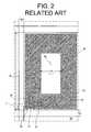
- FIG. 2is a schematic plan view showing one pixel region for a transflective LCD device having an uneven reflective layer according to the related art.
- a gate line 34is formed on a substrate 30 along a first direction, and a data line 46 crosses the gate line 34 to define a pixel region P.
- a thin film transistor Tis formed near a crossing of the gate line 34 and the data line 46 .
- a gate electrode 32 , a semiconductor layer 41 , source and drain electrodes 42 and 44constitute the thin film transistor T.
- a pixel electrode 60 of a transparent conductive materialis formed in the pixel region P and is connected to the thin film transistor T.
- a reflective layer 64 having a plurality of unevenesses 52is formed in the pixel region P and has a transmissive hole 58 that exposes the central portion of the pixel electrode 60 .
- the pixel region Pincludes a transmissive portion TP in the transmissive hole 58 and a reflective portion RP in a portion of the reflective layer 21 except a portion of the transmissive hole 58 .
- the pixel electrode 60acts as a driving electrode of the liquid crystal layer 18 (of FIG. 1 ) with the common electrode 13 (of FIG. 1 ).
- the reflective layer 64(or reflective electrode) mainly acts as a reflective means. Therefore, the uneven patterns increase reflectance of a surface of the reflective layer.
- FIGS. 3A to 3 Gare schematic cross sectional views taken along lines III-III of FIG. 2 , which shows a fabricating process for a transflective LCD device according to the related art.
- a switching region S, a transmissive portion TP, and a reflective portion RP in periphery of the transmissive portion TPare defined in a substrate 30 .
- the transmissive and reflective portion TP and RPconstitute a pixel region P.
- a gate electrode 32is formed on the substrate 30 in the switching region S.
- the gate electrode 32is formed as a single layer or a double layer.
- the gate electrode 32is selected from one of aluminum (Al), Al alloy, tungsten (W), chromium (Cr) and molybdenum (Mo).
- the gate electrode 32is selected from one of Al/Cr and Al/Mo.
- a gate insulating layer 36is formed of inorganic insulating materials over an entire surface of the substrate 30 having the gate electrode 32 , and an active layer 38 and an ohmic contact layer 40 are sequentially formed on the gate insulating layer 36 .
- the active layer 38 and the ohmic contact layer 40are made of intrinsic amorphous silicon and the doped amorphous silicon, respectively.
- the active layer 38 and the ohmic contact layer 40constitute a semiconductor layer 41 .
- source and drain electrodes 42 and 44are formed of a metallic material on the semiconductor layer 41
- a passivation layer 46is formed of an insulating material on an entire surface of the substrate 30 having the source and drain electrodes 42 and 44 .
- the passivation layer 46is made of an inorganic insulating material including silicon nitride (SiNx) and silicon oxide (SiOx).
- a photosensitive layer 50is formed of a photosensitive material on the passivation layer 46 .
- the photosensitive materialis selected from an organic material such as acrylic resin.
- This stepincludes forming an uneven pattern of squares (not shown) in a surface portion of the photosensitive layer 50 and forming the first uneven pattern 51 as a hemispherical shape by melting at a predetermined temperature within about 350 degrees Celsius.
- an inorganic insulating layer 54is formed of a transparent inorganic material on an entire surface of the substrate 30 having the first uneven pattern 51 of the hemispherical shape.
- the inorganic insulating layer 54has a second uneven pattern 52 of a hemispherical shape corresponding to the first uneven pattern 51 of the photosensitive layer 50 .
- the first and second uneven patterns 51 and 52are located in the reflective portion RP.
- portions of the passivation layer 46 , the photosensitive layer 50 and the inorganic insulating layer 54 that correspond to a portion of the drain electrode 44 and the transmissive portion TPare etched to form a drain contact hole 56 and a transmissive hole 58 that expose the portions of the drain electrode 44 and the transmissive portion TP, respectively.
- a portion of the gate insulating layer 36 in the transmissive hole 58may be etched due to etching rate differences between a portion of the drain contact hole 56 and a portion of the transmissive hole 58 as shown in FIG. 3E .
- a reflective layer 60is formed of metallic materials having a high reflectance such as aluminum (Al) and silver (Ag) on the substrate 30 having the drain contact hole 56 and the transmissive hole 58 .
- the reflective layer 60corresponds to the reflective portion RP except portions of the drain contact hole 56 and the transmissive hole 58 .
- an inorganic insulating layer 62is formed of an inorganic insulating material on the substrate 30 having the reflective layer 60 .
- the inorganic insulating layer 62has holes corresponding to the drain contact hole 56 and the transmissive hole 58 that can expose the portion of the drain electrode 42 and the transmissive portion TP.
- a pixel electrode 64is formed of transparent conductive materials such as indium tin oxide (ITO) on the inorganic insulating layer 62 and is connected to the drain electrode 44 via the drain contact hole 56 .
- ITOindium tin oxide
- the transflective LCD device according the related artis manufactured.
- a transflective liquid crystal display deviceincludes: a first substrate; a second substrate facing the first substrate; a liquid crystal layer interposed between the first and second substrates; a first polarizer on an outer side of the first substrate; a second polarizer on an outer side of the second substrate; an uneven transflective film on the first polarizer; and a backlight unit outside of the uneven transflective film.
- an uneven transflective filmin another aspect, includes: a base film including a plurality of convex patterns and a plurality of concave portions between the plurality of convex patterns; and a reflective layer in the plurality of concave portions.
- the reflective layeris formed on the concave patterns but not on the convex patterns.
- Each convex portionis defined from an apex of the curves in the base film (where the slope is zero) to a predetermined distance from the apex (where the slope is a set value).
- Each concave portionis defined from the predetermined distance from the apex to the point where the curve meets the adjacent curve or the curve otherwise terminates.
- the area of the convex portion bounded by the predetermined distancedefines the open area in which light is transmitted through the film.
- a method of fabricating an uneven transflective filmincludes: forming a plurality of convex patterns on a base film; forming a reflective material layer on an entire surface of the convex patterns; and etching the reflective material layer corresponding to the convex patterns to form a reflective layer between the convex patterns.
- FIG. 1is an exploded perspective view of an LCD device according to the related art.
- FIG. 2is a schematic plan view showing one pixel region for a transflective LCD device having an uneven reflective layer according to the related art.
- FIGS. 3A to 3 Gare schematic cross sectional views taken along lines III-III of FIG. 2 , which shows a fabricating process for a transflective LCD device according to the related art.
- FIG. 4is a schematic plan view showing one pixel region for a transflective LCD device having the uneven reflective layer according to the present invention.
- FIG. 5is a schematic plan view of an uneven transflective film according to the present invention.
- FIGS. 6A to 6 Eare schematic cross sectional views of a fabricating process for the uneven transflective film according to the present invention.
- FIG. 7is a schematic plan view of a reflective layer of an uneven transflective film according to the present invention.
- FIG. 4is a schematic plan view showing a transflective LCD device having an uneven transflective film according to one embodiment of the present invention.
- an LCD device 100includes a first substrate 200 , a second substrate 300 facing the first substrate 200 , a liquid crystal layer 400 interposed between the first and second substrates 200 and 300 , a first polarizer PL 1 on an outer side of the first substrate 200 , a second polarizer PL 2 on an outer side of the second substrate 300 .
- a pixel region Pis defined in each of the first and second substrates 200 and 300 .
- a gate electrode 202is formed on the first substrate 200 , a semiconductor layer 206 over the gate electrode 202 , and source and drain electrodes 208 and 210 on the semiconductor layer 206 .
- the gate electrode 202 , the semiconductor layer 206 , and the source and drain electrodes 208 and 210constitute a thin film transistor T.
- a pixel electrode 214is formed in the pixel region P of the first substrate 200 and is connected to the thin film transistor T.
- a black matrix 302is formed on the second substrate 300 , a color filter layer 304 on the black matrix 302 .
- the color filter layer 304includes a red sub-color filter 304 a , a green sub-color filter 304 b and a blue sub-color filter (not shown).
- Each of the red sub-color filter 304 a , the green sub-color filter 304 b and the blue sub-color filter (not shown)is located in the pixel region P.
- a common electrode 306is formed on an entire surface of the color filter layer 304 .
- a liquid crystal layer 400is interposed between the pixel electrode 214 and the common electrode 306 .
- the black matrix 302corresponds to a portion of the thin film transistor T and a portion that a gate line and a data line.
- an uneven transflective film 500is disposed on the first polarizer PL 1 , and a backlight unit BL is disposed outside of the uneven transflective film 500 .
- the uneven transflective film 500includes a plurality of convex patterns 502 having hemispherical shapes that face toward an inner side of the liquid crystal device 100 and a reflective layer 504 between the convex patterns 502 .
- a portion of the reflective layer 504corresponds to a reflection region where a first incident light L 1 from natural ambient light is reflected, and a portion of the convex patterns 502 corresponds to a transmission region where a second incident light L 2 from the backlight unit BL is transmitted.
- the LCD devicecan be both driven a reflective mode and a transmissive mode by the uneven transflective film without a reflective pattern such as the reflective layer 60 (of FIG. 3F ) inner side of the LCD device.
- the transflective LCD deviceaccording to one embodiment of the present invention can obtain high reflection efficiency and a wide-angle property.
- the uneven transflective film 500 and the first polarizer PL 1may be unified as a single body.
- FIG. 5is a schematic plan view of an uneven transflective film according to one embodiment of the present invention.
- an uneven transflective film 600includes a base film 602 including a plurality of convex patterns 604 and a plurality of concave portions CP between the plurality of convex patterns 604 , and a reflective layer 606 in the plurality of concave portions CP.
- a passivation layer 608 on the convex patterns 604 and the reflective layer 606is also included.
- the base film 602 and the passivation layer 608are selected from transparent materials. Specifically, the base film 602 is selected from a polymer based material such as polyester.
- the reflective layer 606is selected from a metallic material having a high reflectance such as aluminum (Al) and silver (Ag).
- the convex pattern 604has a hemispherical shape to improve reflection efficiency.
- the reflective layer 606may be formed as a single layer having open portions OP that correspond to the convex patterns 604 .
- a portion of the convex pattern 604is exposed through the open portion OP of the reflective layer 606 . Therefore, a portion of the reflective layer 606 between the convex patterns 604 is defined by a reflection region RR where incident light from in the top portion is reflected, a portion of the convex pattern 604 corresponding to the open portion OP is defined by a transmission region TR where incident light from outside in a back side of the convex pattern 604 is transmitted.
- the reflection efficiencyincreases, interference is prevented, and the viewing angle is improved by using the uneven transflective film 600 having the convex patterns 604 and the reflective layer 606 .
- FIGS. 6A to 6 Ea method of fabricating the uneven transflective film according to the present invention will be explained referring to FIGS. 6A to 6 E.
- a base film 602 that is selected from a polymer based material such as polyesteris prepared.
- a plurality of convex patterns 604are formed by stamping the top surface of the base film 602 .
- Each convex pattern 604has a hemispherical shape.
- the transflective LCD device having the uneven transflective film 600is manufactured simpler process than the transflective LCD device of the related art by omitting photolithography and melting of the reflective layer 64 (of FIG. 2 ) having the uneven patterns 52 (of FIG. 2 ).
- a reflective material layer 605is formed on an entire surface of the convex patterns 604 .
- the reflective material layer 605is selected from a metallic material having a high reflectance such as aluminum (Al) and silver (Ag).
- the reflective material layer 605 (of FIG. 6C ) corresponding to the convex patterns 604is removed by etching to form a reflective layer 606 between the convex patterns 604 .
- etching of the reflective material layer 605 (of FIG. 6C )is performed using photolithography.
- a passivation layer 608is formed on an entire surface of the convex patterns 604 and the reflective layer 606 .
- the base film 602 having the convex patterns 604 , the reflective layer 606 , and the passivation layer 608constitute an uneven transflective film 600 .
- the reflective layer 606is formed as a single body and has open portions OP corresponding to the convex patterns 604 .
- the open portions OPhave hexagonal shapes.
- the open portions OPcan have other shapes in combination with or instead of the hexagonal shapes.
- this uneven transflective film 600can be easily applied to the LCD device and can effectively improve reflection efficiency.
- a transflective LCD devicehas following advantages.
- the transflective LCD devicecan be both utilized in transmissive and reflective modes by including an uneven transflective film. Therefore, the transflective LCD device can be manufactured through a simpler process than that of the related art. Moreover, defect probability in the process, process time, and process cost can be reduced, thereby improving process yield and market competitiveness of production.
Landscapes
- Physics & Mathematics (AREA)
- Nonlinear Science (AREA)
- Mathematical Physics (AREA)
- Chemical & Material Sciences (AREA)
- Crystallography & Structural Chemistry (AREA)
- General Physics & Mathematics (AREA)
- Optics & Photonics (AREA)
- Liquid Crystal (AREA)
- Optical Elements Other Than Lenses (AREA)
Abstract
Description
- This application claims the benefit of the Korean Patent Application No. 2003-99358, filed in Korea on Dec. 29, 2003, which is hereby incorporated by reference for all purposes as it fully set forth herein.
- 1. Field
- The present invention relates to a liquid crystal display device, and more particularly, to a transflective liquid crystal display device having high utilization efficiency for light and a fabricating method thereof.
- 2. Discussion of the Related Art
- Generally, transflective liquid crystal display (LCD) devices function as both transmissive and reflective LCD devices. Because transflective LCD devices can use both a backlight and natural or artificial ambient light, the transflective LCD devices may be used in more circumstances, and power consumption of transflective LCD devices may be reduced.
FIG. 1 is an exploded perspective view of an LCD device according to the related art. As shown inFIG. 1 , a liquid crystal display (LCD)device 10 has anupper substrate 12 having ablack matrix 17, acolor filter layer 16 including sub-color filters and acommon electrode 13 on thecolor filter layer 16, and alower substrate 14 having a thin film transistor (TFT) T and apixel electrode 20 connected to the TFT T. Aliquid crystal layer 18 is interposed between thecommon electrode 13 and thepixel electrode 20. Thelower substrate 14 is referred to as an array substrate because array lines including agate line 25 and adata line 27 are formed thereon. Thegate line 25 and thedata line 27 cross each other forming a matrix, and the TFT T is connected to thegate line 25 and thedata line 27. Thegate line 25 and thedata line 27 define a pixel region P by crossing each other, and the TFT T is formed near a crossing portion of thegate line 25 and thedata line 27. Thepixel electrode 20 is formed of a transparent conductive material such as indium-tin-oxide (ITO) and indium-zinc-oxide (IZO) in the pixel region P. Theupper substrate 12 is referred to as a color filter substrate because thecolor filter layer 16 is formed thereon.- A
reflective layer 21 of a reflective material such as aluminum (Al) or Al alloy is formed in the pixel region P. However, when thereflective layer 21 is connected to thepixel electrode 20, thereflective layer 21 can act as an electrode. Thereflective layer 21 has a transmittance hole H so that the pixel region P is divided into a reflective portion RP and a transmissive portion TP. The transmissive portion TP corresponds to the transmissive hole H and the reflective portion RP corresponds to the other portions of thereflective layer 21. - However, because the transflective LCD device is manufactured to selectively use a reflective mode or a transmissive mode, utilization efficiency for light is relatively low. Particularly, when the transflective LCD device is used as the reflective mode, it depends on natural light. Therefore, the utilization efficiency is low in comparison with the transmissive mode. As a result, interchanging the reflective mode with the transmissive mode causes a brightness difference.
- To solve these problems, an uneven reflective layer is formed on the reflective portion to induce an irregular reflection by minimizing incident light specularly-reflected from outside and to improve the entire brightness of the reflective mode and transmissive mode according to the related art.
- Hereinafter, the transflective LCD device having the uneven reflective layer according to the related art will be explained referring to
FIG. 2 . FIG. 2 is a schematic plan view showing one pixel region for a transflective LCD device having an uneven reflective layer according to the related art.- In
FIG. 2 , a gate line34 is formed on asubstrate 30 along a first direction, and adata line 46 crosses the gate line34 to define a pixel region P. - A thin film transistor T is formed near a crossing of the gate line34 and the
data line 46. Agate electrode 32, asemiconductor layer 41, source anddrain electrodes - A
pixel electrode 60 of a transparent conductive material is formed in the pixel region P and is connected to the thin film transistor T. Areflective layer 64 having a plurality ofunevenesses 52 is formed in the pixel region P and has atransmissive hole 58 that exposes the central portion of thepixel electrode 60. - The pixel region P includes a transmissive portion TP in the
transmissive hole 58 and a reflective portion RP in a portion of thereflective layer 21 except a portion of thetransmissive hole 58. - That is to say, the
pixel electrode 60 acts as a driving electrode of the liquid crystal layer18 (ofFIG. 1 ) with the common electrode13 (ofFIG. 1 ). On the other hand, the reflective layer64 (or reflective electrode) mainly acts as a reflective means. Therefore, the uneven patterns increase reflectance of a surface of the reflective layer. - Next, it will be explained about the fabricating method for the transflective LCD device having the uneven reflective layer according to the related art.
FIGS. 3A to3G are schematic cross sectional views taken along lines III-III ofFIG. 2 , which shows a fabricating process for a transflective LCD device according to the related art.- In
FIG. 3A , a switching region S, a transmissive portion TP, and a reflective portion RP in periphery of the transmissive portion TP are defined in asubstrate 30. The transmissive and reflective portion TP and RP constitute a pixel region P. - A
gate electrode 32 is formed on thesubstrate 30 in the switching region S. For example, thegate electrode 32 is formed as a single layer or a double layer. When thegate electrode 32 is a single layer, it is selected from one of aluminum (Al), Al alloy, tungsten (W), chromium (Cr) and molybdenum (Mo). Meanwhile, when thegate electrode 32 is a double layer, thegate electrode 32 is selected from one of Al/Cr and Al/Mo. - In
FIG. 3B , agate insulating layer 36 is formed of inorganic insulating materials over an entire surface of thesubstrate 30 having thegate electrode 32, and anactive layer 38 and anohmic contact layer 40 are sequentially formed on thegate insulating layer 36. Theactive layer 38 and theohmic contact layer 40 are made of intrinsic amorphous silicon and the doped amorphous silicon, respectively. Theactive layer 38 and theohmic contact layer 40 constitute asemiconductor layer 41. - In
FIG. 3C , source anddrain electrodes semiconductor layer 41, and apassivation layer 46 is formed of an insulating material on an entire surface of thesubstrate 30 having the source anddrain electrodes semiconductor layer 41 and thepassivation layer 46, thepassivation layer 46 is made of an inorganic insulating material including silicon nitride (SiNx) and silicon oxide (SiOx). - In
FIG. 3D , aphotosensitive layer 50 is formed of a photosensitive material on thepassivation layer 46. The photosensitive material is selected from an organic material such as acrylic resin. This step includes forming an uneven pattern of squares (not shown) in a surface portion of thephotosensitive layer 50 and forming the firstuneven pattern 51 as a hemispherical shape by melting at a predetermined temperature within about 350 degrees Celsius. - Next, an
inorganic insulating layer 54 is formed of a transparent inorganic material on an entire surface of thesubstrate 30 having the firstuneven pattern 51 of the hemispherical shape. At this time, theinorganic insulating layer 54 has a seconduneven pattern 52 of a hemispherical shape corresponding to the firstuneven pattern 51 of thephotosensitive layer 50. The first and seconduneven patterns - In
FIG. 3E , portions of thepassivation layer 46, thephotosensitive layer 50 and the inorganicinsulating layer 54 that correspond to a portion of thedrain electrode 44 and the transmissive portion TP are etched to form adrain contact hole 56 and atransmissive hole 58 that expose the portions of thedrain electrode 44 and the transmissive portion TP, respectively. Specifically, a portion of thegate insulating layer 36 in thetransmissive hole 58 may be etched due to etching rate differences between a portion of thedrain contact hole 56 and a portion of thetransmissive hole 58 as shown inFIG. 3E . - In
FIG. 3F , areflective layer 60 is formed of metallic materials having a high reflectance such as aluminum (Al) and silver (Ag) on thesubstrate 30 having thedrain contact hole 56 and thetransmissive hole 58. Thereflective layer 60 corresponds to the reflective portion RP except portions of thedrain contact hole 56 and thetransmissive hole 58. - In
FIG. 3G , an inorganic insulatinglayer 62 is formed of an inorganic insulating material on thesubstrate 30 having thereflective layer 60. At this time, through this step, the inorganic insulatinglayer 62 has holes corresponding to thedrain contact hole 56 and thetransmissive hole 58 that can expose the portion of thedrain electrode 42 and the transmissive portion TP. - Next, a
pixel electrode 64 is formed of transparent conductive materials such as indium tin oxide (ITO) on the inorganic insulatinglayer 62 and is connected to thedrain electrode 44 via thedrain contact hole 56. - As explained above, the transflective LCD device according the related art is manufactured.
- However, this method of fabricating for the transflective LCD device according to the related art uses a large number of processes and thus the overall process becomes complicated. Therefore, production yield of the transflective LCD device is reduced.
- By way of introduction only, in one aspect, a transflective liquid crystal display device includes: a first substrate; a second substrate facing the first substrate; a liquid crystal layer interposed between the first and second substrates; a first polarizer on an outer side of the first substrate; a second polarizer on an outer side of the second substrate; an uneven transflective film on the first polarizer; and a backlight unit outside of the uneven transflective film.
- In another aspect, an uneven transflective film includes: a base film including a plurality of convex patterns and a plurality of concave portions between the plurality of convex patterns; and a reflective layer in the plurality of concave portions. The reflective layer is formed on the concave patterns but not on the convex patterns. Each convex portion is defined from an apex of the curves in the base film (where the slope is zero) to a predetermined distance from the apex (where the slope is a set value). Each concave portion is defined from the predetermined distance from the apex to the point where the curve meets the adjacent curve or the curve otherwise terminates. The area of the convex portion bounded by the predetermined distance defines the open area in which light is transmitted through the film.
- In another aspect, a method of fabricating an uneven transflective film includes: forming a plurality of convex patterns on a base film; forming a reflective material layer on an entire surface of the convex patterns; and etching the reflective material layer corresponding to the convex patterns to form a reflective layer between the convex patterns.
- It is to be understood that both the foregoing general description and the following detailed description of the present invention are exemplary and explanatory and are intended to provide further explanation of the invention as claimed.
- The accompanying drawings, which are included to provide a further understanding of the invention and are incorporated in and constitute a part of this application, illustrate embodiments of the invention and together with the description serve to explain the principles of the invention.
- In the drawings:
FIG. 1 is an exploded perspective view of an LCD device according to the related art.FIG. 2 is a schematic plan view showing one pixel region for a transflective LCD device having an uneven reflective layer according to the related art.FIGS. 3A to3G are schematic cross sectional views taken along lines III-III ofFIG. 2 , which shows a fabricating process for a transflective LCD device according to the related art.FIG. 4 is a schematic plan view showing one pixel region for a transflective LCD device having the uneven reflective layer according to the present invention.FIG. 5 is a schematic plan view of an uneven transflective film according to the present invention.FIGS. 6A to6E are schematic cross sectional views of a fabricating process for the uneven transflective film according to the present invention.FIG. 7 is a schematic plan view of a reflective layer of an uneven transflective film according to the present invention.- Reference will now be made in detail to the illustrated embodiments of the present invention, examples of which are illustrated in the accompanying drawings.
FIG. 4 is a schematic plan view showing a transflective LCD device having an uneven transflective film according to one embodiment of the present invention.- In
FIG. 4 , anLCD device 100 includes afirst substrate 200, asecond substrate 300 facing thefirst substrate 200, aliquid crystal layer 400 interposed between the first andsecond substrates first substrate 200, a second polarizer PL2 on an outer side of thesecond substrate 300. - At this time, a pixel region P is defined in each of the first and
second substrates gate electrode 202 is formed on thefirst substrate 200, asemiconductor layer 206 over thegate electrode 202, and source and drainelectrodes semiconductor layer 206. Thegate electrode 202, thesemiconductor layer 206, and the source and drainelectrodes pixel electrode 214 is formed in the pixel region P of thefirst substrate 200 and is connected to the thin film transistor T. - A
black matrix 302 is formed on thesecond substrate 300, acolor filter layer 304 on theblack matrix 302. Thecolor filter layer 304 includes a redsub-color filter 304a, a greensub-color filter 304band a blue sub-color filter (not shown). Each of the redsub-color filter 304a, the greensub-color filter 304band the blue sub-color filter (not shown) is located in the pixel region P. Acommon electrode 306 is formed on an entire surface of thecolor filter layer 304. In addition, aliquid crystal layer 400 is interposed between thepixel electrode 214 and thecommon electrode 306. - Although not shown, the
black matrix 302 corresponds to a portion of the thin film transistor T and a portion that a gate line and a data line. - In addition, an
uneven transflective film 500 is disposed on the first polarizer PL1, and a backlight unit BL is disposed outside of theuneven transflective film 500. At this time, theuneven transflective film 500 includes a plurality ofconvex patterns 502 having hemispherical shapes that face toward an inner side of theliquid crystal device 100 and areflective layer 504 between theconvex patterns 502. - Although not shown, a portion of the
reflective layer 504 corresponds to a reflection region where a first incident light L1 from natural ambient light is reflected, and a portion of theconvex patterns 502 corresponds to a transmission region where a second incident light L2 from the backlight unit BL is transmitted. - Therefore, the LCD device can be both driven a reflective mode and a transmissive mode by the uneven transflective film without a reflective pattern such as the reflective layer60 (of
FIG. 3F ) inner side of the LCD device. Specifically, because of the hemispherical shape of theconvex pattern 502, the transflective LCD device according to one embodiment of the present invention can obtain high reflection efficiency and a wide-angle property. Although not shown, theuneven transflective film 500 and the first polarizer PL1 may be unified as a single body. - Hereinafter, a specific structure of the
uneven transflective film 500 will be explained as referring toFIG. 5 . FIG. 5 is a schematic plan view of an uneven transflective film according to one embodiment of the present invention.- In
FIG. 5 , anuneven transflective film 600 includes abase film 602 including a plurality ofconvex patterns 604 and a plurality of concave portions CP between the plurality ofconvex patterns 604, and areflective layer 606 in the plurality of concave portions CP. In addition, apassivation layer 608 on theconvex patterns 604 and thereflective layer 606. - The
base film 602 and thepassivation layer 608 are selected from transparent materials. Specifically, thebase film 602 is selected from a polymer based material such as polyester. Thereflective layer 606 is selected from a metallic material having a high reflectance such as aluminum (Al) and silver (Ag). - Specifically, the
convex pattern 604 has a hemispherical shape to improve reflection efficiency. Although not shown, thereflective layer 606 may be formed as a single layer having open portions OP that correspond to theconvex patterns 604. In other words, a portion of theconvex pattern 604 is exposed through the open portion OP of thereflective layer 606. Therefore, a portion of thereflective layer 606 between theconvex patterns 604 is defined by a reflection region RR where incident light from in the top portion is reflected, a portion of theconvex pattern 604 corresponding to the open portion OP is defined by a transmission region TR where incident light from outside in a back side of theconvex pattern 604 is transmitted. - Accordingly, the reflection efficiency increases, interference is prevented, and the viewing angle is improved by using the
uneven transflective film 600 having theconvex patterns 604 and thereflective layer 606. - Hereinafter, a method of fabricating the uneven transflective film according to the present invention will be explained referring to
FIGS. 6A to6E. - In
FIG. 6A , abase film 602 that is selected from a polymer based material such as polyester is prepared. - Next, in
FIG. 6B , a plurality ofconvex patterns 604 are formed by stamping the top surface of thebase film 602. Eachconvex pattern 604 has a hemispherical shape. - That is to say, the transflective LCD device having the
uneven transflective film 600 is manufactured simpler process than the transflective LCD device of the related art by omitting photolithography and melting of the reflective layer64 (ofFIG. 2 ) having the uneven patterns52 (ofFIG. 2 ). - In
FIG. 6C , areflective material layer 605 is formed on an entire surface of theconvex patterns 604. Thereflective material layer 605 is selected from a metallic material having a high reflectance such as aluminum (Al) and silver (Ag). - In
FIG. 6D , the reflective material layer605 (ofFIG. 6C ) corresponding to theconvex patterns 604 is removed by etching to form areflective layer 606 between theconvex patterns 604. For example, etching of the reflective material layer605 (ofFIG. 6C ) is performed using photolithography. - In
FIG. 6E , apassivation layer 608 is formed on an entire surface of theconvex patterns 604 and thereflective layer 606. - The
base film 602 having theconvex patterns 604, thereflective layer 606, and thepassivation layer 608 constitute anuneven transflective film 600. - Hereinafter, a plan structure of the reflective layer of the
uneven transflective film 600 according to the present invention will be explained as referring toFIG. 7 . - As shown in
FIG. 7 , thereflective layer 606 is formed as a single body and has open portions OP corresponding to theconvex patterns 604. For example, the open portions OP have hexagonal shapes. However, the open portions OP can have other shapes in combination with or instead of the hexagonal shapes. - As explained above, this
uneven transflective film 600 can be easily applied to the LCD device and can effectively improve reflection efficiency. - Consequently, a transflective LCD device according to embodiments of the present invention has following advantages. First, the transflective LCD device can be both utilized in transmissive and reflective modes by including an uneven transflective film. Therefore, the transflective LCD device can be manufactured through a simpler process than that of the related art. Moreover, defect probability in the process, process time, and process cost can be reduced, thereby improving process yield and market competitiveness of production. Second, reflection and transmission efficiency can be increased. Third, because of the hemispherical shape of the uneven transflective film, the brightness of the display can be viewed in a wider angular range.
- It will be apparent to those skilled in the art that various modifications and variations can be made in a transflective LCD device and a fabricating method thereof of the present invention without departing from the spirit or scope of the invention. Thus, it is intended that the present invention cover the modifications and variations of this invention provided they come within the scope of the appended claims and their equivalents.
Claims (34)
Applications Claiming Priority (2)
| Application Number | Priority Date | Filing Date | Title |
|---|---|---|---|
| KR1020030099358AKR101005355B1 (en) | 2003-12-29 | 2003-12-29 | Reflective liquid crystal display device and manufacturing method |
| KRP2003-99358 | 2003-12-29 |
Publications (2)
| Publication Number | Publication Date |
|---|---|
| US20050140879A1true US20050140879A1 (en) | 2005-06-30 |
| US7545465B2 US7545465B2 (en) | 2009-06-09 |
Family
ID=34698694
Family Applications (1)
| Application Number | Title | Priority Date | Filing Date |
|---|---|---|---|
| US11/025,219Expired - Fee RelatedUS7545465B2 (en) | 2003-12-29 | 2004-12-28 | Transflective liquid crystal display device and fabricating method thereof |
Country Status (3)
| Country | Link |
|---|---|
| US (1) | US7545465B2 (en) |
| KR (1) | KR101005355B1 (en) |
| CN (1) | CN100356244C (en) |
Cited By (7)
| Publication number | Priority date | Publication date | Assignee | Title |
|---|---|---|---|---|
| US20070279559A1 (en)* | 2006-06-02 | 2007-12-06 | Nec Lcd Technologies, Ltd. | Transflective liquid crystal display apparatus |
| US20110157887A1 (en)* | 2009-12-24 | 2011-06-30 | Samsung Mobile Display Co., Ltd. | Optical film and organic light emitting dislay apparatus comprising the same |
| US20110176304A1 (en)* | 2010-01-19 | 2011-07-21 | Samsung Mobile Display Co., Ltd. | Optical Film and Organic Light Emitting Display Apparatus Including the Same |
| US8979342B2 (en) | 2011-08-19 | 2015-03-17 | Barnesandnoble.Com Llc | Planar front illumination system having a light guide with micro scattering features formed thereon and method of manufacturing the same |
| JP2015079277A (en)* | 2009-12-28 | 2015-04-23 | 株式会社半導体エネルギー研究所 | Electronic apparatus |
| US9285530B2 (en) | 2011-08-19 | 2016-03-15 | Nook Digital, Llc | Planar front illumination system having a light guide with micro lenses formed thereon and method of manufacturing the same |
| US9385170B2 (en)* | 2012-11-06 | 2016-07-05 | Samsung Display Co., Ltd. | Thin film transistor array panel and organic light emitting diode display including the same |
Families Citing this family (6)
| Publication number | Priority date | Publication date | Assignee | Title |
|---|---|---|---|---|
| CN100405169C (en)* | 2006-09-21 | 2008-07-23 | 友达光电股份有限公司 | Semi-penetration reflection type display |
| FI20070991L (en)* | 2007-12-19 | 2009-06-20 | Beneq Oy | Glass product, product use and manufacturing method |
| KR101665062B1 (en)* | 2009-12-08 | 2016-10-24 | 엘지디스플레이 주식회사 | An array substrate for trans-flective liquid crystal display device and method of fabricating the same |
| CN106898615B (en)* | 2017-02-28 | 2020-06-30 | 京东方科技集团股份有限公司 | Reflection-type array substrate, preparation method thereof and display device |
| CN112558347A (en)* | 2020-12-04 | 2021-03-26 | 惠州Tcl移动通信有限公司 | Reflective liquid crystal display panel and display device |
| CN115718387B (en)* | 2022-11-28 | 2023-11-07 | 京东方科技集团股份有限公司 | Reflection type array substrate and manufacturing method thereof, display device and manufacturing method thereof |
Citations (9)
| Publication number | Priority date | Publication date | Assignee | Title |
|---|---|---|---|---|
| US6124971A (en)* | 1995-06-26 | 2000-09-26 | 3M Innovative Properties Company | Transflective displays with reflective polarizing transflector |
| US6285426B1 (en)* | 1998-07-06 | 2001-09-04 | Motorola, Inc. | Ridged reflector having optically transmissive properties for an optical display device |
| US20030038907A1 (en)* | 2001-08-22 | 2003-02-27 | Nec Corporation | Liquid crystal display |
| US6538711B2 (en)* | 1998-07-31 | 2003-03-25 | Hitachi, Ltd. | Method of manufacturing reflective liquid crystal display device |
| US20030090607A1 (en)* | 2001-10-24 | 2003-05-15 | Seiko Epson Corporation | Liquid crystal display device and electronic apparatus |
| US20040021810A1 (en)* | 2000-07-28 | 2004-02-05 | Mariko Kawaguri | Reflection sheet and production method therefor and display unit using it |
| US20040056997A1 (en)* | 2000-07-03 | 2004-03-25 | Katsumasa Yoshii | Reflector providing particularly high reflectance in an intended viewing angle and reflection type liquid crystal display device using the same |
| US6750932B2 (en)* | 2001-10-12 | 2004-06-15 | Lg.Philips Lcd Co., Ltd. | Transflective liquid crystal display device, method of fabricating the same, and method of using the same |
| US6924858B2 (en)* | 2001-07-06 | 2005-08-02 | Kabushiki Kaisha Toshiba | Liquid crystal display unit |
Family Cites Families (4)
| Publication number | Priority date | Publication date | Assignee | Title |
|---|---|---|---|---|
| JP2001075091A (en)* | 1999-07-07 | 2001-03-23 | Matsushita Electric Ind Co Ltd | Transflective liquid crystal display |
| JP2001235606A (en)* | 1999-12-13 | 2001-08-31 | Sumitomo Chem Co Ltd | Optical member having reflection function and transmission function |
| JP3598987B2 (en)* | 2001-03-28 | 2004-12-08 | セイコーエプソン株式会社 | Liquid crystal display and electronic equipment |
| JP4546730B2 (en) | 2001-12-18 | 2010-09-15 | サムスン エレクトロニクス カンパニー リミテッド | Transflective liquid crystal display device |
- 2003
- 2003-12-29KRKR1020030099358Apatent/KR101005355B1/ennot_activeExpired - Fee Related
- 2004
- 2004-12-28USUS11/025,219patent/US7545465B2/ennot_activeExpired - Fee Related
- 2004-12-29CNCNB2004101029889Apatent/CN100356244C/ennot_activeExpired - Fee Related
Patent Citations (10)
| Publication number | Priority date | Publication date | Assignee | Title |
|---|---|---|---|---|
| US6124971A (en)* | 1995-06-26 | 2000-09-26 | 3M Innovative Properties Company | Transflective displays with reflective polarizing transflector |
| US6262842B1 (en)* | 1995-06-26 | 2001-07-17 | 3M Innovative Properties Company | Transflective displays with reflective polarizing transflector |
| US6285426B1 (en)* | 1998-07-06 | 2001-09-04 | Motorola, Inc. | Ridged reflector having optically transmissive properties for an optical display device |
| US6538711B2 (en)* | 1998-07-31 | 2003-03-25 | Hitachi, Ltd. | Method of manufacturing reflective liquid crystal display device |
| US20040056997A1 (en)* | 2000-07-03 | 2004-03-25 | Katsumasa Yoshii | Reflector providing particularly high reflectance in an intended viewing angle and reflection type liquid crystal display device using the same |
| US20040021810A1 (en)* | 2000-07-28 | 2004-02-05 | Mariko Kawaguri | Reflection sheet and production method therefor and display unit using it |
| US6924858B2 (en)* | 2001-07-06 | 2005-08-02 | Kabushiki Kaisha Toshiba | Liquid crystal display unit |
| US20030038907A1 (en)* | 2001-08-22 | 2003-02-27 | Nec Corporation | Liquid crystal display |
| US6750932B2 (en)* | 2001-10-12 | 2004-06-15 | Lg.Philips Lcd Co., Ltd. | Transflective liquid crystal display device, method of fabricating the same, and method of using the same |
| US20030090607A1 (en)* | 2001-10-24 | 2003-05-15 | Seiko Epson Corporation | Liquid crystal display device and electronic apparatus |
Cited By (13)
| Publication number | Priority date | Publication date | Assignee | Title |
|---|---|---|---|---|
| US7679700B2 (en)* | 2006-06-02 | 2010-03-16 | Nec Lcd Technologies, Ltd. | Transflective liquid crystal display apparatus |
| US20100123863A1 (en)* | 2006-06-02 | 2010-05-20 | Nec Lcd Technologies, Ltd. | Transflective liquid crystal display apparatus |
| US7924377B2 (en) | 2006-06-02 | 2011-04-12 | Nec Lcd Technologies, Ltd. | Transflective liquid crystal display apparatus |
| US20070279559A1 (en)* | 2006-06-02 | 2007-12-06 | Nec Lcd Technologies, Ltd. | Transflective liquid crystal display apparatus |
| US8998446B2 (en) | 2009-12-24 | 2015-04-07 | Samsung Display Co., Ltd. | Optical film and organic light emitting display apparatus comprising the same |
| US20110157887A1 (en)* | 2009-12-24 | 2011-06-30 | Samsung Mobile Display Co., Ltd. | Optical film and organic light emitting dislay apparatus comprising the same |
| JP2015079277A (en)* | 2009-12-28 | 2015-04-23 | 株式会社半導体エネルギー研究所 | Electronic apparatus |
| JP2017227939A (en)* | 2009-12-28 | 2017-12-28 | 株式会社半導体エネルギー研究所 | Liquid crystal display device |
| US8550667B2 (en) | 2010-01-19 | 2013-10-08 | Samsung Display Co., Ltd. | Optical film and organic light emitting display apparatus including the same |
| US20110176304A1 (en)* | 2010-01-19 | 2011-07-21 | Samsung Mobile Display Co., Ltd. | Optical Film and Organic Light Emitting Display Apparatus Including the Same |
| US8979342B2 (en) | 2011-08-19 | 2015-03-17 | Barnesandnoble.Com Llc | Planar front illumination system having a light guide with micro scattering features formed thereon and method of manufacturing the same |
| US9285530B2 (en) | 2011-08-19 | 2016-03-15 | Nook Digital, Llc | Planar front illumination system having a light guide with micro lenses formed thereon and method of manufacturing the same |
| US9385170B2 (en)* | 2012-11-06 | 2016-07-05 | Samsung Display Co., Ltd. | Thin film transistor array panel and organic light emitting diode display including the same |
Also Published As
| Publication number | Publication date |
|---|---|
| KR101005355B1 (en) | 2011-01-05 |
| CN1637517A (en) | 2005-07-13 |
| US7545465B2 (en) | 2009-06-09 |
| KR20050068194A (en) | 2005-07-05 |
| CN100356244C (en) | 2007-12-19 |
Similar Documents
| Publication | Publication Date | Title |
|---|---|---|
| US7440055B2 (en) | Transflective liquid crystal display device and fabricating method thereof | |
| US7567329B2 (en) | Liquid crystal display device and method of fabricating the same | |
| US7502093B2 (en) | Method for fabricating a transflective liquid crystal display device | |
| US8054424B2 (en) | Transflective liquid crystal display device and manufacturing method thereof | |
| US7667800B2 (en) | Liquid crystal display device and method of fabricating the same | |
| US20040124414A1 (en) | Transflective liquid crystal display device and fabricating method thereof | |
| US6888597B2 (en) | Method of array substrate for transflective liquid crystal display device | |
| US7545465B2 (en) | Transflective liquid crystal display device and fabricating method thereof | |
| US8576361B2 (en) | Transreflective liquid crystal display device and fabricating method thereof having uneven patterns consisting of organic material in the reflective portion | |
| KR100475110B1 (en) | Reflective type Liquid Crystal Display Device and method for manufacturing the same | |
| CN113625485A (en) | Array substrate, manufacturing method thereof and display device | |
| KR20050068852A (en) | A substrate for transflective lcd and method for fabricating of the same | |
| CN1988163A (en) | Array substrate, method of manufacturing the same and display panel having the same | |
| US20070188682A1 (en) | Method for manufacturing a display device | |
| US20040125288A1 (en) | Method of fabricating liquid crystal display device having concave reflector | |
| JP2004144965A (en) | Semitransmissive liquid crystal display | |
| US7791693B2 (en) | Semi-transmission liquid crystal display device and fabricating method thereof | |
| KR20070072299A (en) | LCD and its manufacturing method | |
| KR20050060568A (en) | Transflective lcd | |
| KR100961697B1 (en) | Manufacturing Method of Array Board for Reflective Liquid Crystal Display | |
| KR20060017964A (en) | Transflective type liquid crystal display device and transflective type liquid crystal display device | |
| KR20060001131A (en) | Reflective type liquid crystal display device and transflective film provided therein | |
| KR20060079705A (en) | Liquid Crystal Display, Internal Polarizer and Formation Method | |
| KR20070069836A (en) | Semi-transmissive liquid crystal display device and manufacturing method thereof |
Legal Events
| Date | Code | Title | Description |
|---|---|---|---|
| AS | Assignment | Owner name:LG.PHILIPS LCD CO., LTD., KOREA, REPUBLIC OF Free format text:ASSIGNMENT OF ASSIGNORS INTEREST;ASSIGNOR:NAM, CHUL;REEL/FRAME:016141/0976 Effective date:20041223 | |
| AS | Assignment | Owner name:LG DISPLAY CO. LTD., KOREA, REPUBLIC OF Free format text:CHANGE OF NAME;ASSIGNOR:LG. PHILIPS LCD CO., LTD.;REEL/FRAME:020976/0243 Effective date:20080229 Owner name:LG DISPLAY CO. LTD.,KOREA, REPUBLIC OF Free format text:CHANGE OF NAME;ASSIGNOR:LG. PHILIPS LCD CO., LTD.;REEL/FRAME:020976/0243 Effective date:20080229 | |
| FEPP | Fee payment procedure | Free format text:PAYOR NUMBER ASSIGNED (ORIGINAL EVENT CODE: ASPN); ENTITY STATUS OF PATENT OWNER: LARGE ENTITY | |
| STCF | Information on status: patent grant | Free format text:PATENTED CASE | |
| FEPP | Fee payment procedure | Free format text:PAYER NUMBER DE-ASSIGNED (ORIGINAL EVENT CODE: RMPN); ENTITY STATUS OF PATENT OWNER: LARGE ENTITY Free format text:PAYOR NUMBER ASSIGNED (ORIGINAL EVENT CODE: ASPN); ENTITY STATUS OF PATENT OWNER: LARGE ENTITY | |
| FPAY | Fee payment | Year of fee payment:4 | |
| FPAY | Fee payment | Year of fee payment:8 | |
| LAPS | Lapse for failure to pay maintenance fees | Free format text:PATENT EXPIRED FOR FAILURE TO PAY MAINTENANCE FEES (ORIGINAL EVENT CODE: EXP.); ENTITY STATUS OF PATENT OWNER: LARGE ENTITY | |
| FEPP | Fee payment procedure | Free format text:MAINTENANCE FEE REMINDER MAILED (ORIGINAL EVENT CODE: REM.); ENTITY STATUS OF PATENT OWNER: LARGE ENTITY | |
| STCH | Information on status: patent discontinuation | Free format text:PATENT EXPIRED DUE TO NONPAYMENT OF MAINTENANCE FEES UNDER 37 CFR 1.362 | |
| FP | Lapsed due to failure to pay maintenance fee | Effective date:20210609 |