US20050139980A1 - High density integrated circuit module - Google Patents
High density integrated circuit moduleDownload PDFInfo
- Publication number
- US20050139980A1 US20050139980A1US11/040,564US4056405AUS2005139980A1US 20050139980 A1US20050139980 A1US 20050139980A1US 4056405 AUS4056405 AUS 4056405AUS 2005139980 A1US2005139980 A1US 2005139980A1
- Authority
- US
- United States
- Prior art keywords
- package
- bga package
- lead
- bga
- contacts
- Prior art date
- Legal status (The legal status is an assumption and is not a legal conclusion. Google has not performed a legal analysis and makes no representation as to the accuracy of the status listed.)
- Abandoned
Links
Images

Classifications
- H—ELECTRICITY
- H01—ELECTRIC ELEMENTS
- H01L—SEMICONDUCTOR DEVICES NOT COVERED BY CLASS H10
- H01L23/00—Details of semiconductor or other solid state devices
- H01L23/48—Arrangements for conducting electric current to or from the solid state body in operation, e.g. leads, terminal arrangements ; Selection of materials therefor
- H01L23/488—Arrangements for conducting electric current to or from the solid state body in operation, e.g. leads, terminal arrangements ; Selection of materials therefor consisting of soldered or bonded constructions
- H01L23/495—Lead-frames or other flat leads
- H01L23/49537—Plurality of lead frames mounted in one device
- H—ELECTRICITY
- H01—ELECTRIC ELEMENTS
- H01L—SEMICONDUCTOR DEVICES NOT COVERED BY CLASS H10
- H01L23/00—Details of semiconductor or other solid state devices
- H01L23/48—Arrangements for conducting electric current to or from the solid state body in operation, e.g. leads, terminal arrangements ; Selection of materials therefor
- H01L23/488—Arrangements for conducting electric current to or from the solid state body in operation, e.g. leads, terminal arrangements ; Selection of materials therefor consisting of soldered or bonded constructions
- H01L23/495—Lead-frames or other flat leads
- H01L23/49503—Lead-frames or other flat leads characterised by the die pad
- H01L23/4951—Chip-on-leads or leads-on-chip techniques, i.e. inner lead fingers being used as die pad
- H—ELECTRICITY
- H01—ELECTRIC ELEMENTS
- H01L—SEMICONDUCTOR DEVICES NOT COVERED BY CLASS H10
- H01L23/00—Details of semiconductor or other solid state devices
- H01L23/48—Arrangements for conducting electric current to or from the solid state body in operation, e.g. leads, terminal arrangements ; Selection of materials therefor
- H01L23/488—Arrangements for conducting electric current to or from the solid state body in operation, e.g. leads, terminal arrangements ; Selection of materials therefor consisting of soldered or bonded constructions
- H01L23/495—Lead-frames or other flat leads
- H01L23/49541—Geometry of the lead-frame
- H—ELECTRICITY
- H01—ELECTRIC ELEMENTS
- H01L—SEMICONDUCTOR DEVICES NOT COVERED BY CLASS H10
- H01L25/00—Assemblies consisting of a plurality of semiconductor or other solid state devices
- H01L25/03—Assemblies consisting of a plurality of semiconductor or other solid state devices all the devices being of a type provided for in a single subclass of subclasses H10B, H10D, H10F, H10H, H10K or H10N, e.g. assemblies of rectifier diodes
- H01L25/10—Assemblies consisting of a plurality of semiconductor or other solid state devices all the devices being of a type provided for in a single subclass of subclasses H10B, H10D, H10F, H10H, H10K or H10N, e.g. assemblies of rectifier diodes the devices having separate containers
- H01L25/105—Assemblies consisting of a plurality of semiconductor or other solid state devices all the devices being of a type provided for in a single subclass of subclasses H10B, H10D, H10F, H10H, H10K or H10N, e.g. assemblies of rectifier diodes the devices having separate containers the devices being integrated devices of class H10
- H—ELECTRICITY
- H01—ELECTRIC ELEMENTS
- H01L—SEMICONDUCTOR DEVICES NOT COVERED BY CLASS H10
- H01L2225/00—Details relating to assemblies covered by the group H01L25/00 but not provided for in its subgroups
- H01L2225/03—All the devices being of a type provided for in the same main group of the same subclass of class H10, e.g. assemblies of rectifier diodes
- H01L2225/10—All the devices being of a type provided for in the same main group of the same subclass of class H10, e.g. assemblies of rectifier diodes the devices having separate containers
- H01L2225/1005—All the devices being of a type provided for in the same main group of the same subclass of class H10, e.g. assemblies of rectifier diodes the devices having separate containers the devices being integrated devices of class H10
- H01L2225/1011—All the devices being of a type provided for in the same main group of the same subclass of class H10, e.g. assemblies of rectifier diodes the devices having separate containers the devices being integrated devices of class H10 the containers being in a stacked arrangement
- H01L2225/1017—All the devices being of a type provided for in the same main group of the same subclass of class H10, e.g. assemblies of rectifier diodes the devices having separate containers the devices being integrated devices of class H10 the containers being in a stacked arrangement the lowermost container comprising a device support
- H01L2225/1029—All the devices being of a type provided for in the same main group of the same subclass of class H10, e.g. assemblies of rectifier diodes the devices having separate containers the devices being integrated devices of class H10 the containers being in a stacked arrangement the lowermost container comprising a device support the support being a lead frame
- H—ELECTRICITY
- H01—ELECTRIC ELEMENTS
- H01L—SEMICONDUCTOR DEVICES NOT COVERED BY CLASS H10
- H01L2225/00—Details relating to assemblies covered by the group H01L25/00 but not provided for in its subgroups
- H01L2225/03—All the devices being of a type provided for in the same main group of the same subclass of class H10, e.g. assemblies of rectifier diodes
- H01L2225/10—All the devices being of a type provided for in the same main group of the same subclass of class H10, e.g. assemblies of rectifier diodes the devices having separate containers
- H01L2225/1005—All the devices being of a type provided for in the same main group of the same subclass of class H10, e.g. assemblies of rectifier diodes the devices having separate containers the devices being integrated devices of class H10
- H01L2225/1011—All the devices being of a type provided for in the same main group of the same subclass of class H10, e.g. assemblies of rectifier diodes the devices having separate containers the devices being integrated devices of class H10 the containers being in a stacked arrangement
- H01L2225/1047—Details of electrical connections between containers
- H01L2225/107—Indirect electrical connections, e.g. via an interposer, a flexible substrate, using TAB
- H—ELECTRICITY
- H01—ELECTRIC ELEMENTS
- H01L—SEMICONDUCTOR DEVICES NOT COVERED BY CLASS H10
- H01L2924/00—Indexing scheme for arrangements or methods for connecting or disconnecting semiconductor or solid-state bodies as covered by H01L24/00
- H01L2924/0001—Technical content checked by a classifier
- H01L2924/0002—Not covered by any one of groups H01L24/00, H01L24/00 and H01L2224/00
- H—ELECTRICITY
- H01—ELECTRIC ELEMENTS
- H01L—SEMICONDUCTOR DEVICES NOT COVERED BY CLASS H10
- H01L2924/00—Indexing scheme for arrangements or methods for connecting or disconnecting semiconductor or solid-state bodies as covered by H01L24/00
- H01L2924/30—Technical effects
- H01L2924/301—Electrical effects
- H01L2924/3011—Impedance
- H—ELECTRICITY
- H01—ELECTRIC ELEMENTS
- H01L—SEMICONDUCTOR DEVICES NOT COVERED BY CLASS H10
- H01L2924/00—Indexing scheme for arrangements or methods for connecting or disconnecting semiconductor or solid-state bodies as covered by H01L24/00
- H01L2924/30—Technical effects
- H01L2924/35—Mechanical effects
- H01L2924/351—Thermal stress
- H01L2924/3511—Warping
- Y—GENERAL TAGGING OF NEW TECHNOLOGICAL DEVELOPMENTS; GENERAL TAGGING OF CROSS-SECTIONAL TECHNOLOGIES SPANNING OVER SEVERAL SECTIONS OF THE IPC; TECHNICAL SUBJECTS COVERED BY FORMER USPC CROSS-REFERENCE ART COLLECTIONS [XRACs] AND DIGESTS
- Y10—TECHNICAL SUBJECTS COVERED BY FORMER USPC
- Y10T—TECHNICAL SUBJECTS COVERED BY FORMER US CLASSIFICATION
- Y10T29/00—Metal working
- Y10T29/49—Method of mechanical manufacture
- Y10T29/49002—Electrical device making
- Y10T29/49117—Conductor or circuit manufacturing
- Y10T29/49121—Beam lead frame or beam lead device
- Y—GENERAL TAGGING OF NEW TECHNOLOGICAL DEVELOPMENTS; GENERAL TAGGING OF CROSS-SECTIONAL TECHNOLOGIES SPANNING OVER SEVERAL SECTIONS OF THE IPC; TECHNICAL SUBJECTS COVERED BY FORMER USPC CROSS-REFERENCE ART COLLECTIONS [XRACs] AND DIGESTS
- Y10—TECHNICAL SUBJECTS COVERED BY FORMER USPC
- Y10T—TECHNICAL SUBJECTS COVERED BY FORMER US CLASSIFICATION
- Y10T29/00—Metal working
- Y10T29/49—Method of mechanical manufacture
- Y10T29/49002—Electrical device making
- Y10T29/49117—Conductor or circuit manufacturing
- Y10T29/49124—On flat or curved insulated base, e.g., printed circuit, etc.
- Y10T29/4913—Assembling to base an electrical component, e.g., capacitor, etc.
- Y10T29/49146—Assembling to base an electrical component, e.g., capacitor, etc. with encapsulating, e.g., potting, etc.
- Y—GENERAL TAGGING OF NEW TECHNOLOGICAL DEVELOPMENTS; GENERAL TAGGING OF CROSS-SECTIONAL TECHNOLOGIES SPANNING OVER SEVERAL SECTIONS OF THE IPC; TECHNICAL SUBJECTS COVERED BY FORMER USPC CROSS-REFERENCE ART COLLECTIONS [XRACs] AND DIGESTS
- Y10—TECHNICAL SUBJECTS COVERED BY FORMER USPC
- Y10T—TECHNICAL SUBJECTS COVERED BY FORMER US CLASSIFICATION
- Y10T29/00—Metal working
- Y10T29/49—Method of mechanical manufacture
- Y10T29/49002—Electrical device making
- Y10T29/49117—Conductor or circuit manufacturing
- Y10T29/49169—Assembling electrical component directly to terminal or elongated conductor
- Y10T29/49171—Assembling electrical component directly to terminal or elongated conductor with encapsulating
Definitions
- This inventionrelates to a high density, integrated circuit module, which includes a plurality of vertically or horizontally stacked individual surface mount or ball-grid-array integrated circuit packages.
- the present inventionprovides a novel method and apparatus for manufacturing three-dimensional, high density, integrated circuit modules from standard ball-grid-array or other surface mount integrated circuit packages which provides improved space efficiency and heat dissipation.
- One way to increase space efficiencyis to stack individual packages. Generally speaking, higher density generates more localized heat and thus increases the need for efficient heat dissipation. Improving the thermal transfer characteristics of the individual integrated circuit packages results in better heat dissipation for the module, and improves reliability and durability.
- the present inventionprovides a novel method of fabricating a three-dimensional module formed of stacked and aligned surface mount or ball-grid-array packages.
- Ball-Grid-Array (BGA) integrated circuit packagestypically have leads that extend from the bottom surface of a rectangular solid resin casing in a two-dimensional grid pattern. The external portion of each lead finished with a ball of solder.
- Package leadsprovide electrical and thermal coupling to one or more integrated circuit dies that are embedded within the protective casing. Typically, the protective casing completely surrounds the embedded die but, in some BGA packages, the protective casing does not cover the inactive top surface of the die.
- Near-chip scale packagesprovide 1.0 mm center-to-center lead spacing.
- Chip scale packaging such as MICRO_BGATMhave center-to-center lead spacing of 0.5 mm. Chip scale packaging offers excellent electrical characteristics including low capacitance and thermal design.
- Connectivity to the leads of individual packages in a moduleis provided by thin substantially planar lead carriers located between adjacent packages.
- Lead carriersare adhered to adjacent packages with a thermally conductive but electrically insulating adhesive.
- a lead carrieris comprised of elongated electrically and thermally conductive elements formed in one or more thin planes of conductive material that are separated by high-dielectric material.
- each conductive elementhas at least one aperture, adapted to receive and electrically couple to an individual package ball and at least one interconnect lead that extends away from the module to provide external circuit connectivity to package leads.
- the lead carriersare formed from custom flexible circuits commercially available from 3MTM or other manufacturers.
- These well known flexible circuitsare typically comprised of one or more thin layers of conductive material that are die cut and drilled to form ground planes, signal traces, pads and apertures.
- the conductive layersare typically embedded in and between electrically-insulating, high-dielectric material such as polyamide, polyester or teflon which results in circuits that are flexible, have dense trace, and provide accurate impedance control.
- the present inventionutilizes standard manufactured packages to form the multi-package module.
- packagestypically have ball irregularities or inconsistencies, particularly ball length and solder coating variations. These variations make automated assembly problematic since the tolerances necessary to accommodate variation in ball length and excess solder, for example, do not permit the packages to be assembled within the more stringent requirements for automated assembly of the module.
- the leads of the ball-grid-array packagesare scythed prior to assembly or as an automated step during the assembly. Scything is a method where a hot razor knife skims off a layer from the distal end of all the leads of a ball-grid-array package, reducing random excess lead length and providing a uniform, closely tolerant lead length.
- the step of scythingallows multiple packages to be added to the module prior to a final heating step where the solder for all the packages is flowed.
- This methodalso has the advantage of increasing the minimal tolerances for positioning of ball-grid-array package on the lead carrier.
- An alternative method that may also be used to compensate for excess solder from the leadsis to provide channels formed in the walls or edges of each aperture of the lead carrier that receives the ball so the excess solder, when heated, flows into the channels
- a channelis a void area in a conductive element which merges into the void area of an aperture.
- An edge of the channelis in close proximity to the package leads and the void area extends away from the leads.
- Channelstake advantage of the surface tension of molten solder which will pull molten solder away from leads to fill the channel.
- Another object of the present inventionis to provide an assembly which effectively dissipates heat generated during normal operation. Efficient thermal management increases the operational life of the module, and improves reliability by eliminating the effects of elevated temperature on the electrical characteristics of the integrated circuit and packaging.
- heat from the embedded integrated circuits, generated through normal operationis primarily dissipated by convection from the package's external surfaces to the surrounding air.
- the buried packageshave reduced surface area exposed to the air.
- the use of thermally conductive adhesivefacilitates the transmission of heat between adjacent packages and is an effective method of taking advantage of the exposed surfaces for removing heat from buried packages.
- the package leadsare thermally coupled to the lead carrier and provide a path for heat from the embedded integrated circuits.
- Thermally conductive adhesivealso facilitates transfer of heat from packages to the lead carrier.
- each packagemay be constructed using any of the various techniques described in U.S. Pat. Nos. 5,369,056, 5,369,058 and 5,644,161, each of which is assigned to the common assignee of the present invention and incorporated herein by reference. These patents describe methods for constructing thin, durable packages and modules with enhanced heat dissipation characteristics and minimal warpage.
- a common application of a stacked configurationis memory modules. Most of the leads of each package are electrically connected to corresponding leads of adjacent packages. A method is required to select the individual memory package being read, written or refreshed. One method is to provide a custom manufactured lead carrier for each package. A more cost-effective method is to use a common lead carrier design with extra package interconnect leads which is then modified by clipping off or no-connecting selected interconnect leads to make each lead carrier in a stacked configuration unique. Methods for connecting a unique bit of a data word per package and for uniquely addressing each package in a stacked configuration are described in U.S. Pat. Nos. 5,279,029 and 5,371,866, both which are assigned to the common assignee of the present invention and incorporated herein by reference. While the apparatus and methods of the present invention are described herein with reference to standard, single-size packages, it will be appreciated by those of ordinary skill in the art, that those methods and apparatus are equally applicable to multiple-die packages.
- FIG. 1is a cross-sectional view of two adjacent packages of a module of the present invention
- FIG. 2is a top planar view of a typical lead carrier of the present invention
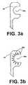
- FIG. 3 aillustrates the preferred embodiment for an aperture for connection with a package lead of the present invention
- FIG. 3 billustrates an alternative embodiment of an aperture for connection with a package lead of the present invention
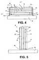
- FIG. 4illustrates a horizontally stacked module of the present invention
- FIG. 5illustrates a vertically stacked module of the present invention
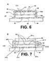
- FIG. 6illustrates an alternative embodiment of a horizontally stacked module of the present invention.
- FIG. 7illustrates an alternative embodiment of horizontally stacked module of the present invention.
- the letter of a reference character containing numerics followed by a lettereither identifies the relative placement of the numeric reference within a stacked module or it identifies a specific embodiment.
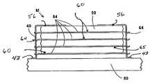
- a typical ball-grid-array package 50is comprised of an integrated circuit 51 surrounded by an essentially rectangular solid resin casing 55 .
- Package leads 52extend from the bottom surface 54 of the casing in a two-dimensional grid pattern providing electrical and thermal coupling to one or more integrated circuit die 51 that are embedded within the protective casing.
- the external portion of each package lead 52includes a coating of solder having a semi-spherical shape.
- the protective casing 55completely surrounds the embedded die but, in some ball-grid-array packages 50 , the protective casing 55 does not cover the inactive top surface 53 of the die.
- Near-chip scale packages 50provide 1.0 mm center-to-center spacing between leads 52 .
- Chip scale packagingsuch as MICRO_BGATM have center-to-center lead spacing of 0.5 mm. Chip scale packaging offers excellent electrical characteristics including low capacitance and thermal design.
- FIGS. 4 through 7show various specific embodiments of stacked module M of the present invention.
- the letter Mdesignates the module M formed of a plurality of ball-grid-array packages 50 .
- the packages 50are aligned as shown in FIGS. 4, 5 and 7 where the bottom surfaces 54 of each package 50 are facing the same direction.
- the packages 50may be aligned where one or more of the packages 50 are inverted in relation to the other packages 50 as shown in FIG. 6 .
- the top package 50 dis inverted with respect to the bottom package 50 e ; the top surface 53 of the top package 50 d is in substantially full contact with the adhesive 70 on the top surface 53 of the lower package 50 e.
- FIG. 1illustrates a partial cross-section of any two adjacent packages 50 that comprise a module M.
- the internals of package 50 bare not shown for simplicity.
- FIG. 1shows two packages 50 a and 50 b mounted on opposite sides of a lead carrier 60 comprised of a single thin copper plane.
- Interconnect leads 64extend away from the module M to provide external circuit connectivity to package leads 52 of the top package 50 a .
- External connectivitymay be provided in different configurations as described in detail below with reference to FIGS. 4-7 .
- FIG. 2A typical layout of a single plane lead carrier 60 is shown in FIG. 2 .
- the lead carrier 60is made to be flexible for increased reliability and ease of assembly.
- a lead carrier 60can be comprised of elongated conductive elements 65 formed from a thermally and electrically conductive thin planer material such as beryllium copper alloy C3 having a thickness of about 3 mils. Each conductive element 65 is defined to include a trace, interconnect pad, via and any other conductive feature of the lead carrier that are electrically coupled. Other preferred alloys for the lead-carrier-conductive elements 62 are full hard or hard copper alloys (110 or 197) or olin copper alloy 1094. Preferably, the lead carrier 60 is formed from custom flexible circuits from 3MTM and other manufacturers.
- These well known flexible circuitsare typically comprised of one or more thin (1.4 mils thick) layers of conductive material that are die cut and drilled to form apertures 66 , ground planes and conductive elements 65 which include traces, mounting pads and leads.
- the conductive layerstypically are flanked by a thin (typically 1 to 11 mill thick) layer of electrically-insulating, high-dielectric materials such at polyamide, polyester or teflon which results in circuit composites that are flexible.
- the material and thickness of individual layers that comprise the lead carriers 60 as well as spacing between conductive elements 65 and the width of conductive elements 65can be precisely controlled to provide a accurate and consistent impedance control in select conductive elements 65 .
- Lead carriers 60 formed from custom flexible-circuitscan have vias for connecting traces 65 located on different planes and conductive pads (or leads), with solder coating having footprints that are compatible with standards for ball-grid array packages 50 for electrical and mechanical coupling to a printed wiring board 80 .
- each conductive element 65 in a lead carrier 60has at least one aperture 66 , adapted to receive an individual package lead 52 and at least one interconnect portion 64 that extends away from the module to provide an external point of electrical connection to package leads 52 .
- Interconnect portions 64preferably have a spring-like resiliency for increased reliability.
- Apertures 66have about the same diameter as a package lead 52 allowing each package lead 52 to extend through the aperture 66 and for the lead carrier 60 to have substantial contact with the bottom surface 54 of a package 50 .
- FIG. 3 aillustrates the preferred semi-circle shape 66 a for the aperture 66 where the conductive element 65 partially surrounds the package ball 52 .
- the semicircle shape 66 aas opposed to a full-circle shape, enables an increased space for routing the conductive elements 65 of the lead carrier 60 .
- the present inventionutilizes standard manufactured packages 50 to form the multi-package module M.
- packages 50typically have package lead 52 irregularities or inconsistencies, particularly, lead length and solder coating variations. These variations make automated assembly problematic since the tolerances necessary to accommodate variation in lead 52 length, for example, do not permit the packages 50 to be assembled within the more stringent requirements for automated assembly of the module M.
- the package leads 52typically have excess solder that can cause electrical shorts between package leads 52 .
- the leads 52 of the ball-grid-array packages 50are scythed prior to assembly or as an automated step during the assembly after the lead carrier 60 is attached. Scything is the preferred method of reducing the length by which package leads 52 extend from the package 50 . Scything is a method where a hot razor knife skims off the distal portion of all package leads 52 .
- the adhesive 70may be epoxy, such as Rogers Corp. R/flex 8970 which is B-staged phenolic butyryl epoxy, that may be laminated at a temperature of 130 degrees centigrade and cured at a temperature of about 175 degrees centigrade.
- the preferred methodis to use a 2 mil thick sandwich of polyamide film 70 , such as KaptonTM which includes a 0.5 mil thick layer of adhesive on both sides (a three-layer system).
- a thermally conductive filled adhesive 70may be used to enhance the transfer of heat between adjacent packages 50 , and between the packages 50 and carrier 60 .
- a horizontally oriented embodiment of the present inventionis illustrated.
- a module Mis preassembled and then attached to a PWB 80 or other circuit carrying substrate.
- the preassembled module Mmay be inserted into an integrated circuit socket.
- each lead carrier 65has an external interconnect portion 64 which extends from both sides of the module M to provide interconnection to an electrically and thermally conductive external interconnect structure 40 .
- Structure 40provides mechanical rigidity to the module M and is adhered to the upper surface 41 of the uppermost package 50 .
- Structure 40also includes circuit board interconnection portions 43 which may be formed for industry-standard socketability with an electrical socket carried in circuit board substrate 80 .
- FIG. 5A vertically-oriented configuration of module M is illustrated in FIG. 5 .
- lead carriers 60are formed with external interconnect portions 64 all extending to one side which requires the conductive elements 65 to be more densely spaced.
- external interconnect portions 64are spaced in row and column configuration for socketing or soldering to circuit connections on circuit board substrate 80 .
- module Mis formed in a two-high stack comprised of packages 50 e and 50 d .
- package 50 ehas its package leads 52 mounted directly to corresponding array of external circuit connect pads carried in substrate 80 .
- Upper package 50 dis inverted with respect to package 50 e and mounted to package 50 d with thermally conductive adhesive layer 70 .
- Surface 54 of package 50 dincludes package leads 52 .
- a lead carrier 60formed as described above, is adhered to surface 54 of package 50 d with thermally conductive adhesive 70 .
- External circuit interconnect portions 64provide electrical connectivity for upper package 50 d to circuit connection pads carried in substrate 80 .
- module Mis shown in an alternative three-high configuration comprised of individual packages 50 a , 50 b and 50 c .
- a lead carrier 60is adhered to the package lead surface 54 of each package.
- package leads 52are not shown as to packages 50 a and 50 b .
- Lead carriers 60 for packages 50 a and 50 binclude external circuit connect portions 64 b which are formed to nest together to provide mechanical rigidity and electrical and thermal conductivity for the module M.
- Lower package 50 chas lead carrier 60 c adhered to its lower surface 54 in the manner described above with thermally conductivity, electrically insulating adhesive.
- circuit connection portions 64 a of lead carrier 60 care selectively interconnected to connection portions 64 b .
- Package leads 52 of lower package 50 care connected to external circuit connections carried in substrate 80 in a standard ball-grid-array pattern.
- a method for manufacture a module Minvolves the following steps: (1) mounting an adhesive 70 a to the bottom surface 56 of a package 50 ; (2) aligning and mounting a lead carrier 60 to the adhesive 70 wherein apertures 66 receive the package leads 52 ; (3) scything of the distal end of all package leads 52 ; (4) applying heat (about 175 degrees centigrade) to cure adhesive 70 and flow the package lead 52 solder coating; (5) mounting a second thin layer of adhesive 70 b to the lead carrier 60 ; and (6) mounting another package 50 to the adhesive 70 b , wherein the top surface 56 of the package 50 has substantial contact with the adhesive. Steps 1 though 6 are repeated for each package 50 added to the module, except steps 5 and 6 are not repeated for the last package 50 . For reliability and remanufacturability, it may be desirable to test each package 50 as it is added to the module M.
- the preferred methodreplaces the steps of applying adhesive 70 a and 70 b with the preliminary step of applying double-sided adhesive tape 70 to both upper and lower surfaces of each lead carrier 60 prior to assembly.
- the step of applying heat to cause solder 53 to flow and to cure adhesive 66 after each step of mounting a package 50is eliminated if the leads 52 of the package 50 are reduced in height prior to assembly and a thin area of the second layer of adhesive 70 b around each aperture 66 is left void to allow the package leads 52 to form a flange when heat is applied.
- the module Mmay be assembled using a suitably formed manufacturing jig provided to hold individual packages 50 in alignment as they are stacked together with interspaced lead carriers 60 and adhesive carrying tape 70 . In this embodiment, the entire module M may be preassembled and a single heating event applied to flow the solder and cure the adhesive 70 as pressure is exerted on the module M to compress the layers.
- FIG. 3 ban alternative embodiment which compensates for excess solder steps utilizes channels 66 c formed in each aperture 66 b .
- FIG. 3 billustrates one shape of an aperture 66 b with multiple channels 66 c .
- a channel 66 cis a void area in a conductive element 65 which merges into the void area of an aperture 66 .
- an edge of each channel 66 cis in close proximity to the package leads 52 .
- the void area of the channel 66 cextends away from the ball 52 .
- the external structure 40may be formed integral to the leads 64 extending from the lead carrier 61 as shown in FIGS. 6 and 7 .
- the leads 64 bare formed such to electrically and thermally connect directly to selected adjacent leads 64 b .
- Leads 64may be formed with a substrate mounting portion 65 that may have a standard “gull-wing,” “J-lead” shape.
Landscapes
- Engineering & Computer Science (AREA)
- Microelectronics & Electronic Packaging (AREA)
- Power Engineering (AREA)
- Physics & Mathematics (AREA)
- Condensed Matter Physics & Semiconductors (AREA)
- General Physics & Mathematics (AREA)
- Computer Hardware Design (AREA)
- Lead Frames For Integrated Circuits (AREA)
- Structures For Mounting Electric Components On Printed Circuit Boards (AREA)
Abstract
Description
- This application is a continuation-in-part of application Ser. No. 08/774,699, filed Dec. 26, 1996 and a Continuing Prosecution Application filed Feb. 11, 1998, pending, which is a continuation of 08/497,565, filed Jun. 30, 1995, now issued as U.S. Pat. No. 5,631,193, which is a continuation of application Ser. No. 07/990,334, filed Dec. 11, 1992, now issued as U.S. Pat. No. 5,484,959.
- 1. Field of the Invention
- This invention relates to a high density, integrated circuit module, which includes a plurality of vertically or horizontally stacked individual surface mount or ball-grid-array integrated circuit packages.
- 2. Brief Description of the Related Technology
- An example of a fabrication method and apparatus for high density lead-on-package modules by laminating one or more lead frames to standard integrated circuit packages is disclosed in U.S. Pat. No. 5,484,959, assigned to the common assignee of the present invention and incorporated herein by reference. Other methods for providing high density, stacked modules are disclosed in U.S. Pat. Nos. 5,279,029, 5,367,766, 5,455,740, 5,450,959 and 5,592,364, all of which are assigned to the common assignee of the present invention and incorporated herein by reference. The general methods and apparatus disclosed in the referenced patents can be applied to the fabrication of stacked configurations comprised of individual ball-grid-array or surface mount packages. However, the characteristic lead orientation, lead shape and lead content of ball-grid-array or surface mount packages impose a different set of parameters not adequately provided for by prior methods and assemblies.
- The present invention provides a novel method and apparatus for manufacturing three-dimensional, high density, integrated circuit modules from standard ball-grid-array or other surface mount integrated circuit packages which provides improved space efficiency and heat dissipation. One way to increase space efficiency is to stack individual packages. Generally speaking, higher density generates more localized heat and thus increases the need for efficient heat dissipation. Improving the thermal transfer characteristics of the individual integrated circuit packages results in better heat dissipation for the module, and improves reliability and durability.
- The present invention provides a novel method of fabricating a three-dimensional module formed of stacked and aligned surface mount or ball-grid-array packages. Ball-Grid-Array (BGA) integrated circuit packages typically have leads that extend from the bottom surface of a rectangular solid resin casing in a two-dimensional grid pattern. The external portion of each lead finished with a ball of solder. Package leads provide electrical and thermal coupling to one or more integrated circuit dies that are embedded within the protective casing. Typically, the protective casing completely surrounds the embedded die but, in some BGA packages, the protective casing does not cover the inactive top surface of the die. Near-chip scale packages provide 1.0 mm center-to-center lead spacing. Chip scale packaging such as MICRO_BGA™ have center-to-center lead spacing of 0.5 mm. Chip scale packaging offers excellent electrical characteristics including low capacitance and thermal design.
- Connectivity to the leads of individual packages in a module is provided by thin substantially planar lead carriers located between adjacent packages. Lead carriers are adhered to adjacent packages with a thermally conductive but electrically insulating adhesive. A lead carrier is comprised of elongated electrically and thermally conductive elements formed in one or more thin planes of conductive material that are separated by high-dielectric material. Typically, each conductive element has at least one aperture, adapted to receive and electrically couple to an individual package ball and at least one interconnect lead that extends away from the module to provide external circuit connectivity to package leads. Preferably, the lead carriers are formed from custom flexible circuits commercially available from 3M™ or other manufacturers. These well known flexible circuits are typically comprised of one or more thin layers of conductive material that are die cut and drilled to form ground planes, signal traces, pads and apertures. The conductive layers are typically embedded in and between electrically-insulating, high-dielectric material such as polyamide, polyester or teflon which results in circuits that are flexible, have dense trace, and provide accurate impedance control.
- The present invention utilizes standard manufactured packages to form the multi-package module. Such packages typically have ball irregularities or inconsistencies, particularly ball length and solder coating variations. These variations make automated assembly problematic since the tolerances necessary to accommodate variation in ball length and excess solder, for example, do not permit the packages to be assembled within the more stringent requirements for automated assembly of the module. According to one aspect of the present invention, the leads of the ball-grid-array packages are scythed prior to assembly or as an automated step during the assembly. Scything is a method where a hot razor knife skims off a layer from the distal end of all the leads of a ball-grid-array package, reducing random excess lead length and providing a uniform, closely tolerant lead length. The step of scything allows multiple packages to be added to the module prior to a final heating step where the solder for all the packages is flowed. This method also has the advantage of increasing the minimal tolerances for positioning of ball-grid-array package on the lead carrier. An alternative method that may also be used to compensate for excess solder from the leads is to provide channels formed in the walls or edges of each aperture of the lead carrier that receives the ball so the excess solder, when heated, flows into the channels A channel is a void area in a conductive element which merges into the void area of an aperture. An edge of the channel is in close proximity to the package leads and the void area extends away from the leads. Channels take advantage of the surface tension of molten solder which will pull molten solder away from leads to fill the channel.
- Another object of the present invention is to provide an assembly which effectively dissipates heat generated during normal operation. Efficient thermal management increases the operational life of the module, and improves reliability by eliminating the effects of elevated temperature on the electrical characteristics of the integrated circuit and packaging. When packages are not stacked, heat from the embedded integrated circuits, generated through normal operation, is primarily dissipated by convection from the package's external surfaces to the surrounding air. When modules are formed by stacking packages, the buried packages have reduced surface area exposed to the air. The use of thermally conductive adhesive facilitates the transmission of heat between adjacent packages and is an effective method of taking advantage of the exposed surfaces for removing heat from buried packages.
- In the module of the present invention, the package leads are thermally coupled to the lead carrier and provide a path for heat from the embedded integrated circuits. Thermally conductive adhesive also facilitates transfer of heat from packages to the lead carrier.
- In applications where it is desirable to reduce the package and module height, or where package or module warping is a concern, each package may be constructed using any of the various techniques described in U.S. Pat. Nos. 5,369,056, 5,369,058 and 5,644,161, each of which is assigned to the common assignee of the present invention and incorporated herein by reference. These patents describe methods for constructing thin, durable packages and modules with enhanced heat dissipation characteristics and minimal warpage.
- A common application of a stacked configuration is memory modules. Most of the leads of each package are electrically connected to corresponding leads of adjacent packages. A method is required to select the individual memory package being read, written or refreshed. One method is to provide a custom manufactured lead carrier for each package. A more cost-effective method is to use a common lead carrier design with extra package interconnect leads which is then modified by clipping off or no-connecting selected interconnect leads to make each lead carrier in a stacked configuration unique. Methods for connecting a unique bit of a data word per package and for uniquely addressing each package in a stacked configuration are described in U.S. Pat. Nos. 5,279,029 and 5,371,866, both which are assigned to the common assignee of the present invention and incorporated herein by reference. While the apparatus and methods of the present invention are described herein with reference to standard, single-size packages, it will be appreciated by those of ordinary skill in the art, that those methods and apparatus are equally applicable to multiple-die packages.
FIG. 1 is a cross-sectional view of two adjacent packages of a module of the present invention;FIG. 2 is a top planar view of a typical lead carrier of the present invention;FIG. 3 aillustrates the preferred embodiment for an aperture for connection with a package lead of the present invention;FIG. 3 billustrates an alternative embodiment of an aperture for connection with a package lead of the present invention;FIG. 4 illustrates a horizontally stacked module of the present invention;FIG. 5 illustrates a vertically stacked module of the present invention;FIG. 6 illustrates an alternative embodiment of a horizontally stacked module of the present invention; andFIG. 7 illustrates an alternative embodiment of horizontally stacked module of the present invention.- Other and further objects, features and advantages will be apparent from the following description of the preferred embodiments of the invention, given for the purpose of disclosure and taken in conjunction with the accompanying drawings.
- The letter of a reference character containing numerics followed by a letter, either identifies the relative placement of the numeric reference within a stacked module or it identifies a specific embodiment.
- Referring now to
FIG. 1 , a typical ball-grid-array package 50 is comprised of anintegrated circuit 51 surrounded by an essentially rectangularsolid resin casing 55. Package leads52 extend from thebottom surface 54 of the casing in a two-dimensional grid pattern providing electrical and thermal coupling to one or more integrated circuit die51 that are embedded within the protective casing. The external portion of eachpackage lead 52 includes a coating of solder having a semi-spherical shape. Typically, theprotective casing 55 completely surrounds the embedded die but, in some ball-grid-array packages 50, theprotective casing 55 does not cover the inactivetop surface 53 of the die. Near-chip scale packages50 provide 1.0 mm center-to-center spacing between leads52. Chip scale packaging such as MICRO_BGA™ have center-to-center lead spacing of 0.5 mm. Chip scale packaging offers excellent electrical characteristics including low capacitance and thermal design. FIGS. 4 through 7 show various specific embodiments of stacked module M of the present invention. The letter M designates the module M formed of a plurality of ball-grid-array packages50. Typically, thepackages 50 are aligned as shown inFIGS. 4, 5 and7 where the bottom surfaces54 of eachpackage 50 are facing the same direction. Alternately, thepackages 50 may be aligned where one or more of thepackages 50 are inverted in relation to theother packages 50 as shown inFIG. 6 . In this embodiment, thetop package 50dis inverted with respect to thebottom package 50e; thetop surface 53 of thetop package 50dis in substantially full contact with the adhesive70 on thetop surface 53 of thelower package 50e.- A typical application of one aspect of the present invention is shown in
FIG. 1 which illustrates a partial cross-section of any twoadjacent packages 50 that comprise a module M. The internals ofpackage 50bare not shown for simplicity.FIG. 1 shows twopackages lead carrier 60 comprised of a single thin copper plane. Interconnect leads64 extend away from the module M to provide external circuit connectivity to package leads52 of thetop package 50a. External connectivity may be provided in different configurations as described in detail below with reference toFIGS. 4-7 . A typical layout of a singleplane lead carrier 60 is shown inFIG. 2 . Thelead carrier 60 is made to be flexible for increased reliability and ease of assembly. Alead carrier 60 can be comprised of elongatedconductive elements 65 formed from a thermally and electrically conductive thin planer material such as beryllium copper alloy C3 having a thickness of about 3 mils. Eachconductive element 65 is defined to include a trace, interconnect pad, via and any other conductive feature of the lead carrier that are electrically coupled. Other preferred alloys for the lead-carrier-conductive elements62 are full hard or hard copper alloys (110 or 197) or olin copper alloy 1094. Preferably, thelead carrier 60 is formed from custom flexible circuits from 3M™ and other manufacturers. These well known flexible circuits are typically comprised of one or more thin (1.4 mils thick) layers of conductive material that are die cut and drilled to formapertures 66, ground planes andconductive elements 65 which include traces, mounting pads and leads. The conductive layers typically are flanked by a thin (typically 1 to 11 mill thick) layer of electrically-insulating, high-dielectric materials such at polyamide, polyester or teflon which results in circuit composites that are flexible. The material and thickness of individual layers that comprise thelead carriers 60 as well as spacing betweenconductive elements 65 and the width ofconductive elements 65 can be precisely controlled to provide a accurate and consistent impedance control in selectconductive elements 65. Leadcarriers 60 formed from custom flexible-circuits can have vias for connectingtraces 65 located on different planes and conductive pads (or leads), with solder coating having footprints that are compatible with standards for ball-grid array packages50 for electrical and mechanical coupling to a printedwiring board 80. - Typically, each
conductive element 65 in alead carrier 60 has at least oneaperture 66, adapted to receive anindividual package lead 52 and at least oneinterconnect portion 64 that extends away from the module to provide an external point of electrical connection to package leads52.Interconnect portions 64 preferably have a spring-like resiliency for increased reliability.Apertures 66 have about the same diameter as apackage lead 52 allowing eachpackage lead 52 to extend through theaperture 66 and for thelead carrier 60 to have substantial contact with thebottom surface 54 of apackage 50. The application of heat (about 175 degrees centigrade) that is sufficient to cause the solder comprising the package leads52 to flow will cause the solder to adhere to a thin area of aconductive element 65 on the surface of thelead carrier 60 facing away from thepackage 50 that surrounds eachaperture 66 to formflange 55 that provides excellent electrical and mechanical coupling between package leads52 and thelead carrier 60.FIG. 3 aillustrates the preferredsemi-circle shape 66afor theaperture 66 where theconductive element 65 partially surrounds thepackage ball 52. The semicircle shape66a, as opposed to a full-circle shape, enables an increased space for routing theconductive elements 65 of thelead carrier 60. - The present invention utilizes standard manufactured
packages 50 to form the multi-package module M. Such packages50 typically havepackage lead 52 irregularities or inconsistencies, particularly, lead length and solder coating variations. These variations make automated assembly problematic since the tolerances necessary to accommodate variation inlead 52 length, for example, do not permit thepackages 50 to be assembled within the more stringent requirements for automated assembly of the module M. The package leads52 typically have excess solder that can cause electrical shorts between package leads52. According to one aspect of the present invention, theleads 52 of the ball-grid-array packages 50 are scythed prior to assembly or as an automated step during the assembly after thelead carrier 60 is attached. Scything is the preferred method of reducing the length by which package leads52 extend from thepackage 50. Scything is a method where a hot razor knife skims off the distal portion of all package leads52. - Referring again to
FIG. 1 , leadcarriers 60 are adhered toadjacent packages 50 with a thermally conductive but electrical-insulatingadhesive 70. The adhesive70 may be epoxy, such as Rogers Corp. R/flex 8970 which is B-staged phenolic butyryl epoxy, that may be laminated at a temperature of 130 degrees centigrade and cured at a temperature of about 175 degrees centigrade. The preferred method is to use a 2 mil thick sandwich ofpolyamide film 70, such as Kapton™ which includes a 0.5 mil thick layer of adhesive on both sides (a three-layer system). A thermally conductive filled adhesive70 may be used to enhance the transfer of heat betweenadjacent packages 50, and between thepackages 50 andcarrier 60. - Referring now to
FIG. 4 , a horizontally oriented embodiment of the present invention is illustrated. Typically, a module M is preassembled and then attached to aPWB 80 or other circuit carrying substrate. Alternately, the preassembled module M may be inserted into an integrated circuit socket. - In
FIG. 4 , a plurality of integrated circuit packages50, each with an attachedlead carrier 65, are stacked in a horizontally-oriented module M. In this configuration, eachlead carrier 65 has anexternal interconnect portion 64 which extends from both sides of the module M to provide interconnection to an electrically and thermally conductiveexternal interconnect structure 40.Structure 40 provides mechanical rigidity to the module M and is adhered to the upper surface41 of theuppermost package 50.Structure 40 also includes circuitboard interconnection portions 43 which may be formed for industry-standard socketability with an electrical socket carried incircuit board substrate 80. - A vertically-oriented configuration of module M is illustrated in
FIG. 5 . In this embodiment,lead carriers 60 are formed withexternal interconnect portions 64 all extending to one side which requires theconductive elements 65 to be more densely spaced. In this embodiment,external interconnect portions 64 are spaced in row and column configuration for socketing or soldering to circuit connections oncircuit board substrate 80. - Another embodiment of module M is illustrated with reference to
FIG. 6 . In this embodiment, module M is formed in a two-high stack comprised ofpackages package 50ehas its package leads52 mounted directly to corresponding array of external circuit connect pads carried insubstrate 80.Upper package 50dis inverted with respect to package50eand mounted to package50dwith thermally conductiveadhesive layer 70.Surface 54 ofpackage 50dincludes package leads52. Alead carrier 60, formed as described above, is adhered to surface54 ofpackage 50dwith thermallyconductive adhesive 70. Externalcircuit interconnect portions 64 provide electrical connectivity forupper package 50dto circuit connection pads carried insubstrate 80. - Referring now to
FIG. 7 , module M is shown in an alternative three-high configuration comprised ofindividual packages lead carrier 60 is adhered to thepackage lead surface 54 of each package. For clarity, package leads52 are not shown as topackages carriers 60 forpackages portions 64bwhich are formed to nest together to provide mechanical rigidity and electrical and thermal conductivity for the moduleM. Lower package 50chas lead carrier60cadhered to itslower surface 54 in the manner described above with thermally conductivity, electrically insulating adhesive. In this embodiment,circuit connection portions 64aof lead carrier60care selectively interconnected toconnection portions 64b. Package leads52 oflower package 50care connected to external circuit connections carried insubstrate 80 in a standard ball-grid-array pattern. - According to one specific method of the present invention, a method for manufacture a module M involves the following steps: (1) mounting an adhesive70ato the
bottom surface 56 of apackage 50; (2) aligning and mounting alead carrier 60 to the adhesive70 whereinapertures 66 receive the package leads52; (3) scything of the distal end of all package leads52; (4) applying heat (about 175 degrees centigrade) to cure adhesive70 and flow thepackage lead 52 solder coating; (5) mounting a second thin layer of adhesive70bto thelead carrier 60; and (6) mounting anotherpackage 50 to the adhesive70b, wherein thetop surface 56 of thepackage 50 has substantial contact with the adhesive. Steps1 though6 are repeated for eachpackage 50 added to the module, except steps5 and6 are not repeated for thelast package 50. For reliability and remanufacturability, it may be desirable to test eachpackage 50 as it is added to the module M. - The preferred method replaces the steps of applying adhesive70aand70bwith the preliminary step of applying double-sided
adhesive tape 70 to both upper and lower surfaces of eachlead carrier 60 prior to assembly. The step of applying heat to causesolder 53 to flow and to cure adhesive66 after each step of mounting apackage 50 is eliminated if the leads52 of thepackage 50 are reduced in height prior to assembly and a thin area of the second layer of adhesive70baround eachaperture 66 is left void to allow the package leads52 to form a flange when heat is applied. The module M may be assembled using a suitably formed manufacturing jig provided to holdindividual packages 50 in alignment as they are stacked together with interspacedlead carriers 60 and adhesive carryingtape 70. In this embodiment, the entire module M may be preassembled and a single heating event applied to flow the solder and cure the adhesive70 as pressure is exerted on the module M to compress the layers. - Referring now to
FIG. 3 b, an alternative embodiment which compensates for excess solder steps utilizeschannels 66cformed in eachaperture 66b.FIG. 3 billustrates one shape of anaperture 66bwithmultiple channels 66c. Achannel 66cis a void area in aconductive element 65 which merges into the void area of anaperture 66. When apackage lead 52 is inserted into theaperture 66b, an edge of eachchannel 66cis in close proximity to the package leads52. The void area of thechannel 66cextends away from theball 52. When heat is applied such that the solder coating the package leads52 becomes molten, excess solder is pulled by the inherent surface tension of molten solder to fill the voided area. - Communication between individual integrated circuits embedded within
packages 50 and signals external to the modules are provided by various methods for implementing an external structure. Methods and apparatus of such structures are described in U.S. Pat. Nos. 5,279,029 and 5,367,766. Alternatively, theexternal structure 40 may be formed integral to theleads 64 extending from the lead carrier61 as shown inFIGS. 6 and 7 . In the embodiment shown inFIG. 7 , theleads 64bare formed such to electrically and thermally connect directly to selectedadjacent leads 64b. Leads64 may be formed with asubstrate mounting portion 65 that may have a standard “gull-wing,” “J-lead” shape. - The foregoing disclosure and description of the invention are illustrative and explanatory of the preferred embodiments. Changes in the size, shape, materials and individual components used, elements, connections and construction may be made without departing from the spirit of the invention.
Claims (11)
1-41. (canceled)
42. A high density circuit module comprising:
first and second BGA packages, each having a body exhibiting a bottom surface, a top surface, a plurality of BGA contacts arranged in a grid along the bottom surface and first and second opposing lateral sides;
a flexible circuit having a first side with a first BGA-connecting portion including a plurality of electrical contacts arranged in a grid, and a second side, the first BGA-connecting portion of the first side of the flexible circuit being disposed below the body of the first BGA package and connected through the plurality of electrical contacts to the plurality of BGA contacts of the first BGA, the flexible circuit having a second portion having a second portion set of contacts for connecting to a circuit board and a third portion having a third portion set of contacts for connecting to the circuit board, the second portion being disposed partially beside the first lateral side of the second BGA package and the third portion being disposed partially beside the second lateral side of the second BGA package to dispose the second portion set of contacts and the third portion set of contacts below the level of a plane defined by the bottom surface of the body of the second BGA package.
43. The high density circuit module ofclaim 42 in which the flexible circuit comprises two or more planes of conductive material separated by high dielectric material.
44. The high density circuit module ofclaim 42 in which the plurality of electrical contacts are each formed having an aperture adapted to receive one of the BGA contacts.
45. The high density circuit module ofclaim 42 in which the flexible circuit is adhesively connected to the top surface of the second selected BGA package.
46. A high density circuit module comprising:
a first BGA package having a body with a bottom surface, a top surface, a plurality of BGA contacts arranged in a grid along the bottom surface, and first and second opposing lateral sides that define a vertical extent of body;
a first flexible circuit having a first portion disposed above the top surface of the first BGA package, the first portion having a grid of electrical contacts, a second portion disposed beside the first lateral side of the first BGA package, a third portion disposed beside the second lateral side of the first BGA package, a fourth portion disposed adjacent to the second portion and below the vertical extent of the body of the first BGA package, the fourth portion having a first set of contacts for connecting to a circuit board, a fifth portion disposed adjacent to the third portion and below the vertical extent of the body of the first BGA package, the fifth portion having a second set of contacts for connecting to the circuit board;
a second BGA package having a body with a bottom surface, a top surface, a plurality of BGA contacts arranged in a grid along the bottom surface, and first and second opposing lateral sides that define a vertical extent of body, the second BGA package being mounted to the grid of electrical contacts, the second BGA package being above the first BGA package.
47. The high density circuit module ofclaim 46 in which the first flexible circuit comprises two or more planes of conductive material separated by high dielectric material.
48. The high density circuit module ofclaim 46 further comprising:
a second flexible circuit having a first portion disposed above the top surface of the second BGA package, the first portion having a grid of electrical contacts, a second portion disposed beside the first lateral side of the second BGA package, a third portion disposed beside the second lateral side of the second BGA package, a fourth portion disposed adjacent to the second portion and below the vertical extent of the body of the second BGA package, the fourth portion having a first set of contacts for connecting to the first flexible circuit, a fifth portion disposed adjacent to the third portion and below the vertical extent of the body of the second BGA package, the fifth portion having a second set of contacts for connecting to the first flexible circuit;
a third BGA package having a body with a bottom surface, a top surface, a plurality of BGA contacts arranged in a grid along the bottom surface, and first and second opposing lateral sides that define a vertical extent of body, the third BGA package being mounted to the grid of electrical contacts of the second flexible circuit, the third BGA package being above the second BGA package.
49. The high density circuit module ofclaim 46 in which the grid of electrical contacts are each formed having an aperature adapted to receive one of the BGA contacts.
50. The high density circuit module ofclaim 46 in which the flexible circuit is adhesively connected to the top surface of the second selected BGA package.
51. The high density circuit module ofclaim 46 in which the flexible circuit is adhesively connected to the top surface of the second selected BGA package.
Priority Applications (1)
| Application Number | Priority Date | Filing Date | Title |
|---|---|---|---|
| US11/040,564US20050139980A1 (en) | 1992-12-11 | 2005-01-21 | High density integrated circuit module |
Applications Claiming Priority (5)
| Application Number | Priority Date | Filing Date | Title |
|---|---|---|---|
| US07/990,334US5484959A (en) | 1992-12-11 | 1992-12-11 | High density lead-on-package fabrication method and apparatus |
| US08/497,565US5631193A (en) | 1992-12-11 | 1995-06-30 | High density lead-on-package fabrication method |
| US77469996A | 1996-12-26 | 1996-12-26 | |
| US09/761,210US6919626B2 (en) | 1992-12-11 | 2001-01-16 | High density integrated circuit module |
| US11/040,564US20050139980A1 (en) | 1992-12-11 | 2005-01-21 | High density integrated circuit module |
Related Parent Applications (1)
| Application Number | Title | Priority Date | Filing Date |
|---|---|---|---|
| US09/761,210ContinuationUS6919626B2 (en) | 1992-12-11 | 2001-01-16 | High density integrated circuit module |
Publications (1)
| Publication Number | Publication Date |
|---|---|
| US20050139980A1true US20050139980A1 (en) | 2005-06-30 |
Family
ID=25536047
Family Applications (3)
| Application Number | Title | Priority Date | Filing Date |
|---|---|---|---|
| US07/990,334Expired - LifetimeUS5484959A (en) | 1992-12-11 | 1992-12-11 | High density lead-on-package fabrication method and apparatus |
| US08/497,565Expired - Fee RelatedUS5631193A (en) | 1992-12-11 | 1995-06-30 | High density lead-on-package fabrication method |
| US11/040,564AbandonedUS20050139980A1 (en) | 1992-12-11 | 2005-01-21 | High density integrated circuit module |
Family Applications Before (2)
| Application Number | Title | Priority Date | Filing Date |
|---|---|---|---|
| US07/990,334Expired - LifetimeUS5484959A (en) | 1992-12-11 | 1992-12-11 | High density lead-on-package fabrication method and apparatus |
| US08/497,565Expired - Fee RelatedUS5631193A (en) | 1992-12-11 | 1995-06-30 | High density lead-on-package fabrication method |
Country Status (1)
| Country | Link |
|---|---|
| US (3) | US5484959A (en) |
Cited By (5)
| Publication number | Priority date | Publication date | Assignee | Title |
|---|---|---|---|---|
| US20070045818A1 (en)* | 2005-08-25 | 2007-03-01 | Kuan Lee C | Land grid array semiconductor device packages, assemblies including same, and methods of fabrication |
| US7465607B2 (en) | 2005-08-25 | 2008-12-16 | Micron Technology, Inc. | Methods of fabrication of lead frame-based semiconductor device packages incorporating at least one land grid array package |
| WO2009023781A1 (en)* | 2007-08-14 | 2009-02-19 | Shoppertrak Rct Corporation | Holding apparatus for a camera lens |
| US20130134568A1 (en)* | 2011-11-29 | 2013-05-30 | Silergy Semiconductor Technology (Hangzhou) Ltd | Lead frame and flip chip package device thereof |
| US10056324B2 (en) | 2016-11-09 | 2018-08-21 | International Business Machines Corporation | Trace/via hybrid structure with thermally and electrically conductive support material for increased thermal and electrical performance |
Families Citing this family (129)
| Publication number | Priority date | Publication date | Assignee | Title |
|---|---|---|---|---|
| US5702985A (en)* | 1992-06-26 | 1997-12-30 | Staktek Corporation | Hermetically sealed ceramic integrated circuit heat dissipating package fabrication method |
| US6205654B1 (en) | 1992-12-11 | 2001-03-27 | Staktek Group L.P. | Method of manufacturing a surface mount package |
| US5484959A (en)* | 1992-12-11 | 1996-01-16 | Staktek Corporation | High density lead-on-package fabrication method and apparatus |
| US5552563A (en)* | 1995-03-17 | 1996-09-03 | Sharp Microelectronics Technology, Inc. | Shielded low noise multi-lead contact |
| US6097099A (en)* | 1995-10-20 | 2000-08-01 | Texas Instruments Incorporated | Electro-thermal nested die-attach design |
| US5952725A (en) | 1996-02-20 | 1999-09-14 | Micron Technology, Inc. | Stacked semiconductor devices |
| JPH09307058A (en)* | 1996-05-14 | 1997-11-28 | Hitachi Ltd | Semiconductor device and electronic device using the same |
| US6784023B2 (en)* | 1996-05-20 | 2004-08-31 | Micron Technology, Inc. | Method of fabrication of stacked semiconductor devices |
| US5817530A (en)* | 1996-05-20 | 1998-10-06 | Micron Technology, Inc. | Use of conductive lines on the back side of wafers and dice for semiconductor interconnects |
| US5917242A (en)* | 1996-05-20 | 1999-06-29 | Micron Technology, Inc. | Combination of semiconductor interconnect |
| US6072228A (en)* | 1996-10-25 | 2000-06-06 | Micron Technology, Inc. | Multi-part lead frame with dissimilar materials and method of manufacturing |
| US6028352A (en) | 1997-06-13 | 2000-02-22 | Irvine Sensors Corporation | IC stack utilizing secondary leadframes |
| US6014316A (en)* | 1997-06-13 | 2000-01-11 | Irvine Sensors Corporation | IC stack utilizing BGA contacts |
| US6342731B1 (en)* | 1997-12-31 | 2002-01-29 | Micron Technology, Inc. | Vertically mountable semiconductor device, assembly, and methods |
| US6207474B1 (en) | 1998-03-09 | 2001-03-27 | Micron Technology, Inc. | Method of forming a stack of packaged memory die and resulting apparatus |
| US6404662B1 (en)* | 1998-03-23 | 2002-06-11 | Staktek Group, L.P. | Rambus stakpak |
| US6297548B1 (en)* | 1998-06-30 | 2001-10-02 | Micron Technology, Inc. | Stackable ceramic FBGA for high thermal applications |
| JP3035534B2 (en) | 1998-07-23 | 2000-04-24 | 敬 錫 姜 | Laminated package and method of laminating the same |
| US6179659B1 (en)* | 1998-08-11 | 2001-01-30 | Micron Technology, Inc. | Electrical contact device and associated method of manufacture |
| US6153929A (en) | 1998-08-21 | 2000-11-28 | Micron Technology, Inc. | Low profile multi-IC package connector |
| US6261865B1 (en) | 1998-10-06 | 2001-07-17 | Micron Technology, Inc. | Multi chip semiconductor package and method of construction |
| IL143962A0 (en)* | 1999-01-08 | 2002-04-21 | Emisphere Tech Inc | Polymeric delivery agents and delivery agent compounds |
| US6815251B1 (en) | 1999-02-01 | 2004-11-09 | Micron Technology, Inc. | High density modularity for IC's |
| US6323060B1 (en) | 1999-05-05 | 2001-11-27 | Dense-Pac Microsystems, Inc. | Stackable flex circuit IC package and method of making same |
| US6849480B1 (en) | 1999-05-07 | 2005-02-01 | Seagate Technology Llc | Surface mount IC stacking method and device |
| DE19983953T1 (en)* | 1999-05-07 | 2002-06-20 | Seagate Technology Llc | Method and device for stacking surface mount ICs |
| DE19933265A1 (en)* | 1999-07-15 | 2001-02-01 | Siemens Ag | TSOP memory chip package assembly |
| US6572387B2 (en) | 1999-09-24 | 2003-06-03 | Staktek Group, L.P. | Flexible circuit connector for stacked chip module |
| US6683372B1 (en)* | 1999-11-18 | 2004-01-27 | Sun Microsystems, Inc. | Memory expansion module with stacked memory packages and a serial storage unit |
| US6262895B1 (en) | 2000-01-13 | 2001-07-17 | John A. Forthun | Stackable chip package with flex carrier |
| DE10006445C2 (en)* | 2000-02-14 | 2002-03-28 | Infineon Technologies Ag | Intermediate frame for a housing frame of semiconductor chips |
| US6608763B1 (en) | 2000-09-15 | 2003-08-19 | Staktek Group L.P. | Stacking system and method |
| US7262082B1 (en) | 2000-10-13 | 2007-08-28 | Bridge Semiconductor Corporation | Method of making a three-dimensional stacked semiconductor package with a metal pillar and a conductive interconnect in an encapsulant aperture |
| US7009297B1 (en) | 2000-10-13 | 2006-03-07 | Bridge Semiconductor Corporation | Semiconductor chip assembly with embedded metal particle |
| US7129113B1 (en) | 2000-10-13 | 2006-10-31 | Bridge Semiconductor Corporation | Method of making a three-dimensional stacked semiconductor package with a metal pillar in an encapsulant aperture |
| US6486535B2 (en)* | 2001-03-20 | 2002-11-26 | Advanced Semiconductor Engineering, Inc. | Electronic package with surface-mountable device built therein |
| US6462408B1 (en) | 2001-03-27 | 2002-10-08 | Staktek Group, L.P. | Contact member stacking system and method |
| US6707684B1 (en) | 2001-04-02 | 2004-03-16 | Advanced Micro Devices, Inc. | Method and apparatus for direct connection between two integrated circuits via a connector |
| US6828884B2 (en)* | 2001-05-09 | 2004-12-07 | Science Applications International Corporation | Phase change control devices and circuits for guiding electromagnetic waves employing phase change control devices |
| US7145254B2 (en)* | 2001-07-26 | 2006-12-05 | Denso Corporation | Transfer-molded power device and method for manufacturing transfer-molded power device |
| US6607942B1 (en)* | 2001-07-26 | 2003-08-19 | Taiwan Semiconductor Manufacturing Company | Method of fabricating as grooved heat spreader for stress reduction in an IC package |
| US6618257B1 (en)* | 2001-07-27 | 2003-09-09 | Staktek Group, L.P. | Wide data path stacking system and method |
| US6451626B1 (en) | 2001-07-27 | 2002-09-17 | Charles W.C. Lin | Three-dimensional stacked semiconductor package |
| US6765287B1 (en) | 2001-07-27 | 2004-07-20 | Charles W. C. Lin | Three-dimensional stacked semiconductor package |
| US7053478B2 (en)* | 2001-10-26 | 2006-05-30 | Staktek Group L.P. | Pitch change and chip scale stacking system |
| US7026708B2 (en) | 2001-10-26 | 2006-04-11 | Staktek Group L.P. | Low profile chip scale stacking system and method |
| US6576992B1 (en) | 2001-10-26 | 2003-06-10 | Staktek Group L.P. | Chip scale stacking system and method |
| US7485951B2 (en)* | 2001-10-26 | 2009-02-03 | Entorian Technologies, Lp | Modularized die stacking system and method |
| US6956284B2 (en) | 2001-10-26 | 2005-10-18 | Staktek Group L.P. | Integrated circuit stacking system and method |
| US7310458B2 (en) | 2001-10-26 | 2007-12-18 | Staktek Group L.P. | Stacked module systems and methods |
| US6940729B2 (en)* | 2001-10-26 | 2005-09-06 | Staktek Group L.P. | Integrated circuit stacking system and method |
| US7202555B2 (en)* | 2001-10-26 | 2007-04-10 | Staktek Group L.P. | Pitch change and chip scale stacking system and method |
| US7371609B2 (en)* | 2001-10-26 | 2008-05-13 | Staktek Group L.P. | Stacked module systems and methods |
| US20040195666A1 (en)* | 2001-10-26 | 2004-10-07 | Julian Partridge | Stacked module systems and methods |
| US20060255446A1 (en)* | 2001-10-26 | 2006-11-16 | Staktek Group, L.P. | Stacked modules and method |
| US20050056921A1 (en)* | 2003-09-15 | 2005-03-17 | Staktek Group L.P. | Stacked module systems and methods |
| US20050009234A1 (en)* | 2001-10-26 | 2005-01-13 | Staktek Group, L.P. | Stacked module systems and methods for CSP packages |
| US6914324B2 (en)* | 2001-10-26 | 2005-07-05 | Staktek Group L.P. | Memory expansion and chip scale stacking system and method |
| US7656678B2 (en) | 2001-10-26 | 2010-02-02 | Entorian Technologies, Lp | Stacked module systems |
| US20030234443A1 (en) | 2001-10-26 | 2003-12-25 | Staktek Group, L.P. | Low profile stacking system and method |
| US6486549B1 (en) | 2001-11-10 | 2002-11-26 | Bridge Semiconductor Corporation | Semiconductor module with encapsulant base |
| US7081373B2 (en)* | 2001-12-14 | 2006-07-25 | Staktek Group, L.P. | CSP chip stack with flex circuit |
| US7190060B1 (en) | 2002-01-09 | 2007-03-13 | Bridge Semiconductor Corporation | Three-dimensional stacked semiconductor package device with bent and flat leads and method of making same |
| US6891276B1 (en) | 2002-01-09 | 2005-05-10 | Bridge Semiconductor Corporation | Semiconductor package device |
| US6690088B2 (en) | 2002-01-31 | 2004-02-10 | Macintyre Donald M. | Integrated circuit package stacking structure |
| US7242082B2 (en) | 2002-02-07 | 2007-07-10 | Irvine Sensors Corp. | Stackable layer containing ball grid array package |
| US6731011B2 (en) | 2002-02-19 | 2004-05-04 | Matrix Semiconductor, Inc. | Memory module having interconnected and stacked integrated circuits |
| KR20040007883A (en)* | 2002-07-11 | 2004-01-28 | 주식회사 썬더스 | Lead frame for stacked semiconductor packages, stacked semiconductor packages using it, and fabrication method thereof |
| US20040108583A1 (en)* | 2002-12-05 | 2004-06-10 | Roeters Glen E. | Thin scale outline package stack |
| US6841029B2 (en)* | 2003-03-27 | 2005-01-11 | Advanced Cardiovascular Systems, Inc. | Surface modification of expanded ultra high molecular weight polyethylene (eUHMWPE) for improved bondability |
| US20040245615A1 (en)* | 2003-06-03 | 2004-12-09 | Staktek Group, L.P. | Point to point memory expansion system and method |
| US7542304B2 (en)* | 2003-09-15 | 2009-06-02 | Entorian Technologies, Lp | Memory expansion and integrated circuit stacking system and method |
| US7993983B1 (en) | 2003-11-17 | 2011-08-09 | Bridge Semiconductor Corporation | Method of making a semiconductor chip assembly with chip and encapsulant grinding |
| US7227249B1 (en) | 2003-12-24 | 2007-06-05 | Bridge Semiconductor Corporation | Three-dimensional stacked semiconductor package with chips on opposite sides of lead |
| US20060033187A1 (en)* | 2004-08-12 | 2006-02-16 | Staktek Group, L.P. | Rugged CSP module system and method |
| US20060043558A1 (en)* | 2004-09-01 | 2006-03-02 | Staktek Group L.P. | Stacked integrated circuit cascade signaling system and method |
| US20060053345A1 (en)* | 2004-09-03 | 2006-03-09 | Staktek Group L.P. | Thin module system and method |
| US7542297B2 (en) | 2004-09-03 | 2009-06-02 | Entorian Technologies, Lp | Optimized mounting area circuit module system and method |
| US7443023B2 (en) | 2004-09-03 | 2008-10-28 | Entorian Technologies, Lp | High capacity thin module system |
| US7468893B2 (en) | 2004-09-03 | 2008-12-23 | Entorian Technologies, Lp | Thin module system and method |
| US7289327B2 (en) | 2006-02-27 | 2007-10-30 | Stakick Group L.P. | Active cooling methods and apparatus for modules |
| US7606049B2 (en) | 2004-09-03 | 2009-10-20 | Entorian Technologies, Lp | Module thermal management system and method |
| US7616452B2 (en) | 2004-09-03 | 2009-11-10 | Entorian Technologies, Lp | Flex circuit constructions for high capacity circuit module systems and methods |
| US7760513B2 (en) | 2004-09-03 | 2010-07-20 | Entorian Technologies Lp | Modified core for circuit module system and method |
| US20060050492A1 (en) | 2004-09-03 | 2006-03-09 | Staktek Group, L.P. | Thin module system and method |
| US7579687B2 (en)* | 2004-09-03 | 2009-08-25 | Entorian Technologies, Lp | Circuit module turbulence enhancement systems and methods |
| US7522421B2 (en)* | 2004-09-03 | 2009-04-21 | Entorian Technologies, Lp | Split core circuit module |
| US7606050B2 (en) | 2004-09-03 | 2009-10-20 | Entorian Technologies, Lp | Compact module system and method |
| US7606040B2 (en) | 2004-09-03 | 2009-10-20 | Entorian Technologies, Lp | Memory module system and method |
| US7511968B2 (en) | 2004-09-03 | 2009-03-31 | Entorian Technologies, Lp | Buffered thin module system and method |
| US7446410B2 (en)* | 2004-09-03 | 2008-11-04 | Entorian Technologies, Lp | Circuit module with thermal casing systems |
| US7324352B2 (en) | 2004-09-03 | 2008-01-29 | Staktek Group L.P. | High capacity thin module system and method |
| US7423885B2 (en) | 2004-09-03 | 2008-09-09 | Entorian Technologies, Lp | Die module system |
| US20060055024A1 (en)* | 2004-09-14 | 2006-03-16 | Staktek Group, L.P. | Adapted leaded integrated circuit module |
| US20060072297A1 (en)* | 2004-10-01 | 2006-04-06 | Staktek Group L.P. | Circuit Module Access System and Method |
| US20060118936A1 (en)* | 2004-12-03 | 2006-06-08 | Staktek Group L.P. | Circuit module component mounting system and method |
| US7309914B2 (en)* | 2005-01-20 | 2007-12-18 | Staktek Group L.P. | Inverted CSP stacking system and method |
| US20060170094A1 (en)* | 2005-02-02 | 2006-08-03 | Intel Corporation | Semiconductor package integral heat spreader |
| US20060175693A1 (en)* | 2005-02-04 | 2006-08-10 | Staktek Group, L.P. | Systems, methods, and apparatus for generating ball-out matrix configuration output for a flex circuit |
| US7388280B2 (en)* | 2005-02-22 | 2008-06-17 | Stats Chippac Ltd. | Package stacking lead frame system |
| US7033861B1 (en) | 2005-05-18 | 2006-04-25 | Staktek Group L.P. | Stacked module systems and method |
| US7576995B2 (en)* | 2005-11-04 | 2009-08-18 | Entorian Technologies, Lp | Flex circuit apparatus and method for adding capacitance while conserving circuit board surface area |
| US7304382B2 (en) | 2006-01-11 | 2007-12-04 | Staktek Group L.P. | Managed memory component |
| US7605454B2 (en) | 2006-01-11 | 2009-10-20 | Entorian Technologies, Lp | Memory card and method for devising |
| US20070158821A1 (en)* | 2006-01-11 | 2007-07-12 | Leland Szewerenko | Managed memory component |
| US7508058B2 (en)* | 2006-01-11 | 2009-03-24 | Entorian Technologies, Lp | Stacked integrated circuit module |
| US7608920B2 (en)* | 2006-01-11 | 2009-10-27 | Entorian Technologies, Lp | Memory card and method for devising |
| US7508069B2 (en) | 2006-01-11 | 2009-03-24 | Entorian Technologies, Lp | Managed memory component |
| US20070164416A1 (en)* | 2006-01-17 | 2007-07-19 | James Douglas Wehrly | Managed memory component |
| US7511969B2 (en) | 2006-02-02 | 2009-03-31 | Entorian Technologies, Lp | Composite core circuit module system and method |
| SG135066A1 (en)* | 2006-02-20 | 2007-09-28 | Micron Technology Inc | Semiconductor device assemblies including face-to-face semiconductor dice, systems including such assemblies, and methods for fabricating such assemblies |
| US20070229284A1 (en)* | 2006-03-17 | 2007-10-04 | Richard Keith Svalesen | Radio frequency identification tag and method of forming the same |
| US20070262429A1 (en)* | 2006-05-15 | 2007-11-15 | Staktek Group, L.P. | Perimeter stacking system and method |
| US7468553B2 (en)* | 2006-10-20 | 2008-12-23 | Entorian Technologies, Lp | Stackable micropackages and stacked modules |
| US7494843B1 (en) | 2006-12-26 | 2009-02-24 | Bridge Semiconductor Corporation | Method of making a semiconductor chip assembly with thermal conductor and encapsulant grinding |
| US7811863B1 (en) | 2006-10-26 | 2010-10-12 | Bridge Semiconductor Corporation | Method of making a semiconductor chip assembly with metal pillar and encapsulant grinding and heat sink attachment |
| US7417310B2 (en) | 2006-11-02 | 2008-08-26 | Entorian Technologies, Lp | Circuit module having force resistant construction |
| US7714426B1 (en) | 2007-07-07 | 2010-05-11 | Keith Gann | Ball grid array package format layers and structure |
| WO2009081723A1 (en)* | 2007-12-20 | 2009-07-02 | Fuji Electric Device Technology Co., Ltd. | Semiconductor device and method for manufacturing the same |
| SG142321A1 (en) | 2008-04-24 | 2009-11-26 | Micron Technology Inc | Pre-encapsulated cavity interposer |
| JP5211909B2 (en)* | 2008-07-22 | 2013-06-12 | 富士通株式会社 | Leadframe design support device, leadframe design support method, and leadframe design support program |
| US8466792B2 (en)* | 2008-10-29 | 2013-06-18 | Xterprise, Incorporated | Portable radio frequency identification system |
| JP5361426B2 (en)* | 2009-02-05 | 2013-12-04 | 株式会社東芝 | Semiconductor device |
| US8492884B2 (en) | 2010-06-07 | 2013-07-23 | Linear Technology Corporation | Stacked interposer leadframes |
| DE102010044709B4 (en)* | 2010-09-08 | 2015-07-02 | Vincotech Holdings S.à.r.l. | Power semiconductor module with metal sintered connections and manufacturing process |
| US11189537B2 (en)* | 2012-03-21 | 2021-11-30 | Infineon Technologies Ag | Circuit package, an electronic circuit package, and methods for encapsulating an electronic circuit |
| CN104269385B (en)* | 2014-10-21 | 2017-12-19 | 矽力杰半导体技术(杭州)有限公司 | Package assembling and its manufacture method |
| US9892997B2 (en)* | 2016-04-19 | 2018-02-13 | Infineon Technologies Americas Corp. | Adaptable molded leadframe package and related method |
| JP7124987B2 (en)* | 2020-07-30 | 2022-08-24 | 日本電信電話株式会社 | High frequency package manufacturing method |
Citations (96)
| Publication number | Priority date | Publication date | Assignee | Title |
|---|---|---|---|---|
| US3372310A (en)* | 1965-04-30 | 1968-03-05 | Radiation Inc | Universal modular packages for integrated circuits |
| US3718842A (en)* | 1972-04-21 | 1973-02-27 | Texas Instruments Inc | Liquid crystal display mounting structure |
| US4079511A (en)* | 1976-07-30 | 1978-03-21 | Amp Incorporated | Method for packaging hermetically sealed integrated circuit chips on lead frames |
| US4429349A (en)* | 1980-09-30 | 1984-01-31 | Burroughs Corporation | Coil connector |
| US4437235A (en)* | 1980-12-29 | 1984-03-20 | Honeywell Information Systems Inc. | Integrated circuit package |
| US4567543A (en)* | 1983-02-15 | 1986-01-28 | Motorola, Inc. | Double-sided flexible electronic circuit module |
| US4645944A (en)* | 1983-09-05 | 1987-02-24 | Matsushita Electric Industrial Co., Ltd. | MOS register for selecting among various data inputs |
| US4722691A (en)* | 1986-02-03 | 1988-02-02 | General Motors Corporation | Header assembly for a printed circuit board |
| US4724611A (en)* | 1985-08-23 | 1988-02-16 | Nec Corporation | Method for producing semiconductor module |
| US4727513A (en)* | 1983-09-02 | 1988-02-23 | Wang Laboratories, Inc. | Signal in-line memory module |
| US4733461A (en)* | 1984-12-28 | 1988-03-29 | Micro Co., Ltd. | Method of stacking printed circuit boards |
| US4891789A (en)* | 1988-03-03 | 1990-01-02 | Bull Hn Information Systems, Inc. | Surface mounted multilayer memory printed circuit board |
| US4911643A (en)* | 1988-10-11 | 1990-03-27 | Beta Phase, Inc. | High density and high signal integrity connector |
| US4982265A (en)* | 1987-06-24 | 1991-01-01 | Hitachi, Ltd. | Semiconductor integrated circuit device and method of manufacturing the same |
| US4983533A (en)* | 1987-10-28 | 1991-01-08 | Irvine Sensors Corporation | High-density electronic modules - process and product |
| US4985703A (en)* | 1988-02-03 | 1991-01-15 | Nec Corporation | Analog multiplexer |
| US4992850A (en)* | 1989-02-15 | 1991-02-12 | Micron Technology, Inc. | Directly bonded simm module |
| US4992849A (en)* | 1989-02-15 | 1991-02-12 | Micron Technology, Inc. | Directly bonded board multiple integrated circuit module |
| US5081067A (en)* | 1989-02-10 | 1992-01-14 | Fujitsu Limited | Ceramic package type semiconductor device and method of assembling the same |
| US5099393A (en)* | 1991-03-25 | 1992-03-24 | International Business Machines Corporation | Electronic package for high density applications |
| US5191404A (en)* | 1989-12-20 | 1993-03-02 | Digital Equipment Corporation | High density memory array packaging |
| US5198888A (en)* | 1987-12-28 | 1993-03-30 | Hitachi, Ltd. | Semiconductor stacked device |
| US5198965A (en)* | 1991-12-18 | 1993-03-30 | International Business Machines Corporation | Free form packaging of specific functions within a computer system |
| US5276418A (en)* | 1988-11-16 | 1994-01-04 | Motorola, Inc. | Flexible substrate electronic assembly |
| US5279029A (en)* | 1990-08-01 | 1994-01-18 | Staktek Corporation | Ultra high density integrated circuit packages method |
| US5281852A (en)* | 1991-12-10 | 1994-01-25 | Normington Peter J C | Semiconductor device including stacked die |
| US5289062A (en)* | 1991-03-18 | 1994-02-22 | Quality Semiconductor, Inc. | Fast transmission gate switch |
| US5386341A (en)* | 1993-11-01 | 1995-01-31 | Motorola, Inc. | Flexible substrate folded in a U-shape with a rigidizer plate located in the notch of the U-shape |
| US5394010A (en)* | 1991-03-13 | 1995-02-28 | Kabushiki Kaisha Toshiba | Semiconductor assembly having laminated semiconductor devices |
| US5394303A (en)* | 1992-09-11 | 1995-02-28 | Kabushiki Kaisha Toshiba | Semiconductor device |
| US5394300A (en)* | 1992-09-04 | 1995-02-28 | Mitsubishi Denki Kabushiki Kaisha | Thin multilayered IC memory card |
| US5397916A (en)* | 1991-12-10 | 1995-03-14 | Normington; Peter J. C. | Semiconductor device including stacked die |
| US5400003A (en)* | 1992-08-19 | 1995-03-21 | Micron Technology, Inc. | Inherently impedance matched integrated circuit module |
| US5402006A (en)* | 1992-11-10 | 1995-03-28 | Texas Instruments Incorporated | Semiconductor device with enhanced adhesion between heat spreader and leads and plastic mold compound |
| US5484959A (en)* | 1992-12-11 | 1996-01-16 | Staktek Corporation | High density lead-on-package fabrication method and apparatus |
| US5491612A (en)* | 1995-02-21 | 1996-02-13 | Fairchild Space And Defense Corporation | Three-dimensional modular assembly of integrated circuits |
| US5493476A (en)* | 1994-03-07 | 1996-02-20 | Staktek Corporation | Bus communication system for stacked high density integrated circuit packages with bifurcated distal lead ends |
| US5499160A (en)* | 1990-08-01 | 1996-03-12 | Staktek Corporation | High density integrated circuit module with snap-on rail assemblies |
| US5502333A (en)* | 1994-03-30 | 1996-03-26 | International Business Machines Corporation | Semiconductor stack structures and fabrication/sparing methods utilizing programmable spare circuit |
| US5592364A (en)* | 1995-01-24 | 1997-01-07 | Staktek Corporation | High density integrated circuit module with complex electrical interconnect rails |
| US5594275A (en)* | 1993-11-18 | 1997-01-14 | Samsung Electronics Co., Ltd. | J-leaded semiconductor package having a plurality of stacked ball grid array packages |
| US5600178A (en)* | 1993-10-08 | 1997-02-04 | Texas Instruments Incorporated | Semiconductor package having interdigitated leads |
| US5612570A (en)* | 1995-04-13 | 1997-03-18 | Dense-Pac Microsystems, Inc. | Chip stack and method of making same |
| US5708297A (en)* | 1992-09-16 | 1998-01-13 | Clayton; James E. | Thin multichip module |
| US5714802A (en)* | 1991-06-18 | 1998-02-03 | Micron Technology, Inc. | High-density electronic module |
| US5729894A (en)* | 1992-07-21 | 1998-03-24 | Lsi Logic Corporation | Method of assembling ball bump grid array semiconductor packages |
| US6014316A (en)* | 1997-06-13 | 2000-01-11 | Irvine Sensors Corporation | IC stack utilizing BGA contacts |
| US6021048A (en)* | 1998-02-17 | 2000-02-01 | Smith; Gary W. | High speed memory module |
| US6025642A (en)* | 1995-08-17 | 2000-02-15 | Staktek Corporation | Ultra high density integrated circuit packages |
| US6028352A (en)* | 1997-06-13 | 2000-02-22 | Irvine Sensors Corporation | IC stack utilizing secondary leadframes |
| US6028365A (en)* | 1998-03-30 | 2000-02-22 | Micron Technology, Inc. | Integrated circuit package and method of fabrication |
| US6034878A (en)* | 1996-12-16 | 2000-03-07 | Hitachi, Ltd. | Source-clock-synchronized memory system and memory unit |
| US6038132A (en)* | 1996-12-06 | 2000-03-14 | Mitsubishi Denki Kabushiki Kaisha | Memory module |
| US6040624A (en)* | 1997-10-02 | 2000-03-21 | Motorola, Inc. | Semiconductor device package and method |
| US6172874B1 (en)* | 1998-04-06 | 2001-01-09 | Silicon Graphics, Inc. | System for stacking of integrated circuit packages |
| US6178093B1 (en)* | 1996-06-28 | 2001-01-23 | International Business Machines Corporation | Information handling system with circuit assembly having holes filled with filler material |
| US6180881B1 (en)* | 1998-05-05 | 2001-01-30 | Harlan Ruben Isaak | Chip stack and method of making same |
| US6187652B1 (en)* | 1998-09-14 | 2001-02-13 | Fujitsu Limited | Method of fabrication of multiple-layer high density substrate |
| US6208546B1 (en)* | 1996-11-12 | 2001-03-27 | Niigata Seimitsu Co., Ltd. | Memory module |
| US6208521B1 (en)* | 1997-05-19 | 2001-03-27 | Nitto Denko Corporation | Film carrier and laminate type mounting structure using same |
| US6205654B1 (en)* | 1992-12-11 | 2001-03-27 | Staktek Group L.P. | Method of manufacturing a surface mount package |
| US20020001216A1 (en)* | 1996-02-26 | 2002-01-03 | Toshio Sugano | Semiconductor device and process for manufacturing the same |
| US6336262B1 (en)* | 1996-10-31 | 2002-01-08 | International Business Machines Corporation | Process of forming a capacitor with multi-level interconnection technology |
| US20020006032A1 (en)* | 2000-05-23 | 2002-01-17 | Chris Karabatsos | Low-profile registered DIMM |
| US6343020B1 (en)* | 1998-12-28 | 2002-01-29 | Foxconn Precision Components Co., Ltd. | Memory module |
| US6347394B1 (en)* | 1998-11-04 | 2002-02-12 | Micron Technology, Inc. | Buffering circuit embedded in an integrated circuit device module used for buffering clocks and other input signals |
| US6349050B1 (en)* | 2000-10-10 | 2002-02-19 | Rambus, Inc. | Methods and systems for reducing heat flux in memory systems |
| US6351029B1 (en)* | 1999-05-05 | 2002-02-26 | Harlan R. Isaak | Stackable flex circuit chip package and method of making same |
| US20020030995A1 (en)* | 2000-08-07 | 2002-03-14 | Masao Shoji | Headlight |
| US6360433B1 (en)* | 1999-04-23 | 2002-03-26 | Andrew C. Ross | Universal package and method of forming the same |
| US20030002262A1 (en)* | 2001-07-02 | 2003-01-02 | Martin Benisek | Electronic printed circuit board having a plurality of identically designed, housing-encapsulated semiconductor memories |
| US6509639B1 (en)* | 2001-07-27 | 2003-01-21 | Charles W. C. Lin | Three-dimensional stacked semiconductor package |
| US20030016710A1 (en)* | 2001-07-19 | 2003-01-23 | Satoshi Komoto | Semiconductor laser device including light receiving element for receiving monitoring laser beam |
| US6514793B2 (en)* | 1999-05-05 | 2003-02-04 | Dpac Technologies Corp. | Stackable flex circuit IC package and method of making same |
| US20030026155A1 (en)* | 2001-08-01 | 2003-02-06 | Mitsubishi Denki Kabushiki Kaisha | Semiconductor memory module and register buffer device for use in the same |
| US20030035328A1 (en)* | 2001-08-08 | 2003-02-20 | Mitsubishi Denki Kabushiki Kaisha | Semiconductor memory device shiftable to test mode in module as well as semiconductor memory module using the same |
| US6528870B2 (en)* | 2000-01-28 | 2003-03-04 | Kabushiki Kaisha Toshiba | Semiconductor device having a plurality of stacked wiring boards |
| US20030045025A1 (en)* | 2000-01-26 | 2003-03-06 | Coyle Anthony L. | Method of fabricating a molded package for micromechanical devices |
| US6531772B2 (en)* | 1996-10-08 | 2003-03-11 | Micron Technology, Inc. | Electronic system including memory module with redundant memory capability |
| US20030049886A1 (en)* | 2001-09-07 | 2003-03-13 | Salmon Peter C. | Electronic system modules and method of fabrication |
| US20040000708A1 (en)* | 2001-10-26 | 2004-01-01 | Staktek Group, L.P. | Memory expansion and chip scale stacking system and method |
| US6677670B2 (en)* | 2000-04-25 | 2004-01-13 | Seiko Epson Corporation | Semiconductor device |
| US20040012991A1 (en)* | 2002-07-18 | 2004-01-22 | Mitsubishi Denki Kabushiki Kaisha | Semiconductor memory module |
| US6683377B1 (en)* | 2000-05-30 | 2004-01-27 | Amkor Technology, Inc. | Multi-stacked memory package |
| US20040021211A1 (en)* | 2002-08-05 | 2004-02-05 | Tessera, Inc. | Microelectronic adaptors, assemblies and methods |
| US6690584B2 (en)* | 2000-08-14 | 2004-02-10 | Fujitsu Limited | Information-processing device having a crossbar-board connected to back panels on different sides |
| US20040031972A1 (en)* | 2001-10-09 | 2004-02-19 | Tessera, Inc. | Stacked packages |
| US6699730B2 (en)* | 1996-12-13 | 2004-03-02 | Tessers, Inc. | Stacked microelectronic assembly and method therefor |
| US20040045159A1 (en)* | 1996-12-13 | 2004-03-11 | Tessera, Inc. | Electrical connection with inwardly deformable contacts |
| US6707684B1 (en)* | 2001-04-02 | 2004-03-16 | Advanced Micro Devices, Inc. | Method and apparatus for direct connection between two integrated circuits via a connector |
| US6709893B2 (en)* | 1998-05-11 | 2004-03-23 | Micron Technology, Inc. | Interconnections for a semiconductor device and method for forming same |
| US6839266B1 (en)* | 1999-09-14 | 2005-01-04 | Rambus Inc. | Memory module with offset data lines and bit line swizzle configuration |
| US20050018495A1 (en)* | 2004-01-29 | 2005-01-27 | Netlist, Inc. | Arrangement of integrated circuits in a memory module |
| US6849949B1 (en)* | 1999-09-27 | 2005-02-01 | Samsung Electronics Co., Ltd. | Thin stacked package |
| US20050035440A1 (en)* | 2001-08-22 | 2005-02-17 | Tessera, Inc. | Stacked chip assembly with stiffening layer |
| US20050040508A1 (en)* | 2003-08-22 | 2005-02-24 | Jong-Joo Lee | Area array type package stack and manufacturing method thereof |
Family Cites Families (67)
| Publication number | Priority date | Publication date | Assignee | Title |
|---|---|---|---|---|
| US2241493A (en)* | 1936-11-27 | 1941-05-13 | Walter H Duisberg | Protecting coating |
| US3436604A (en)* | 1966-04-25 | 1969-04-01 | Texas Instruments Inc | Complex integrated circuit array and method for fabricating same |
| US3713893A (en)* | 1969-11-20 | 1973-01-30 | Gould Inc | Integrated solar cell array |
| US3614546A (en)* | 1970-01-07 | 1971-10-19 | Rca Corp | Shielded semiconductor device |
| US3739462A (en)* | 1971-01-06 | 1973-06-19 | Texas Instruments Inc | Method for encapsulating discrete semiconductor chips |
| US3727064A (en)* | 1971-03-17 | 1973-04-10 | Monsanto Co | Opto-isolator devices and method for the fabrication thereof |
| GB1423779A (en)* | 1972-02-14 | 1976-02-04 | Hewlett Packard Co | Photon isolators |
| US4103318A (en)* | 1977-05-06 | 1978-07-25 | Ford Motor Company | Electronic multichip module |
| US4158745A (en)* | 1977-10-27 | 1979-06-19 | Amp Incorporated | Lead frame having integral terminal tabs |
| US4241493A (en)* | 1978-12-22 | 1980-12-30 | Andrulitis William B | Method of fabricating solar cell modules |
| EP0018924B2 (en)* | 1979-05-08 | 1989-01-04 | Saint Gobain Vitrage International | Method of manufacturing solar-cell panels and panels obtained by this method |
| US4288841A (en)* | 1979-09-20 | 1981-09-08 | Bell Telephone Laboratories, Incorporated | Double cavity semiconductor chip carrier |
| JPS5731166A (en)* | 1980-07-31 | 1982-02-19 | Fujitsu Ltd | Semiconductor device |
| US4331258A (en)* | 1981-03-05 | 1982-05-25 | Raychem Corporation | Sealing cover for an hermetically sealed container |
| US4451973A (en)* | 1981-04-28 | 1984-06-05 | Matsushita Electronics Corporation | Method for manufacturing a plastic encapsulated semiconductor device and a lead frame therefor |
| US4525921A (en)* | 1981-07-13 | 1985-07-02 | Irvine Sensors Corporation | High-density electronic processing package-structure and fabrication |
| JPS5896756A (en)* | 1981-12-04 | 1983-06-08 | Toshiba Corp | multi-chip package |
| JPS58112348A (en)* | 1981-12-25 | 1983-07-04 | Fujitsu Ltd | semiconductor equipment |
| US4633573A (en)* | 1982-10-12 | 1987-01-06 | Aegis, Inc. | Microcircuit package and sealing method |
| US4521828A (en)* | 1982-12-23 | 1985-06-04 | At&T Technologies, Inc. | Component module for piggyback mounting on a circuit package having dual-in-line leads |
| US4630172A (en)* | 1983-03-09 | 1986-12-16 | Printed Circuits International | Semiconductor chip carrier package with a heat sink |
| JPS60180150A (en)* | 1984-02-27 | 1985-09-13 | Nippon Telegr & Teleph Corp <Ntt> | Semiconductor device |
| US4722060A (en)* | 1984-03-22 | 1988-01-26 | Thomson Components-Mostek Corporation | Integrated-circuit leadframe adapted for a simultaneous bonding operation |
| KR890004820B1 (en)* | 1984-03-28 | 1989-11-27 | 인터내셔널 비지네스 머신즈 코포레이션 | Memory module and board with double storage density and method of forming the same |
| US4680617A (en)* | 1984-05-23 | 1987-07-14 | Ross Milton I | Encapsulated electronic circuit device, and method and apparatus for making same |
| JPS61163652A (en)* | 1985-01-15 | 1986-07-24 | Matsushita Electric Works Ltd | Semiconductor device |
| US4862245A (en)* | 1985-04-18 | 1989-08-29 | International Business Machines Corporation | Package semiconductor chip |
| JPS61287155A (en)* | 1985-06-14 | 1986-12-17 | Hitachi Ltd | Semiconductor device and semiconductor device manufacturing method |
| US5049527A (en)* | 1985-06-25 | 1991-09-17 | Hewlett-Packard Company | Optical isolator |
| EP0218796B1 (en)* | 1985-08-16 | 1990-10-31 | Dai-Ichi Seiko Co. Ltd. | Semiconductor device comprising a plug-in-type package |
| US4684975A (en)* | 1985-12-16 | 1987-08-04 | National Semiconductor Corporation | Molded semiconductor package having improved heat dissipation |
| US4763188A (en)* | 1986-08-08 | 1988-08-09 | Thomas Johnson | Packaging system for multiple semiconductor devices |
| US4878106A (en)* | 1986-12-02 | 1989-10-31 | Anton Piller Gmbh & Co. Kg | Semiconductor circuit packages for use in high power applications and method of making the same |
| JPS63153849A (en)* | 1986-12-17 | 1988-06-27 | Nec Corp | Semiconductor device |
| US4839717A (en)* | 1986-12-19 | 1989-06-13 | Fairchild Semiconductor Corporation | Ceramic package for high frequency semiconductor devices |
| US4829403A (en)* | 1987-01-20 | 1989-05-09 | Harding Ade Yemi S K | Packaging arrangement for energy dissipating devices |
| US4855868A (en)* | 1987-01-20 | 1989-08-08 | Harding Ade Yemi S K | Preformed packaging arrangement for energy dissipating devices |
| US4862249A (en)* | 1987-04-17 | 1989-08-29 | Xoc Devices, Inc. | Packaging system for stacking integrated circuits |
| US4953005A (en)* | 1987-04-17 | 1990-08-28 | Xoc Devices, Inc. | Packaging system for stacking integrated circuits |
| US4796078A (en)* | 1987-06-15 | 1989-01-03 | International Business Machines Corporation | Peripheral/area wire bonding technique |
| US5016138A (en)* | 1987-10-27 | 1991-05-14 | Woodman John K | Three dimensional integrated circuit package |
| US4833568A (en)* | 1988-01-29 | 1989-05-23 | Berhold G Mark | Three-dimensional circuit component assembly and method corresponding thereto |
| KR970011649B1 (en)* | 1988-03-10 | 1997-07-12 | 가부시끼가이샤 히다찌세이사꾸쇼 | Manufacturing Method of Semiconductor Device |
| US5001545A (en)* | 1988-09-09 | 1991-03-19 | Motorola, Inc. | Formed top contact for non-flat semiconductor devices |
| US5138434A (en)* | 1991-01-22 | 1992-08-11 | Micron Technology, Inc. | Packaging for semiconductor logic devices |
| US5108553A (en)* | 1989-04-04 | 1992-04-28 | Olin Corporation | G-tab manufacturing process and the product produced thereby |
| US4953060A (en)* | 1989-05-05 | 1990-08-28 | Ncr Corporation | Stackable integrated circuit chip package with improved heat removal |
| JPH0671061B2 (en)* | 1989-05-22 | 1994-09-07 | 株式会社東芝 | Resin-sealed semiconductor device |
| US4948645A (en)* | 1989-08-01 | 1990-08-14 | Rogers Corporation | Tape automated bonding and method of making the same |
| JP2530056B2 (en)* | 1989-09-14 | 1996-09-04 | 株式会社東芝 | Resin-sealed semiconductor device and manufacturing method thereof |
| US5014113A (en)* | 1989-12-27 | 1991-05-07 | Motorola, Inc. | Multiple layer lead frame |
| US4997517A (en)* | 1990-01-09 | 1991-03-05 | Olin Corporation | Multi-metal layer interconnect tape for tape automated bonding |
| JPH03227541A (en)* | 1990-02-01 | 1991-10-08 | Hitachi Ltd | Semiconductor device |
| US5041015A (en)* | 1990-03-30 | 1991-08-20 | Cal Flex, Inc. | Electrical jumper assembly |
| US5065277A (en)* | 1990-07-13 | 1991-11-12 | Sun Microsystems, Inc. | Three dimensional packaging arrangement for computer systems and the like |
| US5377077A (en)* | 1990-08-01 | 1994-12-27 | Staktek Corporation | Ultra high density integrated circuit packages method and apparatus |
| US5367766A (en)* | 1990-08-01 | 1994-11-29 | Staktek Corporation | Ultra high density integrated circuit packages method |
| US5151559A (en)* | 1991-05-02 | 1992-09-29 | International Business Machines Corporation | Planarized thin film surface covered wire bonded semiconductor package |
| US5086018A (en)* | 1991-05-02 | 1992-02-04 | International Business Machines Corporation | Method of making a planarized thin film covered wire bonded semiconductor package |
| US5176255A (en)* | 1991-06-19 | 1993-01-05 | North American Specialties Corporation | Lead frame for integrated circuits or the like and method of manufacture |
| US5221642A (en)* | 1991-08-15 | 1993-06-22 | Staktek Corporation | Lead-on-chip integrated circuit fabrication method |
| US5243133A (en)* | 1992-02-18 | 1993-09-07 | International Business Machines, Inc. | Ceramic chip carrier with lead frame or edge clip |
| US5214845A (en)* | 1992-05-11 | 1993-06-01 | Micron Technology, Inc. | Method for producing high speed integrated circuits |
| US5371866A (en)* | 1992-06-01 | 1994-12-06 | Staktek Corporation | Simulcast standard multichip memory addressing system |
| US5273940A (en)* | 1992-06-15 | 1993-12-28 | Motorola, Inc. | Multiple chip package with thinned semiconductor chips |
| US5236117A (en)* | 1992-06-22 | 1993-08-17 | Staktek Corporation | Impact solder method and apparatus |
| US5369056A (en)* | 1993-03-29 | 1994-11-29 | Staktek Corporation | Warp-resistent ultra-thin integrated circuit package fabrication method |
- 1992
- 1992-12-11USUS07/990,334patent/US5484959A/ennot_activeExpired - Lifetime
- 1995
- 1995-06-30USUS08/497,565patent/US5631193A/ennot_activeExpired - Fee Related
- 2005
- 2005-01-21USUS11/040,564patent/US20050139980A1/ennot_activeAbandoned
Patent Citations (99)
| Publication number | Priority date | Publication date | Assignee | Title |
|---|---|---|---|---|
| US3372310A (en)* | 1965-04-30 | 1968-03-05 | Radiation Inc | Universal modular packages for integrated circuits |
| US3718842A (en)* | 1972-04-21 | 1973-02-27 | Texas Instruments Inc | Liquid crystal display mounting structure |
| US4079511A (en)* | 1976-07-30 | 1978-03-21 | Amp Incorporated | Method for packaging hermetically sealed integrated circuit chips on lead frames |
| US4429349A (en)* | 1980-09-30 | 1984-01-31 | Burroughs Corporation | Coil connector |
| US4437235A (en)* | 1980-12-29 | 1984-03-20 | Honeywell Information Systems Inc. | Integrated circuit package |
| US4567543A (en)* | 1983-02-15 | 1986-01-28 | Motorola, Inc. | Double-sided flexible electronic circuit module |
| US4727513A (en)* | 1983-09-02 | 1988-02-23 | Wang Laboratories, Inc. | Signal in-line memory module |
| US4645944A (en)* | 1983-09-05 | 1987-02-24 | Matsushita Electric Industrial Co., Ltd. | MOS register for selecting among various data inputs |
| US4733461A (en)* | 1984-12-28 | 1988-03-29 | Micro Co., Ltd. | Method of stacking printed circuit boards |
| US4724611A (en)* | 1985-08-23 | 1988-02-16 | Nec Corporation | Method for producing semiconductor module |
| US4722691A (en)* | 1986-02-03 | 1988-02-02 | General Motors Corporation | Header assembly for a printed circuit board |
| US4982265A (en)* | 1987-06-24 | 1991-01-01 | Hitachi, Ltd. | Semiconductor integrated circuit device and method of manufacturing the same |
| US4983533A (en)* | 1987-10-28 | 1991-01-08 | Irvine Sensors Corporation | High-density electronic modules - process and product |
| US5198888A (en)* | 1987-12-28 | 1993-03-30 | Hitachi, Ltd. | Semiconductor stacked device |
| US4985703A (en)* | 1988-02-03 | 1991-01-15 | Nec Corporation | Analog multiplexer |
| US4891789A (en)* | 1988-03-03 | 1990-01-02 | Bull Hn Information Systems, Inc. | Surface mounted multilayer memory printed circuit board |
| US4911643A (en)* | 1988-10-11 | 1990-03-27 | Beta Phase, Inc. | High density and high signal integrity connector |
| US5276418A (en)* | 1988-11-16 | 1994-01-04 | Motorola, Inc. | Flexible substrate electronic assembly |
| US5081067A (en)* | 1989-02-10 | 1992-01-14 | Fujitsu Limited | Ceramic package type semiconductor device and method of assembling the same |
| US4992849A (en)* | 1989-02-15 | 1991-02-12 | Micron Technology, Inc. | Directly bonded board multiple integrated circuit module |
| US4992850A (en)* | 1989-02-15 | 1991-02-12 | Micron Technology, Inc. | Directly bonded simm module |
| US5191404A (en)* | 1989-12-20 | 1993-03-02 | Digital Equipment Corporation | High density memory array packaging |
| US5279029A (en)* | 1990-08-01 | 1994-01-18 | Staktek Corporation | Ultra high density integrated circuit packages method |
| US5499160A (en)* | 1990-08-01 | 1996-03-12 | Staktek Corporation | High density integrated circuit module with snap-on rail assemblies |
| US5394010A (en)* | 1991-03-13 | 1995-02-28 | Kabushiki Kaisha Toshiba | Semiconductor assembly having laminated semiconductor devices |
| US5289062A (en)* | 1991-03-18 | 1994-02-22 | Quality Semiconductor, Inc. | Fast transmission gate switch |
| US5099393A (en)* | 1991-03-25 | 1992-03-24 | International Business Machines Corporation | Electronic package for high density applications |
| US5714802A (en)* | 1991-06-18 | 1998-02-03 | Micron Technology, Inc. | High-density electronic module |
| US5281852A (en)* | 1991-12-10 | 1994-01-25 | Normington Peter J C | Semiconductor device including stacked die |
| US5397916A (en)* | 1991-12-10 | 1995-03-14 | Normington; Peter J. C. | Semiconductor device including stacked die |
| US5198965A (en)* | 1991-12-18 | 1993-03-30 | International Business Machines Corporation | Free form packaging of specific functions within a computer system |
| US5729894A (en)* | 1992-07-21 | 1998-03-24 | Lsi Logic Corporation | Method of assembling ball bump grid array semiconductor packages |
| US5400003A (en)* | 1992-08-19 | 1995-03-21 | Micron Technology, Inc. | Inherently impedance matched integrated circuit module |
| US5394300A (en)* | 1992-09-04 | 1995-02-28 | Mitsubishi Denki Kabushiki Kaisha | Thin multilayered IC memory card |
| US5394303A (en)* | 1992-09-11 | 1995-02-28 | Kabushiki Kaisha Toshiba | Semiconductor device |
| US5731633A (en)* | 1992-09-16 | 1998-03-24 | Gary W. Hamilton | Thin multichip module |
| US5708297A (en)* | 1992-09-16 | 1998-01-13 | Clayton; James E. | Thin multichip module |
| US5402006A (en)* | 1992-11-10 | 1995-03-28 | Texas Instruments Incorporated | Semiconductor device with enhanced adhesion between heat spreader and leads and plastic mold compound |
| US5484959A (en)* | 1992-12-11 | 1996-01-16 | Staktek Corporation | High density lead-on-package fabrication method and apparatus |
| US6205654B1 (en)* | 1992-12-11 | 2001-03-27 | Staktek Group L.P. | Method of manufacturing a surface mount package |
| US5600178A (en)* | 1993-10-08 | 1997-02-04 | Texas Instruments Incorporated | Semiconductor package having interdigitated leads |
| US5386341A (en)* | 1993-11-01 | 1995-01-31 | Motorola, Inc. | Flexible substrate folded in a U-shape with a rigidizer plate located in the notch of the U-shape |
| US5594275A (en)* | 1993-11-18 | 1997-01-14 | Samsung Electronics Co., Ltd. | J-leaded semiconductor package having a plurality of stacked ball grid array packages |
| US5493476A (en)* | 1994-03-07 | 1996-02-20 | Staktek Corporation | Bus communication system for stacked high density integrated circuit packages with bifurcated distal lead ends |
| US5502333A (en)* | 1994-03-30 | 1996-03-26 | International Business Machines Corporation | Semiconductor stack structures and fabrication/sparing methods utilizing programmable spare circuit |
| US5592364A (en)* | 1995-01-24 | 1997-01-07 | Staktek Corporation | High density integrated circuit module with complex electrical interconnect rails |
| US5491612A (en)* | 1995-02-21 | 1996-02-13 | Fairchild Space And Defense Corporation | Three-dimensional modular assembly of integrated circuits |
| US5612570A (en)* | 1995-04-13 | 1997-03-18 | Dense-Pac Microsystems, Inc. | Chip stack and method of making same |
| US6025642A (en)* | 1995-08-17 | 2000-02-15 | Staktek Corporation | Ultra high density integrated circuit packages |
| US20020001216A1 (en)* | 1996-02-26 | 2002-01-03 | Toshio Sugano | Semiconductor device and process for manufacturing the same |
| US6178093B1 (en)* | 1996-06-28 | 2001-01-23 | International Business Machines Corporation | Information handling system with circuit assembly having holes filled with filler material |
| US6841868B2 (en)* | 1996-10-08 | 2005-01-11 | Micron Technology, Inc. | Memory modules including capacity for additional memory |
| US6531772B2 (en)* | 1996-10-08 | 2003-03-11 | Micron Technology, Inc. | Electronic system including memory module with redundant memory capability |
| US6336262B1 (en)* | 1996-10-31 | 2002-01-08 | International Business Machines Corporation | Process of forming a capacitor with multi-level interconnection technology |
| US6208546B1 (en)* | 1996-11-12 | 2001-03-27 | Niigata Seimitsu Co., Ltd. | Memory module |
| US6038132A (en)* | 1996-12-06 | 2000-03-14 | Mitsubishi Denki Kabushiki Kaisha | Memory module |
| US6699730B2 (en)* | 1996-12-13 | 2004-03-02 | Tessers, Inc. | Stacked microelectronic assembly and method therefor |
| US20040045159A1 (en)* | 1996-12-13 | 2004-03-11 | Tessera, Inc. | Electrical connection with inwardly deformable contacts |
| US6034878A (en)* | 1996-12-16 | 2000-03-07 | Hitachi, Ltd. | Source-clock-synchronized memory system and memory unit |
| US6208521B1 (en)* | 1997-05-19 | 2001-03-27 | Nitto Denko Corporation | Film carrier and laminate type mounting structure using same |
| US6014316A (en)* | 1997-06-13 | 2000-01-11 | Irvine Sensors Corporation | IC stack utilizing BGA contacts |
| US6028352A (en)* | 1997-06-13 | 2000-02-22 | Irvine Sensors Corporation | IC stack utilizing secondary leadframes |
| US6040624A (en)* | 1997-10-02 | 2000-03-21 | Motorola, Inc. | Semiconductor device package and method |
| US6021048A (en)* | 1998-02-17 | 2000-02-01 | Smith; Gary W. | High speed memory module |
| US6028365A (en)* | 1998-03-30 | 2000-02-22 | Micron Technology, Inc. | Integrated circuit package and method of fabrication |
| US6172874B1 (en)* | 1998-04-06 | 2001-01-09 | Silicon Graphics, Inc. | System for stacking of integrated circuit packages |
| US6180881B1 (en)* | 1998-05-05 | 2001-01-30 | Harlan Ruben Isaak | Chip stack and method of making same |
| US6709893B2 (en)* | 1998-05-11 | 2004-03-23 | Micron Technology, Inc. | Interconnections for a semiconductor device and method for forming same |
| US6187652B1 (en)* | 1998-09-14 | 2001-02-13 | Fujitsu Limited | Method of fabrication of multiple-layer high density substrate |
| US6347394B1 (en)* | 1998-11-04 | 2002-02-12 | Micron Technology, Inc. | Buffering circuit embedded in an integrated circuit device module used for buffering clocks and other input signals |
| US6343020B1 (en)* | 1998-12-28 | 2002-01-29 | Foxconn Precision Components Co., Ltd. | Memory module |
| US6360433B1 (en)* | 1999-04-23 | 2002-03-26 | Andrew C. Ross | Universal package and method of forming the same |
| US6351029B1 (en)* | 1999-05-05 | 2002-02-26 | Harlan R. Isaak | Stackable flex circuit chip package and method of making same |
| US6514793B2 (en)* | 1999-05-05 | 2003-02-04 | Dpac Technologies Corp. | Stackable flex circuit IC package and method of making same |
| US6839266B1 (en)* | 1999-09-14 | 2005-01-04 | Rambus Inc. | Memory module with offset data lines and bit line swizzle configuration |
| US6849949B1 (en)* | 1999-09-27 | 2005-02-01 | Samsung Electronics Co., Ltd. | Thin stacked package |
| US20030045025A1 (en)* | 2000-01-26 | 2003-03-06 | Coyle Anthony L. | Method of fabricating a molded package for micromechanical devices |
| US6528870B2 (en)* | 2000-01-28 | 2003-03-04 | Kabushiki Kaisha Toshiba | Semiconductor device having a plurality of stacked wiring boards |
| US6677670B2 (en)* | 2000-04-25 | 2004-01-13 | Seiko Epson Corporation | Semiconductor device |
| US20020006032A1 (en)* | 2000-05-23 | 2002-01-17 | Chris Karabatsos | Low-profile registered DIMM |
| US6683377B1 (en)* | 2000-05-30 | 2004-01-27 | Amkor Technology, Inc. | Multi-stacked memory package |
| US20020030995A1 (en)* | 2000-08-07 | 2002-03-14 | Masao Shoji | Headlight |
| US6690584B2 (en)* | 2000-08-14 | 2004-02-10 | Fujitsu Limited | Information-processing device having a crossbar-board connected to back panels on different sides |
| US6349050B1 (en)* | 2000-10-10 | 2002-02-19 | Rambus, Inc. | Methods and systems for reducing heat flux in memory systems |
| US6707684B1 (en)* | 2001-04-02 | 2004-03-16 | Advanced Micro Devices, Inc. | Method and apparatus for direct connection between two integrated circuits via a connector |
| US20030002262A1 (en)* | 2001-07-02 | 2003-01-02 | Martin Benisek | Electronic printed circuit board having a plurality of identically designed, housing-encapsulated semiconductor memories |
| US6850414B2 (en)* | 2001-07-02 | 2005-02-01 | Infineon Technologies Ag | Electronic printed circuit board having a plurality of identically designed, housing-encapsulated semiconductor memories |
| US20030016710A1 (en)* | 2001-07-19 | 2003-01-23 | Satoshi Komoto | Semiconductor laser device including light receiving element for receiving monitoring laser beam |
| US6509639B1 (en)* | 2001-07-27 | 2003-01-21 | Charles W. C. Lin | Three-dimensional stacked semiconductor package |
| US20030026155A1 (en)* | 2001-08-01 | 2003-02-06 | Mitsubishi Denki Kabushiki Kaisha | Semiconductor memory module and register buffer device for use in the same |
| US20030035328A1 (en)* | 2001-08-08 | 2003-02-20 | Mitsubishi Denki Kabushiki Kaisha | Semiconductor memory device shiftable to test mode in module as well as semiconductor memory module using the same |
| US20050035440A1 (en)* | 2001-08-22 | 2005-02-17 | Tessera, Inc. | Stacked chip assembly with stiffening layer |
| US20030049886A1 (en)* | 2001-09-07 | 2003-03-13 | Salmon Peter C. | Electronic system modules and method of fabrication |
| US20040031972A1 (en)* | 2001-10-09 | 2004-02-19 | Tessera, Inc. | Stacked packages |
| US20040000708A1 (en)* | 2001-10-26 | 2004-01-01 | Staktek Group, L.P. | Memory expansion and chip scale stacking system and method |
| US20040012991A1 (en)* | 2002-07-18 | 2004-01-22 | Mitsubishi Denki Kabushiki Kaisha | Semiconductor memory module |
| US20040021211A1 (en)* | 2002-08-05 | 2004-02-05 | Tessera, Inc. | Microelectronic adaptors, assemblies and methods |
| US20050040508A1 (en)* | 2003-08-22 | 2005-02-24 | Jong-Joo Lee | Area array type package stack and manufacturing method thereof |
| US20050018495A1 (en)* | 2004-01-29 | 2005-01-27 | Netlist, Inc. | Arrangement of integrated circuits in a memory module |
Cited By (9)
| Publication number | Priority date | Publication date | Assignee | Title |
|---|---|---|---|---|
| US20070045818A1 (en)* | 2005-08-25 | 2007-03-01 | Kuan Lee C | Land grid array semiconductor device packages, assemblies including same, and methods of fabrication |
| US7465607B2 (en) | 2005-08-25 | 2008-12-16 | Micron Technology, Inc. | Methods of fabrication of lead frame-based semiconductor device packages incorporating at least one land grid array package |
| US8796836B2 (en) | 2005-08-25 | 2014-08-05 | Micron Technology, Inc. | Land grid array semiconductor device packages |
| US9355992B2 (en) | 2005-08-25 | 2016-05-31 | Micron Technology, Inc. | Land grid array semiconductor device packages |
| WO2009023781A1 (en)* | 2007-08-14 | 2009-02-19 | Shoppertrak Rct Corporation | Holding apparatus for a camera lens |
| US20130134568A1 (en)* | 2011-11-29 | 2013-05-30 | Silergy Semiconductor Technology (Hangzhou) Ltd | Lead frame and flip chip package device thereof |
| US8836093B2 (en)* | 2011-11-29 | 2014-09-16 | Silergy Semiconductor Technology (Hangzhou) Ltd. | Lead frame and flip chip package device thereof |
| US10056324B2 (en) | 2016-11-09 | 2018-08-21 | International Business Machines Corporation | Trace/via hybrid structure with thermally and electrically conductive support material for increased thermal and electrical performance |
| US10229872B2 (en) | 2016-11-09 | 2019-03-12 | International Business Machines Corporation | Trace/via hybrid structure with thermally and electrically conductive support material for increased thermal and electrical performance |
Also Published As
| Publication number | Publication date |
|---|---|
| US5484959A (en) | 1996-01-16 |
| US5631193A (en) | 1997-05-20 |
Similar Documents
| Publication | Publication Date | Title |
|---|---|---|
| US6205654B1 (en) | Method of manufacturing a surface mount package | |
| US20050139980A1 (en) | High density integrated circuit module | |
| US5099309A (en) | Three-dimensional memory card structure with internal direct chip attachment | |
| US4509096A (en) | Chip-carrier substrates | |
| US6492718B2 (en) | Stacked semiconductor device and semiconductor system | |
| KR100628286B1 (en) | Electronic module with canopy carrier | |
| US5343366A (en) | Packages for stacked integrated circuit chip cubes | |
| US5280192A (en) | Three-dimensional memory card structure with internal direct chip attachment | |
| US5279029A (en) | Ultra high density integrated circuit packages method | |
| US5027191A (en) | Cavity-down chip carrier with pad grid array | |
| US5375041A (en) | Ra-tab array bump tab tape based I.C. package | |
| US6420789B1 (en) | Ball grid array chip packages having improved testing and stacking characteristics | |
| JP3110922B2 (en) | Multi-chip module | |
| US4459607A (en) | Tape automated wire bonded integrated circuit chip assembly | |
| US3952231A (en) | Functional package for complex electronic systems with polymer-metal laminates and thermal transposer | |
| US20040212075A1 (en) | Semiconductor device including a wiring board with a three-dimensional wiring pattern | |
| US5276961A (en) | Demountable tape-automated bonding method | |
| US5473190A (en) | Tab tape | |
| CN1171165A (en) | Thermally and electrically enhanced plastic pin grid array (PPGA) package | |
| JPH0357257A (en) | Prearranged on surface of outer heat sink high density semiconductor memory module and forming method of the same | |
| US5220491A (en) | High packing density module board and electronic device having such module board | |
| US5099395A (en) | Circuit board for mounting electronic components | |
| US6057594A (en) | High power dissipating tape ball grid array package | |
| KR100276858B1 (en) | Electronic package with enhanced pad design | |
| JPH05343602A (en) | High density mounted semiconductor device and semiconductor module using the same |
Legal Events
| Date | Code | Title | Description |
|---|---|---|---|
| STCB | Information on status: application discontinuation | Free format text:ABANDONED -- FAILURE TO RESPOND TO AN OFFICE ACTION |