US20050136626A1 - Methods of forming a high germanium concentration silicon germanium alloy by epitaxial lateral overgrowth and structures formed thereby - Google Patents
Methods of forming a high germanium concentration silicon germanium alloy by epitaxial lateral overgrowth and structures formed therebyDownload PDFInfo
- Publication number
- US20050136626A1 US20050136626A1US11/035,628US3562805AUS2005136626A1US 20050136626 A1US20050136626 A1US 20050136626A1US 3562805 AUS3562805 AUS 3562805AUS 2005136626 A1US2005136626 A1US 2005136626A1
- Authority
- US
- United States
- Prior art keywords
- silicon germanium
- layer
- low defect
- germanium layer
- silicon
- Prior art date
- Legal status (The legal status is an assumption and is not a legal conclusion. Google has not performed a legal analysis and makes no representation as to the accuracy of the status listed.)
- Granted
Links
- LEVVHYCKPQWKOP-UHFFFAOYSA-N[Si].[Ge]Chemical compound[Si].[Ge]LEVVHYCKPQWKOP-UHFFFAOYSA-N0.000titleclaimsabstractdescription131
- 229910000577Silicon-germaniumInorganic materials0.000titleclaimsabstractdescription127
- 229910052732germaniumInorganic materials0.000titleclaimsabstractdescription25
- GNPVGFCGXDBREM-UHFFFAOYSA-Ngermanium atomChemical compound[Ge]GNPVGFCGXDBREM-UHFFFAOYSA-N0.000titleclaimsabstractdescription25
- 238000000034methodMethods0.000titleabstractdescription40
- 229910045601alloyInorganic materials0.000titledescription6
- 239000000956alloySubstances0.000titledescription6
- 208000012868OvergrowthDiseases0.000titledescription4
- 230000007547defectEffects0.000claimsabstractdescription122
- XUIMIQQOPSSXEZ-UHFFFAOYSA-NSiliconChemical group[Si]XUIMIQQOPSSXEZ-UHFFFAOYSA-N0.000claimsabstractdescription42
- 229910052710siliconInorganic materials0.000claimsabstractdescription42
- 239000010703siliconSubstances0.000claimsabstractdescription42
- 239000000758substrateSubstances0.000claimsabstractdescription23
- 229910052751metalInorganic materials0.000claimsdescription18
- 239000002184metalSubstances0.000claimsdescription18
- 239000012212insulatorSubstances0.000claimsdescription12
- 238000004377microelectronicMethods0.000claimsdescription7
- 239000004065semiconductorSubstances0.000claimsdescription3
- 238000000059patterningMethods0.000abstractdescription2
- 239000002131composite materialSubstances0.000description32
- 230000003287optical effectEffects0.000description31
- 230000006854communicationEffects0.000description8
- 238000004891communicationMethods0.000description8
- 239000002019doping agentSubstances0.000description8
- VYPSYNLAJGMNEJ-UHFFFAOYSA-NSilicium dioxideChemical compoundO=[Si]=OVYPSYNLAJGMNEJ-UHFFFAOYSA-N0.000description6
- 238000000407epitaxyMethods0.000description6
- 230000015572biosynthetic processEffects0.000description5
- 238000005229chemical vapour depositionMethods0.000description5
- 238000007792additionMethods0.000description3
- 238000007796conventional methodMethods0.000description3
- 239000000463materialSubstances0.000description3
- 238000012545processingMethods0.000description3
- 235000012239silicon dioxideNutrition0.000description3
- 239000000377silicon dioxideSubstances0.000description3
- XAGFODPZIPBFFR-UHFFFAOYSA-NaluminiumChemical compound[Al]XAGFODPZIPBFFR-UHFFFAOYSA-N0.000description2
- 238000000151depositionMethods0.000description2
- 230000008021depositionEffects0.000description2
- 239000007789gasSubstances0.000description2
- 238000004519manufacturing processMethods0.000description2
- 238000005259measurementMethods0.000description2
- 238000001465metallisationMethods0.000description2
- 238000012986modificationMethods0.000description2
- 230000004048modificationEffects0.000description2
- 229920002120photoresistant polymerPolymers0.000description2
- 238000000623plasma-assisted chemical vapour depositionMethods0.000description2
- 238000006467substitution reactionMethods0.000description2
- OAICVXFJPJFONN-UHFFFAOYSA-NPhosphorusChemical compound[P]OAICVXFJPJFONN-UHFFFAOYSA-N0.000description1
- 229910003818SiH2Cl2Inorganic materials0.000description1
- 230000004075alterationEffects0.000description1
- 229910052782aluminiumInorganic materials0.000description1
- 238000000137annealingMethods0.000description1
- 229910052785arsenicInorganic materials0.000description1
- RQNWIZPPADIBDY-UHFFFAOYSA-Narsenic atomChemical compound[As]RQNWIZPPADIBDY-UHFFFAOYSA-N0.000description1
- 230000007175bidirectional communicationEffects0.000description1
- 230000005540biological transmissionEffects0.000description1
- 239000013078crystalSubstances0.000description1
- 238000005137deposition processMethods0.000description1
- 238000013461designMethods0.000description1
- 238000001514detection methodMethods0.000description1
- 238000010586diagramMethods0.000description1
- 230000001747exhibiting effectEffects0.000description1
- 238000000605extractionMethods0.000description1
- QUZPNFFHZPRKJD-UHFFFAOYSA-NgermaneChemical compound[GeH4]QUZPNFFHZPRKJD-UHFFFAOYSA-N0.000description1
- 229910052986germanium hydrideInorganic materials0.000description1
- 239000007943implantSubstances0.000description1
- 238000002513implantationMethods0.000description1
- 239000012535impuritySubstances0.000description1
- 238000003331infrared imagingMethods0.000description1
- 238000005468ion implantationMethods0.000description1
- 230000003647oxidationEffects0.000description1
- 238000007254oxidation reactionMethods0.000description1
- 229910052698phosphorusInorganic materials0.000description1
- 239000011574phosphorusSubstances0.000description1
- 230000035755proliferationEffects0.000description1
Images


Classifications
- H—ELECTRICITY
- H10—SEMICONDUCTOR DEVICES; ELECTRIC SOLID-STATE DEVICES NOT OTHERWISE PROVIDED FOR
- H10F—INORGANIC SEMICONDUCTOR DEVICES SENSITIVE TO INFRARED RADIATION, LIGHT, ELECTROMAGNETIC RADIATION OF SHORTER WAVELENGTH OR CORPUSCULAR RADIATION
- H10F30/00—Individual radiation-sensitive semiconductor devices in which radiation controls the flow of current through the devices, e.g. photodetectors
- H10F30/20—Individual radiation-sensitive semiconductor devices in which radiation controls the flow of current through the devices, e.g. photodetectors the devices having potential barriers, e.g. phototransistors
- H10F30/21—Individual radiation-sensitive semiconductor devices in which radiation controls the flow of current through the devices, e.g. photodetectors the devices having potential barriers, e.g. phototransistors the devices being sensitive to infrared, visible or ultraviolet radiation
- H10F30/22—Individual radiation-sensitive semiconductor devices in which radiation controls the flow of current through the devices, e.g. photodetectors the devices having potential barriers, e.g. phototransistors the devices being sensitive to infrared, visible or ultraviolet radiation the devices having only one potential barrier, e.g. photodiodes
- H10F30/223—Individual radiation-sensitive semiconductor devices in which radiation controls the flow of current through the devices, e.g. photodetectors the devices having potential barriers, e.g. phototransistors the devices being sensitive to infrared, visible or ultraviolet radiation the devices having only one potential barrier, e.g. photodiodes the potential barrier being a PIN barrier
- H—ELECTRICITY
- H01—ELECTRIC ELEMENTS
- H01L—SEMICONDUCTOR DEVICES NOT COVERED BY CLASS H10
- H01L21/00—Processes or apparatus adapted for the manufacture or treatment of semiconductor or solid state devices or of parts thereof
- H01L21/02—Manufacture or treatment of semiconductor devices or of parts thereof
- H01L21/02104—Forming layers
- H01L21/02365—Forming inorganic semiconducting materials on a substrate
- H01L21/02367—Substrates
- H01L21/0237—Materials
- H01L21/02373—Group 14 semiconducting materials
- H01L21/02381—Silicon, silicon germanium, germanium
- H—ELECTRICITY
- H01—ELECTRIC ELEMENTS
- H01L—SEMICONDUCTOR DEVICES NOT COVERED BY CLASS H10
- H01L21/00—Processes or apparatus adapted for the manufacture or treatment of semiconductor or solid state devices or of parts thereof
- H01L21/02—Manufacture or treatment of semiconductor devices or of parts thereof
- H01L21/02104—Forming layers
- H01L21/02365—Forming inorganic semiconducting materials on a substrate
- H01L21/02436—Intermediate layers between substrates and deposited layers
- H01L21/02439—Materials
- H01L21/02441—Group 14 semiconducting materials
- H01L21/0245—Silicon, silicon germanium, germanium
- H—ELECTRICITY
- H01—ELECTRIC ELEMENTS
- H01L—SEMICONDUCTOR DEVICES NOT COVERED BY CLASS H10
- H01L21/00—Processes or apparatus adapted for the manufacture or treatment of semiconductor or solid state devices or of parts thereof
- H01L21/02—Manufacture or treatment of semiconductor devices or of parts thereof
- H01L21/02104—Forming layers
- H01L21/02365—Forming inorganic semiconducting materials on a substrate
- H01L21/02518—Deposited layers
- H01L21/02521—Materials
- H01L21/02524—Group 14 semiconducting materials
- H01L21/02532—Silicon, silicon germanium, germanium
- H—ELECTRICITY
- H01—ELECTRIC ELEMENTS
- H01L—SEMICONDUCTOR DEVICES NOT COVERED BY CLASS H10
- H01L21/00—Processes or apparatus adapted for the manufacture or treatment of semiconductor or solid state devices or of parts thereof
- H01L21/02—Manufacture or treatment of semiconductor devices or of parts thereof
- H01L21/02104—Forming layers
- H01L21/02365—Forming inorganic semiconducting materials on a substrate
- H01L21/02612—Formation types
- H01L21/02617—Deposition types
- H01L21/02636—Selective deposition, e.g. simultaneous growth of mono- and non-monocrystalline semiconductor materials
- H01L21/02639—Preparation of substrate for selective deposition
- H—ELECTRICITY
- H01—ELECTRIC ELEMENTS
- H01L—SEMICONDUCTOR DEVICES NOT COVERED BY CLASS H10
- H01L21/00—Processes or apparatus adapted for the manufacture or treatment of semiconductor or solid state devices or of parts thereof
- H01L21/02—Manufacture or treatment of semiconductor devices or of parts thereof
- H01L21/02104—Forming layers
- H01L21/02365—Forming inorganic semiconducting materials on a substrate
- H01L21/02612—Formation types
- H01L21/02617—Deposition types
- H01L21/02636—Selective deposition, e.g. simultaneous growth of mono- and non-monocrystalline semiconductor materials
- H01L21/02647—Lateral overgrowth
- H—ELECTRICITY
- H01—ELECTRIC ELEMENTS
- H01L—SEMICONDUCTOR DEVICES NOT COVERED BY CLASS H10
- H01L21/00—Processes or apparatus adapted for the manufacture or treatment of semiconductor or solid state devices or of parts thereof
- H01L21/70—Manufacture or treatment of devices consisting of a plurality of solid state components formed in or on a common substrate or of parts thereof; Manufacture of integrated circuit devices or of parts thereof
- H01L21/71—Manufacture of specific parts of devices defined in group H01L21/70
- H01L21/76—Making of isolation regions between components
- H01L21/762—Dielectric regions, e.g. EPIC dielectric isolation, LOCOS; Trench refilling techniques, SOI technology, use of channel stoppers
- H01L21/7624—Dielectric regions, e.g. EPIC dielectric isolation, LOCOS; Trench refilling techniques, SOI technology, use of channel stoppers using semiconductor on insulator [SOI] technology
- H01L21/76262—Dielectric regions, e.g. EPIC dielectric isolation, LOCOS; Trench refilling techniques, SOI technology, use of channel stoppers using semiconductor on insulator [SOI] technology using selective deposition of single crystal silicon, i.e. SEG techniques
- H—ELECTRICITY
- H10—SEMICONDUCTOR DEVICES; ELECTRIC SOLID-STATE DEVICES NOT OTHERWISE PROVIDED FOR
- H10D—INORGANIC ELECTRIC SEMICONDUCTOR DEVICES
- H10D30/00—Field-effect transistors [FET]
- H10D30/60—Insulated-gate field-effect transistors [IGFET]
- H10D30/67—Thin-film transistors [TFT]
- H10D30/6704—Thin-film transistors [TFT] having supplementary regions or layers in the thin films or in the insulated bulk substrates for controlling properties of the device
- H10D30/6706—Thin-film transistors [TFT] having supplementary regions or layers in the thin films or in the insulated bulk substrates for controlling properties of the device for preventing leakage current
- H—ELECTRICITY
- H10—SEMICONDUCTOR DEVICES; ELECTRIC SOLID-STATE DEVICES NOT OTHERWISE PROVIDED FOR
- H10F—INORGANIC SEMICONDUCTOR DEVICES SENSITIVE TO INFRARED RADIATION, LIGHT, ELECTROMAGNETIC RADIATION OF SHORTER WAVELENGTH OR CORPUSCULAR RADIATION
- H10F71/00—Manufacture or treatment of devices covered by this subclass
- H10F71/121—The active layers comprising only Group IV materials
- H10F71/1215—The active layers comprising only Group IV materials comprising at least two Group IV elements, e.g. SiGe
- H—ELECTRICITY
- H10—SEMICONDUCTOR DEVICES; ELECTRIC SOLID-STATE DEVICES NOT OTHERWISE PROVIDED FOR
- H10D—INORGANIC ELECTRIC SEMICONDUCTOR DEVICES
- H10D30/00—Field-effect transistors [FET]
- H10D30/60—Insulated-gate field-effect transistors [IGFET]
- H10D30/67—Thin-film transistors [TFT]
- H10D30/674—Thin-film transistors [TFT] characterised by the active materials
- H10D30/6741—Group IV materials, e.g. germanium or silicon carbide
- H10D30/6748—Group IV materials, e.g. germanium or silicon carbide having a multilayer structure or superlattice structure
- Y—GENERAL TAGGING OF NEW TECHNOLOGICAL DEVELOPMENTS; GENERAL TAGGING OF CROSS-SECTIONAL TECHNOLOGIES SPANNING OVER SEVERAL SECTIONS OF THE IPC; TECHNICAL SUBJECTS COVERED BY FORMER USPC CROSS-REFERENCE ART COLLECTIONS [XRACs] AND DIGESTS
- Y02—TECHNOLOGIES OR APPLICATIONS FOR MITIGATION OR ADAPTATION AGAINST CLIMATE CHANGE
- Y02E—REDUCTION OF GREENHOUSE GAS [GHG] EMISSIONS, RELATED TO ENERGY GENERATION, TRANSMISSION OR DISTRIBUTION
- Y02E10/00—Energy generation through renewable energy sources
- Y02E10/50—Photovoltaic [PV] energy
- Y02E10/548—Amorphous silicon PV cells
Definitions
- the present inventionrelates to the field of semiconductor processing, and more particularly to methods of processing germanium layers for use in microelectronic photo detectors and structures formed thereby.
- Photodetectorscan be used for the detection of optical communication signals, such as those used in the telecommunication industry.
- a standard wavelength used in the telecommunication industryis 1.3 microns.
- Pure silicon photodetectorsare limited in that they can only detect wavelengths up to about 1 micron.
- germaniumto a silicon film used to fabricate a photodetector can increase the wavelength that can be detected (i.e., photodetector responsivity). For example, using a silicon-germanium film which incorporates more than 50 percent germanium can increase the photodetector responsivity to 1.3 microns or more.
- FIGS. 1 a - 1 drepresent cross-sections of structures that may be formed when carrying out an embodiment of the method of the present invention.
- FIGS. 2 a - 2 erepresent cross-sections of structures that may be formed when carrying out another embodiment of the method of the present invention.
- FIGS. 3 a - 3 irepresent cross-sections of structures that may be formed when carrying out another embodiment of the method of the present invention.
- FIG. 4represents an embodiment of an optical system in accordance with the methods of the present invention.
- FIGS. 5 a - 5 brepresent cross-sections of structures that may be formed when carrying out another embodiment of the method of the present invention.
- the methods and associated structures of the present inventionconfine the defect density of the silicon germanium film in a non-active device area, while providing for a low defect density silicon germanium film in an active area of the device.
- the formation of a such a low defect silicon germanium filmcomprises forming a dielectric layer on a substrate, patterning the dielectric layer to form a silicon region and at least one dielectric region, and forming a silicon germanium layer on at least one dielectric region and on the silicon region, wherein the silicon germanium layer formed on the dielectric region has a low defect concentration i.e., less than about 10 6 defects per cm 2 .
- the high germanium concentration, low defect density layermay then be used to form a microelectronic device, such as a photodetector, and thus enables the use of a silicon germanium based microelectronic photodetector which operates at a wavelength of at least 1.3 microns.
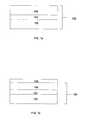
- a substrate 100may be a silicon on insulator (SOI) substrate.
- SOI substratetypically comprises an insulator layer sandwiched between two silicon layers.
- the substrate 100comprises a first silicon layer 102 , an insulator layer 104 disposed on the first silicon layer 102 , and a second silicon layer 106 disposed on the insulator layer 104 .
- the insulator layer 104may be an oxide, such as silicon dioxide.
- a dielectric layer 108may be formed on the second silicon layer 106 of the substrate 100 ( FIG. 1 b ).
- the dielectric layer 108may be formed using conventional techniques, such as plasma enhanced chemical vapor deposition (PECVD) or thermal oxidation techniques.
- PECVDplasma enhanced chemical vapor deposition
- the dielectric layer 108may then be patterned to form a silicon region 112 (by exposing the underlying second silicon layer 106 ), and at least one dielectric region (shown in FIG. 1 c as a first dielectric region 110 and a second dielectric region 110 ′).
- the dielectric layer 108may be patterned using standard lithographic techniques well known in the art, which typically comprise applying a photoresist on the dielectric layer 108 , exposing the photoresist in areas to be added (light mask) or removed (dark mask) and then performing the appropriate etch.
- a silicon germanium alloy layermay then be selectively formed over the silicon region 112 and the dielectric region 110 , 110 ′.
- Both a high defect silicon germanium layer 114 and at least one low defect silicon germanium layermay form during a single formation process step, to form a composite silicon germanium layer 118 which comprises the high defect silicon germanium layer 114 and the low defect silicon germanium layer 116 , 116 ′.
- the high defect silicon germanium layer 114 that forms over the silicon region 112comprises a defect density in the range of at least 10 6 defects per centimeter squared.
- defectsmay be in the form of threading dislocations that are formed to relieve the strain in the film lattice (due to a mismatch between the germanium and the silicon lattices) as it is being formed.
- the defects formed during the formation of the composite silicon germanium layer 118are substantially confined to the high defect silicon germanium layer 114 .
- the composite silicon germanium layer 118may be formed by selective epitaxy. In selective epitaxy, germanium is added to the silicon to form a silicon germanium alloy, such as the composite silicon germanium layer 118 .
- the composite silicon germanium layer 118 thus formedmay comprise at least 50 percent germanium, and preferably comprises greater than 50 percent germanium, and may further comprise 100 percent germanium.
- the composite silicon germanium layer 118may be formed by utilizing conventional methods, suitable for the deposition of silicon germanium films comprising greater than 50 percent germanium, such as by utilizing a chemical vapor deposition (CVD) or an epitaxial process, as are well known in the art.
- the deposition processmay include such process gases as SiH 2 Cl 2 and GeH 4 , or other suitable process gases.
- the process temperaturemay be in a range from about 600 to 750 degrees Celsius, but may vary depending on the process equipment and the particular application. It will be understood by those skilled in the art that while a few examples of the process parameters may be included herein, the composite silicon germanium layer 118 may be formed by other methods or processes that form a silicon germanium alloy comprising greater than 50 percent germanium.
- the low defect silicon germanium layer 116 , 116 ′ that forms over the dielectric region 110 , 110 ′may comprise a defect density below 10 6 defects per centimeter squared, and may preferably be virtually defect free, because the defects in the composite silicon germanium layer 118 are substantially confined to the high defect silicon germanium layer 114 .
- Selective epitaxy in the method of the present inventionmay also be called epitaxial lateral overgrowth (ELO) because the low defect silicon germanium layer 116 , 116 ′ forms laterally over at least one dielectric region (shown in FIG. 1 d as forming laterally over the first dielectric region 110 and the second dielectric region 110 ′).
- ELOepitaxial lateral overgrowth
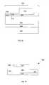
- a substrate 200which may be a SOI substrate (similar to the SOI substrate 100 in FIG. 1 a ), comprises first silicon layer 202 , an insulator layer 204 disposed on the first silicon layer 202 , and a second silicon layer 206 disposed on the insulator layer 204 ( FIG. 2 a ).
- the insulator layer 204may be an oxide, such as silicon dioxide.
- a buffer layer 207may be formed on the second silicon layer 206 of the substrate 200 ( FIG. 2 b ).
- the buffer layer 207may comprise silicon germanium, and may be formed by CVD epitaxy, or by any such methods used to form a silicon germanium alloy, such as the composite silicon germanium layer 118 as previously discussed herein.
- the buffer layer 207may be formed by using a grading technique, as is well known in the art, in which the buffer layer 207 is formed by sequentially increasing the percentage of germanium in the buffer layer 207 as the buffer layer 207 forms.
- the thickness of the buffer layer 207is preferably less than 1 micron thick.
- the buffer layer 207may also be formed by forming a thin layer of non-graded silicon germanium (preferably less than 1 micron in thickness), on the second silicon layer 206 .
- the buffer layer 207may then be cycled through an annealing process, as is known in the art. Defect concentrations of about 5 ⁇ 10 6 defects per centimeter squared may be obtained by using such a technique to form the buffer layer 207 .
- a dielectric layer 208may be formed on the buffer layer 207 ( FIG. 2 c ).
- the dielectric layer 208may then be patterned to form a buffer region 212 (by exposing the underlying buffer layer 207 ) and at least one dielectric region (shown in FIG. 2 d as a first dielectric region 210 and a second dielectric region 210 ′).
- a composite silicon germanium layer 218(similar to the composite silicon germanium layer 118 ) may then be formed ( FIG. 2 e ) on the buffer region 212 and the dielectric region 210 , 210 ′ by selective epitaxy, as previously described.
- the composite silicon germanium layer 218comprises at least 50 percent germanium.
- the composite silicon germanium alloy 218forms vertically over the buffer region 212 , and also forms laterally over the dielectric region 210 , 210 ′.
- the composite silicon germanium layer 218further comprises a high defect silicon germanium layer 214 (similar to high defect region 114 ) and at least one low defect silicon germanium layer (shown in FIG. 2 e as a first low defect silicon germanium layer 216 and a second low defect silicon germanium layer 216 ′, similar to low defect region 116 , 116 ′).
- the high defect silicon germanium layer 214 that forms over the buffer region 212may comprises a defect density in the range of about 5 ⁇ 10 6 defects per centimeter squared or lower, but the defect density of the high defect silicon germanium layer 214 is less than if the high defect silicon germanium layer 214 were grown directly on a silicon substrate, as in high defect layer 114 .
- the defects formed during the formation of the composite silicon germanium layer 218are substantially confined to the high defect silicon germanium layer 214 .
- the low defect silicon germanium layer 216 , 216 ′forms over the dielectric region 210 , 210 ′ by epitaxial lateral overgrowth.
- the defect density in the low defect silicon germanium layer 216 , 216 ′is below 10 6 defects per centimeter squared, and may be virtually defect free, because the defects in the composite silicon germanium layer 218 are substantially confined to the high defect silicon germanium layer 214 .
- the method of the present inventionprovides a high germanium concentration, low defect silicon germanium layer 216 , 216 ′ which incorporates a buffer layer 207 which reduces the defect density of the high defect silicon germanium layer 214 .
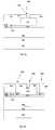
- a thin buffer buffer layer 507(similar to buffer layer 207 ) may be selectively formed over a silicon region 512 (similar to the silicon region 112 ).
- the silicon region 512 and a dielectric region 510 , 510 ′(similar to dielectric region 210 ′, 210 ′), are disposed on a substrate 500 ( FIG. 5 a ).
- the thin buffer layer 507is preferably less than 1 micron in thickness.
- a composite silicon germanium layer 518(similar to the composite silicon germanium layer 218 ) may then be formed over the silicon region 512 and the dielectric region 510 , 510 ′ ( FIG. 5 b ).
- the composite silicon germanium layer 518may comprises a high defect silicon germanium layer 514 (similar to the high defect silicon germanium, layer 214 ) and a low defect silicon germanium layer 516 , 516 ′ (similar to the low defect silicon germanium layer 216 , 216 ′).
- the current embodimentprovides a high germanium concentration, low defect silicon germanium layer 516 , 516 ′ which incorporates a thin buffer layer 507 which is selectively grown over the silicon region 512 .
- a substrate 300which may be a SOI substrate (similar to the SOI substrate 100 in FIG. 1 a ), comprises first silicon layer 302 , an insulator layer 304 disposed on the first silicon layer 302 , and a second silicon layer 306 disposed on the insulator layer 304 ( FIG. 3 a ).
- the insulator layer 304may be an oxide, such as silicon dioxide. It will be understood by those skilled in the art that the substrate 300 may include various structures, such as a trench structure, as is well known in the art.
- a dielectric layer 308may then be formed on the second silicon layer 306 of the silicon substrate 300 ( FIG. 3 b ) using conventional methods known in the art, such as CVD.
- the dielectric layer 308may then be patterned to form a silicon region 312 and at least one dielectric region (shown in FIG. 3 c as a first dielectric region 310 , and a second dielectric region 310 ′).
- a composite silicon germanium layer 318(similar to the composite silicon germanium layer 218 ) may then be formed ( FIG. 3 d ) by selective epitaxy, as previously described, wherein the composite silicon germanium layer 318 comprises at least 50 percent germanium.
- the composite silicon germanium layer 318forms vertically over the silicon region 312 and also forms laterally over the dielectric region 310 , 310 ′.
- the composite silicon germanium layer 318further comprises a high defect silicon germanium layer 314 and a low defect silicon germanium layer (shown in FIG. 3 d as a first low defect silicon germanium layer 316 , and a second low defect silicon germanium layer 316 ′).
- the high defect silicon germanium layer 314 that forms over the silicon region 312comprises a defect density in the range of about 5 ⁇ 10 6 defects per centimeter squared.
- the defects formed during the formation of the composite silicon germanium layer 318are substantially confined to the high defect silicon germanium layer 314 .
- the low defect silicon germanium layer 316 , 316forms over the dielectric region 310 , 310 ′ by epitaxial lateral overgrowth.
- the defect density in the low defect silicon germanium layer 316 , 316 ′is below 10 6 defects per centimeter squared, and may be virtually defect free, because the defects in the composite silicon germanium layer 318 are substantially confined to the high defect silicon germanium layer 314 .
- the composite silicon germanium layer 318may be patterned by methods known in the art to form a patterned composite silicon germanium structure 319 ( FIG. 3 e ). Such structures may include a waveguide, or other such optical devices used in optical communication systems, for example.
- the patterned composite silicon germanium structure 319may be further processed to form a p-i-n photodiode 320 (for ease of understanding, shown separated from the patterned composite silicon germanium structure 319 in FIG. 3 f ).
- the p-i-n photodiode 320may comprise at least one p-type low defect silicon germanium layer (shown in FIG.
- 3 fas a first p-type low defect silicon germanium layer 321 and a second p-type low defect silicon germanium layer 321 ′), an intrinsic low defect silicon germanium layer 322 , and an n-type low defect silicon germanium layer 323 .
- the p-i-n photodiode 320may be formed from the patterned composite silicon germanium structure 319 by first forming a mask 324 , as is well known in the art, on the patterned composite silicon germanium layer 319 ( FIG. 3 g ).
- the mask 324may comprise at least one implantation opening 325 to the low defect silicon germanium layer 316 .
- An ion implantation 326may be performed in which an n-type dopant (impurity) is implanted into an upper region 317 of the first low defect silicon germanium layer 316 .
- the n type dopantmay include such dopants as phosphorus, arsenic, or other such n-type dopant materials as are well known in the art.
- the upper region 317 of the first low defect silicon germanium layer 316which normally comprises an intrinsic level doping (i.e., there is no excess of either a p type or n-type dopant material) is doped with n-type dopant to form the n type low defect silicon germanium layer 323 of the p-i-n diode 320 (see FIG. 3 h ).
- the depth 328 of the upper region 317(as shown in FIG. 3 f ) may be adjusted according to the design parameters of the light sensing device 334 .
- the intrinsic low defect silicon germanium layer 322 of the p-i-n photodiode 320comprises the region of the first low defect silicon germanium layer 316 beneath the n type low defect silicon germanium layer 323 (which is normally intrinsic, as previously described, see FIG. 3 h ).
- the p-type low defect silicon germanium layer 321 , 321 ′is formed by first forming at least one metallization opening (illustrated in FIG. 3 h as a first metal mask opening 330 , a second metal mask opening 330 ′ and a third metal mask opening 330 ′′) in the mask 324 .
- a metal contactshown in FIG.
- the low defect silicon germanium contact region 327 , 327 ′is a region of the first low defect silicon germanium layer 316 that is not beneath the n type low defect silicon germanium layer 323 .
- the first metal contact 332 and the third metal contact 332 ′′ that form on the first low defect silicon germanium contact region 327 and the second low defect silicon germanium contact region 327 ′ respectively,may dope the low defect silicon germanium contact region 327 , 327 ′ with a p-type dopant.
- the metal contact 332 , 332 ′′′is aluminum
- the aluminum metalitself may provide a p-type dopant to the low defect silicon germanium contact region 327 , 327 ′, thus forming the p-type low defect silicon germanium layer 321 , 321 ′ of the p-i-n diode 320 ( FIG. 3 i ).
- the second metal contact 332 ′may also form on the n type low defect silicon germanium layer 323 during the same process step which forms the first metal contact 332 and the third metal contact 332 ′′.
- Metallization to the photodiode 320is thus enabled and in this manner the light sensing device 334 , which form a portion of an optical device, such as a waveguide, as is well known in the art may be formed.
- the doping of the p-i-n photodiode 320 of the light sensing device 334may be performed by using other techniques known in the art with which to dope the n and p type layers of such photodiodes, such as the n type low defect silicon germanium layer 323 and the p type low defect silicon germanium layer 321 , 321 ′.
- Such techniquesmay include (by example and not limitation) using a CVD deposition, or other non-implant techniques of doping a silicon germanium film as are known in the art.
- the light sensing device 334may include other types of photodiodes, such as a metal semiconductor metal (MSM) diode, as is well known in the art (and thus will not be described further herein), and is not limited to a p-i-n photodiode.
- MSMmetal semiconductor metal
- FIG. 4is a diagram illustrating one embodiment of an optical communication system 400 including an optical device 404 , such as the light sensing device 334 of the present invention.
- the optical device 404may include a light sensing device, such as a waveguide.
- the optical communication system 400includes an optical transmitter 402 to transmit an optical beam 408 .
- An optical receiver 406is optically coupled to receive the optical beam 408 .
- the optical transmitter 402 and the optical receiver 406may also include optical transceivers and therefore have both transmitting and receiving capabilities for bi-directional communications.
- the optical device 404is optically coupled between optical transmitter 402 and optical receiver 406 .
- optical device 404is shown to be at the receiving end of optical communication system 400 .
- the optical device 404may be disposed at various locations along a transmission path or at the transmitting end of the optical communication system 400 .
- the optical device 404may be included in a waveguide and be utilized in for example an add/drop filter, as is well known in the art, that enables the addition or extraction of a channel from a wave division multiplexed (WDM, also well known in the art) optical beam 408 transmitted from optical transmitter 402 along an optical path.
- WDMwave division multiplexed
- an optical beam 410 having a specific wavelengthis output from the optical device 404 .
- the present inventionprovides methods and associated structures of forming a high germanium concentration, low defect density silicon germanium film in order to enable microelectronic devices which are capable of operating at wavelengths of 1.3 microns and above.
- the dark current of a devicemay be to about 10 microamperes or below. This greatly enhances the reliability and performance of a device fabricated according to the various embodiments of the present invention.
Landscapes
- Engineering & Computer Science (AREA)
- Physics & Mathematics (AREA)
- Condensed Matter Physics & Semiconductors (AREA)
- General Physics & Mathematics (AREA)
- Manufacturing & Machinery (AREA)
- Computer Hardware Design (AREA)
- Microelectronics & Electronic Packaging (AREA)
- Power Engineering (AREA)
- Chemical & Material Sciences (AREA)
- Materials Engineering (AREA)
- Crystallography & Structural Chemistry (AREA)
- Light Receiving Elements (AREA)
Abstract
Description
- The present invention relates to the field of semiconductor processing, and more particularly to methods of processing germanium layers for use in microelectronic photo detectors and structures formed thereby.
- High speed infrared photodetectors are becoming increasingly important for optical communication signal processing, infrared imaging and measurement systems. Photodetectors can be used for the detection of optical communication signals, such as those used in the telecommunication industry. A standard wavelength used in the telecommunication industry is 1.3 microns. Pure silicon photodetectors are limited in that they can only detect wavelengths up to about 1 micron. The addition of germanium to a silicon film used to fabricate a photodetector can increase the wavelength that can be detected (i.e., photodetector responsivity). For example, using a silicon-germanium film which incorporates more than 50 percent germanium can increase the photodetector responsivity to 1.3 microns or more. However, adding germanium to the silicon film often results in a strain to the silicon crystal lattice that may causes defects, such as threading dislocations, to be formed in the silicon-germanium film. The proliferation of such defects can result in an increase in the defect concentration, or defect density, in the silicon germanium film, which can impair the performance of a silicon germanium photodetector device.
- Accordingly, there is a need for improved methods of forming a silicon germanium film and structures formed thereby which incorporate greater than 50 percent germanium concentration while exhibiting low defect concentrations. The present invention provides such methods and structures.
- While the specification concludes with claims particularly pointing out and distinctly claiming that which is regarded as the present invention, the advantages of this invention can be more readily ascertained from the following description of the invention when read in conjunction with the accompanying drawings in which:
FIGS. 1 a-1drepresent cross-sections of structures that may be formed when carrying out an embodiment of the method of the present invention.FIGS. 2 a-2erepresent cross-sections of structures that may be formed when carrying out another embodiment of the method of the present invention.FIGS. 3 a-3irepresent cross-sections of structures that may be formed when carrying out another embodiment of the method of the present invention.FIG. 4 represents an embodiment of an optical system in accordance with the methods of the present invention.FIGS. 5 a-5brepresent cross-sections of structures that may be formed when carrying out another embodiment of the method of the present invention.- In the following detailed description, reference is made to the accompanying drawings that show, by way of illustration, specific embodiments in which the invention may be practiced. These embodiments are described in sufficient detail to enable those skilled in the art to practice the invention. It is to be understood that the various embodiments of the invention, although different, are not necessarily mutually exclusive. For example, a particular feature, structure, or characteristic described herein, in connection with one embodiment, may be implemented within other embodiments without departing from the spirit and scope of the invention. In addition, it is to be understood that the location or arrangement of individual elements within each disclosed embodiment may be modified without departing from the spirit and scope of the invention. The following detailed description is, therefore, not to be taken in a limiting sense, and the scope of the present invention is defined only by the appended claims, appropriately interpreted, along with the full range of equivalents to which the claims are entitled. In the drawings, like numerals refer to the same or similar functionality throughout the several views.
- Methods of forming a high germanium concentration, low defect density silicon germanium film and its associated structures are described. The methods and associated structures of the present invention confine the defect density of the silicon germanium film in a non-active device area, while providing for a low defect density silicon germanium film in an active area of the device. The formation of a such a low defect silicon germanium film comprises forming a dielectric layer on a substrate, patterning the dielectric layer to form a silicon region and at least one dielectric region, and forming a silicon germanium layer on at least one dielectric region and on the silicon region, wherein the silicon germanium layer formed on the dielectric region has a low defect concentration i.e., less than about 106defects per cm2. The high germanium concentration, low defect density layer may then be used to form a microelectronic device, such as a photodetector, and thus enables the use of a silicon germanium based microelectronic photodetector which operates at a wavelength of at least 1.3 microns.
- In one embodiment of the method of the present invention, as illustrated by
FIGS. 1 a-1d,asubstrate 100 may be a silicon on insulator (SOI) substrate. A SOI substrate typically comprises an insulator layer sandwiched between two silicon layers. As shown inFIG. 1 a,thesubstrate 100 comprises afirst silicon layer 102, aninsulator layer 104 disposed on thefirst silicon layer 102, and asecond silicon layer 106 disposed on theinsulator layer 104. Theinsulator layer 104 may be an oxide, such as silicon dioxide. - A
dielectric layer 108 may be formed on thesecond silicon layer 106 of the substrate100 (FIG. 1 b). Those skilled in the art will appreciate that thedielectric layer 108 may be formed using conventional techniques, such as plasma enhanced chemical vapor deposition (PECVD) or thermal oxidation techniques. Thedielectric layer 108 may then be patterned to form a silicon region112 (by exposing the underlying second silicon layer106), and at least one dielectric region (shown inFIG. 1 cas a firstdielectric region 110 and a seconddielectric region 110′). Thedielectric layer 108 may be patterned using standard lithographic techniques well known in the art, which typically comprise applying a photoresist on thedielectric layer 108, exposing the photoresist in areas to be added (light mask) or removed (dark mask) and then performing the appropriate etch. - A silicon germanium alloy layer may then be selectively formed over the
silicon region 112 and thedielectric region silicon germanium layer 114 and at least one low defect silicon germanium layer (shown inFIG. 1 das a first low defectsilicon germanium layer 116 and a second low defectsilicon germanium layer 116′) may form during a single formation process step, to form a compositesilicon germanium layer 118 which comprises the high defectsilicon germanium layer 114 and the low defectsilicon germanium layer silicon germanium layer 114 that forms over thesilicon region 112 comprises a defect density in the range of at least 106defects per centimeter squared. These defects may be in the form of threading dislocations that are formed to relieve the strain in the film lattice (due to a mismatch between the germanium and the silicon lattices) as it is being formed. The defects formed during the formation of the compositesilicon germanium layer 118 are substantially confined to the high defectsilicon germanium layer 114. - The composite
silicon germanium layer 118 may be formed by selective epitaxy. In selective epitaxy, germanium is added to the silicon to form a silicon germanium alloy, such as the compositesilicon germanium layer 118. The compositesilicon germanium layer 118 thus formed may comprise at least 50 percent germanium, and preferably comprises greater than 50 percent germanium, and may further comprise 100 percent germanium. The compositesilicon germanium layer 118 may be formed by utilizing conventional methods, suitable for the deposition of silicon germanium films comprising greater than 50 percent germanium, such as by utilizing a chemical vapor deposition (CVD) or an epitaxial process, as are well known in the art. The deposition process may include such process gases as SiH2Cl2and GeH4, or other suitable process gases. The process temperature may be in a range from about 600 to 750 degrees Celsius, but may vary depending on the process equipment and the particular application. It will be understood by those skilled in the art that while a few examples of the process parameters may be included herein, the compositesilicon germanium layer 118 may be formed by other methods or processes that form a silicon germanium alloy comprising greater than 50 percent germanium. - The low defect
silicon germanium layer dielectric region silicon germanium layer 118 are substantially confined to the high defectsilicon germanium layer 114. Selective epitaxy in the method of the present invention may also be called epitaxial lateral overgrowth (ELO) because the low defectsilicon germanium layer FIG. 1 das forming laterally over the firstdielectric region 110 and the seconddielectric region 110′). Thus, the method of the present invention provides a high germanium concentration, low defectsilicon germanium layer - In another embodiment of the present invention (
FIGS. 2 a-2e), asubstrate 200, which may be a SOI substrate (similar to theSOI substrate 100 inFIG. 1 a), comprisesfirst silicon layer 202, aninsulator layer 204 disposed on thefirst silicon layer 202, and asecond silicon layer 206 disposed on the insulator layer204 (FIG. 2 a). Theinsulator layer 204 may be an oxide, such as silicon dioxide. - A
buffer layer 207 may be formed on thesecond silicon layer 206 of the substrate200 (FIG. 2 b). Thebuffer layer 207 may comprise silicon germanium, and may be formed by CVD epitaxy, or by any such methods used to form a silicon germanium alloy, such as the compositesilicon germanium layer 118 as previously discussed herein. Thebuffer layer 207 may be formed by using a grading technique, as is well known in the art, in which thebuffer layer 207 is formed by sequentially increasing the percentage of germanium in thebuffer layer 207 as thebuffer layer 207 forms. The thickness of thebuffer layer 207 is preferably less than 1 micron thick. Thebuffer layer 207 may also be formed by forming a thin layer of non-graded silicon germanium (preferably less than 1 micron in thickness), on thesecond silicon layer 206. Thebuffer layer 207 may then be cycled through an annealing process, as is known in the art. Defect concentrations of about 5×10⁶defects per centimeter squared may be obtained by using such a technique to form thebuffer layer 207. - A
dielectric layer 208 may be formed on the buffer layer207 (FIG. 2 c). Thedielectric layer 208 may then be patterned to form a buffer region212 (by exposing the underlying buffer layer207) and at least one dielectric region (shown inFIG. 2 das a firstdielectric region 210 and a seconddielectric region 210′). A composite silicon germanium layer218 (similar to the composite silicon germanium layer118) may then be formed (FIG. 2 e) on thebuffer region 212 and thedielectric region silicon germanium layer 218 comprises at least 50 percent germanium. The compositesilicon germanium alloy 218 forms vertically over thebuffer region 212, and also forms laterally over thedielectric region silicon germanium layer 218 further comprises a high defect silicon germanium layer214 (similar to high defect region114) and at least one low defect silicon germanium layer (shown inFIG. 2 eas a first low defectsilicon germanium layer 216 and a second low defectsilicon germanium layer 216′, similar tolow defect region silicon germanium layer 214 that forms over thebuffer region 212 may comprises a defect density in the range of about 5×10⁶defects per centimeter squared or lower, but the defect density of the high defectsilicon germanium layer 214 is less than if the high defectsilicon germanium layer 214 were grown directly on a silicon substrate, as inhigh defect layer 114. The defects formed during the formation of the compositesilicon germanium layer 218 are substantially confined to the high defectsilicon germanium layer 214. - The low defect
silicon germanium layer dielectric region silicon germanium layer silicon germanium layer 218 are substantially confined to the high defectsilicon germanium layer 214. Thus, the method of the present invention provides a high germanium concentration, low defectsilicon germanium layer buffer layer 207 which reduces the defect density of the high defectsilicon germanium layer 214. - In another embodiment (
FIG. 5 a), a thin buffer buffer layer507 (similar to buffer layer207) may be selectively formed over a silicon region512 (similar to the silicon region112). Thesilicon region 512 and adielectric region dielectric region 210′,210′), are disposed on a substrate500 (FIG. 5 a). Thethin buffer layer 507 is preferably less than 1 micron in thickness. A composite silicon germanium layer518 (similar to the composite silicon germanium layer218) may then be formed over thesilicon region 512 and thedielectric region FIG. 5 b). The compositesilicon germanium layer 518 may comprises a high defect silicon germanium layer514 (similar to the high defect silicon germanium, layer214) and a low defectsilicon germanium layer silicon germanium layer silicon germanium layer thin buffer layer 507 which is selectively grown over thesilicon region 512. - In another embodiment of the present invention, a method of forming a microelectronic device, such as a light-sensing device334 (
FIG. 3 i) and structures formed thereby is illustrated inFIGS. 3 a-3i.Asubstrate 300, which may be a SOI substrate (similar to theSOI substrate 100 inFIG. 1 a), comprisesfirst silicon layer 302, aninsulator layer 304 disposed on thefirst silicon layer 302, and asecond silicon layer 306 disposed on the insulator layer304 (FIG. 3 a). Theinsulator layer 304 may be an oxide, such as silicon dioxide. It will be understood by those skilled in the art that thesubstrate 300 may include various structures, such as a trench structure, as is well known in the art. - A
dielectric layer 308 may then be formed on thesecond silicon layer 306 of the silicon substrate300 (FIG. 3 b) using conventional methods known in the art, such as CVD. Thedielectric layer 308 may then be patterned to form asilicon region 312 and at least one dielectric region (shown inFIG. 3 cas a firstdielectric region 310, and a seconddielectric region 310′). - A composite silicon germanium layer318 (similar to the composite silicon germanium layer218) may then be formed (
FIG. 3 d) by selective epitaxy, as previously described, wherein the compositesilicon germanium layer 318 comprises at least 50 percent germanium. The compositesilicon germanium layer 318 forms vertically over thesilicon region 312 and also forms laterally over thedielectric region silicon germanium layer 318 further comprises a high defectsilicon germanium layer 314 and a low defect silicon germanium layer (shown inFIG. 3 das a first low defectsilicon germanium layer 316, and a second low defectsilicon germanium layer 316′). The high defectsilicon germanium layer 314 that forms over thesilicon region 312 comprises a defect density in the range of about 5×10⁶defects per centimeter squared. The defects formed during the formation of the compositesilicon germanium layer 318 are substantially confined to the high defectsilicon germanium layer 314. - The low defect
silicon germanium layer dielectric region silicon germanium layer silicon germanium layer 318 are substantially confined to the high defectsilicon germanium layer 314. - The composite
silicon germanium layer 318 may be patterned by methods known in the art to form a patterned composite silicon germanium structure319 (FIG. 3 e). Such structures may include a waveguide, or other such optical devices used in optical communication systems, for example. The patterned compositesilicon germanium structure 319 may be further processed to form a p-i-n photodiode320 (for ease of understanding, shown separated from the patterned compositesilicon germanium structure 319 inFIG. 3 f). Thep-i-n photodiode 320 may comprise at least one p-type low defect silicon germanium layer (shown in FIG.3fas a first p-type low defectsilicon germanium layer 321 and a second p-type low defectsilicon germanium layer 321′), an intrinsic low defectsilicon germanium layer 322, and an n-type low defectsilicon germanium layer 323. - The
p-i-n photodiode 320 may be formed from the patterned compositesilicon germanium structure 319 by first forming amask 324, as is well known in the art, on the patterned composite silicon germanium layer319 (FIG. 3 g). Themask 324 may comprise at least oneimplantation opening 325 to the low defectsilicon germanium layer 316. Anion implantation 326, as is well known in the art, may be performed in which an n-type dopant (impurity) is implanted into anupper region 317 of the first low defectsilicon germanium layer 316. The n type dopant may include such dopants as phosphorus, arsenic, or other such n-type dopant materials as are well known in the art. In this manner, theupper region 317 of the first low defectsilicon germanium layer 316, which normally comprises an intrinsic level doping (i.e., there is no excess of either a p type or n-type dopant material) is doped with n-type dopant to form the n type low defectsilicon germanium layer 323 of the p-i-n diode320 (seeFIG. 3 h). Thedepth 328 of the upper region317 (as shown inFIG. 3 f) may be adjusted according to the design parameters of thelight sensing device 334. - The intrinsic low defect
silicon germanium layer 322 of thep-i-n photodiode 320 comprises the region of the first low defectsilicon germanium layer 316 beneath the n type low defect silicon germanium layer323 (which is normally intrinsic, as previously described, seeFIG. 3 h). The p-type low defectsilicon germanium layer FIG. 3 has a firstmetal mask opening 330, a second metal mask opening330′ and a thirdmetal mask opening 330″) in themask 324. A metal contact (shown inFIG. 3 ias afirst metal contact 332, asecond metal contact 332′ and athird metal contact 332″) may then be formed on at least one low defect silicon germanium contact region (shown inFIG. 3 has a first low defect silicongermanium contact region 327 and a second low defect silicongermanium contact region 327′) in a manner well known in the art. The low defect silicongermanium contact region silicon germanium layer 316 that is not beneath the n type low defectsilicon germanium layer 323. Thefirst metal contact 332 and thethird metal contact 332″ that form on the first low defect silicongermanium contact region 327 and the second low defect silicongermanium contact region 327′ respectively, may dope the low defect silicongermanium contact region metal contact germanium contact region silicon germanium layer FIG. 3 i). Thesecond metal contact 332′ may also form on the n type low defectsilicon germanium layer 323 during the same process step which forms thefirst metal contact 332 and thethird metal contact 332″. Metallization to thephotodiode 320 is thus enabled and in this manner thelight sensing device 334, which form a portion of an optical device, such as a waveguide, as is well known in the art may be formed. - It will be appreciated by those skilled in the art that the doping of the
p-i-n photodiode 320 of thelight sensing device 334 may be performed by using other techniques known in the art with which to dope the n and p type layers of such photodiodes, such as the n type low defectsilicon germanium layer 323 and the p type low defectsilicon germanium layer light sensing device 334 may include other types of photodiodes, such as a metal semiconductor metal (MSM) diode, as is well known in the art (and thus will not be described further herein), and is not limited to a p-i-n photodiode. - The
light sensing device 334 formed according to the method of the current embodiment may be used in any number of optical communication systems. For example, it is capable of being used in the telecommunications industry, since it is capable of operating above 1.3 microns, which is the telecommunications industry standard operating wavelength.FIG. 4 is a diagram illustrating one embodiment of anoptical communication system 400 including anoptical device 404, such as thelight sensing device 334 of the present invention. In various embodiments theoptical device 404 may include a light sensing device, such as a waveguide. In the depicted embodiment, theoptical communication system 400 includes anoptical transmitter 402 to transmit anoptical beam 408. Anoptical receiver 406 is optically coupled to receive theoptical beam 408. It is appreciated that theoptical transmitter 402 and theoptical receiver 406 may also include optical transceivers and therefore have both transmitting and receiving capabilities for bi-directional communications. In one embodiment, theoptical device 404 is optically coupled betweenoptical transmitter 402 andoptical receiver 406. In the illustrated embodiment,optical device 404 is shown to be at the receiving end ofoptical communication system 400. In other embodiments, theoptical device 404 may be disposed at various locations along a transmission path or at the transmitting end of theoptical communication system 400. In one embodiment, theoptical device 404 may be included in a waveguide and be utilized in for example an add/drop filter, as is well known in the art, that enables the addition or extraction of a channel from a wave division multiplexed (WDM, also well known in the art)optical beam 408 transmitted fromoptical transmitter 402 along an optical path. Thus, anoptical beam 410 having a specific wavelength is output from theoptical device 404. - As described above, the present invention provides methods and associated structures of forming a high germanium concentration, low defect density silicon germanium film in order to enable microelectronic devices which are capable of operating at wavelengths of 1.3 microns and above. In addition, because there are less defects per centimeter squared in the low defect silicon germanium layer of the present invention, the dark current of a device (a measurement of current leakage during non-operating times), may be to about 10 microamperes or below. This greatly enhances the reliability and performance of a device fabricated according to the various embodiments of the present invention.
- Although the foregoing description has specified certain steps and materials that may be used in the method of the present invention, those skilled in the art will appreciate that many modifications and substitutions may be made. Accordingly, it is intended that all such modifications, alterations, substitutions and additions be considered to fall within the spirit and scope of the invention as defined by the appended claims. In addition, it is appreciated that the fabrication of a multiple metal layer structure atop a substrate, such as a silicon substrate, to manufacture a silicon device is well known in the art. Therefore, it is appreciated that the Figures provided herein illustrate only portions of an exemplary microelectronic device that pertains to the practice of the present invention. Thus the present invention is not limited to the structures described herein.
Claims (14)
1.-11. (canceled)
12. A microelectronic structure, comprising:
a dielectric layer disposed on a substrate; and
a low defect silicon germanium layer disposed on the dielectric layer.
13. The structure ofclaim 12 wherein the low defect silicon germanium layer comprises greater than 50% germanium.
14. The structure ofclaim 12 wherein the low defect silicon germanium layer is formed by ELO.
15. The structure ofclaim 12 wherein the low defect silicon germanium layer comprises less than about 106defects per cm2.
16. The structure ofclaim 12 wherein the substrate comprises a silicon on insulator (SOI) substrate.
17. A photodiode comprising:
an n-doped low defect silicon germanium layer disposed on a dielectric region; and
a p-doped low defect silicon germanium layer disposed on a silicon region;
18. The photodiode ofclaim 17 wherein the photodiode is capable of detecting a wavelength greater than 1.3 microns.
19. The photodiode ofclaim 17 wherein the photodiode comprises a p-i-n diode.
20. The photodiode ofclaim 17 wherein the photodiode comprises a metal semiconductor metal (MSM) diode.
21. The photodiode ofclaim 17 wherein the low defect silicon germanium layer comprise less than about 106defects per cm2.
22. The photodiode ofclaim 17 wherein the low defect silicon germanium layer comprises at least 50 percent germanium.
23. The photodiode ofclaim 17 wherein the dark current is less than 10 microamperes.
24.-28. (canceled)
Priority Applications (1)
| Application Number | Priority Date | Filing Date | Title |
|---|---|---|---|
| US11/035,628US7180147B2 (en) | 2003-06-30 | 2005-01-12 | Microelectronic structure with a high germanium concentration silicon germanium alloy including a graded buffer layer |
Applications Claiming Priority (2)
| Application Number | Priority Date | Filing Date | Title |
|---|---|---|---|
| US10/611,042US7122392B2 (en) | 2003-06-30 | 2003-06-30 | Methods of forming a high germanium concentration silicon germanium alloy by epitaxial lateral overgrowth and structures formed thereby |
| US11/035,628US7180147B2 (en) | 2003-06-30 | 2005-01-12 | Microelectronic structure with a high germanium concentration silicon germanium alloy including a graded buffer layer |
Related Parent Applications (1)
| Application Number | Title | Priority Date | Filing Date |
|---|---|---|---|
| US10/611,042DivisionUS7122392B2 (en) | 2003-06-30 | 2003-06-30 | Methods of forming a high germanium concentration silicon germanium alloy by epitaxial lateral overgrowth and structures formed thereby |
Publications (2)
| Publication Number | Publication Date |
|---|---|
| US20050136626A1true US20050136626A1 (en) | 2005-06-23 |
| US7180147B2 US7180147B2 (en) | 2007-02-20 |
Family
ID=33541239
Family Applications (3)
| Application Number | Title | Priority Date | Filing Date |
|---|---|---|---|
| US10/611,042Expired - Fee RelatedUS7122392B2 (en) | 2003-06-30 | 2003-06-30 | Methods of forming a high germanium concentration silicon germanium alloy by epitaxial lateral overgrowth and structures formed thereby |
| US11/035,921Expired - Fee RelatedUS7180148B2 (en) | 2003-06-30 | 2005-01-12 | Optical system with a high germanium concentration silicon germanium alloy including a graded buffer layer |
| US11/035,628Expired - Fee RelatedUS7180147B2 (en) | 2003-06-30 | 2005-01-12 | Microelectronic structure with a high germanium concentration silicon germanium alloy including a graded buffer layer |
Family Applications Before (2)
| Application Number | Title | Priority Date | Filing Date |
|---|---|---|---|
| US10/611,042Expired - Fee RelatedUS7122392B2 (en) | 2003-06-30 | 2003-06-30 | Methods of forming a high germanium concentration silicon germanium alloy by epitaxial lateral overgrowth and structures formed thereby |
| US11/035,921Expired - Fee RelatedUS7180148B2 (en) | 2003-06-30 | 2005-01-12 | Optical system with a high germanium concentration silicon germanium alloy including a graded buffer layer |
Country Status (1)
| Country | Link |
|---|---|
| US (3) | US7122392B2 (en) |
Cited By (23)
| Publication number | Priority date | Publication date | Assignee | Title |
|---|---|---|---|---|
| US20050054180A1 (en)* | 2003-09-09 | 2005-03-10 | Sang Han | Threading-dislocation-free nanoheteroepitaxy of Ge on Si using self-directed touch-down of Ge through a thin SiO2 layer |
| US20100295083A1 (en)* | 2008-03-19 | 2010-11-25 | Celler George K | Substrates for monolithic optical circuits and electronic circuits |
| CN102034833A (en)* | 2009-09-24 | 2011-04-27 | 台湾积体电路制造股份有限公司 | Sensor and its manufacturing method |
| KR20120011117A (en)* | 2010-07-28 | 2012-02-07 | 삼성전자주식회사 | Method for forming photodetector structure |
| US8216951B2 (en) | 2006-09-27 | 2012-07-10 | Taiwan Semiconductor Manufacturing Company, Ltd. | Quantum tunneling devices and circuits with lattice-mismatched semiconductor structures |
| US8237151B2 (en) | 2009-01-09 | 2012-08-07 | Taiwan Semiconductor Manufacturing Company, Ltd. | Diode-based devices and methods for making the same |
| US8253211B2 (en)* | 2008-09-24 | 2012-08-28 | Taiwan Semiconductor Manufacturing Company, Ltd. | Semiconductor sensor structures with reduced dislocation defect densities |
| US8274097B2 (en) | 2008-07-01 | 2012-09-25 | Taiwan Semiconductor Manufacturing Company, Ltd. | Reduction of edge effects from aspect ratio trapping |
| US8304805B2 (en) | 2009-01-09 | 2012-11-06 | Taiwan Semiconductor Manufacturing Company, Ltd. | Semiconductor diodes fabricated by aspect ratio trapping with coalesced films |
| US8324660B2 (en) | 2005-05-17 | 2012-12-04 | Taiwan Semiconductor Manufacturing Company, Ltd. | Lattice-mismatched semiconductor structures with reduced dislocation defect densities and related methods for device fabrication |
| US8329541B2 (en) | 2007-06-15 | 2012-12-11 | Taiwan Semiconductor Manufacturing Company, Ltd. | InP-based transistor fabrication |
| US8344242B2 (en) | 2007-09-07 | 2013-01-01 | Taiwan Semiconductor Manufacturing Company, Ltd. | Multi-junction solar cells |
| US8384196B2 (en) | 2008-09-19 | 2013-02-26 | Taiwan Semiconductor Manufacturing Company, Ltd. | Formation of devices by epitaxial layer overgrowth |
| US8502263B2 (en) | 2006-10-19 | 2013-08-06 | Taiwan Semiconductor Manufacturing Company, Ltd. | Light-emitter-based devices with lattice-mismatched semiconductor structures |
| US8624103B2 (en) | 2007-04-09 | 2014-01-07 | Taiwan Semiconductor Manufacturing Company, Ltd. | Nitride-based multi-junction solar cell modules and methods for making the same |
| US8629446B2 (en) | 2009-04-02 | 2014-01-14 | Taiwan Semiconductor Manufacturing Company, Ltd. | Devices formed from a non-polar plane of a crystalline material and method of making the same |
| US8822248B2 (en) | 2008-06-03 | 2014-09-02 | Taiwan Semiconductor Manufacturing Company, Ltd. | Epitaxial growth of crystalline material |
| US8847279B2 (en) | 2006-09-07 | 2014-09-30 | Taiwan Semiconductor Manufacturing Company, Ltd. | Defect reduction using aspect ratio trapping |
| US8878243B2 (en) | 2006-03-24 | 2014-11-04 | Taiwan Semiconductor Manufacturing Company, Ltd. | Lattice-mismatched semiconductor structures and related methods for device fabrication |
| US8981427B2 (en) | 2008-07-15 | 2015-03-17 | Taiwan Semiconductor Manufacturing Company, Ltd. | Polishing of small composite semiconductor materials |
| US9508890B2 (en) | 2007-04-09 | 2016-11-29 | Taiwan Semiconductor Manufacturing Company, Ltd. | Photovoltaics on silicon |
| US9859381B2 (en) | 2005-05-17 | 2018-01-02 | Taiwan Semiconductor Manufacturing Company, Ltd. | Lattice-mismatched semiconductor structures with reduced dislocation defect densities and related methods for device fabrication |
| US9984872B2 (en) | 2008-09-19 | 2018-05-29 | Taiwan Semiconductor Manufacturing Company, Ltd. | Fabrication and structures of crystalline material |
Families Citing this family (41)
| Publication number | Priority date | Publication date | Assignee | Title |
|---|---|---|---|---|
| US20050257532A1 (en)* | 2004-03-11 | 2005-11-24 | Masami Ikeda | Module for cooling semiconductor device |
| US20060073681A1 (en)* | 2004-09-08 | 2006-04-06 | Han Sang M | Nanoheteroepitaxy of Ge on Si as a foundation for group III-V and II-VI integration |
| KR100634444B1 (en)* | 2004-12-20 | 2006-10-16 | 삼성전자주식회사 | Light receiving element and its formation method |
| US20060157806A1 (en)* | 2005-01-18 | 2006-07-20 | Omnivision Technologies, Inc. | Multilayered semiconductor susbtrate and image sensor formed thereon for improved infrared response |
| WO2007027615A1 (en)* | 2005-09-01 | 2007-03-08 | Applied Materials, Inc. | Ridge technique for fabricating an optical detector and an optical waveguide |
| FR2896338B1 (en) | 2006-01-17 | 2008-04-18 | St Microelectronics Crolles 2 | METHOD FOR MAKING A MONOCRYSTALLINE LAYER ON A DIELECTRIC LAYER |
| FR2896337A1 (en)* | 2006-01-17 | 2007-07-20 | St Microelectronics Crolles 2 | METHOD FOR MAKING A MONOCRYSTALLINE LAYER ON A DIELECTRIC LAYER |
| US7553687B2 (en)* | 2006-06-28 | 2009-06-30 | Intel Corporation | Dual seed semiconductor photodetectors |
| TWI328884B (en)* | 2007-05-14 | 2010-08-11 | Au Optronics Corp | Photo detector and method for forming thereof |
| US20100071765A1 (en)* | 2008-09-19 | 2010-03-25 | Peter Cousins | Method for fabricating a solar cell using a direct-pattern pin-hole-free masking layer |
| JP5583943B2 (en)* | 2008-10-02 | 2014-09-03 | 住友化学株式会社 | Semiconductor substrate, electronic device, and method for manufacturing semiconductor substrate |
| US8115095B2 (en)* | 2009-02-20 | 2012-02-14 | Miasole | Protective layer for large-scale production of thin-film solar cells |
| US8110738B2 (en) | 2009-02-20 | 2012-02-07 | Miasole | Protective layer for large-scale production of thin-film solar cells |
| US7897020B2 (en)* | 2009-04-13 | 2011-03-01 | Miasole | Method for alkali doping of thin film photovoltaic materials |
| US8134069B2 (en)* | 2009-04-13 | 2012-03-13 | Miasole | Method and apparatus for controllable sodium delivery for thin film photovoltaic materials |
| US7785921B1 (en) | 2009-04-13 | 2010-08-31 | Miasole | Barrier for doped molybdenum targets |
| US9284639B2 (en)* | 2009-07-30 | 2016-03-15 | Apollo Precision Kunming Yuanhong Limited | Method for alkali doping of thin film photovoltaic materials |
| US7871854B1 (en) | 2009-08-19 | 2011-01-18 | Freescale Semiconductor, Inc. | Method of making a vertical photodetector |
| US8709548B1 (en) | 2009-10-20 | 2014-04-29 | Hanergy Holding Group Ltd. | Method of making a CIG target by spray forming |
| US8709335B1 (en) | 2009-10-20 | 2014-04-29 | Hanergy Holding Group Ltd. | Method of making a CIG target by cold spraying |
| US20110162696A1 (en)* | 2010-01-05 | 2011-07-07 | Miasole | Photovoltaic materials with controllable zinc and sodium content and method of making thereof |
| US8048707B1 (en) | 2010-10-19 | 2011-11-01 | Miasole | Sulfur salt containing CIG targets, methods of making and methods of use thereof |
| US7935558B1 (en) | 2010-10-19 | 2011-05-03 | Miasole | Sodium salt containing CIG targets, methods of making and methods of use thereof |
| US9169548B1 (en) | 2010-10-19 | 2015-10-27 | Apollo Precision Fujian Limited | Photovoltaic cell with copper poor CIGS absorber layer and method of making thereof |
| CN102456541B (en)* | 2010-10-19 | 2013-07-24 | 上海华虹Nec电子有限公司 | Preparation method of SiGe monitoring piece and method for employing piece to carry out monitoring |
| US10043921B1 (en) | 2011-12-21 | 2018-08-07 | Beijing Apollo Ding Rong Solar Technology Co., Ltd. | Photovoltaic cell with high efficiency cigs absorber layer with low minority carrier lifetime and method of making thereof |
| US9153717B2 (en)* | 2013-08-09 | 2015-10-06 | Taiwan Semiconductor Manufacturing Company, Ltd. | Backside illuminated photo-sensitive device with gradated buffer layer |
| US10928659B2 (en) | 2014-02-24 | 2021-02-23 | Rockley Photonics Limited | Optoelectronic device |
| US10222677B2 (en) | 2014-02-24 | 2019-03-05 | Rockley Photonics Limited | Optoelectronic device |
| US10216059B2 (en) | 2015-03-05 | 2019-02-26 | Rockley Photonics Limited | Waveguide modulator structures |
| US10921616B2 (en) | 2016-11-23 | 2021-02-16 | Rockley Photonics Limited | Optoelectronic device |
| GB2552618B (en) | 2015-03-05 | 2021-07-28 | Rockley Photonics Ltd | Waveguide modulator structures |
| US10678115B2 (en) | 2015-03-05 | 2020-06-09 | Rockley Photonics Limited | Waveguide modulator structures |
| US11150494B2 (en) | 2015-03-05 | 2021-10-19 | Rockley Photonics Limited | Waveguide modulator structures |
| US9530669B1 (en)* | 2015-11-30 | 2016-12-27 | International Business Machines Corporation | Method of making a semiconductor device having a semiconductor material on a relaxed semiconductor including replacing a strained, selective etchable material, with a low density dielectric in a cavity |
| US11101256B2 (en) | 2016-11-23 | 2021-08-24 | Rockley Photonics Limited | Optical modulators |
| WO2018100157A1 (en) | 2016-12-02 | 2018-06-07 | Rockley Photonics Limited | Waveguide optoelectronic device |
| WO2018100172A1 (en) | 2016-12-02 | 2018-06-07 | Rockley Photonics Limited | Waveguide device and method of doping a waveguide device |
| US10103280B1 (en) | 2017-04-13 | 2018-10-16 | International Business Machines Corporation | Rapid melt growth photodetector |
| GB2576652B (en) | 2017-07-05 | 2021-12-22 | Rockley Photonics Ltd | Optoelectronic device |
| CN115825682A (en)* | 2022-12-12 | 2023-03-21 | 安徽光智科技有限公司 | Detection method of deep-level defects in detector-level high-purity germanium single crystal |
Citations (5)
| Publication number | Priority date | Publication date | Assignee | Title |
|---|---|---|---|---|
| US5525828A (en)* | 1991-10-31 | 1996-06-11 | International Business Machines Corporation | High speed silicon-based lateral junction photodetectors having recessed electrodes and thick oxide to reduce fringing fields |
| US5659187A (en)* | 1991-05-31 | 1997-08-19 | International Business Machines Corporation | Low defect density/arbitrary lattice constant heteroepitaxial layers |
| US20030203531A1 (en)* | 2001-05-09 | 2003-10-30 | Vitaly Shchukin | Defect-free semiconductor templates for epitaxial growth and method of making same |
| US20040121507A1 (en)* | 2002-12-18 | 2004-06-24 | Bude Jeffrey Devin | Semiconductor devices with reduced active region deffects and unique contacting schemes |
| US6784466B2 (en)* | 1998-03-02 | 2004-08-31 | International Business Machines Corporation | Si/SiGe optoelectronic integrated circuits |
Family Cites Families (2)
| Publication number | Priority date | Publication date | Assignee | Title |
|---|---|---|---|---|
| JP2748914B2 (en)* | 1996-01-25 | 1998-05-13 | 日本電気株式会社 | Semiconductor device for photodetection |
| US6214653B1 (en)* | 1999-06-04 | 2001-04-10 | International Business Machines Corporation | Method for fabricating complementary metal oxide semiconductor (CMOS) devices on a mixed bulk and silicon-on-insulator (SOI) substrate |
- 2003
- 2003-06-30USUS10/611,042patent/US7122392B2/ennot_activeExpired - Fee Related
- 2005
- 2005-01-12USUS11/035,921patent/US7180148B2/ennot_activeExpired - Fee Related
- 2005-01-12USUS11/035,628patent/US7180147B2/ennot_activeExpired - Fee Related
Patent Citations (5)
| Publication number | Priority date | Publication date | Assignee | Title |
|---|---|---|---|---|
| US5659187A (en)* | 1991-05-31 | 1997-08-19 | International Business Machines Corporation | Low defect density/arbitrary lattice constant heteroepitaxial layers |
| US5525828A (en)* | 1991-10-31 | 1996-06-11 | International Business Machines Corporation | High speed silicon-based lateral junction photodetectors having recessed electrodes and thick oxide to reduce fringing fields |
| US6784466B2 (en)* | 1998-03-02 | 2004-08-31 | International Business Machines Corporation | Si/SiGe optoelectronic integrated circuits |
| US20030203531A1 (en)* | 2001-05-09 | 2003-10-30 | Vitaly Shchukin | Defect-free semiconductor templates for epitaxial growth and method of making same |
| US20040121507A1 (en)* | 2002-12-18 | 2004-06-24 | Bude Jeffrey Devin | Semiconductor devices with reduced active region deffects and unique contacting schemes |
Cited By (68)
| Publication number | Priority date | Publication date | Assignee | Title |
|---|---|---|---|---|
| US7888244B2 (en) | 2003-09-09 | 2011-02-15 | Stc.Unm | Threading-dislocation-free nanoheteroepitaxy of Ge on Si using self-directed touch-down of Ge through a thin SiO2 layer |
| US7579263B2 (en)* | 2003-09-09 | 2009-08-25 | Stc.Unm | Threading-dislocation-free nanoheteroepitaxy of Ge on Si using self-directed touch-down of Ge through a thin SiO2 layer |
| US20050054180A1 (en)* | 2003-09-09 | 2005-03-10 | Sang Han | Threading-dislocation-free nanoheteroepitaxy of Ge on Si using self-directed touch-down of Ge through a thin SiO2 layer |
| US8324660B2 (en) | 2005-05-17 | 2012-12-04 | Taiwan Semiconductor Manufacturing Company, Ltd. | Lattice-mismatched semiconductor structures with reduced dislocation defect densities and related methods for device fabrication |
| US8987028B2 (en) | 2005-05-17 | 2015-03-24 | Taiwan Semiconductor Manufacturing Company, Ltd. | Lattice-mismatched semiconductor structures with reduced dislocation defect densities and related methods for device fabrication |
| US8796734B2 (en) | 2005-05-17 | 2014-08-05 | Taiwan Semiconductor Manufacturing Company, Ltd. | Lattice-mismatched semiconductor structures with reduced dislocation defect densities and related methods for device fabrication |
| US8629477B2 (en) | 2005-05-17 | 2014-01-14 | Taiwan Semiconductor Manufacturing Company, Ltd. | Lattice-mismatched semiconductor structures with reduced dislocation defect densities and related methods for device fabrication |
| US10522629B2 (en) | 2005-05-17 | 2019-12-31 | Taiwan Semiconductor Manufacturing Company, Ltd. | Lattice-mismatched semiconductor structures with reduced dislocation defect densities and related methods for device fabrication |
| US9859381B2 (en) | 2005-05-17 | 2018-01-02 | Taiwan Semiconductor Manufacturing Company, Ltd. | Lattice-mismatched semiconductor structures with reduced dislocation defect densities and related methods for device fabrication |
| US11251272B2 (en) | 2005-05-17 | 2022-02-15 | Taiwan Semiconductor Manufacturing Company, Ltd. | Lattice-mismatched semiconductor structures with reduced dislocation defect densities and related methods for device fabrication |
| US8519436B2 (en) | 2005-05-17 | 2013-08-27 | Taiwan Semiconductor Manufacturing Company, Ltd. | Lattice-mismatched semiconductor structures with reduced dislocation defect densities and related methods for device fabrication |
| US9431243B2 (en) | 2005-05-17 | 2016-08-30 | Taiwan Semiconductor Manufacturing Company, Ltd. | Lattice-mismatched semiconductor structures with reduced dislocation defect densities and related methods for device fabrication |
| US9219112B2 (en) | 2005-05-17 | 2015-12-22 | Taiwan Semiconductor Manufacturing Company, Ltd. | Lattice-mismatched semiconductor structures with reduced dislocation defect densities and related methods for device fabrication |
| US10074536B2 (en) | 2006-03-24 | 2018-09-11 | Taiwan Semiconductor Manufacturing Company, Ltd. | Lattice-mismatched semiconductor structures and related methods for device fabrication |
| US8878243B2 (en) | 2006-03-24 | 2014-11-04 | Taiwan Semiconductor Manufacturing Company, Ltd. | Lattice-mismatched semiconductor structures and related methods for device fabrication |
| US9318325B2 (en) | 2006-09-07 | 2016-04-19 | Taiwan Semiconductor Manufacturing Company, Ltd. | Defect reduction using aspect ratio trapping |
| US8847279B2 (en) | 2006-09-07 | 2014-09-30 | Taiwan Semiconductor Manufacturing Company, Ltd. | Defect reduction using aspect ratio trapping |
| US9818819B2 (en) | 2006-09-07 | 2017-11-14 | Taiwan Semiconductor Manufacturing Company, Ltd. | Defect reduction using aspect ratio trapping |
| US9105522B2 (en) | 2006-09-27 | 2015-08-11 | Taiwan Semiconductor Manufacturing Company, Ltd. | Quantum tunneling devices and circuits with lattice-mismatched semiconductor structures |
| US9559712B2 (en) | 2006-09-27 | 2017-01-31 | Taiwan Semiconductor Manufacturing Company, Ltd. | Quantum tunneling devices and circuits with lattice-mismatched semiconductor structures |
| US8216951B2 (en) | 2006-09-27 | 2012-07-10 | Taiwan Semiconductor Manufacturing Company, Ltd. | Quantum tunneling devices and circuits with lattice-mismatched semiconductor structures |
| US8629047B2 (en) | 2006-09-27 | 2014-01-14 | Taiwan Semiconductor Manufacturing Company, Ltd. | Quantum tunneling devices and circuits with lattice-mismatched semiconductor structures |
| US8860160B2 (en) | 2006-09-27 | 2014-10-14 | Taiwan Semiconductor Manufacturing Company, Ltd. | Quantum tunneling devices and circuits with lattice-mismatched semiconductor structures |
| US8502263B2 (en) | 2006-10-19 | 2013-08-06 | Taiwan Semiconductor Manufacturing Company, Ltd. | Light-emitter-based devices with lattice-mismatched semiconductor structures |
| US10468551B2 (en) | 2006-10-19 | 2019-11-05 | Taiwan Semiconductor Manufacturing Company, Ltd. | Light-emitter-based devices with lattice-mismatched semiconductor structures |
| US9040331B2 (en) | 2007-04-09 | 2015-05-26 | Taiwan Semiconductor Manufacturing Company, Ltd. | Diode-based devices and methods for making the same |
| US9231073B2 (en) | 2007-04-09 | 2016-01-05 | Taiwan Semiconductor Manufacturing Company, Ltd. | Diode-based devices and methods for making the same |
| US9543472B2 (en) | 2007-04-09 | 2017-01-10 | Taiwan Semiconductor Manufacturing Company, Ltd. | Diode-based devices and methods for making the same |
| US9853176B2 (en) | 2007-04-09 | 2017-12-26 | Taiwan Semiconductor Manufacturing Company, Ltd. | Nitride-based multi-junction solar cell modules and methods for making the same |
| US10680126B2 (en) | 2007-04-09 | 2020-06-09 | Taiwan Semiconductor Manufacturing Company, Ltd. | Photovoltaics on silicon |
| US9508890B2 (en) | 2007-04-09 | 2016-11-29 | Taiwan Semiconductor Manufacturing Company, Ltd. | Photovoltaics on silicon |
| US9853118B2 (en) | 2007-04-09 | 2017-12-26 | Taiwan Semiconductor Manufacturing Company, Ltd. | Diode-based devices and methods for making the same |
| US9449868B2 (en) | 2007-04-09 | 2016-09-20 | Taiwan Semiconductor Manufacutring Company, Ltd. | Methods of forming semiconductor diodes by aspect ratio trapping with coalesced films |
| US8624103B2 (en) | 2007-04-09 | 2014-01-07 | Taiwan Semiconductor Manufacturing Company, Ltd. | Nitride-based multi-junction solar cell modules and methods for making the same |
| US9780190B2 (en) | 2007-06-15 | 2017-10-03 | Taiwan Semiconductor Manufacturing Company, Ltd. | InP-based transistor fabrication |
| US8329541B2 (en) | 2007-06-15 | 2012-12-11 | Taiwan Semiconductor Manufacturing Company, Ltd. | InP-based transistor fabrication |
| US10002981B2 (en) | 2007-09-07 | 2018-06-19 | Taiwan Semiconductor Manufacturing Company, Ltd. | Multi-junction solar cells |
| US8344242B2 (en) | 2007-09-07 | 2013-01-01 | Taiwan Semiconductor Manufacturing Company, Ltd. | Multi-junction solar cells |
| US8299485B2 (en) | 2008-03-19 | 2012-10-30 | Soitec | Substrates for monolithic optical circuits and electronic circuits |
| US20100295083A1 (en)* | 2008-03-19 | 2010-11-25 | Celler George K | Substrates for monolithic optical circuits and electronic circuits |
| US9365949B2 (en) | 2008-06-03 | 2016-06-14 | Taiwan Semiconductor Manufacturing Company, Ltd. | Epitaxial growth of crystalline material |
| US8822248B2 (en) | 2008-06-03 | 2014-09-02 | Taiwan Semiconductor Manufacturing Company, Ltd. | Epitaxial growth of crystalline material |
| US10961639B2 (en) | 2008-06-03 | 2021-03-30 | Taiwan Semiconductor Manufacturing Company, Ltd. | Epitaxial growth of crystalline material |
| US8994070B2 (en) | 2008-07-01 | 2015-03-31 | Taiwan Semiconductor Manufacturing Company, Ltd. | Reduction of edge effects from aspect ratio trapping |
| US9356103B2 (en) | 2008-07-01 | 2016-05-31 | Taiwan Semiconductor Manufacturing Company, Ltd. | Reduction of edge effects from aspect ratio trapping |
| US8629045B2 (en) | 2008-07-01 | 2014-01-14 | Taiwan Semiconductor Manufacturing Company, Ltd. | Reduction of edge effects from aspect ratio trapping |
| US8274097B2 (en) | 2008-07-01 | 2012-09-25 | Taiwan Semiconductor Manufacturing Company, Ltd. | Reduction of edge effects from aspect ratio trapping |
| US9640395B2 (en) | 2008-07-01 | 2017-05-02 | Taiwan Semiconductor Manufacturing Company, Ltd. | Reduction of edge effects from aspect ratio trapping |
| US8981427B2 (en) | 2008-07-15 | 2015-03-17 | Taiwan Semiconductor Manufacturing Company, Ltd. | Polishing of small composite semiconductor materials |
| US9287128B2 (en) | 2008-07-15 | 2016-03-15 | Taiwan Semiconductor Manufacturing Company, Ltd. | Polishing of small composite semiconductor materials |
| US9607846B2 (en) | 2008-07-15 | 2017-03-28 | Taiwan Semiconductor Manufacturing Company, Ltd. | Polishing of small composite semiconductor materials |
| US9934967B2 (en) | 2008-09-19 | 2018-04-03 | Taiwan Semiconductor Manufacturing Co., Ltd. | Formation of devices by epitaxial layer overgrowth |
| US8384196B2 (en) | 2008-09-19 | 2013-02-26 | Taiwan Semiconductor Manufacturing Company, Ltd. | Formation of devices by epitaxial layer overgrowth |
| US9984872B2 (en) | 2008-09-19 | 2018-05-29 | Taiwan Semiconductor Manufacturing Company, Ltd. | Fabrication and structures of crystalline material |
| US9105549B2 (en) | 2008-09-24 | 2015-08-11 | Taiwan Semiconductor Manufacturing Company, Ltd. | Semiconductor sensor structures with reduced dislocation defect densities |
| US8253211B2 (en)* | 2008-09-24 | 2012-08-28 | Taiwan Semiconductor Manufacturing Company, Ltd. | Semiconductor sensor structures with reduced dislocation defect densities |
| US8809106B2 (en) | 2008-09-24 | 2014-08-19 | Taiwan Semiconductor Manufacturing Company, Ltd. | Method for semiconductor sensor structures with reduced dislocation defect densities |
| US9455299B2 (en) | 2008-09-24 | 2016-09-27 | Taiwan Semiconductor Manufacturing Company, Ltd. | Methods for semiconductor sensor structures with reduced dislocation defect densities |
| US9029908B2 (en) | 2009-01-09 | 2015-05-12 | Taiwan Semiconductor Manufacturing Company, Ltd. | Semiconductor diodes fabricated by aspect ratio trapping with coalesced films |
| US8304805B2 (en) | 2009-01-09 | 2012-11-06 | Taiwan Semiconductor Manufacturing Company, Ltd. | Semiconductor diodes fabricated by aspect ratio trapping with coalesced films |
| US8237151B2 (en) | 2009-01-09 | 2012-08-07 | Taiwan Semiconductor Manufacturing Company, Ltd. | Diode-based devices and methods for making the same |
| US8765510B2 (en) | 2009-01-09 | 2014-07-01 | Taiwan Semiconductor Manufacturing Company, Ltd. | Semiconductor diodes fabricated by aspect ratio trapping with coalesced films |
| US9299562B2 (en) | 2009-04-02 | 2016-03-29 | Taiwan Semiconductor Manufacturing Company, Ltd. | Devices formed from a non-polar plane of a crystalline material and method of making the same |
| US9576951B2 (en) | 2009-04-02 | 2017-02-21 | Taiwan Semiconductor Manufacturing Company, Ltd. | Devices formed from a non-polar plane of a crystalline material and method of making the same |
| US8629446B2 (en) | 2009-04-02 | 2014-01-14 | Taiwan Semiconductor Manufacturing Company, Ltd. | Devices formed from a non-polar plane of a crystalline material and method of making the same |
| CN102034833A (en)* | 2009-09-24 | 2011-04-27 | 台湾积体电路制造股份有限公司 | Sensor and its manufacturing method |
| KR20120011117A (en)* | 2010-07-28 | 2012-02-07 | 삼성전자주식회사 | Method for forming photodetector structure |
| KR101683770B1 (en) | 2010-07-28 | 2016-12-08 | 삼성전자주식회사 | Method for manufacturing photodetector structure |
Also Published As
| Publication number | Publication date |
|---|---|
| US20040266145A1 (en) | 2004-12-30 |
| US7180147B2 (en) | 2007-02-20 |
| US20050136566A1 (en) | 2005-06-23 |
| US7180148B2 (en) | 2007-02-20 |
| US7122392B2 (en) | 2006-10-17 |
Similar Documents
| Publication | Publication Date | Title |
|---|---|---|
| US7180147B2 (en) | Microelectronic structure with a high germanium concentration silicon germanium alloy including a graded buffer layer | |
| US10134938B2 (en) | Lateral avalanche photodetector | |
| US9911784B2 (en) | Monolithic visible-infrared focal plane array on silicon | |
| US6384462B1 (en) | Planar hetero-interface photodetector | |
| US9425341B2 (en) | P-I-N photodiode with dopant diffusion barrier layer | |
| JP2005183948A (en) | Surface normal path structure for infrared light detection | |
| US8105866B2 (en) | Method of making PIN-type photo detecting element with a controlled thickness of window semiconductor layer | |
| KR102284657B1 (en) | Photodiode and optical communication system including the same | |
| US20050051705A1 (en) | Light conversion apparatus with topside electrode | |
| KR101695700B1 (en) | Method of fabricating avalanche photodiode | |
| Colace et al. | Waveguide photodetectors for the near-infrared in polycrystalline germanium on silicon | |
| JP2015162571A (en) | Ge-based semiconductor device, manufacturing method thereof, and optical interconnect system | |
| US9076921B2 (en) | Dark current reduction for large area photodiodes | |
| US20240072183A1 (en) | Method for fabricating a photodiode structure and photodiode structure | |
| US11309447B2 (en) | Separate absorption charge and multiplication avalanche photodiode structure and method of making such a structure | |
| JP6086019B2 (en) | Optical semiconductor device and method for manufacturing optical semiconductor device | |
| US6787818B2 (en) | Diffused junction photodetector and fabrication technique | |
| Yin et al. | Rapid zinc diffusion behaviors in lightly doped extended wavelength In0. 83Ga0. 17As focal plane arrays | |
| US20230307572A1 (en) | Method of fabricating si photonics chip with integrated high speed ge photo detector working for entire c- and l-band | |
| KR100718875B1 (en) | Method of manufacturing photodiode for image sensor and photodiode thereof | |
| US20040201100A1 (en) | Integrated optical receiver | |
| JP2000106453A (en) | Semiconductor device | |
| US20210202764A1 (en) | Separate absorption charge and multiplication avalanche photodiode structure and method of making such a structure | |
| JP5061971B2 (en) | Method of manufacturing a semiconductor light receiving element | |
| JPH06291351A (en) | Semiconductor light receiving element |
Legal Events
| Date | Code | Title | Description |
|---|---|---|---|
| AS | Assignment | Owner name:INTEL CORPORATION, CALIFORNIA Free format text:ASSIGNMENT OF ASSIGNORS INTEREST;ASSIGNOR:MORSE, MIKE;REEL/FRAME:016170/0580 Effective date:20030812 | |
| FPAY | Fee payment | Year of fee payment:4 | |
| FPAY | Fee payment | Year of fee payment:8 | |
| FEPP | Fee payment procedure | Free format text:MAINTENANCE FEE REMINDER MAILED (ORIGINAL EVENT CODE: REM.); ENTITY STATUS OF PATENT OWNER: LARGE ENTITY | |
| LAPS | Lapse for failure to pay maintenance fees | Free format text:PATENT EXPIRED FOR FAILURE TO PAY MAINTENANCE FEES (ORIGINAL EVENT CODE: EXP.); ENTITY STATUS OF PATENT OWNER: LARGE ENTITY | |
| STCH | Information on status: patent discontinuation | Free format text:PATENT EXPIRED DUE TO NONPAYMENT OF MAINTENANCE FEES UNDER 37 CFR 1.362 | |
| FP | Lapsed due to failure to pay maintenance fee | Effective date:20190220 |