US20050133899A1 - System and method for increasing the number of IO-s on a ball grid package by wire bond stacking of same size packages through apertures - Google Patents
System and method for increasing the number of IO-s on a ball grid package by wire bond stacking of same size packages through aperturesDownload PDFInfo
- Publication number
- US20050133899A1 US20050133899A1US11/014,506US1450604AUS2005133899A1US 20050133899 A1US20050133899 A1US 20050133899A1US 1450604 AUS1450604 AUS 1450604AUS 2005133899 A1US2005133899 A1US 2005133899A1
- Authority
- US
- United States
- Prior art keywords
- polymer tape
- package
- elements
- edge
- another
- Prior art date
- Legal status (The legal status is an assumption and is not a legal conclusion. Google has not performed a legal analysis and makes no representation as to the accuracy of the status listed.)
- Granted
Links
Images


Classifications
- H—ELECTRICITY
- H01—ELECTRIC ELEMENTS
- H01L—SEMICONDUCTOR DEVICES NOT COVERED BY CLASS H10
- H01L25/00—Assemblies consisting of a plurality of semiconductor or other solid state devices
- H01L25/03—Assemblies consisting of a plurality of semiconductor or other solid state devices all the devices being of a type provided for in a single subclass of subclasses H10B, H10D, H10F, H10H, H10K or H10N, e.g. assemblies of rectifier diodes
- H01L25/04—Assemblies consisting of a plurality of semiconductor or other solid state devices all the devices being of a type provided for in a single subclass of subclasses H10B, H10D, H10F, H10H, H10K or H10N, e.g. assemblies of rectifier diodes the devices not having separate containers
- H01L25/065—Assemblies consisting of a plurality of semiconductor or other solid state devices all the devices being of a type provided for in a single subclass of subclasses H10B, H10D, H10F, H10H, H10K or H10N, e.g. assemblies of rectifier diodes the devices not having separate containers the devices being of a type provided for in group H10D89/00
- H01L25/0657—Stacked arrangements of devices
- H—ELECTRICITY
- H01—ELECTRIC ELEMENTS
- H01L—SEMICONDUCTOR DEVICES NOT COVERED BY CLASS H10
- H01L23/00—Details of semiconductor or other solid state devices
- H01L23/28—Encapsulations, e.g. encapsulating layers, coatings, e.g. for protection
- H01L23/31—Encapsulations, e.g. encapsulating layers, coatings, e.g. for protection characterised by the arrangement or shape
- H01L23/3107—Encapsulations, e.g. encapsulating layers, coatings, e.g. for protection characterised by the arrangement or shape the device being completely enclosed
- H01L23/3121—Encapsulations, e.g. encapsulating layers, coatings, e.g. for protection characterised by the arrangement or shape the device being completely enclosed a substrate forming part of the encapsulation
- H01L23/3128—Encapsulations, e.g. encapsulating layers, coatings, e.g. for protection characterised by the arrangement or shape the device being completely enclosed a substrate forming part of the encapsulation the substrate having spherical bumps for external connection
- H—ELECTRICITY
- H01—ELECTRIC ELEMENTS
- H01L—SEMICONDUCTOR DEVICES NOT COVERED BY CLASS H10
- H01L2224/00—Indexing scheme for arrangements for connecting or disconnecting semiconductor or solid-state bodies and methods related thereto as covered by H01L24/00
- H01L2224/01—Means for bonding being attached to, or being formed on, the surface to be connected, e.g. chip-to-package, die-attach, "first-level" interconnects; Manufacturing methods related thereto
- H01L2224/10—Bump connectors; Manufacturing methods related thereto
- H01L2224/15—Structure, shape, material or disposition of the bump connectors after the connecting process
- H01L2224/16—Structure, shape, material or disposition of the bump connectors after the connecting process of an individual bump connector
- H01L2224/161—Disposition
- H01L2224/16151—Disposition the bump connector connecting between a semiconductor or solid-state body and an item not being a semiconductor or solid-state body, e.g. chip-to-substrate, chip-to-passive
- H01L2224/16221—Disposition the bump connector connecting between a semiconductor or solid-state body and an item not being a semiconductor or solid-state body, e.g. chip-to-substrate, chip-to-passive the body and the item being stacked
- H01L2224/16225—Disposition the bump connector connecting between a semiconductor or solid-state body and an item not being a semiconductor or solid-state body, e.g. chip-to-substrate, chip-to-passive the body and the item being stacked the item being non-metallic, e.g. insulating substrate with or without metallisation
- H01L2224/1624—Disposition the bump connector connecting between a semiconductor or solid-state body and an item not being a semiconductor or solid-state body, e.g. chip-to-substrate, chip-to-passive the body and the item being stacked the item being non-metallic, e.g. insulating substrate with or without metallisation the bump connector connecting between the body and an opposite side of the item with respect to the body
- H—ELECTRICITY
- H01—ELECTRIC ELEMENTS
- H01L—SEMICONDUCTOR DEVICES NOT COVERED BY CLASS H10
- H01L2225/00—Details relating to assemblies covered by the group H01L25/00 but not provided for in its subgroups
- H01L2225/03—All the devices being of a type provided for in the same main group of the same subclass of class H10, e.g. assemblies of rectifier diodes
- H01L2225/04—All the devices being of a type provided for in the same main group of the same subclass of class H10, e.g. assemblies of rectifier diodes the devices not having separate containers
- H01L2225/065—All the devices being of a type provided for in the same main group of the same subclass of class H10
- H01L2225/06503—Stacked arrangements of devices
- H01L2225/06527—Special adaptation of electrical connections, e.g. rewiring, engineering changes, pressure contacts, layout
- H—ELECTRICITY
- H01—ELECTRIC ELEMENTS
- H01L—SEMICONDUCTOR DEVICES NOT COVERED BY CLASS H10
- H01L2225/00—Details relating to assemblies covered by the group H01L25/00 but not provided for in its subgroups
- H01L2225/03—All the devices being of a type provided for in the same main group of the same subclass of class H10, e.g. assemblies of rectifier diodes
- H01L2225/04—All the devices being of a type provided for in the same main group of the same subclass of class H10, e.g. assemblies of rectifier diodes the devices not having separate containers
- H01L2225/065—All the devices being of a type provided for in the same main group of the same subclass of class H10
- H01L2225/06503—Stacked arrangements of devices
- H01L2225/06572—Auxiliary carrier between devices, the carrier having an electrical connection structure
- H—ELECTRICITY
- H01—ELECTRIC ELEMENTS
- H01L—SEMICONDUCTOR DEVICES NOT COVERED BY CLASS H10
- H01L2225/00—Details relating to assemblies covered by the group H01L25/00 but not provided for in its subgroups
- H01L2225/03—All the devices being of a type provided for in the same main group of the same subclass of class H10, e.g. assemblies of rectifier diodes
- H01L2225/04—All the devices being of a type provided for in the same main group of the same subclass of class H10, e.g. assemblies of rectifier diodes the devices not having separate containers
- H01L2225/065—All the devices being of a type provided for in the same main group of the same subclass of class H10
- H01L2225/06503—Stacked arrangements of devices
- H01L2225/06579—TAB carriers; beam leads
- H—ELECTRICITY
- H01—ELECTRIC ELEMENTS
- H01L—SEMICONDUCTOR DEVICES NOT COVERED BY CLASS H10
- H01L2924/00—Indexing scheme for arrangements or methods for connecting or disconnecting semiconductor or solid-state bodies as covered by H01L24/00
- H01L2924/15—Details of package parts other than the semiconductor or other solid state devices to be connected
- H01L2924/151—Die mounting substrate
- H01L2924/153—Connection portion
- H01L2924/1531—Connection portion the connection portion being formed only on the surface of the substrate opposite to the die mounting surface
- H01L2924/15311—Connection portion the connection portion being formed only on the surface of the substrate opposite to the die mounting surface being a ball array, e.g. BGA
- H—ELECTRICITY
- H01—ELECTRIC ELEMENTS
- H01L—SEMICONDUCTOR DEVICES NOT COVERED BY CLASS H10
- H01L2924/00—Indexing scheme for arrangements or methods for connecting or disconnecting semiconductor or solid-state bodies as covered by H01L24/00
- H01L2924/19—Details of hybrid assemblies other than the semiconductor or other solid state devices to be connected
- H01L2924/191—Disposition
- H01L2924/19101—Disposition of discrete passive components
- H01L2924/19107—Disposition of discrete passive components off-chip wires
Definitions
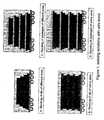
- FIG. 1illustrates a conventional approach to configuring die and packages with wire bond in both same size packages and different size packages.
- FIGS. 1A and 1Cillustrate different size die ( FIG. 1A ) and packages ( FIG. 1C ), where the stacking is on a stair case shape. In each package, connections must be made on the outside of the die edges, or otherwise made through the die substrates.
- FIGS. 1B and 1Dillustrate equal size die ( FIG. 1B ) and packages ( FIG. 1D ), where the stacking is on a rectangular configuration. Like the other package configurations illustrated in FIGS. 1A and 1C , in each package, connections must be made on the outside of the die edges, or otherwise made through the die substrates. In an assembly of the same size packages, a thick adhesive is used to clear the wire bond loop.
- a stacked chip packageis illustrated having solder balls in between same sized stacked layers of the package.
- wide variations in temperaturegreatly affect the ability to stack and connect the different layers.
- the connectionsare difficult to make from layer to layer, and are done upon processing and assembly of the package.
- Table 1compares and contrasts the features and benefits of three exemplary ways of stacking, i.e., solder ball stacking of equal sized packages, wire bond stacking of equal size packages, and wire bond stacking of different size packages.
- the configurationsare compared in terms of adhesive thickness, individual chip select, inventory management, package width, JEDEC ball out, and whether or not the die is exposed.
- a microelectronic circuit packagehaving a stacked array of a plurality of polymer tape elements.
- the polymer tape elementshave surface circuitization (e.g., leads, pads, and wiring) located on the surface. At least one of the polymer tape elements has a via or opening therein to pass wiring between elements within the periphery of the package.
- a microelectronic circuit packagehaving a stacked array of polymer tape elements.
- the polymer tape elementsare in stacked array one above another, where the polymer tape elements have surface circuitization. At least one of the polymer tape elements has a via therein.
- the package circuitizationincludes leads from a polymer tape element having the via therein to a next subjacent or superjacent polymer tape element.
- FIG. 1including FIGS. 1A, 1B , 1 C, and 1 D, denominated “Prior Art” illustrate exemplifications of multi-die and multi-package configurations including wiring interconnections.
- FIG. 2including FIGS. 2A and 2B , denominated “Prior Art” illustrate exemplifications of multi-die and multi-package configurations including wiring interconnections.
- FIG. 3illustrates one exemplification of our invention of a stacked array of polymer tape elements having the die in a face up configuration.
- FIG. 4illustrates one exemplification of our invention of a stacked array of polymer tape elements having the die in a face down configuration.
- FIG. 5illustrates another embodiment of the invention that maximizes electrical contacts in a chip package.
- microelectronic package configuration and the exemplary microelectronic packages described hereinprovide a multi-layer package that balances the competing demands of package size, adhesive thickness, chip access, inventory management, package width, JEDEC ball out, and die exposure. This is accomplished in a microelectronic circuit package having a stacked array of polymer tape elements.
- the polymer tape elementsare in stacked array one above another.
- the individual polymer tape elementshave surface circuitization.
- Intra-package connectivityis provided by routing some circuitization through an aperture, in the sense of a via or through hole, in at least one of the individual polymeric elements.
- the package circuitizationroutes circuitization from one polymeric tape element having a via therein to circuitization on another polymeric element, for example, to a next subjacent or superjacent polymeric tape element.
- the apertureas a window, exposes pads or other contacts of the packages below. This technique enables wire bonding in all packages from both edges of the die, while avoiding wire bonding outside the periphery of the package.
- the connectionscan be made through the apertures after assembly, allowing for variations in connections from one layer to another to provide further flexibility in design.
- the package described hereinis an assembly of TAB (Tape Automated Bonding) packages.
- a TAB tape known in the artcomprises an electrically insulating base film, such as polyimide, having a conductor pattern formed on the base film.
- One advantage of a TAB tapeis that it can provide an extremely fine conductor pattern.
- the circuitizationis fabricated by forming a conductive film, for example, copper foil and the like on polymer film and then etching the circuitization pattern in the film in the shape of a required pattern.
- a conductive filmfor example, copper foil and the like
- the conductor thin filmis supported on the polymeric base film of the TAB tape, and it therefore becomes possible to use a conductor which is much thinner than a conventional metal lead frame and to form a conductor pattern of high-density which cannot be formed by such a conventional metal lead frame.
- the base film of the TAB tapesupports the circuitization conductor pattern
- the polymeric base filmitself must have a low dielectric coefficient and low conductivity.
- this base filmmust be thermally rugged to withstand fabrication, since the TAB tape is hermetically sealed with resin after a semiconductor chip is mounted on thereon.
- a heat-resisting plastic filmsuch as polyimide film or the like is used as the base film.
- a conventional semiconductor device with a TAB tapeincludes the TAB tape and a semiconductor element or die.
- the TAB tapeis formed of an insulating organic polymer such as a polyimide film which has a frame-like shape.
- the polymeric filmis rectangular in shape, and has an uncircuitized rectangular area for attachment of the semiconductor device.
- a plurality of electrodesare arranged on the semiconductor device in a line along four sides thereof.
- the TAB elementcarries a plurality of signal lines and ground lines on the polymeric TAB element. These lines are formed, for instance, by depositing a thin metallic film such as a copper film on the polymeric element and wet-etching, dry etching, or ion beam etching the thin metallic film.
- the signal and ground linestypically extend inwardly from the film to electrically connect with the semiconductor electrodes.
- the signal and ground circuitizationextend outwardly beyond the TAB element.
- wire connectionscan be carried from one TAB element to another via apertures located on each tab.
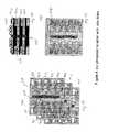
- FIGS. 3A, 3B , and 3 Cone embodiment of the invention is illustrated in an application where TABs are arrayed in a Ball Grid Array (“BGA”) in a “face up” configuration.
- BGABall Grid Array
- FIG. 3Aan exploded above view is shown of a package including a plurality of TAB 302 , 304 , 305 , elements, where the elements include apertures 306 - 334 substantially along the centerline 338 thereof.
- the aperturesare configured to carry wiring connected to electrical connections 340 , 342 , from semiconductor elements 344 , 346 mounted on a TAB element 304 to lower elements 302 , 305 or to a printed circuit board, card, or panel.
- FIG. 3Bshows a side view of an assembled package with tabs 302 , 304 , 305 , stacked. Wires 348 , 350 may extend from one TAB element to the next, or may skip from a top TAB element 304 directly to the other TAB elements, or to substrate 352 to connect to solder balls 354 .
- FIG. 3Ca top view of the package of FIG.
- the inventionprovides a means to freely connect from TAB to TAB and to the substrate of the package without the need for complicated interconnections among the TABs as in conventional methods and systems.
- wire connectionscan be carried from one TAB element to another via apertures located on each tab.
- FIGS. 4A, 4B , and 4 Cone embodiment of the invention is illustrated in an application where TABs are arrayed in a Ball Grid Array (“BGA”) in a “face down” configuration.
- BGABall Grid Array
- FIG. 4Aan exploded above view is shown of a package including a plurality of TAB 402 , 404 , 405 , elements, where the elements include apertures 406 - 434 substantially along the centerline 438 thereof.
- the aperturesare configured to carry wiring connected to electrical connections 440 , 442 , from semiconductor elements 444 , 446 mounted on a TAB element 404 to lower elements 402 , 405 or to a printed circuit board, card, or panel.
- FIG. 4Bshows a side view of an assembled package with tabs 402 , 404 , 405 , stacked. Wires 448 , 450 may extend from one TAB element to the next, or may skip from a top TAB element 404 directly to the other TAB elements, or to substrate 452 to connect to solder balls 454 .
- FIG. 4Ca view of the package from the bottom surface side 457 of FIG.
- the inventionprovides a means to freely connect from TAB to TAB and to the substrate of the package without the need for complicated interconnections among the TABs as in conventional methods and systems.
- the final packagecan be in face-up BGA type as illustrated in FIG. 3 , or in a face-down BGA as in FIG. 4 . Additionally, each package can be a JEDEC standard ball-out design.
- the aperturewas shown to be a single aperture normal to center pad axis of the die. However, this is only illustrative, and those skilled in the art will understand that there could be multiple apertures that could be arrayed at an arbitrary alignment. Openings could be slanted at any angle to accommodate different configurations. The exception may be openings that are parallel to the die center pad axis, which makes it difficult to perform wire bond processes.
- FIG. 5another embodiment of the invention is illustrated, where the contacts locate on the edges of the multiple layered dies are overlapped in a reverse fashion in comparison to the openings of the embodiments illustrated in FIGS. 3 and 4 and discussed above.
- FIG. 5 aa substrate 500 is illustrated in a trapezoidal shape, having rows of electrical contacts 502 , 504 .
- the configurationis adaptable to stacked substrates that may be either skewed or of various sizes to expose the electrical contacts for connection. Contacts can be set on two sides of a substrate, and modifying the shape of the substrates to maximize the edge length would increase the number of contacts on each utilized edge.
- FIGS. 5another embodiment of the invention is illustrated, where the contacts locate on the edges of the multiple layered dies are overlapped in a reverse fashion in comparison to the openings of the embodiments illustrated in FIGS. 3 and 4 and discussed above.
- FIG. 5 aa substrate 500 is illustrated in a trapezoidal shape, having rows of electrical contacts 502 , 504 .
- a chip package 505 of stacked substrates 500 , 506 , 508 , and 510is illustrated.
- the substratesare illustrated stacked in a skewed or otherwise offset manner in order to allow vertical access to the contact edges, such as 502 and 504 , so that processing is convenient.
- contact wires 512connect contacts from one substrate layer to the next, and ultimately to down to a base substrate 513 , through which solder balls 514 , 516 can be contacted.
- PWBprinted wiring board
- the solder ballsare placed into contact with outside devices.
- FIG. 5Ca top view of the package of 5 B is illustrated showing the access to the edge contacts 502 and 504 , as well as all other edges of the four substrates 500 , 506 , 508 and 510 .
- the base substrate 513is illustrated with edge contacts 518 , 520 that have a few wires 512 for illustration of contacting the edges of the several substrates and the base substrate.
Landscapes
- Engineering & Computer Science (AREA)
- Microelectronics & Electronic Packaging (AREA)
- Power Engineering (AREA)
- Physics & Mathematics (AREA)
- Condensed Matter Physics & Semiconductors (AREA)
- General Physics & Mathematics (AREA)
- Computer Hardware Design (AREA)
- Lead Frames For Integrated Circuits (AREA)
- Wire Bonding (AREA)
Abstract
Description
- This application claims priority from U.S. Provisional Patent Application No. 60/531,032 filed Dec. 19, 2003.
- In conventional stacked chip packaging systems and methods, a great deal of effort and cost is expended in connecting one layer to another and to an outside connection.
FIG. 1 illustrates a conventional approach to configuring die and packages with wire bond in both same size packages and different size packages.FIGS. 1A and 1C illustrate different size die (FIG. 1A ) and packages (FIG. 1C ), where the stacking is on a stair case shape. In each package, connections must be made on the outside of the die edges, or otherwise made through the die substrates.FIGS. 1B and 1D illustrate equal size die (FIG. 1B ) and packages (FIG. 1D ), where the stacking is on a rectangular configuration. Like the other package configurations illustrated inFIGS. 1A and 1C , in each package, connections must be made on the outside of the die edges, or otherwise made through the die substrates. In an assembly of the same size packages, a thick adhesive is used to clear the wire bond loop.- Referring to
FIG. 2 , a stacked chip package is illustrated having solder balls in between same sized stacked layers of the package. In processing such a package, wide variations in temperature greatly affect the ability to stack and connect the different layers. Also, the connections are difficult to make from layer to layer, and are done upon processing and assembly of the package. - Table 1 compares and contrasts the features and benefits of three exemplary ways of stacking, i.e., solder ball stacking of equal sized packages, wire bond stacking of equal size packages, and wire bond stacking of different size packages. The configurations are compared in terms of adhesive thickness, individual chip select, inventory management, package width, JEDEC ball out, and whether or not the die is exposed.
TABLE 1 Reported package stacking Solder ball stacking Wire bond stacking Package size Same Same Different Adhesive THIN THICK THIN (total package thickness) Chip select required YES NO NO in individual package Inventory issue YES NO YES Package width WIDE NARROW NARROW JEDEC ball out NO YES YES Exposed die YES NO NO
The comparison shows the need for a multi-level packaging strategy that optimizes the trade-off between package size, adhesive thickness, chip access, inventory management, package width, JEDEC ball out, and dies exposure. As will be seen, the invention optimizes these features in an elegant manner. - This balance of package size, adhesive thickness, chip access, inventory management, package width, JEDEC ball out, and die exposure is accomplished in a microelectronic circuit package having a stacked array of a plurality of polymer tape elements. The polymer tape elements have surface circuitization (e.g., leads, pads, and wiring) located on the surface. At least one of the polymer tape elements has a via or opening therein to pass wiring between elements within the periphery of the package.
- This balance of package size, adhesive thickness, chip access, inventory management, package width, JEDEC ball out, and die exposure is also accomplished in a microelectronic circuit package having a stacked array of polymer tape elements. The polymer tape elements are in stacked array one above another, where the polymer tape elements have surface circuitization. At least one of the polymer tape elements has a via therein. By this expedient the package circuitization includes leads from a polymer tape element having the via therein to a next subjacent or superjacent polymer tape element.
FIG. 1 includingFIGS. 1A, 1B ,1C, and1D, denominated “Prior Art” illustrate exemplifications of multi-die and multi-package configurations including wiring interconnections.FIG. 2 , includingFIGS. 2A and 2B , denominated “Prior Art” illustrate exemplifications of multi-die and multi-package configurations including wiring interconnections.FIG. 3 , includingFIGS. 3A, 3B , and3C, illustrates one exemplification of our invention of a stacked array of polymer tape elements having the die in a face up configuration.FIG. 4 , includingFIGS. 4A, 4B , and4C, illustrates one exemplification of our invention of a stacked array of polymer tape elements having the die in a face down configuration.FIG. 5 illustrates another embodiment of the invention that maximizes electrical contacts in a chip package.- The microelectronic package configuration and the exemplary microelectronic packages described herein provide a multi-layer package that balances the competing demands of package size, adhesive thickness, chip access, inventory management, package width, JEDEC ball out, and die exposure. This is accomplished in a microelectronic circuit package having a stacked array of polymer tape elements. The polymer tape elements are in stacked array one above another. The individual polymer tape elements have surface circuitization. Intra-package connectivity is provided by routing some circuitization through an aperture, in the sense of a via or through hole, in at least one of the individual polymeric elements. By this expedient the package circuitization routes circuitization from one polymeric tape element having a via therein to circuitization on another polymeric element, for example, to a next subjacent or superjacent polymeric tape element. The aperture, as a window, exposes pads or other contacts of the packages below. This technique enables wire bonding in all packages from both edges of the die, while avoiding wire bonding outside the periphery of the package. Furthermore, the connections can be made through the apertures after assembly, allowing for variations in connections from one layer to another to provide further flexibility in design.
- The package described herein is an assembly of TAB (Tape Automated Bonding) packages. A TAB tape known in the art comprises an electrically insulating base film, such as polyimide, having a conductor pattern formed on the base film. One advantage of a TAB tape is that it can provide an extremely fine conductor pattern.
- For producing a TAB tape, the circuitization is fabricated by forming a conductive film, for example, copper foil and the like on polymer film and then etching the circuitization pattern in the film in the shape of a required pattern. One advantage of TAB bonding is that the conductor thin film is supported on the polymeric base film of the TAB tape, and it therefore becomes possible to use a conductor which is much thinner than a conventional metal lead frame and to form a conductor pattern of high-density which cannot be formed by such a conventional metal lead frame.
- Because the base film of the TAB tape supports the circuitization conductor pattern, the polymeric base film itself must have a low dielectric coefficient and low conductivity. In addition, this base film must be thermally rugged to withstand fabrication, since the TAB tape is hermetically sealed with resin after a semiconductor chip is mounted on thereon. Thus, a heat-resisting plastic film such as polyimide film or the like is used as the base film.
- A conventional semiconductor device with a TAB tape includes the TAB tape and a semiconductor element or die. The TAB tape is formed of an insulating organic polymer such as a polyimide film which has a frame-like shape. Generally, the polymeric film is rectangular in shape, and has an uncircuitized rectangular area for attachment of the semiconductor device. A plurality of electrodes are arranged on the semiconductor device in a line along four sides thereof.
- The TAB element carries a plurality of signal lines and ground lines on the polymeric TAB element. These lines are formed, for instance, by depositing a thin metallic film such as a copper film on the polymeric element and wet-etching, dry etching, or ion beam etching the thin metallic film. The signal and ground lines typically extend inwardly from the film to electrically connect with the semiconductor electrodes. In addition, the signal and ground circuitization extend outwardly beyond the TAB element. When the semiconductor device is to be mounted on a circuit board or card, the signal and ground extending outwardly from the semiconductor device are electrically connected to electrodes formed on board, card, or panel.
- According to the invention, wire connections can be carried from one TAB element to another via apertures located on each tab. Referring to
FIGS. 3A, 3B , and3C, one embodiment of the invention is illustrated in an application where TABs are arrayed in a Ball Grid Array (“BGA”) in a “face up” configuration. Referring first toFIG. 3A , an exploded above view is shown of a package including a plurality ofTAB 302,304,305, elements, where the elements include apertures306-334 substantially along the centerline338 thereof. The apertures are configured to carry wiring connected to electrical connections340,342, from semiconductor elements344,346 mounted on aTAB element 304 to lower elements302,305 or to a printed circuit board, card, or panel.FIG. 3B shows a side view of an assembled package withtabs 302,304,305, stacked.Wires 348,350 may extend from one TAB element to the next, or may skip from atop TAB element 304 directly to the other TAB elements, or to substrate352 to connect to solder balls354. Referring toFIG. 3C , a top view of the package ofFIG. 3B is shown, illustrating thewire connections 356 emanating fromorifice 358 on the top of the package and connecting to semiconductor elements344,346. Thus, the invention provides a means to freely connect from TAB to TAB and to the substrate of the package without the need for complicated interconnections among the TABs as in conventional methods and systems. - According to the invention, wire connections can be carried from one TAB element to another via apertures located on each tab. Referring to
FIGS. 4A, 4B , and4C, one embodiment of the invention is illustrated in an application where TABs are arrayed in a Ball Grid Array (“BGA”) in a “face down” configuration. Referring first toFIG. 4A , an exploded above view is shown of a package including a plurality ofTAB centerline 438 thereof. The apertures are configured to carry wiring connected to electrical connections440,442, from semiconductor elements444,446 mounted on aTAB element 404 tolower elements 402,405 or to a printed circuit board, card, or panel.FIG. 4B shows a side view of an assembled package withtabs top TAB element 404 directly to the other TAB elements, or to substrate452 to connect to solder balls454. Referring toFIG. 4C , a view of the package from thebottom surface side 457 ofFIG. 4B is shown, illustrating thewire connections 456 emanating from orifice458 on the top of the package and connecting to semiconductor elements444,446. Thus, the invention provides a means to freely connect from TAB to TAB and to the substrate of the package without the need for complicated interconnections among the TABs as in conventional methods and systems. - The final package can be in face-up BGA type as illustrated in
FIG. 3 , or in a face-down BGA as inFIG. 4 . Additionally, each package can be a JEDEC standard ball-out design. InFIGS. 3 and 4 the aperture was shown to be a single aperture normal to center pad axis of the die. However, this is only illustrative, and those skilled in the art will understand that there could be multiple apertures that could be arrayed at an arbitrary alignment. Openings could be slanted at any angle to accommodate different configurations. The exception may be openings that are parallel to the die center pad axis, which makes it difficult to perform wire bond processes. - Referring to
FIG. 5 , another embodiment of the invention is illustrated, where the contacts locate on the edges of the multiple layered dies are overlapped in a reverse fashion in comparison to the openings of the embodiments illustrated inFIGS. 3 and 4 and discussed above.FIG. 5 a,asubstrate 500 is illustrated in a trapezoidal shape, having rows ofelectrical contacts 502,504. The configuration is adaptable to stacked substrates that may be either skewed or of various sizes to expose the electrical contacts for connection. Contacts can be set on two sides of a substrate, and modifying the shape of the substrates to maximize the edge length would increase the number of contacts on each utilized edge. Similarly, and referring back to the configurations illustrated inFIGS. 3 and 4 , if the openings were configured as trapezoids or other shape that optimizes the edges on which the contacts are located, then the number of contacts can be maximized. Referring toFIG. 5B , a chip package505 of stackedsubstrates - In fabrication, it is important to allow contact with the electrical contacts located on the edges of the substrate, so that conventional processing equipment can make connections with contacts with wires or other electrical contact means. According to the invention, whether the contacts occur on the inside edge of an orifice or on a maximized contact edge, increased contact edges are achieved, and thus more contacts.
- Still referring to
FIG. 5B , contact wires512 connect contacts from one substrate layer to the next, and ultimately to down to a base substrate513, through whichsolder balls FIG. 5C , a top view of the package of5B is illustrated showing the access to theedge contacts 502 and504, as well as all other edges of the foursubstrates edge contacts - While the foregoing description has been with reference to particular embodiments of the invention, it will be appreciated that these are only illustrative of the invention and the changes may be made to those embodiments without departing from the principles of invention, the scope of which is defined by the appended claims.
Claims (9)
Priority Applications (1)
| Application Number | Priority Date | Filing Date | Title |
|---|---|---|---|
| US11/014,506US7989940B2 (en) | 2003-12-19 | 2004-12-15 | System and method for increasing the number of IO-s on a ball grid package by wire bond stacking of same size packages through apertures |
Applications Claiming Priority (2)
| Application Number | Priority Date | Filing Date | Title |
|---|---|---|---|
| US53103203P | 2003-12-19 | 2003-12-19 | |
| US11/014,506US7989940B2 (en) | 2003-12-19 | 2004-12-15 | System and method for increasing the number of IO-s on a ball grid package by wire bond stacking of same size packages through apertures |
Publications (2)
| Publication Number | Publication Date |
|---|---|
| US20050133899A1true US20050133899A1 (en) | 2005-06-23 |
| US7989940B2 US7989940B2 (en) | 2011-08-02 |
Family
ID=34680925
Family Applications (1)
| Application Number | Title | Priority Date | Filing Date |
|---|---|---|---|
| US11/014,506Expired - Fee RelatedUS7989940B2 (en) | 2003-12-19 | 2004-12-15 | System and method for increasing the number of IO-s on a ball grid package by wire bond stacking of same size packages through apertures |
Country Status (1)
| Country | Link |
|---|---|
| US (1) | US7989940B2 (en) |
Cited By (1)
| Publication number | Priority date | Publication date | Assignee | Title |
|---|---|---|---|---|
| US11270963B2 (en) | 2020-01-14 | 2022-03-08 | Sandisk Technologies Llc | Bonding pads including interfacial electromigration barrier layers and methods of making the same |
Families Citing this family (27)
| Publication number | Priority date | Publication date | Assignee | Title |
|---|---|---|---|---|
| KR20110050964A (en)* | 2009-11-09 | 2011-05-17 | 주식회사 하이닉스반도체 | Semiconductor package and manufacturing method thereof |
| US8823165B2 (en) | 2011-07-12 | 2014-09-02 | Invensas Corporation | Memory module in a package |
| US8513817B2 (en) | 2011-07-12 | 2013-08-20 | Invensas Corporation | Memory module in a package |
| US8502390B2 (en) | 2011-07-12 | 2013-08-06 | Tessera, Inc. | De-skewed multi-die packages |
| US8405207B1 (en) | 2011-10-03 | 2013-03-26 | Invensas Corporation | Stub minimization for wirebond assemblies without windows |
| US8345441B1 (en) | 2011-10-03 | 2013-01-01 | Invensas Corporation | Stub minimization for multi-die wirebond assemblies with parallel windows |
| US8525327B2 (en) | 2011-10-03 | 2013-09-03 | Invensas Corporation | Stub minimization for assemblies without wirebonds to package substrate |
| US8441111B2 (en) | 2011-10-03 | 2013-05-14 | Invensas Corporation | Stub minimization for multi-die wirebond assemblies with parallel windows |
| JP5947904B2 (en) | 2011-10-03 | 2016-07-06 | インヴェンサス・コーポレイション | Stub minimization for multi-die wirebond assemblies with orthogonal windows |
| US8436457B2 (en) | 2011-10-03 | 2013-05-07 | Invensas Corporation | Stub minimization for multi-die wirebond assemblies with parallel windows |
| TWI515864B (en) | 2011-10-03 | 2016-01-01 | 英帆薩斯公司 | Stub minimization with terminal grids offset from center of package |
| US8436477B2 (en) | 2011-10-03 | 2013-05-07 | Invensas Corporation | Stub minimization using duplicate sets of signal terminals in assemblies without wirebonds to package substrate |
| US8653646B2 (en) | 2011-10-03 | 2014-02-18 | Invensas Corporation | Stub minimization using duplicate sets of terminals for wirebond assemblies without windows |
| KR101894823B1 (en) | 2011-10-03 | 2018-09-04 | 인벤사스 코포레이션 | Stub minimization for multi-die wirebond assemblies with parallel windows |
| US8787034B2 (en) | 2012-08-27 | 2014-07-22 | Invensas Corporation | Co-support system and microelectronic assembly |
| US8848392B2 (en) | 2012-08-27 | 2014-09-30 | Invensas Corporation | Co-support module and microelectronic assembly |
| US9368477B2 (en) | 2012-08-27 | 2016-06-14 | Invensas Corporation | Co-support circuit panel and microelectronic packages |
| US8848391B2 (en) | 2012-08-27 | 2014-09-30 | Invensas Corporation | Co-support component and microelectronic assembly |
| US9853053B2 (en) | 2012-09-10 | 2017-12-26 | 3B Technologies, Inc. | Three dimension integrated circuits employing thin film transistors |
| US9070423B2 (en) | 2013-06-11 | 2015-06-30 | Invensas Corporation | Single package dual channel memory with co-support |
| US9123555B2 (en) | 2013-10-25 | 2015-09-01 | Invensas Corporation | Co-support for XFD packaging |
| US9281296B2 (en) | 2014-07-31 | 2016-03-08 | Invensas Corporation | Die stacking techniques in BGA memory package for small footprint CPU and memory motherboard design |
| US9691437B2 (en) | 2014-09-25 | 2017-06-27 | Invensas Corporation | Compact microelectronic assembly having reduced spacing between controller and memory packages |
| WO2016099580A2 (en) | 2014-12-23 | 2016-06-23 | Lupino James John | Three dimensional integrated circuits employing thin film transistors |
| US9484080B1 (en) | 2015-11-09 | 2016-11-01 | Invensas Corporation | High-bandwidth memory application with controlled impedance loading |
| KR102413441B1 (en) | 2015-11-12 | 2022-06-28 | 삼성전자주식회사 | Semiconductor package |
| US9679613B1 (en) | 2016-05-06 | 2017-06-13 | Invensas Corporation | TFD I/O partition for high-speed, high-density applications |
Citations (9)
| Publication number | Priority date | Publication date | Assignee | Title |
|---|---|---|---|---|
| US4996587A (en)* | 1989-04-10 | 1991-02-26 | International Business Machines Corporation | Integrated semiconductor chip package |
| US5373189A (en)* | 1992-08-13 | 1994-12-13 | Commissariate A L'energie Atomique | Three-dimensional multichip module |
| US5422435A (en)* | 1992-05-22 | 1995-06-06 | National Semiconductor Corporation | Stacked multi-chip modules and method of manufacturing |
| US5679977A (en)* | 1990-09-24 | 1997-10-21 | Tessera, Inc. | Semiconductor chip assemblies, methods of making same and components for same |
| US5870289A (en)* | 1994-12-15 | 1999-02-09 | Hitachi, Ltd. | Chip connection structure having diret through-hole connections through adhesive film and wiring substrate |
| US5903049A (en)* | 1997-10-29 | 1999-05-11 | Mitsubishi Denki Kabushiki Kaisha | Semiconductor module comprising semiconductor packages |
| US6180881B1 (en)* | 1998-05-05 | 2001-01-30 | Harlan Ruben Isaak | Chip stack and method of making same |
| US20030162326A1 (en)* | 1996-11-21 | 2003-08-28 | Kunihiro Tsubosaki | Semiconductor device and manufactuiring method thereof |
| US7180312B2 (en)* | 2002-03-28 | 2007-02-20 | Fujitsu Limited | Probe card and method for manufacturing probe card |
- 2004
- 2004-12-15USUS11/014,506patent/US7989940B2/ennot_activeExpired - Fee Related
Patent Citations (9)
| Publication number | Priority date | Publication date | Assignee | Title |
|---|---|---|---|---|
| US4996587A (en)* | 1989-04-10 | 1991-02-26 | International Business Machines Corporation | Integrated semiconductor chip package |
| US5679977A (en)* | 1990-09-24 | 1997-10-21 | Tessera, Inc. | Semiconductor chip assemblies, methods of making same and components for same |
| US5422435A (en)* | 1992-05-22 | 1995-06-06 | National Semiconductor Corporation | Stacked multi-chip modules and method of manufacturing |
| US5373189A (en)* | 1992-08-13 | 1994-12-13 | Commissariate A L'energie Atomique | Three-dimensional multichip module |
| US5870289A (en)* | 1994-12-15 | 1999-02-09 | Hitachi, Ltd. | Chip connection structure having diret through-hole connections through adhesive film and wiring substrate |
| US20030162326A1 (en)* | 1996-11-21 | 2003-08-28 | Kunihiro Tsubosaki | Semiconductor device and manufactuiring method thereof |
| US5903049A (en)* | 1997-10-29 | 1999-05-11 | Mitsubishi Denki Kabushiki Kaisha | Semiconductor module comprising semiconductor packages |
| US6180881B1 (en)* | 1998-05-05 | 2001-01-30 | Harlan Ruben Isaak | Chip stack and method of making same |
| US7180312B2 (en)* | 2002-03-28 | 2007-02-20 | Fujitsu Limited | Probe card and method for manufacturing probe card |
Cited By (1)
| Publication number | Priority date | Publication date | Assignee | Title |
|---|---|---|---|---|
| US11270963B2 (en) | 2020-01-14 | 2022-03-08 | Sandisk Technologies Llc | Bonding pads including interfacial electromigration barrier layers and methods of making the same |
Also Published As
| Publication number | Publication date |
|---|---|
| US7989940B2 (en) | 2011-08-02 |
Similar Documents
| Publication | Publication Date | Title |
|---|---|---|
| US7989940B2 (en) | System and method for increasing the number of IO-s on a ball grid package by wire bond stacking of same size packages through apertures | |
| US10804139B2 (en) | Semiconductor system | |
| US7843053B2 (en) | Stack package made of chip scale packages | |
| US5744862A (en) | Reduced thickness semiconductor device with IC packages mounted in openings on substrate | |
| US7129420B2 (en) | Semiconductor device and method for manufacture thereof, circuit board, and electronic instrument | |
| US6552423B2 (en) | Higher-density memory card | |
| US6441476B1 (en) | Flexible tape carrier with external terminals formed on interposers | |
| KR101521254B1 (en) | Double-molded multi-chip package system | |
| US8039365B2 (en) | Integrated circuit package system including wafer level spacer | |
| US11031371B2 (en) | Semiconductor package and method of fabricating semiconductor package | |
| US8294251B2 (en) | Stacked semiconductor package with localized cavities for wire bonding | |
| US7078792B2 (en) | Universal interconnect die | |
| US8470640B2 (en) | Method of fabricating stacked semiconductor package with localized cavities for wire bonding | |
| US6770980B2 (en) | Semiconductor device having semiconductor element packaged on interposer | |
| US7042104B2 (en) | Semiconductor package using flexible film and method of manufacturing the same | |
| KR100866137B1 (en) | Stack package | |
| US7884465B2 (en) | Semiconductor package with passive elements embedded within a semiconductor chip | |
| US12051680B2 (en) | Semiconductor package aligning interposer and substrate | |
| KR100256306B1 (en) | Stacked Multi-Chip Modules | |
| JPH09321218A (en) | Semiconductor device and manufacturing method thereof | |
| KR20080090012A (en) | Chip having dimple, manufacturing method thereof and package using the chip | |
| KR20070052911A (en) | Stacked Package |
Legal Events
| Date | Code | Title | Description |
|---|---|---|---|
| AS | Assignment | Owner name:TESSERA, INC., CALIFORNIA Free format text:ASSIGNMENT OF ASSIGNORS INTEREST;ASSIGNORS:HABA, BELGACEM;BEROZ, MASUD;REEL/FRAME:015694/0011 Effective date:20041215 | |
| STCF | Information on status: patent grant | Free format text:PATENTED CASE | |
| FPAY | Fee payment | Year of fee payment:4 | |
| AS | Assignment | Owner name:ROYAL BANK OF CANADA, AS COLLATERAL AGENT, CANADA Free format text:SECURITY INTEREST;ASSIGNORS:INVENSAS CORPORATION;TESSERA, INC.;TESSERA ADVANCED TECHNOLOGIES, INC.;AND OTHERS;REEL/FRAME:040797/0001 Effective date:20161201 | |
| FEPP | Fee payment procedure | Free format text:MAINTENANCE FEE REMINDER MAILED (ORIGINAL EVENT CODE: REM.); ENTITY STATUS OF PATENT OWNER: LARGE ENTITY | |
| LAPS | Lapse for failure to pay maintenance fees | Free format text:PATENT EXPIRED FOR FAILURE TO PAY MAINTENANCE FEES (ORIGINAL EVENT CODE: EXP.); ENTITY STATUS OF PATENT OWNER: LARGE ENTITY | |
| STCH | Information on status: patent discontinuation | Free format text:PATENT EXPIRED DUE TO NONPAYMENT OF MAINTENANCE FEES UNDER 37 CFR 1.362 | |
| FP | Lapsed due to failure to pay maintenance fee | Effective date:20190802 | |
| AS | Assignment | Owner name:INVENSAS CORPORATION, CALIFORNIA Free format text:RELEASE BY SECURED PARTY;ASSIGNOR:ROYAL BANK OF CANADA;REEL/FRAME:052920/0001 Effective date:20200601 Owner name:DTS LLC, CALIFORNIA Free format text:RELEASE BY SECURED PARTY;ASSIGNOR:ROYAL BANK OF CANADA;REEL/FRAME:052920/0001 Effective date:20200601 Owner name:IBIQUITY DIGITAL CORPORATION, MARYLAND Free format text:RELEASE BY SECURED PARTY;ASSIGNOR:ROYAL BANK OF CANADA;REEL/FRAME:052920/0001 Effective date:20200601 Owner name:INVENSAS BONDING TECHNOLOGIES, INC. (F/K/A ZIPTRONIX, INC.), CALIFORNIA Free format text:RELEASE BY SECURED PARTY;ASSIGNOR:ROYAL BANK OF CANADA;REEL/FRAME:052920/0001 Effective date:20200601 Owner name:FOTONATION CORPORATION (F/K/A DIGITALOPTICS CORPORATION AND F/K/A DIGITALOPTICS CORPORATION MEMS), CALIFORNIA Free format text:RELEASE BY SECURED PARTY;ASSIGNOR:ROYAL BANK OF CANADA;REEL/FRAME:052920/0001 Effective date:20200601 Owner name:DTS, INC., CALIFORNIA Free format text:RELEASE BY SECURED PARTY;ASSIGNOR:ROYAL BANK OF CANADA;REEL/FRAME:052920/0001 Effective date:20200601 Owner name:PHORUS, INC., CALIFORNIA Free format text:RELEASE BY SECURED PARTY;ASSIGNOR:ROYAL BANK OF CANADA;REEL/FRAME:052920/0001 Effective date:20200601 Owner name:TESSERA ADVANCED TECHNOLOGIES, INC, CALIFORNIA Free format text:RELEASE BY SECURED PARTY;ASSIGNOR:ROYAL BANK OF CANADA;REEL/FRAME:052920/0001 Effective date:20200601 Owner name:TESSERA, INC., CALIFORNIA Free format text:RELEASE BY SECURED PARTY;ASSIGNOR:ROYAL BANK OF CANADA;REEL/FRAME:052920/0001 Effective date:20200601 |