US20050133851A1 - Vertical NAND flash memory array - Google Patents
Vertical NAND flash memory arrayDownload PDFInfo
- Publication number
- US20050133851A1 US20050133851A1US10/738,556US73855603AUS2005133851A1US 20050133851 A1US20050133851 A1US 20050133851A1US 73855603 AUS73855603 AUS 73855603AUS 2005133851 A1US2005133851 A1US 2005133851A1
- Authority
- US
- United States
- Prior art keywords
- floating gate
- nand architecture
- forming
- memory
- memory cells
- Prior art date
- Legal status (The legal status is an assumption and is not a legal conclusion. Google has not performed a legal analysis and makes no representation as to the accuracy of the status listed.)
- Granted
Links
- 230000015654memoryEffects0.000titleclaimsabstractdescription306
- 238000007667floatingMethods0.000claimsabstractdescription159
- 238000000034methodMethods0.000claimsabstractdescription36
- 239000012212insulatorSubstances0.000claimsdescription69
- 239000000758substrateSubstances0.000claimsdescription52
- 238000002955isolationMethods0.000claimsdescription14
- 229910021420polycrystalline siliconInorganic materials0.000claimsdescription12
- 229920005591polysiliconPolymers0.000claimsdescription12
- 230000000873masking effectEffects0.000claimsdescription9
- 238000002347injectionMethods0.000claimsdescription8
- 239000007924injectionSubstances0.000claimsdescription8
- 238000005530etchingMethods0.000claimsdescription7
- 230000015572biosynthetic processEffects0.000claimsdescription6
- 238000000151depositionMethods0.000claimsdescription5
- 239000002784hot electronSubstances0.000claimsdescription4
- 230000005641tunnelingEffects0.000claimsdescription4
- 238000003491arrayMethods0.000abstractdescription24
- 239000004065semiconductorSubstances0.000abstractdescription11
- 230000008901benefitEffects0.000abstractdescription8
- 238000004519manufacturing processMethods0.000abstractdescription6
- 238000004513sizingMethods0.000abstractdescription4
- 238000005516engineering processMethods0.000description7
- 239000000463materialSubstances0.000description5
- 230000003213activating effectEffects0.000description3
- 239000011159matrix materialSubstances0.000description3
- XUIMIQQOPSSXEZ-UHFFFAOYSA-NSiliconChemical compound[Si]XUIMIQQOPSSXEZ-UHFFFAOYSA-N0.000description2
- 238000010586diagramMethods0.000description2
- 229910052594sapphireInorganic materials0.000description2
- 239000010980sapphireSubstances0.000description2
- 229910052710siliconInorganic materials0.000description2
- 239000010703siliconSubstances0.000description2
- 238000003860storageMethods0.000description2
- 239000010409thin filmSubstances0.000description2
- 230000006978adaptationEffects0.000description1
- 238000004891communicationMethods0.000description1
- 238000013500data storageMethods0.000description1
- 230000009977dual effectEffects0.000description1
- 230000000694effectsEffects0.000description1
- 230000005611electricityEffects0.000description1
- 230000005669field effectEffects0.000description1
- 230000006870functionEffects0.000description1
- 238000000059patterningMethods0.000description1
Images


Classifications
- H—ELECTRICITY
- H10—SEMICONDUCTOR DEVICES; ELECTRIC SOLID-STATE DEVICES NOT OTHERWISE PROVIDED FOR
- H10B—ELECTRONIC MEMORY DEVICES
- H10B41/00—Electrically erasable-and-programmable ROM [EEPROM] devices comprising floating gates
- H10B41/20—Electrically erasable-and-programmable ROM [EEPROM] devices comprising floating gates characterised by three-dimensional arrangements, e.g. with cells on different height levels
- H10B41/23—Electrically erasable-and-programmable ROM [EEPROM] devices comprising floating gates characterised by three-dimensional arrangements, e.g. with cells on different height levels with source and drain on different levels, e.g. with sloping channels
- H10B41/27—Electrically erasable-and-programmable ROM [EEPROM] devices comprising floating gates characterised by three-dimensional arrangements, e.g. with cells on different height levels with source and drain on different levels, e.g. with sloping channels the channels comprising vertical portions, e.g. U-shaped channels
- H—ELECTRICITY
- H10—SEMICONDUCTOR DEVICES; ELECTRIC SOLID-STATE DEVICES NOT OTHERWISE PROVIDED FOR
- H10B—ELECTRONIC MEMORY DEVICES
- H10B69/00—Erasable-and-programmable ROM [EPROM] devices not provided for in groups H10B41/00 - H10B63/00, e.g. ultraviolet erasable-and-programmable ROM [UVEPROM] devices
- H—ELECTRICITY
- H10—SEMICONDUCTOR DEVICES; ELECTRIC SOLID-STATE DEVICES NOT OTHERWISE PROVIDED FOR
- H10D—INORGANIC ELECTRIC SEMICONDUCTOR DEVICES
- H10D30/00—Field-effect transistors [FET]
- H10D30/60—Insulated-gate field-effect transistors [IGFET]
- H10D30/68—Floating-gate IGFETs
- H10D30/681—Floating-gate IGFETs having only two programming levels
- H10D30/683—Floating-gate IGFETs having only two programming levels programmed by tunnelling of carriers, e.g. Fowler-Nordheim tunnelling
- H—ELECTRICITY
- H10—SEMICONDUCTOR DEVICES; ELECTRIC SOLID-STATE DEVICES NOT OTHERWISE PROVIDED FOR
- H10D—INORGANIC ELECTRIC SEMICONDUCTOR DEVICES
- H10D30/00—Field-effect transistors [FET]
- H10D30/60—Insulated-gate field-effect transistors [IGFET]
- H10D30/68—Floating-gate IGFETs
- H10D30/681—Floating-gate IGFETs having only two programming levels
- H10D30/684—Floating-gate IGFETs having only two programming levels programmed by hot carrier injection
- H10D30/685—Floating-gate IGFETs having only two programming levels programmed by hot carrier injection from the channel
- G—PHYSICS
- G11—INFORMATION STORAGE
- G11C—STATIC STORES
- G11C16/00—Erasable programmable read-only memories
- G11C16/02—Erasable programmable read-only memories electrically programmable
- G11C16/04—Erasable programmable read-only memories electrically programmable using variable threshold transistors, e.g. FAMOS
- G11C16/0483—Erasable programmable read-only memories electrically programmable using variable threshold transistors, e.g. FAMOS comprising cells having several storage transistors connected in series
Definitions
- the present inventionrelates generally to integrated circuits and in particular the present invention relates to NAND architecture Flash memory devices.
- RAMrandom-access memory
- RAMrandom-access memory
- ROMread-only memory
- Most RAMis volatile, which means that it requires a steady flow of electricity to maintain its contents. As soon as the power is turned off, whatever data was in RAM is lost.
- EEPROMelectrically erasable programmable read-only memory
- EEPROMelectrically erasable programmable read-only memory
- EEPROMcomprise a large number of memory cells having electrically isolated gates (floating gates). Data is stored in the memory cells in the form of charge on the floating gates. Charge is transported to or removed from the floating gates by specialized programming and erase operations, respectively.
- Flash memoryis a type of EEPROM that is typically erased and reprogrammed in blocks instead of one byte at a time.
- a typical Flash memorycomprises a memory array, which includes a large number of memory cells. Each of the memory cells includes a floating gate field-effect transistor capable of holding a charge. The data in a cell is determined by the presence or absence of the charge in the floating gate.
- the cellsare usually grouped into sections called “erase blocks.”
- the memory cells of a Flash memory arrayare typically arranged into a “NOR” architecture (each cell directly coupled to a bit line) or a “NAND” architecture (cells coupled into “strings” of cells, such that each cell is coupled indirectly to a bit line and requires activating the other cells of the string for access).
- Each of the cells within an erase blockcan be electrically programmed in a random basis by charging the floating gate. The charge can be removed from the floating gate by a block erase operation, wherein all floating gate memory cells in the erase block are erased in a single operation.
- the feature sizes of the devicesare limited by the device characteristics before the minimum feature size that the process is capable of is reached.
- NAND Flash memory arraysin particular, as the channel length is reduced and the spacing between memory cells in the strings are reduced, a minimum size is reached that is primarily dictated by the operational characteristics of the floating gate memory cell devices that make up the memory strings.
- NAND architecture Flash memory devices and arraysin accordance with embodiments of the present invention, facilitate the utilization of NAND architecture floating gate memory cells in high density memory arrays or NAND strings.
- Memory embodiments of the present inventionutilize vertical Flash memory cells to form NAND architecture memory cell strings and memory arrays. These vertical memory cell NAND architecture strings allow for improved high density memory devices or arrays that can take advantage of the feature sizes semiconductor fabrication processes are generally capable of and still allow for appropriate device sizing for operational considerations.
- the inventionprovides a vertical floating gate memory cell string comprising a substrate, comprising one or more raised areas, defining trenches therebetween, a plurality of floating gate memory cells, wherein the floating gate memory cells are formed vertically on the sidewalls of one or more raised areas and/or trenches, and wherein the plurality of floating gate memory cells are coupled in a serial string by source/drain regions formed at the top of the one or more raised areas and at the bottom of the one or more trenches.
- the inventionprovides a vertical floating gate NAND architecture memory array comprising a substrate, comprising a plurality of pillars and associated intervening trenches, a plurality of floating gate memory cells, wherein the floating gate memory cells are formed vertically on the sidewalls of the plurality of pillars and trenches, and wherein the plurality of floating gate memory cells are coupled into a plurality of NAND architecture memory strings by source/drain regions formed at the top of the plurality of pillars and at the bottom of the associated trenches.
- the inventionprovides a system comprising a processor coupled to at least one memory device.
- the at least one memory devicecomprising a NAND architecture memory array formed on a substrate having a plurality of pillars and associated intervening trenches, a plurality of floating gate memory cells, wherein the floating gate memory cells are formed vertically on the sidewalls of the plurality of pillars and trenches, and wherein the plurality of floating gate cells are coupled into a plurality of NAND architecture memory strings by source/drain regions formed at the top of the plurality of pillars and at the bottom of the associated trenches.
- the inventionprovides a method of forming a vertical floating gate NAND architecture memory cell string comprising forming one or more raised areas on a substrate, the raised areas defining associated intervening trenches, forming a plurality of floating gate memory cells on the sidewalls of the one or more raised areas, and forming one or more source/drain regions on the top of the one or more raised areas and at the bottom of the one or more associated intervening trenches.
- the inventionprovides a method of forming a vertical floating gate NAND architecture memory array comprising forming a plurality of pillars and associated intervening trenches on a substrate, forming a plurality of vertical floating gate memory cells on the sidewalls of the plurality of pillars, and forming one or more source/drain regions on the top of the plurality of pillars and at the bottom of the associated intervening trenches to form a plurality of NAND architecture memory strings.
- FIGS. 1A and 1Bdetail a planar NAND Flash memory array of the prior art.
- FIGS. 2A-2Ddetail vertical NAND Flash memory array strings in accordance with embodiments of the present invention.
- FIGS. 3A and 3Bdetail vertical floating gate memory cells in accordance with embodiments of the present invention.
- FIGS. 4A and 4Bdetail a vertical NAND string and corresponding circuit in accordance with embodiments of the present invention.
- FIG. 5details a block diagram of an electronic system in accordance with embodiments of the present invention.
- Memory strings, arrays, and devices in accordance with embodiments of the present inventionfacilitate the use of floating gate memory cells in high density vertical NAND architecture memory strings, arrays, and devices.
- Memory embodiments of the present inventioninclude vertical Flash memory cells to form NAND architecture memory cell strings and memory arrays. These vertical memory cell NAND architecture strings allow for an improved high density memory devices or arrays that can take advantage of the feature sizes semiconductor fabrication processes are generally capable of and still allow for appropriate device sizing for operational considerations.
- Flash memory array architecturesare the “NAND” and “NOR” architectures, so called for the similarity each basic memory cell configuration has to the corresponding logic gate design.
- the floating gate memory cells of the memory arrayare arranged in a matrix similar to RAM or ROM.
- the gates of each floating gate memory cell of the array matrixare coupled by rows to word select lines (word lines) and their drains are coupled to column bit lines.
- the source of each floating gate memory cellis typically coupled to a common source line.
- the NOR architecture floating gate memory arrayis accessed by a row decoder activating a row of floating gate memory cells by selecting the word line coupled to their gates.
- the row of selected memory cellsthen place their stored data values on the column bit lines by flowing a differing current from the coupled source line to the coupled column bit lines depending on their programmed states.
- a column page of bit linesis selected and sensed, and individual data words are selected from the sensed data words from the column page and communicated from the Flash memory.
- a NAND array architecturealso arranges its array of floating gate memory cells in a matrix such that the gates of each floating gate memory cell of the array are coupled by rows to word lines. However each memory cell is not directly coupled to a source line and a column bit line. Instead, the memory cells of the array are arranged together in strings, typically of 8, 16, 32, or more each, where the memory cells in the string are coupled together in series, source to drain, between a common source line and a column bit line. This allows a NAND Flash array architecture to have a higher memory cell density than a comparable NOR Flash array, but with the cost of a generally slower access rate and programming complexity.
- a NAND architecture floating gate memory arrayis accessed by a row decoder activating a row of floating gate memory cells by selecting the word select line coupled to their gates.
- the word lines coupled to the gates of the unselected memory cells of each stringare also driven.
- the unselected memory cells of each stringare typically driven by a higher gate voltage so as to operate them as pass transistors and allowing them to pass current in a manner that is unrestricted by their stored data values.
- Currentthen flows from the source line to the column bit line through each floating gate memory cell of the series coupled string, restricted only by the memory cells of each string that are selected to be read. This places the current encoded stored data values of the row of selected memory cells on the column bit lines.
- a column page of bit linesis selected and sensed, and then individual data words are selected from the sensed data words from the column page and communicated from the Flash memory.
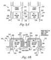
- FIGS. 1A and 1Bshow a simplified planar NAND Flash memory array of the prior art.
- FIG. 1Adetails a top view of a planar NAND Flash memory string 104 of a NAND Flash memory array 100
- a side view of the planar NAND Flash memory string 104is detailed in FIG. 1B .
- a series of floating gate memory cells 102are coupled together in a series NAND string 104 (typically of 8, 16, 32, or more cells).
- Each floating gate memory cell 102has a gate-insulator stack that is made of a tunnel insulator on top of a substrate 108 , a floating gate formed on the tunnel insulator, an intergate/interpoly insulator formed over the floating gate, and a control gate 106 (typically formed in a control gate line, also known as a word line) formed over the intergate/interpoly insulator.
- N+ doped regionsare formed between each gate insulator stack to form the source and drain regions of the adjacent floating gate memory cells, which additionally operate as connectors to couple the cells of the NAND string 104 together.
- Select gates 110that are coupled to gate select lines, are formed at either end of the NAND floating gate string 104 and selectively couple opposite ends of the NAND floating gate string 104 to a bit line contact 112 and a source line contact 114 .
- FIGS. 2A-2Ddetail vertical Flash cells and NAND architecture Flash memory strings in accordance with embodiments of the present invention.
- FIG. 2Adetails a side view of a simplified vertical NAND architecture Flash memory array string 204 of a NAND architecture Flash memory array 200
- a top view of the vertical NAND Flash memory array 200is detailed in FIG. 2C showing sections of two vertical NAND Flash memory array strings 204 .
- a three dimensional view of the vertical NAND Flash memory array 200is detailed in FIG. 2D .
- Methods of forming vertical memory cellsare detailed in U.S. Pat. No. 5,936,274, titled “High density flash memory”, issued Aug. 10, 1999, which is commonly assigned. Methods of forming vertical split control gates are detailed U.S. Pat. No.
- a series of vertically formed floating gate memory cells 202are coupled together in a series NAND string 204 (typically of 8, 16, 32, or more cells).
- a series NAND string 204typically of 8, 16, 32, or more cells.
- a series of substrate pillars 228are formed in a substrate 208 with trenches 230 located between them.
- the vertical floating gate memory cells 202are then formed on the sidewalls of the pillars 228 within the trenches 230 .
- Each vertical floating gate memory cell 202is formed on the sidewalls of the substrate pillars 228 (for two floating gate memory cells 202 per trench 230 ) and has a gate-insulator stack made of a tunnel insulator 220 formed on the surface of the sidewall, a floating gate 222 (typically of polysilicon) formed on the tunnel insulator 220 , an intergate/interpoly insulator 224 formed over the floating gate 222 , and a control gate 206 (typically formed in a control gate line, also known as a word line) formed over the intergate/interpoly insulator 224 .
- a gate-insulator stackmade of a tunnel insulator 220 formed on the surface of the sidewall, a floating gate 222 (typically of polysilicon) formed on the tunnel insulator 220 , an intergate/interpoly insulator 224 formed over the floating gate 222 , and a control gate 206 (typically formed in a control gate line, also known as a word line)
- the substrate pillars 228 and trenches 230are formed by patterning a masking material that is layered over the substrate 208 and anisotropically etching the trenches 230 .
- the gate-insulator stack of each floating gate memory cell 202are formed in one embodiment by successive layering of each of the materials of the gate insulator stack over the pillars 228 and trenches 230 , followed by a mask and directional etch of the deposit of each layer to leave only the material deposited on the sidewall of the pillars 228 .
- differing layers of the gate-insulator stackare formed and then masked and directionally etched in a single step.
- N+ doped regions 226are formed at the top of the substrate pillars 228 and at the bottom of the trenches 230 between each vertical floating gate memory cell/gate-insulator stack 202 to form the source and drain regions of the adjacent floating gate memory cells 202 and couple the memory cells 202 together to form the vertical NAND architecture memory string 204 . It is noted that the N+ source/drain regions 226 may be formed before or after the formation of the floating gate memory cells/gate-insulator stack 202 .
- Select gates 210that are coupled to gate select lines, are formed at either end of the NAND floating gate memory string 204 and selectively couple opposite ends of the NAND floating gate memory string 204 to a bit line contact 212 and a source line contact 214 .
- isolation regions 232have been formed to isolate the vertical NAND architecture Flash memory array strings 204 from each other. These isolation regions 232 are typically formed of an oxide insulator. It is noted that the isolation regions 232 between the vertical NAND architecture memory strings 204 can be extended into the substrate 208 to allow the formation of P-wells, where each P-well contains a single NAND architecture memory string 204 and can be biased in isolation from the other strings 204 of the array 200 . It is also noted that the control gate/word address lines 206 cross these isolation regions 232 so that each control gate/word address line 206 controls the operation of floating gate memory cells 202 across multiple vertical NAND architecture memory strings 204 .
- the channel length of each floating gate memory cell 202is determined by the depth of the trenches 230 and not by the minimum feature size. Due to the vertical form of the NAND architecture Flash memory array 200 and NAND architecture memory strings 204 of embodiments of the present invention, a vertical NAND architecture Flash memory array string 204 can be produced that typically has twice the density for a given string horizontal run length than a corresponding planar NAND architecture Flash memory array string 102 .
- FIGS. 3A and 3Bdetail vertical Flash cells in accordance with embodiments of the present invention at a mid-fabrication stage.
- a series of substrate pillars 228are formed in a substrate 208 with trenches 230 located between them.
- the vertical floating gate memory cells 202are then formed on the sidewalls of the pillars 228 within the trenches 230 .
- FIG. 3Adetails a top view
- FIG. 3Bdetails a corresponding side view, of a section of memory array 200 at a mid-fabrication stage of forming the gate-insulator stack of the vertical floating gate memory cells 202 .
- the substrate pillars 228 and trenches 230have been already formed by masking and anisotropically etching the trenches 230 in the substrate 208 .
- N+ doped regions 226have been formed at the top of the substrate pillars 228 and at the bottom of the trenches 230 to form the source/drain regions of the floating gate memory cells 202 .
- the gate-insulator stack of each floating gate memory cell 202have been partially formed, having a formed the tunnel insulator 220 , the floating gate 222 , and the intergate/interpoly insulator 224 , by successive depositing, masking, and directional etching of the layers.
- a layer of polysilicon which will form the control gate layer and/or address lines 206is shown deposited over the pillars 228 , trenches 230 , and partially formed gate-insulator stacks of the memory array 200 .
- a layer of masking materialis then formed over the polysilicon layer and patterned. The excess masking material is removed and the memory array 200 is anisotropically/directionally etched to remove the undesired portions of the deposited polysilicon and form the control gate layer and/or address lines 206 on the sidewalls of the pillars 228 and trenches 230 .
- FIGS. 4A and 4Bdetail a NAND architecture Flash memory string in accordance with embodiments of the present invention.
- FIG. 4Adetails vertical NAND architecture floating gate memory cells 202 and substrate 208 of a vertical NAND architecture Flash memory array string 400 in accordance with embodiments of the present invention.
- the substrate 208 of the vertical NAND architecture Flash memory array string 400is P-doped.
- a substrate connection 434is shown, which can allow for biasing of the P-doped substrate 208 .
- substrate doping, substrate biasing, and substrate types and regionsincluding, but not limited to silicon-on-sapphire (SOS) technology, silicon-on-insulator (SOI) technology, thin film transistor (TFT) technology, doped and undoped semiconductors, epitaxial layers of silicon supported by a base semiconductor
- SOSsilicon-on-sapphire
- SOIsilicon-on-insulator
- TFTthin film transistor
- doped and undoped semiconductorsdoped and undoped semiconductors
- epitaxial layers of silicon supported by a base semiconductorepitaxial layers of silicon supported by a base semiconductor
- FIG. 4Bdetails an equivalent circuit schematic 450 of a vertical NAND architecture Flash memory string 204 , showing floating gate memory cells 202 and substrate connection 434 , in accordance with embodiments of the present invention.
- the schematic 450provides the same equivalent circuit as that of a conventional planar NAND architecture Flash memory string 104 .
- Programming of the floating gate memory cells 202 of the vertical NAND architecture Flash memory strings 204 embodiments of the present inventioncan be accomplished by conventional tunnel injection of electrons with a positive gate 206 voltage with respect to the substrate or P-well 208 .
- programmingis accomplished by channel hot electron injection (HEI).
- HEIchannel hot electron injection
- Erasure of the floating gate memory cells 202 of embodiments of the present inventioncan accomplished by conventional tunneling or negative voltages applied to the control gate 206 voltages with respect to the substrate or P-well 208 .
- substrate enhanced hot electron injection (SEHE)can be utilized for floating gate memory cell 202 programming and/or substrate enhanced band to band tunneling induced hot hole injection (SEBBHH) for floating gate memory cell 202 erasure.
- FIG. 5illustrates a functional block diagram of a memory device 500 that can incorporate the vertical NAND architecture Flash memory cells of the present invention.
- the memory device 500is coupled to a processor 510 .
- the processor 510may be a microprocessor or some other type of controlling circuitry.
- the memory device 500 and the processor 510form part of an electronic system 520 .
- the memory device 500has been simplified to focus on features of the memory that are helpful in understanding the present invention.
- the memory deviceincludes an array of vertical Flash memory cells 530 .
- the memory cellsare vertical floating gate memory cells and the memory array 530 are arranged in banks of rows and columns.
- the control gates of each row of memory cellsis coupled with a wordline while the drain and source connections of the memory cells are coupled to bitlines.
- bitlinesAs is well known in the art, the connection of the cells to the bitlines depends on whether the array is a NAND architecture or a NOR architecture.
- An address buffer circuit 540is provided to latch address signals provided on address/data bus 562 . Address signals are received and decoded by a row decoder 544 and a column decoder 546 to access the memory array 530 . It will be appreciated by those skilled in the art, with the benefit of the present description, that the size of address input on the address/data bus 562 depends on the density and architecture of the memory array 530 . That is, the size of the input address increases with both increased memory cell counts and increased bank and block counts. It is noted that other address input manners, such as through a separate address bus, are also known and will be understood by those skilled in the art with the benefit of the present description.
- the memory device 500reads data in the memory array 530 by sensing voltage or current changes in the memory array columns using sense/buffer circuitry 550 .
- the sense/buffer circuitryin one embodiment, is coupled to read and latch a row of data from the memory array 530 .
- Data input and output buffer circuitry 560is included for bi-directional data communication over a plurality of data connections in the address/data bus 562 with the processor/controller 510 .
- Write circuitry 555is provided to write data to the memory array.
- Control circuitry 570decodes signals provided on control connections 572 from the processor 510 . These signals are used to control the operations on the memory array 530 , including data read, data write, and erase operations.
- the control circuitry 570may be a state machine, a sequencer, or some other type of controller.
- the memory device 500 of FIG. 5may be an embedded device with a CMOS processor.
- the Flash memory device illustrated in FIG. 5has been simplified to facilitate a basic understanding of the features of the memory. A more detailed understanding of internal circuitry and functions of Flash memories are known to those skilled in the art.
- NAND Flash memory strings, arrays, and devicesinclude vertical Flash memory cells to form NAND architecture memory cell strings and memory arrays.
- These vertical memory cell NAND architecture stringsallow for an improved high density memory devices or arrays that can take advantage of the feature sizes semiconductor fabrication processes are generally capable of and still allow for appropriate device sizing for operational considerations.
Landscapes
- Non-Volatile Memory (AREA)
- Semiconductor Memories (AREA)
Abstract
Description
- The present invention relates generally to integrated circuits and in particular the present invention relates to NAND architecture Flash memory devices.
- Memory devices are typically provided as internal storage areas in the computer. The term memory identifies data storage that comes in the form of integrated circuit chips. There are several different types of memory used in modern electronics, one common type is RAM (random-access memory). RAM is characteristically found in use as main memory in a computer environment. RAM refers to read and write memory; that is, you can both write data into RAM and read data from RAM. This is in contrast to read-only memory (ROM), which permits you only to read data. Most RAM is volatile, which means that it requires a steady flow of electricity to maintain its contents. As soon as the power is turned off, whatever data was in RAM is lost.
- Computers almost always contain a small amount of ROM that holds instructions for starting up the computer. Unlike RAM, ROM cannot be written to. An EEPROM (electrically erasable programmable read-only memory) is a special type non-volatile ROM that can be erased by exposing it to an electrical charge. EEPROM comprise a large number of memory cells having electrically isolated gates (floating gates). Data is stored in the memory cells in the form of charge on the floating gates. Charge is transported to or removed from the floating gates by specialized programming and erase operations, respectively.
- Yet another type of non-volatile memory is a Flash memory. A Flash memory is a type of EEPROM that is typically erased and reprogrammed in blocks instead of one byte at a time. A typical Flash memory comprises a memory array, which includes a large number of memory cells. Each of the memory cells includes a floating gate field-effect transistor capable of holding a charge. The data in a cell is determined by the presence or absence of the charge in the floating gate. The cells are usually grouped into sections called “erase blocks.” The memory cells of a Flash memory array are typically arranged into a “NOR” architecture (each cell directly coupled to a bit line) or a “NAND” architecture (cells coupled into “strings” of cells, such that each cell is coupled indirectly to a bit line and requires activating the other cells of the string for access). Each of the cells within an erase block can be electrically programmed in a random basis by charging the floating gate. The charge can be removed from the floating gate by a block erase operation, wherein all floating gate memory cells in the erase block are erased in a single operation.
- As integrated circuit processing techniques improve, manufacturers try to reduce the feature sizes of the devices produced and thus increase the density of the IC circuits and memory arrays. In many cases, the feature sizes of the devices are limited by the device characteristics before the minimum feature size that the process is capable of is reached. In NAND Flash memory arrays in particular, as the channel length is reduced and the spacing between memory cells in the strings are reduced, a minimum size is reached that is primarily dictated by the operational characteristics of the floating gate memory cell devices that make up the memory strings.
- For the reasons stated above, and for other reasons stated below which will become apparent to those skilled in the art upon reading and understanding the present specification, there is a need in the art for a method and architecture for producing a more closely spaced and, thus, higher density NAND Flash array.
- The above-mentioned problems with producing more closely spaced and higher density NAND Flash array and other problems are addressed by the present invention and will be understood by reading and studying the following specification.
- NAND architecture Flash memory devices and arrays, in accordance with embodiments of the present invention, facilitate the utilization of NAND architecture floating gate memory cells in high density memory arrays or NAND strings. Memory embodiments of the present invention utilize vertical Flash memory cells to form NAND architecture memory cell strings and memory arrays. These vertical memory cell NAND architecture strings allow for improved high density memory devices or arrays that can take advantage of the feature sizes semiconductor fabrication processes are generally capable of and still allow for appropriate device sizing for operational considerations.
- For one embodiment, the invention provides a vertical floating gate memory cell string comprising a substrate, comprising one or more raised areas, defining trenches therebetween, a plurality of floating gate memory cells, wherein the floating gate memory cells are formed vertically on the sidewalls of one or more raised areas and/or trenches, and wherein the plurality of floating gate memory cells are coupled in a serial string by source/drain regions formed at the top of the one or more raised areas and at the bottom of the one or more trenches.
- For another embodiment, the invention provides a vertical floating gate NAND architecture memory array comprising a substrate, comprising a plurality of pillars and associated intervening trenches, a plurality of floating gate memory cells, wherein the floating gate memory cells are formed vertically on the sidewalls of the plurality of pillars and trenches, and wherein the plurality of floating gate memory cells are coupled into a plurality of NAND architecture memory strings by source/drain regions formed at the top of the plurality of pillars and at the bottom of the associated trenches.
- For yet another embodiment, the invention provides a system comprising a processor coupled to at least one memory device. The at least one memory device comprising a NAND architecture memory array formed on a substrate having a plurality of pillars and associated intervening trenches, a plurality of floating gate memory cells, wherein the floating gate memory cells are formed vertically on the sidewalls of the plurality of pillars and trenches, and wherein the plurality of floating gate cells are coupled into a plurality of NAND architecture memory strings by source/drain regions formed at the top of the plurality of pillars and at the bottom of the associated trenches.
- For a further embodiment, the invention provides a method of forming a vertical floating gate NAND architecture memory cell string comprising forming one or more raised areas on a substrate, the raised areas defining associated intervening trenches, forming a plurality of floating gate memory cells on the sidewalls of the one or more raised areas, and forming one or more source/drain regions on the top of the one or more raised areas and at the bottom of the one or more associated intervening trenches.
- For yet a further embodiment, the invention provides a method of forming a vertical floating gate NAND architecture memory array comprising forming a plurality of pillars and associated intervening trenches on a substrate, forming a plurality of vertical floating gate memory cells on the sidewalls of the plurality of pillars, and forming one or more source/drain regions on the top of the plurality of pillars and at the bottom of the associated intervening trenches to form a plurality of NAND architecture memory strings.
- Other embodiments are also described and claimed.
FIGS. 1A and 1B detail a planar NAND Flash memory array of the prior art.FIGS. 2A-2D detail vertical NAND Flash memory array strings in accordance with embodiments of the present invention.FIGS. 3A and 3B detail vertical floating gate memory cells in accordance with embodiments of the present invention.FIGS. 4A and 4B detail a vertical NAND string and corresponding circuit in accordance with embodiments of the present invention.FIG. 5 details a block diagram of an electronic system in accordance with embodiments of the present invention.- In the following detailed description of the preferred embodiments, reference is made to the accompanying drawings that form a part hereof, and in which is shown by way of illustration specific preferred embodiments in which the inventions may be practiced. These embodiments are described in sufficient detail to enable those skilled in the art to practice the invention, and it is to be understood that other embodiments may be utilized and that logical, mechanical and electrical changes may be made without departing from the spirit and scope of the present invention. The terms wafer and substrate used previously and in the following description include any base semiconductor structure. Both are to be understood as including silicon-on-sapphire (SOS) technology, silicon-on-insulator (SOI) technology, thin film transistor (TFT) technology, doped and undoped semiconductors, epitaxial layers of silicon supported by a base semiconductor, as well as other semiconductor structures well known to one skilled in the art. Furthermore, when reference is made to a wafer or substrate in the following description, previous process steps may have been utilized to form regions/junctions in the base semiconductor structure. The following detailed description is, therefore, not to be taken in a limiting sense, and the scope of the present invention is defined only by the claims and equivalents thereof.
- Memory strings, arrays, and devices in accordance with embodiments of the present invention, facilitate the use of floating gate memory cells in high density vertical NAND architecture memory strings, arrays, and devices. Memory embodiments of the present invention include vertical Flash memory cells to form NAND architecture memory cell strings and memory arrays. These vertical memory cell NAND architecture strings allow for an improved high density memory devices or arrays that can take advantage of the feature sizes semiconductor fabrication processes are generally capable of and still allow for appropriate device sizing for operational considerations.
- As stated above, as integrated circuit processing techniques improve, manufacturers try to reduce the feature sizes of the devices produced and thus increase the density of the IC circuits and memory arrays. In many cases, the feature sizes of the devices are limited by the device characteristics before the minimum feature size that the process is capable of is reached. In NAND Flash memory arrays in particular, as the channel length is reduced and the spacing between memory cells in the strings are reduced, a minimum size is reached that is primarily dictated by the operational characteristics of the floating gate memory cell devices that make up the memory strings. As a result, this limits the maximum density of an array of memory cells is limited even if the process technology can attain even smaller features and/or channel lengths. In particular, this is an issue in higher capacity memory types, such as NAND architecture Flash arrays and devices, where small changes in the memory cell footprint (e.g., memory cell channel widths) and the cell density in the array can have a large effect on the overall array size and the resulting storage capacity. By constructing their floating gate memory cells vertically, embodiments of the present invention allow for increases in memory array cell density and improved utilization of process minimum feature size capabilities, while maintaining the size of the memory cell channel to allow for appropriate device operation.
- As previously stated, the two common types of Flash memory array architectures are the “NAND” and “NOR” architectures, so called for the similarity each basic memory cell configuration has to the corresponding logic gate design. In the NOR array architecture, the floating gate memory cells of the memory array are arranged in a matrix similar to RAM or ROM. The gates of each floating gate memory cell of the array matrix are coupled by rows to word select lines (word lines) and their drains are coupled to column bit lines. The source of each floating gate memory cell is typically coupled to a common source line. The NOR architecture floating gate memory array is accessed by a row decoder activating a row of floating gate memory cells by selecting the word line coupled to their gates. The row of selected memory cells then place their stored data values on the column bit lines by flowing a differing current from the coupled source line to the coupled column bit lines depending on their programmed states. A column page of bit lines is selected and sensed, and individual data words are selected from the sensed data words from the column page and communicated from the Flash memory.
- A NAND array architecture also arranges its array of floating gate memory cells in a matrix such that the gates of each floating gate memory cell of the array are coupled by rows to word lines. However each memory cell is not directly coupled to a source line and a column bit line. Instead, the memory cells of the array are arranged together in strings, typically of 8, 16, 32, or more each, where the memory cells in the string are coupled together in series, source to drain, between a common source line and a column bit line. This allows a NAND Flash array architecture to have a higher memory cell density than a comparable NOR Flash array, but with the cost of a generally slower access rate and programming complexity.
- A NAND architecture floating gate memory array is accessed by a row decoder activating a row of floating gate memory cells by selecting the word select line coupled to their gates. In addition, the word lines coupled to the gates of the unselected memory cells of each string are also driven. However, the unselected memory cells of each string are typically driven by a higher gate voltage so as to operate them as pass transistors and allowing them to pass current in a manner that is unrestricted by their stored data values. Current then flows from the source line to the column bit line through each floating gate memory cell of the series coupled string, restricted only by the memory cells of each string that are selected to be read. This places the current encoded stored data values of the row of selected memory cells on the column bit lines. A column page of bit lines is selected and sensed, and then individual data words are selected from the sensed data words from the column page and communicated from the Flash memory.
FIGS. 1A and 1B show a simplified planar NAND Flash memory array of the prior art.FIG. 1A details a top view of a planar NANDFlash memory string 104 of a NANDFlash memory array 100, a side view of the planar NANDFlash memory string 104 is detailed inFIG. 1B . InFIGS. 1A and 1B , a series of floatinggate memory cells 102 are coupled together in a series NAND string104 (typically of 8, 16, 32, or more cells). Each floatinggate memory cell 102 has a gate-insulator stack that is made of a tunnel insulator on top of asubstrate 108, a floating gate formed on the tunnel insulator, an intergate/interpoly insulator formed over the floating gate, and a control gate106 (typically formed in a control gate line, also known as a word line) formed over the intergate/interpoly insulator. N+ doped regions are formed between each gate insulator stack to form the source and drain regions of the adjacent floating gate memory cells, which additionally operate as connectors to couple the cells of theNAND string 104 together.Select gates 110, that are coupled to gate select lines, are formed at either end of the NAND floatinggate string 104 and selectively couple opposite ends of the NAND floatinggate string 104 to abit line contact 112 and asource line contact 114.FIGS. 2A-2D detail vertical Flash cells and NAND architecture Flash memory strings in accordance with embodiments of the present invention.FIG. 2A details a side view of a simplified vertical NAND architecture Flashmemory array string 204 of a NAND architectureFlash memory array 200, a top view of the vertical NANDFlash memory array 200 is detailed inFIG. 2C showing sections of two vertical NAND Flash memory array strings204. A three dimensional view of the vertical NANDFlash memory array 200 is detailed inFIG. 2D . Methods of forming vertical memory cells are detailed in U.S. Pat. No. 5,936,274, titled “High density flash memory”, issued Aug. 10, 1999, which is commonly assigned. Methods of forming vertical split control gates are detailed U.S. Pat. No. 6,150,687, titled “Memory cell having a vertical transistor with buried source/drain and dual gates”, issued Nov. 21, 2000, and U.S. Pat. No. 6,072,209, titled “Four F2folded bit line DRAM cell structure having buried bit and word lines”, issued Jun. 6, 2000, which are also commonly assigned.- In
FIG. 2A , a series of vertically formed floatinggate memory cells 202 are coupled together in a series NAND string204 (typically of 8, 16, 32, or more cells). As shown in the detailed section of vertical NAND architecture Flashmemory array string 204 ofFIG. 2B , in creating the vertical NAND Flash memory array string204 a series ofsubstrate pillars 228 are formed in asubstrate 208 withtrenches 230 located between them. The vertical floatinggate memory cells 202 are then formed on the sidewalls of thepillars 228 within thetrenches 230. Each vertical floatinggate memory cell 202 is formed on the sidewalls of the substrate pillars228 (for two floatinggate memory cells 202 per trench230) and has a gate-insulator stack made of atunnel insulator 220 formed on the surface of the sidewall, a floating gate222 (typically of polysilicon) formed on thetunnel insulator 220, an intergate/interpoly insulator 224 formed over the floatinggate 222, and a control gate206 (typically formed in a control gate line, also known as a word line) formed over the intergate/interpoly insulator 224. In one embodiment thesubstrate pillars 228 andtrenches 230 are formed by patterning a masking material that is layered over thesubstrate 208 and anisotropically etching thetrenches 230. The gate-insulator stack of each floatinggate memory cell 202 are formed in one embodiment by successive layering of each of the materials of the gate insulator stack over thepillars 228 andtrenches 230, followed by a mask and directional etch of the deposit of each layer to leave only the material deposited on the sidewall of thepillars 228. In another embodiment, differing layers of the gate-insulator stack are formed and then masked and directionally etched in a single step. - N+ doped
regions 226 are formed at the top of thesubstrate pillars 228 and at the bottom of thetrenches 230 between each vertical floating gate memory cell/gate-insulator stack 202 to form the source and drain regions of the adjacent floatinggate memory cells 202 and couple thememory cells 202 together to form the vertical NANDarchitecture memory string 204. It is noted that the N+ source/drain regions 226 may be formed before or after the formation of the floating gate memory cells/gate-insulator stack 202.Select gates 210, that are coupled to gate select lines, are formed at either end of the NAND floatinggate memory string 204 and selectively couple opposite ends of the NAND floatinggate memory string 204 to abit line contact 212 and asource line contact 214. - As stated above, in the top view of the vertical NAND architecture
Flash memory array 200 ofFIG. 2C and in the three dimensional view ofFIG. 2D , sections of two vertical NAND architectureFlash memory strings 204 are shown. Between thesubstrate pillars 228 of the two vertical NAND architecture Flash memory array strings204isolation regions 232 have been formed to isolate the vertical NAND architecture Flash memory array strings204 from each other. Theseisolation regions 232 are typically formed of an oxide insulator. It is noted that theisolation regions 232 between the vertical NANDarchitecture memory strings 204 can be extended into thesubstrate 208 to allow the formation of P-wells, where each P-well contains a single NANDarchitecture memory string 204 and can be biased in isolation from theother strings 204 of thearray 200. It is also noted that the control gate/word address lines 206 cross theseisolation regions 232 so that each control gate/word address line 206 controls the operation of floatinggate memory cells 202 across multiple vertical NAND architecture memory strings204. - In the vertical NAND architecture
Flash memory array 200 and vertical NANDarchitecture memory strings 204 ofFIGS. 2A-2D , the channel length of each floatinggate memory cell 202 is determined by the depth of thetrenches 230 and not by the minimum feature size. Due to the vertical form of the NAND architectureFlash memory array 200 and NANDarchitecture memory strings 204 of embodiments of the present invention, a vertical NAND architecture Flashmemory array string 204 can be produced that typically has twice the density for a given string horizontal run length than a corresponding planar NAND architecture Flashmemory array string 102. FIGS. 3A and 3B detail vertical Flash cells in accordance with embodiments of the present invention at a mid-fabrication stage. As stated above, in creating the vertical NAND Flash memory array string204 a series ofsubstrate pillars 228 are formed in asubstrate 208 withtrenches 230 located between them. The vertical floatinggate memory cells 202 are then formed on the sidewalls of thepillars 228 within thetrenches 230. In creating each gate-insulator stack, atunnel insulator 220 is formed on the surface of the sidewall, a floatinggate 222 is formed on thetunnel insulator 220, an intergate/interpoly insulator 224 is formed over the floatinggate 222, and acontrol gate 206 is formed over the intergate/interpoly insulator 224.FIG. 3A details a top view, andFIG. 3B details a corresponding side view, of a section ofmemory array 200 at a mid-fabrication stage of forming the gate-insulator stack of the vertical floatinggate memory cells 202. InFIGS. 3A and 3B , thesubstrate pillars 228 andtrenches 230 have been already formed by masking and anisotropically etching thetrenches 230 in thesubstrate 208. N+ dopedregions 226 have been formed at the top of thesubstrate pillars 228 and at the bottom of thetrenches 230 to form the source/drain regions of the floatinggate memory cells 202. The gate-insulator stack of each floatinggate memory cell 202 have been partially formed, having a formed thetunnel insulator 220, the floatinggate 222, and the intergate/interpoly insulator 224, by successive depositing, masking, and directional etching of the layers. A layer of polysilicon which will form the control gate layer and/oraddress lines 206 is shown deposited over thepillars 228,trenches 230, and partially formed gate-insulator stacks of thememory array 200. A layer of masking material is then formed over the polysilicon layer and patterned. The excess masking material is removed and thememory array 200 is anisotropically/directionally etched to remove the undesired portions of the deposited polysilicon and form the control gate layer and/oraddress lines 206 on the sidewalls of thepillars 228 andtrenches 230.FIGS. 4A and 4B detail a NAND architecture Flash memory string in accordance with embodiments of the present invention.FIG. 4A details vertical NAND architecture floatinggate memory cells 202 andsubstrate 208 of a vertical NAND architecture Flashmemory array string 400 in accordance with embodiments of the present invention. InFIG. 4A , thesubstrate 208 of the vertical NAND architecture Flashmemory array string 400 is P-doped. Asubstrate connection 434 is shown, which can allow for biasing of the P-dopedsubstrate 208. It is noted that other forms of substrate doping, substrate biasing, and substrate types and regions (including, but not limited to silicon-on-sapphire (SOS) technology, silicon-on-insulator (SOI) technology, thin film transistor (TFT) technology, doped and undoped semiconductors, epitaxial layers of silicon supported by a base semiconductor) in embodiments of the present invention are possible and should be apparent to those skilled in the art with the benefit of the present invention.FIG. 4B details anequivalent circuit schematic 450 of a vertical NAND architectureFlash memory string 204, showing floatinggate memory cells 202 andsubstrate connection 434, in accordance with embodiments of the present invention. As can be seen, the schematic450 provides the same equivalent circuit as that of a conventional planar NAND architectureFlash memory string 104.- Programming of the floating
gate memory cells 202 of the vertical NAND architectureFlash memory strings 204 embodiments of the present invention can be accomplished by conventional tunnel injection of electrons with apositive gate 206 voltage with respect to the substrate or P-well208. In another embodiment of the present invention, programming is accomplished by channel hot electron injection (HEI). Erasure of the floatinggate memory cells 202 of embodiments of the present invention can accomplished by conventional tunneling or negative voltages applied to thecontrol gate 206 voltages with respect to the substrate or P-well208. In alternative embodiments of the present invention, substrate enhanced hot electron injection (SEHE) can be utilized for floatinggate memory cell 202 programming and/or substrate enhanced band to band tunneling induced hot hole injection (SEBBHH) for floatinggate memory cell 202 erasure. FIG. 5 illustrates a functional block diagram of amemory device 500 that can incorporate the vertical NAND architecture Flash memory cells of the present invention. Thememory device 500 is coupled to aprocessor 510. Theprocessor 510 may be a microprocessor or some other type of controlling circuitry. Thememory device 500 and theprocessor 510 form part of anelectronic system 520. Thememory device 500 has been simplified to focus on features of the memory that are helpful in understanding the present invention.- The memory device includes an array of vertical
Flash memory cells 530. In one embodiment, the memory cells are vertical floating gate memory cells and thememory array 530 are arranged in banks of rows and columns. The control gates of each row of memory cells is coupled with a wordline while the drain and source connections of the memory cells are coupled to bitlines. As is well known in the art, the connection of the cells to the bitlines depends on whether the array is a NAND architecture or a NOR architecture. - An
address buffer circuit 540 is provided to latch address signals provided on address/data bus 562. Address signals are received and decoded by arow decoder 544 and acolumn decoder 546 to access thememory array 530. It will be appreciated by those skilled in the art, with the benefit of the present description, that the size of address input on the address/data bus 562 depends on the density and architecture of thememory array 530. That is, the size of the input address increases with both increased memory cell counts and increased bank and block counts. It is noted that other address input manners, such as through a separate address bus, are also known and will be understood by those skilled in the art with the benefit of the present description. - The
memory device 500 reads data in thememory array 530 by sensing voltage or current changes in the memory array columns using sense/buffer circuitry 550. The sense/buffer circuitry, in one embodiment, is coupled to read and latch a row of data from thememory array 530. Data input andoutput buffer circuitry 560 is included for bi-directional data communication over a plurality of data connections in the address/data bus 562 with the processor/controller 510. Writecircuitry 555 is provided to write data to the memory array. Control circuitry 570 decodes signals provided oncontrol connections 572 from theprocessor 510. These signals are used to control the operations on thememory array 530, including data read, data write, and erase operations. Thecontrol circuitry 570 may be a state machine, a sequencer, or some other type of controller.- Since the vertical floating gate memory cells of the present invention use a CMOS compatible process, the
memory device 500 ofFIG. 5 may be an embedded device with a CMOS processor. - The Flash memory device illustrated in
FIG. 5 has been simplified to facilitate a basic understanding of the features of the memory. A more detailed understanding of internal circuitry and functions of Flash memories are known to those skilled in the art. - It is also noted that other vertical NAND architecture floating gate memory strings, arrays, and memory devices in accordance with embodiments of the present invention are possible and should be apparent to those skilled in the art with benefit of the present disclosure.
- Memory devices, arrays, and strings have been described that facilitate the use of vertical floating gate memory cells in NAND architecture memory strings, arrays, and devices. NAND Flash memory strings, arrays, and devices in accordance with embodiments of the present invention, include vertical Flash memory cells to form NAND architecture memory cell strings and memory arrays. These vertical memory cell NAND architecture strings allow for an improved high density memory devices or arrays that can take advantage of the feature sizes semiconductor fabrication processes are generally capable of and still allow for appropriate device sizing for operational considerations.
- Although specific embodiments have been illustrated and described herein, it will be appreciated by those of ordinary skill in the art that any arrangement, which is calculated to achieve the same purpose, may be substituted for the specific embodiment shown. This application is intended to cover any adaptations or variations of the present invention. Therefore, it is manifestly intended that this invention be limited only by the claims and the equivalents thereof.
Claims (38)
Priority Applications (3)
| Application Number | Priority Date | Filing Date | Title |
|---|---|---|---|
| US10/738,556US7148538B2 (en) | 2003-12-17 | 2003-12-17 | Vertical NAND flash memory array |
| US11/190,467US7369436B2 (en) | 2003-12-17 | 2005-07-27 | Vertical NAND flash memory device |
| US11/191,122US20050265076A1 (en) | 2003-12-17 | 2005-07-27 | Method of forming a vertical NAND flash memory array |
Applications Claiming Priority (1)
| Application Number | Priority Date | Filing Date | Title |
|---|---|---|---|
| US10/738,556US7148538B2 (en) | 2003-12-17 | 2003-12-17 | Vertical NAND flash memory array |
Related Child Applications (2)
| Application Number | Title | Priority Date | Filing Date |
|---|---|---|---|
| US11/190,467DivisionUS7369436B2 (en) | 2003-12-17 | 2005-07-27 | Vertical NAND flash memory device |
| US11/191,122DivisionUS20050265076A1 (en) | 2003-12-17 | 2005-07-27 | Method of forming a vertical NAND flash memory array |
Publications (2)
| Publication Number | Publication Date |
|---|---|
| US20050133851A1true US20050133851A1 (en) | 2005-06-23 |
| US7148538B2 US7148538B2 (en) | 2006-12-12 |
Family
ID=34677409
Family Applications (3)
| Application Number | Title | Priority Date | Filing Date |
|---|---|---|---|
| US10/738,556Expired - LifetimeUS7148538B2 (en) | 2003-12-17 | 2003-12-17 | Vertical NAND flash memory array |
| US11/190,467Expired - LifetimeUS7369436B2 (en) | 2003-12-17 | 2005-07-27 | Vertical NAND flash memory device |
| US11/191,122AbandonedUS20050265076A1 (en) | 2003-12-17 | 2005-07-27 | Method of forming a vertical NAND flash memory array |
Family Applications After (2)
| Application Number | Title | Priority Date | Filing Date |
|---|---|---|---|
| US11/190,467Expired - LifetimeUS7369436B2 (en) | 2003-12-17 | 2005-07-27 | Vertical NAND flash memory device |
| US11/191,122AbandonedUS20050265076A1 (en) | 2003-12-17 | 2005-07-27 | Method of forming a vertical NAND flash memory array |
Country Status (1)
| Country | Link |
|---|---|
| US (3) | US7148538B2 (en) |
Cited By (36)
| Publication number | Priority date | Publication date | Assignee | Title |
|---|---|---|---|---|
| US20040232472A1 (en)* | 2000-03-28 | 2004-11-25 | Kabushhiki Kaisha Toshiba | Nonvolatile semiconductor memory and method of manufacturing the same |
| US20040238879A1 (en)* | 2003-05-27 | 2004-12-02 | Fujio Masuoka | Semiconductor memory device and manufacturing method for the same |
| US20050259467A1 (en)* | 2004-05-18 | 2005-11-24 | Micron Technology, Inc. | Split gate flash memory cell with ballistic injection |
| US20060261404A1 (en)* | 2003-12-17 | 2006-11-23 | Micron Technology, Inc. | Vertical NROM NAND flash memory array |
| US20060261405A1 (en)* | 2004-01-30 | 2006-11-23 | Micron Technology, Inc. | Vertical device 4F² eeprom memory |
| US20070228451A1 (en)* | 2006-03-30 | 2007-10-04 | Catalyst Semiconductor, Inc. | Scalable Electrically Eraseable And Programmable Memory (EEPROM) Cell Array |
| US20070272973A1 (en)* | 2006-05-26 | 2007-11-29 | Samsung Electronics Co., Ltd. | Semiconductor memory devices including recess-type control gate electrodes and methods of fabricating the semiconductor memory devices |
| US20080054336A1 (en)* | 2006-09-05 | 2008-03-06 | Georgescu Sorin S | Scalable Electrically Eraseable And Programmable Memory |
| US20080093662A1 (en)* | 2006-10-18 | 2008-04-24 | Samsung Electronics Co., Ltd. | Semiconductor memory device including recessed control gate electrode |
| US20080165582A1 (en)* | 2006-09-05 | 2008-07-10 | Catalyst Semiconductor, Inc. | Scalable Electrically Eraseable And Programmable Memory |
| US20080191263A1 (en)* | 2007-02-14 | 2008-08-14 | Samsung Electronics Co., Ltd. | Nonvolatile memory devices and methods of fabricating the same |
| KR100855990B1 (en) | 2007-03-27 | 2008-09-02 | 삼성전자주식회사 | Nonvolatile Memory Device and Manufacturing Method Thereof |
| US20080242028A1 (en)* | 2007-03-27 | 2008-10-02 | Sandisk 3D Llc | Method of making three dimensional nand memory |
| US20080237698A1 (en)* | 2007-03-27 | 2008-10-02 | Sandisk 3D Llc | Method of making three dimensional nand memory |
| US20080237602A1 (en)* | 2007-03-27 | 2008-10-02 | Sandisk 3D Llc | Three dimensional nand memory |
| US20080242034A1 (en)* | 2007-03-27 | 2008-10-02 | Sandisk 3D Llc | Method of making three dimensional nand memory |
| US20080242008A1 (en)* | 2007-03-27 | 2008-10-02 | Sandisk 3D Llc | Method of making three dimensional nand memory |
| US20080308858A1 (en)* | 2007-06-14 | 2008-12-18 | Micron Technology, Inc. | Semiconductor devices and electronic systems comprising floating gate transistors and methods of forming the same |
| US20090003074A1 (en)* | 2006-03-30 | 2009-01-01 | Catalyst Semiconductor, Inc. | Scalable Electrically Eraseable And Programmable Memory (EEPROM) Cell Array |
| US20090230454A1 (en)* | 2008-03-13 | 2009-09-17 | Pekny Theodore T | Memory array with a pair of memory-cell strings to a single conductive pillar |
| US7848145B2 (en) | 2007-03-27 | 2010-12-07 | Sandisk 3D Llc | Three dimensional NAND memory |
| US20110149656A1 (en)* | 2009-12-23 | 2011-06-23 | Tang Sanh D | Multi-cell vertical memory nodes |
| US20110151668A1 (en)* | 2009-12-23 | 2011-06-23 | Tang Sanh D | Pitch division patterning techniques |
| CN103247626A (en)* | 2013-05-02 | 2013-08-14 | 复旦大学 | Semi-floating gate device and manufacturing method thereof |
| US8750041B2 (en) | 2006-09-05 | 2014-06-10 | Semiconductor Components Industries, Llc | Scalable electrically erasable and programmable memory |
| US8946807B2 (en) | 2013-01-24 | 2015-02-03 | Micron Technology, Inc. | 3D memory |
| US9184175B2 (en) | 2013-03-15 | 2015-11-10 | Micron Technology, Inc. | Floating gate memory cells in vertical memory |
| US9318191B2 (en) | 2012-10-11 | 2016-04-19 | Samsung Electronics Co., Ltd. | Programming nonvolatile memory device using program voltage with variable offset between programming state distributions |
| US20160351621A1 (en)* | 2006-09-21 | 2016-12-01 | Kabushiki Kaisha Toshiba | Semiconductor memory and method of manufacturing the same |
| US9608000B2 (en) | 2015-05-27 | 2017-03-28 | Micron Technology, Inc. | Devices and methods including an etch stop protection material |
| US10217799B2 (en) | 2013-03-15 | 2019-02-26 | Micron Technology, Inc. | Cell pillar structures and integrated flows |
| CN110364531A (en)* | 2019-07-29 | 2019-10-22 | 上海华虹宏力半导体制造有限公司 | Memory and method of forming the same |
| US10847527B2 (en) | 2013-03-15 | 2020-11-24 | Micron Technology, Inc. | Memory including blocking dielectric in etch stop tier |
| US11362142B2 (en) | 2020-05-18 | 2022-06-14 | Micron Technology, Inc. | Electronic apparatus with tiered stacks having conductive structures isolated by trenches, and related electronic systems and methods |
| US11631615B2 (en)* | 2020-05-18 | 2023-04-18 | Micron Technology, Inc. | Microelectronic devices including contact structures with enlarged areas, and related electronic systems and methods |
| US11665893B2 (en) | 2013-11-01 | 2023-05-30 | Micron Technology, Inc. | Methods and apparatuses having strings of memory cells including a metal source |
Families Citing this family (54)
| Publication number | Priority date | Publication date | Assignee | Title |
|---|---|---|---|---|
| US20060171200A1 (en) | 2004-02-06 | 2006-08-03 | Unity Semiconductor Corporation | Memory using mixed valence conductive oxides |
| US7082052B2 (en) | 2004-02-06 | 2006-07-25 | Unity Semiconductor Corporation | Multi-resistive state element with reactive metal |
| US7355237B2 (en)* | 2004-02-13 | 2008-04-08 | Sandisk Corporation | Shield plate for limiting cross coupling between floating gates |
| US7247531B2 (en)* | 2004-04-30 | 2007-07-24 | Hewlett-Packard Development Company, L.P. | Field-effect-transistor multiplexing/demultiplexing architectures and methods of forming the same |
| KR100553712B1 (en)* | 2004-05-04 | 2006-02-24 | 삼성전자주식회사 | A nonvolatile memory device having a selection transistor having a recess channel and a method of manufacturing the same |
| US7190616B2 (en)* | 2004-07-19 | 2007-03-13 | Micron Technology, Inc. | In-service reconfigurable DRAM and flash memory device |
| US7158410B2 (en)* | 2004-08-27 | 2007-01-02 | Micron Technology, Inc. | Integrated DRAM-NVRAM multi-level memory |
| KR100684875B1 (en)* | 2004-11-24 | 2007-02-20 | 삼성전자주식회사 | Semiconductor device and manufacturing method thereof |
| US7166888B2 (en)* | 2005-01-27 | 2007-01-23 | Micron Technology, Inc. | Scalable high density non-volatile memory cells in a contactless memory array |
| US20130082232A1 (en) | 2011-09-30 | 2013-04-04 | Unity Semiconductor Corporation | Multi Layered Conductive Metal Oxide Structures And Methods For Facilitating Enhanced Performance Characteristics Of Two Terminal Memory Cells |
| US8937292B2 (en) | 2011-08-15 | 2015-01-20 | Unity Semiconductor Corporation | Vertical cross point arrays for ultra high density memory applications |
| US8559209B2 (en) | 2011-06-10 | 2013-10-15 | Unity Semiconductor Corporation | Array voltage regulating technique to enable data operations on large cross-point memory arrays with resistive memory elements |
| US7378707B2 (en)* | 2005-05-26 | 2008-05-27 | Micron Technology, Inc. | Scalable high density non-volatile memory cells in a contactless memory array |
| KR100697291B1 (en)* | 2005-09-15 | 2007-03-20 | 삼성전자주식회사 | Nonvolatile Semiconductor Memory Device and Manufacturing Method Thereof |
| JP4592575B2 (en)* | 2005-12-08 | 2010-12-01 | 株式会社東芝 | Nonvolatile semiconductor memory and manufacturing method thereof |
| KR100660284B1 (en)* | 2005-12-28 | 2006-12-20 | 동부일렉트로닉스 주식회사 | Nonvolatile Memory Device with Split Gate Structure and Manufacturing Method Thereof |
| US7859026B2 (en)* | 2006-03-16 | 2010-12-28 | Spansion Llc | Vertical semiconductor device |
| US7376014B2 (en)* | 2006-08-18 | 2008-05-20 | Mammen Thomas | Highly reliable NAND flash memory using five side enclosed floating gate storage elements |
| US7646054B2 (en)* | 2006-09-19 | 2010-01-12 | Sandisk Corporation | Array of non-volatile memory cells with floating gates formed of spacers in substrate trenches |
| US7696044B2 (en)* | 2006-09-19 | 2010-04-13 | Sandisk Corporation | Method of making an array of non-volatile memory cells with floating gates formed of spacers in substrate trenches |
| US7800161B2 (en) | 2006-12-21 | 2010-09-21 | Sandisk Corporation | Flash NAND memory cell array with charge storage elements positioned in trenches |
| US7642160B2 (en) | 2006-12-21 | 2010-01-05 | Sandisk Corporation | Method of forming a flash NAND memory cell array with charge storage elements positioned in trenches |
| JP4791949B2 (en) | 2006-12-22 | 2011-10-12 | 株式会社東芝 | Nonvolatile semiconductor memory |
| US7859050B2 (en)* | 2007-01-22 | 2010-12-28 | Micron Technology, Inc. | Memory having a vertical access device |
| KR101274207B1 (en)* | 2007-06-14 | 2013-06-14 | 삼성전자주식회사 | Method of operating non-volatile memory devices |
| JP2009295694A (en)* | 2008-06-03 | 2009-12-17 | Toshiba Corp | Non-volatile semiconductor storage device and manufacturing method thereof |
| US8692310B2 (en) | 2009-02-09 | 2014-04-08 | Spansion Llc | Gate fringing effect based channel formation for semiconductor device |
| TWI433302B (en) | 2009-03-03 | 2014-04-01 | Macronix Int Co Ltd | Self-aligned three-dimensional spatial memory array of integrated circuit and manufacturing method thereof |
| US8178396B2 (en)* | 2009-03-11 | 2012-05-15 | Micron Technology, Inc. | Methods for forming three-dimensional memory devices, and related structures |
| US8304331B2 (en) | 2010-05-25 | 2012-11-06 | Freescale Semiconductor, Inc. | Angled ion implantation in a semiconductor device |
| US8254173B2 (en) | 2010-08-31 | 2012-08-28 | Micron Technology, Inc. | NAND memory constructions |
| CN102456745B (en)* | 2010-10-22 | 2013-09-04 | 北京大学 | Flash memory as well as preparation method and operation method thereof |
| TWI471863B (en)* | 2011-05-27 | 2015-02-01 | Vanguard Int Semiconduct Corp | Non-volatile memory cell and methods for programming, erasing and reading thereof |
| US10566056B2 (en) | 2011-06-10 | 2020-02-18 | Unity Semiconductor Corporation | Global bit line pre-charge circuit that compensates for process, operating voltage, and temperature variations |
| US8891276B2 (en) | 2011-06-10 | 2014-11-18 | Unity Semiconductor Corporation | Memory array with local bitlines and local-to-global bitline pass gates and gain stages |
| US9117495B2 (en) | 2011-06-10 | 2015-08-25 | Unity Semiconductor Corporation | Global bit line pre-charge circuit that compensates for process, operating voltage, and temperature variations |
| US8493794B2 (en)* | 2011-07-15 | 2013-07-23 | Vanguard International Semiconductor Corporation | Non-volatile memory cell and methods for programming, erasing and reading thereof |
| US9606730B2 (en) | 2012-05-04 | 2017-03-28 | Samsung Electronics Co., Ltd. | System and method including three dimensional nonvolatile memory device and random access memory |
| US8797804B2 (en) | 2012-07-30 | 2014-08-05 | Micron Technology, Inc. | Vertical memory with body connection |
| KR102044823B1 (en) | 2013-02-25 | 2019-11-15 | 삼성전자주식회사 | Vertical memory devices and methods of manufacturing the same |
| US9214351B2 (en) | 2013-03-12 | 2015-12-15 | Macronix International Co., Ltd. | Memory architecture of thin film 3D array |
| US9559113B2 (en) | 2014-05-01 | 2017-01-31 | Macronix International Co., Ltd. | SSL/GSL gate oxide in 3D vertical channel NAND |
| US9460792B2 (en) | 2014-10-20 | 2016-10-04 | Micron Technology, Inc. | Apparatuses and methods for segmented SGS lines |
| US9595339B2 (en) | 2014-10-20 | 2017-03-14 | Micron Technology, Inc. | Apparatuses and methods for reducing read disturb |
| TWI677077B (en) | 2016-07-06 | 2019-11-11 | 聯華電子股份有限公司 | Non-volatile memory device and manufacturing method thereof |
| US11282815B2 (en) | 2020-01-14 | 2022-03-22 | Micron Technology, Inc. | Methods of forming microelectronic devices, and related microelectronic devices and electronic systems |
| US11380669B2 (en) | 2020-06-18 | 2022-07-05 | Micron Technology, Inc. | Methods of forming microelectronic devices |
| US11699652B2 (en) | 2020-06-18 | 2023-07-11 | Micron Technology, Inc. | Microelectronic devices and electronic systems |
| US11557569B2 (en) | 2020-06-18 | 2023-01-17 | Micron Technology, Inc. | Microelectronic devices including source structures overlying stack structures, and related electronic systems |
| US11563018B2 (en) | 2020-06-18 | 2023-01-24 | Micron Technology, Inc. | Microelectronic devices, and related methods, memory devices, and electronic systems |
| US11705367B2 (en) | 2020-06-18 | 2023-07-18 | Micron Technology, Inc. | Methods of forming microelectronic devices, and related microelectronic devices, memory devices, electronic systems, and additional methods |
| US11825658B2 (en) | 2020-08-24 | 2023-11-21 | Micron Technology, Inc. | Methods of forming microelectronic devices and memory devices |
| US11417676B2 (en) | 2020-08-24 | 2022-08-16 | Micron Technology, Inc. | Methods of forming microelectronic devices and memory devices, and related microelectronic devices, memory devices, and electronic systems |
| US11751408B2 (en) | 2021-02-02 | 2023-09-05 | Micron Technology, Inc. | Methods of forming microelectronic devices, and related microelectronic devices, memory devices, and electronic systems |
Citations (24)
| Publication number | Priority date | Publication date | Assignee | Title |
|---|---|---|---|---|
| US4558344A (en)* | 1982-01-29 | 1985-12-10 | Seeq Technology, Inc. | Electrically-programmable and electrically-erasable MOS memory device |
| US5721442A (en)* | 1994-04-25 | 1998-02-24 | United Microelectronics Corporation | High density flash EPROM |
| US5888868A (en)* | 1996-01-22 | 1999-03-30 | Semiconductor Energy Laboratory Co., Ltd. | Method for fabricating EPROM device |
| US5909618A (en)* | 1997-07-08 | 1999-06-01 | Micron Technology, Inc. | Method of making memory cell with vertical transistor and buried word and body lines |
| US5936274A (en)* | 1997-07-08 | 1999-08-10 | Micron Technology, Inc. | High density flash memory |
| US5973352A (en)* | 1997-08-20 | 1999-10-26 | Micron Technology, Inc. | Ultra high density flash memory having vertically stacked devices |
| US5973356A (en)* | 1997-07-08 | 1999-10-26 | Micron Technology, Inc. | Ultra high density flash memory |
| US6072209A (en)* | 1997-07-08 | 2000-06-06 | Micro Technology, Inc. | Four F2 folded bit line DRAM cell structure having buried bit and word lines |
| US6091102A (en)* | 1996-05-16 | 2000-07-18 | Altera Corporation | High-density nonvolatile memory cell |
| US6150687A (en)* | 1997-07-08 | 2000-11-21 | Micron Technology, Inc. | Memory cell having a vertical transistor with buried source/drain and dual gates |
| US6191470B1 (en)* | 1997-07-08 | 2001-02-20 | Micron Technology, Inc. | Semiconductor-on-insulator memory cell with buried word and body lines |
| US6222769B1 (en)* | 1997-06-06 | 2001-04-24 | Kabushiki Kaisha Toshiba | Nonvolatile semiconductor storage device having buried electrode within shallow trench |
| US6377070B1 (en)* | 2001-02-09 | 2002-04-23 | Micron Technology, Inc. | In-service programmable logic arrays with ultra thin vertical body transistors |
| US6448607B1 (en)* | 2000-12-08 | 2002-09-10 | Ememory Technology Inc. | Nonvolatile memory having embedded word lines |
| US20020149081A1 (en)* | 2001-02-06 | 2002-10-17 | Kabushiki Kaisha Toshiba | Semiconductor device and method of fabricating the same |
| US20030043637A1 (en)* | 2001-08-30 | 2003-03-06 | Micron Technology, Inc | Flash memory with low tunnel barrier interpoly insulators |
| US20030042512A1 (en)* | 2001-08-30 | 2003-03-06 | Micron Technology, Inc. | Vertical transistor and method of making |
| US6577533B2 (en)* | 2000-03-28 | 2003-06-10 | Kabushiki Kaisha Toshiba | Nonvolatile semiconductor memory and method of manufacturing the same |
| US6657250B1 (en)* | 2002-08-21 | 2003-12-02 | Micron Technology, Inc. | Vertical flash memory cell with buried source rail |
| US20030235079A1 (en)* | 2002-06-21 | 2003-12-25 | Micron Technology, Inc. | Nor flash memory cell with high storage density |
| US20030235075A1 (en)* | 2002-06-21 | 2003-12-25 | Micron Technology, Inc. | Vertical NROM having a storage density of 1bit per 1F2 |
| US20030235076A1 (en)* | 2002-06-21 | 2003-12-25 | Micron Technology, Inc. | Multistate NROM having a storage density much greater than 1 Bit per 1F2 |
| US6680508B1 (en)* | 2002-08-28 | 2004-01-20 | Micron Technology, Inc. | Vertical floating gate transistor |
| US20040016953A1 (en)* | 2002-07-26 | 2004-01-29 | Micron Technology, Inc. | Three dimensional flash cell |
Family Cites Families (14)
| Publication number | Priority date | Publication date | Assignee | Title |
|---|---|---|---|---|
| US4774556A (en) | 1985-07-25 | 1988-09-27 | Nippondenso Co., Ltd. | Non-volatile semiconductor memory device |
| JP2735193B2 (en) | 1987-08-25 | 1998-04-02 | 株式会社東芝 | Nonvolatile semiconductor device and method of manufacturing the same |
| US5049515A (en)* | 1990-03-09 | 1991-09-17 | Intel Corporation, Inc. | Method of making a three-dimensional memory cell with integral select transistor |
| US5071782A (en)* | 1990-06-28 | 1991-12-10 | Texas Instruments Incorporated | Vertical memory cell array and method of fabrication |
| US5146426A (en) | 1990-11-08 | 1992-09-08 | North American Philips Corp. | Electrically erasable and programmable read only memory with trench structure |
| JPH05251711A (en) | 1991-10-04 | 1993-09-28 | Oki Electric Ind Co Ltd | Semiconductor integrated circuit and its manufacture |
| US5467305A (en) | 1992-03-12 | 1995-11-14 | International Business Machines Corporation | Three-dimensional direct-write EEPROM arrays and fabrication methods |
| US5379255A (en)* | 1992-12-14 | 1995-01-03 | Texas Instruments Incorporated | Three dimensional famos memory devices and methods of fabricating |
| EP1271652A3 (en) | 2001-06-22 | 2004-05-06 | Fujio Masuoka | A semiconductor memory and its production process |
| KR20030025315A (en)* | 2001-09-20 | 2003-03-29 | 주식회사 하이닉스반도체 | Flash memory device and method for fabricating the same |
| US6956256B2 (en)* | 2003-03-04 | 2005-10-18 | Micron Technology Inc. | Vertical gain cell |
| US7049652B2 (en)* | 2003-12-10 | 2006-05-23 | Sandisk Corporation | Pillar cell flash memory technology |
| US7241654B2 (en)* | 2003-12-17 | 2007-07-10 | Micron Technology, Inc. | Vertical NROM NAND flash memory array |
| US6878991B1 (en)* | 2004-01-30 | 2005-04-12 | Micron Technology, Inc. | Vertical device 4F2 EEPROM memory |
- 2003
- 2003-12-17USUS10/738,556patent/US7148538B2/ennot_activeExpired - Lifetime
- 2005
- 2005-07-27USUS11/190,467patent/US7369436B2/ennot_activeExpired - Lifetime
- 2005-07-27USUS11/191,122patent/US20050265076A1/ennot_activeAbandoned
Patent Citations (29)
| Publication number | Priority date | Publication date | Assignee | Title |
|---|---|---|---|---|
| US4558344A (en)* | 1982-01-29 | 1985-12-10 | Seeq Technology, Inc. | Electrically-programmable and electrically-erasable MOS memory device |
| US5721442A (en)* | 1994-04-25 | 1998-02-24 | United Microelectronics Corporation | High density flash EPROM |
| US5888868A (en)* | 1996-01-22 | 1999-03-30 | Semiconductor Energy Laboratory Co., Ltd. | Method for fabricating EPROM device |
| US6198125B1 (en)* | 1996-01-22 | 2001-03-06 | Semiconductor Energy Laboratory Co., Ltd. | Semiconductor device and method of fabricating same |
| US6091102A (en)* | 1996-05-16 | 2000-07-18 | Altera Corporation | High-density nonvolatile memory cell |
| US6222769B1 (en)* | 1997-06-06 | 2001-04-24 | Kabushiki Kaisha Toshiba | Nonvolatile semiconductor storage device having buried electrode within shallow trench |
| US6072209A (en)* | 1997-07-08 | 2000-06-06 | Micro Technology, Inc. | Four F2 folded bit line DRAM cell structure having buried bit and word lines |
| US6476434B1 (en)* | 1997-07-08 | 2002-11-05 | Micron Tecnology, Inc. | 4 F2 folded bit line dram cell structure having buried bit and word lines |
| US6104061A (en)* | 1997-07-08 | 2000-08-15 | Micron Technology, Inc. | Memory cell with vertical transistor and buried word and body lines |
| US6143636A (en)* | 1997-07-08 | 2000-11-07 | Micron Technology, Inc. | High density flash memory |
| US6150687A (en)* | 1997-07-08 | 2000-11-21 | Micron Technology, Inc. | Memory cell having a vertical transistor with buried source/drain and dual gates |
| US6191470B1 (en)* | 1997-07-08 | 2001-02-20 | Micron Technology, Inc. | Semiconductor-on-insulator memory cell with buried word and body lines |
| US5936274A (en)* | 1997-07-08 | 1999-08-10 | Micron Technology, Inc. | High density flash memory |
| US5909618A (en)* | 1997-07-08 | 1999-06-01 | Micron Technology, Inc. | Method of making memory cell with vertical transistor and buried word and body lines |
| US6238976B1 (en)* | 1997-07-08 | 2001-05-29 | Micron Technology, Inc. | Method for forming high density flash memory |
| US5973356A (en)* | 1997-07-08 | 1999-10-26 | Micron Technology, Inc. | Ultra high density flash memory |
| US5973352A (en)* | 1997-08-20 | 1999-10-26 | Micron Technology, Inc. | Ultra high density flash memory having vertically stacked devices |
| US6577533B2 (en)* | 2000-03-28 | 2003-06-10 | Kabushiki Kaisha Toshiba | Nonvolatile semiconductor memory and method of manufacturing the same |
| US6448607B1 (en)* | 2000-12-08 | 2002-09-10 | Ememory Technology Inc. | Nonvolatile memory having embedded word lines |
| US20020149081A1 (en)* | 2001-02-06 | 2002-10-17 | Kabushiki Kaisha Toshiba | Semiconductor device and method of fabricating the same |
| US6377070B1 (en)* | 2001-02-09 | 2002-04-23 | Micron Technology, Inc. | In-service programmable logic arrays with ultra thin vertical body transistors |
| US20030043637A1 (en)* | 2001-08-30 | 2003-03-06 | Micron Technology, Inc | Flash memory with low tunnel barrier interpoly insulators |
| US20030042512A1 (en)* | 2001-08-30 | 2003-03-06 | Micron Technology, Inc. | Vertical transistor and method of making |
| US20030235079A1 (en)* | 2002-06-21 | 2003-12-25 | Micron Technology, Inc. | Nor flash memory cell with high storage density |
| US20030235075A1 (en)* | 2002-06-21 | 2003-12-25 | Micron Technology, Inc. | Vertical NROM having a storage density of 1bit per 1F2 |
| US20030235076A1 (en)* | 2002-06-21 | 2003-12-25 | Micron Technology, Inc. | Multistate NROM having a storage density much greater than 1 Bit per 1F2 |
| US20040016953A1 (en)* | 2002-07-26 | 2004-01-29 | Micron Technology, Inc. | Three dimensional flash cell |
| US6657250B1 (en)* | 2002-08-21 | 2003-12-02 | Micron Technology, Inc. | Vertical flash memory cell with buried source rail |
| US6680508B1 (en)* | 2002-08-28 | 2004-01-20 | Micron Technology, Inc. | Vertical floating gate transistor |
Cited By (90)
| Publication number | Priority date | Publication date | Assignee | Title |
|---|---|---|---|---|
| US20040232472A1 (en)* | 2000-03-28 | 2004-11-25 | Kabushhiki Kaisha Toshiba | Nonvolatile semiconductor memory and method of manufacturing the same |
| US7115474B2 (en)* | 2000-03-28 | 2006-10-03 | Kabushiki Kaisha Toshiba | Nonvolatile semiconductor memory and method of manufacturing the same |
| US20040238879A1 (en)* | 2003-05-27 | 2004-12-02 | Fujio Masuoka | Semiconductor memory device and manufacturing method for the same |
| US7315059B2 (en)* | 2003-05-27 | 2008-01-01 | Fujio Masuoka | Semiconductor memory device and manufacturing method for the same |
| US20060261404A1 (en)* | 2003-12-17 | 2006-11-23 | Micron Technology, Inc. | Vertical NROM NAND flash memory array |
| US7339239B2 (en) | 2003-12-17 | 2008-03-04 | Micron Technology, Inc. | Vertical NROM NAND flash memory array |
| US20060261405A1 (en)* | 2004-01-30 | 2006-11-23 | Micron Technology, Inc. | Vertical device 4F² eeprom memory |
| US7332773B2 (en) | 2004-01-30 | 2008-02-19 | Micron Technology, Inc. | Vertical device 4F2 EEPROM memory |
| US20060245256A1 (en)* | 2004-05-18 | 2006-11-02 | Micron Technology, Inc. | Split gate flash memory cell with ballistic injection |
| US20080296652A1 (en)* | 2004-05-18 | 2008-12-04 | Leonard Forbes | Split gate flash memory cell with ballistic injection |
| US20060244038A1 (en)* | 2004-05-18 | 2006-11-02 | Micron Technology, Inc. | Split gate flash memory cell with ballistic injection |
| US7477542B2 (en) | 2004-05-18 | 2009-01-13 | Micron Technology, Inc. | Split gate flash memory cell with ballistic injection |
| US20050259467A1 (en)* | 2004-05-18 | 2005-11-24 | Micron Technology, Inc. | Split gate flash memory cell with ballistic injection |
| US7697328B2 (en) | 2004-05-18 | 2010-04-13 | Micron Technology, Inc. | Split gate flash memory cell with ballistic injection |
| US8093650B2 (en) | 2006-03-30 | 2012-01-10 | Semiconductor Components Industries, L.L.C. | Scalable electrically eraseable and programmable memory (EEPROM) cell array |
| US20090003074A1 (en)* | 2006-03-30 | 2009-01-01 | Catalyst Semiconductor, Inc. | Scalable Electrically Eraseable And Programmable Memory (EEPROM) Cell Array |
| US7920424B2 (en) | 2006-03-30 | 2011-04-05 | Semiconductor Components Industries, L.L.C. | Scalable electrically eraseable and programmable memory (EEPROM) cell array |
| US20090196105A1 (en)* | 2006-03-30 | 2009-08-06 | Catalyst Semiconductor, Inc. | Scalable Electrically Eraseable And Programmable Memory (EEPROM) Cell Array |
| US7547944B2 (en) | 2006-03-30 | 2009-06-16 | Catalyst Semiconductor, Inc. | Scalable electrically eraseable and programmable memory (EEPROM) cell array |
| US20090135649A1 (en)* | 2006-03-30 | 2009-05-28 | Catalyst Semiconductor, Inc. | Scalable Electrically Eraseable And Programmable Memory (EEPROM) Cell Array |
| US20070228451A1 (en)* | 2006-03-30 | 2007-10-04 | Catalyst Semiconductor, Inc. | Scalable Electrically Eraseable And Programmable Memory (EEPROM) Cell Array |
| US8148767B2 (en)* | 2006-05-26 | 2012-04-03 | Samsung Electronics Co., Ltd. | Semiconductor memory devices including recess-type control gate electrodes and methods of fabricating the semiconductor memory devices |
| US20070272973A1 (en)* | 2006-05-26 | 2007-11-29 | Samsung Electronics Co., Ltd. | Semiconductor memory devices including recess-type control gate electrodes and methods of fabricating the semiconductor memory devices |
| US8750041B2 (en) | 2006-09-05 | 2014-06-10 | Semiconductor Components Industries, Llc | Scalable electrically erasable and programmable memory |
| US20080054336A1 (en)* | 2006-09-05 | 2008-03-06 | Georgescu Sorin S | Scalable Electrically Eraseable And Programmable Memory |
| US8139408B2 (en) | 2006-09-05 | 2012-03-20 | Semiconductor Components Industries, L.L.C. | Scalable electrically eraseable and programmable memory |
| US7528436B2 (en)* | 2006-09-05 | 2009-05-05 | Catalyst Semiconductor, Inc. | Scalable electrically eraseable and programmable memory |
| US20080165582A1 (en)* | 2006-09-05 | 2008-07-10 | Catalyst Semiconductor, Inc. | Scalable Electrically Eraseable And Programmable Memory |
| US11937437B2 (en) | 2006-09-21 | 2024-03-19 | Kioxia Corporation | Semiconductor memory and method of manufacturing the same |
| US11101325B2 (en) | 2006-09-21 | 2021-08-24 | Toshiba Memory Corporation | Semiconductor memory and method of manufacturing the same |
| US10056433B2 (en)* | 2006-09-21 | 2018-08-21 | Toshiba Memory Corporation | Semiconductor memory and method of manufacturing the same |
| US20160351621A1 (en)* | 2006-09-21 | 2016-12-01 | Kabushiki Kaisha Toshiba | Semiconductor memory and method of manufacturing the same |
| US20080093662A1 (en)* | 2006-10-18 | 2008-04-24 | Samsung Electronics Co., Ltd. | Semiconductor memory device including recessed control gate electrode |
| US7732855B2 (en) | 2006-10-18 | 2010-06-08 | Samsung Electronics Co., Ltd. | Semiconductor memory device including recessed control gate electrode |
| US20080191263A1 (en)* | 2007-02-14 | 2008-08-14 | Samsung Electronics Co., Ltd. | Nonvolatile memory devices and methods of fabricating the same |
| US20080242034A1 (en)* | 2007-03-27 | 2008-10-02 | Sandisk 3D Llc | Method of making three dimensional nand memory |
| US7575973B2 (en) | 2007-03-27 | 2009-08-18 | Sandisk 3D Llc | Method of making three dimensional NAND memory |
| US7808038B2 (en) | 2007-03-27 | 2010-10-05 | Sandisk 3D Llc | Method of making three dimensional NAND memory |
| US7848145B2 (en) | 2007-03-27 | 2010-12-07 | Sandisk 3D Llc | Three dimensional NAND memory |
| US7851851B2 (en) | 2007-03-27 | 2010-12-14 | Sandisk 3D Llc | Three dimensional NAND memory |
| US7745265B2 (en) | 2007-03-27 | 2010-06-29 | Sandisk 3D, Llc | Method of making three dimensional NAND memory |
| KR100855990B1 (en) | 2007-03-27 | 2008-09-02 | 삼성전자주식회사 | Nonvolatile Memory Device and Manufacturing Method Thereof |
| US20080242008A1 (en)* | 2007-03-27 | 2008-10-02 | Sandisk 3D Llc | Method of making three dimensional nand memory |
| US20080242028A1 (en)* | 2007-03-27 | 2008-10-02 | Sandisk 3D Llc | Method of making three dimensional nand memory |
| US7514321B2 (en) | 2007-03-27 | 2009-04-07 | Sandisk 3D Llc | Method of making three dimensional NAND memory |
| US20080237698A1 (en)* | 2007-03-27 | 2008-10-02 | Sandisk 3D Llc | Method of making three dimensional nand memory |
| US20080237602A1 (en)* | 2007-03-27 | 2008-10-02 | Sandisk 3D Llc | Three dimensional nand memory |
| US20080308858A1 (en)* | 2007-06-14 | 2008-12-18 | Micron Technology, Inc. | Semiconductor devices and electronic systems comprising floating gate transistors and methods of forming the same |
| US8686487B2 (en) | 2007-06-14 | 2014-04-01 | Micron Technology, Inc. | Semiconductor devices and electronic systems comprising floating gate transistors |
| US9356157B2 (en) | 2007-06-14 | 2016-05-31 | Micron Technology, Inc. | Semiconductor devices comprising floating gate transistors and methods of forming such semiconductor devices |
| JP2011514013A (en)* | 2008-03-13 | 2011-04-28 | マイクロン テクノロジー, インク. | Memory array with a pair of memory cell strings on a single conductive column |
| US20090230454A1 (en)* | 2008-03-13 | 2009-09-17 | Pekny Theodore T | Memory array with a pair of memory-cell strings to a single conductive pillar |
| US20220359567A1 (en)* | 2008-03-13 | 2022-11-10 | Micron Technology, Inc. | Arrays of memory cells including pairs of memory cells having respective charge storage nodes between respective access lines |
| US11398493B2 (en) | 2008-03-13 | 2022-07-26 | Micron Technology, Inc. | Arrays of memory cells including pairs of memory cells having respective charge storage nodes between respective access lines |
| US20110159645A1 (en)* | 2008-03-13 | 2011-06-30 | Micron Technology, Inc. | Methods of forming a memory array with a pair of memory-cell strings to a single conductive pillar |
| US12262536B2 (en)* | 2008-03-13 | 2025-03-25 | Micron Technology, Inc. | Arrays of memory cells including pairs of memory cells having respective charge storage nodes between respective access lines |
| US8329513B2 (en) | 2008-03-13 | 2012-12-11 | Micron Technology, Inc. | Methods of forming a memory array with a pair of memory-cell strings to a single conductive pillar |
| US9147693B2 (en) | 2008-03-13 | 2015-09-29 | Micron Technology, Inc. | Memory array with a pair of memory-cell strings to a single conductive pillar |
| US10957709B2 (en) | 2008-03-13 | 2021-03-23 | Micron Technology, Inc. | Systems including memory cells on opposing sides of a pillar |
| US10522559B2 (en) | 2008-03-13 | 2019-12-31 | Micron Technology, Inc. | Systems including memory cells on opposing sides of a pillar |
| US7906818B2 (en)* | 2008-03-13 | 2011-03-15 | Micron Technology, Inc. | Memory array with a pair of memory-cell strings to a single conductive pillar |
| CN101971324A (en)* | 2008-03-13 | 2011-02-09 | 美光科技公司 | Memory array having a pair of strings of memory cells to a single conductive pillar |
| US9455266B2 (en) | 2008-03-13 | 2016-09-27 | Micron Technology, Inc. | Memory array with a pair of memory-cell strings to a single conductive pillar |
| US9768194B2 (en) | 2008-03-13 | 2017-09-19 | Micron Technology, Inc. | Methods of forming memory arrays |
| US20110149656A1 (en)* | 2009-12-23 | 2011-06-23 | Tang Sanh D | Multi-cell vertical memory nodes |
| US20110151668A1 (en)* | 2009-12-23 | 2011-06-23 | Tang Sanh D | Pitch division patterning techniques |
| US8222140B2 (en) | 2009-12-23 | 2012-07-17 | Intel Corporation | Pitch division patterning techniques |
| US8508997B2 (en) | 2009-12-23 | 2013-08-13 | Intel Corporation | Multi-cell vertical memory nodes |
| US9318191B2 (en) | 2012-10-11 | 2016-04-19 | Samsung Electronics Co., Ltd. | Programming nonvolatile memory device using program voltage with variable offset between programming state distributions |
| US9230986B2 (en) | 2013-01-24 | 2016-01-05 | Micron Technology, Inc. | 3D memory |
| US10170639B2 (en) | 2013-01-24 | 2019-01-01 | Micron Technology, Inc. | 3D memory |
| US8946807B2 (en) | 2013-01-24 | 2015-02-03 | Micron Technology, Inc. | 3D memory |
| US10355008B2 (en) | 2013-03-15 | 2019-07-16 | Micron Technology, Inc. | Floating gate memory cells in vertical memory |
| US10529776B2 (en) | 2013-03-15 | 2020-01-07 | Micron Technology, Inc. | Cell pillar structures and integrated flows |
| US9793282B2 (en) | 2013-03-15 | 2017-10-17 | Micron Technology, Inc. | Floating gate memory cells in vertical memory |
| US10847527B2 (en) | 2013-03-15 | 2020-11-24 | Micron Technology, Inc. | Memory including blocking dielectric in etch stop tier |
| US9184175B2 (en) | 2013-03-15 | 2015-11-10 | Micron Technology, Inc. | Floating gate memory cells in vertical memory |
| US11043534B2 (en) | 2013-03-15 | 2021-06-22 | Micron Technology, Inc. | Cell pillar structures and integrated flows |
| US9991273B2 (en) | 2013-03-15 | 2018-06-05 | Micron Technology, Inc. | Floating gate memory cells in vertical memory |
| US10217799B2 (en) | 2013-03-15 | 2019-02-26 | Micron Technology, Inc. | Cell pillar structures and integrated flows |
| CN103247626A (en)* | 2013-05-02 | 2013-08-14 | 复旦大学 | Semi-floating gate device and manufacturing method thereof |
| US11665893B2 (en) | 2013-11-01 | 2023-05-30 | Micron Technology, Inc. | Methods and apparatuses having strings of memory cells including a metal source |
| US9608000B2 (en) | 2015-05-27 | 2017-03-28 | Micron Technology, Inc. | Devices and methods including an etch stop protection material |
| US10573721B2 (en) | 2015-05-27 | 2020-02-25 | Micron Technology, Inc. | Devices and methods including an etch stop protection material |
| CN110364531A (en)* | 2019-07-29 | 2019-10-22 | 上海华虹宏力半导体制造有限公司 | Memory and method of forming the same |
| US11081557B2 (en) | 2019-07-29 | 2021-08-03 | Shanghai Huahong Grace Semiconductor Manufacturing Corporation | Memory and method for forming the same |
| US11362142B2 (en) | 2020-05-18 | 2022-06-14 | Micron Technology, Inc. | Electronic apparatus with tiered stacks having conductive structures isolated by trenches, and related electronic systems and methods |
| US11631615B2 (en)* | 2020-05-18 | 2023-04-18 | Micron Technology, Inc. | Microelectronic devices including contact structures with enlarged areas, and related electronic systems and methods |
| US11925037B2 (en) | 2020-05-18 | 2024-03-05 | Micron Technology, Inc. | Microelectronic devices with isolation trenches in upper portions of tiered stacks, and related methods |
| US12369333B2 (en) | 2020-05-18 | 2025-07-22 | Lodestar Licensing Group Llc | Microelectronic devices with isolation trenches in upper portions of tiered stacks, and related methods |
Also Published As
| Publication number | Publication date |
|---|---|
| US20050265076A1 (en) | 2005-12-01 |
| US7148538B2 (en) | 2006-12-12 |
| US20050269626A1 (en) | 2005-12-08 |
| US7369436B2 (en) | 2008-05-06 |
Similar Documents
| Publication | Publication Date | Title |
|---|---|---|
| US7148538B2 (en) | Vertical NAND flash memory array | |
| US7339239B2 (en) | Vertical NROM NAND flash memory array | |
| US7157771B2 (en) | Vertical device 4F2 EEPROM memory | |
| US7282762B2 (en) | 4F2 EEPROM NROM memory arrays with vertical devices | |
| JP4330670B2 (en) | Nonvolatile semiconductor memory device | |
| US7838920B2 (en) | Trench memory structures and operation | |
| US8853763B2 (en) | Integrated circuits with sidewall nitridation | |
| US7547941B2 (en) | NAND non-volatile two-bit memory and fabrication method | |
| US7898856B2 (en) | Memory cell heights | |
| US7813203B2 (en) | Semiconductor memory device and method of manufacturing of the same | |
| KR20080009321A (en) | Nonvolatile Memory Cells Without Diffusion Junctions | |
| US20060063331A1 (en) | Nonvolatile memory devices with trenched side-wall transistors and method of fabricating the same | |
| US9231113B2 (en) | Flash memory with P-type floating gate |
Legal Events
| Date | Code | Title | Description |
|---|---|---|---|
| AS | Assignment | Owner name:MICRON TECHNOLOGY, INC., IDAHO Free format text:ASSIGNMENT OF ASSIGNORS INTEREST;ASSIGNOR:FORBES, LEONARD;REEL/FRAME:014823/0800 Effective date:20031120 | |
| FEPP | Fee payment procedure | Free format text:PAYOR NUMBER ASSIGNED (ORIGINAL EVENT CODE: ASPN); ENTITY STATUS OF PATENT OWNER: LARGE ENTITY | |
| STCF | Information on status: patent grant | Free format text:PATENTED CASE | |
| FPAY | Fee payment | Year of fee payment:4 | |
| FPAY | Fee payment | Year of fee payment:8 | |
| AS | Assignment | Owner name:U.S. BANK NATIONAL ASSOCIATION, AS COLLATERAL AGENT, CALIFORNIA Free format text:SECURITY INTEREST;ASSIGNOR:MICRON TECHNOLOGY, INC.;REEL/FRAME:038669/0001 Effective date:20160426 Owner name:U.S. BANK NATIONAL ASSOCIATION, AS COLLATERAL AGEN Free format text:SECURITY INTEREST;ASSIGNOR:MICRON TECHNOLOGY, INC.;REEL/FRAME:038669/0001 Effective date:20160426 | |
| AS | Assignment | Owner name:MORGAN STANLEY SENIOR FUNDING, INC., AS COLLATERAL AGENT, MARYLAND Free format text:PATENT SECURITY AGREEMENT;ASSIGNOR:MICRON TECHNOLOGY, INC.;REEL/FRAME:038954/0001 Effective date:20160426 Owner name:MORGAN STANLEY SENIOR FUNDING, INC., AS COLLATERAL Free format text:PATENT SECURITY AGREEMENT;ASSIGNOR:MICRON TECHNOLOGY, INC.;REEL/FRAME:038954/0001 Effective date:20160426 | |
| AS | Assignment | Owner name:U.S. BANK NATIONAL ASSOCIATION, AS COLLATERAL AGENT, CALIFORNIA Free format text:CORRECTIVE ASSIGNMENT TO CORRECT THE REPLACE ERRONEOUSLY FILED PATENT #7358718 WITH THE CORRECT PATENT #7358178 PREVIOUSLY RECORDED ON REEL 038669 FRAME 0001. ASSIGNOR(S) HEREBY CONFIRMS THE SECURITY INTEREST;ASSIGNOR:MICRON TECHNOLOGY, INC.;REEL/FRAME:043079/0001 Effective date:20160426 Owner name:U.S. BANK NATIONAL ASSOCIATION, AS COLLATERAL AGEN Free format text:CORRECTIVE ASSIGNMENT TO CORRECT THE REPLACE ERRONEOUSLY FILED PATENT #7358718 WITH THE CORRECT PATENT #7358178 PREVIOUSLY RECORDED ON REEL 038669 FRAME 0001. ASSIGNOR(S) HEREBY CONFIRMS THE SECURITY INTEREST;ASSIGNOR:MICRON TECHNOLOGY, INC.;REEL/FRAME:043079/0001 Effective date:20160426 | |
| MAFP | Maintenance fee payment | Free format text:PAYMENT OF MAINTENANCE FEE, 12TH YEAR, LARGE ENTITY (ORIGINAL EVENT CODE: M1553) Year of fee payment:12 | |
| AS | Assignment | Owner name:JPMORGAN CHASE BANK, N.A., AS COLLATERAL AGENT, ILLINOIS Free format text:SECURITY INTEREST;ASSIGNORS:MICRON TECHNOLOGY, INC.;MICRON SEMICONDUCTOR PRODUCTS, INC.;REEL/FRAME:047540/0001 Effective date:20180703 Owner name:JPMORGAN CHASE BANK, N.A., AS COLLATERAL AGENT, IL Free format text:SECURITY INTEREST;ASSIGNORS:MICRON TECHNOLOGY, INC.;MICRON SEMICONDUCTOR PRODUCTS, INC.;REEL/FRAME:047540/0001 Effective date:20180703 | |
| AS | Assignment | Owner name:MICRON TECHNOLOGY, INC., IDAHO Free format text:RELEASE BY SECURED PARTY;ASSIGNOR:U.S. BANK NATIONAL ASSOCIATION, AS COLLATERAL AGENT;REEL/FRAME:047243/0001 Effective date:20180629 | |
| AS | Assignment | Owner name:MICRON TECHNOLOGY, INC., IDAHO Free format text:RELEASE BY SECURED PARTY;ASSIGNOR:MORGAN STANLEY SENIOR FUNDING, INC., AS COLLATERAL AGENT;REEL/FRAME:050937/0001 Effective date:20190731 | |
| AS | Assignment | Owner name:MICRON SEMICONDUCTOR PRODUCTS, INC., IDAHO Free format text:RELEASE BY SECURED PARTY;ASSIGNOR:JPMORGAN CHASE BANK, N.A., AS COLLATERAL AGENT;REEL/FRAME:051028/0001 Effective date:20190731 Owner name:MICRON TECHNOLOGY, INC., IDAHO Free format text:RELEASE BY SECURED PARTY;ASSIGNOR:JPMORGAN CHASE BANK, N.A., AS COLLATERAL AGENT;REEL/FRAME:051028/0001 Effective date:20190731 |