US20050133164A1 - Temperature controlled hot edge ring assembly for reducing plasma reactor etch rate drift - Google Patents
Temperature controlled hot edge ring assembly for reducing plasma reactor etch rate driftDownload PDFInfo
- Publication number
- US20050133164A1 US20050133164A1US10/736,666US73666603AUS2005133164A1US 20050133164 A1US20050133164 A1US 20050133164A1US 73666603 AUS73666603 AUS 73666603AUS 2005133164 A1US2005133164 A1US 2005133164A1
- Authority
- US
- United States
- Prior art keywords
- ring
- assembly
- substrate
- conductive
- plasma
- Prior art date
- Legal status (The legal status is an assumption and is not a legal conclusion. Google has not performed a legal analysis and makes no representation as to the accuracy of the status listed.)
- Granted
Links
- 239000000758substrateSubstances0.000claimsabstractdescription79
- 239000000919ceramicSubstances0.000claimsabstractdescription11
- 238000006243chemical reactionMethods0.000claimsabstractdescription10
- 238000012545processingMethods0.000claimsdescription62
- 238000000034methodMethods0.000claimsdescription51
- 230000008569processEffects0.000claimsdescription44
- VYPSYNLAJGMNEJ-UHFFFAOYSA-Nsilicon dioxideInorganic materialsO=[Si]=OVYPSYNLAJGMNEJ-UHFFFAOYSA-N0.000claimsdescription23
- 239000000463materialSubstances0.000claimsdescription17
- 239000010453quartzSubstances0.000claimsdescription17
- XUIMIQQOPSSXEZ-UHFFFAOYSA-NSiliconChemical compound[Si]XUIMIQQOPSSXEZ-UHFFFAOYSA-N0.000claimsdescription15
- 229910052710siliconInorganic materials0.000claimsdescription15
- 239000010703siliconSubstances0.000claimsdescription15
- 239000004065semiconductorSubstances0.000claimsdescription13
- HBMJWWWQQXIZIP-UHFFFAOYSA-Nsilicon carbideChemical compound[Si+]#[C-]HBMJWWWQQXIZIP-UHFFFAOYSA-N0.000claimsdescription11
- 229910010271silicon carbideInorganic materials0.000claimsdescription10
- 229910052782aluminiumInorganic materials0.000claimsdescription9
- XAGFODPZIPBFFR-UHFFFAOYSA-NaluminiumChemical compound[Al]XAGFODPZIPBFFR-UHFFFAOYSA-N0.000claimsdescription9
- OKTJSMMVPCPJKN-UHFFFAOYSA-NCarbonChemical compound[C]OKTJSMMVPCPJKN-UHFFFAOYSA-N0.000claimsdescription7
- 238000005530etchingMethods0.000claimsdescription7
- TWNQGVIAIRXVLR-UHFFFAOYSA-Noxo(oxoalumanyloxy)alumaneChemical compoundO=[Al]O[Al]=OTWNQGVIAIRXVLR-UHFFFAOYSA-N0.000claimsdescription7
- 238000001020plasma etchingMethods0.000claimsdescription6
- 229910000838Al alloyInorganic materials0.000claimsdescription5
- 229910001369BrassInorganic materials0.000claimsdescription5
- RYGMFSIKBFXOCR-UHFFFAOYSA-NCopperChemical compound[Cu]RYGMFSIKBFXOCR-UHFFFAOYSA-N0.000claimsdescription5
- 229910000881Cu alloyInorganic materials0.000claimsdescription5
- 239000010951brassSubstances0.000claimsdescription5
- 239000010949copperSubstances0.000claimsdescription5
- 229910052802copperInorganic materials0.000claimsdescription5
- 229920001971elastomerPolymers0.000claimsdescription5
- 239000000806elastomerSubstances0.000claimsdescription5
- 229910002804graphiteInorganic materials0.000claimsdescription5
- 239000010439graphiteSubstances0.000claimsdescription5
- 239000010935stainless steelSubstances0.000claimsdescription5
- 229910001220stainless steelInorganic materials0.000claimsdescription5
- 229910052799carbonInorganic materials0.000claimsdescription2
- 229910045601alloyInorganic materials0.000claims2
- 239000000956alloySubstances0.000claims2
- 235000012431wafersNutrition0.000description61
- 210000002381plasmaAnatomy0.000description44
- 239000007789gasSubstances0.000description19
- 230000008878couplingEffects0.000description18
- 238000010168coupling processMethods0.000description18
- 238000005859coupling reactionMethods0.000description18
- 235000012239silicon dioxideNutrition0.000description16
- PXHVJJICTQNCMI-UHFFFAOYSA-NNickelChemical compound[Ni]PXHVJJICTQNCMI-UHFFFAOYSA-N0.000description6
- XKRFYHLGVUSROY-UHFFFAOYSA-NArgonChemical compound[Ar]XKRFYHLGVUSROY-UHFFFAOYSA-N0.000description4
- 239000010408filmSubstances0.000description4
- 238000005229chemical vapour depositionMethods0.000description3
- 239000004020conductorSubstances0.000description3
- 238000001816coolingMethods0.000description3
- 229910052759nickelInorganic materials0.000description3
- 229910052581Si3N4Inorganic materials0.000description2
- 229910052786argonInorganic materials0.000description2
- 230000008859changeEffects0.000description2
- 239000013078crystalSubstances0.000description2
- 238000000151depositionMethods0.000description2
- 239000003989dielectric materialSubstances0.000description2
- 238000009826distributionMethods0.000description2
- 230000000694effectsEffects0.000description2
- 238000004519manufacturing processMethods0.000description2
- 229920002120photoresistant polymerPolymers0.000description2
- 230000000284resting effectEffects0.000description2
- 239000000377silicon dioxideSubstances0.000description2
- HQVNEWCFYHHQES-UHFFFAOYSA-Nsilicon nitrideChemical compoundN12[Si]34N5[Si]62N3[Si]51N64HQVNEWCFYHHQES-UHFFFAOYSA-N0.000description2
- 229910052814silicon oxideInorganic materials0.000description2
- 239000010409thin filmSubstances0.000description2
- JBRZTFJDHDCESZ-UHFFFAOYSA-NAsGaChemical compound[As]#[Ga]JBRZTFJDHDCESZ-UHFFFAOYSA-N0.000description1
- BSYNRYMUTXBXSQ-UHFFFAOYSA-NAspirinChemical compoundCC(=O)OC1=CC=CC=C1C(O)=OBSYNRYMUTXBXSQ-UHFFFAOYSA-N0.000description1
- 238000007792additionMethods0.000description1
- PNEYBMLMFCGWSK-UHFFFAOYSA-Naluminium oxideInorganic materials[O-2].[O-2].[O-2].[Al+3].[Al+3]PNEYBMLMFCGWSK-UHFFFAOYSA-N0.000description1
- 239000003990capacitorSubstances0.000description1
- 238000012993chemical processingMethods0.000description1
- 238000004140cleaningMethods0.000description1
- 239000011248coating agentSubstances0.000description1
- 238000000576coating methodMethods0.000description1
- 238000011109contaminationMethods0.000description1
- PMHQVHHXPFUNSP-UHFFFAOYSA-Mcopper(1+);methylsulfanylmethane;bromideChemical compoundBr[Cu].CSCPMHQVHHXPFUNSP-UHFFFAOYSA-M0.000description1
- 230000002950deficientEffects0.000description1
- 238000012217deletionMethods0.000description1
- 230000037430deletionEffects0.000description1
- 230000008021depositionEffects0.000description1
- 230000009977dual effectEffects0.000description1
- 239000007772electrode materialSubstances0.000description1
- 230000006870functionEffects0.000description1
- 229910052732germaniumInorganic materials0.000description1
- GNPVGFCGXDBREM-UHFFFAOYSA-Ngermanium atomChemical compound[Ge]GNPVGFCGXDBREM-UHFFFAOYSA-N0.000description1
- 239000011521glassSubstances0.000description1
- -1graphite)Chemical compound0.000description1
- 239000012535impuritySubstances0.000description1
- 150000002500ionsChemical class0.000description1
- 238000001459lithographyMethods0.000description1
- 229910052751metalInorganic materials0.000description1
- 239000002184metalSubstances0.000description1
- 238000012986modificationMethods0.000description1
- 230000004048modificationEffects0.000description1
- 238000013021overheatingMethods0.000description1
- 230000003647oxidationEffects0.000description1
- 238000007254oxidation reactionMethods0.000description1
- 238000000623plasma-assisted chemical vapour depositionMethods0.000description1
- 238000005086pumpingMethods0.000description1
- 230000005855radiationEffects0.000description1
- 230000009467reductionEffects0.000description1
- 238000004544sputter depositionMethods0.000description1
- 230000003068static effectEffects0.000description1
- 238000006467substitution reactionMethods0.000description1
- 239000002470thermal conductorSubstances0.000description1
- 238000013022ventingMethods0.000description1
Images


Classifications
- H—ELECTRICITY
- H01—ELECTRIC ELEMENTS
- H01L—SEMICONDUCTOR DEVICES NOT COVERED BY CLASS H10
- H01L21/00—Processes or apparatus adapted for the manufacture or treatment of semiconductor or solid state devices or of parts thereof
- H01L21/02—Manufacture or treatment of semiconductor devices or of parts thereof
- H01L21/04—Manufacture or treatment of semiconductor devices or of parts thereof the devices having potential barriers, e.g. a PN junction, depletion layer or carrier concentration layer
- H01L21/18—Manufacture or treatment of semiconductor devices or of parts thereof the devices having potential barriers, e.g. a PN junction, depletion layer or carrier concentration layer the devices having semiconductor bodies comprising elements of Group IV of the Periodic Table or AIIIBV compounds with or without impurities, e.g. doping materials
- H01L21/30—Treatment of semiconductor bodies using processes or apparatus not provided for in groups H01L21/20 - H01L21/26
- H01L21/302—Treatment of semiconductor bodies using processes or apparatus not provided for in groups H01L21/20 - H01L21/26 to change their surface-physical characteristics or shape, e.g. etching, polishing, cutting
- H01L21/306—Chemical or electrical treatment, e.g. electrolytic etching
- H01L21/3065—Plasma etching; Reactive-ion etching
- H—ELECTRICITY
- H01—ELECTRIC ELEMENTS
- H01L—SEMICONDUCTOR DEVICES NOT COVERED BY CLASS H10
- H01L21/00—Processes or apparatus adapted for the manufacture or treatment of semiconductor or solid state devices or of parts thereof
- H01L21/67—Apparatus specially adapted for handling semiconductor or electric solid state devices during manufacture or treatment thereof; Apparatus specially adapted for handling wafers during manufacture or treatment of semiconductor or electric solid state devices or components ; Apparatus not specifically provided for elsewhere
- H01L21/683—Apparatus specially adapted for handling semiconductor or electric solid state devices during manufacture or treatment thereof; Apparatus specially adapted for handling wafers during manufacture or treatment of semiconductor or electric solid state devices or components ; Apparatus not specifically provided for elsewhere for supporting or gripping
- H01L21/687—Apparatus specially adapted for handling semiconductor or electric solid state devices during manufacture or treatment thereof; Apparatus specially adapted for handling wafers during manufacture or treatment of semiconductor or electric solid state devices or components ; Apparatus not specifically provided for elsewhere for supporting or gripping using mechanical means, e.g. chucks, clamps or pinches
- H01L21/68714—Apparatus specially adapted for handling semiconductor or electric solid state devices during manufacture or treatment thereof; Apparatus specially adapted for handling wafers during manufacture or treatment of semiconductor or electric solid state devices or components ; Apparatus not specifically provided for elsewhere for supporting or gripping using mechanical means, e.g. chucks, clamps or pinches the wafers being placed on a susceptor, stage or support
- H01L21/68735—Apparatus specially adapted for handling semiconductor or electric solid state devices during manufacture or treatment thereof; Apparatus specially adapted for handling wafers during manufacture or treatment of semiconductor or electric solid state devices or components ; Apparatus not specifically provided for elsewhere for supporting or gripping using mechanical means, e.g. chucks, clamps or pinches the wafers being placed on a susceptor, stage or support characterised by edge profile or support profile
- H—ELECTRICITY
- H01—ELECTRIC ELEMENTS
- H01J—ELECTRIC DISCHARGE TUBES OR DISCHARGE LAMPS
- H01J37/00—Discharge tubes with provision for introducing objects or material to be exposed to the discharge, e.g. for the purpose of examination or processing thereof
- H01J37/32—Gas-filled discharge tubes
- H01J37/32431—Constructional details of the reactor
- H01J37/32623—Mechanical discharge control means
- H01J37/32642—Focus rings
- H—ELECTRICITY
- H01—ELECTRIC ELEMENTS
- H01L—SEMICONDUCTOR DEVICES NOT COVERED BY CLASS H10
- H01L21/00—Processes or apparatus adapted for the manufacture or treatment of semiconductor or solid state devices or of parts thereof
- H01L21/67—Apparatus specially adapted for handling semiconductor or electric solid state devices during manufacture or treatment thereof; Apparatus specially adapted for handling wafers during manufacture or treatment of semiconductor or electric solid state devices or components ; Apparatus not specifically provided for elsewhere
- H01L21/67005—Apparatus not specifically provided for elsewhere
- H01L21/67011—Apparatus for manufacture or treatment
- H01L21/67017—Apparatus for fluid treatment
- H01L21/67063—Apparatus for fluid treatment for etching
- H01L21/67069—Apparatus for fluid treatment for etching for drying etching
Definitions
- the fabrication of an integrated circuit chiptypically begins with a thin, polished slice of high-purity, single-crystal semiconductor material substrate (such as silicon or germanium) called a “wafer.” Each wafer is subjected to a sequence of physical and chemical processing steps that form the various circuit structures on the wafer. During the fabrication process, various types of thin films may be deposited on the wafer using various techniques such as thermal oxidation to produce silicon dioxide films, chemical vapor deposition to produce silicon, silicon dioxide, and silicon nitride films, and sputtering or other techniques to produce other metal films.
- various techniquessuch as thermal oxidation to produce silicon dioxide films, chemical vapor deposition to produce silicon, silicon dioxide, and silicon nitride films, and sputtering or other techniques to produce other metal films.
- the unique electrical properties of semiconductorsare produced by substituting selected impurities into the semiconductor crystal lattice using a process called doping.
- the doped silicon wafermay then be uniformly coated with a thin layer of photosensitive, or radiation sensitive material, called a “resist.”
- Small geometric patterns defining the electron paths in the circuitmay then be transferred onto the resist using a process known as lithography.
- the integrated circuit patternmay be drawn on a glass plate called a “mask” and then optically reduced, projected, and transferred onto the photosensitive coating.
- etchingThe lithographed resist pattern is then transferred onto the underlying crystalline surface of the semiconductor material through a process known as etching.
- Vacuum processing chambersare generally used for etching and chemical vapor deposition (CVD) of materials on substrates by supplying an etching or deposition gas to the vacuum chamber and application of a radio frequency (RF) field to the gas to energize the gas into a plasma state.
- RFradio frequency
- a plasma processing apparatusincludes a processing chamber; a power source which energizes process gas in an interior of the processing chamber into a plasma state for processing a substrate; a substrate support which supports a substrate within the interior of the processing chamber; a conductive lower ring; a ceramic intermediate ring, the intermediate ring overlying the lower ring, the intermediate ring adapted to be attached via the lower ring to an RF electrode; and an upper ring, the upper ring overlying the intermediate ring, wherein the upper ring has an upper surface exposed to an interior of a plasma reaction chamber.
- a method of reducing process drift on a plurality of substrates in a plasma processing systemincluding the steps of: positioning a substrate in a plasma processing apparatus comprising: a processing chamber; a power source which energizes process gas in an interior of the processing chamber into a plasma state for processing a substrate; a substrate support which supports a substrate within the interior of the processing chamber, the substrate support having an upper surface; and an edge ring assembly comprising: a conductive lower ring; a ceramic intermediate ring, the intermediate ring overlying the lower ring, the intermediate ring adapted to be attached via the lower ring to the power source; and an upper ring, the upper ring overlying the intermediate ring, wherein the upper ring has an upper surface exposed to an interior of the processing chamber; supplying process gas to the chamber; forming a plasma adjacent the upper surface of the substrate support; and sequentially processing a plurality of substrates in the plasma processing apparatus, wherein the temperature of the upper ring is substantially cooled to
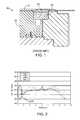
- FIG. 1shows a cross sectional view of a portion of a vacuum processing chamber having a hot edge ring and a quartz coupling ring.
- FIG. 2is a graph showing process drift for a plurality of wafers having a coupling ring and hot edge ring as set forth in arrangement of FIG. 1 .
- FIG. 3shows a cross sectional view of an edge ring assembly according to one embodiment.
- FIG. 4shows a cross sectional view of a portion of a vacuum processing chamber according to FIG. 3 at the location where the coupling ring is thermally coupled to the RF electrode via a conductive lower ring.
- FIG. 5is a graph showing process drift for a plurality of wafers having a intermediate ring and hot edge ring as set forth in arrangement of FIGS. 3 and 4 .
- FIG. 6is a graph showing process drift for a plurality of wafers comparing the hot edge ring of FIG. 1 versus the hot edge ring of FIGS. 3 and 4 .
- FIG. 7shows a cross sectional view of a plasma processing apparatus incorporating the edge ring assembly of FIGS. 3 and 4 .
- the hot edge ring assembly as disclosed hereinprovides a novel arrangement for improving uniformity and reducing etch rate drift at the edge of a wafer during plasma processing of semiconductor substrates such as wafers (e.g. silicon or gallium arsenide (GaAs)), flat panel display substrates, and the like.
- a temperature-controlled hot edge ring assemblycan achieve improved plasma processing.
- the temperature-controlled hot edge assemblyincreases the thermal contact between the upper ring having an exposed surface to the plasma processing chamber and a temperature controlled radio frequency (RF) electrode incorporated in a substrate support.
- RFradio frequency
- process uniformityrefers to the uniformity of the entire process, such as plasma etching across the surface of the substrate. If the process is highly uniform, for example, it is expected that the process rates at different points on the substrate tend to be substantially equal.
- wafer boundary conditionsare preferably designed for assuring continuity across the wafer in regard to the chemical exposure of the wafer edge, process pressure, and RF field strength.
- an edge ringhas been implemented fitting around the wafer.
- the edge ringis manufactured from a material compatible to the wafer itself.
- typical edge ring materialscan include silicon, graphite, silicon carbide or the like.
- the edge ringis resting on a ring made of quartz, (i.e., a quartz coupling ring), which is placed on the outer periphery of the RF electrode. Due to its low dielectric constant quartz is typically chosen for tapering the RF field strength at the edge of the wafer to enhance etch rate uniformity. On the other hand, quartz is also known to be a poor thermal conductor. As a result, an edge ring overlying a quartz coupling ring is thermally insulated. Thus, since the plasma is in the vicinity of the edge ring, the plasma heats the edge ring and may cause overheating of the edge ring and result in processing problems with the substrate or wafer.
- quartzi.e., a quartz coupling ring
- the edge ringUpon exposure to a heat source such as the RF plasma, the edge ring cannot cool adequately, which leads to a steady rise of its temperature. This temperature rise can lead to process drift (i.e., process non-uniformity) in etch rate at the edge of the wafer when multiple wafers are processed in close succession. Accordingly, since process drift can be caused by the steady increase in the temperature of the edge ring over the processing of multiple wafers, what is needed is a hot edge ring assembly, which allows improved cooling of the edge ring before the next substrate is processed and thereby reduces etch rate drift.
- process drifti.e., process non-uniformity
- the edge ring assemblymay be applied to plasma etching processes to enhance the density of a plasma near the edge of a wafer in a parallel plate plasma reaction chamber to produce a more uniform etch rate across the substrate.
- the hot edge ring assemblywill be described in terms of its advantages for plasma etching, the hot edge ring assembly is also useful for other applications that may require plasmas with uniform densities such as plasma enhanced chemical vapor deposition and plasma cleaning.
- the etch rate near the edge of the wafercan be controlled by modifying the quartz coupling ring and the edge ring to allow for sufficient cooling of the edge ring.
- the edge ring assemblyis heat sunk to the temperature controlled RF electrode.
- a thermally conductive elastomerbonds the edge ring to the coupling ring.
- the temperature of the edge ringrises due to the effects of the plasma. Depending on the RF power level and chamber pressure, the temperature rise can be significant and often exceed several dozen degrees Celsius.
- the waferis removed from the RF electrode and the next wafer is placed on the substrate support. If the edge ring temperature increases too much during a process run, wherein a batch of wafers undergoes sequential etching, the etch rate can drift outside the process window and result in defective wafers. It is desirable that before another wafer is added to the substrate support that the edge ring has sufficient heat sinking to allow the edge ring to return a temperature range as used for processing the previous wafer. However, this often does not occur, which leads to etch rate drift during the processing of a plurality of wafers.
- FIG. 1shows a cross-sectional view of a wafer edge region of a standard vacuum-processing chamber 10 .
- a substrate or waferis mounted on a substrate support 12 preferably incorporating an electrostatic chuck therein.
- the wafer edge ring assemblytypically includes an edge ring 20 and a coupling ring 30 .
- the edge ring 20can be bonded to the coupling ring 30 or can be resting flush on the coupling ring 30 .
- the vacuum-processing chamber 10also includes a radio frequency (RF) powered electrode 40 beneath the substrate support, which provides radio frequency energy to the substrate supported thereon.
- RFradio frequency
- a suitable RF impedance matching circuitcapacitively couples RF power into the chamber 10 via powered electrode 40 so as to provide high-density plasma.
- other plasma generating sourcescan be used (e.g., inductively-coupled coils, electron-cyclotron resonance (ECR), helicon or magnetron type).
- the chamber 10also includes a suitable vacuum pumping apparatus for maintaining the interior of the chamber at a desired pressure (e.g., at 50 mTorr, typically 30-1000 mTorr).
- a gas distribution platecommonly called a showerhead, may be provided and includes a plurality of openings such as circular holes (not shown) for delivering process gas supplied by a gas supply to the processing chamber 10 .
- the gas distribution platecan be omitted and process gas can be supplied to the chamber by other arrangements such as gas rings, etc.
- the rings surrounding the substrate supportincluding the hot edge ring 20 and the coupling ring 30 help focus the ions from the RF induced plasma region on the surface of the substrate to improve process uniformity, particularly at the edge of the substrate.
- equipotential field linesare set up over substrate and bottom electrode. These field lines are not static but change during the RF cycle. The time averaged field results in the bulk plasma being positive and the surface of the substrate and electrostatic chuck negative. Due to geometry factors, the field lines are not uniform at the edge of the substrate.
- the coupling, and hot edge ringshelp direct the bulk of the RF coupling through substrate to the overlying plasma by acting as a capacitor between the plasma and the powered electrode.
- the edge ring 20is a sacrificial ring surrounding the substrate support 12 .
- the edge ring 20is a replaceable component, which tends to become hot during processing of a substrate and thus is referred to as a hot edge ring (HER).
- the hot edge ring 20can be made from conductive electrode materials such as silicon carbide (SiC) and silicon (Si) or from dielectric materials such as quartz. It has been shown that, besides shifting the chemistry in the immediate neighborhood of the edge ring, by changing the edge ring material, the degree of coupling through the plasma can be tailored to provide a desired localized “edge” etch rate at the outer portion of a substrate being processed.
- Silicon carbide having a lower capacitive impedancewill generally produce a faster edge etch rate than silicon oxide. Quartz and other dielectrics with low dielectric constants will tend to lower the edge etch rate due to a reduction in RF coupling at the wafer edge.
- the coupling ring 30is made of a dielectric semi-conductive material such as quartz, silicon, silicon carbide, or aluminum oxide.
- FIG. 2is a graph showing the etch rate profile in a blanket oxide etch using a parallel plate arrangement with a dual frequency power supply.
- a run of seventeen (17) waferswas processed.
- a silicon edge ring 20 and quartz coupling ring 30were used and etching was carried out under the following conditions: 2000 Watts RF power at 27 MHz; 2000 Watts RF power at 2 MHz; 150 mTorr chamber pressure above the wafer; 400 sccm argon gas; 80 sccm C 4 F 8 gas; 8 sccm O 2 gas; and 60 second process time.
- the graphshows the Photoresist etch rate in Angstroms/minute as a function of location on the wafer surface measured from the center of the wafer. As can be seen from the graph, the etch rate at the edge of wafer varies substantially from wafer to wafer. Etch rate uniformity is calculated by the following equation: [(Max ⁇ Min)/2*Average]*100% where Max is the maximum value of etch rate and Min is the minimum value of etch rate. The etch rate was determined by measuring the thickness of the Photoresist layer on top of the wafer before and after etching using a commercially available thin-film metrology system.
- FIG. 3shows a cross section of a wafer edge region of a parallel plate plasma apparatus 100 having a temperature-controlled hot edge ring assembly 110 adapted to surround a substrate support according to one embodiment.
- the edge ring assembly 110includes an upper hot edge ring 120 , a ceramic intermediate ring 130 , and a conductive lower ring 140 .
- the intermediate ring 130has an upper surface 132 and a lower surface 134 , wherein the lower surface 134 of the intermediate ring 130 is thermally coupled to a radio frequency (RF) electrode 150 via the lower ring 140 .
- RFradio frequency
- the upper ring 120is preferably made of a thermally and electrically conductive material such as silicon, carbon (e.g., graphite), silicon carbide and the like. As shown in FIG. 3 , a lower surface 128 of the upper ring 120 is preferably bonded to an upper surface 132 of the intermediate ring 130 by a thermally conductive elastomer. Details of suitable elastomers are described in U.S. Pat. No. 6,073,577, which is hereby incorporated by reference.
- an inner portion of the upper surface 126 of the upper ring 120is beveled to form an angle with a plane perpendicular to the electrostatic chuck 112 .
- the beveled inner surface 126 of the upper ring 120allows a portion of the upper ring 120 to extend under the substrate when the substrate is located on the substrate support.
- the upper ring 120preferably has a substantially rectangular cross section, with the exception of the beveled inner surface 126 . It can be appreciated that the upper ring 120 can have other cross sectional designs or shapes.
- a dielectric outer ring 138can surround the upper ring 120 .
- the dielectric outer ring 138can be formed of aluminum oxide (Al 2 O 3 ), silicon oxide (quartz), silicon nitride, silicon carbide or other suitable materials and provides added protection to the plasma reactor chamber.
- the intermediate ring 130has a substantially rectangular cross-section and is preferably made of a material with high thermal conductivity and a similar thermal expansion coefficient as the material ring 120 is made of. If ring 120 is made out of silicon such materials may be aluminum oxide (ceramic), silicon, silicon carbide, or aluminum nitride. In one embodiment, the intermediate ring 130 is made of alumina. The intermediate ring 130 overlies the lower ring 140 and is preferably bolted to an RF electrode 150 via the lower ring 140 .
- the conductive lower ring 140is preferably made of a conductive material such as aluminum, aluminum alloy, brass, copper, copper alloy or stainless steel.
- the lower ring 140has a substantially L-shaped cross section and is made of aluminum.
- the lower ring 140can have a substantially rectangular cross section or other cross-sectional shape.
- FIG. 4is a cross section of the edge ring assembly 110 of FIG. 3 , wherein the intermediate ring 130 is bolted to the RF electrode 150 via the lower ring 140 .
- the bolting of the intermediate ring 130 to the RF electrode 150is preferably performed at a plurality of locations in the edge ring assembly 110 using a set of bolts (a first bolt 160 and a second bolt 170 ) extending through a plurality of holes in the lower ring 140 .
- the conductive lower ring 140is preferably L-shaped in cross section having a first plurality of holes 142 for bolting the lower ring 140 to the RF electrode 150 and a second plurality of threaded holes 144 for bolting the intermediate ring 130 to the lower ring 140 .
- the first plurality of holes 142is preferably located in the inner portion of the lower ring 140 whereas holes 144 are located at the outer portion of the lower ring 140 .
- the first plurality of holes 142has a taper 162 for receiving a taper head of the first bolt 160 .
- the bolt 160extends from the upper surface of the lower ring 140 through the lower ring 140 and into the RF electrode 150 .
- the bolt 160has a tapered head 162 at one end and a screw thread on the other end 164 .
- the RF electrode 150receives the screw thread 164 of the bolt 160 in a threaded hole 152 .
- the bolt 160is preferably stainless steel, however it can be appreciated that the first bolt can be aluminum, aluminum alloy, nickel, brass, copper, copper alloy or other suitable materials.
- the bolting of the intermediate ring 130 to the lower ring 140is preferably performed through a second plurality of holes 144 in the intermediate ring 130 .
- the second plurality of holes 144extend preferably into the outer portion of the lower ring 140 .
- the intermediate ring 130has a plurality of bolt receiving holes 133 for receiving a conductive washer 180 and a second bolt 170 .
- the bolt 170has a head 172 at one end and a screw thread 174 at the other.
- the conductive washer 180includes a counter-sunk hole 182 configured to receive the head 172 of the bolt 170 and the bolt 170 itself.
- the conductive washer 180preferably rests in the plurality of bolt receiving holes 133 .
- the conductive washer 180can be made of aluminum, aluminum alloy, nickel, brass, copper, copper alloy, stainless steel or any suitable material.
- the head 172 of the second bolt 170is positioned in the conductive washer 180 and extends through the intermediate ring 130 and into the lower ring 140 .
- the second bolt 170is also preferably stainless steel, however it can be appreciated that the bolt 170 can be aluminum, aluminum alloy, nickel, brass, copper, copper alloy or any suitable material.
- the upper ring 120has a plurality of holes 122 for receiving an edge ring cap 124 .
- the edge ring cap 124includes a vent hole 126 for venting of pressure in the edge ring assembly 110 .
- the edge ring cap 124preferably rests on a lip in hole 122 without touching the top of bolt 170 .
- the edge ring cap 124is preferably made of the same material as the upper ring 120 . Accordingly, the edge ring cap 124 can be made of silicon, graphite, silicon carbide and any other suitable material. Alternatively, the edge ring cap 124 can be made of quartz.
- the bolting of the lower ring 140 to the RF electrode 150is preferably performed at a plurality of locations in the edge ring assembly 110 .
- the number of holes 144 , 152is about 6 to 18 depending on the size of the edge ring assembly 110 .
- a plasma processing chamber for processing wafers having a diameter of 8 inches (200 mm)may have a different number of holes 144 , 152 , than a processed wafer having a diameter of 12 inches (300 mm).
- any number of first bolts 160 , second bolts 170 , and edge ring caps 124can be used to affix the edge ring assembly 110 to the RF electrode 150 .
- FIG. 5is a graph showing the effect of the hot edge ring 110 to the embodiment shown in FIGS. 3 and 4 .
- the same process conditions as shown in FIG. 2were used and were as follows: 2000 Watts RF power at 27 MHz; 2000 Watts RF power at 2 MHz; 150 mTorr chamber pressure above the wafer; 400 sccm argon gas; 80 sccm C 4 F 8 gas; 8 sccm O 2 gas; and 60 second process time.
- the temperature-controlled hot edge ring assembly 110greatly reduces the etch rate drift near the wafer edge.
- wafers number 1 , 2 , 5 and 17showed very little variance of etch rate at the outer portion of the wafer versus the results using the standard hot edge ring as shown in FIG. 1 resulting in a fairly large etch rate drift at the edge of the wafer as shown in FIG. 2 .
- FIG. 6graphs the etch rated at the edge of a wafer versus wafer number, comparing the standard quartz coupling ring as shown in FIG. 1 with the temperature controlled edge ring according to one embodiment and as shown in FIGS. 3 and 4 .
- the standard hot edge ringresulted in a considerable drop in etch rate for wafers number 1 - 5 , and a low etch rate for wafers 6 - 17
- the heat sunk hot edge ringresulted in a much higher etch rate which was substantially constant for the entire batch of wafers.
- the heat sunk hot edge ringeliminated the process drift in etch rate shown by the standard hot edge ring.
- temperature-controlled hot edge ring assembly 110can be installed in new vacuum processing chambers or used to retrofit existing vacuum processing chambers to provide adjustability of the upper ring 120 .
- the specific shape of the upper ring 120 , the intermediate ring 130 , and the lower ring 140may vary depending on the arrangement of chuck, substrate and/or others. Therefore, the exact shape of the rings surrounding the chuck in FIGS. 3 and 4 are shown for illustration purposes only and are not limiting in any way.
- FIG. 7shows a parallel plate plasma processing apparatus 200 incorporating the edge ring assembly 110 according to one embodiment.
- the plasma processing apparatus 200forms a processing chamber 210 having a top electrode 220 , and a temperature controlled lower electrode 150 incorporated in a substrate support 230 having an electrostatic chuck 240 for clamping the substrate S.
- the RF electrode 150energizes a process gas in the interior of the processing chamber 210 into a plasma state for processing a substrate S.
- An edge ring assembly 110including an upper ring 120 , a ceramic intermediate ring 130 and a conductive lower ring 140 as shown in FIGS. 3 and 4 surrounds the substrate support 240 .
- a preferred plasma reaction chamber incorporating the edge ring assembly 110is a semiconductor plasma etching apparatus.
- the temperature of the edge ring assembly 110is substantially cooled to an initial temperature after a first substrate is removed from the electrode and before a subsequent substrate is placed on the electrode.
- the edge ring assembly 110 incorporating the upper ring 120 , the ceramic intermediate ring 130 and the conductive lower ring 140provides an improved thermal path between the upper ring 120 and the temperature-controlled RF electrode 150 .
- the edge ring assembly 110can reduce process drift.
Landscapes
- Engineering & Computer Science (AREA)
- Physics & Mathematics (AREA)
- Condensed Matter Physics & Semiconductors (AREA)
- General Physics & Mathematics (AREA)
- Manufacturing & Machinery (AREA)
- Computer Hardware Design (AREA)
- Microelectronics & Electronic Packaging (AREA)
- Power Engineering (AREA)
- Plasma & Fusion (AREA)
- Chemical & Material Sciences (AREA)
- Analytical Chemistry (AREA)
- Drying Of Semiconductors (AREA)
Abstract
Description
- Since the mid-1960s, integrated semiconductor circuits have become the primary components of most electronics systems. These miniature electronic devices may contain thousands of the transistors and other circuits that make up the memory and logic subsystems of microcomputer central processing units and other integrated circuits. The low cost, high reliability, and speed of these chips have led them to become a ubiquitous feature of modem digital electronics.
- The fabrication of an integrated circuit chip typically begins with a thin, polished slice of high-purity, single-crystal semiconductor material substrate (such as silicon or germanium) called a “wafer.” Each wafer is subjected to a sequence of physical and chemical processing steps that form the various circuit structures on the wafer. During the fabrication process, various types of thin films may be deposited on the wafer using various techniques such as thermal oxidation to produce silicon dioxide films, chemical vapor deposition to produce silicon, silicon dioxide, and silicon nitride films, and sputtering or other techniques to produce other metal films.
- After depositing a film on the semiconductor wafer, the unique electrical properties of semiconductors are produced by substituting selected impurities into the semiconductor crystal lattice using a process called doping. The doped silicon wafer may then be uniformly coated with a thin layer of photosensitive, or radiation sensitive material, called a “resist.” Small geometric patterns defining the electron paths in the circuit may then be transferred onto the resist using a process known as lithography. During the lithographic process, the integrated circuit pattern may be drawn on a glass plate called a “mask” and then optically reduced, projected, and transferred onto the photosensitive coating.
- The lithographed resist pattern is then transferred onto the underlying crystalline surface of the semiconductor material through a process known as etching. Vacuum processing chambers are generally used for etching and chemical vapor deposition (CVD) of materials on substrates by supplying an etching or deposition gas to the vacuum chamber and application of a radio frequency (RF) field to the gas to energize the gas into a plasma state. However, in plasma processing of wafers, process drift (i.e., the change of process performance over a certain amount of time) can occur. Accordingly, there is a need for apparatuses and methods for improving etch rate uniformity in plasma reactor processing.
- In accordance with one embodiment, a temperature-controlled hot edge ring assembly adapted to surround a substrate support in a plasma reaction chamber includes a conductive lower ring; a ceramic intermediate ring, the intermediate ring overlying the lower ring, the intermediate ring adapted to be attached via the lower ring to an RF electrode; and an upper ring, the upper ring overlying the intermediate ring, wherein the upper ring has an upper surface exposed to an interior of a plasma reaction chamber.
- In accordance with another embodiment, a plasma processing apparatus includes a processing chamber; a power source which energizes process gas in an interior of the processing chamber into a plasma state for processing a substrate; a substrate support which supports a substrate within the interior of the processing chamber; a conductive lower ring; a ceramic intermediate ring, the intermediate ring overlying the lower ring, the intermediate ring adapted to be attached via the lower ring to an RF electrode; and an upper ring, the upper ring overlying the intermediate ring, wherein the upper ring has an upper surface exposed to an interior of a plasma reaction chamber.
- In accordance with a further embodiment, a method of reducing process drift on a plurality of substrates in a plasma processing system, the method including the steps of: positioning a substrate in a plasma processing apparatus comprising: a processing chamber; a power source which energizes process gas in an interior of the processing chamber into a plasma state for processing a substrate; a substrate support which supports a substrate within the interior of the processing chamber, the substrate support having an upper surface; and an edge ring assembly comprising: a conductive lower ring; a ceramic intermediate ring, the intermediate ring overlying the lower ring, the intermediate ring adapted to be attached via the lower ring to the power source; and an upper ring, the upper ring overlying the intermediate ring, wherein the upper ring has an upper surface exposed to an interior of the processing chamber; supplying process gas to the chamber; forming a plasma adjacent the upper surface of the substrate support; and sequentially processing a plurality of substrates in the plasma processing apparatus, wherein the temperature of the upper ring is substantially cooled to an initial temperature after a first substrate is removed from the substrate support and before a subsequent substrate is placed on the substrate support to reduce process drift.
FIG. 1 shows a cross sectional view of a portion of a vacuum processing chamber having a hot edge ring and a quartz coupling ring.FIG. 2 is a graph showing process drift for a plurality of wafers having a coupling ring and hot edge ring as set forth in arrangement ofFIG. 1 .FIG. 3 shows a cross sectional view of an edge ring assembly according to one embodiment.FIG. 4 shows a cross sectional view of a portion of a vacuum processing chamber according toFIG. 3 at the location where the coupling ring is thermally coupled to the RF electrode via a conductive lower ring.FIG. 5 is a graph showing process drift for a plurality of wafers having a intermediate ring and hot edge ring as set forth in arrangement ofFIGS. 3 and 4 .FIG. 6 is a graph showing process drift for a plurality of wafers comparing the hot edge ring ofFIG. 1 versus the hot edge ring ofFIGS. 3 and 4 .FIG. 7 shows a cross sectional view of a plasma processing apparatus incorporating the edge ring assembly ofFIGS. 3 and 4 .- The hot edge ring assembly as disclosed herein provides a novel arrangement for improving uniformity and reducing etch rate drift at the edge of a wafer during plasma processing of semiconductor substrates such as wafers (e.g. silicon or gallium arsenide (GaAs)), flat panel display substrates, and the like. A temperature-controlled hot edge ring assembly can achieve improved plasma processing. The temperature-controlled hot edge assembly increases the thermal contact between the upper ring having an exposed surface to the plasma processing chamber and a temperature controlled radio frequency (RF) electrode incorporated in a substrate support. Thus, by increasing the thermal contact, the hot edge ring assembly can reduce processing etch rate drift.
- In processing substrates, process engineers strive to improve process uniformity. As the term is employed herein, process uniformity refers to the uniformity of the entire process, such as plasma etching across the surface of the substrate. If the process is highly uniform, for example, it is expected that the process rates at different points on the substrate tend to be substantially equal.
- For control of etch rate uniformity on a semiconductor substrates, such as a wafer, in particular, for matching the etch rate at the center of the wafer to the rate at the wafer edge, wafer boundary conditions are preferably designed for assuring continuity across the wafer in regard to the chemical exposure of the wafer edge, process pressure, and RF field strength. In the current designs, an edge ring has been implemented fitting around the wafer. In order to minimize wafer contamination, the edge ring is manufactured from a material compatible to the wafer itself. As an example, typical edge ring materials can include silicon, graphite, silicon carbide or the like.
- Typically, the edge ring is resting on a ring made of quartz, (i.e., a quartz coupling ring), which is placed on the outer periphery of the RF electrode. Due to its low dielectric constant quartz is typically chosen for tapering the RF field strength at the edge of the wafer to enhance etch rate uniformity. On the other hand, quartz is also known to be a poor thermal conductor. As a result, an edge ring overlying a quartz coupling ring is thermally insulated. Thus, since the plasma is in the vicinity of the edge ring, the plasma heats the edge ring and may cause overheating of the edge ring and result in processing problems with the substrate or wafer. Upon exposure to a heat source such as the RF plasma, the edge ring cannot cool adequately, which leads to a steady rise of its temperature. This temperature rise can lead to process drift (i.e., process non-uniformity) in etch rate at the edge of the wafer when multiple wafers are processed in close succession. Accordingly, since process drift can be caused by the steady increase in the temperature of the edge ring over the processing of multiple wafers, what is needed is a hot edge ring assembly, which allows improved cooling of the edge ring before the next substrate is processed and thereby reduces etch rate drift.
- The edge ring assembly may be applied to plasma etching processes to enhance the density of a plasma near the edge of a wafer in a parallel plate plasma reaction chamber to produce a more uniform etch rate across the substrate. Although the hot edge ring assembly will be described in terms of its advantages for plasma etching, the hot edge ring assembly is also useful for other applications that may require plasmas with uniform densities such as plasma enhanced chemical vapor deposition and plasma cleaning.
- The etch rate near the edge of the wafer can be controlled by modifying the quartz coupling ring and the edge ring to allow for sufficient cooling of the edge ring. According to a preferred embodiment, the edge ring assembly is heat sunk to the temperature controlled RF electrode. In one embodiment, a thermally conductive elastomer bonds the edge ring to the coupling ring.
- Typically, during the plasma etching process, the temperature of the edge ring rises due to the effects of the plasma. Depending on the RF power level and chamber pressure, the temperature rise can be significant and often exceed several dozen degrees Celsius. After the plasma etching-processing step is finished, the wafer is removed from the RF electrode and the next wafer is placed on the substrate support. If the edge ring temperature increases too much during a process run, wherein a batch of wafers undergoes sequential etching, the etch rate can drift outside the process window and result in defective wafers. It is desirable that before another wafer is added to the substrate support that the edge ring has sufficient heat sinking to allow the edge ring to return a temperature range as used for processing the previous wafer. However, this often does not occur, which leads to etch rate drift during the processing of a plurality of wafers.
FIG. 1 shows a cross-sectional view of a wafer edge region of a standard vacuum-processing chamber 10. As shown inFIG. 1 , a substrate or wafer is mounted on asubstrate support 12 preferably incorporating an electrostatic chuck therein. The wafer edge ring assembly typically includes anedge ring 20 and acoupling ring 30. Theedge ring 20 can be bonded to thecoupling ring 30 or can be resting flush on thecoupling ring 30. The vacuum-processing chamber 10 also includes a radio frequency (RF) poweredelectrode 40 beneath the substrate support, which provides radio frequency energy to the substrate supported thereon.- A suitable RF impedance matching circuit capacitively couples RF power into the
chamber 10 via poweredelectrode 40 so as to provide high-density plasma. If desired, other plasma generating sources can be used (e.g., inductively-coupled coils, electron-cyclotron resonance (ECR), helicon or magnetron type). Thechamber 10 also includes a suitable vacuum pumping apparatus for maintaining the interior of the chamber at a desired pressure (e.g., at 50 mTorr, typically 30-1000 mTorr). A gas distribution plate, commonly called a showerhead, may be provided and includes a plurality of openings such as circular holes (not shown) for delivering process gas supplied by a gas supply to theprocessing chamber 10. However, the gas distribution plate can be omitted and process gas can be supplied to the chamber by other arrangements such as gas rings, etc. - As is well known to those familiar with the plasma processing art, the rings surrounding the substrate support, including the
hot edge ring 20 and thecoupling ring 30 help focus the ions from the RF induced plasma region on the surface of the substrate to improve process uniformity, particularly at the edge of the substrate. When power is supplied to the substrate and electrostatic chuck, equipotential field lines are set up over substrate and bottom electrode. These field lines are not static but change during the RF cycle. The time averaged field results in the bulk plasma being positive and the surface of the substrate and electrostatic chuck negative. Due to geometry factors, the field lines are not uniform at the edge of the substrate. In the plasma chamber, the coupling, and hot edge rings help direct the bulk of the RF coupling through substrate to the overlying plasma by acting as a capacitor between the plasma and the powered electrode. - As shown in
FIG. 1 , theedge ring 20 is a sacrificial ring surrounding thesubstrate support 12. Theedge ring 20 is a replaceable component, which tends to become hot during processing of a substrate and thus is referred to as a hot edge ring (HER). Thehot edge ring 20 can be made from conductive electrode materials such as silicon carbide (SiC) and silicon (Si) or from dielectric materials such as quartz. It has been shown that, besides shifting the chemistry in the immediate neighborhood of the edge ring, by changing the edge ring material, the degree of coupling through the plasma can be tailored to provide a desired localized “edge” etch rate at the outer portion of a substrate being processed. Silicon carbide having a lower capacitive impedance, will generally produce a faster edge etch rate than silicon oxide. Quartz and other dielectrics with low dielectric constants will tend to lower the edge etch rate due to a reduction in RF coupling at the wafer edge. Typically, thecoupling ring 30 is made of a dielectric semi-conductive material such as quartz, silicon, silicon carbide, or aluminum oxide. FIG. 2 is a graph showing the etch rate profile in a blanket oxide etch using a parallel plate arrangement with a dual frequency power supply. A run of seventeen (17) wafers was processed. Asilicon edge ring 20 andquartz coupling ring 30 were used and etching was carried out under the following conditions: 2000 Watts RF power at 27 MHz; 2000 Watts RF power at 2 MHz; 150 mTorr chamber pressure above the wafer; 400 sccm argon gas; 80 sccm C4F8gas; 8 sccm O2gas; and 60 second process time.- The graph shows the Photoresist etch rate in Angstroms/minute as a function of location on the wafer surface measured from the center of the wafer. As can be seen from the graph, the etch rate at the edge of wafer varies substantially from wafer to wafer. Etch rate uniformity is calculated by the following equation:
[(Max−Min)/2*Average]*100%
where Max is the maximum value of etch rate and Min is the minimum value of etch rate. The etch rate was determined by measuring the thickness of the Photoresist layer on top of the wafer before and after etching using a commercially available thin-film metrology system. FIG. 3 shows a cross section of a wafer edge region of a parallelplate plasma apparatus 100 having a temperature-controlled hotedge ring assembly 110 adapted to surround a substrate support according to one embodiment. Theedge ring assembly 110 includes an upperhot edge ring 120, a ceramicintermediate ring 130, and a conductivelower ring 140. Theintermediate ring 130 has anupper surface 132 and alower surface 134, wherein thelower surface 134 of theintermediate ring 130 is thermally coupled to a radio frequency (RF)electrode 150 via thelower ring 140.- The
upper ring 120 is preferably made of a thermally and electrically conductive material such as silicon, carbon (e.g., graphite), silicon carbide and the like. As shown inFIG. 3 , alower surface 128 of theupper ring 120 is preferably bonded to anupper surface 132 of theintermediate ring 130 by a thermally conductive elastomer. Details of suitable elastomers are described in U.S. Pat. No. 6,073,577, which is hereby incorporated by reference. - In one embodiment, an inner portion of the
upper surface 126 of theupper ring 120 is beveled to form an angle with a plane perpendicular to theelectrostatic chuck 112. The beveledinner surface 126 of theupper ring 120 allows a portion of theupper ring 120 to extend under the substrate when the substrate is located on the substrate support. Theupper ring 120 preferably has a substantially rectangular cross section, with the exception of the beveledinner surface 126. It can be appreciated that theupper ring 120 can have other cross sectional designs or shapes. - If desirable, a dielectric
outer ring 138 can surround theupper ring 120. The dielectricouter ring 138 can be formed of aluminum oxide (Al2O3), silicon oxide (quartz), silicon nitride, silicon carbide or other suitable materials and provides added protection to the plasma reactor chamber. - The
intermediate ring 130 has a substantially rectangular cross-section and is preferably made of a material with high thermal conductivity and a similar thermal expansion coefficient as thematerial ring 120 is made of. Ifring 120 is made out of silicon such materials may be aluminum oxide (ceramic), silicon, silicon carbide, or aluminum nitride. In one embodiment, theintermediate ring 130 is made of alumina. Theintermediate ring 130 overlies thelower ring 140 and is preferably bolted to anRF electrode 150 via thelower ring 140. - The conductive
lower ring 140 is preferably made of a conductive material such as aluminum, aluminum alloy, brass, copper, copper alloy or stainless steel. In one embodiment, thelower ring 140 has a substantially L-shaped cross section and is made of aluminum. However, it can be appreciated that thelower ring 140 can have a substantially rectangular cross section or other cross-sectional shape. FIG. 4 is a cross section of theedge ring assembly 110 ofFIG. 3 , wherein theintermediate ring 130 is bolted to theRF electrode 150 via thelower ring 140. The bolting of theintermediate ring 130 to theRF electrode 150 is preferably performed at a plurality of locations in theedge ring assembly 110 using a set of bolts (afirst bolt 160 and a second bolt170) extending through a plurality of holes in thelower ring 140.- As shown in
FIGS. 3 and 4 , the conductivelower ring 140 is preferably L-shaped in cross section having a first plurality ofholes 142 for bolting thelower ring 140 to theRF electrode 150 and a second plurality of threadedholes 144 for bolting theintermediate ring 130 to thelower ring 140. The first plurality ofholes 142 is preferably located in the inner portion of thelower ring 140 whereasholes 144 are located at the outer portion of thelower ring 140. - In one embodiment, the first plurality of
holes 142 has ataper 162 for receiving a taper head of thefirst bolt 160. Thebolt 160 extends from the upper surface of thelower ring 140 through thelower ring 140 and into theRF electrode 150. Preferably, thebolt 160 has a taperedhead 162 at one end and a screw thread on theother end 164. TheRF electrode 150 receives thescrew thread 164 of thebolt 160 in a threadedhole 152. Thebolt 160 is preferably stainless steel, however it can be appreciated that the first bolt can be aluminum, aluminum alloy, nickel, brass, copper, copper alloy or other suitable materials. - The bolting of the
intermediate ring 130 to thelower ring 140 is preferably performed through a second plurality ofholes 144 in theintermediate ring 130. The second plurality ofholes 144 extend preferably into the outer portion of thelower ring 140. In one embodiment, theintermediate ring 130 has a plurality ofbolt receiving holes 133 for receiving aconductive washer 180 and asecond bolt 170. Thebolt 170 has ahead 172 at one end and ascrew thread 174 at the other. Theconductive washer 180 includes acounter-sunk hole 182 configured to receive thehead 172 of thebolt 170 and thebolt 170 itself. Theconductive washer 180 preferably rests in the plurality ofbolt receiving holes 133. In addition, it can be appreciated that theconductive washer 180 can be made of aluminum, aluminum alloy, nickel, brass, copper, copper alloy, stainless steel or any suitable material. - The
head 172 of thesecond bolt 170 is positioned in theconductive washer 180 and extends through theintermediate ring 130 and into thelower ring 140. Thesecond bolt 170 is also preferably stainless steel, however it can be appreciated that thebolt 170 can be aluminum, aluminum alloy, nickel, brass, copper, copper alloy or any suitable material. - As shown in
FIG. 4 , theupper ring 120 has a plurality ofholes 122 for receiving anedge ring cap 124. Theedge ring cap 124 includes avent hole 126 for venting of pressure in theedge ring assembly 110. Theedge ring cap 124 preferably rests on a lip inhole 122 without touching the top ofbolt 170. Theedge ring cap 124 is preferably made of the same material as theupper ring 120. Accordingly, theedge ring cap 124 can be made of silicon, graphite, silicon carbide and any other suitable material. Alternatively, theedge ring cap 124 can be made of quartz. - Since, the
edge ring assembly 110 surrounds a substrate in a plasma reactor, the bolting of thelower ring 140 to theRF electrode 150 is preferably performed at a plurality of locations in theedge ring assembly 110. In one embodiment, the number ofholes edge ring assembly 110. For example, a plasma processing chamber for processing wafers having a diameter of 8 inches (200 mm) may have a different number ofholes first bolts 160,second bolts 170, and edge ring caps124 can be used to affix theedge ring assembly 110 to theRF electrode 150. FIG. 5 is a graph showing the effect of thehot edge ring 110 to the embodiment shown inFIGS. 3 and 4 . The same process conditions as shown inFIG. 2 were used and were as follows: 2000 Watts RF power at 27 MHz; 2000 Watts RF power at 2 MHz; 150 mTorr chamber pressure above the wafer; 400 sccm argon gas; 80 sccm C4F8gas; 8 sccm O2gas; and 60 second process time.- As shown in
FIG. 5 , the temperature-controlled hotedge ring assembly 110 greatly reduces the etch rate drift near the wafer edge. During a process run of a cassette of wafers,wafers number FIG. 1 resulting in a fairly large etch rate drift at the edge of the wafer as shown inFIG. 2 . FIG. 6 graphs the etch rated at the edge of a wafer versus wafer number, comparing the standard quartz coupling ring as shown inFIG. 1 with the temperature controlled edge ring according to one embodiment and as shown inFIGS. 3 and 4 . Whereas the standard hot edge ring resulted in a considerable drop in etch rate for wafers number1-5, and a low etch rate for wafers6-17, the heat sunk hot edge ring resulted in a much higher etch rate which was substantially constant for the entire batch of wafers. Thus, the heat sunk hot edge ring eliminated the process drift in etch rate shown by the standard hot edge ring.- It can be appreciated that the temperature-controlled hot
edge ring assembly 110 can be installed in new vacuum processing chambers or used to retrofit existing vacuum processing chambers to provide adjustability of theupper ring 120. - It should be appreciated that in a specific system, the specific shape of the
upper ring 120, theintermediate ring 130, and thelower ring 140 may vary depending on the arrangement of chuck, substrate and/or others. Therefore, the exact shape of the rings surrounding the chuck inFIGS. 3 and 4 are shown for illustration purposes only and are not limiting in any way. FIG. 7 shows a parallel plateplasma processing apparatus 200 incorporating theedge ring assembly 110 according to one embodiment. Theplasma processing apparatus 200 forms aprocessing chamber 210 having atop electrode 220, and a temperature controlledlower electrode 150 incorporated in asubstrate support 230 having anelectrostatic chuck 240 for clamping the substrate S. TheRF electrode 150 energizes a process gas in the interior of theprocessing chamber 210 into a plasma state for processing a substrate S. Anedge ring assembly 110, including anupper ring 120, a ceramicintermediate ring 130 and a conductivelower ring 140 as shown inFIGS. 3 and 4 surrounds thesubstrate support 240. A preferred plasma reaction chamber incorporating theedge ring assembly 110 is a semiconductor plasma etching apparatus.- In operation, when sequentially processing a plurality of substrates in the
plasma processing apparatus 200, the temperature of theedge ring assembly 110 is substantially cooled to an initial temperature after a first substrate is removed from the electrode and before a subsequent substrate is placed on the electrode. As shown inFIGS. 3, 4 and7, theedge ring assembly 110 incorporating theupper ring 120, the ceramicintermediate ring 130 and the conductivelower ring 140 provides an improved thermal path between theupper ring 120 and the temperature-controlledRF electrode 150. Thus, it can be appreciated that by cooling theedge ring assembly 110 to its initial temperature, theedge ring assembly 110 can reduce process drift. - Although the present invention has been described in connection with preferred embodiments thereof, it will be appreciated by those skilled in the art that additions, deletions, modifications, and substitutions not specifically described can be made without departing from the spirit and scope of the invention as defined in the appended claims.
Claims (24)
1. A temperature-controlled hot edge ring assembly adapted to surround a semiconductor substrate support in a plasma reaction chamber, the assembly comprising:
a conductive lower ring;
a ceramic intermediate ring, the intermediate ring overlying the lower ring, the intermediate ring adapted to be attached via the lower ring to an RF electrode; and
an upper ring, the upper ring overlying the intermediate ring, wherein the upper ring has an upper surface exposed to an interior of a plasma reaction chamber.
2. The assembly ofclaim 1 , wherein the intermediate ring is made of aluminum oxide.
3. The assembly ofclaim 1 , wherein the intermediate ring is made of quartz, silicon, silicon carbide or aluminum oxide.
4. The assembly ofclaim 1 , wherein the conductive ring is made of aluminum or alloy thereof.
5. The assembly ofclaim 1 , wherein the conductive ring is made of aluminum, aluminum alloy, brass, copper, copper alloy or stainless steel.
6. The assembly ofclaim 1 , wherein a lower surface of the upper ring is bonded to an upper surface of the intermediate ring via a thermally conductive elastomer.
7. The assembly ofclaim 1 , wherein the conductive ring has a plurality of holes configured to bolt the conductive ring to the RF electrode.
8. The assembly ofclaim 1 , wherein the conductive ring and the intermediate ring have a plurality of holes configured to bolt the intermediate ring to the conductive ring.
9. The assembly ofclaim 1 , wherein the conductive ring has a substantially L-shaped cross-section.
10. The assembly ofclaim 7 , further comprising a first bolt having a tapered head at one end and a screw thread at the other end, the first bolt configured to bolt the conductive ring to the RF electrode.
11. The assembly ofclaim 8 , further comprising a second bolt having a head at one end and a screw thread at the other end, the second bolt configured to bolt the intermediate ring to the conductive ring.
12. The assembly ofclaim 1 , further comprising a conductive washer configured to receive a bolt having a head at one end and a screw thread at the other end, wherein the conductive washer is positioned between the upper ring and the intermediate ring.
13. The assembly ofclaim 12 , further comprising a plurality of holes in the upper ring, wherein the plurality of holes receive a cap, the cap having a vent hole configured to release pressure from within the edge ring assembly.
14. The assembly ofclaim 1 , wherein the upper ring is made of silicon, carbon, graphite, or silicon carbide.
15. The assembly ofclaim 1 , wherein the upper ring has a portion extending under a substrate when the substrate is located on the substrate support.
16. A plasma processing apparatus comprising:
a processing chamber;
a power source which energizes process gas in an interior of the processing chamber into a plasma state for processing a substrate;
a substrate support which supports a substrate within the interior of the processing chamber;
a conductive lower ring;
a ceramic intermediate ring, the intermediate ring overlying the lower ring, the intermediate ring adapted to be attached via the lower ring to an RF electrode; and
an upper ring, the upper ring overlying the intermediate ring, wherein the upper ring has an upper surface exposed to an interior of a plasma reaction chamber.
17. The apparatus ofclaim 16 , wherein the upper ring is bonded to the intermediate ring by a thermally conductive elastomer.
18. The apparatus ofclaim 16 , wherein the lower ring is made of aluminum or alloy thereof.
19. The apparatus ofclaim 16 , wherein the intermediate ring is made of aluminum oxide.
20. The apparatus ofclaim 16 , wherein the upper ring is made from a material selected from the group consisting of quartz, silicon, silicon carbide, graphite and aluminum.
21. The apparatus ofclaim 16 , wherein the plasma chamber is a semiconductor plasma etching apparatus.
22. The apparatus ofclaim 16 , further comprising a quartz outer ring surrounding the upper ring, the intermediate ring, the lower ring and the RF electrode.
23. A method of reducing process drift on a plurality of substrates in a plasma processing system comprising:
positioning a substrate in a plasma processing apparatus comprising:
a processing chamber;
a power source which energizes process gas in an interior of the processing chamber into a plasma state for processing a substrate;
a substrate support which supports a substrate within the interior of the processing chamber, the substrate support having an upper surface; and
an edge ring assembly comprising:
a conductive lower ring;
a ceramic intermediate ring, the intermediate ring overlying the lower ring, the intermediate ring adapted to be attached via the lower ring to the power source; and
an upper ring, the upper ring overlying the intermediate ring, wherein the upper ring has an upper surface exposed to an interior of the processing chamber;
supplying process gas to the chamber;
forming a plasma adjacent the upper surface of the substrate support; and
sequentially processing a plurality of substrates in the plasma processing apparatus, wherein the temperature of the upper ring is substantially cooled to an initial temperature after a first substrate is removed from the substrate support and before a subsequent substrate is placed on the substrate support to reduce process drift.
24. The method ofclaim 23 , wherein the substrate comprises a semiconductor wafer and the processing step comprises etching the semiconductor wafer with the plasma.
Priority Applications (7)
| Application Number | Priority Date | Filing Date | Title |
|---|---|---|---|
| US10/736,666US7244336B2 (en) | 2003-12-17 | 2003-12-17 | Temperature controlled hot edge ring assembly for reducing plasma reactor etch rate drift |
| EP04818010.3AEP1706898B1 (en) | 2003-12-17 | 2004-12-10 | Temperature controlled hot edge ring assembly for reducing plasma reactor etch rate drift |
| CNB2004800414213ACN100474521C (en) | 2003-12-17 | 2004-12-10 | Temperature controlled hot edge ring assembly, and device comprising the same and the use thereof |
| PCT/US2004/041768WO2005059962A2 (en) | 2003-12-17 | 2004-12-10 | Temperature controlled hot edge ring assembly for reducing plasma reactor etch rate drift |
| KR1020067014066AKR101131022B1 (en) | 2003-12-17 | 2004-12-10 | Temperature controlled hot edge ring assembly for reducing plasma reactor etch rate drift |
| JP2006545785AJP4913603B2 (en) | 2003-12-17 | 2004-12-10 | Temperature controlled hot edge ring assembly for reducing etch rate drift in plasma reactors |
| TW093139170ATWI368274B (en) | 2003-12-17 | 2004-12-16 | Temperature controlled hot edge ring assembly, plasma processing apparatus and method of reducing process drift in a plasma processing system |
Applications Claiming Priority (1)
| Application Number | Priority Date | Filing Date | Title |
|---|---|---|---|
| US10/736,666US7244336B2 (en) | 2003-12-17 | 2003-12-17 | Temperature controlled hot edge ring assembly for reducing plasma reactor etch rate drift |
Publications (2)
| Publication Number | Publication Date |
|---|---|
| US20050133164A1true US20050133164A1 (en) | 2005-06-23 |
| US7244336B2 US7244336B2 (en) | 2007-07-17 |
Family
ID=34677226
Family Applications (1)
| Application Number | Title | Priority Date | Filing Date |
|---|---|---|---|
| US10/736,666Expired - LifetimeUS7244336B2 (en) | 2003-12-17 | 2003-12-17 | Temperature controlled hot edge ring assembly for reducing plasma reactor etch rate drift |
Country Status (7)
| Country | Link |
|---|---|
| US (1) | US7244336B2 (en) |
| EP (1) | EP1706898B1 (en) |
| JP (1) | JP4913603B2 (en) |
| KR (1) | KR101131022B1 (en) |
| CN (1) | CN100474521C (en) |
| TW (1) | TWI368274B (en) |
| WO (1) | WO2005059962A2 (en) |
Cited By (82)
| Publication number | Priority date | Publication date | Assignee | Title |
|---|---|---|---|---|
| US20030130683A1 (en)* | 2001-12-03 | 2003-07-10 | Xtent, Inc., | Apparatus and methods for delivering coiled prostheses |
| US20040098081A1 (en)* | 2001-12-03 | 2004-05-20 | Xtent, Inc. | Apparatus and methods for deployment of vascular prostheses |
| US20040134618A1 (en)* | 2003-01-07 | 2004-07-15 | Tokyo Electron Limited | Plasma processing apparatus and focus ring |
| US20040215312A1 (en)* | 2001-12-03 | 2004-10-28 | Xtent, Inc. | Stent delivery apparatus and method |
| US20050017540A1 (en)* | 2003-07-22 | 2005-01-27 | Leigh Arthur Donald | Caravan |
| US20050274321A1 (en)* | 2004-06-10 | 2005-12-15 | Tokyo Electron Limited | Plasma processing apparatus and method |
| US20050288763A1 (en)* | 2004-06-28 | 2005-12-29 | Xtent, Inc. | Custom-length self-expanding stent delivery systems with stent bumpers |
| US20060000805A1 (en)* | 2004-06-30 | 2006-01-05 | Applied Materials, Inc. | Method and apparatus for stable plasma processing |
| US20060000802A1 (en)* | 2004-06-30 | 2006-01-05 | Ajay Kumar | Method and apparatus for photomask plasma etching |
| US20070018265A1 (en)* | 2005-07-20 | 2007-01-25 | Seiko Epson Corporation | Mask, mask manufacturing method, film forming method, electro-optic device manufacturing method, and electronic apparatus |
| US20070100424A1 (en)* | 2001-12-03 | 2007-05-03 | Xtent, Inc. | Apparatus and methods for delivery of multiple distributed stents |
| US7294146B2 (en) | 2001-12-03 | 2007-11-13 | Xtent, Inc. | Apparatus and methods for delivery of variable length stents |
| US7326236B2 (en) | 2003-12-23 | 2008-02-05 | Xtent, Inc. | Devices and methods for controlling and indicating the length of an interventional element |
| US7357812B2 (en) | 2001-12-03 | 2008-04-15 | Xtent, Inc. | Apparatus and methods for delivery of braided prostheses |
| US20080097574A1 (en)* | 2003-10-15 | 2008-04-24 | Xtent, Inc. | Implantable stent delivery devices and methods |
| US20080099426A1 (en)* | 2006-10-30 | 2008-05-01 | Ajay Kumar | Method and apparatus for photomask plasma etching |
| US20080099431A1 (en)* | 2006-10-30 | 2008-05-01 | Applied Materials, Inc. | Method and apparatus for photomask plasma etching |
| US20080099448A1 (en)* | 2006-10-16 | 2008-05-01 | Lam Research Corporation | Quartz guard ring |
| US7402168B2 (en) | 2005-04-11 | 2008-07-22 | Xtent, Inc. | Custom-length stent delivery system with independently operable expansion elements |
| US20080194113A1 (en)* | 2006-09-20 | 2008-08-14 | Samsung Electronics Co., Ltd. | Methods and apparatus for semiconductor etching including an electro static chuck |
| KR100858599B1 (en)* | 2006-02-21 | 2008-09-17 | 가부시키가이샤 뉴플레어 테크놀로지 | Vapor phase deposition apparatus and support table |
| US20080241420A1 (en)* | 2007-03-30 | 2008-10-02 | Rajinder Dhindsa | Method and apparatus for dc voltage control on rf-powered electrode |
| US20080289766A1 (en)* | 2007-05-22 | 2008-11-27 | Samsung Austin Semiconductor Lp | Hot edge ring apparatus and method for increased etch rate uniformity and reduced polymer buildup |
| US20090000744A1 (en)* | 2007-06-28 | 2009-01-01 | Rajinder Dhindsa | Edge ring arrangements for substrate processing |
| US7553324B2 (en) | 2003-10-14 | 2009-06-30 | Xtent, Inc. | Fixed stent delivery devices and methods |
| US20100040768A1 (en)* | 2008-08-15 | 2010-02-18 | Lam Research Corporation | Temperature controlled hot edge ring assembly |
| US20100065216A1 (en)* | 2006-05-30 | 2010-03-18 | Applied Materials, Inc. | Ring assembly for substrate processing chamber |
| US20100078899A1 (en)* | 2008-09-26 | 2010-04-01 | Lam Research Corporation | Adjustable thermal contact between an electrostatic chuck and a hot edge ring by clocking a coupling ring |
| US20100159703A1 (en)* | 2008-12-19 | 2010-06-24 | Andreas Fischer | Methods and apparatus for dual confinement and ultra-high pressure in an adjustable gap plasma chamber |
| US20110022148A1 (en)* | 2007-02-20 | 2011-01-27 | Xtent, Inc. | Thermo-mechanically controlled implants and methods of use |
| US7922755B2 (en) | 2001-12-03 | 2011-04-12 | Xtent, Inc. | Apparatus and methods for delivery of multiple distributed stents |
| US20110104884A1 (en)* | 2009-11-02 | 2011-05-05 | Lam Research Corporation | Hot edge ring with sloped upper surface |
| US8080048B2 (en) | 2001-12-03 | 2011-12-20 | Xtent, Inc. | Stent delivery for bifurcated vessels |
| US20120055403A1 (en)* | 2009-03-03 | 2012-03-08 | Tokyo Electron Limited | Mounting table structure, film forming apparatus and raw material recovery method |
| CN102569109A (en)* | 2011-07-07 | 2012-07-11 | 杨继远 | Method for enlarging bonding area of chip |
| US8486132B2 (en) | 2007-03-22 | 2013-07-16 | J.W. Medical Systems Ltd. | Devices and methods for controlling expandable prostheses during deployment |
| US8652198B2 (en) | 2006-03-20 | 2014-02-18 | J.W. Medical Systems Ltd. | Apparatus and methods for deployment of linked prosthetic segments |
| US20140065835A1 (en)* | 2008-02-08 | 2014-03-06 | Lam Research Corporation | Protective coating for a plasma processing chamber part and a method of use |
| US8769796B2 (en) | 2008-09-25 | 2014-07-08 | Advanced Bifurcation Systems, Inc. | Selective stent crimping |
| US8795347B2 (en) | 2008-09-25 | 2014-08-05 | Advanced Bifurcation Systems, Inc. | Methods and systems for treating a bifurcation with provisional side branch stenting |
| US8808347B2 (en) | 2008-09-25 | 2014-08-19 | Advanced Bifurcation Systems, Inc. | Stent alignment during treatment of a bifurcation |
| US8821562B2 (en) | 2008-09-25 | 2014-09-02 | Advanced Bifurcation Systems, Inc. | Partially crimped stent |
| WO2014209489A1 (en)* | 2013-06-28 | 2014-12-31 | Applied Materials, Inc. | Process kit for edge critical dimension uniformity control |
| US8956398B2 (en) | 2001-12-03 | 2015-02-17 | J.W. Medical Systems Ltd. | Custom length stent apparatus |
| US8979917B2 (en) | 2008-09-25 | 2015-03-17 | Advanced Bifurcation Systems, Inc. | System and methods for treating a bifurcation |
| US9101503B2 (en) | 2008-03-06 | 2015-08-11 | J.W. Medical Systems Ltd. | Apparatus having variable strut length and methods of use |
| US9254210B2 (en) | 2011-02-08 | 2016-02-09 | Advanced Bifurcation Systems, Inc. | Multi-stent and multi-balloon apparatus for treating bifurcations and methods of use |
| US9364356B2 (en) | 2011-02-08 | 2016-06-14 | Advanced Bifurcation System, Inc. | System and methods for treating a bifurcation with a fully crimped stent |
| WO2016099826A1 (en)* | 2014-12-19 | 2016-06-23 | Applied Materials, Inc. | Edge ring for a substrate processing chamber |
| US20170002465A1 (en)* | 2015-06-30 | 2017-01-05 | Lam Research Corporation | Separation of Plasma Suppression and Wafer Edge to Improve Edge Film Thickness Uniformity |
| US20170011892A1 (en)* | 2014-02-24 | 2017-01-12 | Beijing Nmc Co., Ltd. | Bearing device and plasma processing apparatus |
| US20170162422A1 (en)* | 2015-12-07 | 2017-06-08 | Applied Materials, Inc. | Amalgamated cover ring |
| US9700448B2 (en) | 2004-06-28 | 2017-07-11 | J.W. Medical Systems Ltd. | Devices and methods for controlling expandable prostheses during deployment |
| US20170213758A1 (en)* | 2016-01-26 | 2017-07-27 | Applied Materials, Inc. | Wafer edge ring lifting solution |
| US10504702B2 (en) | 2016-12-16 | 2019-12-10 | Applied Materials, Inc. | Adjustable extended electrode for edge uniformity control |
| US10512125B2 (en)* | 2015-01-06 | 2019-12-17 | Tokyo Electron Limited | Mounting table and substrate processing apparatus |
| US10553404B2 (en) | 2017-02-01 | 2020-02-04 | Applied Materials, Inc. | Adjustable extended electrode for edge uniformity control |
| US10600623B2 (en) | 2018-05-28 | 2020-03-24 | Applied Materials, Inc. | Process kit with adjustable tuning ring for edge uniformity control |
| US20200118787A1 (en)* | 2018-10-10 | 2020-04-16 | Tokyo Electron Limited | Substrate support assembly, plasma processing apparatus, and plasma processing method |
| CN111755312A (en)* | 2019-03-29 | 2020-10-09 | 东京毅力科创株式会社 | Plasma processing apparatus |
| US11000392B2 (en) | 2008-09-25 | 2021-05-11 | Advanced Bifurcation Systems Inc. | Partially crimped stent |
| US11043400B2 (en) | 2017-12-21 | 2021-06-22 | Applied Materials, Inc. | Movable and removable process kit |
| US11075105B2 (en) | 2017-09-21 | 2021-07-27 | Applied Materials, Inc. | In-situ apparatus for semiconductor process module |
| WO2021158612A1 (en)* | 2020-02-04 | 2021-08-12 | Lam Research Corporation | Electrostatic edge ring mounting system for substrate processing |
| US11101115B2 (en) | 2019-04-19 | 2021-08-24 | Applied Materials, Inc. | Ring removal from processing chamber |
| US11211282B2 (en)* | 2018-06-15 | 2021-12-28 | Applied Materials, Inc. | Apparatus to reduce contamination in a plasma etching chamber |
| US11289310B2 (en) | 2018-11-21 | 2022-03-29 | Applied Materials, Inc. | Circuits for edge ring control in shaped DC pulsed plasma process device |
| US11298252B2 (en) | 2008-09-25 | 2022-04-12 | Advanced Bifurcation Systems Inc. | Stent alignment during treatment of a bifurcation |
| US20220293453A1 (en)* | 2021-03-12 | 2022-09-15 | Applied Materials, Inc. | Multi-zone semiconductor substrate supports |
| US20220344134A1 (en)* | 2018-01-19 | 2022-10-27 | Applied Materials, Inc. | Process kit for a substrate support |
| WO2022252296A1 (en)* | 2021-06-03 | 2022-12-08 | 长鑫存储技术有限公司 | Semiconductor etching device |
| US20230145476A1 (en)* | 2021-11-09 | 2023-05-11 | Samsung Electronics Co., Ltd. | Chuck assembly, fabrication system therewith, and method of fabricating semiconductor device using the same |
| US20240060182A1 (en)* | 2022-08-17 | 2024-02-22 | Sky Tech Inc. | Wafer carrier with adjustable alignment devices and deposition equipment using the same |
| US11935773B2 (en) | 2018-06-14 | 2024-03-19 | Applied Materials, Inc. | Calibration jig and calibration method |
| US20240102153A1 (en)* | 2022-09-27 | 2024-03-28 | Applied Materials, Inc. | Protective gas flow during wafer dechucking in pvd chamber |
| US11984304B2 (en) | 2021-04-12 | 2024-05-14 | Samsung Electronics Co., Ltd. | Apparatus and method for plasma etching |
| US12009236B2 (en) | 2019-04-22 | 2024-06-11 | Applied Materials, Inc. | Sensors and system for in-situ edge ring erosion monitor |
| US12076258B2 (en) | 2008-09-25 | 2024-09-03 | Advanced Bifurcation Systems Inc. | Selective stent crimping |
| US12094752B2 (en) | 2016-01-26 | 2024-09-17 | Applied Materials, Inc. | Wafer edge ring lifting solution |
| WO2025010122A1 (en)* | 2023-07-06 | 2025-01-09 | Applied Materials, Inc. | Shield ring mounting using compliant hardware |
| US12324756B2 (en) | 2008-09-25 | 2025-06-10 | Advanced Bifurcation Systems Inc. | System and methods for treating a bifurcation |
| US12444579B2 (en) | 2020-03-23 | 2025-10-14 | Lam Research Corporation | Mid-ring erosion compensation in substrate processing systems |
Families Citing this family (37)
| Publication number | Priority date | Publication date | Assignee | Title |
|---|---|---|---|---|
| TWI246873B (en)* | 2001-07-10 | 2006-01-01 | Tokyo Electron Ltd | Plasma processing device |
| GB0121980D0 (en) | 2001-09-11 | 2001-10-31 | Cathnet Science Holding As | Expandable stent |
| US20040186551A1 (en) | 2003-01-17 | 2004-09-23 | Xtent, Inc. | Multiple independent nested stent structures and methods for their preparation and deployment |
| US7182779B2 (en) | 2001-12-03 | 2007-02-27 | Xtent, Inc. | Apparatus and methods for positioning prostheses for deployment from a catheter |
| US7241308B2 (en) | 2003-06-09 | 2007-07-10 | Xtent, Inc. | Stent deployment systems and methods |
| US7658816B2 (en)* | 2003-09-05 | 2010-02-09 | Tokyo Electron Limited | Focus ring and plasma processing apparatus |
| US7323006B2 (en) | 2004-03-30 | 2008-01-29 | Xtent, Inc. | Rapid exchange interventional devices and methods |
| JP2005303099A (en)* | 2004-04-14 | 2005-10-27 | Hitachi High-Technologies Corp | Plasma processing apparatus and plasma processing method |
| JP2008078208A (en)* | 2006-09-19 | 2008-04-03 | Tokyo Electron Ltd | Focus ring and plasma processing apparatus |
| JP5035884B2 (en) | 2007-03-27 | 2012-09-26 | 東京エレクトロン株式会社 | Thermal conductive sheet and substrate mounting apparatus using the same |
| US7884925B2 (en)* | 2008-05-23 | 2011-02-08 | Lam Research Corporation | Electrical and optical system and methods for monitoring erosion of electrostatic chuck edge bead materials |
| US20100116788A1 (en)* | 2008-11-12 | 2010-05-13 | Lam Research Corporation | Substrate temperature control by using liquid controlled multizone substrate support |
| KR101559913B1 (en)* | 2009-06-25 | 2015-10-27 | 삼성전자주식회사 | Plasma dry etching apparatus |
| DE202010015933U1 (en)* | 2009-12-01 | 2011-03-31 | Lam Research Corp.(N.D.Ges.D.Staates Delaware), Fremont | An edge ring arrangement for plasma etching chambers |
| JP2011176228A (en)* | 2010-02-25 | 2011-09-08 | Oki Semiconductor Co Ltd | Plasma processing apparatus and focus ring |
| US9947559B2 (en)* | 2011-10-28 | 2018-04-17 | Applied Materials, Inc. | Thermal management of edge ring in semiconductor processing |
| CN103094037B (en)* | 2011-11-08 | 2016-04-20 | 北京北方微电子基地设备工艺研究中心有限责任公司 | A kind of clamping device and apply the plasma processing device of this clamping device |
| US9412579B2 (en)* | 2012-04-26 | 2016-08-09 | Applied Materials, Inc. | Methods and apparatus for controlling substrate uniformity |
| US9449797B2 (en) | 2013-05-07 | 2016-09-20 | Lam Research Corporation | Component of a plasma processing apparatus having a protective in situ formed layer on a plasma exposed surface |
| TWI491758B (en) | 2013-05-14 | 2015-07-11 | Global Material Science Co Ltd | Deposition apparatus for photoelectrical semiconductor manufacturing process and shadow frame thereof |
| US10804081B2 (en)* | 2013-12-20 | 2020-10-13 | Lam Research Corporation | Edge ring dimensioned to extend lifetime of elastomer seal in a plasma processing chamber |
| US9633875B2 (en)* | 2015-03-13 | 2017-04-25 | Varian Semiconductor Equipment Associates, Inc. | Apparatus for improving temperature uniformity of a workpiece |
| KR101729124B1 (en) | 2015-10-16 | 2017-04-24 | 세메스 주식회사 | Apparatus and method for treating a substrate with support unit |
| US20180122670A1 (en)* | 2016-11-01 | 2018-05-03 | Varian Semiconductor Equipment Associates, Inc. | Removable substrate plane structure ring |
| KR102581226B1 (en) | 2016-12-23 | 2023-09-20 | 삼성전자주식회사 | Plasma processing device |
| TWI780093B (en)* | 2017-12-15 | 2022-10-11 | 美商蘭姆研究公司 | Ring structures and systems for use in a plasma chamber |
| WO2019117969A1 (en)* | 2017-12-15 | 2019-06-20 | Lam Research Corporation | Ring structures and systems for use in a plasma chamber |
| KR102647177B1 (en) | 2019-02-11 | 2024-03-15 | 삼성전자주식회사 | Plasma processing apparatus |
| KR102702089B1 (en)* | 2019-03-22 | 2024-09-03 | 삼성전자주식회사 | Substrate processing apparatus including edge ring |
| US11894255B2 (en) | 2019-07-30 | 2024-02-06 | Applied Materials, Inc. | Sheath and temperature control of process kit |
| JP2021040011A (en)* | 2019-09-02 | 2021-03-11 | キオクシア株式会社 | Plasma processing apparatus |
| JP7471810B2 (en)* | 2019-12-13 | 2024-04-22 | 東京エレクトロン株式会社 | Ring assembly, substrate support and substrate processing apparatus - Patents.com |
| KR20220102201A (en) | 2021-01-12 | 2022-07-20 | 삼성전자주식회사 | chuck assembly, manufacturing apparatus of semiconductor device including the same and manufacturing method of semiconductor device |
| JP2022150471A (en)* | 2021-03-26 | 2022-10-07 | 三菱電機株式会社 | Semiconductor manufacturing device and method for manufacturing semiconductor device |
| CN120565385A (en)* | 2021-09-08 | 2025-08-29 | 北京屹唐半导体科技股份有限公司 | Conductive member for cleaning focus ring of plasma processing equipment |
| JP7569772B2 (en)* | 2021-10-07 | 2024-10-18 | 日本碍子株式会社 | Semiconductor manufacturing equipment parts |
| KR102722858B1 (en)* | 2022-07-29 | 2024-10-29 | 하나머티리얼즈(주) | Focus Ring and method for manufacturing the same |
Citations (13)
| Publication number | Priority date | Publication date | Assignee | Title |
|---|---|---|---|---|
| US6073577A (en)* | 1998-06-30 | 2000-06-13 | Lam Research Corporation | Electrode for plasma processes and method for manufacture and use thereof |
| US6159299A (en)* | 1999-02-09 | 2000-12-12 | Applied Materials, Inc. | Wafer pedestal with a purge ring |
| US6238513B1 (en)* | 1999-12-28 | 2001-05-29 | International Business Machines Corporation | Wafer lift assembly |
| US6251215B1 (en)* | 1998-06-03 | 2001-06-26 | Applied Materials, Inc. | Carrier head with a multilayer retaining ring for chemical mechanical polishing |
| US6277008B1 (en)* | 1998-04-10 | 2001-08-21 | Nec Corporation | Polishing apparatus |
| US6344105B1 (en)* | 1999-06-30 | 2002-02-05 | Lam Research Corporation | Techniques for improving etch rate uniformity |
| US6363882B1 (en)* | 1999-12-30 | 2002-04-02 | Lam Research Corporation | Lower electrode design for higher uniformity |
| US6383931B1 (en)* | 2000-02-11 | 2002-05-07 | Lam Research Corporation | Convertible hot edge ring to improve low-K dielectric etch |
| US6391787B1 (en)* | 2000-10-13 | 2002-05-21 | Lam Research Corporation | Stepped upper electrode for plasma processing uniformity |
| US6475336B1 (en)* | 2000-10-06 | 2002-11-05 | Lam Research Corporation | Electrostatically clamped edge ring for plasma processing |
| US6567258B2 (en)* | 1999-12-22 | 2003-05-20 | Lam Research Corporation | High temperature electrostatic chuck |
| US6589352B1 (en)* | 1999-12-10 | 2003-07-08 | Applied Materials, Inc. | Self aligning non contact shadow ring process kit |
| US6896765B2 (en)* | 2002-09-18 | 2005-05-24 | Lam Research Corporation | Method and apparatus for the compensation of edge ring wear in a plasma processing chamber |
Family Cites Families (11)
| Publication number | Priority date | Publication date | Assignee | Title |
|---|---|---|---|---|
| JPH03150365A (en)* | 1989-07-26 | 1991-06-26 | Tokyo Electron Ltd | Heat treating device |
| JPH04279044A (en)* | 1991-01-09 | 1992-10-05 | Sumitomo Metal Ind Ltd | Sample holding device |
| JP3209472B2 (en)* | 1993-11-05 | 2001-09-17 | 東京エレクトロン株式会社 | Screw cap and processing equipment |
| US6048403A (en)* | 1998-04-01 | 2000-04-11 | Applied Materials, Inc. | Multi-ledge substrate support for a thermal processing chamber |
| US6379491B1 (en)* | 1998-10-30 | 2002-04-30 | Promos Technologies, Inc. | Plasma chamber with erosion resistive securement screws |
| JP2001093877A (en)* | 1999-09-22 | 2001-04-06 | Texas Instr Japan Ltd | Method for manufacturing semiconductor device |
| KR100635975B1 (en)* | 2000-02-14 | 2006-10-20 | 동경 엘렉트론 주식회사 | Apparatus and method for plasma treatment |
| JP4592916B2 (en)* | 2000-04-25 | 2010-12-08 | 東京エレクトロン株式会社 | Placement device for workpiece |
| TW506234B (en)* | 2000-09-18 | 2002-10-11 | Tokyo Electron Ltd | Tunable focus ring for plasma processing |
| JP4877884B2 (en)* | 2001-01-25 | 2012-02-15 | 東京エレクトロン株式会社 | Plasma processing equipment |
| US6554954B2 (en)* | 2001-04-03 | 2003-04-29 | Applied Materials Inc. | Conductive collar surrounding semiconductor workpiece in plasma chamber |
- 2003
- 2003-12-17USUS10/736,666patent/US7244336B2/ennot_activeExpired - Lifetime
- 2004
- 2004-12-10KRKR1020067014066Apatent/KR101131022B1/ennot_activeExpired - Lifetime
- 2004-12-10EPEP04818010.3Apatent/EP1706898B1/ennot_activeExpired - Lifetime
- 2004-12-10JPJP2006545785Apatent/JP4913603B2/ennot_activeExpired - Lifetime
- 2004-12-10WOPCT/US2004/041768patent/WO2005059962A2/enactiveApplication Filing
- 2004-12-10CNCNB2004800414213Apatent/CN100474521C/ennot_activeExpired - Lifetime
- 2004-12-16TWTW093139170Apatent/TWI368274B/ennot_activeIP Right Cessation
Patent Citations (13)
| Publication number | Priority date | Publication date | Assignee | Title |
|---|---|---|---|---|
| US6277008B1 (en)* | 1998-04-10 | 2001-08-21 | Nec Corporation | Polishing apparatus |
| US6251215B1 (en)* | 1998-06-03 | 2001-06-26 | Applied Materials, Inc. | Carrier head with a multilayer retaining ring for chemical mechanical polishing |
| US6073577A (en)* | 1998-06-30 | 2000-06-13 | Lam Research Corporation | Electrode for plasma processes and method for manufacture and use thereof |
| US6159299A (en)* | 1999-02-09 | 2000-12-12 | Applied Materials, Inc. | Wafer pedestal with a purge ring |
| US6344105B1 (en)* | 1999-06-30 | 2002-02-05 | Lam Research Corporation | Techniques for improving etch rate uniformity |
| US6589352B1 (en)* | 1999-12-10 | 2003-07-08 | Applied Materials, Inc. | Self aligning non contact shadow ring process kit |
| US6567258B2 (en)* | 1999-12-22 | 2003-05-20 | Lam Research Corporation | High temperature electrostatic chuck |
| US6238513B1 (en)* | 1999-12-28 | 2001-05-29 | International Business Machines Corporation | Wafer lift assembly |
| US6363882B1 (en)* | 1999-12-30 | 2002-04-02 | Lam Research Corporation | Lower electrode design for higher uniformity |
| US6383931B1 (en)* | 2000-02-11 | 2002-05-07 | Lam Research Corporation | Convertible hot edge ring to improve low-K dielectric etch |
| US6475336B1 (en)* | 2000-10-06 | 2002-11-05 | Lam Research Corporation | Electrostatically clamped edge ring for plasma processing |
| US6391787B1 (en)* | 2000-10-13 | 2002-05-21 | Lam Research Corporation | Stepped upper electrode for plasma processing uniformity |
| US6896765B2 (en)* | 2002-09-18 | 2005-05-24 | Lam Research Corporation | Method and apparatus for the compensation of edge ring wear in a plasma processing chamber |
Cited By (166)
| Publication number | Priority date | Publication date | Assignee | Title |
|---|---|---|---|---|
| US7309350B2 (en) | 2001-12-03 | 2007-12-18 | Xtent, Inc. | Apparatus and methods for deployment of vascular prostheses |
| US7905913B2 (en) | 2001-12-03 | 2011-03-15 | Xtent, Inc. | Apparatus and methods for delivery of multiple distributed stents |
| US7922755B2 (en) | 2001-12-03 | 2011-04-12 | Xtent, Inc. | Apparatus and methods for delivery of multiple distributed stents |
| US20040215312A1 (en)* | 2001-12-03 | 2004-10-28 | Xtent, Inc. | Stent delivery apparatus and method |
| US7892274B2 (en) | 2001-12-03 | 2011-02-22 | Xtent, Inc. | Apparatus and methods for deployment of vascular prostheses |
| US7357812B2 (en) | 2001-12-03 | 2008-04-15 | Xtent, Inc. | Apparatus and methods for delivery of braided prostheses |
| US8956398B2 (en) | 2001-12-03 | 2015-02-17 | J.W. Medical Systems Ltd. | Custom length stent apparatus |
| US7270668B2 (en) | 2001-12-03 | 2007-09-18 | Xtent, Inc. | Apparatus and methods for delivering coiled prostheses |
| US20070156226A1 (en)* | 2001-12-03 | 2007-07-05 | Xtent, Inc. | Apparatus and methods for delivery of multiple distributed stents |
| US7351255B2 (en) | 2001-12-03 | 2008-04-01 | Xtent, Inc. | Stent delivery apparatus and method |
| US20040098081A1 (en)* | 2001-12-03 | 2004-05-20 | Xtent, Inc. | Apparatus and methods for deployment of vascular prostheses |
| US20070100424A1 (en)* | 2001-12-03 | 2007-05-03 | Xtent, Inc. | Apparatus and methods for delivery of multiple distributed stents |
| US8080048B2 (en) | 2001-12-03 | 2011-12-20 | Xtent, Inc. | Stent delivery for bifurcated vessels |
| US7294146B2 (en) | 2001-12-03 | 2007-11-13 | Xtent, Inc. | Apparatus and methods for delivery of variable length stents |
| US20030130683A1 (en)* | 2001-12-03 | 2003-07-10 | Xtent, Inc., | Apparatus and methods for delivering coiled prostheses |
| US9326876B2 (en) | 2001-12-03 | 2016-05-03 | J.W. Medical Systems Ltd. | Apparatus and methods for delivery of multiple distributed stents |
| US7850174B2 (en)* | 2003-01-07 | 2010-12-14 | Tokyo Electron Limited | Plasma processing apparatus and focus ring |
| US20110048643A1 (en)* | 2003-01-07 | 2011-03-03 | Tokyo Electon Limited | Plasma processing apparatus and focus ring |
| US20040134618A1 (en)* | 2003-01-07 | 2004-07-15 | Tokyo Electron Limited | Plasma processing apparatus and focus ring |
| US8114247B2 (en) | 2003-01-07 | 2012-02-14 | Tokyo Electron Limited | Plasma processing apparatus and focus ring |
| US20050017540A1 (en)* | 2003-07-22 | 2005-01-27 | Leigh Arthur Donald | Caravan |
| US7553324B2 (en) | 2003-10-14 | 2009-06-30 | Xtent, Inc. | Fixed stent delivery devices and methods |
| US20080097574A1 (en)* | 2003-10-15 | 2008-04-24 | Xtent, Inc. | Implantable stent delivery devices and methods |
| US7326236B2 (en) | 2003-12-23 | 2008-02-05 | Xtent, Inc. | Devices and methods for controlling and indicating the length of an interventional element |
| US9566179B2 (en) | 2003-12-23 | 2017-02-14 | J.W. Medical Systems Ltd. | Devices and methods for controlling and indicating the length of an interventional element |
| US7713431B2 (en)* | 2004-06-10 | 2010-05-11 | Tokyo Electron Limited | Plasma processing method |
| US20050274321A1 (en)* | 2004-06-10 | 2005-12-15 | Tokyo Electron Limited | Plasma processing apparatus and method |
| US9700448B2 (en) | 2004-06-28 | 2017-07-11 | J.W. Medical Systems Ltd. | Devices and methods for controlling expandable prostheses during deployment |
| US20090234428A1 (en)* | 2004-06-28 | 2009-09-17 | Xtent, Inc. | Devices and methods for controlling expandable prostheses during deployment |
| US7300456B2 (en) | 2004-06-28 | 2007-11-27 | Xtent, Inc. | Custom-length self-expanding stent delivery systems with stent bumpers |
| US20050288763A1 (en)* | 2004-06-28 | 2005-12-29 | Xtent, Inc. | Custom-length self-expanding stent delivery systems with stent bumpers |
| US8986362B2 (en) | 2004-06-28 | 2015-03-24 | J.W. Medical Systems Ltd. | Devices and methods for controlling expandable prostheses during deployment |
| US8801896B2 (en) | 2004-06-30 | 2014-08-12 | Applied Materials, Inc. | Method and apparatus for stable plasma processing |
| US8349128B2 (en) | 2004-06-30 | 2013-01-08 | Applied Materials, Inc. | Method and apparatus for stable plasma processing |
| US20060000805A1 (en)* | 2004-06-30 | 2006-01-05 | Applied Materials, Inc. | Method and apparatus for stable plasma processing |
| US20060000802A1 (en)* | 2004-06-30 | 2006-01-05 | Ajay Kumar | Method and apparatus for photomask plasma etching |
| US7402168B2 (en) | 2005-04-11 | 2008-07-22 | Xtent, Inc. | Custom-length stent delivery system with independently operable expansion elements |
| US7909932B2 (en)* | 2005-07-20 | 2011-03-22 | Seiko Epson Corporation | Mask, mask manufacturing method, film forming method, electro-optic device manufacturing method, and electronic apparatus |
| US20070018265A1 (en)* | 2005-07-20 | 2007-01-25 | Seiko Epson Corporation | Mask, mask manufacturing method, film forming method, electro-optic device manufacturing method, and electronic apparatus |
| KR100858599B1 (en)* | 2006-02-21 | 2008-09-17 | 가부시키가이샤 뉴플레어 테크놀로지 | Vapor phase deposition apparatus and support table |
| US8652198B2 (en) | 2006-03-20 | 2014-02-18 | J.W. Medical Systems Ltd. | Apparatus and methods for deployment of linked prosthetic segments |
| US9883957B2 (en) | 2006-03-20 | 2018-02-06 | J.W. Medical Systems Ltd. | Apparatus and methods for deployment of linked prosthetic segments |
| US20100065216A1 (en)* | 2006-05-30 | 2010-03-18 | Applied Materials, Inc. | Ring assembly for substrate processing chamber |
| US20080194113A1 (en)* | 2006-09-20 | 2008-08-14 | Samsung Electronics Co., Ltd. | Methods and apparatus for semiconductor etching including an electro static chuck |
| US20080099448A1 (en)* | 2006-10-16 | 2008-05-01 | Lam Research Corporation | Quartz guard ring |
| US20090127234A1 (en)* | 2006-10-16 | 2009-05-21 | Lam Research Corporation | Plasma processing chamber with guard ring for upper electrode assembly |
| US7482550B2 (en)* | 2006-10-16 | 2009-01-27 | Lam Research Corporation | Quartz guard ring |
| US7939778B2 (en) | 2006-10-16 | 2011-05-10 | Lam Research Corporation | Plasma processing chamber with guard ring for upper electrode assembly |
| US7943005B2 (en) | 2006-10-30 | 2011-05-17 | Applied Materials, Inc. | Method and apparatus for photomask plasma etching |
| US8568553B2 (en) | 2006-10-30 | 2013-10-29 | Applied Materials, Inc. | Method and apparatus for photomask plasma etching |
| US20080099431A1 (en)* | 2006-10-30 | 2008-05-01 | Applied Materials, Inc. | Method and apparatus for photomask plasma etching |
| US20080099426A1 (en)* | 2006-10-30 | 2008-05-01 | Ajay Kumar | Method and apparatus for photomask plasma etching |
| US7909961B2 (en) | 2006-10-30 | 2011-03-22 | Applied Materials, Inc. | Method and apparatus for photomask plasma etching |
| US9457133B2 (en) | 2007-02-20 | 2016-10-04 | J.W. Medical Systems Ltd. | Thermo-mechanically controlled implants and methods of use |
| US20110022148A1 (en)* | 2007-02-20 | 2011-01-27 | Xtent, Inc. | Thermo-mechanically controlled implants and methods of use |
| US8980297B2 (en) | 2007-02-20 | 2015-03-17 | J.W. Medical Systems Ltd. | Thermo-mechanically controlled implants and methods of use |
| US8486132B2 (en) | 2007-03-22 | 2013-07-16 | J.W. Medical Systems Ltd. | Devices and methods for controlling expandable prostheses during deployment |
| US9339404B2 (en) | 2007-03-22 | 2016-05-17 | J.W. Medical Systems Ltd. | Devices and methods for controlling expandable prostheses during deployment |
| US9536711B2 (en)* | 2007-03-30 | 2017-01-03 | Lam Research Corporation | Method and apparatus for DC voltage control on RF-powered electrode |
| TWI451468B (en)* | 2007-03-30 | 2014-09-01 | Lam Res Corp | Method for processing a substrate |
| US20080241420A1 (en)* | 2007-03-30 | 2008-10-02 | Rajinder Dhindsa | Method and apparatus for dc voltage control on rf-powered electrode |
| US20080289766A1 (en)* | 2007-05-22 | 2008-11-27 | Samsung Austin Semiconductor Lp | Hot edge ring apparatus and method for increased etch rate uniformity and reduced polymer buildup |
| US7837827B2 (en)* | 2007-06-28 | 2010-11-23 | Lam Research Corporation | Edge ring arrangements for substrate processing |
| US20110070743A1 (en)* | 2007-06-28 | 2011-03-24 | Rajinder Dhindsa | Apparatus and methods for edge ring implementation for substrate processing |
| US20090000744A1 (en)* | 2007-06-28 | 2009-01-01 | Rajinder Dhindsa | Edge ring arrangements for substrate processing |
| US9184074B2 (en) | 2007-06-28 | 2015-11-10 | Lam Research Corporation | Apparatus and methods for edge ring implementation for substrate processing |
| US20140065835A1 (en)* | 2008-02-08 | 2014-03-06 | Lam Research Corporation | Protective coating for a plasma processing chamber part and a method of use |
| US9101503B2 (en) | 2008-03-06 | 2015-08-11 | J.W. Medical Systems Ltd. | Apparatus having variable strut length and methods of use |
| US20100040768A1 (en)* | 2008-08-15 | 2010-02-18 | Lam Research Corporation | Temperature controlled hot edge ring assembly |
| WO2010019196A3 (en)* | 2008-08-15 | 2010-04-15 | Lam Research Corporation | Temperature controlled hot edge ring assembly |
| US8449679B2 (en)* | 2008-08-15 | 2013-05-28 | Lam Research Corporation | Temperature controlled hot edge ring assembly |
| US10610391B2 (en) | 2008-09-25 | 2020-04-07 | Advanced Bifurcation Systems Inc. | Stent alignment during treatment of a bifurcation |
| US9855158B2 (en) | 2008-09-25 | 2018-01-02 | Advanced Bifurcation Systems, Inc. | Stent alignment during treatment of a bifurcation |
| US10918506B2 (en) | 2008-09-25 | 2021-02-16 | Advanced Bifurcation Systems Inc. | System and methods for treating a bifurcation |
| US11000392B2 (en) | 2008-09-25 | 2021-05-11 | Advanced Bifurcation Systems Inc. | Partially crimped stent |
| US8979917B2 (en) | 2008-09-25 | 2015-03-17 | Advanced Bifurcation Systems, Inc. | System and methods for treating a bifurcation |
| US8795347B2 (en) | 2008-09-25 | 2014-08-05 | Advanced Bifurcation Systems, Inc. | Methods and systems for treating a bifurcation with provisional side branch stenting |
| US10219927B2 (en) | 2008-09-25 | 2019-03-05 | Advanced Bifurcation Systems Inc. | System and methods for treating a bifurcation |
| US10219926B2 (en) | 2008-09-25 | 2019-03-05 | Advanced Bifurcation Systems Inc. | Selective stent crimping |
| US8828071B2 (en) | 2008-09-25 | 2014-09-09 | Advanced Bifurcation Systems, Inc. | Methods and systems for ostial stenting of a bifurcation |
| US8769796B2 (en) | 2008-09-25 | 2014-07-08 | Advanced Bifurcation Systems, Inc. | Selective stent crimping |
| US12042412B2 (en) | 2008-09-25 | 2024-07-23 | Advanced Bifurcation Systems Inc. | Stent alignment during treatment of a bifurcation |
| US12076258B2 (en) | 2008-09-25 | 2024-09-03 | Advanced Bifurcation Systems Inc. | Selective stent crimping |
| US8808347B2 (en) | 2008-09-25 | 2014-08-19 | Advanced Bifurcation Systems, Inc. | Stent alignment during treatment of a bifurcation |
| US9724218B2 (en) | 2008-09-25 | 2017-08-08 | Advanced Bifurcation Systems, Inc. | Methods and systems for ostial stenting of a bifurcation |
| US11857442B2 (en) | 2008-09-25 | 2024-01-02 | Advanced Bifurcation Systems Inc. | System and methods for treating a bifurcation |
| US11839562B2 (en) | 2008-09-25 | 2023-12-12 | Advanced Bifurcation Systems Inc. | Partially crimped stent |
| US8821562B2 (en) | 2008-09-25 | 2014-09-02 | Advanced Bifurcation Systems, Inc. | Partially crimped stent |
| US12324756B2 (en) | 2008-09-25 | 2025-06-10 | Advanced Bifurcation Systems Inc. | System and methods for treating a bifurcation |
| US11426297B2 (en) | 2008-09-25 | 2022-08-30 | Advanced Bifurcation Systems Inc. | Selective stent crimping |
| US11298252B2 (en) | 2008-09-25 | 2022-04-12 | Advanced Bifurcation Systems Inc. | Stent alignment during treatment of a bifurcation |
| US9730821B2 (en) | 2008-09-25 | 2017-08-15 | Advanced Bifurcation Systems, Inc. | Methods and systems for treating a bifurcation with provisional side branch stenting |
| US8454027B2 (en)* | 2008-09-26 | 2013-06-04 | Lam Research Corporation | Adjustable thermal contact between an electrostatic chuck and a hot edge ring by clocking a coupling ring |
| US20100078899A1 (en)* | 2008-09-26 | 2010-04-01 | Lam Research Corporation | Adjustable thermal contact between an electrostatic chuck and a hot edge ring by clocking a coupling ring |
| US20100159703A1 (en)* | 2008-12-19 | 2010-06-24 | Andreas Fischer | Methods and apparatus for dual confinement and ultra-high pressure in an adjustable gap plasma chamber |
| US9548186B2 (en)* | 2008-12-19 | 2017-01-17 | Lam Research Corporation | Methods and apparatus for dual confinement and ultra-high pressure in an adjustable gap plasma chamber |
| US20150011097A1 (en)* | 2008-12-19 | 2015-01-08 | Lam Research Corporation | Methods and apparatus for dual confinement and ultra-high pressure in an adjustable gap plasma chamber |
| US8869741B2 (en)* | 2008-12-19 | 2014-10-28 | Lam Research Corporation | Methods and apparatus for dual confinement and ultra-high pressure in an adjustable gap plasma chamber |
| US20120055403A1 (en)* | 2009-03-03 | 2012-03-08 | Tokyo Electron Limited | Mounting table structure, film forming apparatus and raw material recovery method |
| US8992686B2 (en)* | 2009-03-03 | 2015-03-31 | Tokyo Electron Limited | Mounting table structure, film forming apparatus and raw material recovery method |
| US8084375B2 (en)* | 2009-11-02 | 2011-12-27 | Lam Research Corporation | Hot edge ring with sloped upper surface |
| US20110104884A1 (en)* | 2009-11-02 | 2011-05-05 | Lam Research Corporation | Hot edge ring with sloped upper surface |
| US9254210B2 (en) | 2011-02-08 | 2016-02-09 | Advanced Bifurcation Systems, Inc. | Multi-stent and multi-balloon apparatus for treating bifurcations and methods of use |
| US11000393B2 (en) | 2011-02-08 | 2021-05-11 | Advanced Bifurcation Systems Inc. | System and methods for treating a bifurcation with a fully crimped stent |
| US10406010B2 (en) | 2011-02-08 | 2019-09-10 | Advanced Bifurcation Systems Inc. | Multi-stent and multi-balloon apparatus for treating bifurcations and methods of use |
| US12324757B2 (en) | 2011-02-08 | 2025-06-10 | Advanced Bifurcation Systems Inc. | Multi-stent and multi-balloon apparatus for treating bifurcations and methods of use |
| US11484424B2 (en) | 2011-02-08 | 2022-11-01 | Advanced Bifurcation Systems Inc. | Multi-stent and multi-balloon apparatus for treating bifurcations and methods of use |
| US10285832B2 (en) | 2011-02-08 | 2019-05-14 | Advanced Bifurcation Systems Inc. | System and methods for treating a bifurcation with a fully crimped stent |
| US12263107B2 (en) | 2011-02-08 | 2025-04-01 | Advanced Bifurcation Systems Inc. | System and methods for treating a bifurcation with a fully crimped stent |
| US11717428B2 (en) | 2011-02-08 | 2023-08-08 | Advanced Bifurcation Systems Inc. | System and methods for treating a bifurcation with a fully crimped stent |
| US9364356B2 (en) | 2011-02-08 | 2016-06-14 | Advanced Bifurcation System, Inc. | System and methods for treating a bifurcation with a fully crimped stent |
| US12053400B2 (en) | 2011-02-08 | 2024-08-06 | Advanced Bifurcation Systems Inc. | Multi-stent and multi-balloon apparatus for treating bifurcations and methods of use |
| CN102569109A (en)* | 2011-07-07 | 2012-07-11 | 杨继远 | Method for enlarging bonding area of chip |
| CN105283944B (en)* | 2013-06-28 | 2018-04-27 | 应用材料公司 | Process Kit for Edge CDU Uniformity Control |
| CN105283944A (en)* | 2013-06-28 | 2016-01-27 | 应用材料公司 | Process kit for edge critical dimension uniformity control |
| WO2014209489A1 (en)* | 2013-06-28 | 2014-12-31 | Applied Materials, Inc. | Process kit for edge critical dimension uniformity control |
| US11282680B2 (en)* | 2014-02-24 | 2022-03-22 | Beijing Naura Microelectronics Equipment Co., Ltd. | Bearing device and plasma processing apparatus |
| US20170011892A1 (en)* | 2014-02-24 | 2017-01-12 | Beijing Nmc Co., Ltd. | Bearing device and plasma processing apparatus |
| WO2016099826A1 (en)* | 2014-12-19 | 2016-06-23 | Applied Materials, Inc. | Edge ring for a substrate processing chamber |
| US10553473B2 (en) | 2014-12-19 | 2020-02-04 | Applied Materials, Inc. | Edge ring for a substrate processing chamber |
| US10512125B2 (en)* | 2015-01-06 | 2019-12-17 | Tokyo Electron Limited | Mounting table and substrate processing apparatus |
| US11674226B2 (en) | 2015-06-30 | 2023-06-13 | Lam Research Corporation | Separation of plasma suppression and wafer edge to improve edge film thickness uniformity |
| US20170002465A1 (en)* | 2015-06-30 | 2017-01-05 | Lam Research Corporation | Separation of Plasma Suppression and Wafer Edge to Improve Edge Film Thickness Uniformity |
| US20170162422A1 (en)* | 2015-12-07 | 2017-06-08 | Applied Materials, Inc. | Amalgamated cover ring |
| US10515843B2 (en)* | 2015-12-07 | 2019-12-24 | Applied Materials, Inc. | Amalgamated cover ring |
| US12094752B2 (en) | 2016-01-26 | 2024-09-17 | Applied Materials, Inc. | Wafer edge ring lifting solution |
| TWI695413B (en)* | 2016-01-26 | 2020-06-01 | 美商應用材料股份有限公司 | Apparatus for processing substrate and lifting solution for substrate edge ring of the apparatus |
| US11393710B2 (en)* | 2016-01-26 | 2022-07-19 | Applied Materials, Inc. | Wafer edge ring lifting solution |
| US20170213758A1 (en)* | 2016-01-26 | 2017-07-27 | Applied Materials, Inc. | Wafer edge ring lifting solution |
| US10504702B2 (en) | 2016-12-16 | 2019-12-10 | Applied Materials, Inc. | Adjustable extended electrode for edge uniformity control |
| US10991556B2 (en) | 2017-02-01 | 2021-04-27 | Applied Materials, Inc. | Adjustable extended electrode for edge uniformity control |
| US10553404B2 (en) | 2017-02-01 | 2020-02-04 | Applied Materials, Inc. | Adjustable extended electrode for edge uniformity control |
| US11075105B2 (en) | 2017-09-21 | 2021-07-27 | Applied Materials, Inc. | In-situ apparatus for semiconductor process module |
| US11887879B2 (en) | 2017-09-21 | 2024-01-30 | Applied Materials, Inc. | In-situ apparatus for semiconductor process module |
| US11043400B2 (en) | 2017-12-21 | 2021-06-22 | Applied Materials, Inc. | Movable and removable process kit |
| US20220344134A1 (en)* | 2018-01-19 | 2022-10-27 | Applied Materials, Inc. | Process kit for a substrate support |
| US12293902B2 (en)* | 2018-01-19 | 2025-05-06 | Applied Materials, Inc. | Process kit for a substrate support |
| US11201037B2 (en) | 2018-05-28 | 2021-12-14 | Applied Materials, Inc. | Process kit with adjustable tuning ring for edge uniformity control |
| US11728143B2 (en) | 2018-05-28 | 2023-08-15 | Applied Materials, Inc. | Process kit with adjustable tuning ring for edge uniformity control |
| US10790123B2 (en) | 2018-05-28 | 2020-09-29 | Applied Materials, Inc. | Process kit with adjustable tuning ring for edge uniformity control |
| US10600623B2 (en) | 2018-05-28 | 2020-03-24 | Applied Materials, Inc. | Process kit with adjustable tuning ring for edge uniformity control |
| US12148645B2 (en) | 2018-06-14 | 2024-11-19 | Applied Materials, Inc. | Calibration jig and calibration method |
| US11935773B2 (en) | 2018-06-14 | 2024-03-19 | Applied Materials, Inc. | Calibration jig and calibration method |
| US11211282B2 (en)* | 2018-06-15 | 2021-12-28 | Applied Materials, Inc. | Apparatus to reduce contamination in a plasma etching chamber |
| US20200118787A1 (en)* | 2018-10-10 | 2020-04-16 | Tokyo Electron Limited | Substrate support assembly, plasma processing apparatus, and plasma processing method |
| US11688587B2 (en)* | 2018-10-10 | 2023-06-27 | Tokyo Electron Limited | Substrate support assembly, plasma processing apparatus, and plasma processing method |
| US11289310B2 (en) | 2018-11-21 | 2022-03-29 | Applied Materials, Inc. | Circuits for edge ring control in shaped DC pulsed plasma process device |
| US12334311B2 (en) | 2018-11-21 | 2025-06-17 | Applied Materials, Inc. | Circuits for edge ring control in shaped dc pulsed plasma process device |
| CN111755312A (en)* | 2019-03-29 | 2020-10-09 | 东京毅力科创株式会社 | Plasma processing apparatus |
| US11101115B2 (en) | 2019-04-19 | 2021-08-24 | Applied Materials, Inc. | Ring removal from processing chamber |
| US12009236B2 (en) | 2019-04-22 | 2024-06-11 | Applied Materials, Inc. | Sensors and system for in-situ edge ring erosion monitor |
| WO2021158612A1 (en)* | 2020-02-04 | 2021-08-12 | Lam Research Corporation | Electrostatic edge ring mounting system for substrate processing |
| US12340989B2 (en) | 2020-02-04 | 2025-06-24 | Lam Research Corporation | Electrostatic edge ring mounting system for substrate processing |
| US12444579B2 (en) | 2020-03-23 | 2025-10-14 | Lam Research Corporation | Mid-ring erosion compensation in substrate processing systems |
| US12112971B2 (en)* | 2021-03-12 | 2024-10-08 | Applied Materials, Inc. | Multi-zone semiconductor substrate supports |
| US20220293453A1 (en)* | 2021-03-12 | 2022-09-15 | Applied Materials, Inc. | Multi-zone semiconductor substrate supports |
| US11984304B2 (en) | 2021-04-12 | 2024-05-14 | Samsung Electronics Co., Ltd. | Apparatus and method for plasma etching |
| US12211672B2 (en) | 2021-04-12 | 2025-01-28 | Samsung Electronics Co., Ltd. | Apparatus and method for plasma etching |
| WO2022252296A1 (en)* | 2021-06-03 | 2022-12-08 | 长鑫存储技术有限公司 | Semiconductor etching device |
| US12417936B2 (en) | 2021-06-03 | 2025-09-16 | Changxin Memory Technologies, Inc. | Semiconductor etching apparatus |
| US20230145476A1 (en)* | 2021-11-09 | 2023-05-11 | Samsung Electronics Co., Ltd. | Chuck assembly, fabrication system therewith, and method of fabricating semiconductor device using the same |
| US20240060182A1 (en)* | 2022-08-17 | 2024-02-22 | Sky Tech Inc. | Wafer carrier with adjustable alignment devices and deposition equipment using the same |
| US12371790B2 (en)* | 2022-08-17 | 2025-07-29 | Sky Tech Inc. | Wafer carrier with adjustable alignment devices and deposition equipment using the same |
| US20240102153A1 (en)* | 2022-09-27 | 2024-03-28 | Applied Materials, Inc. | Protective gas flow during wafer dechucking in pvd chamber |
| WO2025010122A1 (en)* | 2023-07-06 | 2025-01-09 | Applied Materials, Inc. | Shield ring mounting using compliant hardware |
| US12387912B2 (en) | 2023-07-06 | 2025-08-12 | Applied Materials, Inc. | Shield ring mounting using compliant hardware |
Also Published As
| Publication number | Publication date |
|---|---|
| TWI368274B (en) | 2012-07-11 |
| WO2005059962A3 (en) | 2006-02-23 |
| EP1706898A4 (en) | 2010-01-20 |
| KR101131022B1 (en) | 2012-03-29 |
| US7244336B2 (en) | 2007-07-17 |
| JP2007515081A (en) | 2007-06-07 |
| EP1706898A2 (en) | 2006-10-04 |
| EP1706898B1 (en) | 2017-09-20 |
| CN100474521C (en) | 2009-04-01 |
| JP4913603B2 (en) | 2012-04-11 |
| WO2005059962A2 (en) | 2005-06-30 |
| CN1914712A (en) | 2007-02-14 |
| KR20060127041A (en) | 2006-12-11 |
| TW200525635A (en) | 2005-08-01 |
Similar Documents
| Publication | Publication Date | Title |
|---|---|---|
| US7244336B2 (en) | Temperature controlled hot edge ring assembly for reducing plasma reactor etch rate drift | |
| KR101008863B1 (en) | Plasma Apparatus With Device For Reducing Polymer Deposition On Substrate And Method For Reducing Polymer Deposition | |
| KR101141488B1 (en) | Method and apparatus for reducing substrate backside deposition during processing | |
| US6549393B2 (en) | Semiconductor wafer processing apparatus and method | |
| US6391787B1 (en) | Stepped upper electrode for plasma processing uniformity | |
| US9184074B2 (en) | Apparatus and methods for edge ring implementation for substrate processing | |
| JP7516611B2 (en) | Edge ring temperature and bias control | |
| CN106057616B (en) | Edge Rings for Bevel Polymer Reduction | |
| US20040005726A1 (en) | Plasma chamber equipped with temperature-controlled focus ring and method of operating | |
| US20070227666A1 (en) | Plasma processing apparatus | |
| KR20160021907A (en) | Process kit having reduced erosion sensitivity | |
| JPWO2002058125A1 (en) | Plasma processing apparatus and plasma processing method | |
| US11557485B2 (en) | Plasma processing method and plasma processing apparatus | |
| KR20230085179A (en) | Systems and methods for seasoning electrostatic chucks using dielectric seasoning films | |
| TWI856885B (en) | Edge assembly for plasma etching system and method for operating plasma etching system |
Legal Events
| Date | Code | Title | Description |
|---|---|---|---|
| AS | Assignment | Owner name:LAM RESEARCH CORPORATION, CALIFORNIA Free format text:ASSIGNMENT OF ASSIGNORS INTEREST;ASSIGNORS:FISCHER, ANDREAS;LOEWENHARDT, PETER;REEL/FRAME:015153/0513;SIGNING DATES FROM 20040112 TO 20040119 | |
| FEPP | Fee payment procedure | Free format text:PAYOR NUMBER ASSIGNED (ORIGINAL EVENT CODE: ASPN); ENTITY STATUS OF PATENT OWNER: LARGE ENTITY | |
| STCF | Information on status: patent grant | Free format text:PATENTED CASE | |
| FPAY | Fee payment | Year of fee payment:4 | |
| FPAY | Fee payment | Year of fee payment:8 | |
| MAFP | Maintenance fee payment | Free format text:PAYMENT OF MAINTENANCE FEE, 12TH YEAR, LARGE ENTITY (ORIGINAL EVENT CODE: M1553); ENTITY STATUS OF PATENT OWNER: LARGE ENTITY Year of fee payment:12 |