US20050133163A1 - Dual frequency RF match - Google Patents
Dual frequency RF matchDownload PDFInfo
- Publication number
- US20050133163A1 US20050133163A1US10/823,371US82337104AUS2005133163A1US 20050133163 A1US20050133163 A1US 20050133163A1US 82337104 AUS82337104 AUS 82337104AUS 2005133163 A1US2005133163 A1US 2005133163A1
- Authority
- US
- United States
- Prior art keywords
- sources
- sub
- impedance
- circuit
- processing chamber
- Prior art date
- Legal status (The legal status is an assumption and is not a legal conclusion. Google has not performed a legal analysis and makes no representation as to the accuracy of the status listed.)
- Granted
Links
- 230000009977dual effectEffects0.000titleclaimsabstractdescription17
- 239000004065semiconductorSubstances0.000claimsabstractdescription13
- 239000000758substrateSubstances0.000claimsdescription10
- 238000000034methodMethods0.000claimsdescription6
- 230000008569processEffects0.000claimsdescription6
- 238000002955isolationMethods0.000claimsdescription5
- 230000008878couplingEffects0.000claimsdescription3
- 238000010168coupling processMethods0.000claimsdescription3
- 238000005859coupling reactionMethods0.000claimsdescription3
- 239000003990capacitorSubstances0.000description22
- NJPPVKZQTLUDBO-UHFFFAOYSA-NnovaluronChemical compoundC1=C(Cl)C(OC(F)(F)C(OC(F)(F)F)F)=CC=C1NC(=O)NC(=O)C1=C(F)C=CC=C1FNJPPVKZQTLUDBO-UHFFFAOYSA-N0.000description10
- 238000010586diagramMethods0.000description5
- 230000008901benefitEffects0.000description3
- 230000000694effectsEffects0.000description2
- 238000001514detection methodMethods0.000description1
- 238000005516engineering processMethods0.000description1
- 150000002500ionsChemical class0.000description1
- 238000004519manufacturing processMethods0.000description1
- 239000000463materialSubstances0.000description1
- 230000007246mechanismEffects0.000description1
- 230000004044responseEffects0.000description1
- 238000012876topographyMethods0.000description1
Images


Classifications
- H—ELECTRICITY
- H05—ELECTRIC TECHNIQUES NOT OTHERWISE PROVIDED FOR
- H05H—PLASMA TECHNIQUE; PRODUCTION OF ACCELERATED ELECTRICALLY-CHARGED PARTICLES OR OF NEUTRONS; PRODUCTION OR ACCELERATION OF NEUTRAL MOLECULAR OR ATOMIC BEAMS
- H05H1/00—Generating plasma; Handling plasma
- H05H1/24—Generating plasma
- H05H1/26—Plasma torches
- H05H1/32—Plasma torches using an arc
- H05H1/34—Details, e.g. electrodes, nozzles
- H05H1/36—Circuit arrangements
- H—ELECTRICITY
- H01—ELECTRIC ELEMENTS
- H01J—ELECTRIC DISCHARGE TUBES OR DISCHARGE LAMPS
- H01J37/00—Discharge tubes with provision for introducing objects or material to be exposed to the discharge, e.g. for the purpose of examination or processing thereof
- H01J37/32—Gas-filled discharge tubes
- H01J37/32009—Arrangements for generation of plasma specially adapted for examination or treatment of objects, e.g. plasma sources
- H01J37/32082—Radio frequency generated discharge
- H—ELECTRICITY
- H01—ELECTRIC ELEMENTS
- H01J—ELECTRIC DISCHARGE TUBES OR DISCHARGE LAMPS
- H01J37/00—Discharge tubes with provision for introducing objects or material to be exposed to the discharge, e.g. for the purpose of examination or processing thereof
- H01J37/32—Gas-filled discharge tubes
- H—ELECTRICITY
- H01—ELECTRIC ELEMENTS
- H01J—ELECTRIC DISCHARGE TUBES OR DISCHARGE LAMPS
- H01J37/00—Discharge tubes with provision for introducing objects or material to be exposed to the discharge, e.g. for the purpose of examination or processing thereof
- H01J37/32—Gas-filled discharge tubes
- H01J37/32009—Arrangements for generation of plasma specially adapted for examination or treatment of objects, e.g. plasma sources
- H01J37/32082—Radio frequency generated discharge
- H01J37/32174—Circuits specially adapted for controlling the RF discharge
- H01J37/32183—Matching circuits
Definitions
- the present inventiongenerally relates to semiconductor substrate processing systems and, more particularly, to matching circuits for matching the impedance of a plurality of RF sources coupled to a single electrode to the impedance of a plasma.
- Plasma enhanced semiconductor processing chambersare widely used in the manufacture of integrated devices.
- multiple radio frequency (RF) generatorsare utilized to form and control the plasma.
- Some plasma enhanced processing chambersfeed RF power from multiple sources to a single electrode that couples the power to the plasma.
- each RF sourcegenerally requires separate feed structures (e.g., separate RF generator, match output, coaxial cables to the electrode, and the like).
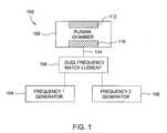
- FIG. 1depicts an exemplary block diagram of the RF structure of the present invention
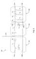
- FIG. 2is a schematic diagram of one embodiment of the matching circuit of the present invention.
- FIG. 3Ais a graph depicting the tune space shifting due to shunt variation of complimentary frequency elements
- FIG. 3Bis a graph depicting the tune space shifting due to series component variation of complimentary frequency elements
- FIG. 4is a graph of the tune space of the variable shunt matching circuit of the present invention.
- FIG. 5is an illustrative schematic diagram of a plasma enhanced processing chamber having one embodiment of a dual frequency matching circuit.
- the present inventiongenerally relates to semiconductor substrate processing in a plasma enhanced semiconductor processing chamber. More specifically, the present invention is a dual frequency, variable shunt matching circuit for coupling two RF sources through a single feed to an electrode in a plasma enhanced semiconductor processing chamber.
- FIG. 1depicts a simplified block diagram of a plasma enhanced semiconductor processing chamber having a dual frequency, variable shunt matching circuit.
- a plasma enhanced processing chamber 100includes a chamber 102 , two RF power sources 104 , 106 and a dual frequency matching circuit 108 .
- the chamber 102includes a powered electrode 110 and a grounded electrode 112 .
- a single feed line 114 from the dual frequency matching circuit 108electrically couples the sources 104 , 106 to the powered electrode 110 .
- the chamber 102is otherwise similar to a conventional plasma enhanced processing chamber.
- the RF sources 104 , 106are independent, frequency-tuned RF generators.
- the RF sources 104 , 106may be configured to provide RF power to the chamber 102 in any desired frequency to control characteristics of the plasma. Both frequencies may be selected to control the same plasma characteristic or, alternatively, to control different plasma characteristics.
- one of the RF sources 104 , 106is capable of providing high frequency power to excite the plasma and dissociate ions in the plasma and the other one of the RF sources 104 , 406 is capable of providing low frequency power to modulate the plasma sheath voltage.
- the source 104may be generally capable of generating a frequency in the range of from about 12.8 MHz to about 14.3 MHz at up to 5000 W of either continuous or pulsed power.
- the source 106may be generally capable of generating a frequency in the range of from about 1.8 MHz to about 2.2 MHz at up to 5000 W of either continuous or pulsed power. It is contemplated that other frequencies may be employed.
- the dual frequency matching circuit 108generally includes two matching sub-circuits in which the series elements are fixed and in which the shunt elements provide a variable impedance to ground.
- the matching circuit 108includes two inputs that are connected to independent frequency tuned RF power sources 104 , 106 at two separate frequencies and provides a common RF output to the processing chamber 102 .
- the matching circuit 108operates to match the impedance of the sources 104 , 106 (typically 50 ⁇ ) to that of the processing chamber 102 .
- the two match sub-circuitsare L-type circuits, however, other common match circuit configurations, such as ⁇ and T types can be employed.
- FIG. 2is a representative circuit diagram of one embodiment of a dual frequency matching circuit 108 having dual L-type match topography.
- the matching circuit 108generally includes a low frequency (first) tuning sub-circuit 202 , a high frequency (second) tuning sub-circuit 204 , and a generator isolation sub-circuit 206 .
- First sub-circuit 202comprises variable capacitor C 1 , inductor L 1 and capacitor C 2 .
- the variable capacitor C 1is shunted across the input terminals 210 A, 210 B from the 2 MHz source and the inductor L 1 and capacitor C 2 are connected in series from the input terminals 210 A and 210 B to the common output terminal 212 .
- variable capacitor C 1is nominally variable from about 300 pF to about 1500 pF
- inductor L 1is about 30 ⁇ H
- capacitor C 2is about 300 pF.
- the generator isolation sub-circuit 206comprises a ladder topology having three inductors L 3 , L 4 and L 5 and three capacitors C 5 , C 6 and C 7 .
- This sub-circuitis tuned to block the 2 MHz signal from being coupled to the 13 MHz source.
- Inductor L 5is coupled across input terminals 214 A, 214 B.
- the capacitors C 7 , C 6 and C 5are coupled in series from the input terminal 214 A to an input 216 A to the 13 MHz tuning circuit 204 .
- the inductors L 4 and L 3are respectively coupled in parallel from the junction of capacitors C 7 and C 6 and capacitors C 6 and C 5 .
- the inductors L 4 and L 5are about 2 ⁇ H and inductor L 3 is about 1 ⁇ H.
- the capacitors C 6 and C 7are about 400 pF and capacitor L 5 is about 800 pF.
- Second sub-circuit 204comprises capacitor C 3 , inductor L 2 and variable capacitor C 4 .
- the variable capacitor C 4is shunted across input terminals 216 A, 216 B from the generator isolation sub-circuit 206 and the inductor L 2 and capacitor C 3 are connected in series from the input terminals 216 A and 216 B to the common output terminal 212 .
- variable capacitor C 4is nominally variable from about 400 pF to about 1200 pF
- inductor L 2is about 2.4 ⁇ H
- capacitor C 3is about 67 pF.
- the series and shunt elementsare varied, or the elements are fixed and the source frequency is varied to achieve an impedance match between a source and the load (e.g., the plasma).
- the elements responsible for matching one of the source frequenciescan impact the load impedance seen by the elements responsible for matching the other source frequency.
- FIGS. 3A and 3Bshow how the tune space for 2 MHz and 13 MHz shifts when the other frequency's match elements are varied.
- the shunt componentse.g., capacitors C 1 and C 4 in FIG.
- FIG. 3Bdepicts the effect of varying the series component at 13 MHz.
- the 2 MHz tune spaceshifts. This is shown by the shift in lines 306 and 308 , which no longer overlap.
- FIG. 4depicts a plot of the tune space seen using the matching circuit 108 of FIG. 2 .
- This configurationcan be contained in either a fixed match condition, where the component values are set prior to a process run and the values are fixed for the entire run, or the circuit 108 can be implemented in a frequency/shunt autotune match configuration, where the frequency of the generator is tuned to establish the azimuthal tuning direction of the matching circuit and the variable shunts (capacitors C 2 and C 4 ) will set the radial tuning direction.
- These two tuning mechanisms(frequency tuning and shunt tuning) operate in perpendicular directions in the tune space and can independently tune to the optimal condition given the appropriate time response for an autotuning algorithm. As such, this form of tuning prevents unstable feedback between the two systems that may cause an un-tunable condition.
- Examples of plasma enhanced semiconductor processing chambersthat may be adapted to benefit from the present invention include, but are not limited to, the eMaxTM, MXP®, and ENABLERTM processing chambers, all available from Applied Materials, Inc. of Santa Clara, Calif.
- the eMaxTM processing chamberis described in U.S. Pat. No. 6,113,731, issued Sep. 5, 2000 to Shan et al.
- the MXP® processing chamberis described in U.S. Pat. No. 5,534,108, issued Jul. 9, 1669 to Qian et al., and U.S. Pat. No. 5,674,321, issued Oct. 7, 1997 to Pu et al.
- the ENABLERTM processing chamberis described in U.S. Pat. No. 6,528,751, issued Mar. 4, 2003 to Hoffman et al. Each of these above-mentioned patents are hereby incorporated by reference in their entireties.
- FIG. 5depicts a partial schematic, cross-section view of a capacitively coupled, plasma enhanced processing chamber 500 suitable for use with the present invention.
- a process chamber 500includes a grounded chamber body 502 and at least one coil segment 518 disposed proximate to the exterior of the chamber body 502 .
- the process chamber 500also includes a wafer support pedestal 516 disposed within the chamber body 502 and spaced apart from a gas inlet 532 .
- the wafer support pedestal 516comprises a cathode 527 and an electrostatic chuck 526 for retaining a substrate 514 beneath the gas inlet 532 .
- the electrostatic chuck 526is driven by a DC power supply 520 to develop an electrostatic force that holds the substrate on the chuck surface.
- the cathode 527is coupled to a pair of RF bias sources 104 , 106 through a dual frequency, variable shunt matching circuit 108 .
- the bias sources 104 , 106are generally capable of producing an RF signal having a frequency of from about 50 kHz to about 14.2 MHz and a power of between about 0 and about 5000 Watts.
- the dual frequency, variable shunt matching circuit 108matches the impedance of the sources 104 , 106 to the plasma impedance.
- a single feed 114couples energy from both sources to the support pedestal 516 .
- the gas inlet 532may comprise one or more nozzles or a showerhead.
- the gas inlet 532may comprise a plurality of gas distribution zones such that various gases—which, when ignited, form a plasma 510 —can be supplied to the chamber body 502 using a specific gas distribution gradient.
- the gas inlet 532may form an upper electrode 528 that opposes the support pedestal 516 .
- a substrate 514is disposed in the processing chamber 500 and held to the support pedestal 516 by the electrostatic chuck 526 .
- a process gasis introduced into the chamber body 502 through the gas inlet 532 by the gas source 508 .
- a vacuum pumpnot shown, maintains the pressure inside the chamber body 502 at operating pressures—typically between about 10 mTorr to about 20 Torr.
- the RF source 104provides about 5000 W of RF voltage at 13.56 MHz to the cathode 527 through the dual frequency, variable shunt matching circuit 108 , thereby exciting the gas inside the chamber body 502 and forming a plasma 510 .
- the RF source 106provides about 5000 W of RF voltage at a frequency of about 2 MHz to the cathode 527 through the dual frequency, variable shunt matching circuit 108 .
- the RF source 106provides bias power that both self-biases the substrate and modulates the plasma sheath. After a period of time, or the detection of a specific endpoint, the plasma is extinguished.
Landscapes
- Physics & Mathematics (AREA)
- Engineering & Computer Science (AREA)
- Plasma & Fusion (AREA)
- Chemical & Material Sciences (AREA)
- Analytical Chemistry (AREA)
- Spectroscopy & Molecular Physics (AREA)
- Plasma Technology (AREA)
- Drying Of Semiconductors (AREA)
- Chemical Vapour Deposition (AREA)
Abstract
Description
- This application claims the benefit of U.S. Provisional Application No. 60/530,807 filed Dec. 18, 2003, which is hereby incorporated by reference in its entirety.
- 1. Field of the Invention
- The present invention generally relates to semiconductor substrate processing systems and, more particularly, to matching circuits for matching the impedance of a plurality of RF sources coupled to a single electrode to the impedance of a plasma.
- 2. Description of the Related Art
- Plasma enhanced semiconductor processing chambers are widely used in the manufacture of integrated devices. In most plasma enhanced semiconductor chambers, multiple radio frequency (RF) generators are utilized to form and control the plasma. Some plasma enhanced processing chambers feed RF power from multiple sources to a single electrode that couples the power to the plasma. However, in those embodiments, each RF source generally requires separate feed structures (e.g., separate RF generator, match output, coaxial cables to the electrode, and the like).
- Therefore, there is a need for an improved apparatus for semiconductor substrate processing that utilizes a single feed structure to couple RF power from multiple RF sources to an electrode.
- So that the manner in which the above recited features, advantages and objects of the present invention are attained and can be understood in detail, a more particular description of the invention, briefly summarized above, may be had by reference to the embodiments thereof which are illustrated in the appended drawings. It is to be noted, however, that the appended drawings illustrate only typical embodiments of this invention and are therefore not to be considered limiting of its scope, for the invention may admit to other equally effective embodiments.
FIG. 1 depicts an exemplary block diagram of the RF structure of the present invention;FIG. 2 is a schematic diagram of one embodiment of the matching circuit of the present invention;FIG. 3A is a graph depicting the tune space shifting due to shunt variation of complimentary frequency elements;FIG. 3B is a graph depicting the tune space shifting due to series component variation of complimentary frequency elements;FIG. 4 is a graph of the tune space of the variable shunt matching circuit of the present invention; andFIG. 5 is an illustrative schematic diagram of a plasma enhanced processing chamber having one embodiment of a dual frequency matching circuit.- To facilitate understanding, identical reference numerals have been used, where possible, to designate identical elements that are common to the figures.
- The present invention generally relates to semiconductor substrate processing in a plasma enhanced semiconductor processing chamber. More specifically, the present invention is a dual frequency, variable shunt matching circuit for coupling two RF sources through a single feed to an electrode in a plasma enhanced semiconductor processing chamber.
FIG. 1 depicts a simplified block diagram of a plasma enhanced semiconductor processing chamber having a dual frequency, variable shunt matching circuit. A plasma enhancedprocessing chamber 100 according to the present invention includes achamber 102, twoRF power sources frequency matching circuit 108. Thechamber 102 includes a poweredelectrode 110 and a groundedelectrode 112. Asingle feed line 114 from the dualfrequency matching circuit 108 electrically couples thesources electrode 110. Thechamber 102 is otherwise similar to a conventional plasma enhanced processing chamber.- The
RF sources RF sources chamber 102 in any desired frequency to control characteristics of the plasma. Both frequencies may be selected to control the same plasma characteristic or, alternatively, to control different plasma characteristics. For example, in one embodiment, one of theRF sources RF sources 104,406 is capable of providing low frequency power to modulate the plasma sheath voltage. For example, in one embodiment, thesource 104 may be generally capable of generating a frequency in the range of from about 12.8 MHz to about 14.3 MHz at up to 5000 W of either continuous or pulsed power. Thesource 106 may be generally capable of generating a frequency in the range of from about 1.8 MHz to about 2.2 MHz at up to 5000 W of either continuous or pulsed power. It is contemplated that other frequencies may be employed. - The dual
frequency matching circuit 108 generally includes two matching sub-circuits in which the series elements are fixed and in which the shunt elements provide a variable impedance to ground. Thematching circuit 108 includes two inputs that are connected to independent frequency tunedRF power sources processing chamber 102. Thematching circuit 108 operates to match the impedance of thesources 104,106 (typically 50 Ω) to that of theprocessing chamber 102. In one embodiment, the two match sub-circuits are L-type circuits, however, other common match circuit configurations, such as π and T types can be employed. FIG. 2 is a representative circuit diagram of one embodiment of a dualfrequency matching circuit 108 having dual L-type match topography. The matchingcircuit 108 generally includes a low frequency (first)tuning sub-circuit 202, a high frequency (second)tuning sub-circuit 204, and agenerator isolation sub-circuit 206.First sub-circuit 202 comprises variable capacitor C1, inductor L1and capacitor C2. The variable capacitor C1is shunted across theinput terminals input terminals common output terminal 212. In one embodiment, variable capacitor C1is nominally variable from about 300 pF to about 1500 pF, inductor L1is about 30 μH, and capacitor C2is about 300 pF.- The
generator isolation sub-circuit 206 comprises a ladder topology having three inductors L3, L4and L5and three capacitors C5, C6and C7. This sub-circuit is tuned to block the 2 MHz signal from being coupled to the 13 MHz source. Inductor L5is coupled acrossinput terminals input terminal 214A to aninput 216A to the 13MHz tuning circuit 204. The inductors L4and L3are respectively coupled in parallel from the junction of capacitors C7and C6and capacitors C6and C5. In one embodiment, the inductors L4and L5are about 2 μH and inductor L3is about 1 μH. The capacitors C6and C7are about 400 pF and capacitor L5is about 800 pF. Second sub-circuit 204 comprises capacitor C3, inductor L2and variable capacitor C4. The variable capacitor C4is shunted acrossinput terminals generator isolation sub-circuit 206 and the inductor L2and capacitor C3are connected in series from theinput terminals common output terminal 212. In one embodiment, variable capacitor C4is nominally variable from about 400 pF to about 1200 pF, inductor L2is about 2.4 μH, and capacitor C3is about 67 pF.- Typically, in the current state of the art technology for impedance matching, either the series and shunt elements are varied, or the elements are fixed and the source frequency is varied to achieve an impedance match between a source and the load (e.g., the plasma). Where the series and shunt elements are varied, the elements responsible for matching one of the source frequencies can impact the load impedance seen by the elements responsible for matching the other source frequency. For example,
FIGS. 3A and 3B show how the tune space for 2 MHz and 13 MHz shifts when the other frequency's match elements are varied. InFIG. 3A , the shunt components (e.g., capacitors C1and C4inFIG. 2 ) are shown to have little or no effect on the other frequency's tune space (as depicted by overlayinglines FIG. 2 ) is varied, the tune space for the other frequency shifts.FIG. 3B depicts the effect of varying the series component at 13 MHz. When the 13 MHz series component is varied, the 2 MHz tune space shifts. This is shown by the shift inlines - The design of the present invention, however, as discussed above with reference to
FIGS. 1 and 2 , results in a match tune space that can be varied by shunt component tuning without the undesirable side-effect on the other frequency's tune space. Consequently, the complimentary frequency tune space remains unaffected, and a zero reflected power tune space can be realized over a large impedance range. - For example,
FIG. 4 depicts a plot of the tune space seen using thematching circuit 108 ofFIG. 2 . This configuration can be contained in either a fixed match condition, where the component values are set prior to a process run and the values are fixed for the entire run, or thecircuit 108 can be implemented in a frequency/shunt autotune match configuration, where the frequency of the generator is tuned to establish the azimuthal tuning direction of the matching circuit and the variable shunts (capacitors C2and C4) will set the radial tuning direction. These two tuning mechanisms (frequency tuning and shunt tuning) operate in perpendicular directions in the tune space and can independently tune to the optimal condition given the appropriate time response for an autotuning algorithm. As such, this form of tuning prevents unstable feedback between the two systems that may cause an un-tunable condition. - Examples of plasma enhanced semiconductor processing chambers that may be adapted to benefit from the present invention include, but are not limited to, the eMax™, MXP®, and ENABLER™ processing chambers, all available from Applied Materials, Inc. of Santa Clara, Calif. The eMax™ processing chamber is described in U.S. Pat. No. 6,113,731, issued Sep. 5, 2000 to Shan et al. The MXP® processing chamber is described in U.S. Pat. No. 5,534,108, issued Jul. 9, 1669 to Qian et al., and U.S. Pat. No. 5,674,321, issued Oct. 7, 1997 to Pu et al. The ENABLER™ processing chamber is described in U.S. Pat. No. 6,528,751, issued Mar. 4, 2003 to Hoffman et al. Each of these above-mentioned patents are hereby incorporated by reference in their entireties.
FIG. 5 depicts a partial schematic, cross-section view of a capacitively coupled, plasma enhancedprocessing chamber 500 suitable for use with the present invention. In one embodiment, aprocess chamber 500 includes a groundedchamber body 502 and at least onecoil segment 518 disposed proximate to the exterior of thechamber body 502. Theprocess chamber 500 also includes awafer support pedestal 516 disposed within thechamber body 502 and spaced apart from agas inlet 532. Thewafer support pedestal 516 comprises acathode 527 and an electrostatic chuck526 for retaining asubstrate 514 beneath thegas inlet 532.- The electrostatic chuck526 is driven by a
DC power supply 520 to develop an electrostatic force that holds the substrate on the chuck surface. Thecathode 527 is coupled to a pair of RF biassources shunt matching circuit 108. The bias sources104,106 are generally capable of producing an RF signal having a frequency of from about 50 kHz to about 14.2 MHz and a power of between about 0 and about 5000 Watts. The dual frequency, variableshunt matching circuit 108 matches the impedance of thesources single feed 114 couples energy from both sources to thesupport pedestal 516. - The
gas inlet 532 may comprise one or more nozzles or a showerhead. Thegas inlet 532 may comprise a plurality of gas distribution zones such that various gases—which, when ignited, form aplasma 510—can be supplied to thechamber body 502 using a specific gas distribution gradient. Thegas inlet 532 may form anupper electrode 528 that opposes thesupport pedestal 516. - In operation, a
substrate 514 is disposed in theprocessing chamber 500 and held to thesupport pedestal 516 by the electrostatic chuck526. A process gas is introduced into thechamber body 502 through thegas inlet 532 by thegas source 508. A vacuum pump, not shown, maintains the pressure inside thechamber body 502 at operating pressures—typically between about 10 mTorr to about 20 Torr. - The
RF source 104 provides about 5000 W of RF voltage at 13.56 MHz to thecathode 527 through the dual frequency, variableshunt matching circuit 108, thereby exciting the gas inside thechamber body 502 and forming aplasma 510. TheRF source 106 provides about 5000 W of RF voltage at a frequency of about 2 MHz to thecathode 527 through the dual frequency, variableshunt matching circuit 108. TheRF source 106 provides bias power that both self-biases the substrate and modulates the plasma sheath. After a period of time, or the detection of a specific endpoint, the plasma is extinguished. - While the foregoing is directed to the illustrative embodiment of the present invention, other and further embodiments of the invention may be devised without departing from the basic scope thereof, and the scope thereof is determined by the claims that follow.
Claims (16)
Priority Applications (6)
| Application Number | Priority Date | Filing Date | Title |
|---|---|---|---|
| US10/823,371US7879185B2 (en) | 2003-12-18 | 2004-04-12 | Dual frequency RF match |
| KR1020087022027AKR101027090B1 (en) | 2003-12-18 | 2004-11-19 | Impedance matching apparatus |
| JP2006545671AJP2007515761A (en) | 2003-12-18 | 2004-11-19 | Dual frequency RF matching |
| PCT/US2004/039081WO2005066997A2 (en) | 2003-12-18 | 2004-11-19 | Dual frequency rf match |
| CN2009101592975ACN101630624B (en) | 2003-12-18 | 2004-11-19 | Dual frequency RF match |
| TW093137328ATWI355015B (en) | 2003-12-18 | 2004-12-03 | Dual frequency rf match |
Applications Claiming Priority (2)
| Application Number | Priority Date | Filing Date | Title |
|---|---|---|---|
| US53080703P | 2003-12-18 | 2003-12-18 | |
| US10/823,371US7879185B2 (en) | 2003-12-18 | 2004-04-12 | Dual frequency RF match |
Publications (2)
| Publication Number | Publication Date |
|---|---|
| US20050133163A1true US20050133163A1 (en) | 2005-06-23 |
| US7879185B2 US7879185B2 (en) | 2011-02-01 |
Family
ID=34681594
Family Applications (1)
| Application Number | Title | Priority Date | Filing Date |
|---|---|---|---|
| US10/823,371Expired - Fee RelatedUS7879185B2 (en) | 2003-12-18 | 2004-04-12 | Dual frequency RF match |
Country Status (5)
| Country | Link |
|---|---|
| US (1) | US7879185B2 (en) |
| JP (1) | JP2007515761A (en) |
| KR (1) | KR101027090B1 (en) |
| TW (1) | TWI355015B (en) |
| WO (1) | WO2005066997A2 (en) |
Cited By (47)
| Publication number | Priority date | Publication date | Assignee | Title |
|---|---|---|---|---|
| US20070026321A1 (en)* | 2005-07-29 | 2007-02-01 | Applied Materials, Inc. | Cluster tool and method for process integration in manufacturing of a photomask |
| US20070030091A1 (en)* | 2005-08-05 | 2007-02-08 | Advanced Micro-Fabrication Equipment, Inc. Asia | RF matching network of a vacuum processing chamber and corresponding configuration methods |
| US20070031609A1 (en)* | 2005-07-29 | 2007-02-08 | Ajay Kumar | Chemical vapor deposition chamber with dual frequency bias and method for manufacturing a photomask using the same |
| US20070028840A1 (en)* | 2005-08-05 | 2007-02-08 | Qing Qian | Plasma processing apparatus |
| US20080011424A1 (en)* | 2005-08-05 | 2008-01-17 | Advanced Micro-Fabrication Equipment, Inc. Asia | Multi-station decoupled reactive ion etch chamber |
| US20080102645A1 (en)* | 2006-10-31 | 2008-05-01 | Applied Materials, Inc. | Plasma for resist removal and facet control of underlying features |
| US20080131789A1 (en)* | 2005-09-28 | 2008-06-05 | Ajay Kumar | Method for photomask fabrication utilizing a carbon hard mask |
| US20090004873A1 (en)* | 2007-06-26 | 2009-01-01 | Intevac, Inc. | Hybrid etch chamber with decoupled plasma controls |
| US20090315596A1 (en)* | 2008-06-19 | 2009-12-24 | Lam Research Corporation | Matching circuit for a complex radio frequency (rf) waveform |
| US20100013572A1 (en)* | 2008-07-21 | 2010-01-21 | Applied Materials, Inc. | Apparatus for multiple frequency power application |
| US20100294433A1 (en)* | 2008-01-04 | 2010-11-25 | Nan Jianhui | Plasma processing apparatus |
| US20120000888A1 (en)* | 2010-06-30 | 2012-01-05 | Applied Materials, Inc. | Methods and apparatus for radio frequency (rf) plasma processing |
| CN102742366A (en)* | 2010-02-23 | 2012-10-17 | 株式会社普来马特 | Impedance matching apparatus |
| US20130214828A1 (en)* | 2012-02-22 | 2013-08-22 | Valcore John C, JR. | Methods and apparatus for synchronizing rf pulses in a plasma processing system |
| US8674255B1 (en)* | 2005-12-08 | 2014-03-18 | Lam Research Corporation | Apparatus and method for controlling etch uniformity |
| US20140173158A1 (en)* | 2012-12-14 | 2014-06-19 | John C. Valcore, JR. | Rate of Transfer of Data Within A Plasma System |
| CN104754851A (en)* | 2013-12-31 | 2015-07-01 | 北京北方微电子基地设备工艺研究中心有限责任公司 | Multi-frequency matcher and plasma device |
| US9082594B2 (en) | 2013-07-26 | 2015-07-14 | Lam Research Corporation | Etch rate modeling and use thereof for in-chamber and chamber-to-chamber matching |
| US9107284B2 (en) | 2013-03-13 | 2015-08-11 | Lam Research Corporation | Chamber matching using voltage control mode |
| US9114666B2 (en) | 2012-02-22 | 2015-08-25 | Lam Research Corporation | Methods and apparatus for controlling plasma in a plasma processing system |
| US9119283B2 (en) | 2013-03-14 | 2015-08-25 | Lam Research Corporation | Chamber matching for power control mode |
| US9155182B2 (en) | 2013-01-11 | 2015-10-06 | Lam Research Corporation | Tuning a parameter associated with plasma impedance |
| US20150301100A1 (en)* | 2014-04-21 | 2015-10-22 | Lam Research Corporation | Using modeling for identifying a location of a fault in an rf transmission system for a plasma system |
| US9171699B2 (en) | 2012-02-22 | 2015-10-27 | Lam Research Corporation | Impedance-based adjustment of power and frequency |
| US9197196B2 (en) | 2012-02-22 | 2015-11-24 | Lam Research Corporation | State-based adjustment of power and frequency |
| US9295148B2 (en) | 2012-12-14 | 2016-03-22 | Lam Research Corporation | Computation of statistics for statistical data decimation |
| US9320126B2 (en) | 2012-12-17 | 2016-04-19 | Lam Research Corporation | Determining a value of a variable on an RF transmission model |
| US9390893B2 (en) | 2012-02-22 | 2016-07-12 | Lam Research Corporation | Sub-pulsing during a state |
| US9408288B2 (en) | 2012-09-14 | 2016-08-02 | Lam Research Corporation | Edge ramping |
| US9455126B2 (en) | 2009-11-19 | 2016-09-27 | Lam Research Corporation | Arrangement for plasma processing system control based on RF voltage |
| US9462672B2 (en) | 2012-02-22 | 2016-10-04 | Lam Research Corporation | Adjustment of power and frequency based on three or more states |
| US9502216B2 (en) | 2013-01-31 | 2016-11-22 | Lam Research Corporation | Using modeling to determine wafer bias associated with a plasma system |
| US9530620B2 (en) | 2013-03-15 | 2016-12-27 | Lam Research Corporation | Dual control modes |
| US9536749B2 (en) | 2014-12-15 | 2017-01-03 | Lam Research Corporation | Ion energy control by RF pulse shape |
| US9594105B2 (en) | 2014-01-10 | 2017-03-14 | Lam Research Corporation | Cable power loss determination for virtual metrology |
| US9620337B2 (en) | 2013-01-31 | 2017-04-11 | Lam Research Corporation | Determining a malfunctioning device in a plasma system |
| US9779196B2 (en) | 2013-01-31 | 2017-10-03 | Lam Research Corporation | Segmenting a model within a plasma system |
| US9842725B2 (en) | 2013-01-31 | 2017-12-12 | Lam Research Corporation | Using modeling to determine ion energy associated with a plasma system |
| US20180053631A1 (en)* | 2015-10-29 | 2018-02-22 | Applied Materials, Inc. | Low Electron Temperature Etch Chamber with Independent Control Over Plasma Density, Radical Composition Ion Energy for Atomic Precision Etching |
| WO2018187292A1 (en)* | 2017-04-07 | 2018-10-11 | Lam Research Corporation | Auxiliary circuit in rf matching network for frequency tuning assisted dual-level pulsing |
| US10128090B2 (en) | 2012-02-22 | 2018-11-13 | Lam Research Corporation | RF impedance model based fault detection |
| US10157729B2 (en) | 2012-02-22 | 2018-12-18 | Lam Research Corporation | Soft pulsing |
| US10325759B2 (en) | 2012-02-22 | 2019-06-18 | Lam Research Corporation | Multiple control modes |
| US20210398774A1 (en)* | 2018-10-24 | 2021-12-23 | Jiangsu Leuven Instruments Co. Ltd | Etching device and method of inductively coupled plasma |
| US20220344130A1 (en)* | 2021-04-22 | 2022-10-27 | Mattson Technology, Inc. | Dual Frequency Matching Circuit for Inductively Coupled Plasma (ICP) Loads |
| US20230129976A1 (en)* | 2021-10-21 | 2023-04-27 | Tokyo Electron Limited | Ignition controlling method, film forming method, and film forming apparatus |
| US20230238924A1 (en)* | 2022-01-25 | 2023-07-27 | Furuno Electric Co., Ltd. | Amplifier circuit and sonar |
Families Citing this family (7)
| Publication number | Priority date | Publication date | Assignee | Title |
|---|---|---|---|---|
| CN102480831A (en)* | 2010-11-26 | 2012-05-30 | 北京北方微电子基地设备工艺研究中心有限责任公司 | Bottom electrode device and semiconductor device |
| US10553465B2 (en)* | 2016-07-25 | 2020-02-04 | Lam Research Corporation | Control of water bow in multiple stations |
| FR3058602B1 (en)* | 2016-11-08 | 2021-02-12 | Centre Nat Rech Scient | IMPEDANCE ADAPTATION CIRCUIT BETWEEN A GENERATOR AND A LOAD AT MULTIPLE FREQUENCIES, ASSEMBLY INCLUDING SUCH A CIRCUIT AND LINKED USE. |
| US10395896B2 (en) | 2017-03-03 | 2019-08-27 | Applied Materials, Inc. | Method and apparatus for ion energy distribution manipulation for plasma processing chambers that allows ion energy boosting through amplitude modulation |
| CN110870040B (en) | 2017-07-13 | 2022-05-03 | 应用材料公司 | Substrate processing method and apparatus |
| KR102024185B1 (en)* | 2018-01-11 | 2019-09-23 | (주)이큐글로벌 | Source matcher |
| KR20250021906A (en)* | 2023-08-07 | 2025-02-14 | 엠케이에스코리아 유한회사 | A Power Delivery Apparatus Transferring a Load with Combining a RF Power and a DC pulse Voltage |
Citations (17)
| Publication number | Priority date | Publication date | Assignee | Title |
|---|---|---|---|---|
| US4579618A (en)* | 1984-01-06 | 1986-04-01 | Tegal Corporation | Plasma reactor apparatus |
| US4585516A (en)* | 1985-03-04 | 1986-04-29 | Tegal Corporation | Variable duty cycle, multiple frequency, plasma reactor |
| US5273610A (en)* | 1992-06-23 | 1993-12-28 | Association Institutions For Material Sciences, Inc. | Apparatus and method for determining power in plasma processing |
| US5383019A (en)* | 1990-03-23 | 1995-01-17 | Fisons Plc | Inductively coupled plasma spectrometers and radio-frequency power supply therefor |
| US5472564A (en)* | 1988-02-09 | 1995-12-05 | Fujitsu Limited | Method of dry etching with hydrogen bromide or bromide |
| US5512130A (en)* | 1994-03-09 | 1996-04-30 | Texas Instruments Incorporated | Method and apparatus of etching a clean trench in a semiconductor material |
| US5556501A (en)* | 1989-10-03 | 1996-09-17 | Applied Materials, Inc. | Silicon scavenger in an inductively coupled RF plasma reactor |
| US5689215A (en)* | 1996-05-23 | 1997-11-18 | Lam Research Corporation | Method of and apparatus for controlling reactive impedances of a matching network connected between an RF source and an RF plasma processor |
| US5889252A (en)* | 1996-12-19 | 1999-03-30 | Lam Research Corporation | Method of and apparatus for independently controlling electric parameters of an impedance matching network |
| US6089181A (en)* | 1996-07-23 | 2000-07-18 | Tokyo Electron Limited | Plasma processing apparatus |
| US6252354B1 (en)* | 1996-11-04 | 2001-06-26 | Applied Materials, Inc. | RF tuning method for an RF plasma reactor using frequency servoing and power, voltage, current or DI/DT control |
| US6259334B1 (en)* | 1998-12-22 | 2001-07-10 | Lam Research Corporation | Methods for controlling an RF matching network |
| US6354240B1 (en)* | 1996-07-03 | 2002-03-12 | Tegal Corporation | Plasma etch reactor having a plurality of magnets |
| US20020041160A1 (en)* | 2000-04-06 | 2002-04-11 | Applied Materials, Inc. | Method for controlling etch uniformity |
| US20020046989A1 (en)* | 1998-07-13 | 2002-04-25 | Applied Komatsu Technology, Inc. | RF matching network with distributed outputs |
| US20030054647A1 (en)* | 1998-09-16 | 2003-03-20 | Tomoki Suemasa | Plasma processing method |
| US6887339B1 (en)* | 2000-09-20 | 2005-05-03 | Applied Science And Technology, Inc. | RF power supply with integrated matching network |
Family Cites Families (14)
| Publication number | Priority date | Publication date | Assignee | Title |
|---|---|---|---|---|
| US457961A (en)* | 1891-08-18 | Island | ||
| JPS57113599A (en)* | 1981-01-06 | 1982-07-15 | Kokusai Electric Co Ltd | Automatic matching device for plasma generator |
| DE3480573D1 (en)* | 1984-01-06 | 1989-12-28 | Tegal Corp | Single electrode, multiple frequency plasma apparatus |
| US5280154A (en) | 1992-01-30 | 1994-01-18 | International Business Machines Corporation | Radio frequency induction plasma processing system utilizing a uniform field coil |
| JP3251087B2 (en)* | 1993-02-16 | 2002-01-28 | 東京エレクトロン株式会社 | Plasma processing equipment |
| JPH0897199A (en)* | 1994-09-22 | 1996-04-12 | Toshiba Corp | Method of forming insulating film |
| US5688357A (en)* | 1995-02-15 | 1997-11-18 | Applied Materials, Inc. | Automatic frequency tuning of an RF power source of an inductively coupled plasma reactor |
| EP0840350A2 (en) | 1996-11-04 | 1998-05-06 | Applied Materials, Inc. | Plasma apparatus and process with filtering of plasma sheath-generated harmonics |
| JP4283360B2 (en)* | 1998-01-29 | 2009-06-24 | キヤノンアネルバ株式会社 | Plasma processing equipment |
| JP2000156370A (en)* | 1998-09-16 | 2000-06-06 | Tokyo Electron Ltd | Plasma processing method |
| JP3897582B2 (en)* | 2000-12-12 | 2007-03-28 | キヤノン株式会社 | Vacuum processing method, vacuum processing apparatus, semiconductor device manufacturing method, and semiconductor device |
| JP2003073836A (en) | 2001-08-28 | 2003-03-12 | Canon Inc | Vacuum processing method and vacuum processing apparatus |
| US6887340B2 (en) | 2001-11-13 | 2005-05-03 | Lam Research Corporation | Etch rate uniformity |
| JP3905870B2 (en)* | 2003-08-01 | 2007-04-18 | 東京エレクトロン株式会社 | Plasma processing equipment |
- 2004
- 2004-04-12USUS10/823,371patent/US7879185B2/ennot_activeExpired - Fee Related
- 2004-11-19WOPCT/US2004/039081patent/WO2005066997A2/enactiveApplication Filing
- 2004-11-19JPJP2006545671Apatent/JP2007515761A/enactivePending
- 2004-11-19KRKR1020087022027Apatent/KR101027090B1/ennot_activeExpired - Fee Related
- 2004-12-03TWTW093137328Apatent/TWI355015B/ennot_activeIP Right Cessation
Patent Citations (18)
| Publication number | Priority date | Publication date | Assignee | Title |
|---|---|---|---|---|
| US4579618A (en)* | 1984-01-06 | 1986-04-01 | Tegal Corporation | Plasma reactor apparatus |
| US4585516A (en)* | 1985-03-04 | 1986-04-29 | Tegal Corporation | Variable duty cycle, multiple frequency, plasma reactor |
| US5472564A (en)* | 1988-02-09 | 1995-12-05 | Fujitsu Limited | Method of dry etching with hydrogen bromide or bromide |
| US5556501A (en)* | 1989-10-03 | 1996-09-17 | Applied Materials, Inc. | Silicon scavenger in an inductively coupled RF plasma reactor |
| US5383019A (en)* | 1990-03-23 | 1995-01-17 | Fisons Plc | Inductively coupled plasma spectrometers and radio-frequency power supply therefor |
| US5273610A (en)* | 1992-06-23 | 1993-12-28 | Association Institutions For Material Sciences, Inc. | Apparatus and method for determining power in plasma processing |
| US5512130A (en)* | 1994-03-09 | 1996-04-30 | Texas Instruments Incorporated | Method and apparatus of etching a clean trench in a semiconductor material |
| US5689215A (en)* | 1996-05-23 | 1997-11-18 | Lam Research Corporation | Method of and apparatus for controlling reactive impedances of a matching network connected between an RF source and an RF plasma processor |
| US6354240B1 (en)* | 1996-07-03 | 2002-03-12 | Tegal Corporation | Plasma etch reactor having a plurality of magnets |
| US6089181A (en)* | 1996-07-23 | 2000-07-18 | Tokyo Electron Limited | Plasma processing apparatus |
| US6252354B1 (en)* | 1996-11-04 | 2001-06-26 | Applied Materials, Inc. | RF tuning method for an RF plasma reactor using frequency servoing and power, voltage, current or DI/DT control |
| US5889252A (en)* | 1996-12-19 | 1999-03-30 | Lam Research Corporation | Method of and apparatus for independently controlling electric parameters of an impedance matching network |
| US20020046989A1 (en)* | 1998-07-13 | 2002-04-25 | Applied Komatsu Technology, Inc. | RF matching network with distributed outputs |
| US20030054647A1 (en)* | 1998-09-16 | 2003-03-20 | Tomoki Suemasa | Plasma processing method |
| US6642149B2 (en)* | 1998-09-16 | 2003-11-04 | Tokyo Electron Limited | Plasma processing method |
| US6259334B1 (en)* | 1998-12-22 | 2001-07-10 | Lam Research Corporation | Methods for controlling an RF matching network |
| US20020041160A1 (en)* | 2000-04-06 | 2002-04-11 | Applied Materials, Inc. | Method for controlling etch uniformity |
| US6887339B1 (en)* | 2000-09-20 | 2005-05-03 | Applied Science And Technology, Inc. | RF power supply with integrated matching network |
Cited By (79)
| Publication number | Priority date | Publication date | Assignee | Title |
|---|---|---|---|---|
| US7829471B2 (en) | 2005-07-29 | 2010-11-09 | Applied Materials, Inc. | Cluster tool and method for process integration in manufacturing of a photomask |
| US20070023390A1 (en)* | 2005-07-29 | 2007-02-01 | Ajay Kumar | Cluster tool and method for process integration in manufacturing of a photomask |
| US7838433B2 (en) | 2005-07-29 | 2010-11-23 | Applied Materials, Inc. | Cluster tool and method for process integration in manufacturing of a photomask |
| US20070031609A1 (en)* | 2005-07-29 | 2007-02-08 | Ajay Kumar | Chemical vapor deposition chamber with dual frequency bias and method for manufacturing a photomask using the same |
| US7658969B2 (en) | 2005-07-29 | 2010-02-09 | Applied Materials, Inc. | Chemical vapor deposition chamber with dual frequency bias and method for manufacturing a photomask using the same |
| US20070119373A1 (en)* | 2005-07-29 | 2007-05-31 | Ajay Kumar | Chemical vapor deposition chamber with dual frequency bias and method for manufacturing a photomask using the same |
| US20070026321A1 (en)* | 2005-07-29 | 2007-02-01 | Applied Materials, Inc. | Cluster tool and method for process integration in manufacturing of a photomask |
| US8366829B2 (en) | 2005-08-05 | 2013-02-05 | Advanced Micro-Fabrication Equipment, Inc. Asia | Multi-station decoupled reactive ion etch chamber |
| US8334657B2 (en) | 2005-08-05 | 2012-12-18 | Applied Materials, Inc. | RF matching network of a vacuum processing chamber and corresponding configuration methods |
| US8414702B2 (en) | 2005-08-05 | 2013-04-09 | Advanced Micro-Fabrication Equipment, Inc. Asia | Plasma processing apparatus |
| US20080011424A1 (en)* | 2005-08-05 | 2008-01-17 | Advanced Micro-Fabrication Equipment, Inc. Asia | Multi-station decoupled reactive ion etch chamber |
| US20070028840A1 (en)* | 2005-08-05 | 2007-02-08 | Qing Qian | Plasma processing apparatus |
| US20110180000A1 (en)* | 2005-08-05 | 2011-07-28 | Qing Qian | Plasma processing apparatus |
| US7935186B2 (en) | 2005-08-05 | 2011-05-03 | Advanced Micro-Fabrication Equipment, Inc. Asia | Plasma processing apparatus |
| US7868556B2 (en)* | 2005-08-05 | 2011-01-11 | Advanced Micro-Fabrication Equipment, Inc. Asia | RF matching network of a vacuum processing chamber and corresponding configuration methods |
| US20070030091A1 (en)* | 2005-08-05 | 2007-02-08 | Advanced Micro-Fabrication Equipment, Inc. Asia | RF matching network of a vacuum processing chamber and corresponding configuration methods |
| US20080131789A1 (en)* | 2005-09-28 | 2008-06-05 | Ajay Kumar | Method for photomask fabrication utilizing a carbon hard mask |
| US20080280212A9 (en)* | 2005-09-28 | 2008-11-13 | Ajay Kumar | Method for photomask fabrication utilizing a carbon hard mask |
| US7718539B2 (en) | 2005-09-28 | 2010-05-18 | Applied Materials, Inc. | Method for photomask fabrication utilizing a carbon hard mask |
| US8674255B1 (en)* | 2005-12-08 | 2014-03-18 | Lam Research Corporation | Apparatus and method for controlling etch uniformity |
| US20080102645A1 (en)* | 2006-10-31 | 2008-05-01 | Applied Materials, Inc. | Plasma for resist removal and facet control of underlying features |
| US7758763B2 (en) | 2006-10-31 | 2010-07-20 | Applied Materials, Inc. | Plasma for resist removal and facet control of underlying features |
| EP2012342A3 (en)* | 2007-06-26 | 2010-09-01 | Intevac, Inc. | Hybrid etch chamber with decoupled plasma controls |
| US20090004873A1 (en)* | 2007-06-26 | 2009-01-01 | Intevac, Inc. | Hybrid etch chamber with decoupled plasma controls |
| US20100294433A1 (en)* | 2008-01-04 | 2010-11-25 | Nan Jianhui | Plasma processing apparatus |
| US7811410B2 (en) | 2008-06-19 | 2010-10-12 | Lam Research Corporation | Matching circuit for a complex radio frequency (RF) waveform |
| WO2009155352A3 (en)* | 2008-06-19 | 2010-03-25 | Lam Research Corporation | Matching circuit for a complex radio frequency (rf) waveform |
| US20090315596A1 (en)* | 2008-06-19 | 2009-12-24 | Lam Research Corporation | Matching circuit for a complex radio frequency (rf) waveform |
| US20100013572A1 (en)* | 2008-07-21 | 2010-01-21 | Applied Materials, Inc. | Apparatus for multiple frequency power application |
| US7994872B2 (en) | 2008-07-21 | 2011-08-09 | Applied Materials, Inc. | Apparatus for multiple frequency power application |
| US8237517B2 (en) | 2008-07-21 | 2012-08-07 | Applied Materials, Inc. | Apparatus for multiple frequency power application |
| WO2010011643A3 (en)* | 2008-07-21 | 2010-05-14 | Applied Materials, Inc. | Apparatus for multiple frequency power application |
| US9455126B2 (en) | 2009-11-19 | 2016-09-27 | Lam Research Corporation | Arrangement for plasma processing system control based on RF voltage |
| US8884520B2 (en)* | 2010-02-23 | 2014-11-11 | Plasmart Inc. | Impedance matching apparatus |
| US20120306367A1 (en)* | 2010-02-23 | 2012-12-06 | Jae Hyun Kim | Impedance matching apparatus |
| CN102742366A (en)* | 2010-02-23 | 2012-10-17 | 株式会社普来马特 | Impedance matching apparatus |
| US20120000888A1 (en)* | 2010-06-30 | 2012-01-05 | Applied Materials, Inc. | Methods and apparatus for radio frequency (rf) plasma processing |
| US10325759B2 (en) | 2012-02-22 | 2019-06-18 | Lam Research Corporation | Multiple control modes |
| US9368329B2 (en)* | 2012-02-22 | 2016-06-14 | Lam Research Corporation | Methods and apparatus for synchronizing RF pulses in a plasma processing system |
| US10157729B2 (en) | 2012-02-22 | 2018-12-18 | Lam Research Corporation | Soft pulsing |
| US10128090B2 (en) | 2012-02-22 | 2018-11-13 | Lam Research Corporation | RF impedance model based fault detection |
| US9462672B2 (en) | 2012-02-22 | 2016-10-04 | Lam Research Corporation | Adjustment of power and frequency based on three or more states |
| US9114666B2 (en) | 2012-02-22 | 2015-08-25 | Lam Research Corporation | Methods and apparatus for controlling plasma in a plasma processing system |
| US20130214828A1 (en)* | 2012-02-22 | 2013-08-22 | Valcore John C, JR. | Methods and apparatus for synchronizing rf pulses in a plasma processing system |
| US9390893B2 (en) | 2012-02-22 | 2016-07-12 | Lam Research Corporation | Sub-pulsing during a state |
| US9171699B2 (en) | 2012-02-22 | 2015-10-27 | Lam Research Corporation | Impedance-based adjustment of power and frequency |
| US9197196B2 (en) | 2012-02-22 | 2015-11-24 | Lam Research Corporation | State-based adjustment of power and frequency |
| US9408288B2 (en) | 2012-09-14 | 2016-08-02 | Lam Research Corporation | Edge ramping |
| US9043525B2 (en)* | 2012-12-14 | 2015-05-26 | Lam Research Corporation | Optimizing a rate of transfer of data between an RF generator and a host system within a plasma tool |
| US20140173158A1 (en)* | 2012-12-14 | 2014-06-19 | John C. Valcore, JR. | Rate of Transfer of Data Within A Plasma System |
| US9295148B2 (en) | 2012-12-14 | 2016-03-22 | Lam Research Corporation | Computation of statistics for statistical data decimation |
| US9320126B2 (en) | 2012-12-17 | 2016-04-19 | Lam Research Corporation | Determining a value of a variable on an RF transmission model |
| US9155182B2 (en) | 2013-01-11 | 2015-10-06 | Lam Research Corporation | Tuning a parameter associated with plasma impedance |
| US9502216B2 (en) | 2013-01-31 | 2016-11-22 | Lam Research Corporation | Using modeling to determine wafer bias associated with a plasma system |
| US9620337B2 (en) | 2013-01-31 | 2017-04-11 | Lam Research Corporation | Determining a malfunctioning device in a plasma system |
| US9779196B2 (en) | 2013-01-31 | 2017-10-03 | Lam Research Corporation | Segmenting a model within a plasma system |
| US9842725B2 (en) | 2013-01-31 | 2017-12-12 | Lam Research Corporation | Using modeling to determine ion energy associated with a plasma system |
| US9107284B2 (en) | 2013-03-13 | 2015-08-11 | Lam Research Corporation | Chamber matching using voltage control mode |
| US9119283B2 (en) | 2013-03-14 | 2015-08-25 | Lam Research Corporation | Chamber matching for power control mode |
| US9530620B2 (en) | 2013-03-15 | 2016-12-27 | Lam Research Corporation | Dual control modes |
| US9502221B2 (en) | 2013-07-26 | 2016-11-22 | Lam Research Corporation | Etch rate modeling and use thereof with multiple parameters for in-chamber and chamber-to-chamber matching |
| US9082594B2 (en) | 2013-07-26 | 2015-07-14 | Lam Research Corporation | Etch rate modeling and use thereof for in-chamber and chamber-to-chamber matching |
| CN104754851A (en)* | 2013-12-31 | 2015-07-01 | 北京北方微电子基地设备工艺研究中心有限责任公司 | Multi-frequency matcher and plasma device |
| US9594105B2 (en) | 2014-01-10 | 2017-03-14 | Lam Research Corporation | Cable power loss determination for virtual metrology |
| US10950421B2 (en)* | 2014-04-21 | 2021-03-16 | Lam Research Corporation | Using modeling for identifying a location of a fault in an RF transmission system for a plasma system |
| US20150301100A1 (en)* | 2014-04-21 | 2015-10-22 | Lam Research Corporation | Using modeling for identifying a location of a fault in an rf transmission system for a plasma system |
| US9536749B2 (en) | 2014-12-15 | 2017-01-03 | Lam Research Corporation | Ion energy control by RF pulse shape |
| US20180053631A1 (en)* | 2015-10-29 | 2018-02-22 | Applied Materials, Inc. | Low Electron Temperature Etch Chamber with Independent Control Over Plasma Density, Radical Composition Ion Energy for Atomic Precision Etching |
| TWI840327B (en)* | 2017-04-07 | 2024-05-01 | 美商蘭姆研究公司 | Rf matching circuit control system and impedance matching method |
| CN110945622A (en)* | 2017-04-07 | 2020-03-31 | 朗姆研究公司 | Auxiliary Circuit for Frequency Tuning Auxiliary Bilevel Pulse in RF Matching Network |
| US10879044B2 (en) | 2017-04-07 | 2020-12-29 | Lam Research Corporation | Auxiliary circuit in RF matching network for frequency tuning assisted dual-level pulsing |
| WO2018187292A1 (en)* | 2017-04-07 | 2018-10-11 | Lam Research Corporation | Auxiliary circuit in rf matching network for frequency tuning assisted dual-level pulsing |
| US20210398774A1 (en)* | 2018-10-24 | 2021-12-23 | Jiangsu Leuven Instruments Co. Ltd | Etching device and method of inductively coupled plasma |
| US20220344130A1 (en)* | 2021-04-22 | 2022-10-27 | Mattson Technology, Inc. | Dual Frequency Matching Circuit for Inductively Coupled Plasma (ICP) Loads |
| US12040159B2 (en)* | 2021-04-22 | 2024-07-16 | Beijing E-town Semiconductor Technology Co., Ltd. | Dual frequency matching circuit for inductively coupled plasma (ICP) loads |
| US12400831B2 (en) | 2021-04-22 | 2025-08-26 | Beijing E-town Semiconductor Technology Co., Ltd. | Dual frequency matching circuit for inductively coupled plasma (ICP) loads |
| US20230129976A1 (en)* | 2021-10-21 | 2023-04-27 | Tokyo Electron Limited | Ignition controlling method, film forming method, and film forming apparatus |
| US20230238924A1 (en)* | 2022-01-25 | 2023-07-27 | Furuno Electric Co., Ltd. | Amplifier circuit and sonar |
| US12395131B2 (en)* | 2022-01-25 | 2025-08-19 | Furuno Electric Co., Ltd. | Amplifier circuit and sonar |
Also Published As
| Publication number | Publication date |
|---|---|
| KR20080086556A (en) | 2008-09-25 |
| US7879185B2 (en) | 2011-02-01 |
| WO2005066997A3 (en) | 2005-09-29 |
| TW200522145A (en) | 2005-07-01 |
| KR101027090B1 (en) | 2011-04-05 |
| WO2005066997A2 (en) | 2005-07-21 |
| TWI355015B (en) | 2011-12-21 |
| JP2007515761A (en) | 2007-06-14 |
Similar Documents
| Publication | Publication Date | Title |
|---|---|---|
| US7879185B2 (en) | Dual frequency RF match | |
| US7431857B2 (en) | Plasma generation and control using a dual frequency RF source | |
| US12148595B2 (en) | Plasma uniformity control in pulsed DC plasma chamber | |
| KR102038617B1 (en) | Plasma treatment method and plasma treatment device | |
| KR101029948B1 (en) | Systems and Methods for Controlling Plasma with Coupling Circuit Adjustable to Ground | |
| US7415940B2 (en) | Plasma processor | |
| US7510665B2 (en) | Plasma generation and control using dual frequency RF signals | |
| US20080251207A1 (en) | Multiple frequency plasma chamber, switchable rf system, and processes using same | |
| TW201342467A (en) | Plasma processing device | |
| US12400831B2 (en) | Dual frequency matching circuit for inductively coupled plasma (ICP) loads | |
| CN100550273C (en) | Dual Frequency RF Matching | |
| US20040182319A1 (en) | Inductively coupled plasma generation system with a parallel antenna array having evenly distributed power input and ground nodes | |
| US11328900B2 (en) | Plasma ignition circuit | |
| US20250046576A1 (en) | Plasma processing assembly for rf and pvt integration | |
| CN120693675A (en) | RF splitter components that can achieve different spatial outputs as required | |
| TWI442838B (en) | A single matching network, a construction method thereof, and a matching network radio frequency power source system | |
| KR100902435B1 (en) | Impedance matching apparatus | |
| US8445988B2 (en) | Apparatus and method for plasma processing | |
| TWI383712B (en) | An RF power source system and a plasma reaction chamber using the RF power source system | |
| TWI423737B (en) | An RF power source system and a plasma reaction chamber using the RF power source system |
Legal Events
| Date | Code | Title | Description |
|---|---|---|---|
| AS | Assignment | Owner name:APPLIED MATERIALS, INC., CALIFORNIA Free format text:ASSIGNMENT OF ASSIGNORS INTEREST;ASSIGNORS:SHANNON, STEVEN C.;HOLLAND, JOHN;REEL/FRAME:015212/0092;SIGNING DATES FROM 20040406 TO 20040409 Owner name:APPLIED MATERIALS, INC., CALIFORNIA Free format text:ASSIGNMENT OF ASSIGNORS INTEREST;ASSIGNORS:SHANNON, STEVEN C.;HOLLAND, JOHN;SIGNING DATES FROM 20040406 TO 20040409;REEL/FRAME:015212/0092 | |
| STCF | Information on status: patent grant | Free format text:PATENTED CASE | |
| FPAY | Fee payment | Year of fee payment:4 | |
| MAFP | Maintenance fee payment | Free format text:PAYMENT OF MAINTENANCE FEE, 8TH YEAR, LARGE ENTITY (ORIGINAL EVENT CODE: M1552) Year of fee payment:8 | |
| FEPP | Fee payment procedure | Free format text:MAINTENANCE FEE REMINDER MAILED (ORIGINAL EVENT CODE: REM.); ENTITY STATUS OF PATENT OWNER: LARGE ENTITY | |
| LAPS | Lapse for failure to pay maintenance fees | Free format text:PATENT EXPIRED FOR FAILURE TO PAY MAINTENANCE FEES (ORIGINAL EVENT CODE: EXP.); ENTITY STATUS OF PATENT OWNER: LARGE ENTITY | |
| STCH | Information on status: patent discontinuation | Free format text:PATENT EXPIRED DUE TO NONPAYMENT OF MAINTENANCE FEES UNDER 37 CFR 1.362 | |
| FP | Lapsed due to failure to pay maintenance fee | Effective date:20230201 |