US20050127362A1 - Sectional field effect devices and method of fabrication - Google Patents
Sectional field effect devices and method of fabricationDownload PDFInfo
- Publication number
- US20050127362A1 US20050127362A1US10/732,322US73232203AUS2005127362A1US 20050127362 A1US20050127362 A1US 20050127362A1US 73232203 AUS73232203 AUS 73232203AUS 2005127362 A1US2005127362 A1US 2005127362A1
- Authority
- US
- United States
- Prior art keywords
- layer
- field effect
- effect device
- oriented section
- selecting
- Prior art date
- Legal status (The legal status is an assumption and is not a legal conclusion. Google has not performed a legal analysis and makes no representation as to the accuracy of the status listed.)
- Granted
Links
Images


Classifications
- H—ELECTRICITY
- H01—ELECTRIC ELEMENTS
- H01L—SEMICONDUCTOR DEVICES NOT COVERED BY CLASS H10
- H01L21/00—Processes or apparatus adapted for the manufacture or treatment of semiconductor or solid state devices or of parts thereof
- H01L21/02—Manufacture or treatment of semiconductor devices or of parts thereof
- H01L21/04—Manufacture or treatment of semiconductor devices or of parts thereof the devices having potential barriers, e.g. a PN junction, depletion layer or carrier concentration layer
- H01L21/18—Manufacture or treatment of semiconductor devices or of parts thereof the devices having potential barriers, e.g. a PN junction, depletion layer or carrier concentration layer the devices having semiconductor bodies comprising elements of Group IV of the Periodic Table or AIIIBV compounds with or without impurities, e.g. doping materials
- H—ELECTRICITY
- H10—SEMICONDUCTOR DEVICES; ELECTRIC SOLID-STATE DEVICES NOT OTHERWISE PROVIDED FOR
- H10D—INORGANIC ELECTRIC SEMICONDUCTOR DEVICES
- H10D30/00—Field-effect transistors [FET]
- H10D30/01—Manufacture or treatment
- H10D30/021—Manufacture or treatment of FETs having insulated gates [IGFET]
- H10D30/024—Manufacture or treatment of FETs having insulated gates [IGFET] of fin field-effect transistors [FinFET]
- H—ELECTRICITY
- H10—SEMICONDUCTOR DEVICES; ELECTRIC SOLID-STATE DEVICES NOT OTHERWISE PROVIDED FOR
- H10D—INORGANIC ELECTRIC SEMICONDUCTOR DEVICES
- H10D30/00—Field-effect transistors [FET]
- H10D30/60—Insulated-gate field-effect transistors [IGFET]
- H10D30/62—Fin field-effect transistors [FinFET]
- H—ELECTRICITY
- H10—SEMICONDUCTOR DEVICES; ELECTRIC SOLID-STATE DEVICES NOT OTHERWISE PROVIDED FOR
- H10D—INORGANIC ELECTRIC SEMICONDUCTOR DEVICES
- H10D30/00—Field-effect transistors [FET]
- H10D30/60—Insulated-gate field-effect transistors [IGFET]
- H10D30/67—Thin-film transistors [TFT]
- H10D30/6729—Thin-film transistors [TFT] characterised by the electrodes
- H10D30/673—Thin-film transistors [TFT] characterised by the electrodes characterised by the shapes, relative sizes or dispositions of the gate electrodes
Definitions
- the present inventionrelates to the field of integrated circuits and their manufacturing. More particularly, the present invention relates to field effect semiconductor devices with the device body having horizontally oriented and vertically oriented sections.
- SCEshort-channel effects
- Such a deviceis not simply a planar structure conducting on one surface, but conducting on two sides of the device body.
- the reasons that a double gate device can be downscaled further than a regular planar deviceare relatively complex, but they have been already given in the technical literature, for instance in: “Device Design Considerations for Double-Gate, Ground-Plane, and Single-Gated Ultra-Thin SOI MOSFET's at the 25 nm Channel Length Generation,” by H.-S. P. Wong, et al, 1998 IEDM Tech Dig., pp. 407-10.
- a variation of the double gated deviceis the so called FinFET device.
- FinFETsthe body of the transistor is formed in a vertical structure.
- the gate of the FinFETis engaging the vertically oriented body on both faces, or sides.
- FinFETshave several advantages, such as better SCE and are promising extensions of the mainline semiconductor technology.
- SOIsemiconductor-on-insulator
- SOI deviceseither customary planar ones, or vertically oriented ones, are fabricated in a thin semiconductor layer disposed over an insulator layer. Most commonly, the insulator layer is a so called buried oxide layer on a silicon (Si) substrate.
- planar SOI deviceshave so called fully depleted bodies, meaning lacking mobile charge carriers in the body, except for those induced by the gate electrode in the channel.
- FinFET devicestypically have fully depleted bodies, as well, due to the narrowness of the vertically oriented structure. Also, the advantages of having gates on opposing sides of the vertically oriented body are more pronounced when the body is fully depleted between the two faces that are engaged by the gate electrode.
- This inventionteaches a structure and a method of fabrication for FinFET like devices with variable widths.
- the contemplated structuresinclude a combination of FinFET like structures with an ultra-thin planar structure resulting in a multiple faced device.
- this disclosureteaches a FET device on an insulating layer, when the device has a combination of vertically oriented and horizontally oriented sections, yielding an almost arbitrary capability of device with control coupled with FinFET like structures.
- the inventionteaches the method for fabricating such structures.
- Oneuses a combination of sidewalls and an insulator layer, which insulator layer is disposed over a SOI layer, to create a formation of walls standing on the patterned insulator layer. This formation is then transferred, with the aid of several etching steps, into the SOI layer. Where the wall was standing there will be Fins formed in the SOI, giving the vertically oriented sections of the body. Where the insulator layer covered the SOI, there will emerge the horizontally oriented section of the body. After fabricating the sectional body, further processing yields the sectional FET device on SOI, which combines the advantages of FinFET devices with those of ultra shallow planar SOI devices. This gives device width control with excellent layout density.
- FIG. 1shows schematic cross sectional views of the body regions of various embodiments of sectional FETs
- FIG. 2shows a schematic top view and cross sectional views of a sectional FET
- FIGS. 3 to 7show stages of a representative method of fabrication of a sectional FET
- FIG. 8shows a symbolic view of a processor containing at least one chip which contains at least one sectional FET.
- FIG. 1shows schematic cross sectional views of the body regions of various embodiments of sectional FETs.
- a Field-Effect-Transistoris a device where the current flow is controlled by a gate electrode between two parts of the device, the source and the drain.
- the gate electrodeexerts its control with a field over the body of the device.
- the bodyis between the source and the drain and the gate electrode engages the body over a surface, or face.
- the gate electrodetypically, but not necessarily, is separated form the face, or faces, of the body by a gate dielectric.
- the body of the FETis a crystalline semiconductor, where the face upon which the gate electrode exerts its field can form a conductive channel between the source and the drain.
- the common FET as known in the arthas a single horizontal body section engaged by the gate electrode.
- the present disclosurecontemplates FET devices with multiple body sections, having both horizontally oriented and vertically oriented sections. The orientations of the sections are with reference to a plane which contains the source and the drain.
- the sectional FETs of this disclosureare representatives of a so called semiconductor-on-insulator technology, where the device is disposed over an insulator.
- the dominant semiconductor of the microelectronic artsis silicon, and term silicon-on-insulator (SOI) is also commonly used to define devices disposed over insulators.
- the body 10is a crystalline semiconductor material.
- the crystalline semiconductor material of the body 10belongs in the broad category of Si based materials.
- Si based materialsare various alloys of Si in the same basic technological content as Si.
- SiGesilicon-germanium
- the crystalline semiconductor material of the body 10is essentially Si.
- the sectional FET bodyhas at least one vertically oriented section and at least one horizontally oriented section.
- the body in cross section 10has two vertically oriented sections 11 , and one horizontally oriented section 12 .
- Vertically oriented sections 11each comprise two opposing faces 31 and 41 .
- the horizontally oriented section 12as typically all horizontally oriented sections comprise a top face 32 , and a bottom face 42 .
- the bottom face 42is interfacing with an insulating surface 21 .
- the vertically oriented sectionshave a first height 77 , and a first width 16 .
- the horizontally oriented section 12has a first thickness 22 .
- the first height 77is between about 30 nm and 150 nm.
- the first thickness 22is between about 2 nm and 50 nm.
- This disclosureteaches narrow width for the at least one vertically oriented section 11 of the sectional FET, such that the first width 16 is less than the minimum linewidth of the technology in which the FET is manufactured in.
- This linewidthis customarily given as the name of the technology of a given generation, for instance: “a 0.25 ⁇ m technology” etc.
- the first width 16 of the vertically oriented sectionis less than this minimum lithographic linewidth, independently in which particular technology generation the sectional FET is produced in, since the first width 16 is not produced by lithography.
- FIG. 1Bshows exemplary embodiments of sectional FET bodies 10 with differing number of horizontally oriented 12 and vertically oriented 11 sections.
- the figure, which shows three differing bodies 10is only for representative purposes and should not be interpreted restrictively.
- the teaching of the disclosureis capable to produce any number of horizontally oriented and vertically oriented sections.
- the insulating surface 21typically is a top surface of an insulator layer 90 , on which the crystalline semiconductor material of the sectional FET body is disposed.
- the insulator layer 90is typically disposed over a substrate 91 .
- the insulator layer 90is SiO 2
- the substrate 91is a Si wafer.
- the sectional FETis produced in SOI technology, where a so called buried oxide (SiO 2 ) is disposed over a Si substrate, and an SOI silicon layer is disposed over the buried oxide.
- the sectional FETis fabricated in an SOI layer.
- FIG. 1Cshows exemplary embodiments of the sectional FET bodies 10 of FIG. 1B with a gate electrode 50 engaging the top face 32 (indicated in FIG. 1A ) of the at least one horizontally oriented section 12 and the opposing faces 31 and 41 (indicated in FIG. 1A ) of the at least one vertically oriented section 11 .
- the sectional devicesprovide a combination of two types of high performance devices.
- the vertically oriented sections 11are similar to the so called FinFETs, or vertical devices, while the horizontally oriented section 12 is similar to an ultra thin bodied planar device.
- the typical first width 16 of the vertically oriented sections 11is about twice of the first thickness 22 of the horizontally oriented section 12 .
- all the faces of all of the sectionsare engaged by single gate electrode 50 , leading to low capacitance and high current driving capability for the sectional devices.
- the FET on the left of FIG. 1Cshows one horizontally oriented section 12 situated between two vertically oriented sections 11 , with the gate electrode engaging simultaneously four vertically oriented faces and one horizontally oriented face, for a total of five.
- Such a devicecan be called a pentagate FET.
- the body of the sectional FETs shown in FIG. 1are fully depleted., which means the body does not have mobile charge carriers, except for those induced by the gate electrode in the channel.
- SOI technologies for the usual planar devices whether a body is depleted or notdepends of the doping level of the body and the thickness of the body.
- the first width 16the distance between the opposing faces engaged by the gate electrode, of the vertical section is the one that matters from the point of view of depletion.
- the sectional FETs of the present disclosureone can make the first thickness of the horizontally oriented section 22 thin enough to be fully depleted. Since the vertical sections are not constrained by lithography limitations they too can be made sufficiently narrow, that they can become fully depleted. SOI devices. Fully depleted bodies have numerous advantages, as it is known by those ordinarily skilled in the art.
- FIG. 2shows a schematic top view and cross sectional views of a sectional FET.
- the sectional FET 100comprise the source/drain 110 , the gate 50 , and the body 10 (visible only in FIG. 2C ) under the gate electrode.
- kernel 15comprises the body: as that portion of the kernel which is engaged by the gate electrode becomes the body 10 .
- the kernel 15has essentially the same cross sectional dimensions as the body. In portions other than the body, the kernel 15 becomes a component of the source/drain 110 .
- a third layer 111is deposited over those kernel portions.
- FIG. 2Athe rough location of the kernel 15 is indicated only by broken lines, since in the source/drain regions the kernel 15 is typically underneath the third layer 111 and not visible in a top view.
- the kernelis a Si based material, typically Si
- the third layer 111consists of the same material as the kernel 15 . Accordingly, in a representative embodiment one selects the third layer 111 to consist of the same crystalline semiconductor material as the kernel 15 , typically Si, and selects the depositing to be carried out by selective epitaxy over the kernel in the source/drain 110 .
- FIG. 2Bwhich is a cross section of FIG. 2A along the dotted line “b”.
- the kernel 15 in the source/drain 110has the same cross sectional features as the body 10 , but it is covered by third layer 111 . In the case of an epitaxial deposition, the third layer 111 would be essentially indistinguishable from the kernel 15 .
- the minimum thickness 113 of the source/drainis larger than the first thickness 22 of the body's horizontally oriented section.
- the maximum thickness 112 of the source/drainis at least as large as the first height 77 of the body's vertical section.
- the maximum thickness 112 of the source/drainmay also be over the first height 77 , as this is depending on the deposition technique and further processing.
- One skilled in the artwould understand the tradeoffs involved in the question of increasing the maximum thickness 112 of the source/drain 110
- FIG. 2Cis a cross sectional view of the gate 50 and the body 10 , (similar to FIG. 1C ) along the dotted line “a” of FIG. 2A .
- the gate 50is engaging the various faces of the at least one vertical section 11 and the at least one horizontally oriented section 12 .
- the body portion of the kernelis not covered by third layer 111 .
- FIGS. 3 to 7show stages of a representative method of fabrication of a sectional FET.
- the present disclosureteaches that first a formation of walls and layers is fabricated on top of a SOI layer and then this formation is transferred down—with the help of various etchings—into the SOI layer, forming the kernel, which kernel is then the foundation for building up the sectional FET 100 .
- FIG. 3shows, in a schematic cross section, a stage in an exemplary embodiment of the method for fabricating a sectional FET, at a step along the method for creating the formation 310 (shown in FIG. 6 ).
- An insulator layer 90is disposed over a substrate 91 .
- the insulator layer 90is a buried SiO 2
- the substrate 91is a Si wafer.
- Disposed over the insulator 90is a first layer 200 of a crystalline semiconductor material 200 .
- This first layer 200is the one into which the kernel 15 comprising the body of the sectional FET will be etched into.
- the first layeris Si with a thickness of between about 30 nm and 150 nm.
- second layer 210Disposed on top of the first layer 200 is second layer 210 , in an exemplary embodiment a SiO 2 layer.
- This SiO 2 layer 210can be disposed over the first layer by any of the known methods in the art.
- a fourth layeris deposited and then patterned 230 , (shown after the patterning).
- the fourth layer 230is an amorphous Si layer, in the range of about 70 nm-120 nm thickness, typically deposited by low pressure chemical vapor deposition (LPCVD) or rapid thermal CVD (RTCVD).
- FIG. 4shows in a schematic cross section the fabrication at a stage when a sidewall creation process has been completed, involving the fourth layer 230 .
- the sidewall 220can be produced by standard spacer-etch techniques, well known in the electronic processing arts.
- this wall 220is made of silicon-nitride (Si 3 N 4 ).
- the width of the wall 220is independent of lithographic capabilities of the processing technology, since no patterning step is involved in its formation.
- FIG. 5shows schematically an top view of the method at the stage after the wall 220 formation.
- a large part of the visible surfaceis the second layer 210 .
- FIG. 5shows how the surface is divided into regions of inside the wall and of outside the wall. Even though there maybe more than one island involved in the fabrication of a single kernel, one can talk of a single wall, with an inside 301 and an outside 302 . If there is only one island 230 , the inside 301 is self evident, being the island region 230 .
- the kernel to be fabricatedneeds more than one island—which is the case when one desires to have more than two vertical sections in the final sectional FET—at this stage one has to lithographically define the extent of the kernel, which region, as an example, in FIG. 5 is shown by dotted lines 303 .
- the inside of the wall 301is defined as the area inside the dotted lines 303
- the outside of the wall 302is defined as the area outside the dotted line 303 .
- a fifth layer of material 240in an exemplary embodiment can be of the same material as the fourth layer 230 , typically amorphous Si.
- the fifth layer 240With the protection of the fifth layer 240 in place one can etch the second layer 210 outside the wall, without effecting the second layer 210 inside the wall. If the kernel is in need of no more than two vertical sections, then one island 230 is sufficient, and there is no need to deposit the fifth layer 240 , since then the fourth layer 230 which was used to create the wall 220 automatically protects layer 210 in the inside 301 .
- FIG. 6shows in a schematic cross section the method once the formation 310 has been completed.
- the formationhas a wall 220 , typically silicon-nitride (Si 3 N 4 ), and a second layer 210 , typically SiO 2 , the second layer is disposed over the first layer 200 , typically Si.
- the wall 220is disposed on the second layer 210 , and the wall has an inside 301 and an outside 302 .
- the second layer 210is thinner in the outside 302 than in the inside 301 .
- An etching stepto partially remove the SiO 2 layer 210 over the outside 302 .
- etching stepsare well known in the art, either in a dry etch format, or by a wet etch. If there is only one island involved, one can combine this etching step of partially removing the oxide 210 from the outside with the earlier wall fabrication step of etching the wall material. Next, one etches, again with standard methods, to leave only the silicon-nitride wall 220 and the SiO 2 layer over the first material. This step involves the removal of the amorphous Si layer 230 , and if present, the removal of the fifth layer 240 . Removal of fifth layer 240 usually is not problematic since usually the fifth layer 240 is the same material as the fourth 230 , namely, amorphous Si. When these two etching steps are done the formation 16 is ready.
- FIG. 7shows in a schematic cross section the method once the kernel 15 has been completed.
- the kernel 15consists of the crystalline semiconductor material 200 , and the kernel 15 comprises the FET body 10 , which body has at least one vertically oriented section 11 and at least one horizontally oriented section 12 .
- the formation 310the Si 3 N 4 wall 220 , and thicker SiO 2 in the inside 301 an the thinner SiO 2 in the outside 302 —has to be transferred into the first layer 200 .
- the initial step to achieve this aimis performing a first etch to completely remove the second layer 210 from the outside 302 , and to partially remove the second layer 210 from the inside 301 .
- the first etch in an exemplary embodimentis a uniform plasma etch. Typically one uses a bromine based plasma, such HBr mixed with a small flow of oxygen.
- typical parameters for the first etchare: a flow rate of about between 50-300 Standard Cubic Centimeter per Minute (SCCM) of HBr, and of about between 0-5 SCCM of O 2 ; a top rf source power of about between 200 W-350 W, bottom electrode (wafer) rf power: between about 150 W-350 W; pressure: between about 3-6 mTorr.
- Processing timeis controlled by detecting complete removal of material on the outside, for instance optical emission spectroscopic (OES) end-point traces in the outside 302 .
- OESoptical emission spectroscopic
- the ion assistant reactive ion etching regime of the first etchensures an etch rate of TEOS in the outside 302 which is similar, or slightly faster than the etch rate of TEOS in the inside 301 . Accordingly, after fully removing TEOS in the outside 302 , there is still a thin layer of TEOS left in the inside 301 .
- a using a second etchone fully removes the second layer 210 , typically TEOS, in the inside 301 , and partially removes the first layer 200 , typically Si, in the outside 302 .
- Etching timeis of a few seconds, typically between about 7 sec and 15 sec.
- a using a third etchone fully removes the first layer 200 , typically Si, in the outside 302 .
- the duration of the third etchis again controlled by detecting complete removal of material on the outside, such as by OES end-point traces in the outside 302 .
- a layer of Sistill remains in the inside, since after the second etch the Si 200 was thicker in the inside 301 than in the outside 302 .
- the formation 310into the first layer 200 .
- the resultis the kernel 15 .
- the first layer 200 under the Si 3 N 4 wall 220was protected, with the result that it yields the vertically oriented sections for the body.
- a fourth etchto control the thickness of the first layer 200 in the inside 301 , in order to control the first thickness 22 of the horizontally oriented sections for the body.
- typical parameters for the fourth etchare: a flow rate of about between 100-350 SCCM of HBr, of about between 0-5 SCCM of O 2 , and of about between 100-350 SCCM of He; a top rf source power of about between 100 W-400 W, bottom electrode (wafer) rf power: between about 10 W-100 W; pressure: between about 20-100 mTorr.
- part of the kernelcan be removed with standard etching techniques known in the art. This could be the case, for instance, if an odd number of vertically oriented sections, or an even number of horizontally oriented sections are needed. Or, one may be in need of various complicated layout shapes, which are best achieved by fabricating a kernel with several differently placed islands, and then etching away unwanted parts.
- a third layer 111is deposited over the kernel 15 for the source/drain 110 .
- the third layer 111is typically Si and it is deposited over the Si of the kernel by selective epitaxy.
- the fabricated segmented FETthus combines FinFET type devices with fully depleted planar devices. This combination allows device width control with FinFET type devices.
- the segmented FET devicegives high current drive for a given layout area.
- FIG. 8shows a symbolic view of a processor containing at least one chip which contains at least one sectional FET.
- a processor 900has at least one chip 901 , which contains at least one sectional FET 100 of the present invention.
- the processor 900can be any processor which can benefit from the sectional FET device 100 . These devices form part of the processor in their multitude on one or more chips 901 .
- Representative embodiments of processors manufactured with sectional FET devicesare digital processors, typically found in the central processing complex of computers; mixed digital/analog processors, which benefit significantly from the high performance of the sectional FET devices; and in general any communication processor, such as modules connecting memories to processors, routers, radar systems, high performance video-telephony, game modules, and others.
Landscapes
- Engineering & Computer Science (AREA)
- Physics & Mathematics (AREA)
- Condensed Matter Physics & Semiconductors (AREA)
- General Physics & Mathematics (AREA)
- Manufacturing & Machinery (AREA)
- Computer Hardware Design (AREA)
- Microelectronics & Electronic Packaging (AREA)
- Power Engineering (AREA)
- Thin Film Transistor (AREA)
- Metal-Oxide And Bipolar Metal-Oxide Semiconductor Integrated Circuits (AREA)
- Junction Field-Effect Transistors (AREA)
Abstract
Description
- The present invention relates to the field of integrated circuits and their manufacturing. More particularly, the present invention relates to field effect semiconductor devices with the device body having horizontally oriented and vertically oriented sections.
- Today's integrated circuits include a vast number of devices. Smaller devices are key to enhance performance and to improve reliability. As FET (Field-Effect-Transistor) devices are being scaled down, the technology becomes more complex. There is great difficulty in maintaining performance improvements in devices of deeply submicron generations. Several avenues are being explored for keeping device performance improvements on track Along the path of seeking ever higher device performances, downscaling of FET devices is the established guiding principle for current CMOS device technology. However, there are visible limits to straightforward downsizing as, among other issues, short-channel effects (SCE) become a major problem when devices are scaled down to the nanometer regime. A proposed way out of this problem is the use of double gated devices. Such a device is not simply a planar structure conducting on one surface, but conducting on two sides of the device body. The reasons that a double gate device can be downscaled further than a regular planar device are relatively complex, but they have been already given in the technical literature, for instance in: “Device Design Considerations for Double-Gate, Ground-Plane, and Single-Gated Ultra-Thin SOI MOSFET's at the 25 nm Channel Length Generation,” by H.-S. P. Wong, et al, 1998 IEDM Tech Dig., pp. 407-10.
- A variation of the double gated device is the so called FinFET device. In finFETs, the body of the transistor is formed in a vertical structure. The gate of the FinFET is engaging the vertically oriented body on both faces, or sides. FinFETs have several advantages, such as better SCE and are promising extensions of the mainline semiconductor technology. In general FinFET devices and manufacturing is tied in with semiconductor-on-insulator (SOI), usually meaning silicon-on-insulator technology. SOI devices, either customary planar ones, or vertically oriented ones, are fabricated in a thin semiconductor layer disposed over an insulator layer. Most commonly, the insulator layer is a so called buried oxide layer on a silicon (Si) substrate. There is a trend toward fabricating the planar FETs in ever thinner SOI layers, thereby increasing performance. State of the art planar SOI devices have so called fully depleted bodies, meaning lacking mobile charge carriers in the body, except for those induced by the gate electrode in the channel. FinFET devices typically have fully depleted bodies, as well, due to the narrowness of the vertically oriented structure. Also, the advantages of having gates on opposing sides of the vertically oriented body are more pronounced when the body is fully depleted between the two faces that are engaged by the gate electrode.
- One of the disadvantages that FinFET devices have is that all the FinFET device widths are the same because the device width is determined by the height of the Fin. The uniformity of device widths places difficult constrains on circuit designs.
- This invention teaches a structure and a method of fabrication for FinFET like devices with variable widths. The contemplated structures include a combination of FinFET like structures with an ultra-thin planar structure resulting in a multiple faced device. In general, this disclosure teaches a FET device on an insulating layer, when the device has a combination of vertically oriented and horizontally oriented sections, yielding an almost arbitrary capability of device with control coupled with FinFET like structures.
- The invention teaches the method for fabricating such structures. One uses a combination of sidewalls and an insulator layer, which insulator layer is disposed over a SOI layer, to create a formation of walls standing on the patterned insulator layer. This formation is then transferred, with the aid of several etching steps, into the SOI layer. Where the wall was standing there will be Fins formed in the SOI, giving the vertically oriented sections of the body. Where the insulator layer covered the SOI, there will emerge the horizontally oriented section of the body. After fabricating the sectional body, further processing yields the sectional FET device on SOI, which combines the advantages of FinFET devices with those of ultra shallow planar SOI devices. This gives device width control with excellent layout density.
- These and other features of the present invention will become apparent from the accompanying detailed description and drawings, wherein:
FIG. 1 shows schematic cross sectional views of the body regions of various embodiments of sectional FETs;FIG. 2 shows a schematic top view and cross sectional views of a sectional FET;- FIGS.3 to7 show stages of a representative method of fabrication of a sectional FET; and
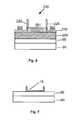
FIG. 8 shows a symbolic view of a processor containing at least one chip which contains at least one sectional FET.FIG. 1 shows schematic cross sectional views of the body regions of various embodiments of sectional FETs. In general, a Field-Effect-Transistor (FET) is a device where the current flow is controlled by a gate electrode between two parts of the device, the source and the drain. The gate electrode exerts its control with a field over the body of the device. The body is between the source and the drain and the gate electrode engages the body over a surface, or face. The gate electrode typically, but not necessarily, is separated form the face, or faces, of the body by a gate dielectric. The body of the FET is a crystalline semiconductor, where the face upon which the gate electrode exerts its field can form a conductive channel between the source and the drain. The common FET as known in the art has a single horizontal body section engaged by the gate electrode. The present disclosure contemplates FET devices with multiple body sections, having both horizontally oriented and vertically oriented sections. The orientations of the sections are with reference to a plane which contains the source and the drain. The sectional FETs of this disclosure are representatives of a so called semiconductor-on-insulator technology, where the device is disposed over an insulator. The dominant semiconductor of the microelectronic arts is silicon, and term silicon-on-insulator (SOI) is also commonly used to define devices disposed over insulators.- A representative embodiment of the body of a sectional FET is shown in cross section in
FIG. 1A . Thebody 10 is a crystalline semiconductor material. In a representative embodiment the crystalline semiconductor material of thebody 10 belongs in the broad category of Si based materials. In microelectronics technology the material that has progressed the farthest in miniaturization is silicon (Si). Si based materials are various alloys of Si in the same basic technological content as Si. One such Si based material of importance for microelectronics is the silicon-germanium (SiGe) alloy. In a representative embodiment the crystalline semiconductor material of thebody 10 is essentially Si. One skilled in the art, however, would recognize that other semiconductors materials beyond Si and SiGe, such as III-V alloys, can also be contemplated. According to the teaching of this disclosure the sectional FET body has at least one vertically oriented section and at least one horizontally oriented section. InFIG. 1A the body incross section 10 has two vertically orientedsections 11, and one horizontally orientedsection 12. Vertically orientedsections 11 each comprise two opposingfaces section 12, as typically all horizontally oriented sections comprise atop face 32, and abottom face 42. Thebottom face 42 is interfacing with an insulatingsurface 21. The vertically oriented sections have afirst height 77, and afirst width 16. The horizontally orientedsection 12 has afirst thickness 22. In a representative embodiment thefirst height 77 is between about 30 nm and 150 nm. In a representative embodiment thefirst thickness 22 is between about 2 nm and 50 nm. This disclosure teaches narrow width for the at least one vertically orientedsection 11 of the sectional FET, such that thefirst width 16 is less than the minimum linewidth of the technology in which the FET is manufactured in. At any given point in the state of the art of semiconductor processing there is a minimum feature size that the technology is capable of achieving by lithography. This linewidth is customarily given as the name of the technology of a given generation, for instance: “a 0.25 μm technology” etc. Thefirst width 16 of the vertically oriented section is less than this minimum lithographic linewidth, independently in which particular technology generation the sectional FET is produced in, since thefirst width 16 is not produced by lithography. FIG. 1B shows exemplary embodiments ofsectional FET bodies 10 with differing number of horizontally oriented12 and vertically oriented11 sections. The figure, which shows threediffering bodies 10, is only for representative purposes and should not be interpreted restrictively. The teaching of the disclosure is capable to produce any number of horizontally oriented and vertically oriented sections. The insulatingsurface 21 typically is a top surface of aninsulator layer 90, on which the crystalline semiconductor material of the sectional FET body is disposed. Theinsulator layer 90 is typically disposed over asubstrate 91. In a representative embodiment theinsulator layer 90 is SiO2, and thesubstrate 91 is a Si wafer. Typically the sectional FET is produced in SOI technology, where a so called buried oxide (SiO2) is disposed over a Si substrate, and an SOI silicon layer is disposed over the buried oxide. In a representative embodiment the sectional FET is fabricated in an SOI layer.FIG. 1C shows exemplary embodiments of thesectional FET bodies 10 ofFIG. 1B with agate electrode 50 engaging the top face32 (indicated inFIG. 1A ) of the at least one horizontally orientedsection 12 and the opposing faces31 and41 (indicated inFIG. 1A ) of the at least one vertically orientedsection 11. The sectional devices provide a combination of two types of high performance devices. The vertically orientedsections 11 are similar to the so called FinFETs, or vertical devices, while the horizontally orientedsection 12 is similar to an ultra thin bodied planar device. If final devices should be built as fully depleted silicon-on-insulator (FDSOI), FETs, the typicalfirst width 16 of the vertically orientedsections 11, is about twice of thefirst thickness 22 of the horizontally orientedsection 12. In this disclosure all the faces of all of the sections are engaged bysingle gate electrode 50, leading to low capacitance and high current driving capability for the sectional devices. The FET on the left ofFIG. 1C shows one horizontally orientedsection 12 situated between two vertically orientedsections 11, with the gate electrode engaging simultaneously four vertically oriented faces and one horizontally oriented face, for a total of five. Such a device can be called a pentagate FET.- In representative embodiments the body of the sectional FETs shown in
FIG. 1 are fully depleted., which means the body does not have mobile charge carriers, except for those induced by the gate electrode in the channel. In SOI technologies for the usual planar devices whether a body is depleted or not depends of the doping level of the body and the thickness of the body. For the vertically oriented sections, again beside the doping level, thefirst width 16, the distance between the opposing faces engaged by the gate electrode, of the vertical section is the one that matters from the point of view of depletion. In the sectional FETs of the present disclosure one can make the first thickness of the horizontally orientedsection 22 thin enough to be fully depleted. Since the vertical sections are not constrained by lithography limitations they too can be made sufficiently narrow, that they can become fully depleted. SOI devices. Fully depleted bodies have numerous advantages, as it is known by those ordinarily skilled in the art. FIG. 2 shows a schematic top view and cross sectional views of a sectional FET. InFIG. 2A thesectional FET 100 comprise the source/drain 110, thegate 50, and the body10 (visible only inFIG. 2C ) under the gate electrode. During the fabrication of the sectional FET one produces a certain structure, which we callkernel 15. (The word kernel expresses the role this structure plays.) Thekernel 15 comprises the body: as that portion of the kernel which is engaged by the gate electrode becomes thebody 10. As produced, thekernel 15 has essentially the same cross sectional dimensions as the body. In portions other than the body, thekernel 15 becomes a component of the source/drain 110. For source/drain it is desirable to have as low resistance as possible, and to have enough bulk for easy wiring contacts, and/or silicidation. Such properties call for more material than was produced in the kernel, since the primary concern there was to comply with the requirements for the body. Therefore, in representative embodiments of the sectional FETs, for the purpose of turning portions of the kernel—those portions that do not form the body—into an improved source/drain 110, athird layer 111 is deposited over those kernel portions. InFIG. 2A the rough location of thekernel 15 is indicated only by broken lines, since in the source/drain regions thekernel 15 is typically underneath thethird layer 111 and not visible in a top view. In a representative embodiment the kernel is a Si based material, typically Si, and thethird layer 111 consists of the same material as thekernel 15. Accordingly, in a representative embodiment one selects thethird layer 111 to consist of the same crystalline semiconductor material as thekernel 15, typically Si, and selects the depositing to be carried out by selective epitaxy over the kernel in the source/drain 110. This result can be seen inFIG. 2B which is a cross section ofFIG. 2A along the dotted line “b”. Thekernel 15 in the source/drain 110 has the same cross sectional features as thebody 10, but it is covered bythird layer 111. In the case of an epitaxial deposition, thethird layer 111 would be essentially indistinguishable from thekernel 15. Since in such embodiments thekernel 15 and thethird layer 111 together make up the source/drain 110, theminimum thickness 113 of the source/drain is larger than thefirst thickness 22 of the body's horizontally oriented section. Themaximum thickness 112 of the source/drain is at least as large as thefirst height 77 of the body's vertical section. Themaximum thickness 112 of the source/drain may also be over thefirst height 77, as this is depending on the deposition technique and further processing. One skilled in the art would understand the tradeoffs involved in the question of increasing themaximum thickness 112 of the source/drain 110FIG. 2C is a cross sectional view of thegate 50 and thebody 10, (similar toFIG. 1C ) along the dotted line “a” ofFIG. 2A . Thegate 50 is engaging the various faces of the at least onevertical section 11 and the at least one horizontally orientedsection 12. As is clear fromFIG. 2C , the body portion of the kernel is not covered bythird layer 111.- FIGS.3 to7 show stages of a representative method of fabrication of a sectional FET. In general the present disclosure teaches that first a formation of walls and layers is fabricated on top of a SOI layer and then this formation is transferred down—with the help of various etchings—into the SOI layer, forming the kernel, which kernel is then the foundation for building up the
sectional FET 100. FIG. 3 shows, in a schematic cross section, a stage in an exemplary embodiment of the method for fabricating a sectional FET, at a step along the method for creating the formation310 (shown inFIG. 6 ). Aninsulator layer 90 is disposed over asubstrate 91. In a representative embodiment theinsulator layer 90 is a buried SiO2, and thesubstrate 91 is a Si wafer. Disposed over theinsulator 90 is afirst layer 200 of acrystalline semiconductor material 200. Thisfirst layer 200 is the one into which thekernel 15 comprising the body of the sectional FET will be etched into. In a representative embodiment the first layer is Si with a thickness of between about 30 nm and 150 nm. Disposed on top of thefirst layer 200 issecond layer 210, in an exemplary embodiment a SiO2layer. This SiO2layer210 can be disposed over the first layer by any of the known methods in the art. Ontolayer 210, a fourth layer is deposited and then patterned230, (shown after the patterning). In a representative embodiment thefourth layer 230 is an amorphous Si layer, in the range of about 70 nm-120 nm thickness, typically deposited by low pressure chemical vapor deposition (LPCVD) or rapid thermal CVD (RTCVD).FIG. 4 shows in a schematic cross section the fabrication at a stage when a sidewall creation process has been completed, involving thefourth layer 230. Thesidewall 220 can be produced by standard spacer-etch techniques, well known in the electronic processing arts. In a representative embodiment thiswall 220 is made of silicon-nitride (Si3N4). The width of thewall 220 is independent of lithographic capabilities of the processing technology, since no patterning step is involved in its formation.FIG. 5 shows schematically an top view of the method at the stage after thewall 220 formation. There exists at least one island of thefourth layer 230; in the figure for illustration purposes three islands are shown. Thesefourth layer islands 230 are surrounded by thewall 220. A large part of the visible surface is thesecond layer 210.FIG. 5 shows how the surface is divided into regions of inside the wall and of outside the wall. Even though there maybe more than one island involved in the fabrication of a single kernel, one can talk of a single wall, with an inside301 and an outside302. If there is only oneisland 230, the inside301 is self evident, being theisland region 230. If the kernel to be fabricated needs more than one island—which is the case when one desires to have more than two vertical sections in the final sectional FET—at this stage one has to lithographically define the extent of the kernel, which region, as an example, inFIG. 5 is shown by dottedlines 303. In this case the inside of thewall 301 is defined as the area inside the dottedlines 303, and the outside of thewall 302 is defined as the area outside the dottedline 303. For the case of multiple islands in order to protect thesecond layer 210 in the whole of the inside301, one deposits a fifth layer ofmaterial 240. Thisfifth layer 240 in an exemplary embodiment can be of the same material as thefourth layer 230, typically amorphous Si. With the protection of thefifth layer 240 in place one can etch thesecond layer 210 outside the wall, without effecting thesecond layer 210 inside the wall. If the kernel is in need of no more than two vertical sections, then oneisland 230 is sufficient, and there is no need to deposit thefifth layer 240, since then thefourth layer 230 which was used to create thewall 220 automatically protectslayer 210 in the inside301.FIG. 6 shows in a schematic cross section the method once theformation 310 has been completed. The formation has awall 220, typically silicon-nitride (Si3N4), and asecond layer 210, typically SiO2, the second layer is disposed over thefirst layer 200, typically Si. Thewall 220 is disposed on thesecond layer 210, and the wall has an inside301 and an outside302. Thesecond layer 210 is thinner in the outside302 than in the inside301. In a representative embodiment, from the state depicted onFIG. 4 one can arrive at having fabricated the formation as shown inFIG. 6 , by executing the following steps. An etching step to partially remove the SiO2layer210 over the outside302. Such etching steps are well known in the art, either in a dry etch format, or by a wet etch. If there is only one island involved, one can combine this etching step of partially removing theoxide 210 from the outside with the earlier wall fabrication step of etching the wall material. Next, one etches, again with standard methods, to leave only the silicon-nitride wall 220 and the SiO2layer over the first material. This step involves the removal of theamorphous Si layer 230, and if present, the removal of thefifth layer 240. Removal offifth layer 240 usually is not problematic since usually thefifth layer 240 is the same material as the fourth230, namely, amorphous Si. When these two etching steps are done theformation 16 is ready.FIG. 7 shows in a schematic cross section the method once thekernel 15 has been completed. Thekernel 15 consists of thecrystalline semiconductor material 200, and thekernel 15 comprises theFET body 10, which body has at least one vertically orientedsection 11 and at least one horizontally orientedsection 12.- Commencing at the state depicted in
FIG. 6 , theformation 310—the Si3N4wall220, and thicker SiO2in the inside301 an the thinner SiO2in the outside302—has to be transferred into thefirst layer 200. The initial step to achieve this aim is performing a first etch to completely remove thesecond layer 210 from the outside302, and to partially remove thesecond layer 210 from the inside301. The first etch in an exemplary embodiment is a uniform plasma etch. Typically one uses a bromine based plasma, such HBr mixed with a small flow of oxygen. For a representative embodiment when thesecond layer 210 is a thermally deposited oxide (TEOS), typical parameters for the first etch are: a flow rate of about between 50-300 Standard Cubic Centimeter per Minute (SCCM) of HBr, and of about between 0-5 SCCM of O2; a top rf source power of about between 200 W-350 W, bottom electrode (wafer) rf power: between about 150 W-350 W; pressure: between about 3-6 mTorr. Processing time is controlled by detecting complete removal of material on the outside, for instance optical emission spectroscopic (OES) end-point traces in the outside302. The ion assistant reactive ion etching regime of the first etch ensures an etch rate of TEOS in the outside302 which is similar, or slightly faster than the etch rate of TEOS in the inside301. Accordingly, after fully removing TEOS in the outside302, there is still a thin layer of TEOS left in the inside301. - Next, a using a second etch one fully removes the
second layer 210, typically TEOS, in the inside301, and partially removes thefirst layer 200, typically Si, in the outside302. For a representative embodiment when thesecond layer 210 is TEOS, and thefirst layer 200 is Si, typical parameters for the plasma etch—the second etch—are: a flow rate of about between 150-300 SCCM of HBr; a top rf source power of about between 150 W-350 W, bottom electrode (wafer) rf power: between about 150 W-350 W; pressure: between about 3-6 mTorr. Etching time is of a few seconds, typically between about 7 sec and 15 sec. - Next, a using a third etch one fully removes the
first layer 200, typically Si, in the outside302. The duration of the third etch is again controlled by detecting complete removal of material on the outside, such as by OES end-point traces in the outside302. When theSi 200 is fully removed in the outside302, a layer of Si still remains in the inside, since after the second etch theSi 200 was thicker in the inside301 than in the outside302. For a representative embodiment when thefirst layer 200 is Si, typical parameters for the plasma etch—the third etch—are: a flow rate of about between 100-350 SCCM of HBr, and of about between 0-5 SCCM of O2; a top rf source power of about between 80 W-250 W, bottom electrode (wafer) rf power: between about 10 W-100 W; pressure: between about 5-10 mTorr. - Having finished with these three etches one has transferred the
formation 310 into thefirst layer 200. After removing the remaining silicon-nitride wall 220 and remaining TEOS mask layer210 (which was under the wall), usually by wet etching, the result is thekernel 15. During the various etches thefirst layer 200 under the Si3N4wall220 was protected, with the result that it yields the vertically oriented sections for the body. - Optionally, before removing the silicon-nitride wall, one can execute a fourth etch to control the thickness of the
first layer 200 in the inside301, in order to control thefirst thickness 22 of the horizontally oriented sections for the body. For an exemplary embodiment when thefirst layer 200 is Si, typical parameters for the fourth etch are: a flow rate of about between 100-350 SCCM of HBr, of about between 0-5 SCCM of O2, and of about between 100-350 SCCM of He; a top rf source power of about between 100 W-400 W, bottom electrode (wafer) rf power: between about 10 W-100 W; pressure: between about 20-100 mTorr. - If one desires, after the described etching steps took place, part of the kernel can be removed with standard etching techniques known in the art. This could be the case, for instance, if an odd number of vertically oriented sections, or an even number of horizontally oriented sections are needed. Or, one may be in need of various complicated layout shapes, which are best achieved by fabricating a kernel with several differently placed islands, and then etching away unwanted parts.
- Having finished with the
kernel 15, further processing for the sectional FET follows mainly along the lines of established FET processing. The exceptions are as follows. Given the shape of thegate electrode 50, which has to engage faces of various orientations extra care is needed during its deposition. Also, as discussed in relation toFIG. 2 , athird layer 111 is deposited over thekernel 15 for the source/drain 110. Thethird layer 111 is typically Si and it is deposited over the Si of the kernel by selective epitaxy. - The fabricated segmented FET thus combines FinFET type devices with fully depleted planar devices. This combination allows device width control with FinFET type devices. The segmented FET device gives high current drive for a given layout area.
FIG. 8 shows a symbolic view of a processor containing at least one chip which contains at least one sectional FET. Such aprocessor 900 has at least onechip 901, which contains at least onesectional FET 100 of the present invention. Theprocessor 900 can be any processor which can benefit from thesectional FET device 100. These devices form part of the processor in their multitude on one ormore chips 901. Representative embodiments of processors manufactured with sectional FET devices are digital processors, typically found in the central processing complex of computers; mixed digital/analog processors, which benefit significantly from the high performance of the sectional FET devices; and in general any communication processor, such as modules connecting memories to processors, routers, radar systems, high performance video-telephony, game modules, and others.- Many modifications and variations of the present invention are possible in light of the above teachings, and could be apparent for those skilled in the art. The scope of the invention is defined by the appended claims.
Claims (31)
Priority Applications (8)
| Application Number | Priority Date | Filing Date | Title |
|---|---|---|---|
| US10/732,322US7388258B2 (en) | 2003-12-10 | 2003-12-10 | Sectional field effect devices |
| CNB2007101092000ACN100524667C (en) | 2003-12-10 | 2004-11-02 | Sectional field effect transistor making method |
| CNB2004100901358ACN100382331C (en) | 2003-12-10 | 2004-11-02 | Segmented Field Effect Transistor and Method of Manufacturing the Same |
| KR1020040091550AKR100627955B1 (en) | 2003-12-10 | 2004-11-10 | Sectional Field Effect Devices and Method of Fabrication |
| TW093134801ATWI318795B (en) | 2003-12-10 | 2004-11-12 | Sectional field effect devices and method of fabrication |
| JP2004353555AJP4549829B2 (en) | 2003-12-10 | 2004-12-07 | Manufacturing method of unit type field effect device |
| US11/433,806US7413941B2 (en) | 2003-12-10 | 2006-05-13 | Method of fabricating sectional field effect devices |
| US12/142,849US7659153B2 (en) | 2003-12-10 | 2008-06-20 | Sectional field effect devices and method of fabrication |
Applications Claiming Priority (1)
| Application Number | Priority Date | Filing Date | Title |
|---|---|---|---|
| US10/732,322US7388258B2 (en) | 2003-12-10 | 2003-12-10 | Sectional field effect devices |
Related Child Applications (1)
| Application Number | Title | Priority Date | Filing Date |
|---|---|---|---|
| US11/433,806DivisionUS7413941B2 (en) | 2003-12-10 | 2006-05-13 | Method of fabricating sectional field effect devices |
Publications (2)
| Publication Number | Publication Date |
|---|---|
| US20050127362A1true US20050127362A1 (en) | 2005-06-16 |
| US7388258B2 US7388258B2 (en) | 2008-06-17 |
Family
ID=34652851
Family Applications (3)
| Application Number | Title | Priority Date | Filing Date |
|---|---|---|---|
| US10/732,322Expired - LifetimeUS7388258B2 (en) | 2003-12-10 | 2003-12-10 | Sectional field effect devices |
| US11/433,806Expired - LifetimeUS7413941B2 (en) | 2003-12-10 | 2006-05-13 | Method of fabricating sectional field effect devices |
| US12/142,849Expired - LifetimeUS7659153B2 (en) | 2003-12-10 | 2008-06-20 | Sectional field effect devices and method of fabrication |
Family Applications After (2)
| Application Number | Title | Priority Date | Filing Date |
|---|---|---|---|
| US11/433,806Expired - LifetimeUS7413941B2 (en) | 2003-12-10 | 2006-05-13 | Method of fabricating sectional field effect devices |
| US12/142,849Expired - LifetimeUS7659153B2 (en) | 2003-12-10 | 2008-06-20 | Sectional field effect devices and method of fabrication |
Country Status (5)
| Country | Link |
|---|---|
| US (3) | US7388258B2 (en) |
| JP (1) | JP4549829B2 (en) |
| KR (1) | KR100627955B1 (en) |
| CN (2) | CN100524667C (en) |
| TW (1) | TWI318795B (en) |
Cited By (37)
| Publication number | Priority date | Publication date | Assignee | Title |
|---|---|---|---|---|
| US20040094807A1 (en)* | 2002-08-23 | 2004-05-20 | Chau Robert S. | Tri-gate devices and methods of fabrication |
| US20050148137A1 (en)* | 2003-12-30 | 2005-07-07 | Brask Justin K. | Nonplanar transistors with metal gate electrodes |
| US20050158970A1 (en)* | 2004-01-16 | 2005-07-21 | Robert Chau | Tri-gate transistors and methods to fabricate same |
| US20050193143A1 (en)* | 2003-12-30 | 2005-09-01 | Meyers Brian R. | Framework for user interaction with multiple network devices |
| US20050218438A1 (en)* | 2004-03-31 | 2005-10-06 | Nick Lindert | Bulk non-planar transistor having strained enhanced mobility and methods of fabrication |
| US20060033095A1 (en)* | 2004-08-10 | 2006-02-16 | Doyle Brian S | Non-planar pMOS structure with a strained channel region and an integrated strained CMOS flow |
| US20060043502A1 (en)* | 2003-11-26 | 2006-03-02 | International Business Machines Corporation | Structure and method to fabricate finfet devices |
| US20060063332A1 (en)* | 2004-09-23 | 2006-03-23 | Brian Doyle | U-gate transistors and methods of fabrication |
| US20060068591A1 (en)* | 2004-09-29 | 2006-03-30 | Marko Radosavljevic | Fabrication of channel wraparound gate structure for field-effect transistor |
| US20060128131A1 (en)* | 2004-09-29 | 2006-06-15 | Chang Peter L | Independently accessed double-gate and tri-gate transistors in same process flow |
| US20060138552A1 (en)* | 2004-09-30 | 2006-06-29 | Brask Justin K | Nonplanar transistors with metal gate electrodes |
| US20060157687A1 (en)* | 2005-01-18 | 2006-07-20 | Doyle Brian S | Non-planar MOS structure with a strained channel region |
| US20060172497A1 (en)* | 2003-06-27 | 2006-08-03 | Hareland Scott A | Nonplanar semiconductor device with partially or fully wrapped around gate electrode and methods of fabrication |
| US20060186484A1 (en)* | 2005-02-23 | 2006-08-24 | Chau Robert S | Field effect transistor with narrow bandgap source and drain regions and method of fabrication |
| US20060214231A1 (en)* | 2004-10-25 | 2006-09-28 | Uday Shah | Nonplanar device with thinned lower body portion and method of fabrication |
| US20060286755A1 (en)* | 2005-06-15 | 2006-12-21 | Brask Justin K | Method for fabricating transistor with thinned channel |
| US20070001219A1 (en)* | 2005-06-30 | 2007-01-04 | Marko Radosavljevic | Block contact architectures for nanoscale channel transistors |
| WO2007036874A1 (en)* | 2005-09-28 | 2007-04-05 | Nxp B.V. | Finfet-based non-volatile memory device |
| US20070090416A1 (en)* | 2005-09-28 | 2007-04-26 | Doyle Brian S | CMOS devices with a single work function gate electrode and method of fabrication |
| US20070093010A1 (en)* | 2005-10-25 | 2007-04-26 | Leo Mathew | Method of making an inverted-T channel transistor |
| US20070093054A1 (en)* | 2005-10-25 | 2007-04-26 | Min Byoung W | Multiple device types including an inverted-T channel transistor and method therefor |
| US20070148837A1 (en)* | 2005-12-27 | 2007-06-28 | Uday Shah | Method of fabricating a multi-cornered film |
| US7241653B2 (en) | 2003-06-27 | 2007-07-10 | Intel Corporation | Nonplanar device with stress incorporation layer and method of fabrication |
| US20070158762A1 (en)* | 2006-01-11 | 2007-07-12 | Anderson Brent A | Low-capacitance contact for long gate-length devices with small contacted pitch |
| US20070238273A1 (en)* | 2006-03-31 | 2007-10-11 | Doyle Brian S | Method of ion implanting for tri-gate devices |
| US7402875B2 (en) | 2005-08-17 | 2008-07-22 | Intel Corporation | Lateral undercut of metal gate in SOI device |
| US7479421B2 (en) | 2005-09-28 | 2009-01-20 | Intel Corporation | Process for integrating planar and non-planar CMOS transistors on a bulk substrate and article made thereby |
| US20090065869A1 (en)* | 2007-09-10 | 2009-03-12 | Kabushiki Kaisha Toshiba | Semiconductor device |
| US20090108353A1 (en)* | 2007-10-31 | 2009-04-30 | Advanced Micro Devices, Inc. | Finfet structure and methods |
| US7547637B2 (en) | 2005-06-21 | 2009-06-16 | Intel Corporation | Methods for patterning a semiconductor film |
| US7579280B2 (en) | 2004-06-01 | 2009-08-25 | Intel Corporation | Method of patterning a film |
| US20100065888A1 (en)* | 2004-06-30 | 2010-03-18 | Shaheen Mohamad A | High mobility tri-gate devices and methods of fabrication |
| US7879675B2 (en) | 2005-03-14 | 2011-02-01 | Intel Corporation | Field effect transistor with metal source/drain regions |
| US7989280B2 (en) | 2005-11-30 | 2011-08-02 | Intel Corporation | Dielectric interface for group III-V semiconductor device |
| US8362566B2 (en) | 2008-06-23 | 2013-01-29 | Intel Corporation | Stress in trigate devices using complimentary gate fill materials |
| US8617945B2 (en) | 2006-08-02 | 2013-12-31 | Intel Corporation | Stacking fault and twin blocking barrier for integrating III-V on Si |
| US11715796B2 (en) | 2021-03-12 | 2023-08-01 | Kabushiki Kaisha Toshiba | High frequency transistor |
Families Citing this family (18)
| Publication number | Priority date | Publication date | Assignee | Title |
|---|---|---|---|---|
| KR100585178B1 (en)* | 2005-02-05 | 2006-05-30 | 삼성전자주식회사 | A semiconductor device comprising a metal FET having a metal gate electrode, and a manufacturing method thereof |
| JP2007173326A (en)* | 2005-12-19 | 2007-07-05 | Korea Advanced Inst Of Sci Technol | Field effect transistor having channel comprising silicon fin and silicon body and method of manufacturing |
| KR100756809B1 (en) | 2006-04-28 | 2007-09-07 | 주식회사 하이닉스반도체 | Semiconductor device and manufacturing method thereof |
| US7517764B2 (en)* | 2006-06-29 | 2009-04-14 | International Business Machines Corporation | Bulk FinFET device |
| KR100954116B1 (en)* | 2006-11-06 | 2010-04-23 | 주식회사 하이닉스반도체 | Method of forming recess pattern in semiconductor device |
| US8207038B2 (en)* | 2010-05-24 | 2012-06-26 | International Business Machines Corporation | Stressed Fin-FET devices with low contact resistance |
| US20110291188A1 (en)* | 2010-05-25 | 2011-12-01 | International Business Machines Corporation | Strained finfet |
| US8389416B2 (en)* | 2010-11-22 | 2013-03-05 | Tokyo Electron Limited | Process for etching silicon with selectivity to silicon-germanium |
| US8726220B2 (en)* | 2011-04-29 | 2014-05-13 | Taiwan Semiconductor Manufacturing Company, Ltd. | System and methods for converting planar design to FinFET design |
| US8692291B2 (en) | 2012-03-27 | 2014-04-08 | International Business Machines Corporation | Passive devices for FinFET integrated circuit technologies |
| CN103426755B (en)* | 2012-05-14 | 2015-12-09 | 中芯国际集成电路制造(上海)有限公司 | Semiconductor device and forming method thereof |
| US8956932B2 (en)* | 2013-02-25 | 2015-02-17 | International Business Machines Corporation | U-shaped semiconductor structure |
| CN104701184A (en)* | 2015-03-20 | 2015-06-10 | 上海华力微电子有限公司 | Method for forming field emission transistor with multi-fin structure |
| US9293374B1 (en) | 2015-06-12 | 2016-03-22 | International Business Machines Corporation | Self-aligned low defect segmented III-V finFET |
| CN109087865A (en)* | 2017-06-14 | 2018-12-25 | 中芯国际集成电路制造(上海)有限公司 | A kind of manufacturing method of semiconductor devices |
| CN109285889B (en)* | 2017-07-20 | 2021-07-13 | 中芯国际集成电路制造(上海)有限公司 | Semiconductor structure and method of forming the same |
| CN109285876B (en)* | 2017-07-20 | 2021-08-06 | 中芯国际集成电路制造(上海)有限公司 | Semiconductor structure and method of forming the same |
| KR102532118B1 (en) | 2018-03-20 | 2023-05-11 | 삼성전자주식회사 | Semiconductor device and method for fabricating the same |
Citations (11)
| Publication number | Priority date | Publication date | Assignee | Title |
|---|---|---|---|---|
| US4907053A (en)* | 1983-08-25 | 1990-03-06 | Tadahiro Ohmi | Semiconductor integrated circuit |
| US5136350A (en)* | 1989-09-28 | 1992-08-04 | Oki Electric Industry Co., Ltd. | Semiconductor mosfet having a projecting T-shaped portion |
| US5225701A (en)* | 1989-12-15 | 1993-07-06 | Mitsubishi Denki Kabushiki Kaisha | Vertical silicon-on-insulator (SOI) MOS type field effect transistor |
| US6228691B1 (en)* | 1999-06-30 | 2001-05-08 | Intel Corp. | Silicon-on-insulator devices and method for producing the same |
| US6483156B1 (en)* | 2000-03-16 | 2002-11-19 | International Business Machines Corporation | Double planar gated SOI MOSFET structure |
| US6541810B2 (en)* | 2001-06-29 | 2003-04-01 | International Business Machines Corporation | Modified vertical MOSFET and methods of formation thereof |
| US6562665B1 (en)* | 2000-10-16 | 2003-05-13 | Advanced Micro Devices, Inc. | Fabrication of a field effect transistor with a recess in a semiconductor pillar in SOI technology |
| US6716686B1 (en)* | 2003-07-08 | 2004-04-06 | Advanced Micro Devices, Inc. | Method for forming channels in a finfet device |
| US6750487B2 (en)* | 2002-04-11 | 2004-06-15 | International Business Machines Corporation | Dual double gate transistor |
| US6800910B2 (en)* | 2002-09-30 | 2004-10-05 | Advanced Micro Devices, Inc. | FinFET device incorporating strained silicon in the channel region |
| US20050023619A1 (en)* | 2003-07-31 | 2005-02-03 | Orlowski Marius K. | Method of forming a transistor having multiple channels and structure thereof |
Family Cites Families (8)
| Publication number | Priority date | Publication date | Assignee | Title |
|---|---|---|---|---|
| JPH04268767A (en) | 1991-02-25 | 1992-09-24 | Fujitsu Ltd | semiconductor equipment |
| JP2571004B2 (en) | 1993-12-22 | 1997-01-16 | 日本電気株式会社 | Thin film transistor |
| US7163864B1 (en)* | 2000-10-18 | 2007-01-16 | International Business Machines Corporation | Method of fabricating semiconductor side wall fin |
| US6475890B1 (en)* | 2001-02-12 | 2002-11-05 | Advanced Micro Devices, Inc. | Fabrication of a field effect transistor with an upside down T-shaped semiconductor pillar in SOI technology |
| US6798017B2 (en)* | 2001-08-31 | 2004-09-28 | International Business Machines Corporation | Vertical dual gate field effect transistor |
| CN1193432C (en)* | 2003-02-14 | 2005-03-16 | 中国科学院上海微系统与信息技术研究所 | Structure and realization method for reducing the source-drain series resistance of silicon transistor on insulator |
| US6943405B2 (en)* | 2003-07-01 | 2005-09-13 | International Business Machines Corporation | Integrated circuit having pairs of parallel complementary FinFETs |
| US20060084243A1 (en)* | 2004-10-20 | 2006-04-20 | Ying Zhang | Oxidation sidewall image transfer patterning method |
- 2003
- 2003-12-10USUS10/732,322patent/US7388258B2/ennot_activeExpired - Lifetime
- 2004
- 2004-11-02CNCNB2007101092000Apatent/CN100524667C/ennot_activeExpired - Lifetime
- 2004-11-02CNCNB2004100901358Apatent/CN100382331C/ennot_activeExpired - Lifetime
- 2004-11-10KRKR1020040091550Apatent/KR100627955B1/ennot_activeExpired - Fee Related
- 2004-11-12TWTW093134801Apatent/TWI318795B/ennot_activeIP Right Cessation
- 2004-12-07JPJP2004353555Apatent/JP4549829B2/ennot_activeExpired - Fee Related
- 2006
- 2006-05-13USUS11/433,806patent/US7413941B2/ennot_activeExpired - Lifetime
- 2008
- 2008-06-20USUS12/142,849patent/US7659153B2/ennot_activeExpired - Lifetime
Patent Citations (11)
| Publication number | Priority date | Publication date | Assignee | Title |
|---|---|---|---|---|
| US4907053A (en)* | 1983-08-25 | 1990-03-06 | Tadahiro Ohmi | Semiconductor integrated circuit |
| US5136350A (en)* | 1989-09-28 | 1992-08-04 | Oki Electric Industry Co., Ltd. | Semiconductor mosfet having a projecting T-shaped portion |
| US5225701A (en)* | 1989-12-15 | 1993-07-06 | Mitsubishi Denki Kabushiki Kaisha | Vertical silicon-on-insulator (SOI) MOS type field effect transistor |
| US6228691B1 (en)* | 1999-06-30 | 2001-05-08 | Intel Corp. | Silicon-on-insulator devices and method for producing the same |
| US6483156B1 (en)* | 2000-03-16 | 2002-11-19 | International Business Machines Corporation | Double planar gated SOI MOSFET structure |
| US6562665B1 (en)* | 2000-10-16 | 2003-05-13 | Advanced Micro Devices, Inc. | Fabrication of a field effect transistor with a recess in a semiconductor pillar in SOI technology |
| US6541810B2 (en)* | 2001-06-29 | 2003-04-01 | International Business Machines Corporation | Modified vertical MOSFET and methods of formation thereof |
| US6750487B2 (en)* | 2002-04-11 | 2004-06-15 | International Business Machines Corporation | Dual double gate transistor |
| US6800910B2 (en)* | 2002-09-30 | 2004-10-05 | Advanced Micro Devices, Inc. | FinFET device incorporating strained silicon in the channel region |
| US6716686B1 (en)* | 2003-07-08 | 2004-04-06 | Advanced Micro Devices, Inc. | Method for forming channels in a finfet device |
| US20050023619A1 (en)* | 2003-07-31 | 2005-02-03 | Orlowski Marius K. | Method of forming a transistor having multiple channels and structure thereof |
Cited By (130)
| Publication number | Priority date | Publication date | Assignee | Title |
|---|---|---|---|---|
| US7504678B2 (en) | 2002-08-23 | 2009-03-17 | Intel Corporation | Tri-gate devices and methods of fabrication |
| US20040094807A1 (en)* | 2002-08-23 | 2004-05-20 | Chau Robert S. | Tri-gate devices and methods of fabrication |
| US7358121B2 (en) | 2002-08-23 | 2008-04-15 | Intel Corporation | Tri-gate devices and methods of fabrication |
| US20070281409A1 (en)* | 2002-08-23 | 2007-12-06 | Yuegang Zhang | Multi-gate carbon nano-tube transistors |
| US7368791B2 (en) | 2002-08-23 | 2008-05-06 | Intel Corporation | Multi-gate carbon nano-tube transistors |
| US20050199950A1 (en)* | 2002-08-23 | 2005-09-15 | Chau Robert S. | Tri-gate devices and methods of fabrication |
| US7427794B2 (en) | 2002-08-23 | 2008-09-23 | Intel Corporation | Tri-gate devices and methods of fabrication |
| US7514346B2 (en) | 2002-08-23 | 2009-04-07 | Intel Corporation | Tri-gate devices and methods of fabrication |
| US7560756B2 (en) | 2002-08-23 | 2009-07-14 | Intel Corporation | Tri-gate devices and methods of fabrication |
| US20070034972A1 (en)* | 2002-08-23 | 2007-02-15 | Chau Robert S | Tri-gate devices and methods of fabrication |
| US20060228840A1 (en)* | 2002-08-23 | 2006-10-12 | Chau Robert S | Tri-gate devices and methods of fabrication |
| US7241653B2 (en) | 2003-06-27 | 2007-07-10 | Intel Corporation | Nonplanar device with stress incorporation layer and method of fabrication |
| US7456476B2 (en) | 2003-06-27 | 2008-11-25 | Intel Corporation | Nonplanar semiconductor device with partially or fully wrapped around gate electrode and methods of fabrication |
| US8405164B2 (en) | 2003-06-27 | 2013-03-26 | Intel Corporation | Tri-gate transistor device with stress incorporation layer and method of fabrication |
| US20060172497A1 (en)* | 2003-06-27 | 2006-08-03 | Hareland Scott A | Nonplanar semiconductor device with partially or fully wrapped around gate electrode and methods of fabrication |
| US7820513B2 (en) | 2003-06-27 | 2010-10-26 | Intel Corporation | Nonplanar semiconductor device with partially or fully wrapped around gate electrode and methods of fabrication |
| US7714397B2 (en) | 2003-06-27 | 2010-05-11 | Intel Corporation | Tri-gate transistor device with stress incorporation layer and method of fabrication |
| US8273626B2 (en) | 2003-06-27 | 2012-09-25 | Intel Corporationn | Nonplanar semiconductor device with partially or fully wrapped around gate electrode and methods of fabrication |
| US7470629B2 (en) | 2003-11-26 | 2008-12-30 | International Business Machines Corporation | Structure and method to fabricate finfet devices |
| US20060043502A1 (en)* | 2003-11-26 | 2006-03-02 | International Business Machines Corporation | Structure and method to fabricate finfet devices |
| US20050148137A1 (en)* | 2003-12-30 | 2005-07-07 | Brask Justin K. | Nonplanar transistors with metal gate electrodes |
| US7105390B2 (en) | 2003-12-30 | 2006-09-12 | Intel Corporation | Nonplanar transistors with metal gate electrodes |
| US20050193143A1 (en)* | 2003-12-30 | 2005-09-01 | Meyers Brian R. | Framework for user interaction with multiple network devices |
| US7624192B2 (en) | 2003-12-30 | 2009-11-24 | Microsoft Corporation | Framework for user interaction with multiple network devices |
| US20050156171A1 (en)* | 2003-12-30 | 2005-07-21 | Brask Justin K. | Nonplanar transistors with metal gate electrodes |
| US7329913B2 (en) | 2003-12-30 | 2008-02-12 | Intel Corporation | Nonplanar transistors with metal gate electrodes |
| US20050158970A1 (en)* | 2004-01-16 | 2005-07-21 | Robert Chau | Tri-gate transistors and methods to fabricate same |
| US7268058B2 (en) | 2004-01-16 | 2007-09-11 | Intel Corporation | Tri-gate transistors and methods to fabricate same |
| US7781771B2 (en) | 2004-03-31 | 2010-08-24 | Intel Corporation | Bulk non-planar transistor having strained enhanced mobility and methods of fabrication |
| US20050218438A1 (en)* | 2004-03-31 | 2005-10-06 | Nick Lindert | Bulk non-planar transistor having strained enhanced mobility and methods of fabrication |
| US7326634B2 (en) | 2004-03-31 | 2008-02-05 | Intel Corporation | Bulk non-planar transistor having strained enhanced mobility and methods of fabrication |
| US7579280B2 (en) | 2004-06-01 | 2009-08-25 | Intel Corporation | Method of patterning a film |
| US20100065888A1 (en)* | 2004-06-30 | 2010-03-18 | Shaheen Mohamad A | High mobility tri-gate devices and methods of fabrication |
| US8084818B2 (en) | 2004-06-30 | 2011-12-27 | Intel Corporation | High mobility tri-gate devices and methods of fabrication |
| US20060033095A1 (en)* | 2004-08-10 | 2006-02-16 | Doyle Brian S | Non-planar pMOS structure with a strained channel region and an integrated strained CMOS flow |
| US7348284B2 (en) | 2004-08-10 | 2008-03-25 | Intel Corporation | Non-planar pMOS structure with a strained channel region and an integrated strained CMOS flow |
| US7960794B2 (en) | 2004-08-10 | 2011-06-14 | Intel Corporation | Non-planar pMOS structure with a strained channel region and an integrated strained CMOS flow |
| GB2430805B (en)* | 2004-09-23 | 2009-04-29 | Intel Corp | U-gate transistors and methods of fabrication |
| GB2430805A (en)* | 2004-09-23 | 2007-04-04 | Intel Corp | U-gate transistors and methods of fabrication |
| US20060063332A1 (en)* | 2004-09-23 | 2006-03-23 | Brian Doyle | U-gate transistors and methods of fabrication |
| WO2006036629A1 (en)* | 2004-09-23 | 2006-04-06 | Intel Corporation | U-gate transistors and methods of fabrication |
| US8268709B2 (en) | 2004-09-29 | 2012-09-18 | Intel Corporation | Independently accessed double-gate and tri-gate transistors in same process flow |
| US8399922B2 (en) | 2004-09-29 | 2013-03-19 | Intel Corporation | Independently accessed double-gate and tri-gate transistors |
| US20060068591A1 (en)* | 2004-09-29 | 2006-03-30 | Marko Radosavljevic | Fabrication of channel wraparound gate structure for field-effect transistor |
| US7915167B2 (en) | 2004-09-29 | 2011-03-29 | Intel Corporation | Fabrication of channel wraparound gate structure for field-effect transistor |
| US20060128131A1 (en)* | 2004-09-29 | 2006-06-15 | Chang Peter L | Independently accessed double-gate and tri-gate transistors in same process flow |
| US7859053B2 (en) | 2004-09-29 | 2010-12-28 | Intel Corporation | Independently accessed double-gate and tri-gate transistors in same process flow |
| US20060138553A1 (en)* | 2004-09-30 | 2006-06-29 | Brask Justin K | Nonplanar transistors with metal gate electrodes |
| US20060138552A1 (en)* | 2004-09-30 | 2006-06-29 | Brask Justin K | Nonplanar transistors with metal gate electrodes |
| US7528025B2 (en) | 2004-09-30 | 2009-05-05 | Intel Corporation | Nonplanar transistors with metal gate electrodes |
| US7326656B2 (en) | 2004-09-30 | 2008-02-05 | Intel Corporation | Method of forming a metal oxide dielectric |
| US7361958B2 (en) | 2004-09-30 | 2008-04-22 | Intel Corporation | Nonplanar transistors with metal gate electrodes |
| US7531437B2 (en) | 2004-09-30 | 2009-05-12 | Intel Corporation | Method of forming metal gate electrodes using sacrificial gate electrode material and sacrificial gate dielectric material |
| US9190518B2 (en) | 2004-10-25 | 2015-11-17 | Intel Corporation | Nonplanar device with thinned lower body portion and method of fabrication |
| US8067818B2 (en) | 2004-10-25 | 2011-11-29 | Intel Corporation | Nonplanar device with thinned lower body portion and method of fabrication |
| US10236356B2 (en) | 2004-10-25 | 2019-03-19 | Intel Corporation | Nonplanar device with thinned lower body portion and method of fabrication |
| US8749026B2 (en) | 2004-10-25 | 2014-06-10 | Intel Corporation | Nonplanar device with thinned lower body portion and method of fabrication |
| US7550333B2 (en) | 2004-10-25 | 2009-06-23 | Intel Corporation | Nonplanar device with thinned lower body portion and method of fabrication |
| US20060214231A1 (en)* | 2004-10-25 | 2006-09-28 | Uday Shah | Nonplanar device with thinned lower body portion and method of fabrication |
| US8502351B2 (en) | 2004-10-25 | 2013-08-06 | Intel Corporation | Nonplanar device with thinned lower body portion and method of fabrication |
| US9741809B2 (en) | 2004-10-25 | 2017-08-22 | Intel Corporation | Nonplanar device with thinned lower body portion and method of fabrication |
| US7193279B2 (en) | 2005-01-18 | 2007-03-20 | Intel Corporation | Non-planar MOS structure with a strained channel region |
| US7531393B2 (en) | 2005-01-18 | 2009-05-12 | Intel Corporation | Non-planar MOS structure with a strained channel region |
| US20060157687A1 (en)* | 2005-01-18 | 2006-07-20 | Doyle Brian S | Non-planar MOS structure with a strained channel region |
| US9748391B2 (en) | 2005-02-23 | 2017-08-29 | Intel Corporation | Field effect transistor with narrow bandgap source and drain regions and method of fabrication |
| US8183646B2 (en) | 2005-02-23 | 2012-05-22 | Intel Corporation | Field effect transistor with narrow bandgap source and drain regions and method of fabrication |
| US9048314B2 (en) | 2005-02-23 | 2015-06-02 | Intel Corporation | Field effect transistor with narrow bandgap source and drain regions and method of fabrication |
| US8368135B2 (en) | 2005-02-23 | 2013-02-05 | Intel Corporation | Field effect transistor with narrow bandgap source and drain regions and method of fabrication |
| US9368583B2 (en) | 2005-02-23 | 2016-06-14 | Intel Corporation | Field effect transistor with narrow bandgap source and drain regions and method of fabrication |
| US9614083B2 (en) | 2005-02-23 | 2017-04-04 | Intel Corporation | Field effect transistor with narrow bandgap source and drain regions and method of fabrication |
| US7518196B2 (en) | 2005-02-23 | 2009-04-14 | Intel Corporation | Field effect transistor with narrow bandgap source and drain regions and method of fabrication |
| US8816394B2 (en) | 2005-02-23 | 2014-08-26 | Intel Corporation | Field effect transistor with narrow bandgap source and drain regions and method of fabrication |
| US20100295129A1 (en)* | 2005-02-23 | 2010-11-25 | Chau Robert S | Field effect transistor with narrow bandgap source and drain regions and method of fabrication |
| US7893506B2 (en) | 2005-02-23 | 2011-02-22 | Intel Corporation | Field effect transistor with narrow bandgap source and drain regions and method of fabrication |
| US10121897B2 (en) | 2005-02-23 | 2018-11-06 | Intel Corporation | Field effect transistor with narrow bandgap source and drain regions and method of fabrication |
| US8664694B2 (en) | 2005-02-23 | 2014-03-04 | Intel Corporation | Field effect transistor with narrow bandgap source and drain regions and method of fabrication |
| US20060186484A1 (en)* | 2005-02-23 | 2006-08-24 | Chau Robert S | Field effect transistor with narrow bandgap source and drain regions and method of fabrication |
| US7825481B2 (en) | 2005-02-23 | 2010-11-02 | Intel Corporation | Field effect transistor with narrow bandgap source and drain regions and method of fabrication |
| US7879675B2 (en) | 2005-03-14 | 2011-02-01 | Intel Corporation | Field effect transistor with metal source/drain regions |
| US9337307B2 (en) | 2005-06-15 | 2016-05-10 | Intel Corporation | Method for fabricating transistor with thinned channel |
| US7858481B2 (en) | 2005-06-15 | 2010-12-28 | Intel Corporation | Method for fabricating transistor with thinned channel |
| US20060286755A1 (en)* | 2005-06-15 | 2006-12-21 | Brask Justin K | Method for fabricating transistor with thinned channel |
| US9806195B2 (en) | 2005-06-15 | 2017-10-31 | Intel Corporation | Method for fabricating transistor with thinned channel |
| US11978799B2 (en) | 2005-06-15 | 2024-05-07 | Tahoe Research, Ltd. | Method for fabricating transistor with thinned channel |
| US7547637B2 (en) | 2005-06-21 | 2009-06-16 | Intel Corporation | Methods for patterning a semiconductor film |
| US9385180B2 (en) | 2005-06-21 | 2016-07-05 | Intel Corporation | Semiconductor device structures and methods of forming semiconductor structures |
| US8933458B2 (en) | 2005-06-21 | 2015-01-13 | Intel Corporation | Semiconductor device structures and methods of forming semiconductor structures |
| US8581258B2 (en) | 2005-06-21 | 2013-11-12 | Intel Corporation | Semiconductor device structures and methods of forming semiconductor structures |
| US9761724B2 (en) | 2005-06-21 | 2017-09-12 | Intel Corporation | Semiconductor device structures and methods of forming semiconductor structures |
| US8071983B2 (en) | 2005-06-21 | 2011-12-06 | Intel Corporation | Semiconductor device structures and methods of forming semiconductor structures |
| US7898041B2 (en)* | 2005-06-30 | 2011-03-01 | Intel Corporation | Block contact architectures for nanoscale channel transistors |
| US20070001219A1 (en)* | 2005-06-30 | 2007-01-04 | Marko Radosavljevic | Block contact architectures for nanoscale channel transistors |
| US7279375B2 (en) | 2005-06-30 | 2007-10-09 | Intel Corporation | Block contact architectures for nanoscale channel transistors |
| US7402875B2 (en) | 2005-08-17 | 2008-07-22 | Intel Corporation | Lateral undercut of metal gate in SOI device |
| US7736956B2 (en) | 2005-08-17 | 2010-06-15 | Intel Corporation | Lateral undercut of metal gate in SOI device |
| US8063427B2 (en) | 2005-09-28 | 2011-11-22 | Nxp B.V. | Finfet-based non-volatile memory device |
| CN100590799C (en)* | 2005-09-28 | 2010-02-17 | Nxp股份有限公司 | FinFET-Based Non-Volatile Memory |
| US8294180B2 (en) | 2005-09-28 | 2012-10-23 | Intel Corporation | CMOS devices with a single work function gate electrode and method of fabrication |
| US8193567B2 (en) | 2005-09-28 | 2012-06-05 | Intel Corporation | Process for integrating planar and non-planar CMOS transistors on a bulk substrate and article made thereby |
| WO2007036874A1 (en)* | 2005-09-28 | 2007-04-05 | Nxp B.V. | Finfet-based non-volatile memory device |
| US7479421B2 (en) | 2005-09-28 | 2009-01-20 | Intel Corporation | Process for integrating planar and non-planar CMOS transistors on a bulk substrate and article made thereby |
| US20070090416A1 (en)* | 2005-09-28 | 2007-04-26 | Doyle Brian S | CMOS devices with a single work function gate electrode and method of fabrication |
| US20080203462A1 (en)* | 2005-09-28 | 2008-08-28 | Nxp B.V. | Finfet-Based Non-Volatile Memory Device |
| US7902014B2 (en) | 2005-09-28 | 2011-03-08 | Intel Corporation | CMOS devices with a single work function gate electrode and method of fabrication |
| US8643066B2 (en) | 2005-10-25 | 2014-02-04 | Freescale Semiconductor, Inc. | Multiple device types including an inverted-T channel transistor and method therefor |
| US7452768B2 (en)* | 2005-10-25 | 2008-11-18 | Freescale Semiconductor, Inc. | Multiple device types including an inverted-T channel transistor and method therefor |
| US8513066B2 (en) | 2005-10-25 | 2013-08-20 | Freescale Semiconductor, Inc. | Method of making an inverted-T channel transistor |
| US20070093010A1 (en)* | 2005-10-25 | 2007-04-26 | Leo Mathew | Method of making an inverted-T channel transistor |
| US20070093054A1 (en)* | 2005-10-25 | 2007-04-26 | Min Byoung W | Multiple device types including an inverted-T channel transistor and method therefor |
| TWI420603B (en)* | 2005-10-25 | 2013-12-21 | Freescale Semiconductor Inc | Multiple device type including inverted T-channel transistor and method thereof |
| US7989280B2 (en) | 2005-11-30 | 2011-08-02 | Intel Corporation | Dielectric interface for group III-V semiconductor device |
| US7396711B2 (en) | 2005-12-27 | 2008-07-08 | Intel Corporation | Method of fabricating a multi-cornered film |
| US20070148837A1 (en)* | 2005-12-27 | 2007-06-28 | Uday Shah | Method of fabricating a multi-cornered film |
| US7811871B2 (en) | 2006-01-11 | 2010-10-12 | International Business Machines Corporation | Low-capacitance contact for long gate-length devices with small contacted pitch |
| US20090227077A1 (en)* | 2006-01-11 | 2009-09-10 | International Business Machines Corporation | Low-Capacitance Contact For Long Gate-Length Devices with Small Contacted Pitch |
| US7282772B2 (en) | 2006-01-11 | 2007-10-16 | International Business Machines Corporation | Low-capacitance contact for long gate-length devices with small contacted pitch |
| US20070158762A1 (en)* | 2006-01-11 | 2007-07-12 | Anderson Brent A | Low-capacitance contact for long gate-length devices with small contacted pitch |
| US7569897B2 (en) | 2006-01-11 | 2009-08-04 | International Business Machines Corporation | Low-capacitance contact for long gate-length devices with small contacted pitch |
| US20070238273A1 (en)* | 2006-03-31 | 2007-10-11 | Doyle Brian S | Method of ion implanting for tri-gate devices |
| US7449373B2 (en) | 2006-03-31 | 2008-11-11 | Intel Corporation | Method of ion implanting for tri-gate devices |
| US8617945B2 (en) | 2006-08-02 | 2013-12-31 | Intel Corporation | Stacking fault and twin blocking barrier for integrating III-V on Si |
| US20090065869A1 (en)* | 2007-09-10 | 2009-03-12 | Kabushiki Kaisha Toshiba | Semiconductor device |
| US7923788B2 (en) | 2007-09-10 | 2011-04-12 | Kabushiki Kaisha Toshiba | Semiconductor device |
| US20090108353A1 (en)* | 2007-10-31 | 2009-04-30 | Advanced Micro Devices, Inc. | Finfet structure and methods |
| US9450092B2 (en) | 2008-06-23 | 2016-09-20 | Intel Corporation | Stress in trigate devices using complimentary gate fill materials |
| US8362566B2 (en) | 2008-06-23 | 2013-01-29 | Intel Corporation | Stress in trigate devices using complimentary gate fill materials |
| US9806193B2 (en) | 2008-06-23 | 2017-10-31 | Intel Corporation | Stress in trigate devices using complimentary gate fill materials |
| US8741733B2 (en) | 2008-06-23 | 2014-06-03 | Intel Corporation | Stress in trigate devices using complimentary gate fill materials |
| US9224754B2 (en) | 2008-06-23 | 2015-12-29 | Intel Corporation | Stress in trigate devices using complimentary gate fill materials |
| US11715796B2 (en) | 2021-03-12 | 2023-08-01 | Kabushiki Kaisha Toshiba | High frequency transistor |
Also Published As
| Publication number | Publication date |
|---|---|
| JP4549829B2 (en) | 2010-09-22 |
| JP2005175481A (en) | 2005-06-30 |
| KR100627955B1 (en) | 2006-09-25 |
| CN100524667C (en) | 2009-08-05 |
| US7659153B2 (en) | 2010-02-09 |
| KR20050056858A (en) | 2005-06-16 |
| US7413941B2 (en) | 2008-08-19 |
| CN100382331C (en) | 2008-04-16 |
| CN101079381A (en) | 2007-11-28 |
| US20080254577A1 (en) | 2008-10-16 |
| US7388258B2 (en) | 2008-06-17 |
| TW200520222A (en) | 2005-06-16 |
| CN1627531A (en) | 2005-06-15 |
| TWI318795B (en) | 2009-12-21 |
| US20060240607A1 (en) | 2006-10-26 |
Similar Documents
| Publication | Publication Date | Title |
|---|---|---|
| US7413941B2 (en) | Method of fabricating sectional field effect devices | |
| US10991795B2 (en) | Semiconductor device and manufacturing method thereof | |
| US6987289B2 (en) | High-density FinFET integration scheme | |
| CN102054705B (en) | Method of forming integrated circuit structure | |
| US20220320318A1 (en) | Methods for gaa i/o formation by selective epi regrowth | |
| CN101490822B (en) | Semiconductor device and manufacturing method thereof | |
| US7785944B2 (en) | Method of making double-gated self-aligned finFET having gates of different lengths | |
| US8946010B2 (en) | Three dimensional FET devices having different device widths | |
| USRE50613E1 (en) | FinFET gate cut after dummy gate removal | |
| US11562930B2 (en) | Semiconductor structure | |
| CN113782441A (en) | How to make a FinFET | |
| CN113496894A (en) | Method for forming semiconductor structure | |
| CN113903805B (en) | Semiconductor structure and forming method thereof | |
| CN108155148B (en) | Method of forming a semiconductor structure | |
| TW202518673A (en) | Backside isolation of semiconductor structures | |
| CN119275098A (en) | Method for forming semiconductor structure | |
| CN118800728A (en) | Semiconductor device and method for manufacturing the same | |
| CN111613532A (en) | Method for forming field effect transistor and field effect transistor |
Legal Events
| Date | Code | Title | Description |
|---|---|---|---|
| AS | Assignment | Owner name:INTERNATIONAL BUSINESS MACHINES CORPORATION, NEW Y Free format text:ASSIGNMENT OF ASSIGNORS INTEREST;ASSIGNORS:ZHANG, YING;DORIS, BRUCE B.;KANARSKY, THOMAS S.;AND OTHERS;REEL/FRAME:014510/0827;SIGNING DATES FROM 20031203 TO 20031211 | |
| FEPP | Fee payment procedure | Free format text:PAYOR NUMBER ASSIGNED (ORIGINAL EVENT CODE: ASPN); ENTITY STATUS OF PATENT OWNER: LARGE ENTITY | |
| STCF | Information on status: patent grant | Free format text:PATENTED CASE | |
| FPAY | Fee payment | Year of fee payment:4 | |
| AS | Assignment | Owner name:GLOBALFOUNDRIES U.S. 2 LLC, NEW YORK Free format text:ASSIGNMENT OF ASSIGNORS INTEREST;ASSIGNOR:INTERNATIONAL BUSINESS MACHINES CORPORATION;REEL/FRAME:036550/0001 Effective date:20150629 | |
| AS | Assignment | Owner name:GLOBALFOUNDRIES INC., CAYMAN ISLANDS Free format text:ASSIGNMENT OF ASSIGNORS INTEREST;ASSIGNORS:GLOBALFOUNDRIES U.S. 2 LLC;GLOBALFOUNDRIES U.S. INC.;REEL/FRAME:036779/0001 Effective date:20150910 | |
| FPAY | Fee payment | Year of fee payment:8 | |
| AS | Assignment | Owner name:WILMINGTON TRUST, NATIONAL ASSOCIATION, DELAWARE Free format text:SECURITY AGREEMENT;ASSIGNOR:GLOBALFOUNDRIES INC.;REEL/FRAME:049490/0001 Effective date:20181127 | |
| MAFP | Maintenance fee payment | Free format text:PAYMENT OF MAINTENANCE FEE, 12TH YEAR, LARGE ENTITY (ORIGINAL EVENT CODE: M1553); ENTITY STATUS OF PATENT OWNER: LARGE ENTITY Year of fee payment:12 | |
| AS | Assignment | Owner name:GLOBALFOUNDRIES U.S. INC., CALIFORNIA Free format text:ASSIGNMENT OF ASSIGNORS INTEREST;ASSIGNOR:GLOBALFOUNDRIES INC.;REEL/FRAME:054633/0001 Effective date:20201022 | |
| AS | Assignment | Owner name:GLOBALFOUNDRIES INC., CAYMAN ISLANDS Free format text:RELEASE BY SECURED PARTY;ASSIGNOR:WILMINGTON TRUST, NATIONAL ASSOCIATION;REEL/FRAME:054636/0001 Effective date:20201117 | |
| AS | Assignment | Owner name:GLOBALFOUNDRIES U.S. INC., NEW YORK Free format text:RELEASE BY SECURED PARTY;ASSIGNOR:WILMINGTON TRUST, NATIONAL ASSOCIATION;REEL/FRAME:056987/0001 Effective date:20201117 |