US20050126028A1 - Aligning apparatus - Google Patents
Aligning apparatusDownload PDFInfo
- Publication number
- US20050126028A1 US20050126028A1US11/008,272US827204AUS2005126028A1US 20050126028 A1US20050126028 A1US 20050126028A1US 827204 AUS827204 AUS 827204AUS 2005126028 A1US2005126028 A1US 2005126028A1
- Authority
- US
- United States
- Prior art keywords
- alignment
- aligning apparatus
- bars
- shaft
- bar
- Prior art date
- Legal status (The legal status is an assumption and is not a legal conclusion. Google has not performed a legal analysis and makes no representation as to the accuracy of the status listed.)
- Granted
Links
Images


Classifications
- G—PHYSICS
- G02—OPTICS
- G02F—OPTICAL DEVICES OR ARRANGEMENTS FOR THE CONTROL OF LIGHT BY MODIFICATION OF THE OPTICAL PROPERTIES OF THE MEDIA OF THE ELEMENTS INVOLVED THEREIN; NON-LINEAR OPTICS; FREQUENCY-CHANGING OF LIGHT; OPTICAL LOGIC ELEMENTS; OPTICAL ANALOGUE/DIGITAL CONVERTERS
- G02F1/00—Devices or arrangements for the control of the intensity, colour, phase, polarisation or direction of light arriving from an independent light source, e.g. switching, gating or modulating; Non-linear optics
- G02F1/01—Devices or arrangements for the control of the intensity, colour, phase, polarisation or direction of light arriving from an independent light source, e.g. switching, gating or modulating; Non-linear optics for the control of the intensity, phase, polarisation or colour
- G02F1/13—Devices or arrangements for the control of the intensity, colour, phase, polarisation or direction of light arriving from an independent light source, e.g. switching, gating or modulating; Non-linear optics for the control of the intensity, phase, polarisation or colour based on liquid crystals, e.g. single liquid crystal display cells
- G02F1/133—Constructional arrangements; Operation of liquid crystal cells; Circuit arrangements
- G02F1/1333—Constructional arrangements; Manufacturing methods
- G—PHYSICS
- G02—OPTICS
- G02F—OPTICAL DEVICES OR ARRANGEMENTS FOR THE CONTROL OF LIGHT BY MODIFICATION OF THE OPTICAL PROPERTIES OF THE MEDIA OF THE ELEMENTS INVOLVED THEREIN; NON-LINEAR OPTICS; FREQUENCY-CHANGING OF LIGHT; OPTICAL LOGIC ELEMENTS; OPTICAL ANALOGUE/DIGITAL CONVERTERS
- G02F1/00—Devices or arrangements for the control of the intensity, colour, phase, polarisation or direction of light arriving from an independent light source, e.g. switching, gating or modulating; Non-linear optics
- G02F1/01—Devices or arrangements for the control of the intensity, colour, phase, polarisation or direction of light arriving from an independent light source, e.g. switching, gating or modulating; Non-linear optics for the control of the intensity, phase, polarisation or colour
- G02F1/13—Devices or arrangements for the control of the intensity, colour, phase, polarisation or direction of light arriving from an independent light source, e.g. switching, gating or modulating; Non-linear optics for the control of the intensity, phase, polarisation or colour based on liquid crystals, e.g. single liquid crystal display cells
- G02F1/133—Constructional arrangements; Operation of liquid crystal cells; Circuit arrangements
- G02F1/1333—Constructional arrangements; Manufacturing methods
- G02F1/133354—Arrangements for aligning or assembling substrates
- H—ELECTRICITY
- H01—ELECTRIC ELEMENTS
- H01L—SEMICONDUCTOR DEVICES NOT COVERED BY CLASS H10
- H01L21/00—Processes or apparatus adapted for the manufacture or treatment of semiconductor or solid state devices or of parts thereof
- H01L21/67—Apparatus specially adapted for handling semiconductor or electric solid state devices during manufacture or treatment thereof; Apparatus specially adapted for handling wafers during manufacture or treatment of semiconductor or electric solid state devices or components ; Apparatus not specifically provided for elsewhere
- H01L21/68—Apparatus specially adapted for handling semiconductor or electric solid state devices during manufacture or treatment thereof; Apparatus specially adapted for handling wafers during manufacture or treatment of semiconductor or electric solid state devices or components ; Apparatus not specifically provided for elsewhere for positioning, orientation or alignment
- Y—GENERAL TAGGING OF NEW TECHNOLOGICAL DEVELOPMENTS; GENERAL TAGGING OF CROSS-SECTIONAL TECHNOLOGIES SPANNING OVER SEVERAL SECTIONS OF THE IPC; TECHNICAL SUBJECTS COVERED BY FORMER USPC CROSS-REFERENCE ART COLLECTIONS [XRACs] AND DIGESTS
- Y10—TECHNICAL SUBJECTS COVERED BY FORMER USPC
- Y10S—TECHNICAL SUBJECTS COVERED BY FORMER USPC CROSS-REFERENCE ART COLLECTIONS [XRACs] AND DIGESTS
- Y10S269/00—Work holders
- Y10S269/903—Work holder for electrical circuit assemblages or wiring systems
Definitions
- the present inventionrelates to an aligning apparatus, and more particularly, to an aligning apparatus for aligning an alignment object to the aligning apparatus.
- a factory for fabricating display devicesutilizes automatic individual processes to attain mass production, improve workability, and cut down production expenses.
- the automatic processesautomatically transfer and align products by employing an automated system, such as a conveyor belt and a robot, to perform the corresponding processes and load the process-completed products, thereby minimizing manual operations.
- an automated systemsuch as a conveyor belt and a robot
- FIG. 1is a diagram illustrating the related art aligning apparatus.
- FIG. 2is a diagram illustrating an alignment object, a first alignment bar and a second alignment bar are damaged due to collision of the alignment object with the first and second alignment bars, when the alignment object is abnormally loaded.
- the related art aligning apparatusincludes a loading plate 10 on which an alignment object 20 is loaded, and first and second alignment bars 30 and 40 for aligning the alignment object 20 loaded on the loading plate 10 .
- the first and second alignment bars 30 and 40are driven in close and open directions in which the alignment bars respectively move toward and away from each other, for transferring and aligning the alignment object 20 loaded on the loading plate 10 to a target position.
- the driving distance of the first and second alignment bars 30 and 40is preset according to a size of the alignment object 20 .
- the alignment object 20is abnormally loaded on the loading plate 10 , that is, for example, a size S 1 of the abnormally-loaded alignment object 20 is greater than an isolation distance D 1 when the first and second alignment bars 30 and 40 are most close to each other, the alignment object 20 or the first and second alignment bars 30 and 40 are damaged due to collision of the alignment object 20 with the first and second alignment bars 30 and 40 .
- the defective object or the first and second alignment bars 30 and 40are damaged due to collision of the defective object with the first and second alignment bars 30 and 40 .
- the operatorswhen the abnormally-loaded alignment object 20 or the defective object is damaged, the operators must stop an operation of a production line and remove damaged pieces, which results in low productivity. Moreover, when the first and second alignment bars 30 and 40 are damaged, the operators must stop an operation of a production line, remove damaged pieces, and perform a process for separating the first and second alignment bars 30 and 40 from the aligning apparatus, and coupling new alignment bars. As a result, productivity is reduced, and maintenance and repair costs for the aligning apparatus are increased.
- the present inventionis directed to an aligning apparatus that substantially obviates one or more of the problems due to limitations an disadvantages of the related art.
- An object of the present inventionis to provide an aligning apparatus to prevent damage to an alignment object and the apparatus itself, when the alignment object is abnormally loaded to the aligning apparatus or a defective object is loaded onto the aligning apparatus.
- Another object of the present inventionis to provide an aligning apparatus to prevent damage to a liquid crystal display panel and the apparatus itself, when the liquid crystal display panel is abnormally loaded or a defective object is loaded.
- the aligning apparatusincludes a loading plate to load at least one alignment object, first and second alignment bars to align the at least one alignment object loaded on the loading plate, wherein the first and second alignment bars are bent by a force greater than a threshold value when contacting the alignment object, and at least one driving unit to drive the first and second alignment bars in close and open directions toward and away from each other.
- the aligning apparatusincludes a loading plate to load at least one alignment object, first and second alignment bars to align the at least one alignment object on the loading plate, at least one driving unit to drive the first and second alignment bars in close and open directions toward and away from each other, and an elastic unit coupled to at least one of the first and second alignment bars, wherein the elastic unit is bent by a force greater than a threshold value when the first and second alignment bars contact the at least one alignment object.
- the aligning apparatusincludes a loading plate to load at least one alignment object, first and second alignment bars to align the alignment object loaded on the loading plate, at least one motor to drive the first and second alignment bars in close and open directions toward and away from each other, and a control unit to control the at least one motor so that the first and second alignment bars is able to be transferred in target directions.
- FIG. 1is a diagram illustrating a related art aligning apparatus
- FIG. 2is a diagram illustrating the related art aligning apparatus of FIG. 1 , wherein an alignment object, a first alignment bar and a second alignment bar are damaged due to collision of the alignment object with the first and second alignment bars, when the alignment object is abnormally loaded;
- FIG. 3is a diagram illustrating an aligning apparatus in accordance with an exemplary embodiment of the present invention.
- FIG. 4is a diagram illustrating the aligning apparatus of FIG. 3 , wherein an alignment object and first and second alignment bars are protected by buffering a collision of the alignment object and the first and second alignment bars, when the alignment object is abnormally loaded;
- FIGS. 5 a to 5 dare exemplary diagrams illustrating various examples of first and second elastic units of the aligning apparatus of FIG. 3 ;
- FIG. 6is an exemplary diagram illustrating an aligning apparatus in accordance with another exemplary embodiment of the present invention.
- FIG. 7is an exemplary diagram illustrating application of the aligning apparatus of FIG. 3 to fabrication of a substrate for a flat panel display device.
- FIG. 3is a diagram illustrating an aligning apparatus in accordance with an exemplary embodiment of the present invention.
- FIG. 4is a diagram illustrating the aligning apparatus of FIG. 3 , wherein an alignment object and first and second alignment bars are protected by buffering a collision of the alignment object with the first and second alignment bars, when the alignment object is abnormally loaded.
- the aligning apparatus of this exemplary embodimentincludes a loading plate 110 on which an alignment object 120 is loaded, first and second alignment bars 130 and 140 for aligning the alignment object 120 loaded on the loading plate 110 , first and second driving units 150 and 160 for driving the first and second alignment bars 130 and 140 in close and open directions in which the alignment bars respectively move toward and away from each other, and first and second elastic units 170 and 180 disposed between the first and second alignment bars 130 and 140 and the first and second driving units 150 and 160 , and bent when the first and second alignment bars 130 and 140 receive a force greater than a threshold value.
- the first and second alignment bars 130 and 140are driven in the close and open directions in which the alignment bars respectively move toward and away from each other by the first and second driving units 150 and 160 , for transferring and aligning the alignment object 120 loaded on the loading plate 110 at a target position.
- a driving distance of the first and second alignment bars 130 and 140is preset according to a size of the alignment object 120 .
- the first and second driving units 150 and 160include first and second support members 151 and 161 coupled to the first and second alignment bars 130 and 140 through the first and second elastic units 170 and 180 , and first and second motors 153 and 163 for driving the first and second support members 151 and 161 in closed and distant directions to and from each other through first and second guide shafts 152 and 162 .
- one motormay be installed to drive the first and second support members 151 and 161 in the close and open directions toward and away from each other through the first and second guide shafts 152 and 162 .
- This one motorsimultaneously drives the first and second support members 151 and 161 in the close and open directions toward and away from each other through the first and second guide shafts 152 and 162 .
- the first and second elastic units 170 and 180are disposed between the first and second support members 151 and 161 and the first and second alignment bars 130 and 140 , and bent by a force greater than the threshold value when the first and second alignment bars 130 and 140 are driven in the close direction to each other.
- one elastic unitmay be installed between the first support member 151 and the first alignment bar 130 or between the second support member 161 and the second alignment bar 140 . When the first and second alignment bars 130 and 140 are driven in the close direction to each other, this one elastic unit is bent by the force greater than the threshold value.
- the first and second elastic units 170 and 180 disposed between the first and second driving units 150 and 160 and the first and second alignment bars 130 and 140are bent to buffer collision of the abnormally-loaded alignment object 120 with the first and second alignment bars 130 and 140 . Accordingly, this exemplary arrangement of the present invention is thus able to prevent the alignment object 120 and the first and second alignment bars 130 and 140 from being damaged.
- the first and second elastic units 170 and 180 disposed between the first and second driving units 150 and 160 and the first and second alignment bars 130 and 140are bent to buffer the collision of the defective object with the first and second alignment bars 130 and 140 .
- damage to the defective object and/or the first and second alignment bars 130 and 140is prevented.
- the aligning apparatus of this exemplary embodimentfurther includes first and second contact-type sensors 131 and 141 disposed on the sidewalls of the first and second alignment bars 130 and 140 and a control unit 190 .
- the first and second contact-type sensors 131 and 141contact when the first and second alignment bars 130 and 140 are inclined by the bent first and second elastic units 170 and 180 .
- the control unit 190stops driving of the first and second alignment bars 130 and 140 and drives the first and second alignment bars 130 and 140 in the open direction away from each other by controlling the first and second driving units 150 and 160 , when the first and second contact-type sensors 131 and 141 contact.
- one contact-type sensormay be disposed on the sidewall of the first alignment bar 130 or the second alignment bar 140 to make contact when the first and second alignment bars 130 and 140 are inclined by the bent first and second elastic units 170 and 180 .
- the control unit 190stops driving the first and second alignment bars 130 and 140 in the close direction toward each other and then drives the first and second alignment bars 130 and 140 in the open direction away from each other, by controlling the first and second driving units 150 and 160 . Therefore, when the alignment object 120 is abnormally loaded or the defective object having a larger size than the normal alignment object 120 is loaded, the abnormally-loaded alignment object 120 , the defective object, and the first and second alignment bars 130 and 140 are not damaged, and an operation of a production line can be safely stopped.
- the aligning apparatus of this exemplary embodimentfurther includes first and second alarm generating units 133 and 143 installed to generate an alarm when the first and second contact-type sensors 131 and 141 contact.
- the first and second alarm generating units 133 and 143may be connected directly to the first and second contact-type sensors 131 and 141 to generate the alarm when the first and second contact-type sensors 131 and 141 contact, or may be connected to the control unit 190 to generate the alarm according to the signal from the control unit 190 . Accordingly, when the alignment object 120 is abnormally loaded or the defective object having a larger size than the normal alignment object 120 is loaded, once the first and second alarm generating units 133 and 143 generate the alarm, the operators can promptly resolve any errors.
- FIGS. 5A to 5 Dare exemplary diagrams illustrating various examples of the first and second elastic units 170 and 180 .
- a first example of the elastic unitincludes a support member 251 and an alignment bar 230 coupled by an elastomer 270 A.
- the alignment bar 230 coupled to the support member 251 by the elastomer 270 Atransfers an alignment object ( 120 in FIG. 4 ) in one side direction.
- the elastomer 270 Ais not bent.
- a second example of the elastic unitincludes a support member 251 and an alignment bar 230 coupled by a spring 270 B.
- the alignment bar 230 coupled to the support member 251 by the spring 270 Btransfers the alignment object ( 120 in FIG. 4 ) in one side direction.
- the spring 270 Bis not bent.
- an end of a horizontal shaft 251 B of a support member 251 formed in a reverse “L” shapeis coupled to an alignment bar 230 by a connection pin 231
- a vertical shaft 25 1 A of the support member 251is coupled to a lower portion of the alignment bar 230 by a spring 270 C.
- the spring 270 Csupports the vertical shaft 251 A of the support member 251 and the lower portion of the alignment bar 230 so that they are not separated.
- a force over a threshold valueis applied to the alignment bar 230 to extend the spring 270 C so that an upper portion of the alignment bar 230 can be inclined in the opposite direction to the driving direction of the support member 251 , thereby preventing damage to the alignment object or the alignment bar 230 .
- an end of a horizontal shaft 251 B of a support member 251 formed in a ‘T’ shapeis coupled to an alignment bar 230 by a connection pin 231
- a vertical shaft 251 A of the support member 251is coupled to an upper portion of the alignment bar 230 by a spring 270 D.
- the spring 270 Dsupports the vertical shaft 251 A and the upper portion of the alignment bar 230 so that they do not approach each other.
- a force over a threshold valueis applied to the alignment bar 230 to contract the spring 270 D so that the upper portion of the alignment bar 230 can incline in the opposite direction to the driving direction of the support member 251 , thereby preventing damage to the alignment object or the alignment bar 230 .
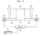
- FIG. 6is a diagram illustrating the aligning apparatus in accordance with this exemplary embodiment.
- the aligning apparatusin accordance with this exemplary embodiment includes a loading plate 310 on which an alignment object 320 is loaded, first and second alignment bars 330 and 340 for aligning the alignment object 320 loaded on the loading plate 310 , first and second motors 353 and 363 for driving the first and second alignment bars 330 and 340 in close and open directions toward and away from each other through first and second guide shafts 352 and 362 , and a control unit 390 for measuring load of the first and second motors 353 and 363 .
- the control unit 390stops driving of the first and second alignment bars 330 and 340 in the close direction toward each other and then drives the first and second alignment bars 330 and 340 in the open direction away from each other by controlling the first and second motors 353 and 363 .
- the control unit 390controls driving of the first and second motors 353 and 363 , so that the first and second alignment bars 330 and 340 can be driven in the close and open directions toward and away from each other through the first and second guide shafts 352 and 362 , for transferring and aligning the alignment object 320 loaded on the loading plate 310 in a target position.
- one motormay be installed to drive the first and second alignment bars 330 and 340 in the close and open directions through the first and second guide shafts 352 and 362 .
- This one motorsimultaneously drives the first and second alignment bars 330 and 340 in the close and open directions to and from each other through the first and second guide shafts 352 and 362 .
- a driving distance of the first and second alignment bars 330 and 340 driven in the close and open directions by the first and second motors 353 and 363is preset according to a size of the alignment object 320 .
- the load of the first and second motors 353 and 363is measured by the control unit 390 .
- the control unit 390stops driving the first and second alignment bars 330 and 340 in the close direction to each other and then drives the first and second alignment bars 330 and 340 in the open direction from each other by reversing the first and second motors 353 and 363 , thereby preventing damage to the abnormally-loaded alignment object 320 or the first and second alignment bars 330 and 340 .
- the operation of the production linecan also be stopped.
- the control unit 390measures the load of the first and second motors 353 and 363 .
- the control unit 390stops driving the first and second alignment bars 330 and 340 in the close direction toward each other and then drives the first and second alignment bars 330 and 340 in the open direction away from each other by controlling the first and second motors 353 and 363 , thereby preventing damages to the abnormally-loaded alignment object 320 or the first and second alignment bars 330 and 340 .
- the operation of the production linecan also be stopped.
- the aligning apparatusfurther includes an alarm generating unit 333 for receiving a control signal from the control unit 390 and generating an alarm, when the load of the first and second motors 353 and 363 is greater than the threshold value.
- the alarm generating unit 333When the alignment object 320 is abnormally loaded or the defective object having a larger size than the normal alignment object 320 is loaded, the alarm generating unit 333 generates the alarm and the operators can promptly resolve any errors.
- the aligning apparatuses in accordance with the exemplary embodiments of the present inventionmay be applied to an automation factory manufacturing various products according to automated processes. For example, when a fragile substrate used for fabrication of a flat panel display device is automatically transferred and aligned by an automated system such as a conveyor belt and a robot, and various processes are performed thereon, even if the substrate is abnormally loaded or a defective object having a larger size than the normal substrate is loaded, the substrate or the alignment bars are not damaged.
- FIG. 7is an exemplary diagram illustrating application of the aligning apparatus of the exemplary embodiment of the present invention to production of the substrate for a flat panel display device.
- the aligning apparatusincludes a loading plate 410 on which a substrate 420 is loaded, first and second support pins 411 A and 411 B protruded from the surface of the loading plate 410 for supporting the substrate 420 , first and second alignment bars 430 and 440 for aligning the substrate 420 supported by the first and second support pins 411 A and 411 B, first and second driving units 450 and 460 for driving the first and second alignment bars 430 and 440 in close and open directions that are toward and away from each other, and first and second elastic units 470 and 480 disposed between the first and second alignment bars 430 and 440 and the first and second driving units 450 and 460 , and bent when the first and second alignment bars 430 and 440 receive a force greater than a threshold value.
- the substrate 420may be applied to fabrication of the flat panel display device such as an electro-luminescence display (ELD), a plasma display panel (PDP), a field emission display (FED), a liquid crystal display (LCD
- the LCD devicedisplays images by controlling light transmittance of pixels arranged in a matrix shape by supplying data signals based on image information to the pixels, respectively.
- the LCDusually includes an LCD panel on which pixels are arranged in a matrix shape, and a driving circuit for driving the pixels.
- the LCD panelincludes a thin film transistor array substrate and a color filter substrate attached to face each other with a regular cell-gap, and a liquid crystal material formed in the gap between the color filter substrate and the thin film transistor array substrate.
- the thin film transistor array substrate and the color filter substrateare attached by seal patterns formed along edges of an image display unit.
- a spacermay be formed on the thin film transistor array substrate or the color filter substrate for maintaining the cell-gap between the attached thin film transistor array substrate and color filter substrate.
- a polarizing plate and a phase shift plateare disposed on the outer surfaces of the thin film transistor array substrate and the color filter substrate.
- the LCDis provided with high luminance and contrast properties by changing light proceeding or refraction by selectively using the aforementioned components. Common electrodes and pixel electrodes are formed on the LCD panel formed on the thin film transistor array substrate and the color filter substrate to face each other, for applying an electric field to the liquid crystal material.
- a plurality of LCD panelsare formed simultaneously by forming a plurality of thin film transistor array substrates on a first large-sized mother board, forming a plurality of color filter substrates on a second large-sized mother board, and soldering, cutting and processing the first and second mother boards, which results in a high yield.
- the first mother board on which the plurality of thin film transistor array substrates have been formed, the second mother board on which the plurality of color filter substrates have been formed, the attached first and second mother boards, or the LCD panel cut and processed from the attached first and second mother boardsmay be used as the substrate 420 supported by the first and second support pins 411 A and 411 B.
- three, four or more support pinsmay be installed to stably support the substrate 420 .
- the first and second alignment bars 430 and 440are driven in the close and open directions by the first and second driving units 450 and 460 , for transferring and aligning the substrate 420 supported by the first and second support pins 411 A and 411 B in a target position.
- the first and second alignment bars 430 and 440may be driven in the close and open directions by the first and second driving units 450 and 460 , for transferring and aligning the substrate 420 loaded on the loading plate 410 in a target position.
- a driving distance of the first and second alignment bars 430 and 440 driven in the close and open directions by the first and second driving units 450 and 460is preset according to a size of the substrate 420 .
- the first and second driving units 450 and 460include first and second support members 451 and 461 coupled to the first and second alignment bars 430 and 440 through the first and second elastic units 470 and 480 , and first and second motors 453 and 463 for driving the first and second support members 451 and 461 in close and open directions through first and second guide shafts 452 and 462 .
- first and second motors 453 and 463 of FIG. 7one motor may be installed to drive the first and second support members 451 and 461 in the close and open directions through the first and second guide shafts 452 and 462 . This one motor simultaneously drives the first and second support members 451 and 461 in the close and open directions through the first and second guide shafts 452 and 462 .
- the first and second elastic units 470 and 480are disposed between the first and second support members 451 and 461 of the first and second driving units 450 and 460 and the first and second alignment bars 430 and 440 , and bent by a force greater than a threshold value when the first and second alignment bars 430 and 440 are driven in the close direction to each other.
- one elastic unitmay be installed between the first support member 451 of the first driving unit 450 and the first alignment bar 430 or between the second support member 461 of the second driving unit 460 and the second alignment bar 440 . This one elastic unit is bent by a force greater than a threshold value when the first and second alignment bars 430 and 440 are driven in the close direction to each other.
- the aligning apparatus of the first embodimentwhen the aligning apparatus of the first embodiment is applied to fabrication of the flat panel display device, if the substrate 420 is abnormally loaded, that is, for example, a size of the abnormally-loaded substrate 420 is greater than an isolation distance when the first and second alignment bars 430 and 440 are driven by the first and second driving units 450 and 460 to be closest to each other, the first and second elastic units 470 and 480 disposed between the first and second driving units 450 and 460 and the first and second alignment bars 430 and 440 are bent to buffer a collision of the abnormally-loaded substrate 420 with the first and second alignment bars 430 and 440 . As a result, the substrate 420 and/or the first and second alignment bars 430 and 440 are not damaged.
- the first and second elastic units 470 and 480 disposed between the first and second driving units 450 and 460 and the first and second alignment bars 430 and 440are bent for buffering a collision of the defective object with the first and second alignment bars 430 and 440 .
- the defective object and/or the first and second alignment bars 430 and 440are not damaged.
- the LCD panel cut and processed from the attached first and second mother boards of the LCDmay be one example of the defective object having a larger size than the normal substrate 420 .
- Burrsmay remain due to defective cutting on the cross sections of the LCD panel.
- the LCD panel having the burrs on its cross sectionsmay be larger than the normal LCD panel.
- the aligning apparatusfurther includes first and second contact-type sensors 431 and 441 disposed on the sidewalls of the first and second alignment bars 430 and 440 , and a control unit 490 .
- the first and second contact-type sensors 431 and 441contact when the first and second alignment bars 430 and 440 are inclined by the bent first and second elastic units 470 and 480 .
- the control unit 490is additionally installed to stop driving the first and second alignment bars 430 and 440 in the close direction to each other and to drive the first and second alignment bars 430 and 440 in the distant direction from each other by controlling the first and second driving units 450 and 460 , when the first and second contact-type sensors 431 and 441 contact.
- the control unit 490stops driving the first and second alignment bars 430 and 440 in the close direction to each other and then drives the first and second alignment bars 430 and 440 in the distant direction from each other, by controlling the first and second driving units 450 and 460 . Therefore, when the substrate 420 is abnormally loaded or the defective object having a larger size than the normal substrate 420 is loaded, the abnormally-loaded substrate 420 , the defective object, and/or the first and second alignment bars 430 and 440 are not damaged, and an operation of a production line can be safely stopped.
- the aligning apparatusfurther includes first and second alarm generating units 433 and 443 installed to generate an alarm when the first and second contact-type sensors 431 and 441 contact.
- the first and second alarm generating units 433 and 443are connected directly to the first and second contact-type sensors 431 and 441 to generate the alarm when the first and second contact-type sensors 431 and 441 contact, or connected to the control unit 490 to generate the alarm according to the signal from the control unit 490 . Accordingly, when the substrate 420 is abnormally loaded or the defective object having a larger size than the normal substrate 420 is loaded, if the first and second alarm generating units 433 and 443 generate the alarm, the operators can promptly take necessary actions.
- the various examples shown in FIGS. 5A through 5Dmay be used as the first and second elastic units 470 and 480 .
- the elastic unitsare bent to incline the alignment bars, thereby preventing damage to the abnormally-loaded alignment object, the defective object, and the first and second alignment bars.
- the alarmis generated to notify any error to the operators
- the load of the motors driving the alignment barsis measured.
- the alignment barsare stopped and driven to the initial positions, thereby preventing damages to the abnormally-loaded alignment object, the defective object, and/or the first and second alignment bars.
- the alarmis generated to notify any error to the operators.
- productivityis improved by omitting the process for removing damaged pieces and the process for separating the damaged alignment bars from the aligning apparatus and coupling new alignment bars, which are performed when the alignment object or the alignment bars are damaged. Furthermore, it is possible to decrease the maintenance and repair costs for the aligning apparatus due to damage and replacement of the components
Landscapes
- Physics & Mathematics (AREA)
- Nonlinear Science (AREA)
- Chemical & Material Sciences (AREA)
- Crystallography & Structural Chemistry (AREA)
- General Physics & Mathematics (AREA)
- Optics & Photonics (AREA)
- Mathematical Physics (AREA)
- Container, Conveyance, Adherence, Positioning, Of Wafer (AREA)
- Liquid Crystal (AREA)
Abstract
Description
- The present invention claims the benefit of Korean Patent Application No. 2003-89853 filed in Korea on Dec. 10, 2003, which is hereby incorporated by reference.
- 1. Field of the Invention
- The present invention relates to an aligning apparatus, and more particularly, to an aligning apparatus for aligning an alignment object to the aligning apparatus.
- 2. Discussion of the Related Art
- In general, a factory for fabricating display devices utilizes automatic individual processes to attain mass production, improve workability, and cut down production expenses. The automatic processes automatically transfer and align products by employing an automated system, such as a conveyor belt and a robot, to perform the corresponding processes and load the process-completed products, thereby minimizing manual operations. As a result, products can be mass-produced by a small number of monitoring workers.
- An aligning apparatus for aligning a product in a target position is required to fabricate products according to the automated processes. A related art aligning apparatus will now be explained with reference to
FIGS. 1 and 2 .FIG. 1 is a diagram illustrating the related art aligning apparatus.FIG. 2 is a diagram illustrating an alignment object, a first alignment bar and a second alignment bar are damaged due to collision of the alignment object with the first and second alignment bars, when the alignment object is abnormally loaded. - Referring to
FIG. 1 , the related art aligning apparatus includes aloading plate 10 on which analignment object 20 is loaded, and first andsecond alignment bars alignment object 20 loaded on theloading plate 10. Herein, the first andsecond alignment bars alignment object 20 loaded on theloading plate 10 to a target position. As illustrated inFIG. 2 , in the related art aligning apparatus, the driving distance of the first andsecond alignment bars alignment object 20. In the event that thealignment object 20 is abnormally loaded on theloading plate 10, that is, for example, a size S1 of the abnormally-loadedalignment object 20 is greater than an isolation distance D1 when the first andsecond alignment bars alignment object 20 or the first andsecond alignment bars alignment object 20 with the first andsecond alignment bars normal alignment object 20 is loaded, the defective object or the first andsecond alignment bars second alignment bars - As described above, in the related art aligning apparatus, when the abnormally-loaded
alignment object 20 or the defective object is damaged, the operators must stop an operation of a production line and remove damaged pieces, which results in low productivity. Moreover, when the first andsecond alignment bars second alignment bars - Accordingly, the present invention is directed to an aligning apparatus that substantially obviates one or more of the problems due to limitations an disadvantages of the related art.
- An object of the present invention is to provide an aligning apparatus to prevent damage to an alignment object and the apparatus itself, when the alignment object is abnormally loaded to the aligning apparatus or a defective object is loaded onto the aligning apparatus.
- Another object of the present invention is to provide an aligning apparatus to prevent damage to a liquid crystal display panel and the apparatus itself, when the liquid crystal display panel is abnormally loaded or a defective object is loaded.
- Additional features and advantages of the invention will be set forth in the description which follows, and in part will be apparent from the description, or may be learned by practice of the invention. The objectives and other advantages of the invention will be realized and attained by the structure particularly pointed out in the written description and claims hereof as well as the appended drawings.
- To achieve these and other advantages and in accordance with the purpose of the present invention, as embodied and broadly described, the aligning apparatus includes a loading plate to load at least one alignment object, first and second alignment bars to align the at least one alignment object loaded on the loading plate, wherein the first and second alignment bars are bent by a force greater than a threshold value when contacting the alignment object, and at least one driving unit to drive the first and second alignment bars in close and open directions toward and away from each other.
- In another aspect, the aligning apparatus includes a loading plate to load at least one alignment object, first and second alignment bars to align the at least one alignment object on the loading plate, at least one driving unit to drive the first and second alignment bars in close and open directions toward and away from each other, and an elastic unit coupled to at least one of the first and second alignment bars, wherein the elastic unit is bent by a force greater than a threshold value when the first and second alignment bars contact the at least one alignment object.
- In another aspect, the aligning apparatus includes a loading plate to load at least one alignment object, first and second alignment bars to align the alignment object loaded on the loading plate, at least one motor to drive the first and second alignment bars in close and open directions toward and away from each other, and a control unit to control the at least one motor so that the first and second alignment bars is able to be transferred in target directions.
- It is to be understood that both the foregoing general description and the following detailed description are exemplary and explanatory and are intended to provide further explanation of the invention as claimed.
- The accompanying drawings, which are included to provide a further understanding of the invention and are incorporated in and constitute a part of this specification, illustrate embodiments of the invention and together with the description serve to explain the principles of the invention. In the drawings:
FIG. 1 is a diagram illustrating a related art aligning apparatus;FIG. 2 is a diagram illustrating the related art aligning apparatus ofFIG. 1 , wherein an alignment object, a first alignment bar and a second alignment bar are damaged due to collision of the alignment object with the first and second alignment bars, when the alignment object is abnormally loaded;FIG. 3 is a diagram illustrating an aligning apparatus in accordance with an exemplary embodiment of the present invention;FIG. 4 is a diagram illustrating the aligning apparatus ofFIG. 3 , wherein an alignment object and first and second alignment bars are protected by buffering a collision of the alignment object and the first and second alignment bars, when the alignment object is abnormally loaded;FIGS. 5 ato5dare exemplary diagrams illustrating various examples of first and second elastic units of the aligning apparatus ofFIG. 3 ;FIG. 6 is an exemplary diagram illustrating an aligning apparatus in accordance with another exemplary embodiment of the present invention; andFIG. 7 is an exemplary diagram illustrating application of the aligning apparatus ofFIG. 3 to fabrication of a substrate for a flat panel display device.- Reference will now be made in detail to the preferred embodiments of the present invention, examples of which are illustrated in the accompanying drawings.
FIG. 3 is a diagram illustrating an aligning apparatus in accordance with an exemplary embodiment of the present invention.FIG. 4 is a diagram illustrating the aligning apparatus ofFIG. 3 , wherein an alignment object and first and second alignment bars are protected by buffering a collision of the alignment object with the first and second alignment bars, when the alignment object is abnormally loaded.- Referring to
FIG. 3 , the aligning apparatus of this exemplary embodiment includes aloading plate 110 on which analignment object 120 is loaded, first andsecond alignment bars alignment object 120 loaded on theloading plate 110, first andsecond driving units second alignment bars elastic units second alignment bars second driving units second alignment bars - In accordance with this exemplary embodiment, the first and
second alignment bars second driving units alignment object 120 loaded on theloading plate 110 at a target position. A driving distance of the first andsecond alignment bars alignment object 120. On the other hand, the first andsecond driving units second support members second alignment bars elastic units second motors second support members second guide shafts - As an alternative to the first and
second motors second support members second guide shafts second support members second guide shafts - The first and second
elastic units second support members second alignment bars second alignment bars elastic units first support member 151 and thefirst alignment bar 130 or between thesecond support member 161 and thesecond alignment bar 140. When the first andsecond alignment bars - In accordance with the exemplary embodiment of the present invention, as shown in
FIG. 4 , in the event that thealignment object 120 is abnormally loaded, that is, for example, a size S11 of the abnormally-loadedalignment object 120 is greater than an isolation distance D1 when the first andsecond alignment bars second driving units elastic units second driving units second alignment bars alignment object 120 with the first andsecond alignment bars alignment object 120 and the first andsecond alignment bars - Similarly, when a defective object having a larger size than the
normal alignment object 120 is loaded, the first and secondelastic units second driving units second alignment bars second alignment bars second alignment bars - Referring back to
FIG. 3 , the aligning apparatus of this exemplary embodiment further includes first and second contact-type sensors second alignment bars control unit 190. The first and second contact-type sensors second alignment bars elastic units control unit 190 stops driving of the first andsecond alignment bars second alignment bars second driving units type sensors type sensors first alignment bar 130 or thesecond alignment bar 140 to make contact when the first andsecond alignment bars elastic units - As described above, when the first and second contact-
type sensors control unit 190 stops driving the first andsecond alignment bars second alignment bars second driving units alignment object 120 is abnormally loaded or the defective object having a larger size than thenormal alignment object 120 is loaded, the abnormally-loadedalignment object 120, the defective object, and the first andsecond alignment bars - In addition, the aligning apparatus of this exemplary embodiment further includes first and second
alarm generating units type sensors alarm generating units type sensors type sensors control unit 190 to generate the alarm according to the signal from thecontrol unit 190. Accordingly, when thealignment object 120 is abnormally loaded or the defective object having a larger size than thenormal alignment object 120 is loaded, once the first and secondalarm generating units - The preferred examples of the elastic units in the aligning apparatus in accordance with the present invention will now be explained with reference to
FIGS. 5A to5D.FIGS. 5A to5D are exemplary diagrams illustrating various examples of the first and secondelastic units FIG. 5A , a first example of the elastic unit includes asupport member 251 and analignment bar 230 coupled by anelastomer 270A. When thesupport member 251 is driven in one side direction, thealignment bar 230 coupled to thesupport member 251 by theelastomer 270A transfers an alignment object (120 inFIG. 4 ) in one side direction. When a force of transferring the alignment object is applied to thealignment bar 230, theelastomer 270A is not bent. However, when the alignment object is abnormally loaded or the defective object having a larger size than the normal alignment object is loaded, a force over a threshold value is applied to thealignment bar 230 to bend theelastomer 270A in the opposite direction to the driving direction of thesupport member 251, thereby preventing damages to the alignment object and thealignment bar 230. - As illustrated in
FIG. 5B , a second example of the elastic unit includes asupport member 251 and analignment bar 230 coupled by aspring 270B. In this arrangement, when thesupport member 251 is driven in one side direction, thealignment bar 230 coupled to thesupport member 251 by thespring 270B transfers the alignment object (120 inFIG. 4 ) in one side direction. When a force of transferring the alignment object is applied to thealignment bar 230, thespring 270B is not bent. However, when the alignment object is abnormally loaded or the defective object having a larger size than the normal alignment object is loaded, a force over a threshold value is applied to thealignment bar 230 to bend thespring 270B in the opposite direction to the driving direction of thesupport member 251, thereby preventing damage to the alignment object or thealignment bar 230. - Referring to
FIG. 5C , in a third example of the elastic unit, an end of ahorizontal shaft 251B of asupport member 251 formed in a reverse “L” shape is coupled to analignment bar 230 by aconnection pin 231, and a vertical shaft251A of thesupport member 251 is coupled to a lower portion of thealignment bar 230 by aspring 270C. When thesupport member 251 is driven in one side direction, thealignment bar 230 coupled to thesupport member 251 by theconnection pin 231 and thespring 270C transfers the alignment object (120 inFIG. 4 ) in one side direction. When a force of transferring the alignment object is applied to thealignment bar 230, thespring 270C supports thevertical shaft 251A of thesupport member 251 and the lower portion of thealignment bar 230 so that they are not separated. However, when the alignment object is abnormally loaded or the defective object having a larger size than the normal alignment object is loaded, a force over a threshold value is applied to thealignment bar 230 to extend thespring 270C so that an upper portion of thealignment bar 230 can be inclined in the opposite direction to the driving direction of thesupport member 251, thereby preventing damage to the alignment object or thealignment bar 230. - As illustrated in
FIG. 5D , in a fourth example of the elastic unit, an end of ahorizontal shaft 251B of asupport member 251 formed in a ‘T’ shape is coupled to analignment bar 230 by aconnection pin 231, and avertical shaft 251A of thesupport member 251 is coupled to an upper portion of thealignment bar 230 by aspring 270D. When thesupport member 251 is driven in one side direction, thealignment bar 230 coupled to thesupport member 251 by theconnection pin 231 and thespring 270D transfers the alignment object (120 inFIG. 4 ) in one side direction. When a force of transferring the alignment object is applied to thealignment bar 230, thespring 270D supports thevertical shaft 251A and the upper portion of thealignment bar 230 so that they do not approach each other. However, when the alignment object is abnormally loaded or a defective object having a larger size than the normal alignment object is loaded, a force over a threshold value is applied to thealignment bar 230 to contract thespring 270D so that the upper portion of thealignment bar 230 can incline in the opposite direction to the driving direction of thesupport member 251, thereby preventing damage to the alignment object or thealignment bar 230. - An aligning apparatus in accordance with another exemplary embodiment of the present invention will now be described with reference to
FIG. 6 .FIG. 6 is a diagram illustrating the aligning apparatus in accordance with this exemplary embodiment. - As illustrated in
FIG. 6 , the aligning apparatus in accordance with this exemplary embodiment includes aloading plate 310 on which analignment object 320 is loaded, first and second alignment bars330 and340 for aligning thealignment object 320 loaded on theloading plate 310, first andsecond motors second guide shafts control unit 390 for measuring load of the first andsecond motors control unit 390 stops driving of the first and second alignment bars330 and340 in the close direction toward each other and then drives the first and second alignment bars330 and340 in the open direction away from each other by controlling the first andsecond motors - In accordance with this exemplary embodiment, the
control unit 390 controls driving of the first andsecond motors second guide shafts alignment object 320 loaded on theloading plate 310 in a target position. As an alternative to the first andsecond motors FIG. 6 , one motor may be installed to drive the first and second alignment bars330 and340 in the close and open directions through the first andsecond guide shafts second guide shafts second motors alignment object 320. - In accordance with this exemplary embodiment, in the event that the
alignment object 320 is abnormally loaded, that is, for example, a size of the abnormally-loadedalignment object 320 is greater than an isolation distance when the first and second alignment bars330 and340 are driven by the first andsecond motors second motors control unit 390. When the load is greater than a threshold value, thecontrol unit 390 stops driving the first and second alignment bars330 and340 in the close direction to each other and then drives the first and second alignment bars330 and340 in the open direction from each other by reversing the first andsecond motors alignment object 320 or the first and second alignment bars330 and340. The operation of the production line can also be stopped. - Similarly, when a defective object having a larger size than the
normal alignment object 320 is loaded, the load of the first andsecond motors control unit 390 measures the load of the first andsecond motors control unit 390 stops driving the first and second alignment bars330 and340 in the close direction toward each other and then drives the first and second alignment bars330 and340 in the open direction away from each other by controlling the first andsecond motors alignment object 320 or the first and second alignment bars330 and340. The operation of the production line can also be stopped. - Referring back to
FIG. 6 , the aligning apparatus further includes analarm generating unit 333 for receiving a control signal from thecontrol unit 390 and generating an alarm, when the load of the first andsecond motors alignment object 320 is abnormally loaded or the defective object having a larger size than thenormal alignment object 320 is loaded, thealarm generating unit 333 generates the alarm and the operators can promptly resolve any errors. - The aligning apparatuses in accordance with the exemplary embodiments of the present invention may be applied to an automation factory manufacturing various products according to automated processes. For example, when a fragile substrate used for fabrication of a flat panel display device is automatically transferred and aligned by an automated system such as a conveyor belt and a robot, and various processes are performed thereon, even if the substrate is abnormally loaded or a defective object having a larger size than the normal substrate is loaded, the substrate or the alignment bars are not damaged.
FIG. 7 is an exemplary diagram illustrating application of the aligning apparatus of the exemplary embodiment of the present invention to production of the substrate for a flat panel display device.- Referring to
FIG. 7 , the aligning apparatus includes aloading plate 410 on which asubstrate 420 is loaded, first and second support pins411A and411B protruded from the surface of theloading plate 410 for supporting thesubstrate 420, first and second alignment bars430 and440 for aligning thesubstrate 420 supported by the first and second support pins411A and411B, first andsecond driving units elastic units second driving units substrate 420 may be applied to fabrication of the flat panel display device such as an electro-luminescence display (ELD), a plasma display panel (PDP), a field emission display (FED), a liquid crystal display (LCD), or the like. - The LCD device displays images by controlling light transmittance of pixels arranged in a matrix shape by supplying data signals based on image information to the pixels, respectively. The LCD usually includes an LCD panel on which pixels are arranged in a matrix shape, and a driving circuit for driving the pixels. The LCD panel includes a thin film transistor array substrate and a color filter substrate attached to face each other with a regular cell-gap, and a liquid crystal material formed in the gap between the color filter substrate and the thin film transistor array substrate.
- The thin film transistor array substrate and the color filter substrate are attached by seal patterns formed along edges of an image display unit. Herein, a spacer may be formed on the thin film transistor array substrate or the color filter substrate for maintaining the cell-gap between the attached thin film transistor array substrate and color filter substrate. A polarizing plate and a phase shift plate are disposed on the outer surfaces of the thin film transistor array substrate and the color filter substrate. The LCD is provided with high luminance and contrast properties by changing light proceeding or refraction by selectively using the aforementioned components. Common electrodes and pixel electrodes are formed on the LCD panel formed on the thin film transistor array substrate and the color filter substrate to face each other, for applying an electric field to the liquid crystal material. That is, in a state where a controlled voltage is applied across the common electrodes and individual pixel electrodes light transmittance of the unit pixels can be individually adjusted. In order to control the voltage applied to the pixel electrodes in each unit pixel, thin film transistors serving as switching elements are formed on the unit pixels, respectively. Oriented films are formed on the facing surfaces of the thin film transistor array substrate and the color filter substrate and rubbed, so that liquid crystals of the liquid crystal layer can be arranged in a predetermined direction.
- In the fabrication of the LCD devices, a plurality of LCD panels are formed simultaneously by forming a plurality of thin film transistor array substrates on a first large-sized mother board, forming a plurality of color filter substrates on a second large-sized mother board, and soldering, cutting and processing the first and second mother boards, which results in a high yield.
- When the aligning apparatus of the exemplary embodiment is applied to fabrication of the substrate of the LCD, the first mother board on which the plurality of thin film transistor array substrates have been formed, the second mother board on which the plurality of color filter substrates have been formed, the attached first and second mother boards, or the LCD panel cut and processed from the attached first and second mother boards may be used as the
substrate 420 supported by the first and second support pins411A and411B. Herein, three, four or more support pins may be installed to stably support thesubstrate 420. - As described above, when the aligning apparatus of the exemplary embodiment is applied to fabrication of the substrate of the flat panel display device, the first and second alignment bars430 and440 are driven in the close and open directions by the first and
second driving units substrate 420 supported by the first and second support pins411A and411B in a target position. On the other hand, after the first and second support pins411A and411B supporting thesubstrate 420 are lowered to load thesubstrate 420 on theloading plate 410, the first and second alignment bars430 and440 may be driven in the close and open directions by the first andsecond driving units substrate 420 loaded on theloading plate 410 in a target position. A driving distance of the first and second alignment bars430 and440 driven in the close and open directions by the first andsecond driving units substrate 420. - The first and
second driving units second support members elastic units second motors second support members second guide shafts second motors FIG. 7 , one motor may be installed to drive the first andsecond support members second guide shafts second support members second guide shafts - The first and second
elastic units second support members second driving units elastic units FIG. 7 , one elastic unit may be installed between thefirst support member 451 of thefirst driving unit 450 and thefirst alignment bar 430 or between thesecond support member 461 of thesecond driving unit 460 and thesecond alignment bar 440. This one elastic unit is bent by a force greater than a threshold value when the first and second alignment bars430 and440 are driven in the close direction to each other. - Accordingly, when the aligning apparatus of the first embodiment is applied to fabrication of the flat panel display device, if the
substrate 420 is abnormally loaded, that is, for example, a size of the abnormally-loadedsubstrate 420 is greater than an isolation distance when the first and second alignment bars430 and440 are driven by the first andsecond driving units elastic units second driving units substrate 420 with the first and second alignment bars430 and440. As a result, thesubstrate 420 and/or the first and second alignment bars430 and440 are not damaged. - Similarly, when a defective object having a larger size than the
normal substrate 420 is loaded, the first and secondelastic units second driving units - Herein, the LCD panel cut and processed from the attached first and second mother boards of the LCD may be one example of the defective object having a larger size than the
normal substrate 420. Burrs may remain due to defective cutting on the cross sections of the LCD panel. The LCD panel having the burrs on its cross sections may be larger than the normal LCD panel. When LCD panel is aligned by the first and second alignment bars430 and440, the first and second alignment bars430 and440 receive a greater force than the threshold value, and thus the first and secondelastic units FIG. 7 , the aligning apparatus further includes first and second contact-type sensors control unit 490. The first and second contact-type sensors elastic units control unit 490 is additionally installed to stop driving the first and second alignment bars430 and440 in the close direction to each other and to drive the first and second alignment bars430 and440 in the distant direction from each other by controlling the first andsecond driving units type sensors - As described above, when the first and second contact-
type sensors control unit 490 stops driving the first and second alignment bars430 and440 in the close direction to each other and then drives the first and second alignment bars430 and440 in the distant direction from each other, by controlling the first andsecond driving units substrate 420 is abnormally loaded or the defective object having a larger size than thenormal substrate 420 is loaded, the abnormally-loadedsubstrate 420, the defective object, and/or the first and second alignment bars430 and440 are not damaged, and an operation of a production line can be safely stopped. - In addition, the aligning apparatus further includes first and second
alarm generating units type sensors alarm generating units type sensors type sensors control unit 490 to generate the alarm according to the signal from thecontrol unit 490. Accordingly, when thesubstrate 420 is abnormally loaded or the defective object having a larger size than thenormal substrate 420 is loaded, if the first and secondalarm generating units FIGS. 5A through 5D may be used as the first and secondelastic units - Since application of the aligning apparatus of the exemplary embodiment to fabrication of the substrate of the flat panel display device has been described in detail with reference to
FIG. 7 , although not explained, application of the aligning apparatus of the other exemplary embodiment to fabrication of the substrate of the flat panel display device is easily understood by those skilled in the art to which the present invention pertains. - As discussed earlier, in accordance with the exemplary embodiment of the present invention, when the alignment object is abnormally loaded or the defective object having a larger size than the normal alignment object is loaded, the elastic units are bent to incline the alignment bars, thereby preventing damage to the abnormally-loaded alignment object, the defective object, and the first and second alignment bars. In addition, the alarm is generated to notify any error to the operators
- In accordance with the other exemplary embodiment of the present invention, the load of the motors driving the alignment bars is measured. When the alignment object is abnormally loaded or the defective object having a larger size than the normal alignment object is loaded and the load of the motors is greater than the threshold value, the alignment bars are stopped and driven to the initial positions, thereby preventing damages to the abnormally-loaded alignment object, the defective object, and/or the first and second alignment bars. Also, the alarm is generated to notify any error to the operators.
- As a result, in accordance with the exemplary embodiments of the present invention, productivity is improved by omitting the process for removing damaged pieces and the process for separating the damaged alignment bars from the aligning apparatus and coupling new alignment bars, which are performed when the alignment object or the alignment bars are damaged. Furthermore, it is possible to decrease the maintenance and repair costs for the aligning apparatus due to damage and replacement of the components
- It will be apparent to those skilled in the art that various modifications and variations can be made in the aligning apparatus of the present invention without departing from the spirit or scope of the invention. Thus, it is intended that the present invention cover the modifications and variations of this invention provided they come within the scope of the appended claims and their equivalents.
Claims (38)
Priority Applications (1)
| Application Number | Priority Date | Filing Date | Title |
|---|---|---|---|
| US11/808,747US7377049B2 (en) | 2003-12-10 | 2007-06-12 | Aligning apparatus |
Applications Claiming Priority (3)
| Application Number | Priority Date | Filing Date | Title |
|---|---|---|---|
| KRP2003-89853 | 2003-12-10 | ||
| KR10-2003-0089853 | 2003-12-10 | ||
| KR1020030089853AKR101003666B1 (en) | 2003-12-10 | 2003-12-10 | Aligner |
Related Child Applications (1)
| Application Number | Title | Priority Date | Filing Date |
|---|---|---|---|
| US11/808,747DivisionUS7377049B2 (en) | 2003-12-10 | 2007-06-12 | Aligning apparatus |
Publications (2)
| Publication Number | Publication Date |
|---|---|
| US20050126028A1true US20050126028A1 (en) | 2005-06-16 |
| US7240438B2 US7240438B2 (en) | 2007-07-10 |
Family
ID=34651358
Family Applications (2)
| Application Number | Title | Priority Date | Filing Date |
|---|---|---|---|
| US11/008,272Expired - Fee RelatedUS7240438B2 (en) | 2003-12-10 | 2004-12-10 | Aligning apparatus |
| US11/808,747Expired - LifetimeUS7377049B2 (en) | 2003-12-10 | 2007-06-12 | Aligning apparatus |
Family Applications After (1)
| Application Number | Title | Priority Date | Filing Date |
|---|---|---|---|
| US11/808,747Expired - LifetimeUS7377049B2 (en) | 2003-12-10 | 2007-06-12 | Aligning apparatus |
Country Status (3)
| Country | Link |
|---|---|
| US (2) | US7240438B2 (en) |
| KR (1) | KR101003666B1 (en) |
| CN (1) | CN100362402C (en) |
Cited By (4)
| Publication number | Priority date | Publication date | Assignee | Title |
|---|---|---|---|---|
| US20070131733A1 (en)* | 2005-12-12 | 2007-06-14 | Asm Assembly Automation Ltd. | Apparatus and method for arranging devices for processing |
| US20080169595A1 (en)* | 2007-01-12 | 2008-07-17 | Shenzhen Futaihong Precision Industrial Co.,Ltd. | Flexible fixing system for product testing |
| US20110282484A1 (en)* | 2010-05-12 | 2011-11-17 | Tokyo Electron Limited | Substrate positioning apparatus, substrate processing apparatus, substrate positioning method, and computer readable medium having a program stored thereon |
| US20150063969A1 (en)* | 2013-09-04 | 2015-03-05 | Infineon Technologies Ag | Method and Apparatus for Dynamic Alignment of Semiconductor Devices |
Families Citing this family (13)
| Publication number | Priority date | Publication date | Assignee | Title |
|---|---|---|---|---|
| KR101003666B1 (en)* | 2003-12-10 | 2010-12-23 | 엘지디스플레이 주식회사 | Aligner |
| KR101138728B1 (en)* | 2005-08-19 | 2012-04-24 | 엘아이지에이디피 주식회사 | Substrate Alignment Apparatus and FPD Automatic Optical Inspection Using Same |
| KR100857833B1 (en)* | 2007-08-06 | 2008-09-10 | 현대자동차주식회사 | Auto body alignment device for commercial vehicle assembly and control method |
| JP5449239B2 (en)* | 2010-05-12 | 2014-03-19 | 東京エレクトロン株式会社 | Substrate processing apparatus, substrate processing method, and storage medium storing program |
| US20120032380A1 (en)* | 2010-08-09 | 2012-02-09 | Valeri Riachentsev | PCB holder |
| KR101232103B1 (en)* | 2010-09-15 | 2013-02-12 | 신은경 | Structure Support Member Apparatus |
| US9144860B2 (en)* | 2012-03-29 | 2015-09-29 | Fanuc Robotics America Corporation | Robotic weld gun orientation normalization |
| CN103852923A (en)* | 2014-03-27 | 2014-06-11 | 苏州光宝康电子有限公司 | Device for LCD (liquid crystal display) automatic alignment |
| CN103985662B (en)* | 2014-04-24 | 2017-07-04 | 京东方科技集团股份有限公司 | A kind of alignment device and to bit platform |
| CN108475051B (en)* | 2016-02-02 | 2022-01-25 | Abb瑞士股份有限公司 | Method and system for aligning a tool during programming of an industrial robot |
| CN107230657B (en)* | 2016-03-24 | 2019-07-02 | 沈阳芯源微电子设备股份有限公司 | A kind of wafer centering body |
| CN107367857B (en)* | 2017-07-13 | 2020-07-28 | 武汉华星光电技术有限公司 | Aligning device |
| CN110026757B (en)* | 2019-05-27 | 2021-02-26 | 盐城工学院 | A pull-out assembly detection system and detection method for an automatic assembly line of a fuel pump |
Citations (51)
| Publication number | Priority date | Publication date | Assignee | Title |
|---|---|---|---|---|
| US3978580A (en)* | 1973-06-28 | 1976-09-07 | Hughes Aircraft Company | Method of fabricating a liquid crystal display |
| US4094058A (en)* | 1976-07-23 | 1978-06-13 | Omron Tateisi Electronics Co. | Method of manufacture of liquid crystal displays |
| US4189230A (en)* | 1977-10-26 | 1980-02-19 | Fujitsu Limited | Wafer holder with spring-loaded wafer-holding means |
| US4425076A (en)* | 1980-12-24 | 1984-01-10 | Compagne Internationale pour l'Informatique Cii Honeywell Bull (Societe Anonyme) | Process and apparatus for automatic positioning of a substrate on a worktable |
| US4516318A (en)* | 1983-04-26 | 1985-05-14 | At&T Technologies, Inc. | Methods of processing substrates |
| US4563824A (en)* | 1983-12-12 | 1986-01-14 | Charlton Associates | Method and apparatus for disc position centering |
| US4653864A (en)* | 1986-02-26 | 1987-03-31 | Ovonic Imaging Systems, Inc. | Liquid crystal matrix display having improved spacers and method of making same |
| US4691995A (en)* | 1985-07-15 | 1987-09-08 | Semiconductor Energy Laboratory Co., Ltd. | Liquid crystal filling device |
| US4775225A (en)* | 1985-05-16 | 1988-10-04 | Canon Kabushiki Kaisha | Liquid crystal device having pillar spacers with small base periphery width in direction perpendicular to orientation treatment |
| US4860439A (en)* | 1988-10-25 | 1989-08-29 | Riley Bryan R | Universal alignment fixture |
| US5247377A (en)* | 1988-07-23 | 1993-09-21 | Rohm Gmbh Chemische Fabrik | Process for producing anisotropic liquid crystal layers on a substrate |
| US5263888A (en)* | 1992-02-20 | 1993-11-23 | Matsushita Electric Industrial Co., Ltd. | Method of manufacture of liquid crystal display panel |
| US5379139A (en)* | 1986-08-20 | 1995-01-03 | Semiconductor Energy Laboratory Co., Ltd. | Liquid crystal device and method for manufacturing same with spacers formed by photolithography |
| US5406989A (en)* | 1993-10-12 | 1995-04-18 | Ayumi Industry Co., Ltd. | Method and dispenser for filling liquid crystal into LCD cell |
| US5499128A (en)* | 1993-03-15 | 1996-03-12 | Kabushiki Kaisha Toshiba | Liquid crystal display device with acrylic polymer spacers and method of manufacturing the same |
| US5507323A (en)* | 1993-10-12 | 1996-04-16 | Fujitsu Limited | Method and dispenser for filling liquid crystal into LCD cell |
| US5539545A (en)* | 1993-05-18 | 1996-07-23 | Semiconductor Energy Laboratory Co., Ltd. | Method of making LCD in which resin columns are cured and the liquid crystal is reoriented |
| US5548429A (en)* | 1993-06-14 | 1996-08-20 | Canon Kabushiki Kaisha | Process for producing liquid crystal device whereby curing the sealant takes place after pre-baking the substrates |
| US5642214A (en)* | 1991-07-19 | 1997-06-24 | Sharp Kabushiki Kaisha | Optical modulating element and electronic apparatus using it |
| US5707052A (en)* | 1996-08-26 | 1998-01-13 | Motorola, Inc. | System for supporting a printed circuit board during assembly |
| US5742370A (en)* | 1996-09-12 | 1998-04-21 | Korea Institute Of Science And Technology | Fabrication method for liquid crystal alignment layer by magnetic field treatment |
| US5757451A (en)* | 1995-09-08 | 1998-05-26 | Kabushiki Kaisha Toshiba | Liquid crystal display device spacers formed from stacked color layers |
| US5852484A (en)* | 1994-09-26 | 1998-12-22 | Matsushita Electric Industrial Co., Ltd. | Liquid crystal display panel and method and device for manufacturing the same |
| US5861932A (en)* | 1997-03-31 | 1999-01-19 | Denso Corporation | Liquid crystal cell and its manufacturing method |
| US5875922A (en)* | 1997-10-10 | 1999-03-02 | Nordson Corporation | Apparatus for dispensing an adhesive |
| US5956112A (en)* | 1995-10-02 | 1999-09-21 | Sharp Kabushiki Kaisha | Liquid crystal display device and method for manufacturing the same |
| US5974654A (en)* | 1997-05-22 | 1999-11-02 | Matsushita Electric Industrial Co., Ltd. | Printed board positioning method |
| US6001203A (en)* | 1995-03-01 | 1999-12-14 | Matsushita Electric Industrial Co., Ltd. | Production process of liquid crystal display panel, seal material for liquid crystal cell and liquid crystal display |
| US6011609A (en)* | 1996-10-05 | 2000-01-04 | Samsung Electronics Co., Ltd. | Method of manufacturing LCD by dropping liquid crystals on a substrate and then pressing the substrates |
| US6016181A (en)* | 1996-11-07 | 2000-01-18 | Sharp Kabushiki Kaisha | Liquid crystal device having column spacers with portion on each of the spacers for reflecting or absorbing visible light and method for fabricating the same |
| US6016178A (en)* | 1996-09-13 | 2000-01-18 | Sony Corporation | Reflective guest-host liquid-crystal display device |
| US6055035A (en)* | 1998-05-11 | 2000-04-25 | International Business Machines Corporation | Method and apparatus for filling liquid crystal display (LCD) panels |
| US6163357A (en)* | 1996-09-26 | 2000-12-19 | Kabushiki Kaisha Toshiba | Liquid crystal display device having the driving circuit disposed in the seal area, with different spacer density in driving circuit area than display area |
| US6190997B1 (en)* | 1998-07-02 | 2001-02-20 | Robert Bosch Gmbh | Device for mechanically aligning a carrier substrate for electronic circuits |
| US6219126B1 (en)* | 1998-11-20 | 2001-04-17 | International Business Machines Corporation | Panel assembly for liquid crystal displays having a barrier fillet and an adhesive fillet in the periphery |
| US6226067B1 (en)* | 1997-10-03 | 2001-05-01 | Minolta Co., Ltd. | Liquid crystal device having spacers and manufacturing method thereof |
| US6236445B1 (en)* | 1996-02-22 | 2001-05-22 | Hughes Electronics Corporation | Method for making topographic projections |
| US6304311B1 (en)* | 1998-11-16 | 2001-10-16 | Matsushita Electric Industrial Co., Ltd. | Method of manufacturing liquid crystal display device |
| US6304306B1 (en)* | 1995-02-17 | 2001-10-16 | Sharp Kabushiki Kaisha | Liquid crystal display device and method for producing the same |
| US6333636B1 (en)* | 1997-12-08 | 2001-12-25 | Samsung Electronics Co., Ltd. | Semiconductor wafer aligning system and method using same |
| US6337730B1 (en)* | 1998-06-02 | 2002-01-08 | Denso Corporation | Non-uniformly-rigid barrier wall spacers used to correct problems caused by thermal contraction of smectic liquid crystal material |
| US6414733B1 (en)* | 1999-02-08 | 2002-07-02 | Dai Nippon Printing Co., Ltd. | Color liquid crystal display with a shielding member being arranged between sealing member and display zone |
| US6437296B1 (en)* | 2000-12-21 | 2002-08-20 | Lg. Philips Lcd Co. Ltd. | Alignment apparatus of the substrate for LCD |
| US6442818B1 (en)* | 2000-03-28 | 2002-09-03 | Avaya Technology Corp. | Method for positioning components having critical positioning tolerances for attachment to a circuit board |
| US6530157B1 (en)* | 2001-09-04 | 2003-03-11 | Process Integration | Precise positioning device for workpieces |
| US6680775B1 (en)* | 1998-04-02 | 2004-01-20 | Nikon Corporation | Substrate treating device and method, and exposure device and method |
| US6754971B1 (en)* | 1998-07-25 | 2004-06-29 | Fa. Oskar Braunsberger | Centering device for flat components, especially glass panels |
| US6811131B2 (en)* | 2002-02-08 | 2004-11-02 | Hannstar Display Corp. | Adjustable supporting tool for LCD panel |
| US6879370B2 (en)* | 2001-12-14 | 2005-04-12 | International Business Machines Corporation | Fixing device, method of fixing substrate and apparatus and method for manufacturing a liquid crystal display panel using the same |
| US6885437B2 (en)* | 2001-08-20 | 2005-04-26 | Nikon Corporation | Mask exchanging method and exposure apparatus |
| US7084961B2 (en)* | 2003-12-22 | 2006-08-01 | Asml Netherlands B.V. | Safety mechanism for a lithographic patterning device |
Family Cites Families (203)
| Publication number | Priority date | Publication date | Assignee | Title |
|---|---|---|---|---|
| JPS5811389B2 (en) | 1974-12-03 | 1983-03-02 | インステイチユ−ト プロブレム マテリアロヴエデニア アカデミイ ナウク ウクラインスコイ エスエスア−ル | Kenma Zaino Metalization |
| JPS5738414A (en) | 1980-08-20 | 1982-03-03 | Showa Denko Kk | Spacer for display panel |
| JPS5788428A (en) | 1980-11-20 | 1982-06-02 | Ricoh Elemex Corp | Manufacture of liquid crystal display body device |
| JPS5827126A (en) | 1981-08-11 | 1983-02-17 | Nec Corp | Production of liquid crystal display panel |
| JPS5957221A (en) | 1982-09-28 | 1984-04-02 | Asahi Glass Co Ltd | Production of display element |
| US4467250A (en)* | 1982-12-10 | 1984-08-21 | Newport Corporation | Electric motor controls for mechanical actuators |
| JPS59195222A (en) | 1983-04-19 | 1984-11-06 | Matsushita Electric Ind Co Ltd | Manufacture of liquid-crystal panel |
| JPS60111221A (en) | 1983-11-19 | 1985-06-17 | Nippon Denso Co Ltd | Method and device for charging liquid crystal |
| JPS60164723A (en) | 1984-02-07 | 1985-08-27 | Seiko Instr & Electronics Ltd | Liquid crystal display device |
| JPS60217343A (en) | 1984-04-13 | 1985-10-30 | Matsushita Electric Ind Co Ltd | Liquid crystal display device and its preparation |
| JPS617822A (en) | 1984-06-22 | 1986-01-14 | Canon Inc | Production of liquid crystal element |
| JPS6155625A (en) | 1984-08-24 | 1986-03-20 | Nippon Denso Co Ltd | Manufacture of liquid crystal element |
| JP2616761B2 (en) | 1985-07-15 | 1997-06-04 | 株式会社 半導体エネルギー研究所 | Method for manufacturing liquid crystal display device |
| JP2535142B2 (en) | 1985-07-15 | 1996-09-18 | 株式会社 半導体エネルギー研究所 | Liquid crystal display device manufacturing method |
| JPS6254228A (en) | 1985-07-15 | 1987-03-09 | Semiconductor Energy Lab Co Ltd | Manufacturing method for liquid crystal display |
| JPS6289025A (en) | 1985-10-15 | 1987-04-23 | Matsushita Electric Ind Co Ltd | Manufacturing method of liquid crystal display panel |
| JPS6290622A (en) | 1985-10-17 | 1987-04-25 | Seiko Epson Corp | liquid crystal display device |
| US4696501A (en)* | 1986-01-30 | 1987-09-29 | Honeywell Inc. | Robot gripper |
| JPH0668589B2 (en) | 1986-03-06 | 1994-08-31 | キヤノン株式会社 | Ferroelectric liquid crystal element |
| US5963288A (en) | 1987-08-20 | 1999-10-05 | Semiconductor Energy Laboratory Co., Ltd. | Liquid crystal device having sealant and spacers made from the same material |
| JPS63109413A (en) | 1986-10-27 | 1988-05-14 | Fujitsu Ltd | Manufacturing method of LCD display |
| JPS63110425A (en) | 1986-10-29 | 1988-05-14 | Toppan Printing Co Ltd | Cell for liquid crystal filling |
| JPS63128315A (en) | 1986-11-19 | 1988-05-31 | Victor Co Of Japan Ltd | Liquid crystal display element |
| JPS63311233A (en) | 1987-06-12 | 1988-12-20 | Toyota Motor Corp | lcd cell |
| JPH01177976A (en)* | 1988-01-07 | 1989-07-14 | Nec Corp | Rectangular object positioning mechanism |
| US4964078A (en) | 1989-05-16 | 1990-10-16 | Motorola, Inc. | Combined multiple memories |
| JPH0536425A (en) | 1991-02-12 | 1993-02-12 | Tokyo Electric Power Co Inc:The | Alloy separator for solid oxide fuel cell and method for producing the same |
| JP3068264B2 (en) | 1991-07-31 | 2000-07-24 | 三菱重工業株式会社 | Solid electrolyte fuel cell |
| JPH05109533A (en) | 1991-10-16 | 1993-04-30 | Hitachi Metals Ltd | Co base soft magnetic thin film and magnetic head using it |
| JPH05107533A (en) | 1991-10-16 | 1993-04-30 | Shinetsu Eng Kk | Method for laminating glass substrate for liquid crystal display panel and laminating apparatus therefor |
| JPH05127179A (en) | 1991-11-01 | 1993-05-25 | Ricoh Co Ltd | Production of liquid crystal display element |
| JPH05127719A (en) | 1991-11-01 | 1993-05-25 | Fuji Electric Co Ltd | Data loader of positioning controller |
| JP2609386B2 (en) | 1991-12-06 | 1997-05-14 | 株式会社日立製作所 | Board assembly equipment |
| JPH05265011A (en) | 1992-03-19 | 1993-10-15 | Seiko Instr Inc | Production of liquid crystal display element |
| JPH05281562A (en) | 1992-04-01 | 1993-10-29 | Matsushita Electric Ind Co Ltd | Manufacture of liquid crystal panel |
| JP2939384B2 (en) | 1992-04-01 | 1999-08-25 | 松下電器産業株式会社 | Liquid crystal panel manufacturing method |
| JP2604090B2 (en) | 1992-06-30 | 1997-04-23 | 信越エンジニアリング株式会社 | Glass substrate bonding equipment for liquid crystal display panels |
| JPH0651256A (en) | 1992-07-30 | 1994-02-25 | Matsushita Electric Ind Co Ltd | Device for discharging liquid crystal |
| JPH0664229A (en) | 1992-08-24 | 1994-03-08 | Toshiba Corp | Optical printing head |
| JP3084975B2 (en) | 1992-11-06 | 2000-09-04 | 松下電器産業株式会社 | Liquid crystal display cell manufacturing equipment |
| JPH06160871A (en) | 1992-11-26 | 1994-06-07 | Matsushita Electric Ind Co Ltd | Liquid crystal display panel and manufacturing method thereof |
| JPH06194637A (en) | 1992-12-24 | 1994-07-15 | Shinetsu Eng Kk | Method for sticking glass substrate for liquid crystal display plate |
| JPH06235925A (en) | 1993-02-10 | 1994-08-23 | Matsushita Electric Ind Co Ltd | Manufacture of liquid crystal display element |
| JPH06265915A (en) | 1993-03-12 | 1994-09-22 | Matsushita Electric Ind Co Ltd | Discharge device for filling liquid crystal |
| JP3170773B2 (en) | 1993-04-28 | 2001-05-28 | 株式会社日立製作所 | Board assembly equipment |
| JP3260511B2 (en) | 1993-09-13 | 2002-02-25 | 株式会社日立製作所 | Sealant drawing method |
| JPH07128674A (en) | 1993-11-05 | 1995-05-19 | Matsushita Electric Ind Co Ltd | Liquid crystal display element manufacturing method |
| JPH07181507A (en) | 1993-12-21 | 1995-07-21 | Canon Inc | Liquid crystal display device and information transmission device including the liquid crystal display device |
| JP2809588B2 (en) | 1994-04-06 | 1998-10-08 | 日立テクノエンジニアリング株式会社 | Paste coating machine |
| JP2880642B2 (en) | 1994-04-11 | 1999-04-12 | 日立テクノエンジニアリング株式会社 | Paste coating machine |
| JP3023282B2 (en) | 1994-09-02 | 2000-03-21 | 信越エンジニアリング株式会社 | Surface plate structure in glass substrate bonding equipment for liquid crystal display panels |
| JP3189591B2 (en) | 1994-09-27 | 2001-07-16 | 松下電器産業株式会社 | Manufacturing method of liquid crystal element |
| JPH08101395A (en) | 1994-09-30 | 1996-04-16 | Matsushita Electric Ind Co Ltd | Liquid crystal display element manufacturing method |
| JPH08106101A (en) | 1994-10-06 | 1996-04-23 | Fujitsu Ltd | Liquid crystal display panel manufacturing method |
| JP2665319B2 (en) | 1994-10-13 | 1997-10-22 | 信越エンジニアリング株式会社 | Glass substrate heating device for liquid crystal display panel |
| JP3053535B2 (en) | 1994-11-09 | 2000-06-19 | 信越エンジニアリング株式会社 | Pressurizing and heating equipment for glass substrates for liquid crystal display panels |
| JPH08171094A (en) | 1994-12-19 | 1996-07-02 | Nippon Soken Inc | Liquid crystal injecting method and liquid crystal injecting device to liquid crystal display device |
| JP3122708B2 (en) | 1994-12-26 | 2001-01-09 | 日立テクノエンジニアリング株式会社 | Paste coating machine |
| JP3545076B2 (en) | 1995-01-11 | 2004-07-21 | 富士通ディスプレイテクノロジーズ株式会社 | Liquid crystal display device and method of manufacturing the same |
| JP3534474B2 (en) | 1995-03-06 | 2004-06-07 | 富士通ディスプレイテクノロジーズ株式会社 | Liquid crystal display panel sealing method |
| JPH095762A (en) | 1995-06-20 | 1997-01-10 | Matsushita Electric Ind Co Ltd | Liquid crystal panel manufacturing method |
| JPH091026A (en) | 1995-06-23 | 1997-01-07 | Hitachi Techno Eng Co Ltd | Paste applicator |
| JP3139945B2 (en) | 1995-09-29 | 2001-03-05 | 日立テクノエンジニアリング株式会社 | Paste coating machine |
| JP3978241B2 (en) | 1995-07-10 | 2007-09-19 | シャープ株式会社 | Liquid crystal display panel and manufacturing method thereof |
| JPH0961829A (en) | 1995-08-21 | 1997-03-07 | Matsushita Electric Ind Co Ltd | Liquid crystal display element manufacturing method |
| JPH0961828A (en) | 1995-08-25 | 1997-03-07 | Canon Inc | Liquid crystal element and manufacturing method thereof |
| JPH0973075A (en) | 1995-09-05 | 1997-03-18 | Matsushita Electric Ind Co Ltd | Liquid crystal display element manufacturing method and liquid crystal display element manufacturing apparatus |
| JP3161296B2 (en) | 1995-09-05 | 2001-04-25 | 松下電器産業株式会社 | Manufacturing method of liquid crystal display element |
| JP3658604B2 (en) | 1995-10-27 | 2005-06-08 | 富士通ディスプレイテクノロジーズ株式会社 | Manufacturing method of liquid crystal panel |
| JPH09230357A (en) | 1996-02-22 | 1997-09-05 | Canon Inc | Liquid crystal panel manufacturing method and liquid crystal cell used therefor |
| JP3790295B2 (en) | 1996-04-17 | 2006-06-28 | シャープ株式会社 | Manufacturing method of liquid crystal display panel |
| JP3234496B2 (en) | 1996-05-21 | 2001-12-04 | 松下電器産業株式会社 | Manufacturing method of liquid crystal display device |
| KR200143155Y1 (en)* | 1996-06-20 | 1999-06-01 | 김영환 | Align instrument for lcd |
| JPH10123537A (en) | 1996-10-15 | 1998-05-15 | Matsushita Electric Ind Co Ltd | Liquid crystal display device and method of manufacturing the same |
| JP3088960B2 (en) | 1996-10-22 | 2000-09-18 | 松下電器産業株式会社 | Manufacturing method of liquid crystal display element |
| JPH10142616A (en) | 1996-11-14 | 1998-05-29 | Ayumi Kogyo Kk | Liquid crystal injection method and liquid dispenser |
| JP3372799B2 (en) | 1996-12-17 | 2003-02-04 | 株式会社 日立インダストリイズ | Paste coating machine |
| JPH10177178A (en) | 1996-12-17 | 1998-06-30 | Matsushita Electric Ind Co Ltd | Manufacturing method of liquid crystal display element |
| JP3874871B2 (en) | 1997-02-10 | 2007-01-31 | シャープ株式会社 | Manufacturing method of liquid crystal display device |
| JP3773326B2 (en) | 1997-04-07 | 2006-05-10 | アユミ工業株式会社 | Liquid crystal injection method and dispenser used therefor |
| JPH10333157A (en) | 1997-06-03 | 1998-12-18 | Matsushita Electric Ind Co Ltd | Manufacturing method of liquid crystal display device |
| JPH10333159A (en) | 1997-06-03 | 1998-12-18 | Matsushita Electric Ind Co Ltd | Liquid crystal display |
| JPH1114953A (en) | 1997-06-20 | 1999-01-22 | Matsushita Electric Ind Co Ltd | Method of manufacturing multi-touch liquid crystal display panel and multi-touch liquid crystal display panel |
| JP3874895B2 (en) | 1997-07-23 | 2007-01-31 | シャープ株式会社 | Manufacturing method of liquid crystal display panel |
| JPH1164811A (en) | 1997-08-21 | 1999-03-05 | Matsushita Electric Ind Co Ltd | Method and apparatus for manufacturing liquid crystal display element |
| JPH11109388A (en) | 1997-10-03 | 1999-04-23 | Hitachi Ltd | Manufacturing method of liquid crystal display device |
| JPH11133438A (en) | 1997-10-24 | 1999-05-21 | Matsushita Electric Ind Co Ltd | Liquid crystal display device and its manufacturing method |
| JPH11142864A (en) | 1997-11-07 | 1999-05-28 | Matsushita Electric Ind Co Ltd | Manufacturing method of liquid crystal display device |
| JPH11174477A (en) | 1997-12-08 | 1999-07-02 | Matsushita Electric Ind Co Ltd | Manufacturing method of liquid crystal display device |
| JPH11264991A (en) | 1998-01-13 | 1999-09-28 | Matsushita Electric Ind Co Ltd | Manufacturing method of liquid crystal display element |
| JPH11212045A (en) | 1998-01-26 | 1999-08-06 | Matsushita Electric Ind Co Ltd | Liquid crystal panel manufacturing method |
| JPH11248930A (en) | 1998-03-06 | 1999-09-17 | Matsushita Electric Ind Co Ltd | Color filter substrate, method of manufacturing the color filter substrate, and liquid crystal display device using the color filter substrate |
| JP3492190B2 (en) | 1998-03-17 | 2004-02-03 | 株式会社 日立インダストリイズ | Paste application method and paste application machine |
| JPH11326922A (en) | 1998-05-14 | 1999-11-26 | Matsushita Electric Ind Co Ltd | Liquid crystal display panel manufacturing method |
| JPH11344714A (en) | 1998-06-02 | 1999-12-14 | Denso Corp | Liquid crystal cell |
| JP3148859B2 (en) | 1998-06-12 | 2001-03-26 | 松下電器産業株式会社 | Apparatus and method for assembling liquid crystal panel |
| JP2000029035A (en) | 1998-07-09 | 2000-01-28 | Minolta Co Ltd | Liquid crystal element and its manufacture |
| JP3215086B2 (en)* | 1998-07-09 | 2001-10-02 | ファナック株式会社 | Robot controller |
| JP2000056311A (en) | 1998-08-03 | 2000-02-25 | Matsushita Electric Ind Co Ltd | Liquid crystal display |
| JP2000066165A (en) | 1998-08-20 | 2000-03-03 | Matsushita Electric Ind Co Ltd | Liquid crystal display panel manufacturing method |
| JP2934438B1 (en) | 1998-08-21 | 1999-08-16 | 信越エンジニアリング株式会社 | LCD panel manufacturing equipment |
| JP3520205B2 (en) | 1998-09-18 | 2004-04-19 | 株式会社 日立インダストリイズ | Paste application method and paste application machine |
| JP2000137235A (en) | 1998-11-02 | 2000-05-16 | Matsushita Electric Ind Co Ltd | Liquid crystal substrate bonding method |
| JP2000206538A (en)* | 1998-11-09 | 2000-07-28 | Matsushita Electric Ind Co Ltd | Method and apparatus for manufacturing liquid crystal display element and liquid crystal display element |
| KR20000035302A (en)* | 1998-11-09 | 2000-06-26 | 마츠시타 덴끼 산교 가부시키가이샤 | Manufacturing method and apparatus of liquid crystal display |
| JP2000193988A (en) | 1998-12-25 | 2000-07-14 | Fujitsu Ltd | Method and apparatus for manufacturing liquid crystal display panel |
| JP2000241824A (en) | 1999-02-18 | 2000-09-08 | Matsushita Electric Ind Co Ltd | Manufacturing method of liquid crystal display device |
| JP2000310784A (en) | 1999-02-22 | 2000-11-07 | Matsushita Electric Ind Co Ltd | Liquid crystal panel, color filter and method for producing them |
| JP3535044B2 (en) | 1999-06-18 | 2004-06-07 | 株式会社 日立インダストリイズ | Substrate assembling apparatus and method, and liquid crystal panel manufacturing method |
| JP3410983B2 (en) | 1999-03-30 | 2003-05-26 | 株式会社 日立インダストリイズ | Substrate assembly method and apparatus |
| JP2000292799A (en) | 1999-04-09 | 2000-10-20 | Matsushita Electric Ind Co Ltd | Liquid crystal display device and method of manufacturing the same |
| JP2000310759A (en) | 1999-04-28 | 2000-11-07 | Matsushita Electric Ind Co Ltd | Liquid crystal display device manufacturing apparatus and method |
| JP2001013506A (en) | 1999-04-30 | 2001-01-19 | Matsushita Electric Ind Co Ltd | Liquid crystal display device and method of manufacturing the same |
| JP2001222017A (en) | 1999-05-24 | 2001-08-17 | Fujitsu Ltd | Liquid crystal display device and method of manufacturing the same |
| JP2000338501A (en) | 1999-05-26 | 2000-12-08 | Matsushita Electric Ind Co Ltd | Liquid crystal display panel manufacturing method |
| JP3486862B2 (en) | 1999-06-21 | 2004-01-13 | 株式会社 日立インダストリイズ | Substrate assembly method and apparatus |
| JP2001033793A (en) | 1999-07-21 | 2001-02-09 | Matsushita Electric Ind Co Ltd | Liquid crystal display panel and method of manufacturing the same |
| JP3422291B2 (en) | 1999-08-03 | 2003-06-30 | 株式会社 日立インダストリイズ | How to assemble a liquid crystal substrate |
| JP2001051284A (en) | 1999-08-10 | 2001-02-23 | Matsushita Electric Ind Co Ltd | Liquid crystal display device manufacturing equipment |
| JP2001091727A (en) | 1999-09-27 | 2001-04-06 | Matsushita Electric Ind Co Ltd | Method for manufacturing color filter substrate, color filter substrate and liquid crystal display device |
| JP3580767B2 (en) | 1999-10-05 | 2004-10-27 | 松下電器産業株式会社 | Liquid crystal display panel, manufacturing method and driving method thereof |
| JP2001117105A (en) | 1999-10-18 | 2001-04-27 | Toshiba Corp | Manufacturing method of liquid crystal display device |
| JP2001117109A (en) | 1999-10-21 | 2001-04-27 | Matsushita Electric Ind Co Ltd | Manufacturing method of liquid crystal display device |
| JP3583326B2 (en) | 1999-11-01 | 2004-11-04 | 協立化学産業株式会社 | Sealant for dripping method of LCD panel |
| JP2001133799A (en) | 1999-11-05 | 2001-05-18 | Fujitsu Ltd | Manufacturing method of liquid crystal display device |
| JP3574865B2 (en) | 1999-11-08 | 2004-10-06 | 株式会社 日立インダストリイズ | Substrate assembly method and apparatus |
| JP2001142074A (en) | 1999-11-10 | 2001-05-25 | Hitachi Ltd | Liquid crystal display |
| JP2001147437A (en) | 1999-11-19 | 2001-05-29 | Nec Corp | Liquid crystal display panel and method of producing the same |
| JP2001154211A (en) | 1999-11-30 | 2001-06-08 | Hitachi Ltd | Liquid crystal panel and method of manufacturing the same |
| JP2001166310A (en) | 1999-12-08 | 2001-06-22 | Matsushita Electric Ind Co Ltd | Liquid crystal display panel manufacturing method |
| JP3641709B2 (en) | 1999-12-09 | 2005-04-27 | 株式会社 日立インダストリイズ | Substrate assembly method and apparatus |
| JP4132528B2 (en) | 2000-01-14 | 2008-08-13 | シャープ株式会社 | Manufacturing method of liquid crystal display device |
| JP2001209052A (en) | 2000-01-24 | 2001-08-03 | Matsushita Electric Ind Co Ltd | Liquid crystal display device and method of manufacturing the same |
| JP2001209057A (en) | 2000-01-26 | 2001-08-03 | Shinetsu Engineering Kk | LCD panel manufacturing equipment |
| JP2001209056A (en) | 2000-01-25 | 2001-08-03 | Shinetsu Engineering Kk | LCD panel manufacturing equipment |
| JP3662156B2 (en) | 2000-01-26 | 2005-06-22 | 信越エンジニアリング株式会社 | LCD panel manufacturing equipment |
| JP2001215459A (en) | 2000-02-02 | 2001-08-10 | Matsushita Electric Ind Co Ltd | Liquid crystal display device manufacturing equipment |
| JP2001235758A (en) | 2000-02-23 | 2001-08-31 | Fujitsu Ltd | Liquid crystal display panel and method of manufacturing the same |
| JP2001255542A (en) | 2000-03-14 | 2001-09-21 | Sharp Corp | Substrate bonding method and substrate bonding apparatus, and method and apparatus for manufacturing liquid crystal display element |
| JP2001264782A (en) | 2000-03-16 | 2001-09-26 | Ayumi Kogyo Kk | Filling method of mucous material between flat panel substrates |
| JP2001272640A (en) | 2000-03-27 | 2001-10-05 | Fujitsu Ltd | Liquid crystal dropping device and liquid crystal dropping method |
| JP2001281675A (en) | 2000-03-29 | 2001-10-10 | Matsushita Electric Ind Co Ltd | Manufacturing method of liquid crystal display device |
| JP3678974B2 (en) | 2000-03-29 | 2005-08-03 | 富士通ディスプレイテクノロジーズ株式会社 | Manufacturing method of liquid crystal display device |
| JP3707990B2 (en) | 2000-03-30 | 2005-10-19 | 株式会社 日立インダストリイズ | Board assembly equipment |
| JP3492284B2 (en) | 2000-04-19 | 2004-02-03 | 株式会社 日立インダストリイズ | Substrate bonding device |
| JP2001330840A (en) | 2000-05-18 | 2001-11-30 | Toshiba Corp | Manufacturing method of liquid crystal display element |
| JP2001330837A (en) | 2000-05-19 | 2001-11-30 | Matsushita Electric Ind Co Ltd | Hermetic structure, method of manufacturing the same, liquid crystal display device using the same, and method of manufacturing the same |
| JP2001356354A (en) | 2000-06-13 | 2001-12-26 | Matsushita Electric Ind Co Ltd | Manufacturing method of liquid crystal display element |
| JP2002080321A (en) | 2000-06-20 | 2002-03-19 | Kyowa Hakko Kogyo Co Ltd | Cosmetic |
| JP2002014360A (en) | 2000-06-29 | 2002-01-18 | Matsushita Electric Ind Co Ltd | Method and apparatus for manufacturing liquid crystal panel |
| JP2002023176A (en) | 2000-07-05 | 2002-01-23 | Seiko Epson Corp | Liquid crystal injection device and liquid crystal injection method |
| JP2001066615A (en) | 2000-08-02 | 2001-03-16 | Matsushita Electric Ind Co Ltd | Manufacturing method of liquid crystal display device |
| JP2002049045A (en) | 2000-08-03 | 2002-02-15 | Nec Corp | Method for manufacturing liquid crystal display panel |
| JP3712927B2 (en) | 2000-09-04 | 2005-11-02 | 株式会社 日立インダストリイズ | Paste applicator |
| JP2002082340A (en) | 2000-09-08 | 2002-03-22 | Fuji Xerox Co Ltd | Method for manufacturing flat panel display |
| JP2002090760A (en) | 2000-09-12 | 2002-03-27 | Matsushita Electric Ind Co Ltd | Liquid crystal display panel manufacturing apparatus and method |
| JP2002090759A (en) | 2000-09-18 | 2002-03-27 | Sharp Corp | Apparatus and method for manufacturing liquid crystal display element |
| JP2002107740A (en) | 2000-09-28 | 2002-04-10 | Sharp Corp | Method and apparatus for manufacturing liquid crystal display panel |
| JP2002122872A (en) | 2000-10-12 | 2002-04-26 | Hitachi Ltd | Liquid crystal display device and manufacturing method thereof |
| JP4387052B2 (en) | 2000-10-13 | 2009-12-16 | シャープ株式会社 | Manufacturing method of liquid crystal display device |
| JP4841031B2 (en) | 2000-10-13 | 2011-12-21 | スタンレー電気株式会社 | Manufacturing method of liquid crystal device |
| JP3542956B2 (en) | 2000-10-30 | 2004-07-14 | 信越エンジニアリング株式会社 | LCD panel substrate bonding equipment |
| JP4330785B2 (en) | 2000-10-31 | 2009-09-16 | シャープ株式会社 | Liquid crystal display device manufacturing method and liquid crystal display device manufacturing apparatus |
| JP2002156518A (en) | 2000-11-16 | 2002-05-31 | Matsushita Electric Ind Co Ltd | Method for manufacturing color filter substrate |
| JP2002169167A (en) | 2000-12-05 | 2002-06-14 | Matsushita Electric Ind Co Ltd | Liquid crystal display device, manufacturing method thereof, and image display application device |
| JP2002169166A (en) | 2000-12-05 | 2002-06-14 | Matsushita Electric Ind Co Ltd | Liquid crystal display device, manufacturing method thereof, and image display application device |
| JP3281362B2 (en) | 2000-12-11 | 2002-05-13 | 富士通株式会社 | Liquid crystal display panel manufacturing method |
| JP2002182222A (en) | 2000-12-19 | 2002-06-26 | Matsushita Electric Ind Co Ltd | Liquid crystal panel manufacturing method |
| JP2002202514A (en) | 2000-12-28 | 2002-07-19 | Matsushita Electric Ind Co Ltd | Liquid crystal panel, method for manufacturing the same, and apparatus for manufacturing the same |
| JP2002202512A (en) | 2000-12-28 | 2002-07-19 | Toshiba Corp | Liquid crystal display device and manufacturing method thereof |
| JP2002214626A (en) | 2001-01-17 | 2002-07-31 | Toshiba Corp | Manufacturing method of liquid crystal display device and sealing material |
| JP3577545B2 (en) | 2001-02-06 | 2004-10-13 | 株式会社 日立インダストリイズ | Substrate bonding equipment |
| JP3577546B2 (en) | 2001-02-08 | 2004-10-13 | 株式会社 日立インダストリイズ | Substrate assembling method and assembling apparatus |
| JP2002236292A (en) | 2001-02-09 | 2002-08-23 | Matsushita Electric Ind Co Ltd | Liquid crystal panel manufacturing method and substrate bonding apparatus |
| JP2002258299A (en) | 2001-02-28 | 2002-09-11 | Matsushita Electric Ind Co Ltd | Method and apparatus for manufacturing liquid crystal display device and liquid crystal display device |
| JP4301741B2 (en) | 2001-03-16 | 2009-07-22 | 東芝松下ディスプレイテクノロジー株式会社 | Liquid crystal panel and manufacturing method thereof |
| JP2002277865A (en) | 2001-03-21 | 2002-09-25 | Matsushita Electric Ind Co Ltd | Liquid crystal display device and manufacturing method thereof |
| JP2002277866A (en) | 2001-03-21 | 2002-09-25 | Matsushita Electric Ind Co Ltd | Liquid crystal panel manufacturing method |
| JP2002287156A (en) | 2001-03-26 | 2002-10-03 | Matsushita Electric Ind Co Ltd | Method and apparatus for manufacturing liquid crystal panel |
| JP2002296605A (en) | 2001-03-30 | 2002-10-09 | Matsushita Electric Ind Co Ltd | Method of laminating liquid crystal substrates |
| JP2002311438A (en) | 2001-04-13 | 2002-10-23 | Matsushita Electric Ind Co Ltd | Method and apparatus for manufacturing liquid crystal display element |
| JP3557472B2 (en) | 2001-04-17 | 2004-08-25 | 株式会社 日立インダストリイズ | Liquid crystal substrate assembling method, assembling apparatus and liquid crystal supply apparatus |
| JP3458145B2 (en) | 2001-04-17 | 2003-10-20 | 株式会社 日立インダストリイズ | Substrate bonding method and apparatus |
| JP3487833B2 (en) | 2001-04-24 | 2004-01-19 | 株式会社 日立インダストリイズ | Substrate bonding method and bonding device |
| JP3411023B2 (en) | 2001-04-24 | 2003-05-26 | 株式会社 日立インダストリイズ | Board assembly equipment |
| JP4244529B2 (en) | 2001-04-25 | 2009-03-25 | 株式会社日立プラントテクノロジー | Method and apparatus for assembling liquid crystal substrate |
| JP2002333635A (en) | 2001-05-07 | 2002-11-22 | Matsushita Electric Ind Co Ltd | Liquid crystal display device, method of manufacturing the same, and device for manufacturing liquid crystal display device |
| JP2002333628A (en) | 2001-05-07 | 2002-11-22 | Matsushita Electric Ind Co Ltd | Liquid crystal display device, color filter substrate and array substrate |
| JP2002333843A (en) | 2001-05-10 | 2002-11-22 | Matsushita Electric Ind Co Ltd | Substrate bonding method and apparatus |
| JP2002341357A (en) | 2001-05-14 | 2002-11-27 | Matsushita Electric Ind Co Ltd | Manufacturing method and manufacturing apparatus for liquid crystal display device |
| JP2002341355A (en) | 2001-05-16 | 2002-11-27 | Matsushita Electric Ind Co Ltd | Method for manufacturing liquid crystal display device, array substrate, and liquid crystal display device |
| JP2002341356A (en) | 2001-05-18 | 2002-11-27 | Matsushita Electric Ind Co Ltd | Method and apparatus for forming gap in liquid crystal display panel |
| JP2002341362A (en) | 2001-05-18 | 2002-11-27 | Matsushita Electric Ind Co Ltd | Liquid crystal display panel manufacturing method and liquid crystal panel manufacturing apparatus |
| JP2002341359A (en) | 2001-05-18 | 2002-11-27 | Matsushita Electric Ind Co Ltd | Method and apparatus for manufacturing liquid crystal display element |
| JP2002341358A (en) | 2001-05-18 | 2002-11-27 | Matsushita Electric Ind Co Ltd | Liquid crystal display panel manufacturing method |
| JP2002341329A (en) | 2001-05-21 | 2002-11-27 | Matsushita Electric Ind Co Ltd | Liquid crystal display |
| TWI319123B (en)* | 2002-02-22 | 2010-01-01 | Asml Holding Nv | System and method for using a two part cover for protecting a reticle |
| US20030189415A1 (en)* | 2002-04-08 | 2003-10-09 | The Chamberlain Group, Inc. | Method and apparatus for pulse variable-controlled movable obstacle detection |
| US7252492B2 (en)* | 2002-06-20 | 2007-08-07 | Obducat Ab | Devices and methods for aligning a stamp and a substrate |
| US6932558B2 (en)* | 2002-07-03 | 2005-08-23 | Kung Chris Wu | Wafer aligner |
| US6870334B2 (en)* | 2002-12-31 | 2005-03-22 | The Chamberlain Group, Inc. | Movable barrier operator auto-force setting method and apparatus |
| KR101003666B1 (en)* | 2003-12-10 | 2010-12-23 | 엘지디스플레이 주식회사 | Aligner |
| US20060049040A1 (en)* | 2004-01-07 | 2006-03-09 | Applied Materials, Inc. | Apparatus and method for two dimensional magnetron scanning for sputtering onto flat panels |
- 2003
- 2003-12-10KRKR1020030089853Apatent/KR101003666B1/ennot_activeExpired - Fee Related
- 2004
- 2004-12-09CNCNB2004100985137Apatent/CN100362402C/ennot_activeExpired - Fee Related
- 2004-12-10USUS11/008,272patent/US7240438B2/ennot_activeExpired - Fee Related
- 2007
- 2007-06-12USUS11/808,747patent/US7377049B2/ennot_activeExpired - Lifetime
Patent Citations (54)
| Publication number | Priority date | Publication date | Assignee | Title |
|---|---|---|---|---|
| US3978580A (en)* | 1973-06-28 | 1976-09-07 | Hughes Aircraft Company | Method of fabricating a liquid crystal display |
| US4094058A (en)* | 1976-07-23 | 1978-06-13 | Omron Tateisi Electronics Co. | Method of manufacture of liquid crystal displays |
| US4189230A (en)* | 1977-10-26 | 1980-02-19 | Fujitsu Limited | Wafer holder with spring-loaded wafer-holding means |
| US4425076A (en)* | 1980-12-24 | 1984-01-10 | Compagne Internationale pour l'Informatique Cii Honeywell Bull (Societe Anonyme) | Process and apparatus for automatic positioning of a substrate on a worktable |
| US4516318A (en)* | 1983-04-26 | 1985-05-14 | At&T Technologies, Inc. | Methods of processing substrates |
| US4563824A (en)* | 1983-12-12 | 1986-01-14 | Charlton Associates | Method and apparatus for disc position centering |
| US4775225A (en)* | 1985-05-16 | 1988-10-04 | Canon Kabushiki Kaisha | Liquid crystal device having pillar spacers with small base periphery width in direction perpendicular to orientation treatment |
| US4691995A (en)* | 1985-07-15 | 1987-09-08 | Semiconductor Energy Laboratory Co., Ltd. | Liquid crystal filling device |
| US4653864A (en)* | 1986-02-26 | 1987-03-31 | Ovonic Imaging Systems, Inc. | Liquid crystal matrix display having improved spacers and method of making same |
| US5379139A (en)* | 1986-08-20 | 1995-01-03 | Semiconductor Energy Laboratory Co., Ltd. | Liquid crystal device and method for manufacturing same with spacers formed by photolithography |
| US5247377A (en)* | 1988-07-23 | 1993-09-21 | Rohm Gmbh Chemische Fabrik | Process for producing anisotropic liquid crystal layers on a substrate |
| US4860439A (en)* | 1988-10-25 | 1989-08-29 | Riley Bryan R | Universal alignment fixture |
| US5642214A (en)* | 1991-07-19 | 1997-06-24 | Sharp Kabushiki Kaisha | Optical modulating element and electronic apparatus using it |
| US5263888A (en)* | 1992-02-20 | 1993-11-23 | Matsushita Electric Industrial Co., Ltd. | Method of manufacture of liquid crystal display panel |
| US5511591A (en)* | 1992-04-13 | 1996-04-30 | Fujitsu Limited | Method and dispenser for filling liquid crystal into LCD cell |
| US5499128A (en)* | 1993-03-15 | 1996-03-12 | Kabushiki Kaisha Toshiba | Liquid crystal display device with acrylic polymer spacers and method of manufacturing the same |
| US5539545A (en)* | 1993-05-18 | 1996-07-23 | Semiconductor Energy Laboratory Co., Ltd. | Method of making LCD in which resin columns are cured and the liquid crystal is reoriented |
| US5680189A (en)* | 1993-05-18 | 1997-10-21 | Semiconductor Energy Laboratory Co., Ltd. | LCD columnar spacers made of a hydrophilic resin and LCD orientation film having a certain surface tension or alignment capability |
| US5548429A (en)* | 1993-06-14 | 1996-08-20 | Canon Kabushiki Kaisha | Process for producing liquid crystal device whereby curing the sealant takes place after pre-baking the substrates |
| US5507323A (en)* | 1993-10-12 | 1996-04-16 | Fujitsu Limited | Method and dispenser for filling liquid crystal into LCD cell |
| US5406989A (en)* | 1993-10-12 | 1995-04-18 | Ayumi Industry Co., Ltd. | Method and dispenser for filling liquid crystal into LCD cell |
| US5852484A (en)* | 1994-09-26 | 1998-12-22 | Matsushita Electric Industrial Co., Ltd. | Liquid crystal display panel and method and device for manufacturing the same |
| US5854664A (en)* | 1994-09-26 | 1998-12-29 | Matsushita Electric Industrial Co., Ltd. | Liquid crystal display panel and method and device for manufacturing the same |
| US6304306B1 (en)* | 1995-02-17 | 2001-10-16 | Sharp Kabushiki Kaisha | Liquid crystal display device and method for producing the same |
| US6001203A (en)* | 1995-03-01 | 1999-12-14 | Matsushita Electric Industrial Co., Ltd. | Production process of liquid crystal display panel, seal material for liquid crystal cell and liquid crystal display |
| US5757451A (en)* | 1995-09-08 | 1998-05-26 | Kabushiki Kaisha Toshiba | Liquid crystal display device spacers formed from stacked color layers |
| US5956112A (en)* | 1995-10-02 | 1999-09-21 | Sharp Kabushiki Kaisha | Liquid crystal display device and method for manufacturing the same |
| US6236445B1 (en)* | 1996-02-22 | 2001-05-22 | Hughes Electronics Corporation | Method for making topographic projections |
| US5707052A (en)* | 1996-08-26 | 1998-01-13 | Motorola, Inc. | System for supporting a printed circuit board during assembly |
| US5742370A (en)* | 1996-09-12 | 1998-04-21 | Korea Institute Of Science And Technology | Fabrication method for liquid crystal alignment layer by magnetic field treatment |
| US6016178A (en)* | 1996-09-13 | 2000-01-18 | Sony Corporation | Reflective guest-host liquid-crystal display device |
| US6163357A (en)* | 1996-09-26 | 2000-12-19 | Kabushiki Kaisha Toshiba | Liquid crystal display device having the driving circuit disposed in the seal area, with different spacer density in driving circuit area than display area |
| US6011609A (en)* | 1996-10-05 | 2000-01-04 | Samsung Electronics Co., Ltd. | Method of manufacturing LCD by dropping liquid crystals on a substrate and then pressing the substrates |
| US6016181A (en)* | 1996-11-07 | 2000-01-18 | Sharp Kabushiki Kaisha | Liquid crystal device having column spacers with portion on each of the spacers for reflecting or absorbing visible light and method for fabricating the same |
| US5861932A (en)* | 1997-03-31 | 1999-01-19 | Denso Corporation | Liquid crystal cell and its manufacturing method |
| US5974654A (en)* | 1997-05-22 | 1999-11-02 | Matsushita Electric Industrial Co., Ltd. | Printed board positioning method |
| US6226067B1 (en)* | 1997-10-03 | 2001-05-01 | Minolta Co., Ltd. | Liquid crystal device having spacers and manufacturing method thereof |
| US5875922A (en)* | 1997-10-10 | 1999-03-02 | Nordson Corporation | Apparatus for dispensing an adhesive |
| US6333636B1 (en)* | 1997-12-08 | 2001-12-25 | Samsung Electronics Co., Ltd. | Semiconductor wafer aligning system and method using same |
| US6680775B1 (en)* | 1998-04-02 | 2004-01-20 | Nikon Corporation | Substrate treating device and method, and exposure device and method |
| US6055035A (en)* | 1998-05-11 | 2000-04-25 | International Business Machines Corporation | Method and apparatus for filling liquid crystal display (LCD) panels |
| US6337730B1 (en)* | 1998-06-02 | 2002-01-08 | Denso Corporation | Non-uniformly-rigid barrier wall spacers used to correct problems caused by thermal contraction of smectic liquid crystal material |
| US6190997B1 (en)* | 1998-07-02 | 2001-02-20 | Robert Bosch Gmbh | Device for mechanically aligning a carrier substrate for electronic circuits |
| US6754971B1 (en)* | 1998-07-25 | 2004-06-29 | Fa. Oskar Braunsberger | Centering device for flat components, especially glass panels |
| US6304311B1 (en)* | 1998-11-16 | 2001-10-16 | Matsushita Electric Industrial Co., Ltd. | Method of manufacturing liquid crystal display device |
| US6219126B1 (en)* | 1998-11-20 | 2001-04-17 | International Business Machines Corporation | Panel assembly for liquid crystal displays having a barrier fillet and an adhesive fillet in the periphery |
| US6414733B1 (en)* | 1999-02-08 | 2002-07-02 | Dai Nippon Printing Co., Ltd. | Color liquid crystal display with a shielding member being arranged between sealing member and display zone |
| US6442818B1 (en)* | 2000-03-28 | 2002-09-03 | Avaya Technology Corp. | Method for positioning components having critical positioning tolerances for attachment to a circuit board |
| US6437296B1 (en)* | 2000-12-21 | 2002-08-20 | Lg. Philips Lcd Co. Ltd. | Alignment apparatus of the substrate for LCD |
| US6885437B2 (en)* | 2001-08-20 | 2005-04-26 | Nikon Corporation | Mask exchanging method and exposure apparatus |
| US6530157B1 (en)* | 2001-09-04 | 2003-03-11 | Process Integration | Precise positioning device for workpieces |
| US6879370B2 (en)* | 2001-12-14 | 2005-04-12 | International Business Machines Corporation | Fixing device, method of fixing substrate and apparatus and method for manufacturing a liquid crystal display panel using the same |
| US6811131B2 (en)* | 2002-02-08 | 2004-11-02 | Hannstar Display Corp. | Adjustable supporting tool for LCD panel |
| US7084961B2 (en)* | 2003-12-22 | 2006-08-01 | Asml Netherlands B.V. | Safety mechanism for a lithographic patterning device |
Cited By (8)
| Publication number | Priority date | Publication date | Assignee | Title |
|---|---|---|---|---|
| US20070131733A1 (en)* | 2005-12-12 | 2007-06-14 | Asm Assembly Automation Ltd. | Apparatus and method for arranging devices for processing |
| US7726540B2 (en)* | 2005-12-12 | 2010-06-01 | Asm Assembly Automation Ltd. | Apparatus and method for arranging devices for processing |
| US20080169595A1 (en)* | 2007-01-12 | 2008-07-17 | Shenzhen Futaihong Precision Industrial Co.,Ltd. | Flexible fixing system for product testing |
| US7848833B2 (en)* | 2007-01-12 | 2010-12-07 | Shenzhen Futaihong Precision Industry Co., Ltd. | Flexible fixing system for product testing |
| US20110282484A1 (en)* | 2010-05-12 | 2011-11-17 | Tokyo Electron Limited | Substrate positioning apparatus, substrate processing apparatus, substrate positioning method, and computer readable medium having a program stored thereon |
| US9008817B2 (en)* | 2010-05-12 | 2015-04-14 | Tokyo Electron Limited | Substrate positioning apparatus, substrate processing apparatus, substrate positioning method, and computer readable medium having a program stored thereon |
| US20150063969A1 (en)* | 2013-09-04 | 2015-03-05 | Infineon Technologies Ag | Method and Apparatus for Dynamic Alignment of Semiconductor Devices |
| US10041973B2 (en)* | 2013-09-04 | 2018-08-07 | Infineon Technologies Ag | Method and apparatus for dynamic alignment of semiconductor devices |
Also Published As
| Publication number | Publication date |
|---|---|
| US7377049B2 (en) | 2008-05-27 |
| US20070234585A1 (en) | 2007-10-11 |
| CN100362402C (en) | 2008-01-16 |
| US7240438B2 (en) | 2007-07-10 |
| KR101003666B1 (en) | 2010-12-23 |
| KR20050056797A (en) | 2005-06-16 |
| CN1627141A (en) | 2005-06-15 |
Similar Documents
| Publication | Publication Date | Title |
|---|---|---|
| US7377049B2 (en) | Aligning apparatus | |
| US7300084B2 (en) | Apparatus for conveying liquid crystal display panel | |
| US7999905B2 (en) | Apparatus for assembling liquid crystal display | |
| US7950132B2 (en) | Method for manufacturing liquid crystal device | |
| US20190384078A1 (en) | Lighting jig for returning to light-on and panel detecting method thereof | |
| US20090247053A1 (en) | Substrate production apparatus for producing a substrate for a display device | |
| KR102690059B1 (en) | Inspecting apparatus for tiled display device and inspecting method thereof | |
| US7494833B2 (en) | Apparatus for stacking cassette and a method of fabricating a liquid crystal display device using the same | |
| US7708515B2 (en) | Apparatus for loading substrate of liquid crystal display | |
| KR101801397B1 (en) | Apparatus fabrication of liquid crystal display device | |
| KR101002340B1 (en) | Loader for Manufacturing LCD | |
| KR100987865B1 (en) | Robot arm for cassette transport | |
| US7340322B2 (en) | Rubbing apparatus for liquid crystal display panel and method thereof | |
| CN109324454B (en) | Display panel and display device | |
| KR101631623B1 (en) | Flicker sensor for fabricating liquid crystal display device and transport method using the same | |
| KR20070072046A (en) | Arm unit twist detection device of stocker for liquid crystal display | |
| KR101054820B1 (en) | Manufacturing method of liquid crystal display device using plastic substrate | |
| KR101338990B1 (en) | Apparatus for substrate transfer | |
| KR101243799B1 (en) | cassette transfer apparatus and controlling method thereof | |
| KR20080048249A (en) | Substrate Carrier Robot for Liquid Crystal Display | |
| KR20080044461A (en) | Apparatus and method for loading a substrate | |
| KR20070072128A (en) | Cassette Board Detection Device | |
| KR20060077857A (en) | LCD manufacturing equipment | |
| KR20070000030A (en) | Automatic guided vehicle for conveying cassette and method for conveying cassette | |
| KR20060136000A (en) | automatic guided vehicle for conveying cassette and method for conveying cassette |
Legal Events
| Date | Code | Title | Description |
|---|---|---|---|
| AS | Assignment | Owner name:LG.PHILIPS LCD CO., LTD., KOREA, REPUBLIC OF Free format text:ASSIGNMENT OF ASSIGNORS INTEREST;ASSIGNORS:LIM, JONG-GO;JEONG, JAE-GYU;REEL/FRAME:016077/0167;SIGNING DATES FROM 20041115 TO 20041206 | |
| STCF | Information on status: patent grant | Free format text:PATENTED CASE | |
| FEPP | Fee payment procedure | Free format text:PAYOR NUMBER ASSIGNED (ORIGINAL EVENT CODE: ASPN); ENTITY STATUS OF PATENT OWNER: LARGE ENTITY | |
| AS | Assignment | Owner name:LG DISPLAY CO., LTD., KOREA, REPUBLIC OF Free format text:CHANGE OF NAME;ASSIGNOR:LG.PHILIPS LCD CO., LTD.;REEL/FRAME:021763/0212 Effective date:20080304 | |
| FEPP | Fee payment procedure | Free format text:PAYOR NUMBER ASSIGNED (ORIGINAL EVENT CODE: ASPN); ENTITY STATUS OF PATENT OWNER: LARGE ENTITY Free format text:PAYER NUMBER DE-ASSIGNED (ORIGINAL EVENT CODE: RMPN); ENTITY STATUS OF PATENT OWNER: LARGE ENTITY | |
| FPAY | Fee payment | Year of fee payment:4 | |
| FPAY | Fee payment | Year of fee payment:8 | |
| FEPP | Fee payment procedure | Free format text:MAINTENANCE FEE REMINDER MAILED (ORIGINAL EVENT CODE: REM.); ENTITY STATUS OF PATENT OWNER: LARGE ENTITY | |
| LAPS | Lapse for failure to pay maintenance fees | Free format text:PATENT EXPIRED FOR FAILURE TO PAY MAINTENANCE FEES (ORIGINAL EVENT CODE: EXP.); ENTITY STATUS OF PATENT OWNER: LARGE ENTITY | |
| STCH | Information on status: patent discontinuation | Free format text:PATENT EXPIRED DUE TO NONPAYMENT OF MAINTENANCE FEES UNDER 37 CFR 1.362 | |
| FP | Lapsed due to failure to pay maintenance fee | Effective date:20190710 |