US20050124170A1 - Strained semiconductor substrate and processes therefor - Google Patents
Strained semiconductor substrate and processes thereforDownload PDFInfo
- Publication number
- US20050124170A1 US20050124170A1US10/729,479US72947903AUS2005124170A1US 20050124170 A1US20050124170 A1US 20050124170A1US 72947903 AUS72947903 AUS 72947903AUS 2005124170 A1US2005124170 A1US 2005124170A1
- Authority
- US
- United States
- Prior art keywords
- layer
- trenches
- strained
- base layer
- providing
- Prior art date
- Legal status (The legal status is an assumption and is not a legal conclusion. Google has not performed a legal analysis and makes no representation as to the accuracy of the status listed.)
- Granted
Links
- 238000000034methodMethods0.000titleclaimsabstractdescription50
- 239000000758substrateSubstances0.000titleclaimsabstractdescription31
- 239000004065semiconductorSubstances0.000titleclaimsabstractdescription18
- 229910052710siliconInorganic materials0.000claimsabstractdescription25
- 239000010703siliconSubstances0.000claimsabstractdescription24
- 238000004519manufacturing processMethods0.000claimsabstractdescription5
- 239000000463materialSubstances0.000claimsdescription41
- XUIMIQQOPSSXEZ-UHFFFAOYSA-NSiliconChemical compound[Si]XUIMIQQOPSSXEZ-UHFFFAOYSA-N0.000claimsdescription25
- 238000005530etchingMethods0.000claimsdescription7
- VYPSYNLAJGMNEJ-UHFFFAOYSA-NSilicium dioxideChemical compoundO=[Si]=OVYPSYNLAJGMNEJ-UHFFFAOYSA-N0.000claimsdescription6
- 150000004767nitridesChemical class0.000claimsdescription3
- 235000012239silicon dioxideNutrition0.000claimsdescription3
- 239000000377silicon dioxideSubstances0.000claimsdescription3
- 235000012773wafflesNutrition0.000claimsdescription2
- 230000001939inductive effectEffects0.000claims1
- 239000012212insulatorSubstances0.000abstractdescription2
- 229910052732germaniumInorganic materials0.000description17
- GNPVGFCGXDBREM-UHFFFAOYSA-Ngermanium atomChemical compound[Ge]GNPVGFCGXDBREM-UHFFFAOYSA-N0.000description17
- 229910052581Si3N4Inorganic materials0.000description10
- HQVNEWCFYHHQES-UHFFFAOYSA-Nsilicon nitrideChemical compoundN12[Si]34N5[Si]62N3[Si]51N64HQVNEWCFYHHQES-UHFFFAOYSA-N0.000description10
- 235000012431wafersNutrition0.000description10
- 229910000577Silicon-germaniumInorganic materials0.000description7
- LEVVHYCKPQWKOP-UHFFFAOYSA-N[Si].[Ge]Chemical compound[Si].[Ge]LEVVHYCKPQWKOP-UHFFFAOYSA-N0.000description7
- 238000000151depositionMethods0.000description7
- 230000008021depositionEffects0.000description6
- 238000000623plasma-assisted chemical vapour depositionMethods0.000description6
- 230000015572biosynthetic processEffects0.000description5
- 238000010943off-gassingMethods0.000description5
- QGZKDVFQNNGYKY-UHFFFAOYSA-NAmmoniaChemical compoundNQGZKDVFQNNGYKY-UHFFFAOYSA-N0.000description4
- 239000002184metalSubstances0.000description3
- BLRPTPMANUNPDV-UHFFFAOYSA-NSilaneChemical compound[SiH4]BLRPTPMANUNPDV-UHFFFAOYSA-N0.000description2
- 229910000078germaneInorganic materials0.000description2
- 238000002955isolationMethods0.000description2
- 238000004518low pressure chemical vapour depositionMethods0.000description2
- 229910044991metal oxideInorganic materials0.000description2
- 150000004706metal oxidesChemical class0.000description2
- 229910000077silaneInorganic materials0.000description2
- IJGRMHOSHXDMSA-UHFFFAOYSA-NAtomic nitrogenChemical compoundN#NIJGRMHOSHXDMSA-UHFFFAOYSA-N0.000description1
- 238000009825accumulationMethods0.000description1
- 229910021529ammoniaInorganic materials0.000description1
- QVGXLLKOCUKJST-UHFFFAOYSA-Natomic oxygenChemical compound[O]QVGXLLKOCUKJST-UHFFFAOYSA-N0.000description1
- FFBHFFJDDLITSX-UHFFFAOYSA-Nbenzyl N-[2-hydroxy-4-(3-oxomorpholin-4-yl)phenyl]carbamateChemical compoundOC1=C(NC(=O)OCC2=CC=CC=C2)C=CC(=C1)N1CCOCC1=OFFBHFFJDDLITSX-UHFFFAOYSA-N0.000description1
- 238000005229chemical vapour depositionMethods0.000description1
- 230000006835compressionEffects0.000description1
- 238000007906compressionMethods0.000description1
- 238000011109contaminationMethods0.000description1
- 229910021419crystalline siliconInorganic materials0.000description1
- 230000003247decreasing effectEffects0.000description1
- 238000005137deposition processMethods0.000description1
- 238000010586diagramMethods0.000description1
- 238000001312dry etchingMethods0.000description1
- 230000000694effectsEffects0.000description1
- 229910000069nitrogen hydrideInorganic materials0.000description1
- 239000001301oxygenSubstances0.000description1
- 229910052760oxygenInorganic materials0.000description1
- 238000002294plasma sputter depositionMethods0.000description1
- 238000007517polishing processMethods0.000description1
- 239000000126substanceSubstances0.000description1
- 239000010409thin filmSubstances0.000description1
Images


Classifications
- H—ELECTRICITY
- H01—ELECTRIC ELEMENTS
- H01L—SEMICONDUCTOR DEVICES NOT COVERED BY CLASS H10
- H01L21/00—Processes or apparatus adapted for the manufacture or treatment of semiconductor or solid state devices or of parts thereof
- H01L21/02—Manufacture or treatment of semiconductor devices or of parts thereof
- H01L21/04—Manufacture or treatment of semiconductor devices or of parts thereof the devices having potential barriers, e.g. a PN junction, depletion layer or carrier concentration layer
- H01L21/18—Manufacture or treatment of semiconductor devices or of parts thereof the devices having potential barriers, e.g. a PN junction, depletion layer or carrier concentration layer the devices having semiconductor bodies comprising elements of Group IV of the Periodic Table or AIIIBV compounds with or without impurities, e.g. doping materials
- H01L21/20—Deposition of semiconductor materials on a substrate, e.g. epitaxial growth solid phase epitaxy
- H—ELECTRICITY
- H01—ELECTRIC ELEMENTS
- H01L—SEMICONDUCTOR DEVICES NOT COVERED BY CLASS H10
- H01L21/00—Processes or apparatus adapted for the manufacture or treatment of semiconductor or solid state devices or of parts thereof
- H01L21/02—Manufacture or treatment of semiconductor devices or of parts thereof
- H01L21/02104—Forming layers
- H01L21/02365—Forming inorganic semiconducting materials on a substrate
- H01L21/02367—Substrates
- H01L21/0237—Materials
- H01L21/02373—Group 14 semiconducting materials
- H01L21/02381—Silicon, silicon germanium, germanium
- H—ELECTRICITY
- H01—ELECTRIC ELEMENTS
- H01L—SEMICONDUCTOR DEVICES NOT COVERED BY CLASS H10
- H01L21/00—Processes or apparatus adapted for the manufacture or treatment of semiconductor or solid state devices or of parts thereof
- H01L21/02—Manufacture or treatment of semiconductor devices or of parts thereof
- H01L21/02104—Forming layers
- H01L21/02365—Forming inorganic semiconducting materials on a substrate
- H01L21/02367—Substrates
- H01L21/02428—Structure
- H01L21/0243—Surface structure
- H—ELECTRICITY
- H01—ELECTRIC ELEMENTS
- H01L—SEMICONDUCTOR DEVICES NOT COVERED BY CLASS H10
- H01L21/00—Processes or apparatus adapted for the manufacture or treatment of semiconductor or solid state devices or of parts thereof
- H01L21/02—Manufacture or treatment of semiconductor devices or of parts thereof
- H01L21/02104—Forming layers
- H01L21/02365—Forming inorganic semiconducting materials on a substrate
- H01L21/02518—Deposited layers
- H01L21/02521—Materials
- H01L21/02524—Group 14 semiconducting materials
- H01L21/02532—Silicon, silicon germanium, germanium
- H—ELECTRICITY
- H01—ELECTRIC ELEMENTS
- H01L—SEMICONDUCTOR DEVICES NOT COVERED BY CLASS H10
- H01L21/00—Processes or apparatus adapted for the manufacture or treatment of semiconductor or solid state devices or of parts thereof
- H01L21/02—Manufacture or treatment of semiconductor devices or of parts thereof
- H01L21/02104—Forming layers
- H01L21/02365—Forming inorganic semiconducting materials on a substrate
- H01L21/02612—Formation types
- H01L21/02617—Deposition types
- H01L21/0262—Reduction or decomposition of gaseous compounds, e.g. CVD
- H—ELECTRICITY
- H01—ELECTRIC ELEMENTS
- H01L—SEMICONDUCTOR DEVICES NOT COVERED BY CLASS H10
- H01L21/00—Processes or apparatus adapted for the manufacture or treatment of semiconductor or solid state devices or of parts thereof
- H01L21/02—Manufacture or treatment of semiconductor devices or of parts thereof
- H01L21/04—Manufacture or treatment of semiconductor devices or of parts thereof the devices having potential barriers, e.g. a PN junction, depletion layer or carrier concentration layer
- H01L21/18—Manufacture or treatment of semiconductor devices or of parts thereof the devices having potential barriers, e.g. a PN junction, depletion layer or carrier concentration layer the devices having semiconductor bodies comprising elements of Group IV of the Periodic Table or AIIIBV compounds with or without impurities, e.g. doping materials
- H01L21/30—Treatment of semiconductor bodies using processes or apparatus not provided for in groups H01L21/20 - H01L21/26
- H01L21/302—Treatment of semiconductor bodies using processes or apparatus not provided for in groups H01L21/20 - H01L21/26 to change their surface-physical characteristics or shape, e.g. etching, polishing, cutting
- H01L21/304—Mechanical treatment, e.g. grinding, polishing, cutting
- H01L21/3043—Making grooves, e.g. cutting
- H—ELECTRICITY
- H01—ELECTRIC ELEMENTS
- H01L—SEMICONDUCTOR DEVICES NOT COVERED BY CLASS H10
- H01L21/00—Processes or apparatus adapted for the manufacture or treatment of semiconductor or solid state devices or of parts thereof
- H01L21/02—Manufacture or treatment of semiconductor devices or of parts thereof
- H01L21/04—Manufacture or treatment of semiconductor devices or of parts thereof the devices having potential barriers, e.g. a PN junction, depletion layer or carrier concentration layer
- H01L21/18—Manufacture or treatment of semiconductor devices or of parts thereof the devices having potential barriers, e.g. a PN junction, depletion layer or carrier concentration layer the devices having semiconductor bodies comprising elements of Group IV of the Periodic Table or AIIIBV compounds with or without impurities, e.g. doping materials
- H01L21/30—Treatment of semiconductor bodies using processes or apparatus not provided for in groups H01L21/20 - H01L21/26
- H01L21/31—Treatment of semiconductor bodies using processes or apparatus not provided for in groups H01L21/20 - H01L21/26 to form insulating layers thereon, e.g. for masking or by using photolithographic techniques; After treatment of these layers; Selection of materials for these layers
- H—ELECTRICITY
- H10—SEMICONDUCTOR DEVICES; ELECTRIC SOLID-STATE DEVICES NOT OTHERWISE PROVIDED FOR
- H10D—INORGANIC ELECTRIC SEMICONDUCTOR DEVICES
- H10D30/00—Field-effect transistors [FET]
- H10D30/60—Insulated-gate field-effect transistors [IGFET]
- H10D30/791—Arrangements for exerting mechanical stress on the crystal lattice of the channel regions
Definitions
- the present inventionis related to integrated circuit (IC) substrates or wafers and to processes of making IC substrates or wafers. More particularly, the present invention relates to a method of forming strained semiconductor structures on substrates and to strained semiconductor structures or layers.
- ICintegrated circuit
- Strained metal oxide semiconductor (SMOS) processesare utilized to increase transistor (MOSFET) performance by increasing the carrier mobility of silicon, thereby reducing resistance and power consumption and increasing drive current, frequency response and operating speed.
- Strained siliconis typically formed by growing a layer of silicon on a silicon germanium substrate or layer.
- the silicon germanium lattice associated with the silicon germanium substrateis generally more widely spaced than a pure silicon lattice, with spacing becoming wider with a higher percentage of germanium. Because the silicon lattice aligns with the larger silicon germanium lattice, a tensile strain is created in the silicon layer. The silicon atoms are essentially pulled apart from one another.
- Relaxed siliconhas a conductive band that contains six equal valence bands.
- the application of tensile strain to the siliconcauses four of the valence bands to increase in energy and two of the valence bands to decrease in energy.
- electronseffectively weigh 30 percent less when passing through the lower energy bands.
- the lower energy bandsoffer less resistance to electron flow.
- electronsmeet with less vibrational energy from the nucleus of the silicon atom, which causes them to scatter at a rate of 500 to 1000 times less than in relaxed silicon.
- carrier mobilityis dramatically increased in strained silicon compared to relaxed silicon, providing an increase in mobility of 80% or more for electrons and 20% or more for holes.
- the increase in mobilityhas been found to persist for current fields up to 1.5 megavolts/centimeter.
- Conventional SOI substrateshave included a strained silicon layer above a buried oxide layer above a base layer.
- the buried oxide layercan be formed in a variety of processes including deposition above the base layer or by doping the base layer with oxygen.
- the strained semiconductor layercan be formed by providing a silicon germanium layer having a composition of Si (1-x) Ge x , where x is approximately 0.2, and is more generally in the range of 0.1-0.3.
- the silicon germanium layercan be deposited by chemical vapor deposition using silane and germane. The concentration of germane can be decreased as deposition occurs so that the upper most part of the silicon germanium layer is mostly or all silicon.
- germanium outgassing or outdiffusioncan contaminate various components associated with the fabrication equipment and integrated circuit structures associating with the processed wafer. Further, germanium outgassing can negatively impact the formation of thin films. In addition, germanium outdiffusion can cause germanium accumulation or “pile-up” at the interface of the liner, thereby causing reliability issues for the STI structure.
- Germanium outgassingcan be particularly problematic at the very high temperatures and HCI ambient environments associated with the liner of a shallow trench isolation (STI) structure.
- STIshallow trench isolation
- conventional STI liner oxide processescan utilize temperatures of approximately 1000° C. which enhance germanium outgassing.
- a strained semiconductor substratewhich can be formed without using germanium. Further still, there is a need for a process of forming high quality SMOS substrates. Further still, there is a need for an SMOS wafer formation process that does not require strained layer deposition. Yet further, there is a need for a substrate that is not as susceptible to germanium outgassing. Further still, there is a need for new process of forming strained semiconductor layers. Even further, there is a need for a wafer process that enhances and/or increases the longevity of the strained characteristic of a layer.
- An exemplary embodimentrelates to a method of manufacturing an integrated circuit substrate.
- the integrated circuit substrateincludes a strained layer.
- the methodincludes providing a base layer, providing an insulating layer above the base layer, and providing a semiconductor layer above the insulating layer.
- the methodfurther includes forming pillars in the base layer.
- Another exemplary embodimentrelates to a method of forming a strained semiconductor layer above a base layer.
- the methodincludes etching trenches in the base layer and providing a compressive material in the trenches.
- Still another exemplary embodimentrelates to a substrate.
- the substrateincludes a strained layer and a base layer below the strained layer.
- the base layerhas trenches on a side opposite the strained layer. The trenches induce stress in the strained layer.
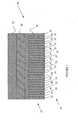
- FIG. 1is a cross-sectional view schematic drawing of a portion of a substrate including a strained semiconductor layer, an oxide layer and a base layer in accordance with an exemplary embodiment
- FIG. 2is a cross-sectional view of the portion illustrated in FIG. 1 , showing an etching step
- FIG. 3is a cross-sectional view of the portion illustrated in FIG. 2 , showing a deposition step
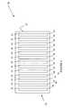
- FIG. 4is a bottom view of the portion illustrated in FIG. 1 ;
- FIG. 5is a bottom view schematic drawing of another portion of a substrate in accordance with another embodiment
- FIG. 6is a bottom view schematic drawing of yet another portion of a substrate in accordance with another embodiment
- FIG. 7is a general flow diagram showing a process for fabricating the portion illustrated in FIG. 1 ;
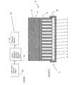
- FIG. 8is a cross-sectional view of the portion illustrated in FIG. 1 , showing a mechanical compression system attached to the substrate.
- FIGS. 1-8illustrate substrates and processes for providing a strained semiconductor layer, such as a strained silicon layer.
- the structures and processescan be utilized without requiring germanium doping or be utilized in conjunction with germanium doping.
- a portion 20 of an integrated circuitcan be part of a wafer or substrate, such as a semiconductor-on-insulator (SOI) substrate.
- Portion 20can be formed in a process 100 ( FIG. 7 ) and is preferably for use in a strained metal oxide semiconductor (SMOS) application.
- SMOSstrained metal oxide semiconductor
- Portion 20includes a substrate comprised of a strained layer 50 , a buried oxide layer 40 , and a base layer 30 .
- Layer 50can include germanium or be provided over a layer including germanium.
- a support substratecan be provided beneath layer 30 .
- base layer 30is a single crystalline silicon layer.
- Layer 30can be 400-1000 microns thick.
- Buried oxide layer 40can be a silicon dioxide layer.
- Layer 40can be 500-2000 ⁇ thick.
- Strained layer 50is preferably silicon or silicon/germanium (10 to 30% germanium). Layer 50 can be approximately 500 ⁇ thick.
- Layer 50is preferably under tensile stress due to a set 32 of trenches 36 ( FIG. 2 ) including a compressive material 34 .
- set 32 of trenches 36can be empty and the absence of material associated with the trenches causes tensile stress less in layer 50 .
- set 32 of trenches 36are filled with compressive material 34 such as a plasma enhanced chemical vapor deposition (PECVD) silicon nitride (SiN) material, a metal, or other material which becomes compressed upon or after depositing in set 32 of trenches 36 .
- PECVDplasma enhanced chemical vapor deposition
- SiNsilicon nitride
- a thermally-formed silicon nitride (SiN) material or low pressure chemical vapor deposition (LPCVD) SiN materialcan be utilized instead of plasma enhanced chemical vapor deposition (PECVD) SiN which causes compressive stress.
- SiNsilicon nitride
- LPCVDlow pressure chemical vapor deposition
- PECVDplasma enhanced chemical vapor deposition
- the compressive stress on layer 30is transferred through layer 40 to layer 50 as a tensile stress.
- Compressing layer 30 of portion 20stretches layers 40 and 50 .
- layer 40is not present and layer 50 is directly above layer 30 .
- layer 30can operate as a bulk substrate wherein a top surface is used for the active region. The top surface is under tensile stress due to the compressed strain at the bottom surface associated with set 32 of trenches 36 .
- set 32 of trenches 36correspond to the size of active regions in layer 50 .
- the same mask used to define active regions above layer 50can be used to define set 32 of trenches 36 .
- Some trenches 36can be larger than other trenches. For example, small trenches at certain locations may be necessary to maintain the integrity of the entire wafer.
- Compressive material 34preferably extends approximately 700 angstroms from a bottom surface of layer 30 towards layer 40 .
- set 32 of trenches 36extend all the way to layer 40 (e.g., trenches 36 reach bottom surface of layer 40 ).
- trenches 36extend to a distance 75% of the depth of layer 30 .
- trenches 36are 500-700 microns deep.
- layer 40 , layer 50 and layer 30are present on portion 20 before set 32 of trenches 36 is formed.
- trenches 36have a width of from 500-2000 angstroms and a length of several microns.
- Set 32 of trenches 36can have a tapered shape.
- trenches 36can have a trapezoidal cross-sectional shape with the narrower portion being closer to layer 40 .
- pillars 35can be preferably have a width slightly larger than the width of trenches 36 .
- the length of pillars 35can also be slightly longer or the same as the length of trenches 36 .
- portion 20is described as follows.
- set 32 of trenches 36are etched in a photolithographic process.
- a pad oxide layer and silicon nitride hard maskcan be used to form trenches 36 .
- An active layer photolithographic maskcan be utilized to define trenches 36 .
- the regions of the active layer photolithographic mask corresponding to the isolation trench on layer 50correspond to the position of trenches 36 on the back side of the IC wafer.
- Trenches 36are preferably etched in a dry etching process selective to layer 30 (e.g., silicon) with respect to the material of layer 40 (e.g., silicon dioxide).
- Set 32 of trenches 36are etched in a backside of layer 30 of the IC wafer.
- the etching processcan be a timed etching process to determine the depth of trenches 36 .
- the etching processcan reach layer 40 and stop at layer 40 .
- Alternative trench formation processescan be utilized to form trenches 36 .
- Pillars 35are formed after layers 50 and 40 are disposed above layer 30 . Pillars 35 are preferably the same material as layer 30 (e.g. silicon).
- compressive material 38fills trenches 36 ( FIG. 2 ) in a step 104 of process 100 .
- a compressive materialsuch as a compressive material including silicon nitride fills trenches 36 and then shrinks to pull pillars 35 associated with trenches 36 towards each other.
- the compressive materialcreates a compressive strain in layer 40 which provides a tensile strain on layers 40 and 50 above it.
- Material 38can be a compressive metal or a nitride material.
- material 38is PECVD silicon nitride.
- Material 38can be deposited in a conformal layer deposition process such as by plasma enhanced chemical vapor deposition or sputter deposition. Material 38 preferably has a thickness greater than or equal to one half the width associates with trenches 36 or 250-1000 Angstroms (A) or more thick in a preferred embodiment Angstroms thick.
- the deposition parameters of material 38can be Silane (SiH4)+Ammonia (NH3)+Nitrogen (N2) using a pressure of 10-1000 MilliTorr, an rf power of 10-1000 W, and a temperature of 100-500 C.
- material 38naturally compresses after deposition.
- material 38( FIG. 3 ) is planarized in a step 106 of process 1 00 to leave material 34 between set 33 of pillars 35 associated with set 32 of trenches 36 .
- Material 38can be planarized in a chemical mechanical polishing process or other etching process.
- set 32 of trenches 36can have a rectangular shape.
- trenches 36 including material 34have a square shape or a rectangular shape with an aspect ratio relatively close to one.
- the pattern of material 34is provided at an angle with respect to the lateral and top sides of layer 30 shown in FIG. 6 .
- set of trenches 36 including material 34are provided in a waffle pattern.
- set 32 of trenches 36can include trenches of various sizes. Some trenches and pillars in layer 30 can be smaller or larger than others depending upon design criteria. For example, an IC wafer may be required to be stronger at certain portions and have smaller trenches in particular regions for integrity. Further, the patterns shown in FIGS. 4-6 can be reversed with the locations for trenches 36 (material 34 ) being switched with the locations for pillars 35 .
- portion 20is provided with a mechanical system for additional compressive stress.
- trenches 36can be emptied or filled with material 34 .
- System 58can be a spring or clip.
- system 58is provided as part of an IC package utilized to house portion 20 .
- material 38can be a low thermal resistance material to increase heat flow from portion 20 .
- Low thermal resistance materialsinclude silicon and/or metal.
Landscapes
- Engineering & Computer Science (AREA)
- Physics & Mathematics (AREA)
- Condensed Matter Physics & Semiconductors (AREA)
- General Physics & Mathematics (AREA)
- Manufacturing & Machinery (AREA)
- Computer Hardware Design (AREA)
- Microelectronics & Electronic Packaging (AREA)
- Power Engineering (AREA)
- Chemical & Material Sciences (AREA)
- Materials Engineering (AREA)
- Element Separation (AREA)
Abstract
Description
- The present invention is related to integrated circuit (IC) substrates or wafers and to processes of making IC substrates or wafers. More particularly, the present invention relates to a method of forming strained semiconductor structures on substrates and to strained semiconductor structures or layers.
- Strained metal oxide semiconductor (SMOS) processes are utilized to increase transistor (MOSFET) performance by increasing the carrier mobility of silicon, thereby reducing resistance and power consumption and increasing drive current, frequency response and operating speed. Strained silicon is typically formed by growing a layer of silicon on a silicon germanium substrate or layer.
- The silicon germanium lattice associated with the silicon germanium substrate is generally more widely spaced than a pure silicon lattice, with spacing becoming wider with a higher percentage of germanium. Because the silicon lattice aligns with the larger silicon germanium lattice, a tensile strain is created in the silicon layer. The silicon atoms are essentially pulled apart from one another.
- Relaxed silicon has a conductive band that contains six equal valence bands. The application of tensile strain to the silicon causes four of the valence bands to increase in energy and two of the valence bands to decrease in energy. As a result of quantum effects, electrons effectively weigh 30 percent less when passing through the lower energy bands. Thus, the lower energy bands offer less resistance to electron flow. In addition, electrons meet with less vibrational energy from the nucleus of the silicon atom, which causes them to scatter at a rate of 500 to 1000 times less than in relaxed silicon. As a result, carrier mobility is dramatically increased in strained silicon compared to relaxed silicon, providing an increase in mobility of 80% or more for electrons and 20% or more for holes. The increase in mobility has been found to persist for current fields up to 1.5 megavolts/centimeter. These factors are believed to enable a device speed increase of 35% without further reduction of device size, or a 25% reduction in power consumption without a reduction in performance.
- Conventional SOI substrates have included a strained silicon layer above a buried oxide layer above a base layer. The buried oxide layer can be formed in a variety of processes including deposition above the base layer or by doping the base layer with oxygen. The strained semiconductor layer can be formed by providing a silicon germanium layer having a composition of Si(1-x)Gex, where x is approximately 0.2, and is more generally in the range of 0.1-0.3. The silicon germanium layer can be deposited by chemical vapor deposition using silane and germane. The concentration of germane can be decreased as deposition occurs so that the upper most part of the silicon germanium layer is mostly or all silicon.
- The use of germanium in SMOS processes can cause germanium contamination problems for IC structures, layers, and equipment. In particular, germanium outgassing or outdiffusion can contaminate various components associated with the fabrication equipment and integrated circuit structures associating with the processed wafer. Further, germanium outgassing can negatively impact the formation of thin films. In addition, germanium outdiffusion can cause germanium accumulation or “pile-up” at the interface of the liner, thereby causing reliability issues for the STI structure.
- Germanium outgassing can be particularly problematic at the very high temperatures and HCI ambient environments associated with the liner of a shallow trench isolation (STI) structure. For example, conventional STI liner oxide processes can utilize temperatures of approximately 1000° C. which enhance germanium outgassing.
- Thus, there is a need for a strained semiconductor substrate which can be formed without using germanium. Further still, there is a need for a process of forming high quality SMOS substrates. Further still, there is a need for an SMOS wafer formation process that does not require strained layer deposition. Yet further, there is a need for a substrate that is not as susceptible to germanium outgassing. Further still, there is a need for new process of forming strained semiconductor layers. Even further, there is a need for a wafer process that enhances and/or increases the longevity of the strained characteristic of a layer.
- An exemplary embodiment relates to a method of manufacturing an integrated circuit substrate. The integrated circuit substrate includes a strained layer. The method includes providing a base layer, providing an insulating layer above the base layer, and providing a semiconductor layer above the insulating layer. The method further includes forming pillars in the base layer.
- Another exemplary embodiment relates to a method of forming a strained semiconductor layer above a base layer. The method includes etching trenches in the base layer and providing a compressive material in the trenches.
- Still another exemplary embodiment relates to a substrate. The substrate includes a strained layer and a base layer below the strained layer. The base layer has trenches on a side opposite the strained layer. The trenches induce stress in the strained layer.
- Exemplary embodiments will become more fully understood from the following detailed description, taken in conjunction with the accompanying drawings, wherein like reference numerals refer to like parts, and wherein:
FIG. 1 is a cross-sectional view schematic drawing of a portion of a substrate including a strained semiconductor layer, an oxide layer and a base layer in accordance with an exemplary embodiment;FIG. 2 is a cross-sectional view of the portion illustrated inFIG. 1 , showing an etching step;FIG. 3 is a cross-sectional view of the portion illustrated inFIG. 2 , showing a deposition step;FIG. 4 is a bottom view of the portion illustrated inFIG. 1 ;FIG. 5 is a bottom view schematic drawing of another portion of a substrate in accordance with another embodiment;FIG. 6 is a bottom view schematic drawing of yet another portion of a substrate in accordance with another embodiment;FIG. 7 is a general flow diagram showing a process for fabricating the portion illustrated inFIG. 1 ; andFIG. 8 is a cross-sectional view of the portion illustrated inFIG. 1 , showing a mechanical compression system attached to the substrate.FIGS. 1-8 illustrate substrates and processes for providing a strained semiconductor layer, such as a strained silicon layer. The structures and processes can be utilized without requiring germanium doping or be utilized in conjunction with germanium doping.- Referring to
FIG. 1 , aportion 20 of an integrated circuit (IC) can be part of a wafer or substrate, such as a semiconductor-on-insulator (SOI) substrate.Portion 20 can be formed in a process100 (FIG. 7 ) and is preferably for use in a strained metal oxide semiconductor (SMOS) application. Portion 20 includes a substrate comprised of astrained layer 50, a buriedoxide layer 40, and abase layer 30.Layer 50 can include germanium or be provided over a layer including germanium. In addition, a support substrate can be provided beneathlayer 30.- In one embodiment,
base layer 30 is a single crystalline silicon layer.Layer 30 can be 400-1000 microns thick.Buried oxide layer 40 can be a silicon dioxide layer.Layer 40 can be 500-2000 Å thick.Strained layer 50 is preferably silicon or silicon/germanium (10 to 30% germanium).Layer 50 can be approximately 500 Å thick. Layer 50 is preferably under tensile stress due to aset 32 of trenches36 (FIG. 2 ) including acompressive material 34. In one embodiment, set32 oftrenches 36 can be empty and the absence of material associated with the trenches causes tensile stress less inlayer 50. Preferably, set32 oftrenches 36 are filled withcompressive material 34 such as a plasma enhanced chemical vapor deposition (PECVD) silicon nitride (SiN) material, a metal, or other material which becomes compressed upon or after depositing inset 32 oftrenches 36. If tensile stress is desired intrenches 36, a thermally-formed silicon nitride (SiN) material or low pressure chemical vapor deposition (LPCVD) SiN material can be utilized instead of plasma enhanced chemical vapor deposition (PECVD) SiN which causes compressive stress.- The compressive stress on
layer 30 is transferred throughlayer 40 to layer50 as a tensile stress. Compressinglayer 30 ofportion 20 stretches layers40 and50. In an alternative embodiment,layer 40 is not present andlayer 50 is directly abovelayer 30. In yet another embodiment,layer 30 can operate as a bulk substrate wherein a top surface is used for the active region. The top surface is under tensile stress due to the compressed strain at the bottom surface associated withset 32 oftrenches 36. - In one embodiment, set32 of
trenches 36 correspond to the size of active regions inlayer 50. In one embodiment, the same mask used to define active regions abovelayer 50 can be used to define set32 oftrenches 36. Sometrenches 36 can be larger than other trenches. For example, small trenches at certain locations may be necessary to maintain the integrity of the entire wafer. Compressive material 34 preferably extends approximately 700 angstroms from a bottom surface oflayer 30 towardslayer 40. In one embodiment, set32 oftrenches 36 extend all the way to layer40 (e.g.,trenches 36 reach bottom surface of layer40). In another embodiment,trenches 36 extend to a distance 75% of the depth oflayer 30. Preferably,trenches 36 are 500-700 microns deep. Preferably,layer 40,layer 50 andlayer 30 are present onportion 20 before set32 oftrenches 36 is formed.- Preferably,
trenches 36 have a width of from 500-2000 angstroms and a length of several microns. Set32 oftrenches 36 can have a tapered shape. For example,trenches 36 can have a trapezoidal cross-sectional shape with the narrower portion being closer tolayer 40. If set33 ofpillars 35 are disposed betweentrenches 32,pillars 35 can be preferably have a width slightly larger than the width oftrenches 36. The length ofpillars 35 can also be slightly longer or the same as the length oftrenches 36. - With reference to
FIG. 7 andFIGS. 1-3 , the formation ofportion 20 is described as follows. InFIG. 2 , set32 oftrenches 36 are etched in a photolithographic process. A pad oxide layer and silicon nitride hard mask can be used to formtrenches 36. - An active layer photolithographic mask can be utilized to define
trenches 36. The regions of the active layer photolithographic mask corresponding to the isolation trench onlayer 50 correspond to the position oftrenches 36 on the back side of the IC wafer. Trenches 36 are preferably etched in a dry etching process selective to layer30 (e.g., silicon) with respect to the material of layer40 (e.g., silicon dioxide). Set32 oftrenches 36 are etched in a backside oflayer 30 of the IC wafer. The etching process can be a timed etching process to determine the depth oftrenches 36. Alternatively, the etching process can reachlayer 40 and stop atlayer 40. Alternative trench formation processes can be utilized to formtrenches 36.- Formation of
set 32 oftrenches 36 leaves set33 ofpillars 35 inlayer 30.Pillars 35 are formed afterlayers layer 30.Pillars 35 are preferably the same material as layer30 (e.g. silicon). - With reference to
FIG. 3 ,compressive material 38 fills trenches36 (FIG. 2 ) in astep 104 ofprocess 100. Preferably, a compressive material, such as a compressive material including silicon nitride fillstrenches 36 and then shrinks to pullpillars 35 associated withtrenches 36 towards each other. The compressive material creates a compressive strain inlayer 40 which provides a tensile strain onlayers Material 38 can be a compressive metal or a nitride material. In one embodiment,material 38 is PECVD silicon nitride.Material 38 can be deposited in a conformal layer deposition process such as by plasma enhanced chemical vapor deposition or sputter deposition.Material 38 preferably has a thickness greater than or equal to one half the width associates withtrenches 36 or 250-1000 Angstroms (A) or more thick in a preferred embodiment Angstroms thick. For SiN, the deposition parameters ofmaterial 38 can be Silane (SiH4)+Ammonia (NH3)+Nitrogen (N2) using a pressure of 10-1000 MilliTorr, an rf power of 10-1000 W, and a temperature of 100-500 C. Preferably,material 38 naturally compresses after deposition.- With reference to
FIG. 1 , material38 (FIG. 3 ) is planarized in astep 106 of process100 to leavematerial 34 betweenset 33 ofpillars 35 associated withset 32 oftrenches 36.Material 38 can be planarized in a chemical mechanical polishing process or other etching process. - With reference to
FIG. 4 , set32 oftrenches 36 can have a rectangular shape. In accordance with another embodiment inFIG. 5 ,trenches 36 includingmaterial 34 have a square shape or a rectangular shape with an aspect ratio relatively close to one. In another embodiment, the pattern ofmaterial 34 is provided at an angle with respect to the lateral and top sides oflayer 30 shown inFIG. 6 . - In one embodiment, set of
trenches 36 includingmaterial 34 are provided in a waffle pattern. As discussed above with reference toFIG. 1 , set32 oftrenches 36 can include trenches of various sizes. Some trenches and pillars inlayer 30 can be smaller or larger than others depending upon design criteria. For example, an IC wafer may be required to be stronger at certain portions and have smaller trenches in particular regions for integrity. Further, the patterns shown inFIGS. 4-6 can be reversed with the locations for trenches36 (material34) being switched with the locations forpillars 35. - With reference to
FIG. 8 ,portion 20 is provided with a mechanical system for additional compressive stress. In this embodiment,trenches 36 can be emptied or filled withmaterial 34.System 58 can be a spring or clip. In one embodiment,system 58 is provided as part of an IC package utilized tohouse portion 20. - In another embodiment,
material 38 can be a low thermal resistance material to increase heat flow fromportion 20. Low thermal resistance materials include silicon and/or metal. - It is understood that while the detailed drawings, specific examples, and particular values given provide a preferred exemplary embodiment of the present invention, it is for the purpose of illustration only. The patterns, shapes and sizes of trenches and pillars are not disclosed in a limiting fashion. The method and apparatus of the invention is not limited to the precise details and conditions disclosed. Various changes may be made to the details disclosed without departing from the spirit of the invention, which is defined by the following claims.
Claims (21)
Priority Applications (8)
| Application Number | Priority Date | Filing Date | Title |
|---|---|---|---|
| US10/729,479US7144818B2 (en) | 2003-12-05 | 2003-12-05 | Semiconductor substrate and processes therefor |
| JP2006542572AJP2007513517A (en) | 2003-12-05 | 2004-10-26 | Strained semiconductor substrate and manufacturing process thereof |
| PCT/US2004/035417WO2005062357A1 (en) | 2003-12-05 | 2004-10-26 | Strained semiconductor substrate and processes therefor |
| EP04796404AEP1690288A1 (en) | 2003-12-05 | 2004-10-26 | Strained semiconductor substrate and processes therefor |
| KR1020067011087AKR101086896B1 (en) | 2003-12-05 | 2004-10-26 | Modified semiconductor substrate and its process |
| CN2004800358158ACN1890784B (en) | 2003-12-05 | 2004-10-26 | Strained semiconductor substrate and processes therefor |
| TW093137307ATWI369737B (en) | 2003-12-05 | 2004-12-03 | Strained semiconductor substrate and processes therefor |
| US11/179,282US7265420B2 (en) | 2003-12-05 | 2005-07-12 | Semiconductor substrate layer configured for inducement of compressive or expansive force |
Applications Claiming Priority (1)
| Application Number | Priority Date | Filing Date | Title |
|---|---|---|---|
| US10/729,479US7144818B2 (en) | 2003-12-05 | 2003-12-05 | Semiconductor substrate and processes therefor |
Related Child Applications (1)
| Application Number | Title | Priority Date | Filing Date |
|---|---|---|---|
| US11/179,282DivisionUS7265420B2 (en) | 2003-12-05 | 2005-07-12 | Semiconductor substrate layer configured for inducement of compressive or expansive force |
Publications (2)
| Publication Number | Publication Date |
|---|---|
| US20050124170A1true US20050124170A1 (en) | 2005-06-09 |
| US7144818B2 US7144818B2 (en) | 2006-12-05 |
Family
ID=34633951
Family Applications (2)
| Application Number | Title | Priority Date | Filing Date |
|---|---|---|---|
| US10/729,479Expired - LifetimeUS7144818B2 (en) | 2003-12-05 | 2003-12-05 | Semiconductor substrate and processes therefor |
| US11/179,282Expired - LifetimeUS7265420B2 (en) | 2003-12-05 | 2005-07-12 | Semiconductor substrate layer configured for inducement of compressive or expansive force |
Family Applications After (1)
| Application Number | Title | Priority Date | Filing Date |
|---|---|---|---|
| US11/179,282Expired - LifetimeUS7265420B2 (en) | 2003-12-05 | 2005-07-12 | Semiconductor substrate layer configured for inducement of compressive or expansive force |
Country Status (7)
| Country | Link |
|---|---|
| US (2) | US7144818B2 (en) |
| EP (1) | EP1690288A1 (en) |
| JP (1) | JP2007513517A (en) |
| KR (1) | KR101086896B1 (en) |
| CN (1) | CN1890784B (en) |
| TW (1) | TWI369737B (en) |
| WO (1) | WO2005062357A1 (en) |
Cited By (12)
| Publication number | Priority date | Publication date | Assignee | Title |
|---|---|---|---|---|
| US20070007508A1 (en)* | 2003-06-26 | 2007-01-11 | Rj Mears, Llc | Semiconductor Device Including a Strained Superlattice Layer Above a Stress Layer |
| US20070010040A1 (en)* | 2003-06-26 | 2007-01-11 | Rj Mears, Llc | Method for Making a Semiconductor Device Including a Strained Superlattice Layer Above a Stress Layer |
| WO2007011627A1 (en)* | 2005-07-15 | 2007-01-25 | Mears Technologies, Inc. | Semiconductor device including a strained superlattice layer above a stress layer and associated methods |
| US20070063185A1 (en)* | 2003-06-26 | 2007-03-22 | Rj Mears, Llc | Semiconductor device including a front side strained superlattice layer and a back side stress layer |
| US20070063186A1 (en)* | 2003-06-26 | 2007-03-22 | Rj Mears, Llc | Method for making a semiconductor device including a front side strained superlattice layer and a back side stress layer |
| EP2937898A1 (en)* | 2009-07-15 | 2015-10-28 | Silanna Semiconductor U.S.A., Inc. | Semiconductor-on-insulator with backside heat dissipation |
| US9368468B2 (en) | 2009-07-15 | 2016-06-14 | Qualcomm Switch Corp. | Thin integrated circuit chip-on-board assembly |
| US9390974B2 (en) | 2012-12-21 | 2016-07-12 | Qualcomm Incorporated | Back-to-back stacked integrated circuit assembly and method of making |
| US9466719B2 (en) | 2009-07-15 | 2016-10-11 | Qualcomm Incorporated | Semiconductor-on-insulator with back side strain topology |
| US9496227B2 (en) | 2009-07-15 | 2016-11-15 | Qualcomm Incorporated | Semiconductor-on-insulator with back side support layer |
| US9515181B2 (en) | 2014-08-06 | 2016-12-06 | Qualcomm Incorporated | Semiconductor device with self-aligned back side features |
| DE102006007293B4 (en) | 2006-01-31 | 2023-04-06 | OSRAM Opto Semiconductors Gesellschaft mit beschränkter Haftung | Method for producing a quasi-substrate wafer and a semiconductor body produced using such a quasi-substrate wafer |
Families Citing this family (9)
| Publication number | Priority date | Publication date | Assignee | Title |
|---|---|---|---|---|
| US20070020860A1 (en)* | 2003-06-26 | 2007-01-25 | Rj Mears, Llc | Method for Making Semiconductor Device Including a Strained Superlattice and Overlying Stress Layer and Related Methods |
| US20070020833A1 (en)* | 2003-06-26 | 2007-01-25 | Rj Mears, Llc | Method for Making a Semiconductor Device Including a Channel with a Non-Semiconductor Layer Monolayer |
| US20070015344A1 (en)* | 2003-06-26 | 2007-01-18 | Rj Mears, Llc | Method for Making a Semiconductor Device Including a Strained Superlattice Between at Least One Pair of Spaced Apart Stress Regions |
| US7598515B2 (en)* | 2003-06-26 | 2009-10-06 | Mears Technologies, Inc. | Semiconductor device including a strained superlattice and overlying stress layer and related methods |
| US7531828B2 (en)* | 2003-06-26 | 2009-05-12 | Mears Technologies, Inc. | Semiconductor device including a strained superlattice between at least one pair of spaced apart stress regions |
| US7144818B2 (en)* | 2003-12-05 | 2006-12-05 | Advanced Micro Devices, Inc. | Semiconductor substrate and processes therefor |
| JP5055846B2 (en)* | 2006-06-09 | 2012-10-24 | ソニー株式会社 | Semiconductor device and manufacturing method thereof |
| CN102420253A (en)* | 2011-12-13 | 2012-04-18 | 清华大学 | Vertical dual-diffusion metal oxide semiconductor (VDMOS) device with back surface embedded into strain medium region, and manufacturing method for VDMOS device |
| CN111883418B (en)* | 2020-08-05 | 2021-04-27 | 长江存储科技有限责任公司 | Manufacturing method of semiconductor structure |
Citations (8)
| Publication number | Priority date | Publication date | Assignee | Title |
|---|---|---|---|---|
| US4597166A (en)* | 1982-02-10 | 1986-07-01 | Tokyo Shibaura Denki Kabushiki Kaisha | Semiconductor substrate and method for manufacturing semiconductor device using the same |
| US5294559A (en)* | 1990-07-30 | 1994-03-15 | Texas Instruments Incorporated | Method of forming a vertical transistor |
| US20020046985A1 (en)* | 2000-03-24 | 2002-04-25 | Daneman Michael J. | Process for creating an electrically isolated electrode on a sidewall of a cavity in a base |
| US6593191B2 (en)* | 2000-05-26 | 2003-07-15 | Amberwave Systems Corporation | Buried channel strained silicon FET using a supply layer created through ion implantation |
| US6677204B2 (en)* | 2000-08-14 | 2004-01-13 | Matrix Semiconductor, Inc. | Multigate semiconductor device with vertical channel current and method of fabrication |
| US6707106B1 (en)* | 2002-10-18 | 2004-03-16 | Advanced Micro Devices, Inc. | Semiconductor device with tensile strain silicon introduced by compressive material in a buried oxide layer |
| US6803631B2 (en)* | 2003-01-23 | 2004-10-12 | Advanced Micro Devices, Inc. | Strained channel finfet |
| US6835246B2 (en)* | 2001-11-16 | 2004-12-28 | Saleem H. Zaidi | Nanostructures for hetero-expitaxial growth on silicon substrates |
Family Cites Families (11)
| Publication number | Priority date | Publication date | Assignee | Title |
|---|---|---|---|---|
| JPS61181931A (en) | 1985-02-08 | 1986-08-14 | Fuji Electric Co Ltd | pressure sensor |
| JPH03201536A (en)* | 1989-12-28 | 1991-09-03 | Mitsubishi Electric Corp | Manufacture of semiconductor device |
| JP2803321B2 (en) | 1990-04-27 | 1998-09-24 | 株式会社デンソー | Semiconductor strain sensor |
| JP2728310B2 (en)* | 1990-07-30 | 1998-03-18 | シャープ株式会社 | Semiconductor wafer gettering method |
| JPH04245640A (en) | 1991-01-31 | 1992-09-02 | Kawasaki Steel Corp | Processing method of semiconductor substrate |
| JP2824818B2 (en)* | 1991-08-02 | 1998-11-18 | キヤノン株式会社 | Active matrix liquid crystal display |
| JPH05198783A (en) | 1992-01-23 | 1993-08-06 | Hitachi Ltd | Manufacture of semiconductor integrated circuit device |
| US6191432B1 (en)* | 1996-09-02 | 2001-02-20 | Kabushiki Kaisha Toshiba | Semiconductor device and memory device |
| US6900521B2 (en)* | 2002-06-10 | 2005-05-31 | Micron Technology, Inc. | Vertical transistors and output prediction logic circuits containing same |
| JP2004228273A (en)* | 2003-01-22 | 2004-08-12 | Renesas Technology Corp | Semiconductor device |
| US7144818B2 (en)* | 2003-12-05 | 2006-12-05 | Advanced Micro Devices, Inc. | Semiconductor substrate and processes therefor |
- 2003
- 2003-12-05USUS10/729,479patent/US7144818B2/ennot_activeExpired - Lifetime
- 2004
- 2004-10-26EPEP04796404Apatent/EP1690288A1/ennot_activeWithdrawn
- 2004-10-26WOPCT/US2004/035417patent/WO2005062357A1/enactiveApplication Filing
- 2004-10-26KRKR1020067011087Apatent/KR101086896B1/ennot_activeExpired - Fee Related
- 2004-10-26JPJP2006542572Apatent/JP2007513517A/enactivePending
- 2004-10-26CNCN2004800358158Apatent/CN1890784B/ennot_activeExpired - Fee Related
- 2004-12-03TWTW093137307Apatent/TWI369737B/ennot_activeIP Right Cessation
- 2005
- 2005-07-12USUS11/179,282patent/US7265420B2/ennot_activeExpired - Lifetime
Patent Citations (8)
| Publication number | Priority date | Publication date | Assignee | Title |
|---|---|---|---|---|
| US4597166A (en)* | 1982-02-10 | 1986-07-01 | Tokyo Shibaura Denki Kabushiki Kaisha | Semiconductor substrate and method for manufacturing semiconductor device using the same |
| US5294559A (en)* | 1990-07-30 | 1994-03-15 | Texas Instruments Incorporated | Method of forming a vertical transistor |
| US20020046985A1 (en)* | 2000-03-24 | 2002-04-25 | Daneman Michael J. | Process for creating an electrically isolated electrode on a sidewall of a cavity in a base |
| US6593191B2 (en)* | 2000-05-26 | 2003-07-15 | Amberwave Systems Corporation | Buried channel strained silicon FET using a supply layer created through ion implantation |
| US6677204B2 (en)* | 2000-08-14 | 2004-01-13 | Matrix Semiconductor, Inc. | Multigate semiconductor device with vertical channel current and method of fabrication |
| US6835246B2 (en)* | 2001-11-16 | 2004-12-28 | Saleem H. Zaidi | Nanostructures for hetero-expitaxial growth on silicon substrates |
| US6707106B1 (en)* | 2002-10-18 | 2004-03-16 | Advanced Micro Devices, Inc. | Semiconductor device with tensile strain silicon introduced by compressive material in a buried oxide layer |
| US6803631B2 (en)* | 2003-01-23 | 2004-10-12 | Advanced Micro Devices, Inc. | Strained channel finfet |
Cited By (18)
| Publication number | Priority date | Publication date | Assignee | Title |
|---|---|---|---|---|
| US20070007508A1 (en)* | 2003-06-26 | 2007-01-11 | Rj Mears, Llc | Semiconductor Device Including a Strained Superlattice Layer Above a Stress Layer |
| US20070010040A1 (en)* | 2003-06-26 | 2007-01-11 | Rj Mears, Llc | Method for Making a Semiconductor Device Including a Strained Superlattice Layer Above a Stress Layer |
| US20070063185A1 (en)* | 2003-06-26 | 2007-03-22 | Rj Mears, Llc | Semiconductor device including a front side strained superlattice layer and a back side stress layer |
| US20070063186A1 (en)* | 2003-06-26 | 2007-03-22 | Rj Mears, Llc | Method for making a semiconductor device including a front side strained superlattice layer and a back side stress layer |
| US7612366B2 (en) | 2003-06-26 | 2009-11-03 | Mears Technologies, Inc. | Semiconductor device including a strained superlattice layer above a stress layer |
| WO2007011627A1 (en)* | 2005-07-15 | 2007-01-25 | Mears Technologies, Inc. | Semiconductor device including a strained superlattice layer above a stress layer and associated methods |
| WO2007038656A1 (en)* | 2005-09-26 | 2007-04-05 | Mears Technologies, Inc. | Semiconductor device including a front side strained superlattice layer and a back side stress layer and associated methods |
| DE102006007293B4 (en) | 2006-01-31 | 2023-04-06 | OSRAM Opto Semiconductors Gesellschaft mit beschränkter Haftung | Method for producing a quasi-substrate wafer and a semiconductor body produced using such a quasi-substrate wafer |
| US9368468B2 (en) | 2009-07-15 | 2016-06-14 | Qualcomm Switch Corp. | Thin integrated circuit chip-on-board assembly |
| US9412644B2 (en) | 2009-07-15 | 2016-08-09 | Qualcomm Incorporated | Integrated circuit assembly and method of making |
| US9466719B2 (en) | 2009-07-15 | 2016-10-11 | Qualcomm Incorporated | Semiconductor-on-insulator with back side strain topology |
| US9496227B2 (en) | 2009-07-15 | 2016-11-15 | Qualcomm Incorporated | Semiconductor-on-insulator with back side support layer |
| US9748272B2 (en) | 2009-07-15 | 2017-08-29 | Qualcomm Incorporated | Semiconductor-on-insulator with back side strain inducing material |
| US10217822B2 (en) | 2009-07-15 | 2019-02-26 | Qualcomm Incorporated | Semiconductor-on-insulator with back side heat dissipation |
| EP2937898A1 (en)* | 2009-07-15 | 2015-10-28 | Silanna Semiconductor U.S.A., Inc. | Semiconductor-on-insulator with backside heat dissipation |
| US9390974B2 (en) | 2012-12-21 | 2016-07-12 | Qualcomm Incorporated | Back-to-back stacked integrated circuit assembly and method of making |
| US9576937B2 (en) | 2012-12-21 | 2017-02-21 | Qualcomm Incorporated | Back-to-back stacked integrated circuit assembly |
| US9515181B2 (en) | 2014-08-06 | 2016-12-06 | Qualcomm Incorporated | Semiconductor device with self-aligned back side features |
Also Published As
| Publication number | Publication date |
|---|---|
| TWI369737B (en) | 2012-08-01 |
| US7265420B2 (en) | 2007-09-04 |
| CN1890784A (en) | 2007-01-03 |
| CN1890784B (en) | 2013-04-24 |
| US7144818B2 (en) | 2006-12-05 |
| KR20060121136A (en) | 2006-11-28 |
| US20050263753A1 (en) | 2005-12-01 |
| WO2005062357A1 (en) | 2005-07-07 |
| JP2007513517A (en) | 2007-05-24 |
| TW200525641A (en) | 2005-08-01 |
| KR101086896B1 (en) | 2011-11-25 |
| EP1690288A1 (en) | 2006-08-16 |
Similar Documents
| Publication | Publication Date | Title |
|---|---|---|
| US7265420B2 (en) | Semiconductor substrate layer configured for inducement of compressive or expansive force | |
| US7701019B2 (en) | Tensile strained substrate | |
| US7560328B2 (en) | Strained Si on multiple materials for bulk or SOI substrates | |
| US7687829B2 (en) | Stressed field effect transistors on hybrid orientation substrate | |
| US9112029B2 (en) | Strained transistor integration for CMOS | |
| US6852600B1 (en) | Strained silicon MOSFET having silicon source/drain regions and method for its fabrication | |
| US6800910B2 (en) | FinFET device incorporating strained silicon in the channel region | |
| US7550758B2 (en) | Method for providing a nanoscale, high electron mobility transistor (HEMT) on insulator | |
| US20070257249A1 (en) | Silicon/silcion germaninum/silicon body device with embedded carbon dopant | |
| WO2012100396A1 (en) | Semiconductor device and method for manufacturing same | |
| US20080213952A1 (en) | Shallow trench isolation process and structure with minimized strained silicon consumption | |
| US7202139B2 (en) | MOSFET device with a strained channel | |
| US7012007B1 (en) | Strained silicon MOSFET having improved thermal conductivity and method for its fabrication | |
| US6900143B1 (en) | Strained silicon MOSFETs having improved thermal dissipation |
Legal Events
| Date | Code | Title | Description |
|---|---|---|---|
| AS | Assignment | Owner name:ADVANCED MICRO DEVICES, INC., CALIFORNIA Free format text:ASSIGNMENT OF ASSIGNORS INTEREST;ASSIGNORS:PELELLA, MARIO M.;CHAN, SIMON S.;REEL/FRAME:014780/0303 Effective date:20031013 | |
| STCF | Information on status: patent grant | Free format text:PATENTED CASE | |
| CC | Certificate of correction | ||
| AS | Assignment | Owner name:GLOBALFOUNDRIES INC., CAYMAN ISLANDS Free format text:AFFIRMATION OF PATENT ASSIGNMENT;ASSIGNOR:ADVANCED MICRO DEVICES, INC.;REEL/FRAME:023119/0083 Effective date:20090630 | |
| FPAY | Fee payment | Year of fee payment:4 | |
| FPAY | Fee payment | Year of fee payment:8 | |
| MAFP | Maintenance fee payment | Free format text:PAYMENT OF MAINTENANCE FEE, 12TH YEAR, LARGE ENTITY (ORIGINAL EVENT CODE: M1553) Year of fee payment:12 | |
| AS | Assignment | Owner name:WILMINGTON TRUST, NATIONAL ASSOCIATION, DELAWARE Free format text:SECURITY AGREEMENT;ASSIGNOR:GLOBALFOUNDRIES INC.;REEL/FRAME:049490/0001 Effective date:20181127 | |
| AS | Assignment | Owner name:GLOBALFOUNDRIES U.S. INC., CALIFORNIA Free format text:ASSIGNMENT OF ASSIGNORS INTEREST;ASSIGNOR:GLOBALFOUNDRIES INC.;REEL/FRAME:054633/0001 Effective date:20201022 | |
| AS | Assignment | Owner name:GLOBALFOUNDRIES INC., CAYMAN ISLANDS Free format text:RELEASE BY SECURED PARTY;ASSIGNOR:WILMINGTON TRUST, NATIONAL ASSOCIATION;REEL/FRAME:054636/0001 Effective date:20201117 | |
| AS | Assignment | Owner name:GLOBALFOUNDRIES U.S. INC., NEW YORK Free format text:RELEASE BY SECURED PARTY;ASSIGNOR:WILMINGTON TRUST, NATIONAL ASSOCIATION;REEL/FRAME:056987/0001 Effective date:20201117 |