US20050124093A1 - Fan out type wafer level package structure and method of the same - Google Patents
Fan out type wafer level package structure and method of the sameDownload PDFInfo
- Publication number
- US20050124093A1 US20050124093A1US10/725,933US72593303AUS2005124093A1US 20050124093 A1US20050124093 A1US 20050124093A1US 72593303 AUS72593303 AUS 72593303AUS 2005124093 A1US2005124093 A1US 2005124093A1
- Authority
- US
- United States
- Prior art keywords
- layer
- dies
- conductive lines
- openings
- conductive
- Prior art date
- Legal status (The legal status is an assumption and is not a legal conclusion. Google has not performed a legal analysis and makes no representation as to the accuracy of the status listed.)
- Granted
Links
Images


Classifications
- H—ELECTRICITY
- H01—ELECTRIC ELEMENTS
- H01L—SEMICONDUCTOR DEVICES NOT COVERED BY CLASS H10
- H01L21/00—Processes or apparatus adapted for the manufacture or treatment of semiconductor or solid state devices or of parts thereof
- H01L21/02—Manufacture or treatment of semiconductor devices or of parts thereof
- H01L21/04—Manufacture or treatment of semiconductor devices or of parts thereof the devices having potential barriers, e.g. a PN junction, depletion layer or carrier concentration layer
- H01L21/50—Assembly of semiconductor devices using processes or apparatus not provided for in a single one of the groups H01L21/18 - H01L21/326 or H10D48/04 - H10D48/07 e.g. sealing of a cap to a base of a container
- H01L21/56—Encapsulations, e.g. encapsulation layers, coatings
- H01L21/561—Batch processing
- H—ELECTRICITY
- H01—ELECTRIC ELEMENTS
- H01L—SEMICONDUCTOR DEVICES NOT COVERED BY CLASS H10
- H01L23/00—Details of semiconductor or other solid state devices
- H01L23/48—Arrangements for conducting electric current to or from the solid state body in operation, e.g. leads, terminal arrangements ; Selection of materials therefor
- H—ELECTRICITY
- H01—ELECTRIC ELEMENTS
- H01L—SEMICONDUCTOR DEVICES NOT COVERED BY CLASS H10
- H01L23/00—Details of semiconductor or other solid state devices
- H01L23/28—Encapsulations, e.g. encapsulating layers, coatings, e.g. for protection
- H01L23/31—Encapsulations, e.g. encapsulating layers, coatings, e.g. for protection characterised by the arrangement or shape
- H01L23/3107—Encapsulations, e.g. encapsulating layers, coatings, e.g. for protection characterised by the arrangement or shape the device being completely enclosed
- H01L23/3121—Encapsulations, e.g. encapsulating layers, coatings, e.g. for protection characterised by the arrangement or shape the device being completely enclosed a substrate forming part of the encapsulation
- H01L23/3128—Encapsulations, e.g. encapsulating layers, coatings, e.g. for protection characterised by the arrangement or shape the device being completely enclosed a substrate forming part of the encapsulation the substrate having spherical bumps for external connection
- H—ELECTRICITY
- H01—ELECTRIC ELEMENTS
- H01L—SEMICONDUCTOR DEVICES NOT COVERED BY CLASS H10
- H01L23/00—Details of semiconductor or other solid state devices
- H01L23/52—Arrangements for conducting electric current within the device in operation from one component to another, i.e. interconnections, e.g. wires, lead frames
- H01L23/538—Arrangements for conducting electric current within the device in operation from one component to another, i.e. interconnections, e.g. wires, lead frames the interconnection structure between a plurality of semiconductor chips being formed on, or in, insulating substrates
- H01L23/5389—Arrangements for conducting electric current within the device in operation from one component to another, i.e. interconnections, e.g. wires, lead frames the interconnection structure between a plurality of semiconductor chips being formed on, or in, insulating substrates the chips being integrally enclosed by the interconnect and support structures
- H—ELECTRICITY
- H01—ELECTRIC ELEMENTS
- H01L—SEMICONDUCTOR DEVICES NOT COVERED BY CLASS H10
- H01L24/00—Arrangements for connecting or disconnecting semiconductor or solid-state bodies; Methods or apparatus related thereto
- H01L24/01—Means for bonding being attached to, or being formed on, the surface to be connected, e.g. chip-to-package, die-attach, "first-level" interconnects; Manufacturing methods related thereto
- H01L24/18—High density interconnect [HDI] connectors; Manufacturing methods related thereto
- H01L24/19—Manufacturing methods of high density interconnect preforms
- H—ELECTRICITY
- H01—ELECTRIC ELEMENTS
- H01L—SEMICONDUCTOR DEVICES NOT COVERED BY CLASS H10
- H01L24/00—Arrangements for connecting or disconnecting semiconductor or solid-state bodies; Methods or apparatus related thereto
- H01L24/01—Means for bonding being attached to, or being formed on, the surface to be connected, e.g. chip-to-package, die-attach, "first-level" interconnects; Manufacturing methods related thereto
- H01L24/18—High density interconnect [HDI] connectors; Manufacturing methods related thereto
- H01L24/20—Structure, shape, material or disposition of high density interconnect preforms
- H—ELECTRICITY
- H01—ELECTRIC ELEMENTS
- H01L—SEMICONDUCTOR DEVICES NOT COVERED BY CLASS H10
- H01L24/00—Arrangements for connecting or disconnecting semiconductor or solid-state bodies; Methods or apparatus related thereto
- H01L24/93—Batch processes
- H01L24/95—Batch processes at chip-level, i.e. with connecting carried out on a plurality of singulated devices, i.e. on diced chips
- H01L24/97—Batch processes at chip-level, i.e. with connecting carried out on a plurality of singulated devices, i.e. on diced chips the devices being connected to a common substrate, e.g. interposer, said common substrate being separable into individual assemblies after connecting
- H—ELECTRICITY
- H01—ELECTRIC ELEMENTS
- H01L—SEMICONDUCTOR DEVICES NOT COVERED BY CLASS H10
- H01L25/00—Assemblies consisting of a plurality of semiconductor or other solid state devices
- H01L25/03—Assemblies consisting of a plurality of semiconductor or other solid state devices all the devices being of a type provided for in a single subclass of subclasses H10B, H10D, H10F, H10H, H10K or H10N, e.g. assemblies of rectifier diodes
- H01L25/04—Assemblies consisting of a plurality of semiconductor or other solid state devices all the devices being of a type provided for in a single subclass of subclasses H10B, H10D, H10F, H10H, H10K or H10N, e.g. assemblies of rectifier diodes the devices not having separate containers
- H01L25/065—Assemblies consisting of a plurality of semiconductor or other solid state devices all the devices being of a type provided for in a single subclass of subclasses H10B, H10D, H10F, H10H, H10K or H10N, e.g. assemblies of rectifier diodes the devices not having separate containers the devices being of a type provided for in group H10D89/00
- H01L25/0655—Assemblies consisting of a plurality of semiconductor or other solid state devices all the devices being of a type provided for in a single subclass of subclasses H10B, H10D, H10F, H10H, H10K or H10N, e.g. assemblies of rectifier diodes the devices not having separate containers the devices being of a type provided for in group H10D89/00 the devices being arranged next to each other
- H—ELECTRICITY
- H01—ELECTRIC ELEMENTS
- H01L—SEMICONDUCTOR DEVICES NOT COVERED BY CLASS H10
- H01L25/00—Assemblies consisting of a plurality of semiconductor or other solid state devices
- H01L25/03—Assemblies consisting of a plurality of semiconductor or other solid state devices all the devices being of a type provided for in a single subclass of subclasses H10B, H10D, H10F, H10H, H10K or H10N, e.g. assemblies of rectifier diodes
- H01L25/04—Assemblies consisting of a plurality of semiconductor or other solid state devices all the devices being of a type provided for in a single subclass of subclasses H10B, H10D, H10F, H10H, H10K or H10N, e.g. assemblies of rectifier diodes the devices not having separate containers
- H01L25/065—Assemblies consisting of a plurality of semiconductor or other solid state devices all the devices being of a type provided for in a single subclass of subclasses H10B, H10D, H10F, H10H, H10K or H10N, e.g. assemblies of rectifier diodes the devices not having separate containers the devices being of a type provided for in group H10D89/00
- H01L25/0657—Stacked arrangements of devices
- H—ELECTRICITY
- H01—ELECTRIC ELEMENTS
- H01L—SEMICONDUCTOR DEVICES NOT COVERED BY CLASS H10
- H01L2224/00—Indexing scheme for arrangements for connecting or disconnecting semiconductor or solid-state bodies and methods related thereto as covered by H01L24/00
- H01L2224/01—Means for bonding being attached to, or being formed on, the surface to be connected, e.g. chip-to-package, die-attach, "first-level" interconnects; Manufacturing methods related thereto
- H01L2224/02—Bonding areas; Manufacturing methods related thereto
- H01L2224/04—Structure, shape, material or disposition of the bonding areas prior to the connecting process
- H01L2224/0401—Bonding areas specifically adapted for bump connectors, e.g. under bump metallisation [UBM]
- H—ELECTRICITY
- H01—ELECTRIC ELEMENTS
- H01L—SEMICONDUCTOR DEVICES NOT COVERED BY CLASS H10
- H01L2224/00—Indexing scheme for arrangements for connecting or disconnecting semiconductor or solid-state bodies and methods related thereto as covered by H01L24/00
- H01L2224/01—Means for bonding being attached to, or being formed on, the surface to be connected, e.g. chip-to-package, die-attach, "first-level" interconnects; Manufacturing methods related thereto
- H01L2224/02—Bonding areas; Manufacturing methods related thereto
- H01L2224/04—Structure, shape, material or disposition of the bonding areas prior to the connecting process
- H01L2224/04105—Bonding areas formed on an encapsulation of the semiconductor or solid-state body, e.g. bonding areas on chip-scale packages
- H—ELECTRICITY
- H01—ELECTRIC ELEMENTS
- H01L—SEMICONDUCTOR DEVICES NOT COVERED BY CLASS H10
- H01L2224/00—Indexing scheme for arrangements for connecting or disconnecting semiconductor or solid-state bodies and methods related thereto as covered by H01L24/00
- H01L2224/01—Means for bonding being attached to, or being formed on, the surface to be connected, e.g. chip-to-package, die-attach, "first-level" interconnects; Manufacturing methods related thereto
- H01L2224/10—Bump connectors; Manufacturing methods related thereto
- H01L2224/12—Structure, shape, material or disposition of the bump connectors prior to the connecting process
- H01L2224/12105—Bump connectors formed on an encapsulation of the semiconductor or solid-state body, e.g. bumps on chip-scale packages
- H—ELECTRICITY
- H01—ELECTRIC ELEMENTS
- H01L—SEMICONDUCTOR DEVICES NOT COVERED BY CLASS H10
- H01L2224/00—Indexing scheme for arrangements for connecting or disconnecting semiconductor or solid-state bodies and methods related thereto as covered by H01L24/00
- H01L2224/01—Means for bonding being attached to, or being formed on, the surface to be connected, e.g. chip-to-package, die-attach, "first-level" interconnects; Manufacturing methods related thereto
- H01L2224/18—High density interconnect [HDI] connectors; Manufacturing methods related thereto
- H01L2224/20—Structure, shape, material or disposition of high density interconnect preforms
- H01L2224/21—Structure, shape, material or disposition of high density interconnect preforms of an individual HDI interconnect
- H01L2224/211—Disposition
- H—ELECTRICITY
- H01—ELECTRIC ELEMENTS
- H01L—SEMICONDUCTOR DEVICES NOT COVERED BY CLASS H10
- H01L2224/00—Indexing scheme for arrangements for connecting or disconnecting semiconductor or solid-state bodies and methods related thereto as covered by H01L24/00
- H01L2224/01—Means for bonding being attached to, or being formed on, the surface to be connected, e.g. chip-to-package, die-attach, "first-level" interconnects; Manufacturing methods related thereto
- H01L2224/18—High density interconnect [HDI] connectors; Manufacturing methods related thereto
- H01L2224/23—Structure, shape, material or disposition of the high density interconnect connectors after the connecting process
- H01L2224/24—Structure, shape, material or disposition of the high density interconnect connectors after the connecting process of an individual high density interconnect connector
- H01L2224/241—Disposition
- H01L2224/24135—Connecting between different semiconductor or solid-state bodies, i.e. chip-to-chip
- H01L2224/24137—Connecting between different semiconductor or solid-state bodies, i.e. chip-to-chip the bodies being arranged next to each other, e.g. on a common substrate
- H—ELECTRICITY
- H01—ELECTRIC ELEMENTS
- H01L—SEMICONDUCTOR DEVICES NOT COVERED BY CLASS H10
- H01L2224/00—Indexing scheme for arrangements for connecting or disconnecting semiconductor or solid-state bodies and methods related thereto as covered by H01L24/00
- H01L2224/01—Means for bonding being attached to, or being formed on, the surface to be connected, e.g. chip-to-package, die-attach, "first-level" interconnects; Manufacturing methods related thereto
- H01L2224/18—High density interconnect [HDI] connectors; Manufacturing methods related thereto
- H01L2224/23—Structure, shape, material or disposition of the high density interconnect connectors after the connecting process
- H01L2224/24—Structure, shape, material or disposition of the high density interconnect connectors after the connecting process of an individual high density interconnect connector
- H01L2224/241—Disposition
- H01L2224/24151—Connecting between a semiconductor or solid-state body and an item not being a semiconductor or solid-state body, e.g. chip-to-substrate, chip-to-passive
- H01L2224/24153—Connecting between a semiconductor or solid-state body and an item not being a semiconductor or solid-state body, e.g. chip-to-substrate, chip-to-passive the body and the item being arranged next to each other, e.g. on a common substrate
- H01L2224/24195—Connecting between a semiconductor or solid-state body and an item not being a semiconductor or solid-state body, e.g. chip-to-substrate, chip-to-passive the body and the item being arranged next to each other, e.g. on a common substrate the item being a discrete passive component
- H—ELECTRICITY
- H01—ELECTRIC ELEMENTS
- H01L—SEMICONDUCTOR DEVICES NOT COVERED BY CLASS H10
- H01L2224/00—Indexing scheme for arrangements for connecting or disconnecting semiconductor or solid-state bodies and methods related thereto as covered by H01L24/00
- H01L2224/01—Means for bonding being attached to, or being formed on, the surface to be connected, e.g. chip-to-package, die-attach, "first-level" interconnects; Manufacturing methods related thereto
- H01L2224/26—Layer connectors, e.g. plate connectors, solder or adhesive layers; Manufacturing methods related thereto
- H01L2224/31—Structure, shape, material or disposition of the layer connectors after the connecting process
- H01L2224/32—Structure, shape, material or disposition of the layer connectors after the connecting process of an individual layer connector
- H01L2224/321—Disposition
- H01L2224/32151—Disposition the layer connector connecting between a semiconductor or solid-state body and an item not being a semiconductor or solid-state body, e.g. chip-to-substrate, chip-to-passive
- H01L2224/32221—Disposition the layer connector connecting between a semiconductor or solid-state body and an item not being a semiconductor or solid-state body, e.g. chip-to-substrate, chip-to-passive the body and the item being stacked
- H01L2224/32225—Disposition the layer connector connecting between a semiconductor or solid-state body and an item not being a semiconductor or solid-state body, e.g. chip-to-substrate, chip-to-passive the body and the item being stacked the item being non-metallic, e.g. insulating substrate with or without metallisation
- H—ELECTRICITY
- H01—ELECTRIC ELEMENTS
- H01L—SEMICONDUCTOR DEVICES NOT COVERED BY CLASS H10
- H01L2224/00—Indexing scheme for arrangements for connecting or disconnecting semiconductor or solid-state bodies and methods related thereto as covered by H01L24/00
- H01L2224/73—Means for bonding being of different types provided for in two or more of groups H01L2224/10, H01L2224/18, H01L2224/26, H01L2224/34, H01L2224/42, H01L2224/50, H01L2224/63, H01L2224/71
- H01L2224/732—Location after the connecting process
- H01L2224/73251—Location after the connecting process on different surfaces
- H01L2224/73267—Layer and HDI connectors
- H—ELECTRICITY
- H01—ELECTRIC ELEMENTS
- H01L—SEMICONDUCTOR DEVICES NOT COVERED BY CLASS H10
- H01L2224/00—Indexing scheme for arrangements for connecting or disconnecting semiconductor or solid-state bodies and methods related thereto as covered by H01L24/00
- H01L2224/91—Methods for connecting semiconductor or solid state bodies including different methods provided for in two or more of groups H01L2224/80 - H01L2224/90
- H01L2224/92—Specific sequence of method steps
- H01L2224/922—Connecting different surfaces of the semiconductor or solid-state body with connectors of different types
- H01L2224/9222—Sequential connecting processes
- H01L2224/92242—Sequential connecting processes the first connecting process involving a layer connector
- H01L2224/92244—Sequential connecting processes the first connecting process involving a layer connector the second connecting process involving a build-up interconnect
- H—ELECTRICITY
- H01—ELECTRIC ELEMENTS
- H01L—SEMICONDUCTOR DEVICES NOT COVERED BY CLASS H10
- H01L2224/00—Indexing scheme for arrangements for connecting or disconnecting semiconductor or solid-state bodies and methods related thereto as covered by H01L24/00
- H01L2224/93—Batch processes
- H01L2224/95—Batch processes at chip-level, i.e. with connecting carried out on a plurality of singulated devices, i.e. on diced chips
- H01L2224/97—Batch processes at chip-level, i.e. with connecting carried out on a plurality of singulated devices, i.e. on diced chips the devices being connected to a common substrate, e.g. interposer, said common substrate being separable into individual assemblies after connecting
- H—ELECTRICITY
- H01—ELECTRIC ELEMENTS
- H01L—SEMICONDUCTOR DEVICES NOT COVERED BY CLASS H10
- H01L2225/00—Details relating to assemblies covered by the group H01L25/00 but not provided for in its subgroups
- H01L2225/03—All the devices being of a type provided for in the same main group of the same subclass of class H10, e.g. assemblies of rectifier diodes
- H01L2225/04—All the devices being of a type provided for in the same main group of the same subclass of class H10, e.g. assemblies of rectifier diodes the devices not having separate containers
- H01L2225/065—All the devices being of a type provided for in the same main group of the same subclass of class H10
- H01L2225/06503—Stacked arrangements of devices
- H01L2225/06524—Electrical connections formed on device or on substrate, e.g. a deposited or grown layer
- H—ELECTRICITY
- H01—ELECTRIC ELEMENTS
- H01L—SEMICONDUCTOR DEVICES NOT COVERED BY CLASS H10
- H01L2225/00—Details relating to assemblies covered by the group H01L25/00 but not provided for in its subgroups
- H01L2225/03—All the devices being of a type provided for in the same main group of the same subclass of class H10, e.g. assemblies of rectifier diodes
- H01L2225/04—All the devices being of a type provided for in the same main group of the same subclass of class H10, e.g. assemblies of rectifier diodes the devices not having separate containers
- H01L2225/065—All the devices being of a type provided for in the same main group of the same subclass of class H10
- H01L2225/06503—Stacked arrangements of devices
- H01L2225/06541—Conductive via connections through the device, e.g. vertical interconnects, through silicon via [TSV]
- H—ELECTRICITY
- H01—ELECTRIC ELEMENTS
- H01L—SEMICONDUCTOR DEVICES NOT COVERED BY CLASS H10
- H01L2225/00—Details relating to assemblies covered by the group H01L25/00 but not provided for in its subgroups
- H01L2225/03—All the devices being of a type provided for in the same main group of the same subclass of class H10, e.g. assemblies of rectifier diodes
- H01L2225/04—All the devices being of a type provided for in the same main group of the same subclass of class H10, e.g. assemblies of rectifier diodes the devices not having separate containers
- H01L2225/065—All the devices being of a type provided for in the same main group of the same subclass of class H10
- H01L2225/06503—Stacked arrangements of devices
- H01L2225/06551—Conductive connections on the side of the device
- H—ELECTRICITY
- H01—ELECTRIC ELEMENTS
- H01L—SEMICONDUCTOR DEVICES NOT COVERED BY CLASS H10
- H01L2924/00—Indexing scheme for arrangements or methods for connecting or disconnecting semiconductor or solid-state bodies as covered by H01L24/00
- H01L2924/01—Chemical elements
- H01L2924/01005—Boron [B]
- H—ELECTRICITY
- H01—ELECTRIC ELEMENTS
- H01L—SEMICONDUCTOR DEVICES NOT COVERED BY CLASS H10
- H01L2924/00—Indexing scheme for arrangements or methods for connecting or disconnecting semiconductor or solid-state bodies as covered by H01L24/00
- H01L2924/01—Chemical elements
- H01L2924/01006—Carbon [C]
- H—ELECTRICITY
- H01—ELECTRIC ELEMENTS
- H01L—SEMICONDUCTOR DEVICES NOT COVERED BY CLASS H10
- H01L2924/00—Indexing scheme for arrangements or methods for connecting or disconnecting semiconductor or solid-state bodies as covered by H01L24/00
- H01L2924/01—Chemical elements
- H01L2924/01013—Aluminum [Al]
- H—ELECTRICITY
- H01—ELECTRIC ELEMENTS
- H01L—SEMICONDUCTOR DEVICES NOT COVERED BY CLASS H10
- H01L2924/00—Indexing scheme for arrangements or methods for connecting or disconnecting semiconductor or solid-state bodies as covered by H01L24/00
- H01L2924/01—Chemical elements
- H01L2924/01015—Phosphorus [P]
- H—ELECTRICITY
- H01—ELECTRIC ELEMENTS
- H01L—SEMICONDUCTOR DEVICES NOT COVERED BY CLASS H10
- H01L2924/00—Indexing scheme for arrangements or methods for connecting or disconnecting semiconductor or solid-state bodies as covered by H01L24/00
- H01L2924/01—Chemical elements
- H01L2924/01019—Potassium [K]
- H—ELECTRICITY
- H01—ELECTRIC ELEMENTS
- H01L—SEMICONDUCTOR DEVICES NOT COVERED BY CLASS H10
- H01L2924/00—Indexing scheme for arrangements or methods for connecting or disconnecting semiconductor or solid-state bodies as covered by H01L24/00
- H01L2924/01—Chemical elements
- H01L2924/01027—Cobalt [Co]
- H—ELECTRICITY
- H01—ELECTRIC ELEMENTS
- H01L—SEMICONDUCTOR DEVICES NOT COVERED BY CLASS H10
- H01L2924/00—Indexing scheme for arrangements or methods for connecting or disconnecting semiconductor or solid-state bodies as covered by H01L24/00
- H01L2924/01—Chemical elements
- H01L2924/01029—Copper [Cu]
- H—ELECTRICITY
- H01—ELECTRIC ELEMENTS
- H01L—SEMICONDUCTOR DEVICES NOT COVERED BY CLASS H10
- H01L2924/00—Indexing scheme for arrangements or methods for connecting or disconnecting semiconductor or solid-state bodies as covered by H01L24/00
- H01L2924/01—Chemical elements
- H01L2924/01033—Arsenic [As]
- H—ELECTRICITY
- H01—ELECTRIC ELEMENTS
- H01L—SEMICONDUCTOR DEVICES NOT COVERED BY CLASS H10
- H01L2924/00—Indexing scheme for arrangements or methods for connecting or disconnecting semiconductor or solid-state bodies as covered by H01L24/00
- H01L2924/01—Chemical elements
- H01L2924/01068—Erbium [Er]
- H—ELECTRICITY
- H01—ELECTRIC ELEMENTS
- H01L—SEMICONDUCTOR DEVICES NOT COVERED BY CLASS H10
- H01L2924/00—Indexing scheme for arrangements or methods for connecting or disconnecting semiconductor or solid-state bodies as covered by H01L24/00
- H01L2924/01—Chemical elements
- H01L2924/01074—Tungsten [W]
- H—ELECTRICITY
- H01—ELECTRIC ELEMENTS
- H01L—SEMICONDUCTOR DEVICES NOT COVERED BY CLASS H10
- H01L2924/00—Indexing scheme for arrangements or methods for connecting or disconnecting semiconductor or solid-state bodies as covered by H01L24/00
- H01L2924/01—Chemical elements
- H01L2924/01075—Rhenium [Re]
- H—ELECTRICITY
- H01—ELECTRIC ELEMENTS
- H01L—SEMICONDUCTOR DEVICES NOT COVERED BY CLASS H10
- H01L2924/00—Indexing scheme for arrangements or methods for connecting or disconnecting semiconductor or solid-state bodies as covered by H01L24/00
- H01L2924/01—Chemical elements
- H01L2924/01076—Osmium [Os]
- H—ELECTRICITY
- H01—ELECTRIC ELEMENTS
- H01L—SEMICONDUCTOR DEVICES NOT COVERED BY CLASS H10
- H01L2924/00—Indexing scheme for arrangements or methods for connecting or disconnecting semiconductor or solid-state bodies as covered by H01L24/00
- H01L2924/01—Chemical elements
- H01L2924/01077—Iridium [Ir]
- H—ELECTRICITY
- H01—ELECTRIC ELEMENTS
- H01L—SEMICONDUCTOR DEVICES NOT COVERED BY CLASS H10
- H01L2924/00—Indexing scheme for arrangements or methods for connecting or disconnecting semiconductor or solid-state bodies as covered by H01L24/00
- H01L2924/01—Chemical elements
- H01L2924/01078—Platinum [Pt]
- H—ELECTRICITY
- H01—ELECTRIC ELEMENTS
- H01L—SEMICONDUCTOR DEVICES NOT COVERED BY CLASS H10
- H01L2924/00—Indexing scheme for arrangements or methods for connecting or disconnecting semiconductor or solid-state bodies as covered by H01L24/00
- H01L2924/01—Chemical elements
- H01L2924/01079—Gold [Au]
- H—ELECTRICITY
- H01—ELECTRIC ELEMENTS
- H01L—SEMICONDUCTOR DEVICES NOT COVERED BY CLASS H10
- H01L2924/00—Indexing scheme for arrangements or methods for connecting or disconnecting semiconductor or solid-state bodies as covered by H01L24/00
- H01L2924/01—Chemical elements
- H01L2924/01082—Lead [Pb]
- H—ELECTRICITY
- H01—ELECTRIC ELEMENTS
- H01L—SEMICONDUCTOR DEVICES NOT COVERED BY CLASS H10
- H01L2924/00—Indexing scheme for arrangements or methods for connecting or disconnecting semiconductor or solid-state bodies as covered by H01L24/00
- H01L2924/095—Indexing scheme for arrangements or methods for connecting or disconnecting semiconductor or solid-state bodies as covered by H01L24/00 with a principal constituent of the material being a combination of two or more materials provided in the groups H01L2924/013 - H01L2924/0715
- H01L2924/097—Glass-ceramics, e.g. devitrified glass
- H01L2924/09701—Low temperature co-fired ceramic [LTCC]
- H—ELECTRICITY
- H01—ELECTRIC ELEMENTS
- H01L—SEMICONDUCTOR DEVICES NOT COVERED BY CLASS H10
- H01L2924/00—Indexing scheme for arrangements or methods for connecting or disconnecting semiconductor or solid-state bodies as covered by H01L24/00
- H01L2924/10—Details of semiconductor or other solid state devices to be connected
- H01L2924/11—Device type
- H01L2924/14—Integrated circuits
- H—ELECTRICITY
- H01—ELECTRIC ELEMENTS
- H01L—SEMICONDUCTOR DEVICES NOT COVERED BY CLASS H10
- H01L2924/00—Indexing scheme for arrangements or methods for connecting or disconnecting semiconductor or solid-state bodies as covered by H01L24/00
- H01L2924/15—Details of package parts other than the semiconductor or other solid state devices to be connected
- H01L2924/151—Die mounting substrate
- H01L2924/1517—Multilayer substrate
- H01L2924/15172—Fan-out arrangement of the internal vias
- H01L2924/15173—Fan-out arrangement of the internal vias in a single layer of the multilayer substrate
- H—ELECTRICITY
- H01—ELECTRIC ELEMENTS
- H01L—SEMICONDUCTOR DEVICES NOT COVERED BY CLASS H10
- H01L2924/00—Indexing scheme for arrangements or methods for connecting or disconnecting semiconductor or solid-state bodies as covered by H01L24/00
- H01L2924/15—Details of package parts other than the semiconductor or other solid state devices to be connected
- H01L2924/151—Die mounting substrate
- H01L2924/153—Connection portion
- H01L2924/1531—Connection portion the connection portion being formed only on the surface of the substrate opposite to the die mounting surface
- H01L2924/15311—Connection portion the connection portion being formed only on the surface of the substrate opposite to the die mounting surface being a ball array, e.g. BGA
- H—ELECTRICITY
- H01—ELECTRIC ELEMENTS
- H01L—SEMICONDUCTOR DEVICES NOT COVERED BY CLASS H10
- H01L2924/00—Indexing scheme for arrangements or methods for connecting or disconnecting semiconductor or solid-state bodies as covered by H01L24/00
- H01L2924/15—Details of package parts other than the semiconductor or other solid state devices to be connected
- H01L2924/151—Die mounting substrate
- H01L2924/156—Material
- H01L2924/15786—Material with a principal constituent of the material being a non metallic, non metalloid inorganic material
- H01L2924/15788—Glasses, e.g. amorphous oxides, nitrides or fluorides
- H—ELECTRICITY
- H01—ELECTRIC ELEMENTS
- H01L—SEMICONDUCTOR DEVICES NOT COVERED BY CLASS H10
- H01L2924/00—Indexing scheme for arrangements or methods for connecting or disconnecting semiconductor or solid-state bodies as covered by H01L24/00
- H01L2924/19—Details of hybrid assemblies other than the semiconductor or other solid state devices to be connected
- H01L2924/1901—Structure
- H01L2924/1904—Component type
- H01L2924/19041—Component type being a capacitor
Definitions
- This inventionrelates to a package for semiconductors, and more particularly to a fan out type wafer level package.
- the semiconductor technologiesare developing very fast, and especially semiconductor dies have a tendency toward miniaturization.
- the requirements for the functions of the semiconductor dieshave an opposite tendency to variety. Namely, the semiconductor dies must have more I/O pads into a smaller area, so the density of the pins is raised quickly. It causes the packaging for the semiconductor dies to become more difficult and decrease the yield.
- the main purpose of the package structureis to protect the dies from outside damages. Furthermore, the heat generated by the dies must be diffused efficiently through the package structure to ensure the operation the dies.
- the earlier lead frame package technologyis already not suitable for the advanced semiconductor dies due to the density of the pins thereof is too high.
- BGABit Grid Array
- the BGA packagehas an advantage of that the spherical pins has a shorter pitch than that of the lead frame package and the pins is hard to damage and deform.
- the shorter signal transmitting distancebenefits to raise the operating frequency to conform to the requirement of faster efficiency.
- the U.S. Pat. No. 5,629,835discloses a BGA package, by Mahulikar et al; the U.S. Pat. No. 5,239,198 discloses another package that the FR4 substrates having a pattern of conductive traces thereon are mounted on a PCB;
- Taiwan patent No.177,766discloses a fan out type WLP, by the inventor of the present invention.
- WLPWafer Level Package
- the WLP technologyhas some advantages, such as a shorter producing cycle time, lower cost, and no need to under-fill or molding.
- the U.S. Pat. No. 5,323,051“Semiconductor wafer level package”, is disclosed a WLP technology by Adams et al. The technology is described as follow.
- a die 4is formed on a surface of a semiconductor wafer 2 , and a cap wafer 6 with a predetermined pattern of frit glass walls 8 as a bonding agent is deposited on a surface of the semiconductor wafer 2 , such that the die 4 is completely surrounded by the frit glass walls 8 .
- a surface of the semiconductor wafer 2 without the die 4is polished to reduce the height of the semiconductor wafer 2 ; the process is generally called “Back Grinding”.
- the die 4is hermetically sealed in a cavity of predetermined dimensions formed by a combination of the semiconductor wafer 2 , the cap wafer 6 , and the frit glass walls 8 .
- a plurality of metal traces 10forms a plurality of electrodes on semiconductor substrate wafer 2 which provide electrical coupling to die 4 .
- a plurality of wires 12is bonded to a plurality of pads formed on exterior portions of metal traces 10 , and extends through hole 14 and is coupled to external electrical dies (not shown).
- the size of the dieis very small, and the I/O pads are formed on a surface of a die in the conventional arts. Therefore, number of the pads is limited and a too short pitch among pads results in a problem of signal coupling or signal interface.
- the solderis also to form a solder bridge easily due to the too short pitch among pads.
- the size of diegradually become smaller and the packaged IC of the die does not have standard size by some package technologies (such as chip size package), but test equipment, package equipment, etc. for some fixed sizes die or packages can not be kept on using.
- the present inventionhas been made in view of the above problems in the prior arts, and it is an objective of the present invention to provide a fan out type wafer level package structure and a method for manufacturing the same.
- Another objective of the present inventionis to provide a fan out type wafer level package structure to maintain an appropriate pitch between two adjacent pads of the package structure.
- Still another objective of the present inventionis to avoid problems of signal coupling and signal interface.
- Another objective of the present inventionis to lower the cost of the package structure.
- Still another objective of the present inventionis to raise the yield of the package structure.
- Another objective of the present inventionis to provide package structure with a adjustable size to keep on using of test equipment, package equipment, etc. having for some fixed sizes die or packages.
- the present inventionprovides a process of fan out type wafer level package.
- a plurality of diesis adhered to an isolating base.
- a first material layeris formed on the isolating base, wherein a space among the plurality of dies on the isolating base is filled up with the first material layer, and surfaces of the first material layer and the plurality of dies are at same level.
- the first material layeris cured.
- a second material layeris formed on the first material layer and the plurality of dies.
- a partial region of the second material layer on pads of the plurality of diesis etched to form first openings.
- the second material layeris cured.
- Contact conductive layerare formed on the first openings to electrically coupling with the pads, respectively.
- a photo resist layeris formed on the second material layer and the contact conductive layer.
- a partial region of the photo resist layeris removed to form a fan out pattern and expose the contact conductive layer.
- conductive linesare formed on the fan out pattern and the conductive lines are coupled with the contact conductive layer, respectively.
- the remaining photo resist layeris removed.
- an isolation layeris formed on the conductive lines and the second material layer.
- a partial region of the isolation layer on the conductive linesis removed to forming second openings.
- the isolation layeris cured.
- solder ballsare welded on the second openings and the base is sawed to isolate the plurality of dies.
- the present inventionalso provides a fan out type package structure.
- the package structurecomprises an isolating base, a die, a first dielectric layer, a second dielectric layer, a contact conductive layer, conductive lines, an isolation layer, and solder balls.
- the dieis adhered to the isolating base.
- the first dielectric layeris formed on the isolating base and filled in a space except the die on the isolating base, wherein surfaces of the first dielectric layer and the die are at same level.
- the second dielectric layeris formed on the first dielectric layer and the die, and the second dielectric layer has first openings on pads of the die.
- the contact conductive layeris formed on the first openings to electrically coupling with the pads, respectively.
- the conductive linesare formed on the second dielectric layer and corresponding the contact conductive layer, and the conductive lines are extended out from corresponding the contact conductive layer to corresponding end points, wherein the corresponding end points are inside a surface of the second dielectric layer.
- the isolation layeris formed on the conductive lines and the second dielectric layer, and the isolation layer has second openings on the conductive lines. The solder balls are welded on the second openings and electrical coupling with the conductive lines, respectively.
- FIG. 1is a schematic diagram of a semiconductor wafer level package in the conventional arts
- FIG. 2A to FIG. 2Care schematic diagrams of using pick & place to replace standard dies onto a new base
- FIG. 3is a schematic diagram of forming a first material layer on the base
- FIG. 4is a schematic diagram of forming a second material layer on the first material layer and the die
- FIG. 5is a schematic diagram of etching a partial region of the second material layer on pads of the die to form first openings
- FIG. 6is a schematic diagram of forming contact conductive layer on the first openings
- FIG. 7is a schematic vertical view diagram of forming conductive lines on fan out pattern formed by a photo resist layer
- FIG. 8is a schematic lateral view diagram of forming conductive lines on fan out pattern formed by a photo resist layer along a-a′ in FIG. 7 ;
- FIG. 9is a schematic diagram of forming an isolation layer on the conductive lines and the second material layer
- FIG. 10is a schematic diagram of one packaged structure according to the present invention.
- FIG. 11is a schematic diagram of one packaged structure having a die and a passive component according to the present invention.
- FIG. 12is a schematic diagram of one packaged structure having two dies according to the present invention.
- FIG. 13is a schematic diagram of one packaged stacking structure having two dies according to the present invention.
- the essence of the present inventionis to pick and place standard dies on a new base for obtaining an appropriate and wider distance between dies than the original distance of dies on a wafer. Therefore, the package structure has a larger size of balls array than the size of the die to avoid the problem of having too close ball pitch. Moreover, the die may be packaged with passive components (ex. capacitors) or other dies with a side by side structure or a stacking structure. The detailed process of the present invention will be described below.
- a processed silicon wafer with diesis put on a tray and then the thickness of the processed silicon wafer is decreased by back lapping to get a thickness range of 50-300 ⁇ m.
- the processed silicon wafer with the aforementioned thicknessis easily sawed to divide the dies on the wafer into respective dies.
- the back lapping stepmay be omitted if the processed silicon wafer is not hard to saw without back lapping.
- a dielectric layer(protection layer) is optionally formed on the processed silicon wafer before sawing to protect dies form damages.
- the divided diesare tested to choose standard good dies 110 there from.
- the standard good dies 110are picked and replaced onto a new base 100 with a wider distance between two adjacent dies and adhered to the base 100 with an UV curing type and/or heat curing type adhesion material with good thermal conductivity (not shown), as shown in FIG. 2A .
- the adhesion materialis coating on the base 100 , and the thickness of the adhesion material is preferably 20-60 ⁇ m.
- the adhesion materialis cured by UV light or thermal.
- the distance between two adjacent dies on the base 100is arranged wider to have enough space for forming fan out ball array in later steps.
- the present inventioncan maintain an ideal ball pitch for avoiding problems of signal coupling and signal interface and increase the number of I/O ports (balls), even the size of dies becomes smaller.
- the dies 110have I/O pads 116 on the upper surface (as shown in FIG. 4 ).
- Passive components 114 or dies 112are also placed on an adjacent place of the base 100 to obtain a filtering or other functions, as shown in FIG. 2B and FIG. 2C .
- the material of the base 100can be glass, silicon, ceramic, crystal materials, etc. and even have a round or a rectangular shape.
- the number of dies and passive components packaged togetherare not limited. More than three dies and passive components also can be packaged in the same package structure by the present invention.
- the adhesive material of the present inventionis preferably good thermal conductive material, so the problems (such as stress) resulted from the temperature difference between the dies 110 and the base 100 can be avoided.
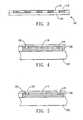
- First material layer 120is formed to fill in the space among the die 110 and adjacent dies 110 , and the surface of the first material layer 120 and the surface of the die 110 are at same level.
- the material of the first material layer 120can be UV curing type or heating curing type material. Then, the first material layer 120 is cured by UV or thermal.
- the first material layer 120may be formed by a screen printing method or a photolithography method.
- the first material layer 120functions as a buffer layer to reduce a stress due to temperature, etc.
- the first material layer 120can be a UV and/or heat curing material, such as silicon rubber, epoxy, resin, BCB, and so on.
- the aforementioned structure 102comprising the base 100 , the dies 110 , and the first material layer 120 , looks same as a wafer with the dies 110 facing above.
- a second material layer 122is coated on the structure 102 .
- the material of the second material layer 120can be UV curing type or heating curing type material, such as BCB, epoxy, SINR3170 (produced by Shin-Etsu Chemical Co.,Ltd.), and so on.
- the partial area of the second material layer 122 on the pads 116 of the die 110is removed by using a photo mask to form first openings 124 on the pads 116 , and then the second material layer 120 is cured by UV or heating.
- the plasma etching (RIE)can be used optionally to clean the surface of the pads 116 to make sure no residual materials on the pads 116 .
- the contact conductive layer 126is formed on the pads 116 , as shown in FIG. 6 .
- the preferable material of the contact conductive layer 126is Ti, Cu, or the combination thereof.
- the contact conductive layer 126can be formed by a physical method, a chemical method, or the combination thereof, for example: CVD, PVD, sputter, and electroplating.
- a photo resist layer 128is formed on the second material layer 122 and the contact conductive layer 126 , and then a fan out pattern of the photo resist layer 128 is developed by using a photo mask.
- the fan out patternhas a plurality of fan out openings starting form the pads 116 to end points inside a surface of the second dielectric layer 122 , respectively.
- the end points of two adjacent fan out openingscan have wider pitches there between than the pitch between two adjacent pads 116 .
- conductive lines 130 by electro platingare formed on the contact conductive layer 126 , as shown in FIG. 7 (vertical view) and FIG. 8 (lateral view, along a-a′ in FIG. 7 ).
- the material of the conductive lines 130are preferably Cu, Ni, Au, or the combination thereof.
- the photo resist layer 128 and the contact conductive layer 126are etched, and then an isolation layer 132 is formed on the conductive lines 130 and the second material layer 122 , and the second openings 134 are formed on the conductive lines 130 by using a photo mask.
- the first isolation layer 132is cured.
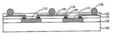
- the first isolation layer 132may be formed by spin coating or screen printing.
- the positions of the second openings 134may be formed above the die 110 or the first material layer 120 , preferably formed close to the ending points of the conductive lines 130 respectively, so a suitable distance between two adjacent second openings 134 is to form solder balls 136 on second openings 134 without the problem of signal coupling and signal interface.
- an epoxy layer 140is formed on the back side of the base 100 , i.e. on the surface of the base 100 having no die 110 formed thereon. Then, a top mark is formed on the epoxy layer 140 by using a photo mask and the epoxy layer 140 is cured. Or using the ink printing with stencil then heat/UV curing to form a top mark. The top mark is for identified the device name. The step of forming the epoxy layer 140 may be omitted. Next, the solder balls 136 are placed onto the solder openings 134 and joined the solder balls 136 and the surface of the conductive lines 130 with IR re-flow.
- the packaged base 100 with the aforementioned structureis sawed along the sawing line 138 to isolate respective packaged IC.
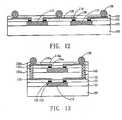
- the packaged ICmay be included passive component 142 and the die 110 , as shown in FIG. 11 .
- the packaged ICalso may be a multi dies with side by side structure, as shown in FIG. 12 .
- the package process of the present inventioneven can apply to form multi dies with stacking structure.
- die 110 ais placed on the isolation layer 132 in the vertical direction of the dies 110 .
- the third material layer 120 a , the fourth material layer 122 a , the second contact conductive layer 126 aare formed in sequence as aforementioned.
- Third openingsare formed by etching the third material layer 120 a , the fourth material layer 122 a , and the first isolation layer 132 .
- conductive material 148is placed into the third openings and the conductive material 148 is coupled with the conductive lines 130 .
- the conductive material 148may be a solder.
- a second conductive lines 130 a , a second isolation layer 132 a , and solder balls 136are formed in sequence.
- the material of the third material layer 120 a and the fourth material layer 122 acan be UV curing type or heating curing type material;
- the preferable material of the second contact conductive layer 126 ais Ti, Cu, or the combination thereof;
- the material of the second conductive lines 130 aare preferably Cu, Ni, Au, or the combination thereof.
- FIG. 13only shows a stacking package structure with two dies, it is obvious that a stacking package structure with more than two dies can be obtained as aforementioned.
- the aforementioned package structurecan maintain an appropriate pitch between two adjacent solder balls of the package structure. Therefore, the present invention can avoid the problems of signal coupling and signal interface. Moreover, the present invention also employs a glass substrate for LCD and the size of the glass substrate is very larger, so the present invention can lower the cost of the package structure and raise the yield of the package structure. Moreover, the package size of the present invention can be easily adjusted to test equipment, package equipment, etc.
Landscapes
- Engineering & Computer Science (AREA)
- Microelectronics & Electronic Packaging (AREA)
- Power Engineering (AREA)
- Computer Hardware Design (AREA)
- General Physics & Mathematics (AREA)
- Condensed Matter Physics & Semiconductors (AREA)
- Physics & Mathematics (AREA)
- Manufacturing & Machinery (AREA)
- Wire Bonding (AREA)
- Micromachines (AREA)
- Piezo-Electric Or Mechanical Vibrators, Or Delay Or Filter Circuits (AREA)
- Structures Or Materials For Encapsulating Or Coating Semiconductor Devices Or Solid State Devices (AREA)
- Solid State Image Pick-Up Elements (AREA)
- Internal Circuitry In Semiconductor Integrated Circuit Devices (AREA)
- Electric Connection Of Electric Components To Printed Circuits (AREA)
Abstract
Description
- 1. Field of the Invention
- This invention relates to a package for semiconductors, and more particularly to a fan out type wafer level package.
- 2. Description of the Prior Art
- The semiconductor technologies are developing very fast, and especially semiconductor dies have a tendency toward miniaturization. However, the requirements for the functions of the semiconductor dies have an opposite tendency to variety. Namely, the semiconductor dies must have more I/O pads into a smaller area, so the density of the pins is raised quickly. It causes the packaging for the semiconductor dies to become more difficult and decrease the yield.
- The main purpose of the package structure is to protect the dies from outside damages. Furthermore, the heat generated by the dies must be diffused efficiently through the package structure to ensure the operation the dies.
- The earlier lead frame package technology is already not suitable for the advanced semiconductor dies due to the density of the pins thereof is too high. Hence, a new package technology of BGA (Ball Grid Array) has been developed to satisfy the packaging requirement for the advanced semiconductor dies. The BGA package has an advantage of that the spherical pins has a shorter pitch than that of the lead frame package and the pins is hard to damage and deform. In addition, the shorter signal transmitting distance benefits to raise the operating frequency to conform to the requirement of faster efficiency. For example, the U.S. Pat. No. 5,629,835 discloses a BGA package, by Mahulikar et al; the U.S. Pat. No. 5,239,198 discloses another package that the FR4 substrates having a pattern of conductive traces thereon are mounted on a PCB; the Taiwan patent No.177,766 discloses a fan out type WLP, by the inventor of the present invention.
- Most of the package technologies divide dies on a wafer into respective dies and then to package and test the die respectively.
- Another package technology, called “Wafer Level Package (WLP)”, can package the dies on a wafer before dividing the dies into respective dies.
- The WLP technology has some advantages, such as a shorter producing cycle time, lower cost, and no need to under-fill or molding.
- The U.S. Pat. No. 5,323,051, “Semiconductor wafer level package”, is disclosed a WLP technology by Adams et al. The technology is described as follow. As shown in
FIG. 1 , a die4 is formed on a surface of a semiconductor wafer2, and a cap wafer6 with a predetermined pattern of frit glass walls8 as a bonding agent is deposited on a surface of the semiconductor wafer2, such that the die4 is completely surrounded by the frit glass walls8. Then, a surface of the semiconductor wafer2 without the die4 is polished to reduce the height of the semiconductor wafer2; the process is generally called “Back Grinding”. The die4 is hermetically sealed in a cavity of predetermined dimensions formed by a combination of the semiconductor wafer2, the cap wafer6, and the frit glass walls8. A plurality ofmetal traces 10 forms a plurality of electrodes on semiconductor substrate wafer2 which provide electrical coupling to die4. A plurality ofwires 12 is bonded to a plurality of pads formed on exterior portions ofmetal traces 10, and extends throughhole 14 and is coupled to external electrical dies (not shown). - 7
- As aforementioned, the size of the die is very small, and the I/O pads are formed on a surface of a die in the conventional arts. Therefore, number of the pads is limited and a too short pitch among pads results in a problem of signal coupling or signal interface. The solder is also to form a solder bridge easily due to the too short pitch among pads. Moreover, the size of die gradually become smaller and the packaged IC of the die does not have standard size by some package technologies (such as chip size package), but test equipment, package equipment, etc. for some fixed sizes die or packages can not be kept on using.
- Therefore, the present invention has been made in view of the above problems in the prior arts, and it is an objective of the present invention to provide a fan out type wafer level package structure and a method for manufacturing the same.
- Another objective of the present invention is to provide a fan out type wafer level package structure to maintain an appropriate pitch between two adjacent pads of the package structure.
- Still another objective of the present invention is to avoid problems of signal coupling and signal interface.
- Another objective of the present invention is to lower the cost of the package structure.
- Still another objective of the present invention is to raise the yield of the package structure.
- Another objective of the present invention is to provide package structure with a adjustable size to keep on using of test equipment, package equipment, etc. having for some fixed sizes die or packages.
- As aforementioned, the present invention provides a process of fan out type wafer level package. First, a plurality of dies is adhered to an isolating base. A first material layer is formed on the isolating base, wherein a space among the plurality of dies on the isolating base is filled up with the first material layer, and surfaces of the first material layer and the plurality of dies are at same level. Then, the first material layer is cured. A second material layer is formed on the first material layer and the plurality of dies. A partial region of the second material layer on pads of the plurality of dies is etched to form first openings. Next, the second material layer is cured. Contact conductive layer are formed on the first openings to electrically coupling with the pads, respectively. A photo resist layer is formed on the second material layer and the contact conductive layer. A partial region of the photo resist layer is removed to form a fan out pattern and expose the contact conductive layer. After that, conductive lines are formed on the fan out pattern and the conductive lines are coupled with the contact conductive layer, respectively. The remaining photo resist layer is removed. Following that, an isolation layer is formed on the conductive lines and the second material layer. A partial region of the isolation layer on the conductive lines is removed to forming second openings. The isolation layer is cured. Finally, solder balls are welded on the second openings and the base is sawed to isolate the plurality of dies. The present invention also provides a fan out type package structure. The package structure comprises an isolating base, a die, a first dielectric layer, a second dielectric layer, a contact conductive layer, conductive lines, an isolation layer, and solder balls. The die is adhered to the isolating base. The first dielectric layer is formed on the isolating base and filled in a space except the die on the isolating base, wherein surfaces of the first dielectric layer and the die are at same level. The second dielectric layer is formed on the first dielectric layer and the die, and the second dielectric layer has first openings on pads of the die. The contact conductive layer is formed on the first openings to electrically coupling with the pads, respectively. The conductive lines are formed on the second dielectric layer and corresponding the contact conductive layer, and the conductive lines are extended out from corresponding the contact conductive layer to corresponding end points, wherein the corresponding end points are inside a surface of the second dielectric layer. The isolation layer is formed on the conductive lines and the second dielectric layer, and the isolation layer has second openings on the conductive lines. The solder balls are welded on the second openings and electrical coupling with the conductive lines, respectively.
FIG. 1 is a schematic diagram of a semiconductor wafer level package in the conventional arts;FIG. 2A toFIG. 2C are schematic diagrams of using pick & place to replace standard dies onto a new base;FIG. 3 is a schematic diagram of forming a first material layer on the base;FIG. 4 is a schematic diagram of forming a second material layer on the first material layer and the die;FIG. 5 is a schematic diagram of etching a partial region of the second material layer on pads of the die to form first openings;FIG. 6 is a schematic diagram of forming contact conductive layer on the first openings;FIG. 7 is a schematic vertical view diagram of forming conductive lines on fan out pattern formed by a photo resist layer;FIG. 8 is a schematic lateral view diagram of forming conductive lines on fan out pattern formed by a photo resist layer along a-a′ inFIG. 7 ;FIG. 9 is a schematic diagram of forming an isolation layer on the conductive lines and the second material layer;FIG. 10 is a schematic diagram of one packaged structure according to the present invention;FIG. 11 is a schematic diagram of one packaged structure having a die and a passive component according to the present invention;FIG. 12 is a schematic diagram of one packaged structure having two dies according to the present invention; andFIG. 13 is a schematic diagram of one packaged stacking structure having two dies according to the present invention- Some sample embodiments of the invention will now be described in greater detail. Nevertheless, it should be recognized that the present invention can be practiced in a wide range of other embodiments besides those explicitly described, and the scope of the present invention is expressly not limited expect as specified in the accompanying claims.
- Then, the components of the different elements are not shown to scale. Some dimensions of the related components are exaggerated and meaningless portions are not drawn to provide a more clear description and comprehension of the present invention.
- The essence of the present invention is to pick and place standard dies on a new base for obtaining an appropriate and wider distance between dies than the original distance of dies on a wafer. Therefore, the package structure has a larger size of balls array than the size of the die to avoid the problem of having too close ball pitch. Moreover, the die may be packaged with passive components (ex. capacitors) or other dies with a side by side structure or a stacking structure. The detailed process of the present invention will be described below.
- A processed silicon wafer with dies is put on a tray and then the thickness of the processed silicon wafer is decreased by back lapping to get a thickness range of 50-300 μm. The processed silicon wafer with the aforementioned thickness is easily sawed to divide the dies on the wafer into respective dies. The back lapping step may be omitted if the processed silicon wafer is not hard to saw without back lapping. A dielectric layer (protection layer) is optionally formed on the processed silicon wafer before sawing to protect dies form damages.
- The divided dies are tested to choose standard good dies110 there from. The standard good dies110 are picked and replaced onto a
new base 100 with a wider distance between two adjacent dies and adhered to the base100 with an UV curing type and/or heat curing type adhesion material with good thermal conductivity (not shown), as shown inFIG. 2A . The adhesion material is coating on thebase 100, and the thickness of the adhesion material is preferably 20-60 μm. When the dies110 are placed on the adhesion material, the adhesion material is cured by UV light or thermal. The distance between two adjacent dies on thebase 100 is arranged wider to have enough space for forming fan out ball array in later steps. Hence, the present invention can maintain an ideal ball pitch for avoiding problems of signal coupling and signal interface and increase the number of I/O ports (balls), even the size of dies becomes smaller. The dies110 have I/O pads 116 on the upper surface (as shown inFIG. 4 ).Passive components 114 or dies112 are also placed on an adjacent place of the base100 to obtain a filtering or other functions, as shown inFIG. 2B andFIG. 2C . The material of the base100 can be glass, silicon, ceramic, crystal materials, etc. and even have a round or a rectangular shape. In the present invention, the number of dies and passive components packaged together are not limited. More than three dies and passive components also can be packaged in the same package structure by the present invention. The adhesive material of the present invention is preferably good thermal conductive material, so the problems (such as stress) resulted from the temperature difference between the dies110 and the base100 can be avoided. - The illustration and the corresponding figure below are made through single die to simplify and provide a more clear description comprehension of the present invention.
First material layer 120 is formed to fill in the space among thedie 110 and adjacent dies110, and the surface of thefirst material layer 120 and the surface of thedie 110 are at same level. The material of thefirst material layer 120 can be UV curing type or heating curing type material. Then, thefirst material layer 120 is cured by UV or thermal. Thefirst material layer 120 may be formed by a screen printing method or a photolithography method. Thefirst material layer 120 functions as a buffer layer to reduce a stress due to temperature, etc. Thefirst material layer 120 can be a UV and/or heat curing material, such as silicon rubber, epoxy, resin, BCB, and so on. Theaforementioned structure 102, comprising thebase 100, the dies110, and thefirst material layer 120, looks same as a wafer with the dies110 facing above.- As shown in
FIG. 4 , asecond material layer 122 is coated on thestructure 102. The material of thesecond material layer 120 can be UV curing type or heating curing type material, such as BCB, epoxy, SINR3170 (produced by Shin-Etsu Chemical Co.,Ltd.), and so on. Then, the partial area of thesecond material layer 122 on thepads 116 of thedie 110 is removed by using a photo mask to formfirst openings 124 on thepads 116, and then thesecond material layer 120 is cured by UV or heating. Next, the plasma etching (RIE) can be used optionally to clean the surface of thepads 116 to make sure no residual materials on thepads 116. - The contact
conductive layer 126 is formed on thepads 116, as shown inFIG. 6 . The preferable material of the contactconductive layer 126 is Ti, Cu, or the combination thereof. The contactconductive layer 126 can be formed by a physical method, a chemical method, or the combination thereof, for example: CVD, PVD, sputter, and electroplating. A photo resistlayer 128 is formed on thesecond material layer 122 and the contactconductive layer 126, and then a fan out pattern of the photo resistlayer 128 is developed by using a photo mask. The fan out pattern has a plurality of fan out openings starting form thepads 116 to end points inside a surface of thesecond dielectric layer 122, respectively. Namely, the end points of two adjacent fan out openings can have wider pitches there between than the pitch between twoadjacent pads 116. Then,conductive lines 130 by electro plating are formed on the contactconductive layer 126, as shown inFIG. 7 (vertical view) andFIG. 8 (lateral view, along a-a′ inFIG. 7 ). The material of theconductive lines 130 are preferably Cu, Ni, Au, or the combination thereof. - Referring to
FIG. 9 , the photo resistlayer 128 and the contactconductive layer 126 are etched, and then anisolation layer 132 is formed on theconductive lines 130 and thesecond material layer 122, and the second openings134 are formed on theconductive lines 130 by using a photo mask. Next, thefirst isolation layer 132 is cured. Thefirst isolation layer 132 may be formed by spin coating or screen printing. The positions of the second openings134 may be formed above thedie 110 or thefirst material layer 120, preferably formed close to the ending points of theconductive lines 130 respectively, so a suitable distance between two adjacent second openings134 is to formsolder balls 136 on second openings134 without the problem of signal coupling and signal interface. - Referring to
FIG. 10 , anepoxy layer 140 is formed on the back side of thebase 100, i.e. on the surface of the base100 having no die110 formed thereon. Then, a top mark is formed on theepoxy layer 140 by using a photo mask and theepoxy layer 140 is cured. Or using the ink printing with stencil then heat/UV curing to form a top mark. The top mark is for identified the device name. The step of forming theepoxy layer 140 may be omitted. Next, thesolder balls 136 are placed onto the solder openings134 and joined thesolder balls 136 and the surface of theconductive lines 130 with IR re-flow. - Final, the packaged
base 100 with the aforementioned structure is sawed along thesawing line 138 to isolate respective packaged IC. As aforementioned, the packaged IC may be includedpassive component 142 and thedie 110, as shown inFIG. 11 . The packaged IC also may be a multi dies with side by side structure, as shown inFIG. 12 . - The package process of the present invention even can apply to form multi dies with stacking structure. Referring to
FIG. 13 , after the step of forming theisolation layer 132 or the second openings134, die110ais placed on theisolation layer 132 in the vertical direction of the dies110. Then, thethird material layer 120a, thefourth material layer 122a, the second contactconductive layer 126aare formed in sequence as aforementioned. Third openings are formed by etching thethird material layer 120a, thefourth material layer 122a, and thefirst isolation layer 132. Thenconductive material 148 is placed into the third openings and theconductive material 148 is coupled with theconductive lines 130. Theconductive material 148 may be a solder. Next, similar to the above illustrations ofFIG. 7 toFIG. 10 , a secondconductive lines 130a, asecond isolation layer 132a, andsolder balls 136 are formed in sequence. Similarly, the material of thethird material layer 120aand thefourth material layer 122acan be UV curing type or heating curing type material; the preferable material of the second contactconductive layer 126ais Ti, Cu, or the combination thereof; the material of the secondconductive lines 130aare preferably Cu, Ni, Au, or the combination thereof. AlthoughFIG. 13 only shows a stacking package structure with two dies, it is obvious that a stacking package structure with more than two dies can be obtained as aforementioned. - Hence, according to the present invention, the aforementioned package structure can maintain an appropriate pitch between two adjacent solder balls of the package structure. Therefore, the present invention can avoid the problems of signal coupling and signal interface. Moreover, the present invention also employs a glass substrate for LCD and the size of the glass substrate is very larger, so the present invention can lower the cost of the package structure and raise the yield of the package structure. Moreover, the package size of the present invention can be easily adjusted to test equipment, package equipment, etc.
- Although specific embodiments have been illustrated and described, it will be obvious to those skilled in the art that various modifications may be made without departing from what is intended to be limited solely by the appended claims.
Claims (47)
Priority Applications (13)
| Application Number | Priority Date | Filing Date | Title |
|---|---|---|---|
| US10/725,933US7459781B2 (en) | 2003-12-03 | 2003-12-03 | Fan out type wafer level package structure and method of the same |
| TW093109319ATWI244742B (en) | 2003-12-03 | 2004-04-02 | Fan out type wafer level package structure and method of the same |
| CNB2004100432707ACN1324667C (en) | 2003-12-03 | 2004-05-20 | Structure and Formation Method of Diffused Wafer Type Package |
| SG200402998ASG114665A1 (en) | 2003-12-03 | 2004-05-25 | Fan out type wafer level package structure and method of the same |
| KR1020040044013AKR100824160B1 (en) | 2003-12-03 | 2004-06-15 | Open wafer level package structure and manufacturing method thereof |
| DE102004033057ADE102004033057A1 (en) | 2003-12-03 | 2004-07-08 | Fan-out type wafer level package structure and method for making the same |
| JP2004220573AJP2005167191A (en) | 2003-12-03 | 2004-07-28 | Fan-out wafer level package structure and manufacturing method thereof |
| US11/169,722US7262081B2 (en) | 2003-12-03 | 2005-06-30 | Fan out type wafer level package structure and method of the same |
| US11/301,303US7196408B2 (en) | 2003-12-03 | 2005-12-12 | Fan out type wafer level package structure and method of the same |
| US11/456,141US7514767B2 (en) | 2003-12-03 | 2006-07-07 | Fan out type wafer level package structure and method of the same |
| US11/595,970US20070059866A1 (en) | 2003-12-03 | 2006-11-13 | Fan out type wafer level package structure and method of the same |
| US11/946,424US7557437B2 (en) | 2003-12-03 | 2007-11-28 | Fan out type wafer level package structure and method of the same |
| US12/255,868US7667318B2 (en) | 2003-12-03 | 2008-10-22 | Fan out type wafer level package structure and method of the same |
Applications Claiming Priority (1)
| Application Number | Priority Date | Filing Date | Title |
|---|---|---|---|
| US10/725,933US7459781B2 (en) | 2003-12-03 | 2003-12-03 | Fan out type wafer level package structure and method of the same |
Related Child Applications (5)
| Application Number | Title | Priority Date | Filing Date |
|---|---|---|---|
| US11/169,722DivisionUS7262081B2 (en) | 2003-12-03 | 2005-06-30 | Fan out type wafer level package structure and method of the same |
| US11/301,303DivisionUS7196408B2 (en) | 2003-12-03 | 2005-12-12 | Fan out type wafer level package structure and method of the same |
| US11/456,141Continuation-In-PartUS7514767B2 (en) | 2003-12-03 | 2006-07-07 | Fan out type wafer level package structure and method of the same |
| US11/946,424ContinuationUS7557437B2 (en) | 2003-12-03 | 2007-11-28 | Fan out type wafer level package structure and method of the same |
| US12/255,868DivisionUS7667318B2 (en) | 2003-12-03 | 2008-10-22 | Fan out type wafer level package structure and method of the same |
Publications (2)
| Publication Number | Publication Date |
|---|---|
| US20050124093A1true US20050124093A1 (en) | 2005-06-09 |
| US7459781B2 US7459781B2 (en) | 2008-12-02 |
Family
ID=34633314
Family Applications (6)
| Application Number | Title | Priority Date | Filing Date |
|---|---|---|---|
| US10/725,933Expired - LifetimeUS7459781B2 (en) | 2003-12-03 | 2003-12-03 | Fan out type wafer level package structure and method of the same |
| US11/169,722Expired - LifetimeUS7262081B2 (en) | 2003-12-03 | 2005-06-30 | Fan out type wafer level package structure and method of the same |
| US11/301,303Expired - LifetimeUS7196408B2 (en) | 2003-12-03 | 2005-12-12 | Fan out type wafer level package structure and method of the same |
| US11/595,970AbandonedUS20070059866A1 (en) | 2003-12-03 | 2006-11-13 | Fan out type wafer level package structure and method of the same |
| US11/946,424Expired - LifetimeUS7557437B2 (en) | 2003-12-03 | 2007-11-28 | Fan out type wafer level package structure and method of the same |
| US12/255,868Expired - LifetimeUS7667318B2 (en) | 2003-12-03 | 2008-10-22 | Fan out type wafer level package structure and method of the same |
Family Applications After (5)
| Application Number | Title | Priority Date | Filing Date |
|---|---|---|---|
| US11/169,722Expired - LifetimeUS7262081B2 (en) | 2003-12-03 | 2005-06-30 | Fan out type wafer level package structure and method of the same |
| US11/301,303Expired - LifetimeUS7196408B2 (en) | 2003-12-03 | 2005-12-12 | Fan out type wafer level package structure and method of the same |
| US11/595,970AbandonedUS20070059866A1 (en) | 2003-12-03 | 2006-11-13 | Fan out type wafer level package structure and method of the same |
| US11/946,424Expired - LifetimeUS7557437B2 (en) | 2003-12-03 | 2007-11-28 | Fan out type wafer level package structure and method of the same |
| US12/255,868Expired - LifetimeUS7667318B2 (en) | 2003-12-03 | 2008-10-22 | Fan out type wafer level package structure and method of the same |
Country Status (7)
| Country | Link |
|---|---|
| US (6) | US7459781B2 (en) |
| JP (1) | JP2005167191A (en) |
| KR (1) | KR100824160B1 (en) |
| CN (1) | CN1324667C (en) |
| DE (1) | DE102004033057A1 (en) |
| SG (1) | SG114665A1 (en) |
| TW (1) | TWI244742B (en) |
Cited By (34)
| Publication number | Priority date | Publication date | Assignee | Title |
|---|---|---|---|---|
| US20060240664A1 (en)* | 2005-04-01 | 2006-10-26 | Kenji Wada | Method of manufacturing multi-layered substrate |
| US20070052895A1 (en)* | 2005-09-05 | 2007-03-08 | Wan-Jung Chen | Fan-out wire structure |
| US20070249102A1 (en)* | 2006-04-21 | 2007-10-25 | Infineon Technologies Ag | Panel and semiconductor device having a structure with a low-k dielectric |
| US20080041616A1 (en)* | 2006-08-21 | 2008-02-21 | Tpo Displays Corp. | Layout of a printed circuit board |
| US20080135977A1 (en)* | 2006-12-07 | 2008-06-12 | Infineon Technologies Ag | Semiconductor component including a semiconductor chip and a passive component |
| US20080169539A1 (en)* | 2007-01-12 | 2008-07-17 | Silicon Storage Tech., Inc. | Under bump metallurgy structure of a package and method of making same |
| US20080258277A1 (en)* | 2007-04-19 | 2008-10-23 | Infineon Technologies Ag | Semiconductor Device Comprising a Semiconductor Chip Stack and Method for Producing the Same |
| US20080303151A1 (en)* | 2007-06-08 | 2008-12-11 | Analog Devices, Inc. | Method of Packaging a Microchip |
| DE102008013180A1 (en) | 2007-03-08 | 2008-12-24 | Advanced Chip Engineering Technology Inc., Hukou | Structure of a semiconductor device package and its method |
| US20090072394A1 (en)* | 2007-02-28 | 2009-03-19 | Masanori Onodera | Semiconductor device and method of manufacturing the same |
| US20090230527A1 (en)* | 2008-03-13 | 2009-09-17 | Geng-Shin Shen | Multi-chips package structure and the method thereof |
| US20100084759A1 (en)* | 2007-12-20 | 2010-04-08 | Geng-Shin Shen | Die Rearrangement Package Structure Using Layout Process to Form a Compliant Configuration |
| US20100155916A1 (en)* | 2008-03-20 | 2010-06-24 | Geng-Shin Shen | Chip package structure and the method thereof with adhering the chips to a frame and forming ubm layers |
| US7977163B1 (en)* | 2005-12-08 | 2011-07-12 | Amkor Technology, Inc. | Embedded electronic component package fabrication method |
| US20110316117A1 (en)* | 2007-08-14 | 2011-12-29 | Agency For Science, Technology And Research | Die package and a method for manufacturing the die package |
| US8119455B1 (en) | 2002-11-08 | 2012-02-21 | Amkor Technology, Inc. | Wafer level package fabrication method |
| US8188584B1 (en) | 2002-11-08 | 2012-05-29 | Amkor Technology, Inc. | Direct-write wafer level chip scale package |
| US20120231582A1 (en)* | 2008-11-26 | 2012-09-13 | Infineon Technologies Ag | Device including a semiconductor chip |
| US20120287583A1 (en)* | 2007-06-13 | 2012-11-15 | Infineon Technologies Ag | Embedded chip package |
| CN103904057A (en)* | 2014-04-02 | 2014-07-02 | 华进半导体封装先导技术研发中心有限公司 | PoP structure and manufacturing technology |
| US8786110B2 (en) | 2010-09-24 | 2014-07-22 | J-Devices Corporation | Semiconductor device and manufacturing method thereof |
| US8822268B1 (en)* | 2013-07-17 | 2014-09-02 | Freescale Semiconductor, Inc. | Redistributed chip packages containing multiple components and methods for the fabrication thereof |
| US8901754B2 (en) | 2010-06-22 | 2014-12-02 | J-Devices Corporation | Semiconductor device and manufacturing method thereof |
| US9013017B2 (en) | 2012-10-15 | 2015-04-21 | Stmicroelectronics Pte Ltd | Method for making image sensors using wafer-level processing and associated devices |
| CN104681456A (en)* | 2015-01-27 | 2015-06-03 | 华进半导体封装先导技术研发中心有限公司 | Fan-out-type wafer level package method |
| US9059058B2 (en) | 2012-10-22 | 2015-06-16 | Stmicroelectronics Pte Ltd | Image sensor device with IR filter and related methods |
| US9343396B2 (en) | 2010-02-25 | 2016-05-17 | Stats Chippac, Ltd. | Semiconductor device and method of forming IPD in fan-out wafer level chip scale package |
| US20170271209A1 (en)* | 2011-10-11 | 2017-09-21 | Taiwan Semiconductor Manufacturing Company, Ltd. | Methods of Packaging Semiconductor Devices and Structures Thereof |
| EP3273476A1 (en)* | 2012-12-20 | 2018-01-24 | INTEL Corporation | High density organic bridge device and method |
| CN110875294A (en)* | 2018-08-29 | 2020-03-10 | 凤凰先驱股份有限公司 | Packaging structure of semiconductor device and manufacturing method thereof |
| US10971467B2 (en)* | 2016-01-22 | 2021-04-06 | Sj Semiconductor (Jiangyin) Corporation | Packaging method and package structure of fan-out chip |
| US11508695B2 (en)* | 2016-09-09 | 2022-11-22 | Taiwan Semiconductor Manufacturing Company, Ltd. | Redistribution layers in semiconductor packages and methods of forming same |
| US11652063B2 (en) | 2016-02-26 | 2023-05-16 | Taiwan Semiconductor Manufacturing Company, Ltd. | Semiconductor package and method of forming the same |
| US12174539B2 (en) | 2019-07-29 | 2024-12-24 | Asahi Kasei Kabushiki Kaisha | Negative photosensitive resin composition, production method for polyimide, production method for cured relief pattern, and semiconductor device |
Families Citing this family (141)
| Publication number | Priority date | Publication date | Assignee | Title |
|---|---|---|---|---|
| US7271489B2 (en)* | 2003-10-15 | 2007-09-18 | Megica Corporation | Post passivation interconnection schemes on top of the IC chips |
| US7579681B2 (en)* | 2002-06-11 | 2009-08-25 | Micron Technology, Inc. | Super high density module with integrated wafer level packages |
| JP2006041438A (en)* | 2004-07-30 | 2006-02-09 | Shinko Electric Ind Co Ltd | Semiconductor chip built-in substrate, and its manufacturing method |
| DE102004063994B4 (en)* | 2004-10-26 | 2009-01-02 | Advanced Chip Engineering Technology Inc. | Chip-sized packing structure |
| DE102004058413B4 (en)* | 2004-10-26 | 2006-10-19 | Advanced Chip Engineering Technology Inc. | Method for producing a chip-size packing structure |
| TWI263313B (en)* | 2005-08-15 | 2006-10-01 | Phoenix Prec Technology Corp | Stack structure of semiconductor component embedded in supporting board |
| US7902660B1 (en) | 2006-05-24 | 2011-03-08 | Amkor Technology, Inc. | Substrate for semiconductor device and manufacturing method thereof |
| CN100468934C (en)* | 2006-12-06 | 2009-03-11 | 威盛电子股份有限公司 | Voltage converter and method thereof |
| US20080197469A1 (en)* | 2007-02-21 | 2008-08-21 | Advanced Chip Engineering Technology Inc. | Multi-chips package with reduced structure and method for forming the same |
| US8304923B2 (en)* | 2007-03-29 | 2012-11-06 | ADL Engineering Inc. | Chip packaging structure |
| US7994622B2 (en) | 2007-04-16 | 2011-08-09 | Tessera, Inc. | Microelectronic packages having cavities for receiving microelectric elements |
| TWI353644B (en)* | 2007-04-25 | 2011-12-01 | Ind Tech Res Inst | Wafer level packaging structure |
| CA2687120A1 (en)* | 2007-05-08 | 2008-11-13 | Scanimetrics Inc. | Ultra high speed signal transmission/reception |
| JP2008306105A (en)* | 2007-06-11 | 2008-12-18 | Oki Electric Ind Co Ltd | Method for manufacturing semiconductor device |
| KR20090007120A (en)* | 2007-07-13 | 2009-01-16 | 삼성전자주식회사 | Wafer level laminated package to achieve redistribution through encapsulation and manufacturing method |
| US8759964B2 (en) | 2007-07-17 | 2014-06-24 | Taiwan Semiconductor Manufacturing Company, Ltd. | Wafer level package structure and fabrication methods |
| KR100885924B1 (en) | 2007-08-10 | 2009-02-26 | 삼성전자주식회사 | Semiconductor package including buried conductive posts and manufacturing method thereof |
| TWI339865B (en)* | 2007-08-17 | 2011-04-01 | Chipmos Technologies Inc | A dice rearrangement package method |
| TWI360207B (en) | 2007-10-22 | 2012-03-11 | Advanced Semiconductor Eng | Chip package structure and method of manufacturing |
| CN101436552B (en)* | 2007-11-16 | 2010-12-08 | 南茂科技股份有限公司 | Manufacturing method using net structure in package structure with reconfigured crystal grains |
| CN101436553B (en)* | 2007-11-16 | 2010-06-02 | 南茂科技股份有限公司 | Manufacturing method using metal bump in chip reconfiguration packaging structure |
| DE102007061161A1 (en)* | 2007-12-17 | 2009-06-18 | Advanced Chip Engineering Technology Inc. | Electronic packing structure e.g. electronic three dimensional package, for manufacturing e.g. micro electronic, signal contact formed on side of structure connected with contact to form canal between contact and inner switching circuit |
| TWI364801B (en)* | 2007-12-20 | 2012-05-21 | Chipmos Technologies Inc | Dice rearrangement package structure using layout process to form a compliant configuration |
| CN101477955B (en)* | 2008-01-04 | 2013-04-10 | 南茂科技股份有限公司 | Small chip reconfiguration packaging structure and packaging method |
| CN101477956B (en)* | 2008-01-04 | 2012-05-16 | 南茂科技股份有限公司 | Small chip reconfiguration packaging structure and packaging method |
| CN101488462B (en)* | 2008-01-15 | 2010-12-08 | 南茂科技股份有限公司 | Modular multi-die package structure and method thereof |
| JP4504434B2 (en)* | 2008-02-14 | 2010-07-14 | 株式会社東芝 | Integrated semiconductor device |
| US20090230554A1 (en)* | 2008-03-13 | 2009-09-17 | Broadcom Corporation | Wafer-level redistribution packaging with die-containing openings |
| US20090236647A1 (en)* | 2008-03-18 | 2009-09-24 | Infineon Technologies Ag | Semiconductor device with capacitor |
| KR101501739B1 (en) | 2008-03-21 | 2015-03-11 | 삼성전자주식회사 | Method of Fabricating Semiconductor Packages |
| CN101567322B (en)* | 2008-04-21 | 2010-11-17 | 南茂科技股份有限公司 | Chip packaging structure and packaging method thereof |
| US8318540B2 (en)* | 2008-05-19 | 2012-11-27 | Infineon Technologies Ag | Method of manufacturing a semiconductor structure |
| TWI387014B (en)* | 2008-06-05 | 2013-02-21 | Chipmos Technologies Inc | Die reconfiguration structure with sacrificial substrate and packaging method thereof |
| TWI387074B (en)* | 2008-06-05 | 2013-02-21 | Chipmos Technologies Inc | Grain stack structure and forming method thereof |
| TWI387077B (en)* | 2008-06-12 | 2013-02-21 | Chipmos Technologies Inc | Grain reconfigurable package structure and method thereof |
| CN101615584B (en)* | 2008-06-25 | 2011-06-15 | 南茂科技股份有限公司 | Packaging method for chip reconfiguration |
| CN101615583B (en)* | 2008-06-25 | 2011-05-18 | 南茂科技股份有限公司 | Formation method of chip stack structure |
| CN101621041B (en)* | 2008-07-02 | 2011-03-23 | 南茂科技股份有限公司 | Package structure and method for chip reconfiguration |
| TWI453877B (en)* | 2008-11-07 | 2014-09-21 | Advanced Semiconductor Eng | Structure and process of embedded chip package |
| US7863096B2 (en)* | 2008-07-17 | 2011-01-04 | Fairchild Semiconductor Corporation | Embedded die package and process flow using a pre-molded carrier |
| US9164404B2 (en) | 2008-09-19 | 2015-10-20 | Intel Corporation | System and process for fabricating semiconductor packages |
| US9165841B2 (en) | 2008-09-19 | 2015-10-20 | Intel Corporation | System and process for fabricating semiconductor packages |
| KR100999531B1 (en)* | 2008-10-20 | 2010-12-08 | 삼성전기주식회사 | Printed circuit board and manufacturing method thereof |
| US8354304B2 (en)* | 2008-12-05 | 2013-01-15 | Stats Chippac, Ltd. | Semiconductor device and method of forming conductive posts embedded in photosensitive encapsulant |
| US20100167471A1 (en) | 2008-12-30 | 2010-07-01 | Stmicroelectronics Asia Pacific Pte. Ltd. | Reducing warpage for fan-out wafer level packaging |
| JP2010219489A (en)* | 2009-02-20 | 2010-09-30 | Toshiba Corp | Semiconductor device and manufacturing method thereof |
| FR2946795B1 (en)* | 2009-06-12 | 2011-07-22 | 3D Plus | METHOD FOR POSITIONING CHIPS WHEN MANUFACTURING A RECONSTITUTED PLATE |
| TWI456715B (en)* | 2009-06-19 | 2014-10-11 | Advanced Semiconductor Eng | Chip package structure and manufacturing method thereof |
| CN101604638B (en)* | 2009-06-26 | 2010-10-06 | 江阴长电先进封装有限公司 | Wafer level fan-out chip packaging method |
| TWI466259B (en)* | 2009-07-21 | 2014-12-21 | Advanced Semiconductor Eng | Semiconductor package, manufacturing method thereof and manufacturing method for chip-redistribution encapsulant |
| TWI405306B (en)* | 2009-07-23 | 2013-08-11 | Advanced Semiconductor Eng | Semiconductor package, manufacturing method thereof and chip-redistribution encapsulant |
| US8003496B2 (en)* | 2009-08-14 | 2011-08-23 | Stats Chippac, Ltd. | Semiconductor device and method of mounting semiconductor die to heat spreader on temporary carrier and forming polymer layer and conductive layer over the die |
| TWI528514B (en)* | 2009-08-20 | 2016-04-01 | 精材科技股份有限公司 | Chip package and fabrication method thereof |
| TWI501376B (en)* | 2009-10-07 | 2015-09-21 | Xintec Inc | Chip package and fabrication method thereof |
| US20110084372A1 (en) | 2009-10-14 | 2011-04-14 | Advanced Semiconductor Engineering, Inc. | Package carrier, semiconductor package, and process for fabricating same |
| US8378466B2 (en)* | 2009-11-19 | 2013-02-19 | Advanced Semiconductor Engineering, Inc. | Wafer-level semiconductor device packages with electromagnetic interference shielding |
| TWI497679B (en)* | 2009-11-27 | 2015-08-21 | Advanced Semiconductor Eng | Semiconductor package and manufacturing method thereof |
| US8435837B2 (en) | 2009-12-15 | 2013-05-07 | Silicon Storage Technology, Inc. | Panel based lead frame packaging method and device |
| US20110156239A1 (en)* | 2009-12-29 | 2011-06-30 | Stmicroelectronics Asia Pacific Pte Ltd. | Method for manufacturing a fan-out embedded panel level package |
| US8569894B2 (en) | 2010-01-13 | 2013-10-29 | Advanced Semiconductor Engineering, Inc. | Semiconductor package with single sided substrate design and manufacturing methods thereof |
| US8372689B2 (en)* | 2010-01-21 | 2013-02-12 | Advanced Semiconductor Engineering, Inc. | Wafer-level semiconductor device packages with three-dimensional fan-out and manufacturing methods thereof |
| US8320134B2 (en)* | 2010-02-05 | 2012-11-27 | Advanced Semiconductor Engineering, Inc. | Embedded component substrate and manufacturing methods thereof |
| JP5232185B2 (en)* | 2010-03-05 | 2013-07-10 | 株式会社東芝 | Manufacturing method of semiconductor device |
| US8409926B2 (en) | 2010-03-09 | 2013-04-02 | Stats Chippac, Ltd. | Semiconductor device and method of forming insulating layer around semiconductor die |
| TWI411075B (en)* | 2010-03-22 | 2013-10-01 | Advanced Semiconductor Eng | Semiconductor package and manufacturing method thereof |
| US8278746B2 (en) | 2010-04-02 | 2012-10-02 | Advanced Semiconductor Engineering, Inc. | Semiconductor device packages including connecting elements |
| US8624374B2 (en) | 2010-04-02 | 2014-01-07 | Advanced Semiconductor Engineering, Inc. | Semiconductor device packages with fan-out and with connecting elements for stacking and manufacturing methods thereof |
| CN102237330B (en)* | 2010-05-07 | 2015-08-05 | 三星电子株式会社 | Wafer-class encapsulation |
| CN102254834B (en)* | 2010-05-18 | 2016-04-27 | 异基因开发有限责任公司 | Semiconductor package and method |
| JP2012009545A (en)* | 2010-06-23 | 2012-01-12 | Toshiba Corp | Semiconductor device manufacturing method |
| US8343810B2 (en) | 2010-08-16 | 2013-01-01 | Stats Chippac, Ltd. | Semiconductor device and method of forming Fo-WLCSP having conductive layers and conductive vias separated by polymer layers |
| US8502367B2 (en) | 2010-09-29 | 2013-08-06 | Stmicroelectronics Pte Ltd. | Wafer-level packaging method using composite material as a base |
| DE102010046963A1 (en)* | 2010-09-29 | 2012-03-29 | Infineon Technologies Ag | Multi-Chip Package |
| TWI501365B (en)* | 2010-10-13 | 2015-09-21 | Ind Tech Res Inst | Package unit, stacking structure thereof and manufacturing method thereof |
| US8941222B2 (en) | 2010-11-11 | 2015-01-27 | Advanced Semiconductor Engineering Inc. | Wafer level semiconductor package and manufacturing methods thereof |
| US9406658B2 (en) | 2010-12-17 | 2016-08-02 | Advanced Semiconductor Engineering, Inc. | Embedded component device and manufacturing methods thereof |
| KR101195463B1 (en)* | 2011-02-15 | 2012-10-30 | 에스케이하이닉스 주식회사 | Semiconductor package and method for forming the same |
| US9721872B1 (en) | 2011-02-18 | 2017-08-01 | Amkor Technology, Inc. | Methods and structures for increasing the allowable die size in TMV packages |
| US8487426B2 (en) | 2011-03-15 | 2013-07-16 | Advanced Semiconductor Engineering, Inc. | Semiconductor package with embedded die and manufacturing methods thereof |
| US9595490B2 (en)* | 2011-03-22 | 2017-03-14 | Nantong Fujitsu Microelectronics Co., Ltd. | 3D system-level packaging methods and structures |
| WO2012126377A1 (en) | 2011-03-22 | 2012-09-27 | Nantong Fujitsu Microelectronics Co., Ltd. | System-level packaging methods and structures |
| US8597986B2 (en)* | 2011-09-01 | 2013-12-03 | Taiwan Semiconductor Manufacturing Co., Ltd. | System in package and method of fabricating same |
| US8698297B2 (en)* | 2011-09-23 | 2014-04-15 | Stats Chippac Ltd. | Integrated circuit packaging system with stack device |
| US8664756B2 (en)* | 2012-07-24 | 2014-03-04 | Medtronic, Inc. | Reconstituted wafer package with high voltage discrete active dice and integrated field plate for high temperature leakage current stability |
| EP2761653B1 (en) | 2011-09-30 | 2016-05-04 | Medtronic Inc. | Reconstituted wafer package with a discrete high voltage dice and integrated field plate for high temperature leakage current stability |
| US8649820B2 (en) | 2011-11-07 | 2014-02-11 | Blackberry Limited | Universal integrated circuit card apparatus and related methods |
| KR101831938B1 (en) | 2011-12-09 | 2018-02-23 | 삼성전자주식회사 | Method of fabricating fan-out wafer level pacakge and the package formed by the method |
| US9691706B2 (en)* | 2012-01-23 | 2017-06-27 | Taiwan Semiconductor Manufacturing Company, Ltd. | Multi-chip fan out package and methods of forming the same |
| US9111949B2 (en)* | 2012-04-09 | 2015-08-18 | Taiwan Semiconductor Manufacturing Company, Ltd. | Methods and apparatus of wafer level package for heterogeneous integration technology |
| USD703208S1 (en) | 2012-04-13 | 2014-04-22 | Blackberry Limited | UICC apparatus |
| US8936199B2 (en) | 2012-04-13 | 2015-01-20 | Blackberry Limited | UICC apparatus and related methods |
| USD701864S1 (en) | 2012-04-23 | 2014-04-01 | Blackberry Limited | UICC apparatus |
| DE112012006409T5 (en)* | 2012-05-23 | 2015-02-26 | Intel Corporation | A multi-stack package BBUL |
| US9345813B2 (en)* | 2012-06-07 | 2016-05-24 | Medos International S.A.R.L. | Three dimensional packaging for medical implants |
| KR101452587B1 (en)* | 2012-06-28 | 2014-10-22 | 타이완 세미콘덕터 매뉴팩쳐링 컴퍼니 리미티드 | Methods and apparatus of wafer level package for heterogeneous integration technology |
| KR101429344B1 (en) | 2012-08-08 | 2014-08-12 | 앰코 테크놀로지 코리아 주식회사 | Semiconductor Package and Manufacturing Methode thereof |
| CN103681610B (en)* | 2012-09-04 | 2017-05-10 | 旺宏电子股份有限公司 | Chip stack structure and manufacturing method thereof |
| TWI552663B (en)* | 2012-09-07 | 2016-10-01 | 環旭電子股份有限公司 | A system with circuit board and manufacturing method thereof |
| CN103681381B (en)* | 2012-09-07 | 2016-07-06 | 环旭电子股份有限公司 | Circuit board systems and manufacture method thereof |
| US9520323B2 (en)* | 2012-09-11 | 2016-12-13 | Freescale Semiconductor, Inc. | Microelectronic packages having trench vias and methods for the manufacture thereof |
| KR101999262B1 (en) | 2012-09-12 | 2019-07-12 | 삼성전자주식회사 | Semiconductor Package and method for fabricating the same |
| KR20140038116A (en)* | 2012-09-20 | 2014-03-28 | 제이앤제이 패밀리 주식회사 | Led lamp |
| US10157876B2 (en) | 2012-10-19 | 2018-12-18 | Taiwan Semiconductor Manufacturing Company Limited | Method of forming inductor with conductive trace |
| US9761553B2 (en) | 2012-10-19 | 2017-09-12 | Taiwan Semiconductor Manufacturing Company Limited | Inductor with conductive trace |
| US9799592B2 (en) | 2013-11-19 | 2017-10-24 | Amkor Technology, Inc. | Semicondutor device with through-silicon via-less deep wells |
| KR101366461B1 (en) | 2012-11-20 | 2014-02-26 | 앰코 테크놀로지 코리아 주식회사 | Semiconductor device and manufacturing method thereof |
| US9431369B2 (en)* | 2012-12-13 | 2016-08-30 | Taiwan Semiconductor Manufacturing Company, Ltd. | Antenna apparatus and method |
| US9455160B2 (en)* | 2013-01-14 | 2016-09-27 | Infineon Technologies Ag | Method for fabricating a semiconductor chip panel |
| US9685350B2 (en)* | 2013-03-08 | 2017-06-20 | STATS ChipPAC, Pte. Ltd. | Semiconductor device and method of forming embedded conductive layer for power/ground planes in Fo-eWLB |
| KR101488590B1 (en) | 2013-03-29 | 2015-01-30 | 앰코 테크놀로지 코리아 주식회사 | Semiconductor device and manufacturing method thereof |
| DE102013107862A1 (en)* | 2013-07-23 | 2015-01-29 | Osram Opto Semiconductors Gmbh | Surface-mountable optoelectronic semiconductor component and method for producing at least one surface-mountable optoelectronic semiconductor component |
| JP2015056458A (en)* | 2013-09-10 | 2015-03-23 | 株式会社東芝 | Semiconductor device |
| KR101607981B1 (en) | 2013-11-04 | 2016-03-31 | 앰코 테크놀로지 코리아 주식회사 | Interposer and method for manufacturing the same, and semiconductor package using the same |
| CN103904056A (en)* | 2014-04-02 | 2014-07-02 | 华进半导体封装先导技术研发中心有限公司 | PoP packaging structure and manufacturing technology |
| CN104157619B (en)* | 2014-08-22 | 2016-09-28 | 山东华芯半导体有限公司 | A kind of novel PoP stack package structure and manufacture method thereof |
| TWI581690B (en)* | 2014-12-30 | 2017-05-01 | 恆勁科技股份有限公司 | Package apparatus and manufacturing method thereof |
| CN104795380A (en)* | 2015-03-27 | 2015-07-22 | 江阴长电先进封装有限公司 | Three-dimensional packaging structure |
| CN106298726A (en)* | 2015-05-27 | 2017-01-04 | 佳邦科技股份有限公司 | Semiconductor packaging structure and semiconductor packaging method |
| US9779940B2 (en)* | 2015-07-01 | 2017-10-03 | Zhuahai Advanced Chip Carriers & Electronic Substrate Solutions Technologies Co. Ltd. | Chip package |
| US9735131B2 (en)* | 2015-11-10 | 2017-08-15 | Taiwan Semiconductor Manufacturing Company, Ltd. | Multi-stack package-on-package structures |
| KR102420125B1 (en) | 2015-12-10 | 2022-07-13 | 삼성전자주식회사 | Semiconductor package and method of fabricating the same |
| KR102049255B1 (en)* | 2016-06-20 | 2019-11-28 | 삼성전자주식회사 | Fan-out semiconductor package |
| US10269732B2 (en)* | 2016-07-20 | 2019-04-23 | Taiwan Semiconductor Manufacturing Company, Ltd. | Info package with integrated antennas or inductors |
| US10332841B2 (en) | 2016-07-20 | 2019-06-25 | Taiwan Semiconductor Manufacturing Company, Ltd. | System on integrated chips and methods of forming the same |
| US9960328B2 (en) | 2016-09-06 | 2018-05-01 | Amkor Technology, Inc. | Semiconductor device and manufacturing method thereof |
| JP2018142611A (en) | 2017-02-27 | 2018-09-13 | 信越化学工業株式会社 | Manufacturing method for semiconductor device |
| US10923417B2 (en) | 2017-04-26 | 2021-02-16 | Taiwan Semiconductor Manufacturing Company Limited | Integrated fan-out package with 3D magnetic core inductor |
| US20180374717A1 (en)* | 2017-06-23 | 2018-12-27 | Powertech Technology Inc. | Semiconductor package and method of forming the same |
| CN112011149A (en)* | 2019-06-01 | 2020-12-01 | 南京航空航天大学 | A kind of high dielectric quasicrystal composite material substrate and preparation method thereof |
| CN112349601A (en)* | 2019-08-09 | 2021-02-09 | 矽磐微电子(重庆)有限公司 | Manufacturing method of chip packaging structure |
| CN112349595A (en)* | 2019-08-09 | 2021-02-09 | 矽磐微电子(重庆)有限公司 | Manufacturing method of chip packaging structure |
| CN115039029A (en) | 2020-01-30 | 2022-09-09 | 旭化成株式会社 | Negative photosensitive resin composition and method for producing cured relief pattern |
| US11482480B2 (en)* | 2020-03-19 | 2022-10-25 | Advanced Semiconductor Engineering, Inc. | Package substrate including an optically-cured dielecetric layer and method for manufacturing the package substrate |
| US11791281B2 (en) | 2020-03-19 | 2023-10-17 | Advanced Semiconductor Engineering, Inc. | Package substrate and method for manufacturing the same |
| TWI817316B (en) | 2021-01-12 | 2023-10-01 | 日商旭化成股份有限公司 | Polyimide precursor resin composition and manufacturing method thereof |
| WO2022158358A1 (en) | 2021-01-22 | 2022-07-28 | 旭化成株式会社 | Photosensitive resin composition, production method for polyimide cured film using same, and polyimide cured film |
| KR20230113814A (en) | 2021-01-22 | 2023-08-01 | 아사히 가세이 가부시키가이샤 | Photosensitive resin composition, method for producing a polyimide cured film using the same, and polyimide cured film |
| KR20220132070A (en) | 2021-03-22 | 2022-09-30 | 삼성전자주식회사 | semiconductor package |
| TWI870812B (en) | 2022-05-23 | 2025-01-21 | 日商旭化成股份有限公司 | Photosensitive resin composition, method for producing polyimide cured film using the same, and polyimide cured film |
| CN115101427A (en)* | 2022-08-26 | 2022-09-23 | 成都奕斯伟系统集成电路有限公司 | Manufacturing method of chip packaging structure and chip packaging structure |
| JP7462089B1 (en)* | 2023-03-13 | 2024-04-04 | 株式会社フジクラ | Semiconductor package and phased array antenna module |
Citations (7)
| Publication number | Priority date | Publication date | Assignee | Title |
|---|---|---|---|---|
| US5745984A (en)* | 1995-07-10 | 1998-05-05 | Martin Marietta Corporation | Method for making an electronic module |
| US5841193A (en)* | 1996-05-20 | 1998-11-24 | Epic Technologies, Inc. | Single chip modules, repairable multichip modules, and methods of fabrication thereof |
| US6271469B1 (en)* | 1999-11-12 | 2001-08-07 | Intel Corporation | Direct build-up layer on an encapsulated die package |
| US6417025B1 (en)* | 2001-04-02 | 2002-07-09 | Alien Technology Corporation | Integrated circuit packages assembled utilizing fluidic self-assembly |
| US6423570B1 (en)* | 2000-10-18 | 2002-07-23 | Intel Corporation | Method to protect an encapsulated die package during back grinding with a solder metallization layer and devices formed thereby |
| US20030122243A1 (en)* | 2001-12-31 | 2003-07-03 | Jin-Yuan Lee | Integrated chip package structure using organic substrate and method of manufacturing the same |
| US6888240B2 (en)* | 2001-04-30 | 2005-05-03 | Intel Corporation | High performance, low cost microelectronic circuit package with interposer |
Family Cites Families (42)
| Publication number | Priority date | Publication date | Assignee | Title |
|---|---|---|---|---|
| US153194A (en)* | 1874-07-21 | Improvement in respiring apparatus | ||
| US118501A (en)* | 1871-08-29 | Improvement in machines for undermining coal | ||
| JPH0834264B2 (en)* | 1987-04-21 | 1996-03-29 | 住友電気工業株式会社 | Semiconductor device and manufacturing method thereof |
| US5200362A (en) | 1989-09-06 | 1993-04-06 | Motorola, Inc. | Method of attaching conductive traces to an encapsulated semiconductor die using a removable transfer film |
| US5323051A (en) | 1991-12-16 | 1994-06-21 | Motorola, Inc. | Semiconductor wafer level package |
| US5353498A (en) | 1993-02-08 | 1994-10-11 | General Electric Company | Method for fabricating an integrated circuit module |
| US5629835A (en) | 1994-07-19 | 1997-05-13 | Olin Corporation | Metal ball grid array package with improved thermal conductivity |
| US5808360A (en)* | 1996-05-15 | 1998-09-15 | Micron Technology, Inc. | Microbump interconnect for bore semiconductor dice |
| KR100452661B1 (en)* | 1999-02-03 | 2004-10-14 | 가부시끼가이샤 도시바 | Method of dividing wafers and manufacturing semiconductor devices |
| JP2000275693A (en) | 1999-03-20 | 2000-10-06 | Natl Space Development Agency Of Japan | Optical function element |
| US6288905B1 (en)* | 1999-04-15 | 2001-09-11 | Amerasia International Technology Inc. | Contact module, as for a smart card, and method for making same |
| KR100319624B1 (en)* | 1999-05-20 | 2002-01-09 | 김영환 | Semiconductor chip package and method for fabricating thereof |
| US6154366A (en)* | 1999-11-23 | 2000-11-28 | Intel Corporation | Structures and processes for fabricating moisture resistant chip-on-flex packages |
| US6396148B1 (en)* | 2000-02-10 | 2002-05-28 | Epic Technologies, Inc. | Electroless metal connection structures and methods |
| US6555908B1 (en)* | 2000-02-10 | 2003-04-29 | Epic Technologies, Inc. | Compliant, solderable input/output bump structures |
| KR100344833B1 (en)* | 2000-04-03 | 2002-07-20 | 주식회사 하이닉스반도체 | Package of semiconductor and method for fabricating the same |
| JP2001320015A (en)* | 2000-05-12 | 2001-11-16 | Sony Corp | Semiconductor device and its manufacturing method |
| US6734534B1 (en)* | 2000-08-16 | 2004-05-11 | Intel Corporation | Microelectronic substrate with integrated devices |
| JP2002076196A (en)* | 2000-08-25 | 2002-03-15 | Nec Kansai Ltd | Chip type semiconductor device and manufacturing method thereof |
| DE10164800B4 (en)* | 2001-11-02 | 2005-03-31 | Infineon Technologies Ag | Method for producing an electronic component with a plurality of chips stacked on top of one another and contacted with one another |
| KR100435813B1 (en) | 2001-12-06 | 2004-06-12 | 삼성전자주식회사 | Multi chip package using metal bar and manufacturing method thereof |
| TW517361B (en)* | 2001-12-31 | 2003-01-11 | Megic Corp | Chip package structure and its manufacture process |
| US6673698B1 (en)* | 2002-01-19 | 2004-01-06 | Megic Corporation | Thin film semiconductor package utilizing a glass substrate with composite polymer/metal interconnect layers |
| TW503496B (en)* | 2001-12-31 | 2002-09-21 | Megic Corp | Chip packaging structure and manufacturing process of the same |
| CN1230897C (en)* | 2002-01-10 | 2005-12-07 | 育霈科技股份有限公司 | Semiconductor package structure and manufacturing method thereof |
| US6709897B2 (en)* | 2002-01-15 | 2004-03-23 | Unimicron Technology Corp. | Method of forming IC package having upward-facing chip cavity |
| TW557521B (en)* | 2002-01-16 | 2003-10-11 | Via Tech Inc | Integrated circuit package and its manufacturing process |
| CN1181525C (en)* | 2002-01-17 | 2004-12-22 | 裕沛科技股份有限公司 | Wafer type diffusion type packaging system |
| US6680529B2 (en) | 2002-02-15 | 2004-01-20 | Advanced Semiconductor Engineering, Inc. | Semiconductor build-up package |
| CN1215541C (en)* | 2002-03-20 | 2005-08-17 | 育霈科技股份有限公司 | Chip type package and manufacturing method thereof |
| TW543125B (en) | 2002-05-15 | 2003-07-21 | Advanced Chip Eng Tech Inc | Fan-out type wafer level package and the method of the same |
| TWI234253B (en) | 2002-05-31 | 2005-06-11 | Fujitsu Ltd | Semiconductor device and manufacturing method thereof |
| US6770971B2 (en)* | 2002-06-14 | 2004-08-03 | Casio Computer Co., Ltd. | Semiconductor device and method of fabricating the same |
| JP2004140037A (en) | 2002-10-15 | 2004-05-13 | Oki Electric Ind Co Ltd | Semiconductor device and its manufacturing process |
| TWI221327B (en) | 2003-08-08 | 2004-09-21 | Via Tech Inc | Multi-chip package and process for forming the same |
| TWI225670B (en) | 2003-12-09 | 2004-12-21 | Advanced Semiconductor Eng | Packaging method of multi-chip module |
| JP4204989B2 (en) | 2004-01-30 | 2009-01-07 | 新光電気工業株式会社 | Semiconductor device and manufacturing method thereof |
| US7208344B2 (en)* | 2004-03-31 | 2007-04-24 | Aptos Corporation | Wafer level mounting frame for ball grid array packaging, and method of making and using the same |
| JP2005332896A (en) | 2004-05-19 | 2005-12-02 | Oki Electric Ind Co Ltd | Semiconductor device, manufacturing method thereof, chip size package, and manufacturing method thereof |
| US7041576B2 (en) | 2004-05-28 | 2006-05-09 | Freescale Semiconductor, Inc. | Separately strained N-channel and P-channel transistors |
| DE102004041888B4 (en) | 2004-08-30 | 2007-03-08 | Infineon Technologies Ag | A manufacturing method of semiconductor device with stacked semiconductor devices |
| JP2006173232A (en) | 2004-12-14 | 2006-06-29 | Casio Comput Co Ltd | Semiconductor device and manufacturing method thereof |
- 2003
- 2003-12-03USUS10/725,933patent/US7459781B2/ennot_activeExpired - Lifetime
- 2004
- 2004-04-02TWTW093109319Apatent/TWI244742B/ennot_activeIP Right Cessation
- 2004-05-20CNCNB2004100432707Apatent/CN1324667C/ennot_activeExpired - Lifetime
- 2004-05-25SGSG200402998Apatent/SG114665A1/enunknown
- 2004-06-15KRKR1020040044013Apatent/KR100824160B1/ennot_activeExpired - Lifetime
- 2004-07-08DEDE102004033057Apatent/DE102004033057A1/ennot_activeWithdrawn
- 2004-07-28JPJP2004220573Apatent/JP2005167191A/enactivePending
- 2005
- 2005-06-30USUS11/169,722patent/US7262081B2/ennot_activeExpired - Lifetime
- 2005-12-12USUS11/301,303patent/US7196408B2/ennot_activeExpired - Lifetime
- 2006
- 2006-11-13USUS11/595,970patent/US20070059866A1/ennot_activeAbandoned
- 2007
- 2007-11-28USUS11/946,424patent/US7557437B2/ennot_activeExpired - Lifetime
- 2008
- 2008-10-22USUS12/255,868patent/US7667318B2/ennot_activeExpired - Lifetime
Patent Citations (7)
| Publication number | Priority date | Publication date | Assignee | Title |
|---|---|---|---|---|
| US5745984A (en)* | 1995-07-10 | 1998-05-05 | Martin Marietta Corporation | Method for making an electronic module |
| US5841193A (en)* | 1996-05-20 | 1998-11-24 | Epic Technologies, Inc. | Single chip modules, repairable multichip modules, and methods of fabrication thereof |
| US6271469B1 (en)* | 1999-11-12 | 2001-08-07 | Intel Corporation | Direct build-up layer on an encapsulated die package |
| US6423570B1 (en)* | 2000-10-18 | 2002-07-23 | Intel Corporation | Method to protect an encapsulated die package during back grinding with a solder metallization layer and devices formed thereby |
| US6417025B1 (en)* | 2001-04-02 | 2002-07-09 | Alien Technology Corporation | Integrated circuit packages assembled utilizing fluidic self-assembly |
| US6888240B2 (en)* | 2001-04-30 | 2005-05-03 | Intel Corporation | High performance, low cost microelectronic circuit package with interposer |
| US20030122243A1 (en)* | 2001-12-31 | 2003-07-03 | Jin-Yuan Lee | Integrated chip package structure using organic substrate and method of manufacturing the same |
Cited By (57)
| Publication number | Priority date | Publication date | Assignee | Title |
|---|---|---|---|---|
| US8691632B1 (en) | 2002-11-08 | 2014-04-08 | Amkor Technology, Inc. | Wafer level package and fabrication method |
| US9054117B1 (en) | 2002-11-08 | 2015-06-09 | Amkor Technology, Inc. | Wafer level package and fabrication method |
| US8188584B1 (en) | 2002-11-08 | 2012-05-29 | Amkor Technology, Inc. | Direct-write wafer level chip scale package |
| US8298866B1 (en) | 2002-11-08 | 2012-10-30 | Amkor Technology, Inc. | Wafer level package and fabrication method |
| US8486764B1 (en) | 2002-11-08 | 2013-07-16 | Amkor Technology, Inc. | Wafer level package and fabrication method |
| US8501543B1 (en) | 2002-11-08 | 2013-08-06 | Amkor Technology, Inc. | Direct-write wafer level chip scale package |
| US10665567B1 (en) | 2002-11-08 | 2020-05-26 | Amkor Technology, Inc. | Wafer level package and fabrication method |
| US8119455B1 (en) | 2002-11-08 | 2012-02-21 | Amkor Technology, Inc. | Wafer level package fabrication method |
| US9871015B1 (en) | 2002-11-08 | 2018-01-16 | Amkor Technology, Inc. | Wafer level package and fabrication method |
| US8952522B1 (en) | 2002-11-08 | 2015-02-10 | Amkor Technology, Inc. | Wafer level package and fabrication method |
| US8710649B1 (en) | 2002-11-08 | 2014-04-29 | Amkor Technology, Inc. | Wafer level package and fabrication method |
| US9406645B1 (en) | 2002-11-08 | 2016-08-02 | Amkor Technology, Inc. | Wafer level package and fabrication method |
| US20060240664A1 (en)* | 2005-04-01 | 2006-10-26 | Kenji Wada | Method of manufacturing multi-layered substrate |
| US20070052895A1 (en)* | 2005-09-05 | 2007-03-08 | Wan-Jung Chen | Fan-out wire structure |
| US7459780B2 (en)* | 2005-09-05 | 2008-12-02 | Au Optronics Corporation | Fan-out wire structure |
| US7977163B1 (en)* | 2005-12-08 | 2011-07-12 | Amkor Technology, Inc. | Embedded electronic component package fabrication method |
| US20070249102A1 (en)* | 2006-04-21 | 2007-10-25 | Infineon Technologies Ag | Panel and semiconductor device having a structure with a low-k dielectric |
| US7615706B2 (en)* | 2006-08-21 | 2009-11-10 | Tpo Displays Corp. | Layout of a printed circuit board |
| US20080041616A1 (en)* | 2006-08-21 | 2008-02-21 | Tpo Displays Corp. | Layout of a printed circuit board |
| US20080135977A1 (en)* | 2006-12-07 | 2008-06-12 | Infineon Technologies Ag | Semiconductor component including a semiconductor chip and a passive component |
| US8471393B2 (en) | 2006-12-07 | 2013-06-25 | Infineon Technologies Ag | Semiconductor component including a semiconductor chip and a passive component |
| US20080169539A1 (en)* | 2007-01-12 | 2008-07-17 | Silicon Storage Tech., Inc. | Under bump metallurgy structure of a package and method of making same |
| US9508651B2 (en)* | 2007-02-28 | 2016-11-29 | Cypress Semiconductor Corporation | Semiconductor device and method of manufacturing the same |
| US20090072394A1 (en)* | 2007-02-28 | 2009-03-19 | Masanori Onodera | Semiconductor device and method of manufacturing the same |
| US11018105B2 (en) | 2007-02-28 | 2021-05-25 | Cypress Semiconductor Corporation | Semiconductor device and method of manufacturing the same |
| DE102008013180A1 (en) | 2007-03-08 | 2008-12-24 | Advanced Chip Engineering Technology Inc., Hukou | Structure of a semiconductor device package and its method |
| US20080258277A1 (en)* | 2007-04-19 | 2008-10-23 | Infineon Technologies Ag | Semiconductor Device Comprising a Semiconductor Chip Stack and Method for Producing the Same |
| US7880285B2 (en) | 2007-04-19 | 2011-02-01 | Infineon Technologies Ag | Semiconductor device comprising a semiconductor chip stack and method for producing the same |
| US20080303151A1 (en)* | 2007-06-08 | 2008-12-11 | Analog Devices, Inc. | Method of Packaging a Microchip |
| US7749810B2 (en) | 2007-06-08 | 2010-07-06 | Analog Devices, Inc. | Method of packaging a microchip having a footprint that is larger than that of the integrated circuit |
| WO2008150564A1 (en)* | 2007-06-08 | 2008-12-11 | Analog Devices, Inc. | Method of packaging a microchip |
| US20120287583A1 (en)* | 2007-06-13 | 2012-11-15 | Infineon Technologies Ag | Embedded chip package |
| US20110316117A1 (en)* | 2007-08-14 | 2011-12-29 | Agency For Science, Technology And Research | Die package and a method for manufacturing the die package |
| US20100084759A1 (en)* | 2007-12-20 | 2010-04-08 | Geng-Shin Shen | Die Rearrangement Package Structure Using Layout Process to Form a Compliant Configuration |
| US7915690B2 (en)* | 2007-12-20 | 2011-03-29 | Chipmos Technologies Inc | Die rearrangement package structure using layout process to form a compliant configuration |
| US20090230527A1 (en)* | 2008-03-13 | 2009-09-17 | Geng-Shin Shen | Multi-chips package structure and the method thereof |
| US7888783B2 (en)* | 2008-03-20 | 2011-02-15 | Chipmos Technologies Inc | Chip package structure and the method thereof with adhering the chips to a frame and forming UBM layers |
| US20100155916A1 (en)* | 2008-03-20 | 2010-06-24 | Geng-Shin Shen | Chip package structure and the method thereof with adhering the chips to a frame and forming ubm layers |
| US20120231582A1 (en)* | 2008-11-26 | 2012-09-13 | Infineon Technologies Ag | Device including a semiconductor chip |
| US9343396B2 (en) | 2010-02-25 | 2016-05-17 | Stats Chippac, Ltd. | Semiconductor device and method of forming IPD in fan-out wafer level chip scale package |
| US8901754B2 (en) | 2010-06-22 | 2014-12-02 | J-Devices Corporation | Semiconductor device and manufacturing method thereof |
| US8786110B2 (en) | 2010-09-24 | 2014-07-22 | J-Devices Corporation | Semiconductor device and manufacturing method thereof |
| US20170271209A1 (en)* | 2011-10-11 | 2017-09-21 | Taiwan Semiconductor Manufacturing Company, Ltd. | Methods of Packaging Semiconductor Devices and Structures Thereof |
| US10163711B2 (en)* | 2011-10-11 | 2018-12-25 | Taiwan Semiconductor Manufacturing Company | Methods of packaging semiconductor devices including placing semiconductor devices into die caves |
| US10964594B2 (en) | 2011-10-11 | 2021-03-30 | Taiwan Semiconductor Manufacturing Company. | Methods of packaging semiconductor devices including placing semiconductor devices into die caves |
| US9013017B2 (en) | 2012-10-15 | 2015-04-21 | Stmicroelectronics Pte Ltd | Method for making image sensors using wafer-level processing and associated devices |
| US9059058B2 (en) | 2012-10-22 | 2015-06-16 | Stmicroelectronics Pte Ltd | Image sensor device with IR filter and related methods |
| EP3273476A1 (en)* | 2012-12-20 | 2018-01-24 | INTEL Corporation | High density organic bridge device and method |
| US12002762B2 (en) | 2012-12-20 | 2024-06-04 | Intel Corporation | High density organic bridge device and method |
| US8822268B1 (en)* | 2013-07-17 | 2014-09-02 | Freescale Semiconductor, Inc. | Redistributed chip packages containing multiple components and methods for the fabrication thereof |
| CN103904057A (en)* | 2014-04-02 | 2014-07-02 | 华进半导体封装先导技术研发中心有限公司 | PoP structure and manufacturing technology |
| CN104681456A (en)* | 2015-01-27 | 2015-06-03 | 华进半导体封装先导技术研发中心有限公司 | Fan-out-type wafer level package method |
| US10971467B2 (en)* | 2016-01-22 | 2021-04-06 | Sj Semiconductor (Jiangyin) Corporation | Packaging method and package structure of fan-out chip |
| US11652063B2 (en) | 2016-02-26 | 2023-05-16 | Taiwan Semiconductor Manufacturing Company, Ltd. | Semiconductor package and method of forming the same |
| US11508695B2 (en)* | 2016-09-09 | 2022-11-22 | Taiwan Semiconductor Manufacturing Company, Ltd. | Redistribution layers in semiconductor packages and methods of forming same |
| CN110875294A (en)* | 2018-08-29 | 2020-03-10 | 凤凰先驱股份有限公司 | Packaging structure of semiconductor device and manufacturing method thereof |
| US12174539B2 (en) | 2019-07-29 | 2024-12-24 | Asahi Kasei Kabushiki Kaisha | Negative photosensitive resin composition, production method for polyimide, production method for cured relief pattern, and semiconductor device |
Also Published As
| Publication number | Publication date |
|---|---|
| JP2005167191A (en) | 2005-06-23 |
| SG114665A1 (en) | 2005-09-28 |
| US7557437B2 (en) | 2009-07-07 |
| US20090051025A1 (en) | 2009-02-26 |
| US20060091514A1 (en) | 2006-05-04 |
| KR20050053476A (en) | 2005-06-08 |
| US7196408B2 (en) | 2007-03-27 |
| US7262081B2 (en) | 2007-08-28 |
| US7459781B2 (en) | 2008-12-02 |
| US20080105967A1 (en) | 2008-05-08 |
| CN1624888A (en) | 2005-06-08 |
| CN1324667C (en) | 2007-07-04 |
| TWI244742B (en) | 2005-12-01 |
| US20050236696A1 (en) | 2005-10-27 |
| DE102004033057A1 (en) | 2005-06-30 |
| US20070059866A1 (en) | 2007-03-15 |
| US7667318B2 (en) | 2010-02-23 |
| KR100824160B1 (en) | 2008-04-21 |
| TW200520190A (en) | 2005-06-16 |
Similar Documents
| Publication | Publication Date | Title |
|---|---|---|
| US7262081B2 (en) | Fan out type wafer level package structure and method of the same | |
| US7514767B2 (en) | Fan out type wafer level package structure and method of the same | |
| US7339279B2 (en) | Chip-size package structure and method of the same | |
| US7061106B2 (en) | Structure of image sensor module and a method for manufacturing of wafer level package | |
| US7413925B2 (en) | Method for fabricating semiconductor package | |
| CN1147928C (en) | Semiconductor device having sub-chip-scale package structure and method for forming same | |
| US6528344B2 (en) | Chip scale surface-mountable packaging method for electronic and MEMS devices | |
| JP4472682B2 (en) | Manufacturing method of wafer level chip scale package of image sensor | |
| US7498646B2 (en) | Structure of image sensor module and a method for manufacturing of wafer level package | |
| US20080083980A1 (en) | Cmos image sensor chip scale package with die receiving through-hole and method of the same | |
| US20080191335A1 (en) | Cmos image sensor chip scale package with die receiving opening and method of the same | |
| US20080217761A1 (en) | Structure of semiconductor device package and method of the same | |
| JP2008244437A (en) | Image sensor package with die receiving opening and method thereof | |
| KR20020091327A (en) | Wafer level package having a package body at its side surface and method for manufacturing the same | |
| CN101252108A (en) | Semiconductor device package having die receiving via and connecting via and method thereof | |
| US20090321903A1 (en) | Semiconductor device and manufacturing method thereof | |
| JP3394696B2 (en) | Semiconductor device and manufacturing method thereof | |
| JP2004006670A (en) | Semiconductor wafer with spacer and method of manufacturing the same, semiconductor device and method of manufacturing the same, circuit board, and electronic equipment |
Legal Events
| Date | Code | Title | Description |
|---|---|---|---|
| AS | Assignment | Owner name:ADVANCED CHIP ENGINEERING TECHNOLOGY INC., TAIWAN Free format text:ASSIGNMENT OF ASSIGNORS INTEREST;ASSIGNORS:YANG, WEN-KUN;YANG, WEN-PIN;CHEN, SHIH-LI;REEL/FRAME:014279/0151;SIGNING DATES FROM 20031208 TO 20031212 | |
| AS | Assignment | Owner name:WEN-KUN YANG, TAIWAN Free format text:ASSIGNMENT OF ASSIGNORS INTEREST;ASSIGNOR:ADVANCED CHIP ENGINEERING TECHNOLOGY INC.;REEL/FRAME:014362/0508 Effective date:20040210 | |
| STCF | Information on status: patent grant | Free format text:PATENTED CASE | |
| AS | Assignment | Owner name:ADVANCED CHIP ENGINEERING TECHNOLOGY INC., TAIWAN Free format text:LEGAL DOCUMENTS LISTED ON APPENDIX A;ASSIGNOR:YANG, WEN-KUN;REEL/FRAME:022086/0001 Effective date:20031203 | |
| AS | Assignment | Owner name:ADVANCED CHIP ENGINEERING TECHNOLOGY INC., TAIWAN Free format text:ASSIGNMENT OF ASSIGNORS INTEREST;ASSIGNOR:YANG, WEN-KUN;REEL/FRAME:022868/0528 Effective date:20090625 Owner name:ADVANCED CHIP ENGINEERING TECHNOLOGY INC.,TAIWAN Free format text:ASSIGNMENT OF ASSIGNORS INTEREST;ASSIGNOR:YANG, WEN-KUN;REEL/FRAME:022868/0528 Effective date:20090625 | |
| FPAY | Fee payment | Year of fee payment:4 | |
| FPAY | Fee payment | Year of fee payment:8 | |
| MAFP | Maintenance fee payment | Free format text:PAYMENT OF MAINTENANCE FEE, 12TH YR, SMALL ENTITY (ORIGINAL EVENT CODE: M2553); ENTITY STATUS OF PATENT OWNER: SMALL ENTITY Year of fee payment:12 | |
| AS | Assignment | Owner name:ADL ENERGY CORP., TAIWAN Free format text:CHANGE OF NAME;ASSIGNOR:ADL ENGINEERING INC.;REEL/FRAME:064927/0462 Effective date:20220105 Owner name:ADL ENGINEERING INC., TAIWAN Free format text:MERGER;ASSIGNORS:ADL ENGINEERING INC.;ADVANCED CHIP ENGINEERING TECHNOLOGY INC.;REEL/FRAME:064926/0845 Effective date:20120613 | |
| AS | Assignment | Owner name:TAIWAN SEMICONDUCTOR MANUFACTURING COMPANY, LTD., TAIWAN Free format text:ASSIGNMENT OF ASSIGNORS INTEREST;ASSIGNOR:ADL ENERGY CORP.;REEL/FRAME:065957/0661 Effective date:20230914 |