US20050121764A1 - Stackable integrated circuit packaging - Google Patents
Stackable integrated circuit packagingDownload PDFInfo
- Publication number
- US20050121764A1 US20050121764A1US10/728,324US72832403AUS2005121764A1US 20050121764 A1US20050121764 A1US 20050121764A1US 72832403 AUS72832403 AUS 72832403AUS 2005121764 A1US2005121764 A1US 2005121764A1
- Authority
- US
- United States
- Prior art keywords
- integrated circuit
- die
- interconnect
- package
- contact
- Prior art date
- Legal status (The legal status is an assumption and is not a legal conclusion. Google has not performed a legal analysis and makes no representation as to the accuracy of the status listed.)
- Granted
Links
Images


Classifications
- H—ELECTRICITY
- H01—ELECTRIC ELEMENTS
- H01L—SEMICONDUCTOR DEVICES NOT COVERED BY CLASS H10
- H01L25/00—Assemblies consisting of a plurality of semiconductor or other solid state devices
- H01L25/03—Assemblies consisting of a plurality of semiconductor or other solid state devices all the devices being of a type provided for in a single subclass of subclasses H10B, H10D, H10F, H10H, H10K or H10N, e.g. assemblies of rectifier diodes
- H01L25/04—Assemblies consisting of a plurality of semiconductor or other solid state devices all the devices being of a type provided for in a single subclass of subclasses H10B, H10D, H10F, H10H, H10K or H10N, e.g. assemblies of rectifier diodes the devices not having separate containers
- H01L25/065—Assemblies consisting of a plurality of semiconductor or other solid state devices all the devices being of a type provided for in a single subclass of subclasses H10B, H10D, H10F, H10H, H10K or H10N, e.g. assemblies of rectifier diodes the devices not having separate containers the devices being of a type provided for in group H10D89/00
- H01L25/0657—Stacked arrangements of devices
- H—ELECTRICITY
- H01—ELECTRIC ELEMENTS
- H01L—SEMICONDUCTOR DEVICES NOT COVERED BY CLASS H10
- H01L23/00—Details of semiconductor or other solid state devices
- H01L23/48—Arrangements for conducting electric current to or from the solid state body in operation, e.g. leads, terminal arrangements ; Selection of materials therefor
- H01L23/488—Arrangements for conducting electric current to or from the solid state body in operation, e.g. leads, terminal arrangements ; Selection of materials therefor consisting of soldered or bonded constructions
- H01L23/498—Leads, i.e. metallisations or lead-frames on insulating substrates, e.g. chip carriers
- H01L23/49811—Additional leads joined to the metallisation on the insulating substrate, e.g. pins, bumps, wires, flat leads
- H01L23/49816—Spherical bumps on the substrate for external connection, e.g. ball grid arrays [BGA]
- H—ELECTRICITY
- H01—ELECTRIC ELEMENTS
- H01L—SEMICONDUCTOR DEVICES NOT COVERED BY CLASS H10
- H01L24/00—Arrangements for connecting or disconnecting semiconductor or solid-state bodies; Methods or apparatus related thereto
- H01L24/93—Batch processes
- H01L24/95—Batch processes at chip-level, i.e. with connecting carried out on a plurality of singulated devices, i.e. on diced chips
- H01L24/97—Batch processes at chip-level, i.e. with connecting carried out on a plurality of singulated devices, i.e. on diced chips the devices being connected to a common substrate, e.g. interposer, said common substrate being separable into individual assemblies after connecting
- H—ELECTRICITY
- H01—ELECTRIC ELEMENTS
- H01L—SEMICONDUCTOR DEVICES NOT COVERED BY CLASS H10
- H01L25/00—Assemblies consisting of a plurality of semiconductor or other solid state devices
- H01L25/03—Assemblies consisting of a plurality of semiconductor or other solid state devices all the devices being of a type provided for in a single subclass of subclasses H10B, H10D, H10F, H10H, H10K or H10N, e.g. assemblies of rectifier diodes
- H01L25/10—Assemblies consisting of a plurality of semiconductor or other solid state devices all the devices being of a type provided for in a single subclass of subclasses H10B, H10D, H10F, H10H, H10K or H10N, e.g. assemblies of rectifier diodes the devices having separate containers
- H01L25/105—Assemblies consisting of a plurality of semiconductor or other solid state devices all the devices being of a type provided for in a single subclass of subclasses H10B, H10D, H10F, H10H, H10K or H10N, e.g. assemblies of rectifier diodes the devices having separate containers the devices being integrated devices of class H10
- H—ELECTRICITY
- H01—ELECTRIC ELEMENTS
- H01L—SEMICONDUCTOR DEVICES NOT COVERED BY CLASS H10
- H01L2224/00—Indexing scheme for arrangements for connecting or disconnecting semiconductor or solid-state bodies and methods related thereto as covered by H01L24/00
- H01L2224/01—Means for bonding being attached to, or being formed on, the surface to be connected, e.g. chip-to-package, die-attach, "first-level" interconnects; Manufacturing methods related thereto
- H01L2224/26—Layer connectors, e.g. plate connectors, solder or adhesive layers; Manufacturing methods related thereto
- H01L2224/31—Structure, shape, material or disposition of the layer connectors after the connecting process
- H01L2224/32—Structure, shape, material or disposition of the layer connectors after the connecting process of an individual layer connector
- H01L2224/321—Disposition
- H01L2224/32135—Disposition the layer connector connecting between different semiconductor or solid-state bodies, i.e. chip-to-chip
- H01L2224/32145—Disposition the layer connector connecting between different semiconductor or solid-state bodies, i.e. chip-to-chip the bodies being stacked
- H—ELECTRICITY
- H01—ELECTRIC ELEMENTS
- H01L—SEMICONDUCTOR DEVICES NOT COVERED BY CLASS H10
- H01L2224/00—Indexing scheme for arrangements for connecting or disconnecting semiconductor or solid-state bodies and methods related thereto as covered by H01L24/00
- H01L2224/01—Means for bonding being attached to, or being formed on, the surface to be connected, e.g. chip-to-package, die-attach, "first-level" interconnects; Manufacturing methods related thereto
- H01L2224/26—Layer connectors, e.g. plate connectors, solder or adhesive layers; Manufacturing methods related thereto
- H01L2224/31—Structure, shape, material or disposition of the layer connectors after the connecting process
- H01L2224/32—Structure, shape, material or disposition of the layer connectors after the connecting process of an individual layer connector
- H01L2224/321—Disposition
- H01L2224/32151—Disposition the layer connector connecting between a semiconductor or solid-state body and an item not being a semiconductor or solid-state body, e.g. chip-to-substrate, chip-to-passive
- H01L2224/32221—Disposition the layer connector connecting between a semiconductor or solid-state body and an item not being a semiconductor or solid-state body, e.g. chip-to-substrate, chip-to-passive the body and the item being stacked
- H01L2224/32225—Disposition the layer connector connecting between a semiconductor or solid-state body and an item not being a semiconductor or solid-state body, e.g. chip-to-substrate, chip-to-passive the body and the item being stacked the item being non-metallic, e.g. insulating substrate with or without metallisation
- H—ELECTRICITY
- H01—ELECTRIC ELEMENTS
- H01L—SEMICONDUCTOR DEVICES NOT COVERED BY CLASS H10
- H01L2224/00—Indexing scheme for arrangements for connecting or disconnecting semiconductor or solid-state bodies and methods related thereto as covered by H01L24/00
- H01L2224/01—Means for bonding being attached to, or being formed on, the surface to be connected, e.g. chip-to-package, die-attach, "first-level" interconnects; Manufacturing methods related thereto
- H01L2224/42—Wire connectors; Manufacturing methods related thereto
- H01L2224/47—Structure, shape, material or disposition of the wire connectors after the connecting process
- H01L2224/48—Structure, shape, material or disposition of the wire connectors after the connecting process of an individual wire connector
- H01L2224/4805—Shape
- H01L2224/4809—Loop shape
- H01L2224/48091—Arched
- H—ELECTRICITY
- H01—ELECTRIC ELEMENTS
- H01L—SEMICONDUCTOR DEVICES NOT COVERED BY CLASS H10
- H01L2224/00—Indexing scheme for arrangements for connecting or disconnecting semiconductor or solid-state bodies and methods related thereto as covered by H01L24/00
- H01L2224/01—Means for bonding being attached to, or being formed on, the surface to be connected, e.g. chip-to-package, die-attach, "first-level" interconnects; Manufacturing methods related thereto
- H01L2224/42—Wire connectors; Manufacturing methods related thereto
- H01L2224/47—Structure, shape, material or disposition of the wire connectors after the connecting process
- H01L2224/48—Structure, shape, material or disposition of the wire connectors after the connecting process of an individual wire connector
- H01L2224/481—Disposition
- H01L2224/48151—Connecting between a semiconductor or solid-state body and an item not being a semiconductor or solid-state body, e.g. chip-to-substrate, chip-to-passive
- H01L2224/48221—Connecting between a semiconductor or solid-state body and an item not being a semiconductor or solid-state body, e.g. chip-to-substrate, chip-to-passive the body and the item being stacked
- H01L2224/48225—Connecting between a semiconductor or solid-state body and an item not being a semiconductor or solid-state body, e.g. chip-to-substrate, chip-to-passive the body and the item being stacked the item being non-metallic, e.g. insulating substrate with or without metallisation
- H01L2224/48227—Connecting between a semiconductor or solid-state body and an item not being a semiconductor or solid-state body, e.g. chip-to-substrate, chip-to-passive the body and the item being stacked the item being non-metallic, e.g. insulating substrate with or without metallisation connecting the wire to a bond pad of the item
- H—ELECTRICITY
- H01—ELECTRIC ELEMENTS
- H01L—SEMICONDUCTOR DEVICES NOT COVERED BY CLASS H10
- H01L2224/00—Indexing scheme for arrangements for connecting or disconnecting semiconductor or solid-state bodies and methods related thereto as covered by H01L24/00
- H01L2224/73—Means for bonding being of different types provided for in two or more of groups H01L2224/10, H01L2224/18, H01L2224/26, H01L2224/34, H01L2224/42, H01L2224/50, H01L2224/63, H01L2224/71
- H01L2224/732—Location after the connecting process
- H01L2224/73251—Location after the connecting process on different surfaces
- H01L2224/73265—Layer and wire connectors
- H—ELECTRICITY
- H01—ELECTRIC ELEMENTS
- H01L—SEMICONDUCTOR DEVICES NOT COVERED BY CLASS H10
- H01L2224/00—Indexing scheme for arrangements for connecting or disconnecting semiconductor or solid-state bodies and methods related thereto as covered by H01L24/00
- H01L2224/93—Batch processes
- H01L2224/95—Batch processes at chip-level, i.e. with connecting carried out on a plurality of singulated devices, i.e. on diced chips
- H01L2224/97—Batch processes at chip-level, i.e. with connecting carried out on a plurality of singulated devices, i.e. on diced chips the devices being connected to a common substrate, e.g. interposer, said common substrate being separable into individual assemblies after connecting
- H—ELECTRICITY
- H01—ELECTRIC ELEMENTS
- H01L—SEMICONDUCTOR DEVICES NOT COVERED BY CLASS H10
- H01L2225/00—Details relating to assemblies covered by the group H01L25/00 but not provided for in its subgroups
- H01L2225/03—All the devices being of a type provided for in the same main group of the same subclass of class H10, e.g. assemblies of rectifier diodes
- H01L2225/04—All the devices being of a type provided for in the same main group of the same subclass of class H10, e.g. assemblies of rectifier diodes the devices not having separate containers
- H01L2225/065—All the devices being of a type provided for in the same main group of the same subclass of class H10
- H01L2225/06503—Stacked arrangements of devices
- H01L2225/0651—Wire or wire-like electrical connections from device to substrate
- H—ELECTRICITY
- H01—ELECTRIC ELEMENTS
- H01L—SEMICONDUCTOR DEVICES NOT COVERED BY CLASS H10
- H01L2225/00—Details relating to assemblies covered by the group H01L25/00 but not provided for in its subgroups
- H01L2225/03—All the devices being of a type provided for in the same main group of the same subclass of class H10, e.g. assemblies of rectifier diodes
- H01L2225/04—All the devices being of a type provided for in the same main group of the same subclass of class H10, e.g. assemblies of rectifier diodes the devices not having separate containers
- H01L2225/065—All the devices being of a type provided for in the same main group of the same subclass of class H10
- H01L2225/06503—Stacked arrangements of devices
- H01L2225/06555—Geometry of the stack, e.g. form of the devices, geometry to facilitate stacking
- H01L2225/06568—Geometry of the stack, e.g. form of the devices, geometry to facilitate stacking the devices decreasing in size, e.g. pyramidical stack
- H—ELECTRICITY
- H01—ELECTRIC ELEMENTS
- H01L—SEMICONDUCTOR DEVICES NOT COVERED BY CLASS H10
- H01L2225/00—Details relating to assemblies covered by the group H01L25/00 but not provided for in its subgroups
- H01L2225/03—All the devices being of a type provided for in the same main group of the same subclass of class H10, e.g. assemblies of rectifier diodes
- H01L2225/10—All the devices being of a type provided for in the same main group of the same subclass of class H10, e.g. assemblies of rectifier diodes the devices having separate containers
- H01L2225/1005—All the devices being of a type provided for in the same main group of the same subclass of class H10, e.g. assemblies of rectifier diodes the devices having separate containers the devices being integrated devices of class H10
- H01L2225/1011—All the devices being of a type provided for in the same main group of the same subclass of class H10, e.g. assemblies of rectifier diodes the devices having separate containers the devices being integrated devices of class H10 the containers being in a stacked arrangement
- H01L2225/1017—All the devices being of a type provided for in the same main group of the same subclass of class H10, e.g. assemblies of rectifier diodes the devices having separate containers the devices being integrated devices of class H10 the containers being in a stacked arrangement the lowermost container comprising a device support
- H01L2225/1023—All the devices being of a type provided for in the same main group of the same subclass of class H10, e.g. assemblies of rectifier diodes the devices having separate containers the devices being integrated devices of class H10 the containers being in a stacked arrangement the lowermost container comprising a device support the support being an insulating substrate
- H—ELECTRICITY
- H01—ELECTRIC ELEMENTS
- H01L—SEMICONDUCTOR DEVICES NOT COVERED BY CLASS H10
- H01L2225/00—Details relating to assemblies covered by the group H01L25/00 but not provided for in its subgroups
- H01L2225/03—All the devices being of a type provided for in the same main group of the same subclass of class H10, e.g. assemblies of rectifier diodes
- H01L2225/10—All the devices being of a type provided for in the same main group of the same subclass of class H10, e.g. assemblies of rectifier diodes the devices having separate containers
- H01L2225/1005—All the devices being of a type provided for in the same main group of the same subclass of class H10, e.g. assemblies of rectifier diodes the devices having separate containers the devices being integrated devices of class H10
- H01L2225/1011—All the devices being of a type provided for in the same main group of the same subclass of class H10, e.g. assemblies of rectifier diodes the devices having separate containers the devices being integrated devices of class H10 the containers being in a stacked arrangement
- H01L2225/1047—Details of electrical connections between containers
- H01L2225/1058—Bump or bump-like electrical connections, e.g. balls, pillars, posts
- H—ELECTRICITY
- H01—ELECTRIC ELEMENTS
- H01L—SEMICONDUCTOR DEVICES NOT COVERED BY CLASS H10
- H01L2225/00—Details relating to assemblies covered by the group H01L25/00 but not provided for in its subgroups
- H01L2225/03—All the devices being of a type provided for in the same main group of the same subclass of class H10, e.g. assemblies of rectifier diodes
- H01L2225/10—All the devices being of a type provided for in the same main group of the same subclass of class H10, e.g. assemblies of rectifier diodes the devices having separate containers
- H01L2225/1005—All the devices being of a type provided for in the same main group of the same subclass of class H10, e.g. assemblies of rectifier diodes the devices having separate containers the devices being integrated devices of class H10
- H01L2225/1011—All the devices being of a type provided for in the same main group of the same subclass of class H10, e.g. assemblies of rectifier diodes the devices having separate containers the devices being integrated devices of class H10 the containers being in a stacked arrangement
- H01L2225/1076—Shape of the containers
- H—ELECTRICITY
- H01—ELECTRIC ELEMENTS
- H01L—SEMICONDUCTOR DEVICES NOT COVERED BY CLASS H10
- H01L24/00—Arrangements for connecting or disconnecting semiconductor or solid-state bodies; Methods or apparatus related thereto
- H01L24/01—Means for bonding being attached to, or being formed on, the surface to be connected, e.g. chip-to-package, die-attach, "first-level" interconnects; Manufacturing methods related thereto
- H01L24/42—Wire connectors; Manufacturing methods related thereto
- H01L24/47—Structure, shape, material or disposition of the wire connectors after the connecting process
- H01L24/48—Structure, shape, material or disposition of the wire connectors after the connecting process of an individual wire connector
- H—ELECTRICITY
- H01—ELECTRIC ELEMENTS
- H01L—SEMICONDUCTOR DEVICES NOT COVERED BY CLASS H10
- H01L24/00—Arrangements for connecting or disconnecting semiconductor or solid-state bodies; Methods or apparatus related thereto
- H01L24/73—Means for bonding being of different types provided for in two or more of groups H01L24/10, H01L24/18, H01L24/26, H01L24/34, H01L24/42, H01L24/50, H01L24/63, H01L24/71
- H—ELECTRICITY
- H01—ELECTRIC ELEMENTS
- H01L—SEMICONDUCTOR DEVICES NOT COVERED BY CLASS H10
- H01L2924/00—Indexing scheme for arrangements or methods for connecting or disconnecting semiconductor or solid-state bodies as covered by H01L24/00
- H01L2924/0001—Technical content checked by a classifier
- H01L2924/00014—Technical content checked by a classifier the subject-matter covered by the group, the symbol of which is combined with the symbol of this group, being disclosed without further technical details
- H—ELECTRICITY
- H01—ELECTRIC ELEMENTS
- H01L—SEMICONDUCTOR DEVICES NOT COVERED BY CLASS H10
- H01L2924/00—Indexing scheme for arrangements or methods for connecting or disconnecting semiconductor or solid-state bodies as covered by H01L24/00
- H01L2924/01—Chemical elements
- H01L2924/01005—Boron [B]
- H—ELECTRICITY
- H01—ELECTRIC ELEMENTS
- H01L—SEMICONDUCTOR DEVICES NOT COVERED BY CLASS H10
- H01L2924/00—Indexing scheme for arrangements or methods for connecting or disconnecting semiconductor or solid-state bodies as covered by H01L24/00
- H01L2924/01—Chemical elements
- H01L2924/01033—Arsenic [As]
- H—ELECTRICITY
- H01—ELECTRIC ELEMENTS
- H01L—SEMICONDUCTOR DEVICES NOT COVERED BY CLASS H10
- H01L2924/00—Indexing scheme for arrangements or methods for connecting or disconnecting semiconductor or solid-state bodies as covered by H01L24/00
- H01L2924/10—Details of semiconductor or other solid state devices to be connected
- H01L2924/11—Device type
- H01L2924/12—Passive devices, e.g. 2 terminal devices
- H01L2924/1204—Optical Diode
- H01L2924/12042—LASER
- H—ELECTRICITY
- H01—ELECTRIC ELEMENTS
- H01L—SEMICONDUCTOR DEVICES NOT COVERED BY CLASS H10
- H01L2924/00—Indexing scheme for arrangements or methods for connecting or disconnecting semiconductor or solid-state bodies as covered by H01L24/00
- H01L2924/10—Details of semiconductor or other solid state devices to be connected
- H01L2924/11—Device type
- H01L2924/14—Integrated circuits
- H—ELECTRICITY
- H01—ELECTRIC ELEMENTS
- H01L—SEMICONDUCTOR DEVICES NOT COVERED BY CLASS H10
- H01L2924/00—Indexing scheme for arrangements or methods for connecting or disconnecting semiconductor or solid-state bodies as covered by H01L24/00
- H01L2924/15—Details of package parts other than the semiconductor or other solid state devices to be connected
- H01L2924/151—Die mounting substrate
- H01L2924/153—Connection portion
- H01L2924/1531—Connection portion the connection portion being formed only on the surface of the substrate opposite to the die mounting surface
- H01L2924/15311—Connection portion the connection portion being formed only on the surface of the substrate opposite to the die mounting surface being a ball array, e.g. BGA
- H—ELECTRICITY
- H01—ELECTRIC ELEMENTS
- H01L—SEMICONDUCTOR DEVICES NOT COVERED BY CLASS H10
- H01L2924/00—Indexing scheme for arrangements or methods for connecting or disconnecting semiconductor or solid-state bodies as covered by H01L24/00
- H01L2924/15—Details of package parts other than the semiconductor or other solid state devices to be connected
- H01L2924/151—Die mounting substrate
- H01L2924/153—Connection portion
- H01L2924/1532—Connection portion the connection portion being formed on the die mounting surface of the substrate
- H01L2924/1533—Connection portion the connection portion being formed on the die mounting surface of the substrate the connection portion being formed both on the die mounting surface of the substrate and outside the die mounting surface of the substrate
- H01L2924/15331—Connection portion the connection portion being formed on the die mounting surface of the substrate the connection portion being formed both on the die mounting surface of the substrate and outside the die mounting surface of the substrate being a ball array, e.g. BGA
- H—ELECTRICITY
- H01—ELECTRIC ELEMENTS
- H01L—SEMICONDUCTOR DEVICES NOT COVERED BY CLASS H10
- H01L2924/00—Indexing scheme for arrangements or methods for connecting or disconnecting semiconductor or solid-state bodies as covered by H01L24/00
- H01L2924/15—Details of package parts other than the semiconductor or other solid state devices to be connected
- H01L2924/181—Encapsulation
- H01L2924/1815—Shape
Definitions
- An integrated circuit (IC) packaging systemelectrically couples an IC die to various external elements, and may also provide thermal and physical protection to the IC die.
- an IC packaging systemmay support two or more IC die.
- a “stacked die” IC packaging systemmay include an IC package with two or more IC die stacked thereon.
- a “stacked package” IC packaging systemmay include several IC packages stacked on one another, with each IC package having one or more IC die stacked thereon, and with adjacent IC packages being separated by a solid polymer interposer including conductive plugs for electrically coupling the adjacent IC packages.
- the foregoing IC packaging systemsmay present characteristics that may be undesirable in certain scenarios. These characteristics may include: limits on the relative sizes of adjacent IC die; wire bonding congestion on one or more IC packages; long wirebonds; inefficient fabrication processes; and/or limited ability to test IC die prior to final packaging.
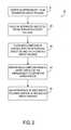
- FIG. 1is a side cross-sectional view of an apparatus according to some embodiments.
- FIG. 2is a diagram of a process according to some embodiments.
- FIG. 3is a top view of an IC package substrate according to some embodiments.
- FIG. 4is a close-up view of an IC package substrate according to some embodiments.
- FIG. 5is a top view of an IC package substrate having a plurality of interconnects attached thereto according to some embodiments.
- FIG. 6is a top view of an IC package substrate having a plurality of IC die attached thereto according to some embodiments.
- FIG. 7is a side cross-sectional view of an IC package substrate, a plurality of IC die, and a plurality of interconnects according to some embodiments.
- FIG. 8is a top view of an IC package substrate and mold compound according to some embodiments.
- FIG. 9is a side cross-sectional view of an apparatus according to some embodiments.
- FIG. 10Ais a side cross-sectional view of an apparatus according to some embodiments.
- FIG. 10Bis a side cross-sectional view of an apparatus according to some embodiments.
- FIG. 11is a side cross-sectional view of an apparatus according to some embodiments.
- FIG. 12is a side cross-sectional view of an IC package substrate, a plurality of IC die, and a plurality of interconnects according to some embodiments.
- FIG. 13is a top view of an IC package substrate and mold compound according to some embodiments.
- FIG. 14is a side cross-sectional view of elements of the FIG. 1 apparatus.
- FIG. 15is a diagram of a system according to some embodiments.
- FIG. 1is a cross-sectional side view of apparatus 1 according to some embodiments.
- Apparatus 1includes IC package 10 supporting IC die 11 and IC die 12 .
- IC die 11 and IC die 12may include integrated active and/or passive electrical devices and may be fabricated using any suitable material and fabrication techniques.
- IC die 10 and IC die 11may comprise any integrated electrical devices having any function.
- IC die 11comprises a microprocessor having a silicon substrate and IC die 12 comprises a cache memory having a silicon substrate.
- IC die 11is coupled to IC package 10 by die attach material 13 , which may comprise a die attach paste, film, or other material.
- IC die 11is electrically coupled to IC package 10 by wirebonds 15 . More specifically, an upper surface of IC die 11 includes electrical contacts (not shown) that are electrically coupled to the electrical devices integrated within IC die 11 . Wirebonds 15 are attached to respective ones of the electrical contacts and to respective electrical contacts (not shown) disposed on an upper surface of IC package 10 .
- IC die 21is coupled to IC die 11 by die attach material 14 , and is electrically coupled to IC package 10 by wirebonds 16 .
- Wirebonds 16are attached to respective ones of electrical contacts of IC die 12 and to respective electrical contacts (not shown) disposed on an upper surface of IC package 10 .
- one or more of wirebonds 16electrically couples an electrical contact of IC die 12 to an electrical contact of IC die 11 .
- IC package 10may comprise any ceramic, organic, and/or other suitable material.
- IC package 10comprises solder balls 17 for carrying power and I/O signals between elements of apparatus 1 and external devices.
- solder balls 17may be mounted directly to a motherboard (not shown) or onto an interposer that is in turn mounted directly to a motherboard.
- Alternative interconnectssuch as through-hole pins may be used instead of solder balls 17 to mount apparatus 1 to a motherboard, a socket, or another substrate.
- Interconnects 18are coupled to IC package 10 .
- Interconnects 18may comprise any suitable conductive material.
- interconnects 18comprise solder material.
- interconnects 18are illustrated as being substantially spherical, interconnects 18 may possess any suitable shape.
- interconnects 18may be coupled to an electrical contact of IC package 10 .
- the electrical contacts of IC package 10may be electrically coupled to electrical traces and routing vias within IC package 10 .
- the traces and viasmay electrically couple the electrical contacts to one or more of another electrical contact, solder balls 17 , and interconnects 18 .
- Mold compound 19is in contact with IC die 11 , IC die 12 , die attach material 13 , die attach material 14 , wirebonds 15 and 16 , and interconnects 18 .
- mold compound 19surrounds a perimeter of IC die 11 and IC die 12 .
- Mold compound 19may comprise a stiff material that provides stiffness to apparatus 1 and physical protection to the elements thereof.
- Apparatus 1also includes IC package 20 supporting IC die 21 and IC die 22 , which may include integrated active and/or passive electrical devices and may be fabricated using any suitable material and fabrication techniques.
- IC die 21is coupled to IC package 20 by die attach material 23
- IC die 22is coupled to IC die 21 by die attach material 24 .
- IC die 21 and IC die 22are electrically coupled to electrical contacts of IC package 20 by wirebonds 25 and wirebonds 26 , respectively.
- wirebonds 26may electrically couple IC die 22 to IC die 21 .
- IC package 20is coupled to mold compound 19 .
- Interconnects 27may also be coupled to electrical contacts of IC package 20 .
- Interconnects 27may comprise any suitable conductive material of any suitable shape, including but not limited to spherical solder material.
- Solder balls 28are also interconnects and may be electrically coupled to one or more electrical contacts of IC package 20 and to interconnects 18 for electrically coupling IC package 20 to interconnects 18 .
- Mold compound 19defines openings through which solder balls 28 may contact interconnects 18 .
- a first portion of at least one of interconnects 18is in contact with mold compound 19
- a second portionis not in contact with mold compound 19
- a third portionis in contact with IC package 10 .
- the above-mentioned second portionis in contact with one of solder balls 28 .
- the electrical contacts of IC package 20may be electrically coupled to electrical traces and routing vias within IC package 20 .
- the traces and viasmay electrically couple the electrical contacts to another electrical contact of IC package 20 , to an interconnect 27 , and/or to a solder ball 28 .
- traces and viaselectrically couple one or more of interconnects 27 at least to one of solder balls 28 .
- Mold compound 29is in contact with IC die 21 , IC die 22 , die attach material 23 , die attach material 24 , wirebonds 25 and 26 , and interconnects 27 . Mold compound 29 may surround a perimeter of IC die 21 and IC die 22 . A first portion of at least one of interconnects 27 is in contact with mold compound 29 , a second portion is not in contact with mold compound 29 , and a third portion is in contact with IC package 20 . The second portion is in contact with one of solder balls 31 coupled to IC package 30 .
- IC package 30supports IC die 32 and IC die 33 , which may include integrated active and/or passive electrical devices and may be fabricated using any suitable material and fabrication techniques.
- IC die 32is coupled to IC package 30 by die attach material 34
- IC die 33is coupled to IC die 32 by die attach material 35
- IC die 32 and IC die 33are electrically coupled to electrical contacts of IC package 30 by wirebonds 36 and wirebonds 37 , respectively.
- Mold compound 38is in contact with IC die 32 , IC die 33 , die attach material 34 , die attach material 35 , and wirebonds 36 and 37 . Mold compound 38 may surround a perimeter of IC die 32 and IC die 33 , and may provide stiffness to apparatus 1 and physical protection to the elements thereof.
- one or more of the IC die of apparatus 1are “flip-chip” IC die.
- a flip-chip IC diemay be electrically coupled to an adjacent IC die or IC package by an array of solder bumps affixed to the flip-chip IC die.
- Underfill materialmay be used to encapsulate the electrical coupling and to assist the mechanical coupling between the flip-chip IC die 10 and the adjacent IC die or IC package.
- FIG. 2is a diagram of process 40 to fabricate an apparatus according to some embodiments.
- Process 40may be executed by one or more devices, and all or a part of process 40 may be executed manually.
- Process 40may be executed by an entity different from an entity that manufactures the IC die used therein.
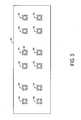
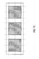
- FIG. 3shows IC package substrate 50 and integral IC packages 55 according to some embodiments of 41 .
- IC package substrate 50may be composed of any suitable IC package material, including but not limited to an organic laminated glass-weave polymer.
- IC packages 55are disposed in a matrix array package (MAP) configuration.
- IC packages 55include electrical contacts 60 disposed on upper surfaces thereof. Electrical contacts 60 of an IC package 55 may comprise any type of electrical contacts for electrically coupling elements to routing vias and electrical traces within the IC package substrate 55 .
- IC package substrate 50 and electrical contacts 60may be fabricated using any currently- or hereafter-known MAP fabrication method.
- FIG. 4is a close-up view of electrical contacts 60 of one IC package 55 according to some embodiments.
- Each of electrical contacts 60comprises wirebond pad 61 , fan-out trace 62 , and interconnect bonding pad 63 .
- Fan-out trace 62may be disposed under an upper surface of IC package 55 according to some embodiments.
- Some embodiments of IC package 55may include more or fewer electrical contacts 60 than shown.
- electrical contacts 60lack one or more of wirebond pad 61 , fan-out trace 62 , and interconnect bonding pad 63 .
- an electrical contact 60may include only wirebond pad 61 , only wirebond pad 61 and interconnect pad 63 , which may or may not be electrically coupled, only interconnect pad 63 , or elements in another configuration.
- electrical contacts 60may comprise an array suitable for coupling to a flip-chip IC die.
- An electrical contact 60 of an IC package 55may be electrically coupled to one or more of another electrical contact 60 of the IC package 55 , a via within the IC package 55 , a solder ball coupled to a lower surface of the IC package 55 , and other electrical elements.
- an interconnectmay be placed on one or more of electrical contacts 60 of an IC package 55 .
- the interconnectmay be similar to interconnects 18 and 27 described with respect to FIG. 1 .
- the interconnectmay be fabricated on the one or more of electrical contacts 60 according to some embodiments.
- An interconnectneed not be placed on each electrical contact 60 according to some embodiments.
- some embodimentsinclude interconnects placed in a non-symmetrical arrangement on an IC package 55 .
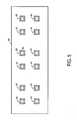
- FIG. 5is a top view of substrate 50 after 41 . Accordingly, interconnects 65 are shown coupled to IC packages 55 . As mentioned above, one or more of interconnects 65 are coupled to a respective one or more of electrical contacts 60 . In some embodiments, one or more IC packages 55 of substrate 50 include a different configuration of electrical contacts 60 than at least one other IC package 55 . In addition, an arrangement of interconnects 65 on at least one of IC packages 55 may differ from an arrangement of interconnects 65 on at least one other of IC packages 55 . An arrangement of interconnects 65 on two IC packages 55 may differ even in a case that the two IC packages 55 include an identical configuration of electrical contacts 60 .
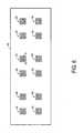
- An IC dieis placed on an IC package 55 at 42 .
- One or more IC diemay be placed on an IC package at 42 .
- FIG. 6shows IC die 70 and IC die 75 placed on each IC package 55 of IC package substrate 50 .
- the IC diemay be placed on respective ones of IC packages 55 using a pick-and-place machine.
- die attach materialmay be placed on an IC package 55 or on an IC die prior to placing an IC die thereon.
- FIG. 6also shows wirebonds between an IC die 70 and a respective IC package 55 and between an IC die 70 and a respective IC die 75 .
- FIG. 7is a cross-sectional side view further illustrating the arrangement of IC packages 55 , interconnects 65 , IC die 70 , and IC die 75 after 42 and according to some embodiments.
- underfill materialmay be thereafter dispensed on a corresponding IC package substrate 50 adjacent to the one or more IC die.
- the dispensed underfill materialmay comprise a capillary flow underfill material according to some embodiments, and energy may be applied thereto to transform the material into a protective inert polymer.
- FIG. 8illustrates an embodiment in which a mold is used to place a portion of mold compound 80 in contact with each “cluster” of IC packages 55 of IC package substrate 50 .
- FIG. 9is a cross-sectional side view of the FIG. 8 apparatus. As shown, mold compound 80 is in contact with IC package 55 , interconnects 65 , IC die 70 , and IC die 75 .
- Mold compound 80may be fully or partially cured at 43 in order to provide a suitable amount of physical stability to mold compound 80 . Curing may involve subjecting mold compound 80 to elevated temperatures. In some embodiments, interconnects 65 are also reflowed at 43 to improve a physical and an electrical connection between interconnects 65 and corresponding ones of electrical contacts 60 . Interconnects 65 and/or electrical connections between IC die 70 , IC die 75 , and IC package 55 may be partially and/or completely reflowed prior to 43 . Curing/reflow temperatures and sequences may depend on the specific fabrication techniques and materials used in various embodiments.
- FIGS. 10A and 10Billustrate two different embodiments of 44 .
- portions of mold compound 80are removed by laser drilling and/or etching techniques. The removal creates openings 85 in mold compound 80 , which extend to interconnects 65 .
- FIG. 10Bshows mold compound 80 and interconnects 65 after grinding at 44 .
- the embodiments of FIG 10 A and FIG. 10Bresult in an exposed upper portion of interconnects 65 .
- a first portion of at least one of interconnects 65is in contact with mold compound 80
- a second portionis not in contact with mold compound 80
- a third portionis in contact with IC package 55 .
- FIG. 11illustrates an embodiment in which process 40 proceeds directly from 43 to 45 .
- mold compound 80 placed on IC package 55presents a varying vertical profile.
- the vertical profileis lower than a vertical height of interconnects 65 at certain positions, which results in the exposure of an upper surface of interconnects 65 after 43 .
- FIG. 12is a side cross-sectional view of IC systems 90 through 93 and associated IC packages 100 through 103 according to some embodiments. Interconnects such as solder balls 110 have been attached to corresponding electrical contacts (not shown) of IC packages 100 through 103 using currently- or hereafter-known techniques, and in accordance with the apparatus in which IC systems 91 through 93 will be assembled. As noted above, the IC die, electrical contacts, vias, and inter-package conductive traces of each IC system may differ from those of another IC system.
- FIG. 12is a top view of an IC package substrate including IC systems 90 through 93 and further showing the cutting pattern according to some embodiments. Singulation may proceed using any currently- or hereafter-known methods, including saw singulation.
- FIG. 14illustrates cross-sectional side views of IC systems 90 , 91 and 92 according to some embodiments.
- IC systems 90 , 91 and 92may be assembled by creating metallurgical bonds between interconnects as indicated by the dotted lines of FIG. 14 .
- Substrates 100 and 102may also be joined to adjacent mold compound using adhesive.
- a resulting apparatusis according to some embodiments is illustrated in FIG. 1 .
- FIG. 15is a cross-sectional side view of system 200 according to some embodiments.
- System 200may comprise components of a mobile computing platform.
- System 200includes apparatus 1 as described above, memory 210 and motherboard 220 .
- Apparatus 1may comprise a “system on a chip”, wherein one or more IC die of apparatus 1 comprises a CPU, another one or more IC die comprises a memory, and another one or more IC die comprise an I/O controller.
- one or more IC die of apparatus 1may be fabricated using a different fabrication process than that used to fabricate at least one other IC die of apparatus 1 .
- Motherboard 220may electrically couple memory 210 to an IC die of apparatus 1 . More particularly, motherboard 220 may comprise a memory bus (not shown) that is electrically coupled to solder balls 17 and to memory 210 .
- Memory 210may comprise any type of memory for storing data, such as a Single Data Rate Random Access Memory, a Double Data Rate Random Access Memory, or a Programmable Read Only Memory.
Landscapes
- Engineering & Computer Science (AREA)
- Power Engineering (AREA)
- Microelectronics & Electronic Packaging (AREA)
- Computer Hardware Design (AREA)
- Physics & Mathematics (AREA)
- Condensed Matter Physics & Semiconductors (AREA)
- General Physics & Mathematics (AREA)
- Structures Or Materials For Encapsulating Or Coating Semiconductor Devices Or Solid State Devices (AREA)
Abstract
Description
- An integrated circuit (IC) packaging system electrically couples an IC die to various external elements, and may also provide thermal and physical protection to the IC die. In order to increase processing power and/or functionality within a given footprint, an IC packaging system may support two or more IC die. For example, a “stacked die” IC packaging system may include an IC package with two or more IC die stacked thereon. According to another example, a “stacked package” IC packaging system may include several IC packages stacked on one another, with each IC package having one or more IC die stacked thereon, and with adjacent IC packages being separated by a solid polymer interposer including conductive plugs for electrically coupling the adjacent IC packages.
- The foregoing IC packaging systems may present characteristics that may be undesirable in certain scenarios. These characteristics may include: limits on the relative sizes of adjacent IC die; wire bonding congestion on one or more IC packages; long wirebonds; inefficient fabrication processes; and/or limited ability to test IC die prior to final packaging.
FIG. 1 is a side cross-sectional view of an apparatus according to some embodiments.FIG. 2 is a diagram of a process according to some embodiments.FIG. 3 is a top view of an IC package substrate according to some embodiments.FIG. 4 is a close-up view of an IC package substrate according to some embodiments.FIG. 5 is a top view of an IC package substrate having a plurality of interconnects attached thereto according to some embodiments.FIG. 6 is a top view of an IC package substrate having a plurality of IC die attached thereto according to some embodiments.FIG. 7 is a side cross-sectional view of an IC package substrate, a plurality of IC die, and a plurality of interconnects according to some embodiments.FIG. 8 is a top view of an IC package substrate and mold compound according to some embodiments.FIG. 9 is a side cross-sectional view of an apparatus according to some embodiments.FIG. 10A is a side cross-sectional view of an apparatus according to some embodiments.FIG. 10B is a side cross-sectional view of an apparatus according to some embodiments.FIG. 11 is a side cross-sectional view of an apparatus according to some embodiments.FIG. 12 is a side cross-sectional view of an IC package substrate, a plurality of IC die, and a plurality of interconnects according to some embodiments.FIG. 13 is a top view of an IC package substrate and mold compound according to some embodiments.FIG. 14 is a side cross-sectional view of elements of theFIG. 1 apparatus.FIG. 15 is a diagram of a system according to some embodiments.FIG. 1 is a cross-sectional side view ofapparatus 1 according to some embodiments.Apparatus 1 includesIC package 10 supporting IC die11 and IC die12. IC die11 and IC die12 may include integrated active and/or passive electrical devices and may be fabricated using any suitable material and fabrication techniques. IC die10 and IC die11 may comprise any integrated electrical devices having any function. In some embodiments, IC die11 comprises a microprocessor having a silicon substrate and IC die12 comprises a cache memory having a silicon substrate.- IC die11 is coupled to
IC package 10 by dieattach material 13, which may comprise a die attach paste, film, or other material. IC die11 is electrically coupled toIC package 10 bywirebonds 15. More specifically, an upper surface of IC die11 includes electrical contacts (not shown) that are electrically coupled to the electrical devices integrated withinIC die 11. Wirebonds15 are attached to respective ones of the electrical contacts and to respective electrical contacts (not shown) disposed on an upper surface ofIC package 10. - Similarly, IC die21 is coupled to IC die11 by die
attach material 14, and is electrically coupled toIC package 10 bywirebonds 16. Wirebonds16 are attached to respective ones of electrical contacts of IC die12 and to respective electrical contacts (not shown) disposed on an upper surface ofIC package 10. In some embodiments, one or more ofwirebonds 16 electrically couples an electrical contact of IC die12 to an electrical contact of IC die11. IC package 10 may comprise any ceramic, organic, and/or other suitable material.IC package 10 comprisessolder balls 17 for carrying power and I/O signals between elements ofapparatus 1 and external devices. For example,solder balls 17 may be mounted directly to a motherboard (not shown) or onto an interposer that is in turn mounted directly to a motherboard. Alternative interconnects such as through-hole pins may be used instead ofsolder balls 17 to mountapparatus 1 to a motherboard, a socket, or another substrate.Interconnects 18 are coupled toIC package 10.Interconnects 18 may comprise any suitable conductive material. According to some embodiments,interconnects 18 comprise solder material. Althoughinterconnects 18 are illustrated as being substantially spherical,interconnects 18 may possess any suitable shape.- One or more of
interconnects 18 may be coupled to an electrical contact ofIC package 10. In this regard, the electrical contacts ofIC package 10 may be electrically coupled to electrical traces and routing vias withinIC package 10. The traces and vias may electrically couple the electrical contacts to one or more of another electrical contact,solder balls 17, and interconnects18. - Mold
compound 19 is in contact with IC die11, IC die12, dieattach material 13, dieattach material 14,wirebonds interconnects 18. In some embodiments,mold compound 19 surrounds a perimeter of IC die11 and IC die12.Mold compound 19 may comprise a stiff material that provides stiffness toapparatus 1 and physical protection to the elements thereof. Apparatus 1 also includesIC package 20 supporting IC die21 and IC die22, which may include integrated active and/or passive electrical devices and may be fabricated using any suitable material and fabrication techniques. IC die21 is coupled toIC package 20 by dieattach material 23, and IC die22 is coupled to IC die21 by dieattach material 24. IC die21 and IC die22 are electrically coupled to electrical contacts ofIC package 20 bywirebonds 25 andwirebonds 26, respectively. One or more ofwirebonds 26 may electrically couple IC die22 to IC die21. In some embodiments,IC package 20 is coupled tomold compound 19.Interconnects 27 may also be coupled to electrical contacts ofIC package 20.Interconnects 27 may comprise any suitable conductive material of any suitable shape, including but not limited to spherical solder material.Solder balls 28 are also interconnects and may be electrically coupled to one or more electrical contacts ofIC package 20 and to interconnects18 for electrically couplingIC package 20 to interconnects18. Moldcompound 19 defines openings through whichsolder balls 28 may contactinterconnects 18. As a result of the foregoing arrangement, a first portion of at least one ofinterconnects 18 is in contact withmold compound 19, a second portion is not in contact withmold compound 19, and a third portion is in contact withIC package 10. According to the embodiment ofFIG. 1 , the above-mentioned second portion is in contact with one ofsolder balls 28.- The electrical contacts of
IC package 20 may be electrically coupled to electrical traces and routing vias withinIC package 20. The traces and vias may electrically couple the electrical contacts to another electrical contact ofIC package 20, to aninterconnect 27, and/or to asolder ball 28. For example, according to some embodiments, traces and vias electrically couple one or more ofinterconnects 27 at least to one ofsolder balls 28. Mold compound 29 is in contact with IC die21, IC die22, die attachmaterial 23, die attachmaterial 24, wirebonds25 and26, and interconnects27.Mold compound 29 may surround a perimeter of IC die21 and IC die22. A first portion of at least one ofinterconnects 27 is in contact withmold compound 29, a second portion is not in contact withmold compound 29, and a third portion is in contact withIC package 20. The second portion is in contact with one ofsolder balls 31 coupled toIC package 30.IC package 30 supports IC die32 and IC die33, which may include integrated active and/or passive electrical devices and may be fabricated using any suitable material and fabrication techniques. IC die32 is coupled toIC package 30 by die attachmaterial 34, and IC die33 is coupled to IC die32 by die attachmaterial 35. IC die32 and IC die33 are electrically coupled to electrical contacts ofIC package 30 bywirebonds 36 andwirebonds 37, respectively.Mold compound 38 is in contact with IC die32, IC die33, die attachmaterial 34, die attachmaterial 35, and wirebonds36 and37.Mold compound 38 may surround a perimeter of IC die32 and IC die33, and may provide stiffness toapparatus 1 and physical protection to the elements thereof.- According to some embodiments, one or more of the IC die of
apparatus 1 are “flip-chip” IC die. A flip-chip IC die may be electrically coupled to an adjacent IC die or IC package by an array of solder bumps affixed to the flip-chip IC die. Underfill material may be used to encapsulate the electrical coupling and to assist the mechanical coupling between the flip-chip IC die10 and the adjacent IC die or IC package. FIG. 2 is a diagram ofprocess 40 to fabricate an apparatus according to some embodiments.Process 40 may be executed by one or more devices, and all or a part ofprocess 40 may be executed manually.Process 40 may be executed by an entity different from an entity that manufactures the IC die used therein.- Initially, at41, an interconnect is coupled to an IC package.
FIG. 3 showsIC package substrate 50 and integral IC packages55 according to some embodiments of41.IC package substrate 50 may be composed of any suitable IC package material, including but not limited to an organic laminated glass-weave polymer. - IC packages55 are disposed in a matrix array package (MAP) configuration. IC packages55 include
electrical contacts 60 disposed on upper surfaces thereof.Electrical contacts 60 of anIC package 55 may comprise any type of electrical contacts for electrically coupling elements to routing vias and electrical traces within theIC package substrate 55. According to some embodiments,IC package substrate 50 andelectrical contacts 60 may be fabricated using any currently- or hereafter-known MAP fabrication method. FIG. 4 is a close-up view ofelectrical contacts 60 of oneIC package 55 according to some embodiments. Each ofelectrical contacts 60 compriseswirebond pad 61, fan-out trace 62, andinterconnect bonding pad 63. Fan-out trace 62 may be disposed under an upper surface ofIC package 55 according to some embodiments. Some embodiments ofIC package 55 may include more or fewerelectrical contacts 60 than shown.- Moreover, some embodiments of
electrical contacts 60 lack one or more ofwirebond pad 61, fan-out trace 62, andinterconnect bonding pad 63. For example, anelectrical contact 60 may includeonly wirebond pad 61, only wirebondpad 61 andinterconnect pad 63, which may or may not be electrically coupled, onlyinterconnect pad 63, or elements in another configuration. In some embodiments,electrical contacts 60 may comprise an array suitable for coupling to a flip-chip IC die. Anelectrical contact 60 of anIC package 55 may be electrically coupled to one or more of anotherelectrical contact 60 of theIC package 55, a via within theIC package 55, a solder ball coupled to a lower surface of theIC package 55, and other electrical elements. - At41, an interconnect may be placed on one or more of
electrical contacts 60 of anIC package 55. The interconnect may be similar tointerconnects FIG. 1 . The interconnect may be fabricated on the one or more ofelectrical contacts 60 according to some embodiments. An interconnect need not be placed on eachelectrical contact 60 according to some embodiments. Moreover, some embodiments include interconnects placed in a non-symmetrical arrangement on anIC package 55. FIG. 5 is a top view ofsubstrate 50 after41. Accordingly, interconnects65 are shown coupled to IC packages55. As mentioned above, one or more ofinterconnects 65 are coupled to a respective one or more ofelectrical contacts 60. In some embodiments, one or more IC packages55 ofsubstrate 50 include a different configuration ofelectrical contacts 60 than at least oneother IC package 55. In addition, an arrangement ofinterconnects 65 on at least one ofIC packages 55 may differ from an arrangement ofinterconnects 65 on at least one other of IC packages55. An arrangement ofinterconnects 65 on twoIC packages 55 may differ even in a case that the twoIC packages 55 include an identical configuration ofelectrical contacts 60.- An IC die is placed on an
IC package 55 at42. One or more IC die may be placed on an IC package at42.FIG. 6 shows IC die70 and IC die75 placed on eachIC package 55 ofIC package substrate 50. The IC die may be placed on respective ones of IC packages55 using a pick-and-place machine. As described with respect toFIG. 1 , die attach material may be placed on anIC package 55 or on an IC die prior to placing an IC die thereon.FIG. 6 also shows wirebonds between anIC die 70 and arespective IC package 55 and between anIC die 70 and a respective IC die75. The number of die, type of die, and/or wirebond arrangement associated with anIC package 55 may differ from at least oneother IC package 55.FIG. 7 is a cross-sectional side view further illustrating the arrangement of IC packages55, interconnects65, IC die70, and IC die75 after42 and according to some embodiments. - In a case that one or more of the IC die placed at42 is a flip-chip die, underfill material may be thereafter dispensed on a corresponding
IC package substrate 50 adjacent to the one or more IC die. The dispensed underfill material may comprise a capillary flow underfill material according to some embodiments, and energy may be applied thereto to transform the material into a protective inert polymer. - At43, mold compound is placed in contact with an IC package and with IC die coupled to the IC package.
FIG. 8 illustrates an embodiment in which a mold is used to place a portion ofmold compound 80 in contact with each “cluster” of IC packages55 ofIC package substrate 50.FIG. 9 is a cross-sectional side view of theFIG. 8 apparatus. As shown,mold compound 80 is in contact withIC package 55, interconnects65, IC die70, and IC die75. Mold compound 80 may be fully or partially cured at43 in order to provide a suitable amount of physical stability tomold compound 80. Curing may involve subjectingmold compound 80 to elevated temperatures. In some embodiments, interconnects65 are also reflowed at43 to improve a physical and an electrical connection betweeninterconnects 65 and corresponding ones ofelectrical contacts 60.Interconnects 65 and/or electrical connections between IC die70, IC die75, andIC package 55 may be partially and/or completely reflowed prior to43. Curing/reflow temperatures and sequences may depend on the specific fabrication techniques and materials used in various embodiments.- Next, at44,
mold compound 80 is removed from an upper portion of an interconnect to expose the upper portion.FIGS. 10A and 10B illustrate two different embodiments of44. InFIG. 10A , portions ofmold compound 80 are removed by laser drilling and/or etching techniques. The removal createsopenings 85 inmold compound 80, which extend to interconnects65.FIG. 10B showsmold compound 80 and interconnects65 after grinding at44. The embodiments of FIG10A andFIG. 10B result in an exposed upper portion ofinterconnects 65. Moreover, a first portion of at least one ofinterconnects 65 is in contact withmold compound 80, a second portion is not in contact withmold compound 80, and a third portion is in contact withIC package 55. FIG. 11 illustrates an embodiment in whichprocess 40 proceeds directly from43 to45. In this regard,mold compound 80 placed onIC package 55 presents a varying vertical profile. The vertical profile is lower than a vertical height ofinterconnects 65 at certain positions, which results in the exposure of an upper surface ofinterconnects 65 after43.- Appropriate interconnects are then added to a lower surface of an
IC package 55 at45. The interconnects may be added depending on a design of an apparatus in whichIC package 55 is to be assembled.FIG. 12 is a side cross-sectional view ofIC systems 90 through93 and associated IC packages100 through103 according to some embodiments. Interconnects such assolder balls 110 have been attached to corresponding electrical contacts (not shown) ofIC packages 100 through103 using currently- or hereafter-known techniques, and in accordance with the apparatus in whichIC systems 91 through93 will be assembled. As noted above, the IC die, electrical contacts, vias, and inter-package conductive traces of each IC system may differ from those of another IC system. - One or more of
IC systems 90 through93 may be singulated afterprocess 40. The dashed lines ofFIG. 12 represent a cutting pattern forsingulating IC systems 90 through93.FIG. 13 is a top view of an IC package substrate includingIC systems 90 through93 and further showing the cutting pattern according to some embodiments. Singulation may proceed using any currently- or hereafter-known methods, including saw singulation. FIG. 14 illustrates cross-sectional side views ofIC systems IC systems FIG. 14 .Substrates FIG. 1 .FIG. 15 is a cross-sectional side view ofsystem 200 according to some embodiments.System 200 may comprise components of a mobile computing platform.System 200 includesapparatus 1 as described above,memory 210 andmotherboard 220.Apparatus 1 may comprise a “system on a chip”, wherein one or more IC die ofapparatus 1 comprises a CPU, another one or more IC die comprises a memory, and another one or more IC die comprise an I/O controller. According to some embodiments, one or more IC die ofapparatus 1 may be fabricated using a different fabrication process than that used to fabricate at least one other IC die ofapparatus 1.Motherboard 220 may electrically couplememory 210 to an IC die ofapparatus 1. More particularly,motherboard 220 may comprise a memory bus (not shown) that is electrically coupled tosolder balls 17 and tomemory 210.Memory 210 may comprise any type of memory for storing data, such as a Single Data Rate Random Access Memory, a Double Data Rate Random Access Memory, or a Programmable Read Only Memory.- The several embodiments described herein are solely for the purpose of illustration. The various features described herein need not all be used together, and any one or more of those features may be incorporated in a single embodiment. Some embodiments may include any currently or hereafter-known versions of the elements described herein. Therefore, persons skilled in the art will recognize from this description that other embodiments may be practiced with various modifications and alterations.
Claims (19)
1. An apparatus comprising:
an integrated circuit die;
an integrated circuit package coupled to the integrated circuit die;
mold compound in contact with the integrated circuit die and the integrated circuit package; and
an interconnect coupled to the integrated circuit package,
wherein a first portion of the interconnect is in contact with the mold compound, wherein a second portion of the interconnect is not in contact with the mold compound, and wherein a third portion of the interconnect is in contact with the integrated circuit package.
2. An apparatus according toclaim 1 , wherein the second portion is an upper portion of the interconnect and the third portion is a lower portion of the interconnect.
3. An apparatus according toclaim 1 , further comprising:
a second integrated circuit package;
a second interconnect coupled to the second integrated circuit package,
wherein the second interconnect is coupled to the first interconnect.
4. An apparatus according toclaim 3 , wherein the second integrated circuit package is coupled to the mold compound.
5. An apparatus according toclaim 3 , further comprising:
a second integrated circuit die coupled to the second integrated circuit package;
second mold compound in contact with the second integrated circuit die and the second integrated circuit package; and
a third interconnect coupled to the second integrated circuit package,
wherein a first portion of the third interconnect is in contact with the second mold compound, and wherein a second portion of the third interconnect is not in contact with the second mold compound, and wherein a third portion of the third interconnect is in contact with the second integrated circuit package.
6. An apparatus according toclaim 5 , further comprising:
a third integrated circuit package;
a fourth interconnect coupled to the third integrated circuit package,
wherein the fourth interconnect is coupled to the third interconnect.
7. An apparatus according toclaim 1 , further comprising:
a second integrated circuit die coupled to the integrated circuit die, in contact with the mold compound, and electrically coupled to the integrated circuit package.
8. An apparatus comprising:
an integrated circuit package substrate;
a plurality of integrated circuit die coupled to the integrated circuit package substrate;
mold compound in contact with the plurality of integrated circuit die and the integrated circuit package substrate; and
an interconnect coupled to the integrated circuit package substrate and electrically coupled to one of the plurality of integrated circuit die,
wherein a first portion of the interconnect is in contact with the mold compound, wherein a second portion of the interconnect is not in contact with the mold compound, and wherein a third portion of the interconnect is in contact with the integrated circuit package.
9. An apparatus according toclaim 8 , further comprising:
underfill material disposed between the first face of each of the plurality of integrated circuit die and the integrated circuit package substrate.
10. An apparatus according toclaim 8 , further comprising:
a second integrated circuit die coupled to the integrated circuit die, in contact with the mold compound, and electrically coupled to the integrated circuit package.
11. A method comprising:
coupling an interconnect to an integrated circuit package;
placing an integrated circuit die on the integrated package; and
placing mold compound on the integrated circuit package and in contact with the integrated circuit die,
wherein a first portion of the interconnect is in contact with the mold compound, wherein a second portion of the interconnect is not in contact with the mold compound, and wherein a third portion of the interconnect is in contact with the integrated circuit package.
12. A method according toclaim 11 , wherein placing the mold compound on the integrated circuit package comprises placing the mold compound over the interconnect, and further comprising:
removing mold compound from an upper portion of the interconnect to expose the upper portion.
13. A method according toclaim 11 , further comprising:
coupling a second interconnect to the first interconnect, the second interconnect coupled to a second integrated circuit package.
14. A method according toclaim 13 , further comprising the second integrated circuit to the mold compound.
15. A system comprising:
an integrated circuit die;
an integrated circuit package coupled to the integrated circuit die;
mold compound in contact with the integrated circuit die and the integrated circuit package; and
an interconnect coupled to the integrated circuit package; and
a double data rate memory electrically coupled to the integrated circuit die,
wherein a first portion of the interconnect is in contact with the mold compound, wherein a second portion of the interconnect is not in contact with the mold compound, and wherein a third portion of the interconnect is in contact with the integrated circuit package.
16. A system according toclaim 15 , further comprising:
a second integrated circuit die;
a second integrated circuit package coupled to the second integrated circuit die;
a second interconnect coupled to the second integrated circuit package,
wherein the second interconnect is coupled to the first interconnect.
17. A system according toclaim 16 , wherein the second integrated circuit package is coupled to the mold compound.
18. A system according toclaim 15 , further comprising:
a second integrated circuit die coupled to the integrated circuit die, in contact with the mold compound, and electrically coupled to the integrated circuit package.
19. A system according toclaim 15 , further comprising:
a motherboard electrically coupled to the integrated circuit die and to the memory.
Priority Applications (1)
| Application Number | Priority Date | Filing Date | Title |
|---|---|---|---|
| US10/728,324US7345361B2 (en) | 2003-12-04 | 2003-12-04 | Stackable integrated circuit packaging |
Applications Claiming Priority (1)
| Application Number | Priority Date | Filing Date | Title |
|---|---|---|---|
| US10/728,324US7345361B2 (en) | 2003-12-04 | 2003-12-04 | Stackable integrated circuit packaging |
Publications (2)
| Publication Number | Publication Date |
|---|---|
| US20050121764A1true US20050121764A1 (en) | 2005-06-09 |
| US7345361B2 US7345361B2 (en) | 2008-03-18 |
Family
ID=34633681
Family Applications (1)
| Application Number | Title | Priority Date | Filing Date |
|---|---|---|---|
| US10/728,324Expired - LifetimeUS7345361B2 (en) | 2003-12-04 | 2003-12-04 | Stackable integrated circuit packaging |
Country Status (1)
| Country | Link |
|---|---|
| US (1) | US7345361B2 (en) |
Cited By (104)
| Publication number | Priority date | Publication date | Assignee | Title |
|---|---|---|---|---|
| US20050112880A1 (en)* | 2003-10-13 | 2005-05-26 | Wood Dustin P. | Selective plating of package terminals |
| US20060033193A1 (en)* | 2004-08-11 | 2006-02-16 | Daewoong Suh | Methods and apparatuses for providing stacked-die devices |
| US20060208358A1 (en)* | 2005-03-21 | 2006-09-21 | Nokia Corporation | Stacked package integrated circuit |
| DE102005050637A1 (en)* | 2005-10-20 | 2006-11-09 | Infineon Technologies Ag | Semiconductor device with wiring substrate and solder balls and method for producing the semiconductor device |
| US20060278991A1 (en)* | 2005-06-13 | 2006-12-14 | Yong-Chai Kwon | Stack circuit member and method |
| US20070052081A1 (en)* | 2005-09-01 | 2007-03-08 | Gerber Mark A | Package-on-package semiconductor assembly |
| DE102005051414B3 (en)* | 2005-10-25 | 2007-04-12 | Infineon Technologies Ag | Semiconductor component with wiring substrate and solder balls and production processes has central plastic mass and lower film template for lower solder ball arrangement |
| US20070216006A1 (en)* | 2006-03-17 | 2007-09-20 | Stats Chippac Ltd. | Integrated circuit package on package system |
| US20070289777A1 (en)* | 2006-06-14 | 2007-12-20 | Stats Chippac Ltd. | Package-on-package system |
| US20080036065A1 (en)* | 2006-08-10 | 2008-02-14 | Infineon Technologies Ag | Electronic device and method for producing a device |
| US20080076208A1 (en)* | 2006-09-27 | 2008-03-27 | Yen-Yi Wu | Method of making a semiconductor package and method of making a semiconductor device |
| US20080086870A1 (en)* | 2006-10-17 | 2008-04-17 | Broadcom Corporation | Single footprint family of integrated power modules |
| US20080230887A1 (en)* | 2007-03-23 | 2008-09-25 | Advanced Semiconductor Engineering, Inc. | Semiconductor package and the method of making the same |
| US20080315387A1 (en)* | 2006-05-01 | 2008-12-25 | Texas Instruments Incorporated | Semiconductor Package-on-Package System Including Integrated Passive Components |
| US20090146301A1 (en)* | 2007-12-11 | 2009-06-11 | Panasonic Corporation | Semiconductor device and method of manufacturing the same |
| US20090184412A1 (en)* | 2007-10-25 | 2009-07-23 | Rohm Co., Ltd. | Resin-seal type semiconductor device |
| US20090206455A1 (en)* | 2008-02-19 | 2009-08-20 | Texas Instruments Incorporated | Integrated circuit stacked package precursors and stacked packaged devices and systems therefrom |
| US20090283900A1 (en)* | 2008-05-15 | 2009-11-19 | Panasonic Corporation | Semiconductor device and manufacturing method for semiconductor device |
| CN100578745C (en)* | 2007-10-30 | 2010-01-06 | 日月光半导体制造股份有限公司 | Method for manufacturing semiconductor device and semiconductor device |
| US20100000775A1 (en)* | 2008-07-03 | 2010-01-07 | Advanced Semiconductor Engineering, Inc. | Circuit substrate and method of fabricating the same and chip package structure |
| US7652361B1 (en) | 2006-03-03 | 2010-01-26 | Amkor Technology, Inc. | Land patterns for a semiconductor stacking structure and method therefor |
| US20100038781A1 (en)* | 2008-08-14 | 2010-02-18 | Dongsam Park | Integrated circuit packaging system having a cavity |
| US20100171207A1 (en)* | 2009-01-07 | 2010-07-08 | Chi-Chih Shen | Stackable semiconductor device packages |
| US20100171206A1 (en)* | 2009-01-07 | 2010-07-08 | Chi-Chih Chu | Package-on-Package Device, Semiconductor Package, and Method for Manufacturing The Same |
| US20100171205A1 (en)* | 2009-01-07 | 2010-07-08 | Kuang-Hsiung Chen | Stackable Semiconductor Device Packages |
| US20110049704A1 (en)* | 2009-08-31 | 2011-03-03 | Advanced Semiconductor Engineering, Inc. | Semiconductor device packages with integrated heatsinks |
| US20110117700A1 (en)* | 2009-11-18 | 2011-05-19 | Advanced Semiconductor Engineering, Inc. | Stackable semiconductor device packages |
| US20110156230A1 (en)* | 2009-12-31 | 2011-06-30 | Stmicroelectronics Asia Pacific Pte, Ltd. | Multi-stacked semiconductor dice scale package structure and method of manufacturing same |
| US20110156250A1 (en)* | 2009-12-31 | 2011-06-30 | Stmicroelectronics Asia Pacific Pte. Ltd. | Flip-chip fan-out wafer level package for package-on-package applications, and method of manufacture |
| US20110156251A1 (en)* | 2009-12-31 | 2011-06-30 | Chi-Chih Chu | Semiconductor Package |
| US20110157452A1 (en)* | 2009-12-31 | 2011-06-30 | Stmicroelectronics Asia Pacific Pte. Ltd. | Fan-out wafer level package for an optical sensor and method of manufacture thereof |
| US20110156240A1 (en)* | 2009-12-31 | 2011-06-30 | Stmicroelectronics Asia Pacific Pte. Ltd. | Reliable large die fan-out wafer level package and method of manufacture |
| US20110157853A1 (en)* | 2009-12-31 | 2011-06-30 | Stmicroelectronics Asia Pacific Pte Ltd. | Fan-out wafer level package with polymeric layer for high reliability |
| US20110193205A1 (en)* | 2010-02-10 | 2011-08-11 | Advanced Semiconductor Engineering, Inc. | Semiconductor device packages having stacking functionality and including interposer |
| US20110260303A1 (en)* | 2010-04-23 | 2011-10-27 | Stats Chippac, Ltd. | Semiconductor Device and Method of Forming Openings in Thermally-Conductive Frame of FO-WLCSP to Dissipate Heat and Reduce Package Height |
| US20120025374A1 (en)* | 2010-06-02 | 2012-02-02 | Bae Johyun | Integrated circuit packaging system with rounded interconnect |
| US20120049348A1 (en)* | 2010-08-31 | 2012-03-01 | Samsung Electronics Co., Ltd. | Package having elastic members for vias, package on package comprising the same, and methods of fabricating the same |
| US20120061855A1 (en)* | 2010-09-14 | 2012-03-15 | Byung Tai Do | Integrated circuit packaging system with film encapsulation and method of manufacture thereof |
| US20120146206A1 (en)* | 2010-12-13 | 2012-06-14 | Tessera Research Llc | Pin attachment |
| US20120205795A1 (en)* | 2011-02-15 | 2012-08-16 | Samsung Electronics Co., Ltd. | Stacked package and method of manufacturing the same |
| US8278746B2 (en) | 2010-04-02 | 2012-10-02 | Advanced Semiconductor Engineering, Inc. | Semiconductor device packages including connecting elements |
| JP2013021237A (en)* | 2011-07-13 | 2013-01-31 | Apic Yamada Corp | Semiconductor device and method of manufacturing the same |
| US20130043587A1 (en)* | 2011-08-19 | 2013-02-21 | Huahung Kao | Package-on-package structures |
| EP2521170A4 (en)* | 2009-12-29 | 2013-06-19 | Hana Micron Inc | Pop package and manufacturing method thereof |
| US20130200509A1 (en)* | 2012-02-02 | 2013-08-08 | Samsung Electronics Co., Ltd. | Semiconductor package |
| US8557629B1 (en)* | 2010-12-03 | 2013-10-15 | Amkor Technology, Inc. | Semiconductor device having overlapped via apertures |
| US8569885B2 (en) | 2010-10-29 | 2013-10-29 | Advanced Semiconductor Engineering, Inc. | Stacked semiconductor packages and related methods |
| US20130292833A1 (en)* | 2012-05-04 | 2013-11-07 | Samsung Electronics Co., Ltd. | Semiconductor device and method of fabricating the same |
| US8623706B2 (en) | 2010-11-15 | 2014-01-07 | Tessera, Inc. | Microelectronic package with terminals on dielectric mass |
| US8624374B2 (en) | 2010-04-02 | 2014-01-07 | Advanced Semiconductor Engineering, Inc. | Semiconductor device packages with fan-out and with connecting elements for stacking and manufacturing methods thereof |
| US8643167B2 (en) | 2011-01-06 | 2014-02-04 | Advanced Semiconductor Engineering, Inc. | Semiconductor package with through silicon vias and method for making the same |
| US20140103527A1 (en)* | 2012-03-23 | 2014-04-17 | Stats Chippac, Ltd. | Semiconductor Device and Method of Forming a POP Device with Embedded Vertical Interconnect Units |
| US8772152B2 (en) | 2012-02-24 | 2014-07-08 | Invensas Corporation | Method for package-on-package assembly with wire bonds to encapsulation surface |
| US8836136B2 (en) | 2011-10-17 | 2014-09-16 | Invensas Corporation | Package-on-package assembly with wire bond vias |
| US20140264856A1 (en)* | 2013-03-14 | 2014-09-18 | Taiwan Semiconductor Manufacturing Company, Ltd. | Package-on-Package Structures and Methods for Forming the Same |
| US8878353B2 (en) | 2012-12-20 | 2014-11-04 | Invensas Corporation | Structure for microelectronic packaging with bond elements to encapsulation surface |
| US8883563B1 (en) | 2013-07-15 | 2014-11-11 | Invensas Corporation | Fabrication of microelectronic assemblies having stack terminals coupled by connectors extending through encapsulation |
| US8907466B2 (en) | 2010-07-19 | 2014-12-09 | Tessera, Inc. | Stackable molded microelectronic packages |
| US8927337B2 (en) | 2004-11-03 | 2015-01-06 | Tessera, Inc. | Stacked packaging improvements |
| US20150041972A1 (en)* | 2013-08-12 | 2015-02-12 | Siliconware Precision Industries Co., Ltd. | Semiconductor package and fabrication method thereof |
| US8975738B2 (en) | 2012-11-12 | 2015-03-10 | Invensas Corporation | Structure for microelectronic packaging with terminals on dielectric mass |
| US9023691B2 (en) | 2013-07-15 | 2015-05-05 | Invensas Corporation | Microelectronic assemblies with stack terminals coupled by connectors extending through encapsulation |
| US9034696B2 (en) | 2013-07-15 | 2015-05-19 | Invensas Corporation | Microelectronic assemblies having reinforcing collars on connectors extending through encapsulation |
| US20150147845A1 (en)* | 2013-11-26 | 2015-05-28 | Texas Instruments Incorporated | Dual sided embedded die and fabrication of same background |
| US20150187723A1 (en)* | 2012-12-28 | 2015-07-02 | Taiwan Semiconductor Manufacturing Company, Ltd. | Package on Package Bonding Structure and Method for Forming the Same |
| US9082753B2 (en) | 2013-11-12 | 2015-07-14 | Invensas Corporation | Severing bond wire by kinking and twisting |
| US9087815B2 (en) | 2013-11-12 | 2015-07-21 | Invensas Corporation | Off substrate kinking of bond wire |
| US9159708B2 (en) | 2010-07-19 | 2015-10-13 | Tessera, Inc. | Stackable molded microelectronic packages with area array unit connectors |
| US9171792B2 (en) | 2011-02-28 | 2015-10-27 | Advanced Semiconductor Engineering, Inc. | Semiconductor device packages having a side-by-side device arrangement and stacking functionality |
| US9196597B2 (en) | 2010-01-13 | 2015-11-24 | Advanced Semiconductor Engineering, Inc. | Semiconductor package with single sided substrate design and manufacturing methods thereof |
| US9214454B2 (en) | 2014-03-31 | 2015-12-15 | Invensas Corporation | Batch process fabrication of package-on-package microelectronic assemblies |
| US9218988B2 (en)* | 2005-12-23 | 2015-12-22 | Tessera, Inc. | Microelectronic packages and methods therefor |
| US9224717B2 (en) | 2011-05-03 | 2015-12-29 | Tessera, Inc. | Package-on-package assembly with wire bonds to encapsulation surface |
| US9349611B2 (en) | 2010-03-22 | 2016-05-24 | Advanced Semiconductor Engineering, Inc. | Stackable semiconductor package and manufacturing method thereof |
| US9349706B2 (en) | 2012-02-24 | 2016-05-24 | Invensas Corporation | Method for package-on-package assembly with wire bonds to encapsulation surface |
| US9362161B2 (en)* | 2014-03-20 | 2016-06-07 | Stats Chippac, Ltd. | Semiconductor device and method of forming 3D dual side die embedded build-up semiconductor package |
| US9391008B2 (en) | 2012-07-31 | 2016-07-12 | Invensas Corporation | Reconstituted wafer-level package DRAM |
| US9412714B2 (en) | 2014-05-30 | 2016-08-09 | Invensas Corporation | Wire bond support structure and microelectronic package including wire bonds therefrom |
| US20160276403A1 (en)* | 2012-08-15 | 2016-09-22 | Epistar Corporation | Method of forming a light-emitting device |
| US20160276258A1 (en)* | 2012-06-21 | 2016-09-22 | STATS ChipPAC Pte. Ltd. | Semiconductor Device and Method of Forming an Embedded SOP Fan-Out Package |
| US20160300823A1 (en)* | 2014-07-14 | 2016-10-13 | Apple Inc. | Package-on-package options with multiple layer 3-d stacking |
| US9502390B2 (en) | 2012-08-03 | 2016-11-22 | Invensas Corporation | BVA interposer |
| US9530749B2 (en) | 2015-04-28 | 2016-12-27 | Invensas Corporation | Coupling of side surface contacts to a circuit platform |
| US9583411B2 (en) | 2014-01-17 | 2017-02-28 | Invensas Corporation | Fine pitch BVA using reconstituted wafer with area array accessible for testing |
| US9601454B2 (en) | 2013-02-01 | 2017-03-21 | Invensas Corporation | Method of forming a component having wire bonds and a stiffening layer |
| US9646917B2 (en) | 2014-05-29 | 2017-05-09 | Invensas Corporation | Low CTE component with wire bond interconnects |
| US9659848B1 (en) | 2015-11-18 | 2017-05-23 | Invensas Corporation | Stiffened wires for offset BVA |
| US9685365B2 (en) | 2013-08-08 | 2017-06-20 | Invensas Corporation | Method of forming a wire bond having a free end |
| US9728527B2 (en) | 2013-11-22 | 2017-08-08 | Invensas Corporation | Multiple bond via arrays of different wire heights on a same substrate |
| US9837303B2 (en) | 2012-03-23 | 2017-12-05 | STATS ChipPAC Pte. Ltd. | Semiconductor method and device of forming a fan-out device with PWB vertical interconnect units |
| US9852969B2 (en) | 2013-11-22 | 2017-12-26 | Invensas Corporation | Die stacks with one or more bond via arrays of wire bond wires and with one or more arrays of bump interconnects |
| US9865525B2 (en) | 2012-03-23 | 2018-01-09 | STATS ChipPAC Pte. Ltd. | Semiconductor method and device of forming a fan-out PoP device with PWB vertical interconnect units |
| US20180053753A1 (en)* | 2016-08-16 | 2018-02-22 | Freescale Semiconductor, Inc. | Stackable molded packages and methods of manufacture thereof |
| US20180096950A1 (en)* | 2016-10-04 | 2018-04-05 | Skyworks Solutions, Inc. | Radio-frequency device with dual-sided overmold structure |
| US10008477B2 (en) | 2013-09-16 | 2018-06-26 | Invensas Corporation | Microelectronic element with bond elements to encapsulation surface |
| US10026717B2 (en) | 2013-11-22 | 2018-07-17 | Invensas Corporation | Multiple bond via arrays of different wire heights on a same substrate |
| US10049964B2 (en) | 2012-03-23 | 2018-08-14 | STATS ChipPAC Pte. Ltd. | Semiconductor device and method of forming a fan-out PoP device with PWB vertical interconnect units |
| US10332854B2 (en) | 2015-10-23 | 2019-06-25 | Invensas Corporation | Anchoring structure of fine pitch bva |
| US20190206827A1 (en)* | 2017-12-29 | 2019-07-04 | Intel Corporation | Semiconductor package with externally accessible wirebonds |
| CN110233142A (en)* | 2013-03-14 | 2019-09-13 | 台湾积体电路制造股份有限公司 | Laminated packaging structure and forming method thereof |
| US10460958B2 (en) | 2013-08-07 | 2019-10-29 | Invensas Corporation | Method of manufacturing embedded packaging with preformed vias |
| KR20200041265A (en)* | 2018-10-10 | 2020-04-21 | 타이완 세미콘덕터 매뉴팩쳐링 컴퍼니 리미티드 | Compute-in-memory packages and methods forming the same |
| US10631410B2 (en) | 2016-09-24 | 2020-04-21 | Apple Inc. | Stacked printed circuit board packages |
| US11721657B2 (en) | 2019-06-14 | 2023-08-08 | Stmicroelectronics Pte Ltd | Wafer level chip scale package having varying thicknesses |
Families Citing this family (132)
| Publication number | Priority date | Publication date | Assignee | Title |
|---|---|---|---|---|
| US6930256B1 (en) | 2002-05-01 | 2005-08-16 | Amkor Technology, Inc. | Integrated circuit substrate having laser-embedded conductive patterns and method therefor |
| US7670962B2 (en)* | 2002-05-01 | 2010-03-02 | Amkor Technology, Inc. | Substrate having stiffener fabrication method |
| US7633765B1 (en) | 2004-03-23 | 2009-12-15 | Amkor Technology, Inc. | Semiconductor package including a top-surface metal layer for implementing circuit features |
| US9691635B1 (en) | 2002-05-01 | 2017-06-27 | Amkor Technology, Inc. | Buildup dielectric layer having metallization pattern semiconductor package fabrication method |
| US7548430B1 (en) | 2002-05-01 | 2009-06-16 | Amkor Technology, Inc. | Buildup dielectric and metallization process and semiconductor package |
| US6905914B1 (en) | 2002-11-08 | 2005-06-14 | Amkor Technology, Inc. | Wafer level package and fabrication method |
| US7723210B2 (en) | 2002-11-08 | 2010-05-25 | Amkor Technology, Inc. | Direct-write wafer level chip scale package |
| US7122906B2 (en)* | 2004-01-29 | 2006-10-17 | Micron Technology, Inc. | Die-wafer package and method of fabricating same |
| US11081370B2 (en) | 2004-03-23 | 2021-08-03 | Amkor Technology Singapore Holding Pte. Ltd. | Methods of manufacturing an encapsulated semiconductor device |
| US10811277B2 (en) | 2004-03-23 | 2020-10-20 | Amkor Technology, Inc. | Encapsulated semiconductor package |
| US6987314B1 (en) | 2004-06-08 | 2006-01-17 | Amkor Technology, Inc. | Stackable semiconductor package with solder on pads on which second semiconductor package is stacked |
| US8826531B1 (en) | 2005-04-05 | 2014-09-09 | Amkor Technology, Inc. | Method for making an integrated circuit substrate having laminated laser-embedded circuit layers |
| US7485969B2 (en)* | 2005-09-01 | 2009-02-03 | Micron Technology, Inc. | Stacked microelectronic devices and methods for manufacturing microelectronic devices |
| JP4473807B2 (en)* | 2005-10-27 | 2010-06-02 | パナソニック株式会社 | Multilayer semiconductor device and lower layer module of multilayer semiconductor device |
| FR2893764B1 (en)* | 2005-11-21 | 2008-06-13 | St Microelectronics Sa | STACKABLE SEMICONDUCTOR HOUSING AND METHOD FOR MANUFACTURING THE SAME |
| US7572681B1 (en) | 2005-12-08 | 2009-08-11 | Amkor Technology, Inc. | Embedded electronic component package |
| US7288835B2 (en)* | 2006-03-17 | 2007-10-30 | Stats Chippac Ltd. | Integrated circuit package-in-package system |
| US7902660B1 (en) | 2006-05-24 | 2011-03-08 | Amkor Technology, Inc. | Substrate for semiconductor device and manufacturing method thereof |
| US7755164B1 (en) | 2006-06-21 | 2010-07-13 | Amkor Technology, Inc. | Capacitor and resistor having anodic metal and anodic metal oxide structure |
| US7589398B1 (en) | 2006-10-04 | 2009-09-15 | Amkor Technology, Inc. | Embedded metal features structure |
| US7898093B1 (en) | 2006-11-02 | 2011-03-01 | Amkor Technology, Inc. | Exposed die overmolded flip chip package and fabrication method |
| US7550857B1 (en) | 2006-11-16 | 2009-06-23 | Amkor Technology, Inc. | Stacked redistribution layer (RDL) die assembly package |
| US7750250B1 (en) | 2006-12-22 | 2010-07-06 | Amkor Technology, Inc. | Blind via capture pad structure |
| US7752752B1 (en) | 2007-01-09 | 2010-07-13 | Amkor Technology, Inc. | Method of fabricating an embedded circuit pattern |
| US7923645B1 (en) | 2007-06-20 | 2011-04-12 | Amkor Technology, Inc. | Metal etch stop fabrication method and structure |
| US7951697B1 (en) | 2007-06-20 | 2011-05-31 | Amkor Technology, Inc. | Embedded die metal etch stop fabrication method and structure |
| US8323771B1 (en) | 2007-08-15 | 2012-12-04 | Amkor Technology, Inc. | Straight conductor blind via capture pad structure and fabrication method |
| US7777351B1 (en)* | 2007-10-01 | 2010-08-17 | Amkor Technology, Inc. | Thin stacked interposer package |
| US7898091B2 (en)* | 2007-10-02 | 2011-03-01 | Sandisk Corporation | Multi-host interface controller with USB PHY/analog functions integrated in a single package |
| US7632753B1 (en) | 2007-10-04 | 2009-12-15 | Amkor Technology, Inc. | Wafer level package utilizing laser-activated dielectric material |
| US7958626B1 (en) | 2007-10-25 | 2011-06-14 | Amkor Technology, Inc. | Embedded passive component network substrate fabrication method |
| US8017436B1 (en) | 2007-12-10 | 2011-09-13 | Amkor Technology, Inc. | Thin substrate fabrication method and structure |
| US7832097B1 (en) | 2008-01-23 | 2010-11-16 | Amkor Technology, Inc. | Shielded trace structure and fabrication method |
| US7932170B1 (en) | 2008-06-23 | 2011-04-26 | Amkor Technology, Inc. | Flip chip bump structure and fabrication method |
| US8270176B2 (en)* | 2008-08-08 | 2012-09-18 | Stats Chippac Ltd. | Exposed interconnect for a package on package system |
| US20100072600A1 (en)* | 2008-09-22 | 2010-03-25 | Texas Instrument Incorporated | Fine-pitch oblong solder connections for stacking multi-chip packages |
| US7842541B1 (en) | 2008-09-24 | 2010-11-30 | Amkor Technology, Inc. | Ultra thin package and fabrication method |
| US8183677B2 (en)* | 2008-11-26 | 2012-05-22 | Infineon Technologies Ag | Device including a semiconductor chip |
| US8176628B1 (en) | 2008-12-23 | 2012-05-15 | Amkor Technology, Inc. | Protruding post substrate package structure and method |
| US20170117214A1 (en)* | 2009-01-05 | 2017-04-27 | Amkor Technology, Inc. | Semiconductor device with through-mold via |
| US8872329B1 (en) | 2009-01-09 | 2014-10-28 | Amkor Technology, Inc. | Extended landing pad substrate package structure and method |
| KR101534680B1 (en)* | 2009-02-23 | 2015-07-07 | 삼성전자주식회사 | Stacked semiconductor package |
| US8067306B2 (en)* | 2010-02-26 | 2011-11-29 | Stats Chippac Ltd. | Integrated circuit packaging system with exposed conductor and method of manufacture thereof |
| US7960827B1 (en) | 2009-04-09 | 2011-06-14 | Amkor Technology, Inc. | Thermal via heat spreader package and method |
| US8623753B1 (en) | 2009-05-28 | 2014-01-07 | Amkor Technology, Inc. | Stackable protruding via package and method |
| US8222538B1 (en) | 2009-06-12 | 2012-07-17 | Amkor Technology, Inc. | Stackable via package and method |
| US8241955B2 (en) | 2009-06-19 | 2012-08-14 | Stats Chippac Ltd. | Integrated circuit packaging system with mountable inward and outward interconnects and method of manufacture thereof |
| US7927917B2 (en)* | 2009-06-19 | 2011-04-19 | Stats Chippac Ltd. | Integrated circuit packaging system with inward and outward interconnects and method of manufacture thereof |
| US8471154B1 (en) | 2009-08-06 | 2013-06-25 | Amkor Technology, Inc. | Stackable variable height via package and method |
| US8035235B2 (en) | 2009-09-15 | 2011-10-11 | Stats Chippac Ltd. | Integrated circuit packaging system with package-on-package and method of manufacture thereof |
| US8264091B2 (en)* | 2009-09-21 | 2012-09-11 | Stats Chippac Ltd. | Integrated circuit packaging system with encapsulated via and method of manufacture thereof |
| KR101624973B1 (en)* | 2009-09-23 | 2016-05-30 | 삼성전자주식회사 | Package on package type semiconductor package and method for fabricating the same |
| US8796561B1 (en) | 2009-10-05 | 2014-08-05 | Amkor Technology, Inc. | Fan out build up substrate stackable package and method |
| KR101038316B1 (en) | 2009-11-25 | 2011-06-01 | 주식회사 하이닉스반도체 | Laminated Semiconductor Package and Method of Manufacturing the Same |
| US8937381B1 (en) | 2009-12-03 | 2015-01-20 | Amkor Technology, Inc. | Thin stackable package and method |
| US9691734B1 (en) | 2009-12-07 | 2017-06-27 | Amkor Technology, Inc. | Method of forming a plurality of electronic component packages |
| US8390108B2 (en)* | 2009-12-16 | 2013-03-05 | Stats Chippac Ltd. | Integrated circuit packaging system with stacking interconnect and method of manufacture thereof |
| US8508954B2 (en) | 2009-12-17 | 2013-08-13 | Samsung Electronics Co., Ltd. | Systems employing a stacked semiconductor package |
| US8536462B1 (en) | 2010-01-22 | 2013-09-17 | Amkor Technology, Inc. | Flex circuit package and method |
| US8299595B2 (en)* | 2010-03-18 | 2012-10-30 | Stats Chippac Ltd. | Integrated circuit package system with package stacking and method of manufacture thereof |
| US8378476B2 (en)* | 2010-03-25 | 2013-02-19 | Stats Chippac Ltd. | Integrated circuit packaging system with stacking option and method of manufacture thereof |
| US8324511B1 (en) | 2010-04-06 | 2012-12-04 | Amkor Technology, Inc. | Through via nub reveal method and structure |
| US8300423B1 (en) | 2010-05-25 | 2012-10-30 | Amkor Technology, Inc. | Stackable treated via package and method |
| US8294276B1 (en) | 2010-05-27 | 2012-10-23 | Amkor Technology, Inc. | Semiconductor device and fabricating method thereof |
| US20110291264A1 (en) | 2010-06-01 | 2011-12-01 | Daesik Choi | Integrated circuit packaging system with posts and method of manufacture thereof |
| US8338229B1 (en) | 2010-07-30 | 2012-12-25 | Amkor Technology, Inc. | Stackable plasma cleaned via package and method |
| US8717775B1 (en) | 2010-08-02 | 2014-05-06 | Amkor Technology, Inc. | Fingerprint sensor package and method |
| US8440554B1 (en) | 2010-08-02 | 2013-05-14 | Amkor Technology, Inc. | Through via connected backside embedded circuit features structure and method |
| US8304900B2 (en) | 2010-08-11 | 2012-11-06 | Stats Chippac Ltd. | Integrated circuit packaging system with stacked lead and method of manufacture thereof |
| US8466567B2 (en) | 2010-09-16 | 2013-06-18 | Stats Chippac Ltd. | Integrated circuit packaging system with stack interconnect and method of manufacture thereof |
| US8460968B2 (en) | 2010-09-17 | 2013-06-11 | Stats Chippac Ltd. | Integrated circuit packaging system with post and method of manufacture thereof |
| US8487445B1 (en) | 2010-10-05 | 2013-07-16 | Amkor Technology, Inc. | Semiconductor device having through electrodes protruding from dielectric layer |
| US8337657B1 (en) | 2010-10-27 | 2012-12-25 | Amkor Technology, Inc. | Mechanical tape separation package and method |
| US8482134B1 (en) | 2010-11-01 | 2013-07-09 | Amkor Technology, Inc. | Stackable package and method |
| US9748154B1 (en) | 2010-11-04 | 2017-08-29 | Amkor Technology, Inc. | Wafer level fan out semiconductor device and manufacturing method thereof |
| US8525318B1 (en) | 2010-11-10 | 2013-09-03 | Amkor Technology, Inc. | Semiconductor device and fabricating method thereof |
| TWI538071B (en) | 2010-11-16 | 2016-06-11 | 星科金朋有限公司 | Integrated circuit packaging system with connection structure and method of manufacture thereof |
| US8421203B2 (en) | 2010-11-17 | 2013-04-16 | Stats Chippac Ltd. | Integrated circuit packaging system with foldable substrate and method of manufacture thereof |
| US8372695B2 (en) | 2010-11-19 | 2013-02-12 | Stats Chippac Ltd. | Integrated circuit packaging system with stack interconnect and method of manufacture thereof |
| US8791501B1 (en) | 2010-12-03 | 2014-07-29 | Amkor Technology, Inc. | Integrated passive device structure and method |
| US8502387B2 (en) | 2010-12-09 | 2013-08-06 | Stats Chippac Ltd. | Integrated circuit packaging system with vertical interconnection and method of manufacture thereof |
| US8535961B1 (en) | 2010-12-09 | 2013-09-17 | Amkor Technology, Inc. | Light emitting diode (LED) package and method |
| US9093392B2 (en) | 2010-12-10 | 2015-07-28 | Stats Chippac Ltd. | Integrated circuit packaging system with vertical interconnection and method of manufacture thereof |
| US8390130B1 (en) | 2011-01-06 | 2013-03-05 | Amkor Technology, Inc. | Through via recessed reveal structure and method |
| US9721872B1 (en) | 2011-02-18 | 2017-08-01 | Amkor Technology, Inc. | Methods and structures for increasing the allowable die size in TMV packages |
| US9013011B1 (en) | 2011-03-11 | 2015-04-21 | Amkor Technology, Inc. | Stacked and staggered die MEMS package and method |
| KR101140113B1 (en) | 2011-04-26 | 2012-04-30 | 앰코 테크놀로지 코리아 주식회사 | Semiconductor device |
| KR101740483B1 (en)* | 2011-05-02 | 2017-06-08 | 삼성전자 주식회사 | Stack Packages having a Fastening Element and a Halogen-free inter-packages connector |
| US8765525B2 (en) | 2011-06-16 | 2014-07-01 | Stats Chippac Ltd. | Method of manufacturing an integrated circuit packaging system including lasering through encapsulant over interposer |
| US9093364B2 (en) | 2011-06-22 | 2015-07-28 | Stats Chippac Ltd. | Integrated circuit packaging system with exposed vertical interconnects and method of manufacture thereof |
| US9013037B2 (en) | 2011-09-14 | 2015-04-21 | Stmicroelectronics Pte Ltd. | Semiconductor package with improved pillar bump process and structure |
| US8653674B1 (en) | 2011-09-15 | 2014-02-18 | Amkor Technology, Inc. | Electronic component package fabrication method and structure |
| US8633598B1 (en) | 2011-09-20 | 2014-01-21 | Amkor Technology, Inc. | Underfill contacting stacking balls package fabrication method and structure |
| US9029962B1 (en) | 2011-10-12 | 2015-05-12 | Amkor Technology, Inc. | Molded cavity substrate MEMS package fabrication method and structure |
| US8779601B2 (en) | 2011-11-02 | 2014-07-15 | Stmicroelectronics Pte Ltd | Embedded wafer level package for 3D and package-on-package applications, and method of manufacture |
| US8916481B2 (en) | 2011-11-02 | 2014-12-23 | Stmicroelectronics Pte Ltd. | Embedded wafer level package for 3D and package-on-package applications, and method of manufacture |
| US8552548B1 (en) | 2011-11-29 | 2013-10-08 | Amkor Technology, Inc. | Conductive pad on protruding through electrode semiconductor device |
| US9748203B2 (en) | 2011-12-15 | 2017-08-29 | STATS ChipPAC Pte. Ltd. | Integrated circuit packaging system with conductive pillars and method of manufacture thereof |
| TWI449152B (en) | 2011-12-21 | 2014-08-11 | Ind Tech Res Inst | Semiconductor device stacked structure |
| US8946757B2 (en) | 2012-02-17 | 2015-02-03 | Invensas Corporation | Heat spreading substrate with embedded interconnects |
| US9059108B2 (en) | 2012-02-28 | 2015-06-16 | Stats Chippac Ltd. | Integrated circuit packaging system with interconnects |
| US20130234317A1 (en) | 2012-03-09 | 2013-09-12 | Taiwan Semiconductor Manufacturing Company, Ltd. | Packaging Methods and Packaged Semiconductor Devices |
| US9263412B2 (en) | 2012-03-09 | 2016-02-16 | Taiwan Semiconductor Manufacturing Company, Ltd. | Packaging methods and packaged semiconductor devices |
| US9048298B1 (en) | 2012-03-29 | 2015-06-02 | Amkor Technology, Inc. | Backside warpage control structure and fabrication method |
| US9129943B1 (en) | 2012-03-29 | 2015-09-08 | Amkor Technology, Inc. | Embedded component package and fabrication method |
| US8835228B2 (en) | 2012-05-22 | 2014-09-16 | Invensas Corporation | Substrate-less stackable package with wire-bond interconnect |
| US9870959B1 (en) | 2012-10-12 | 2018-01-16 | Altera Corporation | Method and apparatus for testing a flip-chip assembly during manufacture |
| US9201097B1 (en)* | 2012-10-12 | 2015-12-01 | Altera Corporation | Method and apparatus for testing integrated circuit die with a partially completed and validated module |
| US9331007B2 (en) | 2012-10-16 | 2016-05-03 | Stats Chippac, Ltd. | Semiconductor device and method of forming conductive ink layer as interconnect structure between semiconductor packages |
| KR101366461B1 (en) | 2012-11-20 | 2014-02-26 | 앰코 테크놀로지 코리아 주식회사 | Semiconductor device and manufacturing method thereof |
| US9799592B2 (en) | 2013-11-19 | 2017-10-24 | Amkor Technology, Inc. | Semicondutor device with through-silicon via-less deep wells |
| TWI495074B (en) | 2012-11-30 | 2015-08-01 | Ind Tech Res Inst | Stress relief structure |
| KR101488590B1 (en) | 2013-03-29 | 2015-01-30 | 앰코 테크놀로지 코리아 주식회사 | Semiconductor device and manufacturing method thereof |
| TWI533421B (en) | 2013-06-14 | 2016-05-11 | 日月光半導體製造股份有限公司 | Semiconductor package structure and semiconductor process |
| KR101607981B1 (en) | 2013-11-04 | 2016-03-31 | 앰코 테크놀로지 코리아 주식회사 | Interposer and method for manufacturing the same, and semiconductor package using the same |
| CN107818959B (en)* | 2013-12-04 | 2021-09-03 | 日月光半导体制造股份有限公司 | Semiconductor packaging structure |
| US10381326B2 (en) | 2014-05-28 | 2019-08-13 | Invensas Corporation | Structure and method for integrated circuits packaging with increased density |
| KR20160000953A (en)* | 2014-06-25 | 2016-01-06 | 삼성전자주식회사 | Substrate and a method of manufacturing semiconductor packages |
| US9735084B2 (en) | 2014-12-11 | 2017-08-15 | Invensas Corporation | Bond via array for thermal conductivity |
| US9888579B2 (en) | 2015-03-05 | 2018-02-06 | Invensas Corporation | Pressing of wire bond wire tips to provide bent-over tips |
| US9502372B1 (en) | 2015-04-30 | 2016-11-22 | Invensas Corporation | Wafer-level packaging using wire bond wires in place of a redistribution layer |
| US9761554B2 (en) | 2015-05-07 | 2017-09-12 | Invensas Corporation | Ball bonding metal wire bond wires to metal pads |
| US10490528B2 (en) | 2015-10-12 | 2019-11-26 | Invensas Corporation | Embedded wire bond wires |
| US9490222B1 (en) | 2015-10-12 | 2016-11-08 | Invensas Corporation | Wire bond wires for interference shielding |
| US10181457B2 (en) | 2015-10-26 | 2019-01-15 | Invensas Corporation | Microelectronic package for wafer-level chip scale packaging with fan-out |
| US10043779B2 (en) | 2015-11-17 | 2018-08-07 | Invensas Corporation | Packaged microelectronic device for a package-on-package device |
| US9984992B2 (en) | 2015-12-30 | 2018-05-29 | Invensas Corporation | Embedded wire bond wires for vertical integration with separate surface mount and wire bond mounting surfaces |
| US9935075B2 (en) | 2016-07-29 | 2018-04-03 | Invensas Corporation | Wire bonding method and apparatus for electromagnetic interference shielding |
| US9960328B2 (en) | 2016-09-06 | 2018-05-01 | Amkor Technology, Inc. | Semiconductor device and manufacturing method thereof |
| US10299368B2 (en) | 2016-12-21 | 2019-05-21 | Invensas Corporation | Surface integrated waveguides and circuit structures therefor |
| TWI698941B (en)* | 2019-03-21 | 2020-07-11 | 力成科技股份有限公司 | Two-sided stacked die package and packaging method thereof |
| US11121076B2 (en) | 2019-06-27 | 2021-09-14 | Texas Instruments Incorporated | Semiconductor die with conversion coating |
Citations (7)
| Publication number | Priority date | Publication date | Assignee | Title |
|---|---|---|---|---|
| US5040052A (en)* | 1987-12-28 | 1991-08-13 | Texas Instruments Incorporated | Compact silicon module for high density integrated circuits |
| US5422435A (en)* | 1992-05-22 | 1995-06-06 | National Semiconductor Corporation | Stacked multi-chip modules and method of manufacturing |
| US5641113A (en)* | 1994-06-30 | 1997-06-24 | Oki Electronic Industry Co., Ltd. | Method for fabricating an electronic device having solder joints |
| US20020135057A1 (en)* | 2001-03-26 | 2002-09-26 | Yoichiro Kurita | Thin planar semiconductor device having electrodes on both surfaces and method of fabricating same |
| US6489676B2 (en)* | 2000-12-04 | 2002-12-03 | Fujitsu Limited | Semiconductor device having an interconnecting post formed on an interposer within a sealing resin |
| US20020196650A1 (en)* | 1999-12-10 | 2002-12-26 | Nai-Shung Chang | Mother board and computer system capable of flexibly using synchronous dynamic random access memory and double data rate dynamic random access memory |
| US7145225B2 (en)* | 2002-03-04 | 2006-12-05 | Micron Technology, Inc. | Interposer configured to reduce the profiles of semiconductor device assemblies and packages including the same and methods |
- 2003
- 2003-12-04USUS10/728,324patent/US7345361B2/ennot_activeExpired - Lifetime
Patent Citations (7)
| Publication number | Priority date | Publication date | Assignee | Title |
|---|---|---|---|---|
| US5040052A (en)* | 1987-12-28 | 1991-08-13 | Texas Instruments Incorporated | Compact silicon module for high density integrated circuits |
| US5422435A (en)* | 1992-05-22 | 1995-06-06 | National Semiconductor Corporation | Stacked multi-chip modules and method of manufacturing |
| US5641113A (en)* | 1994-06-30 | 1997-06-24 | Oki Electronic Industry Co., Ltd. | Method for fabricating an electronic device having solder joints |
| US20020196650A1 (en)* | 1999-12-10 | 2002-12-26 | Nai-Shung Chang | Mother board and computer system capable of flexibly using synchronous dynamic random access memory and double data rate dynamic random access memory |
| US6489676B2 (en)* | 2000-12-04 | 2002-12-03 | Fujitsu Limited | Semiconductor device having an interconnecting post formed on an interposer within a sealing resin |
| US20020135057A1 (en)* | 2001-03-26 | 2002-09-26 | Yoichiro Kurita | Thin planar semiconductor device having electrodes on both surfaces and method of fabricating same |
| US7145225B2 (en)* | 2002-03-04 | 2006-12-05 | Micron Technology, Inc. | Interposer configured to reduce the profiles of semiconductor device assemblies and packages including the same and methods |
Cited By (209)
| Publication number | Priority date | Publication date | Assignee | Title |
|---|---|---|---|---|
| US7321172B2 (en) | 2003-10-13 | 2008-01-22 | Intel Corporation | Selective plating of package terminals |
| US20060006535A1 (en)* | 2003-10-13 | 2006-01-12 | Wood Dustin P | Selective plating of package terminals |
| US7186645B2 (en) | 2003-10-13 | 2007-03-06 | Intel Corporation | Selective plating of package terminals |
| US20050112880A1 (en)* | 2003-10-13 | 2005-05-26 | Wood Dustin P. | Selective plating of package terminals |
| US20060033193A1 (en)* | 2004-08-11 | 2006-02-16 | Daewoong Suh | Methods and apparatuses for providing stacked-die devices |
| US20060035409A1 (en)* | 2004-08-11 | 2006-02-16 | Daewoong Suh | Methods and apparatuses for providing stacked-die devices |
| US7867818B2 (en) | 2004-08-11 | 2011-01-11 | Daewoong Suh | Methods and apparatuses for providing stacked-die devices |
| US7187068B2 (en)* | 2004-08-11 | 2007-03-06 | Intel Corporation | Methods and apparatuses for providing stacked-die devices |
| US9153562B2 (en) | 2004-11-03 | 2015-10-06 | Tessera, Inc. | Stacked packaging improvements |
| US9570416B2 (en) | 2004-11-03 | 2017-02-14 | Tessera, Inc. | Stacked packaging improvements |
| US8927337B2 (en) | 2004-11-03 | 2015-01-06 | Tessera, Inc. | Stacked packaging improvements |
| US20060208358A1 (en)* | 2005-03-21 | 2006-09-21 | Nokia Corporation | Stacked package integrated circuit |
| US7265442B2 (en)* | 2005-03-21 | 2007-09-04 | Nokia Corporation | Stacked package integrated circuit |
| US20080318363A1 (en)* | 2005-06-13 | 2008-12-25 | Yong-Chai Kwon | Stack circuit member and method |
| US20060278991A1 (en)* | 2005-06-13 | 2006-12-14 | Yong-Chai Kwon | Stack circuit member and method |
| US7675152B2 (en)* | 2005-09-01 | 2010-03-09 | Texas Instruments Incorporated | Package-on-package semiconductor assembly |
| US20070052081A1 (en)* | 2005-09-01 | 2007-03-08 | Gerber Mark A | Package-on-package semiconductor assembly |
| DE102005050637A1 (en)* | 2005-10-20 | 2006-11-09 | Infineon Technologies Ag | Semiconductor device with wiring substrate and solder balls and method for producing the semiconductor device |
| DE102005051414B3 (en)* | 2005-10-25 | 2007-04-12 | Infineon Technologies Ag | Semiconductor component with wiring substrate and solder balls and production processes has central plastic mass and lower film template for lower solder ball arrangement |
| US9984901B2 (en) | 2005-12-23 | 2018-05-29 | Tessera, Inc. | Method for making a microelectronic assembly having conductive elements |
| US9218988B2 (en)* | 2005-12-23 | 2015-12-22 | Tessera, Inc. | Microelectronic packages and methods therefor |
| US7652361B1 (en) | 2006-03-03 | 2010-01-26 | Amkor Technology, Inc. | Land patterns for a semiconductor stacking structure and method therefor |
| US8367465B2 (en)* | 2006-03-17 | 2013-02-05 | Stats Chippac Ltd. | Integrated circuit package on package system |
| US20070216006A1 (en)* | 2006-03-17 | 2007-09-20 | Stats Chippac Ltd. | Integrated circuit package on package system |
| US20080315387A1 (en)* | 2006-05-01 | 2008-12-25 | Texas Instruments Incorporated | Semiconductor Package-on-Package System Including Integrated Passive Components |
| US7550680B2 (en)* | 2006-06-14 | 2009-06-23 | Stats Chippac Ltd. | Package-on-package system |
| US20090223048A1 (en)* | 2006-06-14 | 2009-09-10 | Pendse Rajendra D | Package-on-package packaging method |
| US8141247B2 (en) | 2006-06-14 | 2012-03-27 | Stats Chippac Ltd. | Method of a package on package packaging |
| US20070289777A1 (en)* | 2006-06-14 | 2007-12-20 | Stats Chippac Ltd. | Package-on-package system |
| DE102006037538B4 (en)* | 2006-08-10 | 2016-03-10 | Infineon Technologies Ag | Electronic component, electronic component stack and method for their production and use of a bead placement machine for carrying out a method for producing an electronic component or component stack |
| US8188585B2 (en) | 2006-08-10 | 2012-05-29 | Infineon Technologies Ag | Electronic device and method for producing a device |
| DE102006037538A1 (en)* | 2006-08-10 | 2008-02-21 | Infineon Technologies Ag | Electronic component or component stack and method for producing a component |
| US20080036065A1 (en)* | 2006-08-10 | 2008-02-14 | Infineon Technologies Ag | Electronic device and method for producing a device |
| US7642133B2 (en)* | 2006-09-27 | 2010-01-05 | Advanced Semiconductor Engineering, Inc. | Method of making a semiconductor package and method of making a semiconductor device |
| US20140312496A1 (en)* | 2006-09-27 | 2014-10-23 | Advanced Semiconductor Engineering, Inc. | Semiconductor package and semiconductor device |
| US20080076208A1 (en)* | 2006-09-27 | 2008-03-27 | Yen-Yi Wu | Method of making a semiconductor package and method of making a semiconductor device |
| US20080073769A1 (en)* | 2006-09-27 | 2008-03-27 | Yen-Yi Wu | Semiconductor package and semiconductor device |
| US7996987B2 (en)* | 2006-10-17 | 2011-08-16 | Broadcom Corporation | Single footprint family of integrated power modules |
| US20080086870A1 (en)* | 2006-10-17 | 2008-04-17 | Broadcom Corporation | Single footprint family of integrated power modules |
| US20080230887A1 (en)* | 2007-03-23 | 2008-09-25 | Advanced Semiconductor Engineering, Inc. | Semiconductor package and the method of making the same |
| US8143101B2 (en)* | 2007-03-23 | 2012-03-27 | Advanced Semiconductor Engineering, Inc. | Semiconductor package and the method of making the same |
| US20090184412A1 (en)* | 2007-10-25 | 2009-07-23 | Rohm Co., Ltd. | Resin-seal type semiconductor device |
| US9484282B2 (en)* | 2007-10-25 | 2016-11-01 | Rohm Co., Ltd. | Resin-sealed semiconductor device |
| CN100578745C (en)* | 2007-10-30 | 2010-01-06 | 日月光半导体制造股份有限公司 | Method for manufacturing semiconductor device and semiconductor device |
| US8841772B2 (en) | 2007-12-11 | 2014-09-23 | Panasonic Corporation | Semiconductor device and method of manufacturing the same |
| US20090146301A1 (en)* | 2007-12-11 | 2009-06-11 | Panasonic Corporation | Semiconductor device and method of manufacturing the same |
| US8390117B2 (en)* | 2007-12-11 | 2013-03-05 | Panasonic Corporation | Semiconductor device and method of manufacturing the same |
| US8377746B2 (en) | 2008-02-19 | 2013-02-19 | Texas Instruments Incorporated | Integrated circuit stacked package precursors and stacked packaged devices and systems therefrom |
| US20090206455A1 (en)* | 2008-02-19 | 2009-08-20 | Texas Instruments Incorporated | Integrated circuit stacked package precursors and stacked packaged devices and systems therefrom |
| US8049320B2 (en) | 2008-02-19 | 2011-11-01 | Texas Instruments Incorporated | Integrated circuit stacked package precursors and stacked packaged devices and systems therefrom |
| US20090283900A1 (en)* | 2008-05-15 | 2009-11-19 | Panasonic Corporation | Semiconductor device and manufacturing method for semiconductor device |
| US20100000775A1 (en)* | 2008-07-03 | 2010-01-07 | Advanced Semiconductor Engineering, Inc. | Circuit substrate and method of fabricating the same and chip package structure |
| US8158888B2 (en) | 2008-07-03 | 2012-04-17 | Advanced Semiconductor Engineering, Inc. | Circuit substrate and method of fabricating the same and chip package structure |
| US8704365B2 (en) | 2008-08-14 | 2014-04-22 | Stats Chippac Ltd. | Integrated circuit packaging system having a cavity |
| US7989950B2 (en)* | 2008-08-14 | 2011-08-02 | Stats Chippac Ltd. | Integrated circuit packaging system having a cavity |
| US20100038781A1 (en)* | 2008-08-14 | 2010-02-18 | Dongsam Park | Integrated circuit packaging system having a cavity |
| US8076765B2 (en) | 2009-01-07 | 2011-12-13 | Advanced Semiconductor Engineering, Inc. | Stackable semiconductor device packages including openings partially exposing connecting elements, conductive bumps, or conductive conductors |
| US20100171206A1 (en)* | 2009-01-07 | 2010-07-08 | Chi-Chih Chu | Package-on-Package Device, Semiconductor Package, and Method for Manufacturing The Same |
| US8012797B2 (en) | 2009-01-07 | 2011-09-06 | Advanced Semiconductor Engineering, Inc. | Method for forming stackable semiconductor device packages including openings with conductive bumps of specified geometries |
| US20100171207A1 (en)* | 2009-01-07 | 2010-07-08 | Chi-Chih Shen | Stackable semiconductor device packages |
| US20100171205A1 (en)* | 2009-01-07 | 2010-07-08 | Kuang-Hsiung Chen | Stackable Semiconductor Device Packages |
| US20110049704A1 (en)* | 2009-08-31 | 2011-03-03 | Advanced Semiconductor Engineering, Inc. | Semiconductor device packages with integrated heatsinks |
| US20110117700A1 (en)* | 2009-11-18 | 2011-05-19 | Advanced Semiconductor Engineering, Inc. | Stackable semiconductor device packages |
| US8198131B2 (en) | 2009-11-18 | 2012-06-12 | Advanced Semiconductor Engineering, Inc. | Stackable semiconductor device packages |
| EP2521170A4 (en)* | 2009-12-29 | 2013-06-19 | Hana Micron Inc | Pop package and manufacturing method thereof |
| US20110157853A1 (en)* | 2009-12-31 | 2011-06-30 | Stmicroelectronics Asia Pacific Pte Ltd. | Fan-out wafer level package with polymeric layer for high reliability |
| US8884422B2 (en)* | 2009-12-31 | 2014-11-11 | Stmicroelectronics Pte Ltd. | Flip-chip fan-out wafer level package for package-on-package applications, and method of manufacture |
| US8502394B2 (en) | 2009-12-31 | 2013-08-06 | Stmicroelectronics Pte Ltd. | Multi-stacked semiconductor dice scale package structure and method of manufacturing same |
| US20110156240A1 (en)* | 2009-12-31 | 2011-06-30 | Stmicroelectronics Asia Pacific Pte. Ltd. | Reliable large die fan-out wafer level package and method of manufacture |
| US20110156250A1 (en)* | 2009-12-31 | 2011-06-30 | Stmicroelectronics Asia Pacific Pte. Ltd. | Flip-chip fan-out wafer level package for package-on-package applications, and method of manufacture |
| US20110157452A1 (en)* | 2009-12-31 | 2011-06-30 | Stmicroelectronics Asia Pacific Pte. Ltd. | Fan-out wafer level package for an optical sensor and method of manufacture thereof |
| US20110156251A1 (en)* | 2009-12-31 | 2011-06-30 | Chi-Chih Chu | Semiconductor Package |
| US8405212B2 (en) | 2009-12-31 | 2013-03-26 | Advanced Semiconductor Engineering, Inc. | Semiconductor package |
| US8436255B2 (en) | 2009-12-31 | 2013-05-07 | Stmicroelectronics Pte Ltd. | Fan-out wafer level package with polymeric layer for high reliability |
| US8466997B2 (en) | 2009-12-31 | 2013-06-18 | Stmicroelectronics Pte Ltd. | Fan-out wafer level package for an optical sensor and method of manufacture thereof |
| US20110156230A1 (en)* | 2009-12-31 | 2011-06-30 | Stmicroelectronics Asia Pacific Pte, Ltd. | Multi-stacked semiconductor dice scale package structure and method of manufacturing same |
| US9196597B2 (en) | 2010-01-13 | 2015-11-24 | Advanced Semiconductor Engineering, Inc. | Semiconductor package with single sided substrate design and manufacturing methods thereof |
| US20110193205A1 (en)* | 2010-02-10 | 2011-08-11 | Advanced Semiconductor Engineering, Inc. | Semiconductor device packages having stacking functionality and including interposer |
| US8823156B2 (en) | 2010-02-10 | 2014-09-02 | Advanced Semiconductor Engineering, Inc. | Semiconductor device packages having stacking functionality and including interposer |
| US9349611B2 (en) | 2010-03-22 | 2016-05-24 | Advanced Semiconductor Engineering, Inc. | Stackable semiconductor package and manufacturing method thereof |
| US8624374B2 (en) | 2010-04-02 | 2014-01-07 | Advanced Semiconductor Engineering, Inc. | Semiconductor device packages with fan-out and with connecting elements for stacking and manufacturing methods thereof |
| US8278746B2 (en) | 2010-04-02 | 2012-10-02 | Advanced Semiconductor Engineering, Inc. | Semiconductor device packages including connecting elements |
| US9508626B2 (en)* | 2010-04-23 | 2016-11-29 | STATS ChipPAC Pte. Ltd. | Semiconductor device and method of forming openings in thermally-conductive frame of FO-WLCSP to dissipate heat and reduce package height |
| US20110260303A1 (en)* | 2010-04-23 | 2011-10-27 | Stats Chippac, Ltd. | Semiconductor Device and Method of Forming Openings in Thermally-Conductive Frame of FO-WLCSP to Dissipate Heat and Reduce Package Height |
| US8461680B2 (en)* | 2010-06-02 | 2013-06-11 | Stats Chippac Ltd. | Integrated circuit packaging system with rounded interconnect |
| US20120025374A1 (en)* | 2010-06-02 | 2012-02-02 | Bae Johyun | Integrated circuit packaging system with rounded interconnect |
| KR101831831B1 (en) | 2010-06-02 | 2018-02-26 | 스태츠 칩팩 피티이. 엘티디. | Integrated circuit packaging system with rounded interconnect and method of manufacture thereof |
| TWI562278B (en)* | 2010-06-02 | 2016-12-11 | Stats Chippac Ltd | Integrated circuit packaging system with rounded interconnect and method of manufacture thereof |
| US9159708B2 (en) | 2010-07-19 | 2015-10-13 | Tessera, Inc. | Stackable molded microelectronic packages with area array unit connectors |
| US9123664B2 (en) | 2010-07-19 | 2015-09-01 | Tessera, Inc. | Stackable molded microelectronic packages |
| US8907466B2 (en) | 2010-07-19 | 2014-12-09 | Tessera, Inc. | Stackable molded microelectronic packages |
| US10128216B2 (en) | 2010-07-19 | 2018-11-13 | Tessera, Inc. | Stackable molded microelectronic packages |
| US9553076B2 (en) | 2010-07-19 | 2017-01-24 | Tessera, Inc. | Stackable molded microelectronic packages with area array unit connectors |
| US9570382B2 (en) | 2010-07-19 | 2017-02-14 | Tessera, Inc. | Stackable molded microelectronic packages |
| US8274144B2 (en)* | 2010-08-31 | 2012-09-25 | Samsung Electronics Co., Ltd. | Helical springs electrical connecting a plurality of packages |
| US20120049348A1 (en)* | 2010-08-31 | 2012-03-01 | Samsung Electronics Co., Ltd. | Package having elastic members for vias, package on package comprising the same, and methods of fabricating the same |
| US8378477B2 (en)* | 2010-09-14 | 2013-02-19 | Stats Chippac Ltd. | Integrated circuit packaging system with film encapsulation and method of manufacture thereof |
| US20120061855A1 (en)* | 2010-09-14 | 2012-03-15 | Byung Tai Do | Integrated circuit packaging system with film encapsulation and method of manufacture thereof |
| US8569885B2 (en) | 2010-10-29 | 2013-10-29 | Advanced Semiconductor Engineering, Inc. | Stacked semiconductor packages and related methods |
| US8659164B2 (en) | 2010-11-15 | 2014-02-25 | Tessera, Inc. | Microelectronic package with terminals on dielectric mass |
| US8637991B2 (en) | 2010-11-15 | 2014-01-28 | Tessera, Inc. | Microelectronic package with terminals on dielectric mass |
| US8623706B2 (en) | 2010-11-15 | 2014-01-07 | Tessera, Inc. | Microelectronic package with terminals on dielectric mass |
| US8957527B2 (en) | 2010-11-15 | 2015-02-17 | Tessera, Inc. | Microelectronic package with terminals on dielectric mass |
| US9177932B1 (en) | 2010-12-03 | 2015-11-03 | Amkor Technology, Inc. | Semiconductor device having overlapped via apertures |
| US9837331B1 (en) | 2010-12-03 | 2017-12-05 | Amkor Technology, Inc. | Semiconductor device having overlapped via apertures |
| US8557629B1 (en)* | 2010-12-03 | 2013-10-15 | Amkor Technology, Inc. | Semiconductor device having overlapped via apertures |
| US20120146206A1 (en)* | 2010-12-13 | 2012-06-14 | Tessera Research Llc | Pin attachment |
| KR101519458B1 (en)* | 2010-12-13 | 2015-05-12 | 테세라, 인코포레이티드 | Pin attachment |
| US9324681B2 (en) | 2010-12-13 | 2016-04-26 | Tessera, Inc. | Pin attachment |
| US8643167B2 (en) | 2011-01-06 | 2014-02-04 | Advanced Semiconductor Engineering, Inc. | Semiconductor package with through silicon vias and method for making the same |
| US8546938B2 (en)* | 2011-02-15 | 2013-10-01 | Samsung Electronics Co., Ltd. | Stacked package including spacers and method of manufacturing the same |
| US20120205795A1 (en)* | 2011-02-15 | 2012-08-16 | Samsung Electronics Co., Ltd. | Stacked package and method of manufacturing the same |
| US9171792B2 (en) | 2011-02-28 | 2015-10-27 | Advanced Semiconductor Engineering, Inc. | Semiconductor device packages having a side-by-side device arrangement and stacking functionality |
| US9224717B2 (en) | 2011-05-03 | 2015-12-29 | Tessera, Inc. | Package-on-package assembly with wire bonds to encapsulation surface |
| US9691731B2 (en) | 2011-05-03 | 2017-06-27 | Tessera, Inc. | Package-on-package assembly with wire bonds to encapsulation surface |
| US11424211B2 (en) | 2011-05-03 | 2022-08-23 | Tessera Llc | Package-on-package assembly with wire bonds to encapsulation surface |
| JP2013021237A (en)* | 2011-07-13 | 2013-01-31 | Apic Yamada Corp | Semiconductor device and method of manufacturing the same |
| US9209163B2 (en)* | 2011-08-19 | 2015-12-08 | Marvell World Trade Ltd. | Package-on-package structures |
| US20130043587A1 (en)* | 2011-08-19 | 2013-02-21 | Huahung Kao | Package-on-package structures |
| US9666571B2 (en) | 2011-08-19 | 2017-05-30 | Marvell World Trade Ltd. | Package-on-package structures |
| US11735563B2 (en) | 2011-10-17 | 2023-08-22 | Invensas Llc | Package-on-package assembly with wire bond vias |
| US11189595B2 (en) | 2011-10-17 | 2021-11-30 | Invensas Corporation | Package-on-package assembly with wire bond vias |
| US8836136B2 (en) | 2011-10-17 | 2014-09-16 | Invensas Corporation | Package-on-package assembly with wire bond vias |
| US10756049B2 (en) | 2011-10-17 | 2020-08-25 | Invensas Corporation | Package-on-package assembly with wire bond vias |
| US9761558B2 (en) | 2011-10-17 | 2017-09-12 | Invensas Corporation | Package-on-package assembly with wire bond vias |
| US20130200509A1 (en)* | 2012-02-02 | 2013-08-08 | Samsung Electronics Co., Ltd. | Semiconductor package |
| US9691679B2 (en) | 2012-02-24 | 2017-06-27 | Invensas Corporation | Method for package-on-package assembly with wire bonds to encapsulation surface |
| US9349706B2 (en) | 2012-02-24 | 2016-05-24 | Invensas Corporation | Method for package-on-package assembly with wire bonds to encapsulation surface |
| US8772152B2 (en) | 2012-02-24 | 2014-07-08 | Invensas Corporation | Method for package-on-package assembly with wire bonds to encapsulation surface |
| US9865525B2 (en) | 2012-03-23 | 2018-01-09 | STATS ChipPAC Pte. Ltd. | Semiconductor method and device of forming a fan-out PoP device with PWB vertical interconnect units |
| US11024561B2 (en) | 2012-03-23 | 2021-06-01 | STATS ChipPAC Pte. Ltd. | Semiconductor device and method of forming a fan-out PoP device with PWB vertical interconnect units |
| US10049964B2 (en) | 2012-03-23 | 2018-08-14 | STATS ChipPAC Pte. Ltd. | Semiconductor device and method of forming a fan-out PoP device with PWB vertical interconnect units |
| US10707150B2 (en) | 2012-03-23 | 2020-07-07 | STATS ChipPAC Pte. Ltd. | Semiconductor device and method of forming a fan-out PoP device with PWB vertical interconnect units |
| US9837303B2 (en) | 2012-03-23 | 2017-12-05 | STATS ChipPAC Pte. Ltd. | Semiconductor method and device of forming a fan-out device with PWB vertical interconnect units |
| US9842798B2 (en)* | 2012-03-23 | 2017-12-12 | STATS ChipPAC Pte. Ltd. | Semiconductor device and method of forming a PoP device with embedded vertical interconnect units |
| US10446479B2 (en) | 2012-03-23 | 2019-10-15 | STATS ChipPAC Pte. Ltd. | Semiconductor device and method of forming a PoP device with embedded vertical interconnect units |
| US20140103527A1 (en)* | 2012-03-23 | 2014-04-17 | Stats Chippac, Ltd. | Semiconductor Device and Method of Forming a POP Device with Embedded Vertical Interconnect Units |
| US20130292833A1 (en)* | 2012-05-04 | 2013-11-07 | Samsung Electronics Co., Ltd. | Semiconductor device and method of fabricating the same |
| US10217702B2 (en)* | 2012-06-21 | 2019-02-26 | STATS ChipPAC Pte. Ltd. | Semiconductor device and method of forming an embedded SoP fan-out package |
| US20160276258A1 (en)* | 2012-06-21 | 2016-09-22 | STATS ChipPAC Pte. Ltd. | Semiconductor Device and Method of Forming an Embedded SOP Fan-Out Package |
| US9391008B2 (en) | 2012-07-31 | 2016-07-12 | Invensas Corporation | Reconstituted wafer-level package DRAM |
| US9917073B2 (en) | 2012-07-31 | 2018-03-13 | Invensas Corporation | Reconstituted wafer-level package dram with conductive interconnects formed in encapsulant at periphery of the package |
| US9502390B2 (en) | 2012-08-03 | 2016-11-22 | Invensas Corporation | BVA interposer |
| US10297582B2 (en) | 2012-08-03 | 2019-05-21 | Invensas Corporation | BVA interposer |
| US11791370B2 (en) | 2012-08-15 | 2023-10-17 | Epistar Corporation | Light-emitting device |
| US10134804B2 (en)* | 2012-08-15 | 2018-11-20 | Epistar Corporation | Method of forming a light-emitting device |
| US11309350B2 (en) | 2012-08-15 | 2022-04-19 | Epistar Corporation | Light-emitting device |
| US20160276403A1 (en)* | 2012-08-15 | 2016-09-22 | Epistar Corporation | Method of forming a light-emitting device |
| US12132073B2 (en) | 2012-08-15 | 2024-10-29 | Epistar Corporation | Light-emitting device |
| US8975738B2 (en) | 2012-11-12 | 2015-03-10 | Invensas Corporation | Structure for microelectronic packaging with terminals on dielectric mass |
| US9615456B2 (en) | 2012-12-20 | 2017-04-04 | Invensas Corporation | Microelectronic assembly for microelectronic packaging with bond elements to encapsulation surface |
| US8878353B2 (en) | 2012-12-20 | 2014-11-04 | Invensas Corporation | Structure for microelectronic packaging with bond elements to encapsulation surface |
| US9095074B2 (en) | 2012-12-20 | 2015-07-28 | Invensas Corporation | Structure for microelectronic packaging with bond elements to encapsulation surface |
| US9673182B2 (en) | 2012-12-28 | 2017-06-06 | Taiwan Semiconductor Manufacturing Company, Ltd. | Package on package bonding structure and method for forming the same |
| US9397062B2 (en)* | 2012-12-28 | 2016-07-19 | Taiwan Semiconductor Manufacturing Company, Ltd. | Package on package bonding structure and method for forming the same |
| US20150187723A1 (en)* | 2012-12-28 | 2015-07-02 | Taiwan Semiconductor Manufacturing Company, Ltd. | Package on Package Bonding Structure and Method for Forming the Same |
| US9601454B2 (en) | 2013-02-01 | 2017-03-21 | Invensas Corporation | Method of forming a component having wire bonds and a stiffening layer |
| US20140264856A1 (en)* | 2013-03-14 | 2014-09-18 | Taiwan Semiconductor Manufacturing Company, Ltd. | Package-on-Package Structures and Methods for Forming the Same |
| US10373941B2 (en)* | 2013-03-14 | 2019-08-06 | Taiwan Semiconductor Manufacturing Company, Ltd. | Package-on-package structures and methods for forming the same |
| US9935091B2 (en) | 2013-03-14 | 2018-04-03 | Taiwan Semiconductor Manufacturing Company, Ltd. | Package-on-package structures and methods for forming the same |
| CN110233142A (en)* | 2013-03-14 | 2019-09-13 | 台湾积体电路制造股份有限公司 | Laminated packaging structure and forming method thereof |
| US11101261B2 (en) | 2013-03-14 | 2021-08-24 | Taiwan Semiconductor Manufacturing Company, Ltd. | Package-on-package structures and methods for forming the same |
| US9412723B2 (en)* | 2013-03-14 | 2016-08-09 | Taiwan Semiconductor Manufacturing Company, Ltd. | Package on-package structures and methods for forming the same |
| US9633979B2 (en) | 2013-07-15 | 2017-04-25 | Invensas Corporation | Microelectronic assemblies having stack terminals coupled by connectors extending through encapsulation |
| US9023691B2 (en) | 2013-07-15 | 2015-05-05 | Invensas Corporation | Microelectronic assemblies with stack terminals coupled by connectors extending through encapsulation |
| US9034696B2 (en) | 2013-07-15 | 2015-05-19 | Invensas Corporation | Microelectronic assemblies having reinforcing collars on connectors extending through encapsulation |
| US8883563B1 (en) | 2013-07-15 | 2014-11-11 | Invensas Corporation | Fabrication of microelectronic assemblies having stack terminals coupled by connectors extending through encapsulation |
| US10460958B2 (en) | 2013-08-07 | 2019-10-29 | Invensas Corporation | Method of manufacturing embedded packaging with preformed vias |
| US9685365B2 (en) | 2013-08-08 | 2017-06-20 | Invensas Corporation | Method of forming a wire bond having a free end |
| US20150041972A1 (en)* | 2013-08-12 | 2015-02-12 | Siliconware Precision Industries Co., Ltd. | Semiconductor package and fabrication method thereof |
| CN104377182A (en)* | 2013-08-12 | 2015-02-25 | 矽品精密工业股份有限公司 | Semiconductor package and fabrication method thereof |
| US10008477B2 (en) | 2013-09-16 | 2018-06-26 | Invensas Corporation | Microelectronic element with bond elements to encapsulation surface |
| US9087815B2 (en) | 2013-11-12 | 2015-07-21 | Invensas Corporation | Off substrate kinking of bond wire |
| US9082753B2 (en) | 2013-11-12 | 2015-07-14 | Invensas Corporation | Severing bond wire by kinking and twisting |
| US9893033B2 (en) | 2013-11-12 | 2018-02-13 | Invensas Corporation | Off substrate kinking of bond wire |
| US9728527B2 (en) | 2013-11-22 | 2017-08-08 | Invensas Corporation | Multiple bond via arrays of different wire heights on a same substrate |
| US10026717B2 (en) | 2013-11-22 | 2018-07-17 | Invensas Corporation | Multiple bond via arrays of different wire heights on a same substrate |
| US9852969B2 (en) | 2013-11-22 | 2017-12-26 | Invensas Corporation | Die stacks with one or more bond via arrays of wire bond wires and with one or more arrays of bump interconnects |
| US20150147845A1 (en)* | 2013-11-26 | 2015-05-28 | Texas Instruments Incorporated | Dual sided embedded die and fabrication of same background |
| US10529636B2 (en) | 2014-01-17 | 2020-01-07 | Invensas Corporation | Fine pitch BVA using reconstituted wafer with area array accessible for testing |
| US9583411B2 (en) | 2014-01-17 | 2017-02-28 | Invensas Corporation | Fine pitch BVA using reconstituted wafer with area array accessible for testing |
| US11990382B2 (en) | 2014-01-17 | 2024-05-21 | Adeia Semiconductor Technologies Llc | Fine pitch BVA using reconstituted wafer with area array accessible for testing |
| US11404338B2 (en) | 2014-01-17 | 2022-08-02 | Invensas Corporation | Fine pitch bva using reconstituted wafer with area array accessible for testing |
| US9837330B2 (en) | 2014-01-17 | 2017-12-05 | Invensas Corporation | Fine pitch BVA using reconstituted wafer with area array accessible for testing |
| US10510703B2 (en) | 2014-03-20 | 2019-12-17 | STATS ChipPAC Pte. Ltd. | Semiconductor device and method of forming 3D dual side die embedded build-up semiconductor package |
| US9691707B2 (en) | 2014-03-20 | 2017-06-27 | STATS ChipPAC Pte. Ltd. | Semiconductor device and method of forming 3D dual side die embedded build-up semiconductor package |
| US9362161B2 (en)* | 2014-03-20 | 2016-06-07 | Stats Chippac, Ltd. | Semiconductor device and method of forming 3D dual side die embedded build-up semiconductor package |
| US9214454B2 (en) | 2014-03-31 | 2015-12-15 | Invensas Corporation | Batch process fabrication of package-on-package microelectronic assemblies |
| US9812433B2 (en) | 2014-03-31 | 2017-11-07 | Invensas Corporation | Batch process fabrication of package-on-package microelectronic assemblies |
| US9356006B2 (en) | 2014-03-31 | 2016-05-31 | Invensas Corporation | Batch process fabrication of package-on-package microelectronic assemblies |
| US10475726B2 (en) | 2014-05-29 | 2019-11-12 | Invensas Corporation | Low CTE component with wire bond interconnects |
| US9646917B2 (en) | 2014-05-29 | 2017-05-09 | Invensas Corporation | Low CTE component with wire bond interconnects |
| US10032647B2 (en) | 2014-05-29 | 2018-07-24 | Invensas Corporation | Low CTE component with wire bond interconnects |
| US9412714B2 (en) | 2014-05-30 | 2016-08-09 | Invensas Corporation | Wire bond support structure and microelectronic package including wire bonds therefrom |
| US20160300823A1 (en)* | 2014-07-14 | 2016-10-13 | Apple Inc. | Package-on-package options with multiple layer 3-d stacking |
| US9530749B2 (en) | 2015-04-28 | 2016-12-27 | Invensas Corporation | Coupling of side surface contacts to a circuit platform |
| US10332854B2 (en) | 2015-10-23 | 2019-06-25 | Invensas Corporation | Anchoring structure of fine pitch bva |
| US9659848B1 (en) | 2015-11-18 | 2017-05-23 | Invensas Corporation | Stiffened wires for offset BVA |
| US20180053753A1 (en)* | 2016-08-16 | 2018-02-22 | Freescale Semiconductor, Inc. | Stackable molded packages and methods of manufacture thereof |
| US10631410B2 (en) | 2016-09-24 | 2020-04-21 | Apple Inc. | Stacked printed circuit board packages |
| US10607944B2 (en) | 2016-10-04 | 2020-03-31 | Skyworks Solutions, Inc. | Dual-sided radio-frequency package with overmold structure |
| US11961805B2 (en) | 2016-10-04 | 2024-04-16 | Skyworks Solutions, Inc. | Devices and methods related to dual-sided radio-frequency package with overmold structure |
| US20180096950A1 (en)* | 2016-10-04 | 2018-04-05 | Skyworks Solutions, Inc. | Radio-frequency device with dual-sided overmold structure |
| US20190206827A1 (en)* | 2017-12-29 | 2019-07-04 | Intel Corporation | Semiconductor package with externally accessible wirebonds |
| US11171076B2 (en) | 2018-10-10 | 2021-11-09 | Taiwan Semiconductor Manufacturing Company, Ltd. | Compute-in-memory packages and methods forming the same |
| KR102308487B1 (en)* | 2018-10-10 | 2021-10-07 | 타이완 세미콘덕터 매뉴팩쳐링 컴퍼니 리미티드 | Compute-in-memory packages and methods forming the same |
| KR20200041265A (en)* | 2018-10-10 | 2020-04-21 | 타이완 세미콘덕터 매뉴팩쳐링 컴퍼니 리미티드 | Compute-in-memory packages and methods forming the same |
| US11721657B2 (en) | 2019-06-14 | 2023-08-08 | Stmicroelectronics Pte Ltd | Wafer level chip scale package having varying thicknesses |
| US12354986B2 (en) | 2019-06-14 | 2025-07-08 | Stmicroelectronics Pte Ltd | Wafer level chip scale package having varying thicknesses |
Also Published As
| Publication number | Publication date |
|---|---|
| US7345361B2 (en) | 2008-03-18 |
Similar Documents
| Publication | Publication Date | Title |
|---|---|---|
| US7345361B2 (en) | Stackable integrated circuit packaging | |
| US12170242B2 (en) | Fan-out wafer level package structure | |
| KR101746731B1 (en) | Integrated circuit packaging stacking system with redistribution and method of manufacture thereof | |
| US9293449B2 (en) | Methods and apparatus for package on package devices with reversed stud bump through via interconnections | |
| KR101814081B1 (en) | Integrated circuit packaging system with package-on-package and method of manufacture thereof | |
| US7927917B2 (en) | Integrated circuit packaging system with inward and outward interconnects and method of manufacture thereof | |
| US6746894B2 (en) | Ball grid array interposer, packages and methods | |
| US6573592B2 (en) | Semiconductor die packages with standard ball grid array footprint and method for assembling the same | |
| US9805997B2 (en) | Packaging methods for semiconductor devices with encapsulant ring | |
| US7361972B2 (en) | Chip packaging structure for improving reliability | |
| US8338929B2 (en) | Stacked-type chip package structure and fabrication method thereof | |
| US7459778B2 (en) | Chip on board leadframe for semiconductor components having area array | |
| CN104752380B (en) | Semiconductor device | |
| US8742563B2 (en) | Component and method for producing a component | |
| US10083903B1 (en) | Integrated circuit packaging system with molded laser via interposer and method of manufacture thereof | |
| KR20080095187A (en) | Integrated Circuit Package System for Package Stacking | |
| US11688658B2 (en) | Semiconductor device | |
| US8241955B2 (en) | Integrated circuit packaging system with mountable inward and outward interconnects and method of manufacture thereof | |
| US20050121757A1 (en) | Integrated circuit package overlay | |
| US10546794B2 (en) | Method of reducing warpage of semiconductor package substrate and device for reducing warpage | |
| US20050082650A1 (en) | Integrated circuit packaging system | |
| JP3670102B2 (en) | Semiconductor device and manufacturing method thereof | |
| KR100444175B1 (en) | ball grid array of stack chip package | |
| KR102002786B1 (en) | Semiconductor package and method for manufacturing the same | |
| CN115497837A (en) | Encapsulation structure and method for forming same |
Legal Events
| Date | Code | Title | Description |
|---|---|---|---|
| AS | Assignment | Owner name:INTEL CORPORATION, CALIFORNIA Free format text:ASSIGNMENT OF ASSIGNORS INTEREST;ASSIGNORS:MALLIK, DEBENDRA;ICHIKAWA, KINYA;STERRETT, TERRY L.;AND OTHERS;REEL/FRAME:014764/0884;SIGNING DATES FROM 20031021 TO 20031103 | |
| STCF | Information on status: patent grant | Free format text:PATENTED CASE | |
| FPAY | Fee payment | Year of fee payment:4 | |
| FPAY | Fee payment | Year of fee payment:8 | |
| MAFP | Maintenance fee payment | Free format text:PAYMENT OF MAINTENANCE FEE, 12TH YEAR, LARGE ENTITY (ORIGINAL EVENT CODE: M1553); ENTITY STATUS OF PATENT OWNER: LARGE ENTITY Year of fee payment:12 | |
| AS | Assignment | Owner name:TAHOE RESEARCH, LTD., IRELAND Free format text:ASSIGNMENT OF ASSIGNORS INTEREST;ASSIGNOR:INTEL CORPORATION;REEL/FRAME:061175/0176 Effective date:20220718 |