US20050121721A1 - Insulated-gate field-effect thin film transistors - Google Patents
Insulated-gate field-effect thin film transistorsDownload PDFInfo
- Publication number
- US20050121721A1 US20050121721A1US10/979,024US97902404AUS2005121721A1US 20050121721 A1US20050121721 A1US 20050121721A1US 97902404 AUS97902404 AUS 97902404AUS 2005121721 A1US2005121721 A1US 2005121721A1
- Authority
- US
- United States
- Prior art keywords
- gate
- channel
- source
- thin film
- voltage
- Prior art date
- Legal status (The legal status is an assumption and is not a legal conclusion. Google has not performed a legal analysis and makes no representation as to the accuracy of the status listed.)
- Granted
Links
Images


Classifications
- H—ELECTRICITY
- H10—SEMICONDUCTOR DEVICES; ELECTRIC SOLID-STATE DEVICES NOT OTHERWISE PROVIDED FOR
- H10D—INORGANIC ELECTRIC SEMICONDUCTOR DEVICES
- H10D86/00—Integrated devices formed in or on insulating or conducting substrates, e.g. formed in silicon-on-insulator [SOI] substrates or on stainless steel or glass substrates
- H10D86/40—Integrated devices formed in or on insulating or conducting substrates, e.g. formed in silicon-on-insulator [SOI] substrates or on stainless steel or glass substrates characterised by multiple TFTs
- H—ELECTRICITY
- H10—SEMICONDUCTOR DEVICES; ELECTRIC SOLID-STATE DEVICES NOT OTHERWISE PROVIDED FOR
- H10D—INORGANIC ELECTRIC SEMICONDUCTOR DEVICES
- H10D30/00—Field-effect transistors [FET]
- H10D30/60—Insulated-gate field-effect transistors [IGFET]
- H10D30/67—Thin-film transistors [TFT]
- H10D30/6704—Thin-film transistors [TFT] having supplementary regions or layers in the thin films or in the insulated bulk substrates for controlling properties of the device
- H10D30/6713—Thin-film transistors [TFT] having supplementary regions or layers in the thin films or in the insulated bulk substrates for controlling properties of the device characterised by the properties of the source or drain regions, e.g. compositions or sectional shapes
- H10D30/6715—Thin-film transistors [TFT] having supplementary regions or layers in the thin films or in the insulated bulk substrates for controlling properties of the device characterised by the properties of the source or drain regions, e.g. compositions or sectional shapes characterised by the doping profiles, e.g. having lightly-doped source or drain extensions
- H—ELECTRICITY
- H10—SEMICONDUCTOR DEVICES; ELECTRIC SOLID-STATE DEVICES NOT OTHERWISE PROVIDED FOR
- H10D—INORGANIC ELECTRIC SEMICONDUCTOR DEVICES
- H10D30/00—Field-effect transistors [FET]
- H10D30/60—Insulated-gate field-effect transistors [IGFET]
- H10D30/67—Thin-film transistors [TFT]
- H10D30/674—Thin-film transistors [TFT] characterised by the active materials
- H—ELECTRICITY
- H10—SEMICONDUCTOR DEVICES; ELECTRIC SOLID-STATE DEVICES NOT OTHERWISE PROVIDED FOR
- H10D—INORGANIC ELECTRIC SEMICONDUCTOR DEVICES
- H10D30/00—Field-effect transistors [FET]
- H10D30/60—Insulated-gate field-effect transistors [IGFET]
- H10D30/67—Thin-film transistors [TFT]
- H10D30/6757—Thin-film transistors [TFT] characterised by the structure of the channel, e.g. transverse or longitudinal shape or doping profile
- H—ELECTRICITY
- H10—SEMICONDUCTOR DEVICES; ELECTRIC SOLID-STATE DEVICES NOT OTHERWISE PROVIDED FOR
- H10D—INORGANIC ELECTRIC SEMICONDUCTOR DEVICES
- H10D86/00—Integrated devices formed in or on insulating or conducting substrates, e.g. formed in silicon-on-insulator [SOI] substrates or on stainless steel or glass substrates
- H10D86/201—Integrated devices formed in or on insulating or conducting substrates, e.g. formed in silicon-on-insulator [SOI] substrates or on stainless steel or glass substrates the substrates comprising an insulating layer on a semiconductor body, e.g. SOI
- H—ELECTRICITY
- H10—SEMICONDUCTOR DEVICES; ELECTRIC SOLID-STATE DEVICES NOT OTHERWISE PROVIDED FOR
- H10D—INORGANIC ELECTRIC SEMICONDUCTOR DEVICES
- H10D86/00—Integrated devices formed in or on insulating or conducting substrates, e.g. formed in silicon-on-insulator [SOI] substrates or on stainless steel or glass substrates
- H10D86/40—Integrated devices formed in or on insulating or conducting substrates, e.g. formed in silicon-on-insulator [SOI] substrates or on stainless steel or glass substrates characterised by multiple TFTs
- H10D86/60—Integrated devices formed in or on insulating or conducting substrates, e.g. formed in silicon-on-insulator [SOI] substrates or on stainless steel or glass substrates characterised by multiple TFTs wherein the TFTs are in active matrices
- H—ELECTRICITY
- H10—SEMICONDUCTOR DEVICES; ELECTRIC SOLID-STATE DEVICES NOT OTHERWISE PROVIDED FOR
- H10D—INORGANIC ELECTRIC SEMICONDUCTOR DEVICES
- H10D88/00—Three-dimensional [3D] integrated devices
- H—ELECTRICITY
- H01—ELECTRIC ELEMENTS
- H01L—SEMICONDUCTOR DEVICES NOT COVERED BY CLASS H10
- H01L21/00—Processes or apparatus adapted for the manufacture or treatment of semiconductor or solid state devices or of parts thereof
- H01L21/02—Manufacture or treatment of semiconductor devices or of parts thereof
- H01L21/04—Manufacture or treatment of semiconductor devices or of parts thereof the devices having potential barriers, e.g. a PN junction, depletion layer or carrier concentration layer
- H01L21/18—Manufacture or treatment of semiconductor devices or of parts thereof the devices having potential barriers, e.g. a PN junction, depletion layer or carrier concentration layer the devices having semiconductor bodies comprising elements of Group IV of the Periodic Table or AIIIBV compounds with or without impurities, e.g. doping materials
- H01L21/26—Bombardment with radiation
- H01L21/263—Bombardment with radiation with high-energy radiation
- H01L21/265—Bombardment with radiation with high-energy radiation producing ion implantation
- H01L21/26506—Bombardment with radiation with high-energy radiation producing ion implantation in group IV semiconductors
- H01L21/26513—Bombardment with radiation with high-energy radiation producing ion implantation in group IV semiconductors of electrically active species
- H—ELECTRICITY
- H01—ELECTRIC ELEMENTS
- H01L—SEMICONDUCTOR DEVICES NOT COVERED BY CLASS H10
- H01L21/00—Processes or apparatus adapted for the manufacture or treatment of semiconductor or solid state devices or of parts thereof
- H01L21/02—Manufacture or treatment of semiconductor devices or of parts thereof
- H01L21/04—Manufacture or treatment of semiconductor devices or of parts thereof the devices having potential barriers, e.g. a PN junction, depletion layer or carrier concentration layer
- H01L21/18—Manufacture or treatment of semiconductor devices or of parts thereof the devices having potential barriers, e.g. a PN junction, depletion layer or carrier concentration layer the devices having semiconductor bodies comprising elements of Group IV of the Periodic Table or AIIIBV compounds with or without impurities, e.g. doping materials
- H01L21/26—Bombardment with radiation
- H01L21/263—Bombardment with radiation with high-energy radiation
- H01L21/265—Bombardment with radiation with high-energy radiation producing ion implantation
- H01L21/2658—Bombardment with radiation with high-energy radiation producing ion implantation of a molecular ion, e.g. decaborane
- H—ELECTRICITY
- H10—SEMICONDUCTOR DEVICES; ELECTRIC SOLID-STATE DEVICES NOT OTHERWISE PROVIDED FOR
- H10D—INORGANIC ELECTRIC SEMICONDUCTOR DEVICES
- H10D30/00—Field-effect transistors [FET]
- H10D30/01—Manufacture or treatment
- H10D30/021—Manufacture or treatment of FETs having insulated gates [IGFET]
- H10D30/0212—Manufacture or treatment of FETs having insulated gates [IGFET] using self-aligned silicidation
Definitions
- the present inventionrelates to semiconductor IGFET devices.
- IGFETInsulated-Gate Field-Effect Transistor
- MOSFETMetal-Oxide-Silicon Field-Effect Transistor
- An IGFETis a four terminal device comprising of a source, drain, gate and body nodes; though the body node only allows very limited access to the device.
- MOSFETsare widely used in the sub micron semiconductor processing technologies to manufacture Ultra Large Scale Integrated Circuits.
- Ability to form Silicon-oxide interfaces with very low interface states, quality gate oxides with low thickness, reductions in system voltage and reductions in lateral geometries by lithography improvementshave all contributed to the popularity of these transistors.
- Today MOSFETsare used to build ASICs, Memory, FPGA, Gate Array, Graphics, Micro Processors, and a wide variety of semiconductor IC products.
- IGFETdiffer from a Bipolar Transistor in the power level and power amplification available in the device.
- Bipolar transistoris a three terminal device with a base, an emitter and a collector node. Compared to the base control terminal of a Bipolar traitor, the gate control terminal of IGFET consumes essentially no power. While the Bipolar can deliver more output power, the gain (defined by the ratio of output current to control current) is infinite for IGFET compared to about 500 for a good Bipolar transistor. This high gain coupled with complementary MOSFET design methodology facilitates low stand-by power in ICs that have over 10 Million transistors.
- Bipolaris used to build many Analog and Linear ICs such as voltage regulators, power amplifiers, rectifiers, battery regulators, D to A Converters and A to D Converters due to the high output power available.
- Analog and Linear ICssuch as voltage regulators, power amplifiers, rectifiers, battery regulators, D to A Converters and A to D Converters due to the high output power available.
- Sub-micron geometry MOSFETs with high current drivesare now increasingly used for similar applications.
- IGFETdiffers from a JFET, also a three terminal device, in the construction of the transistor.
- the gateIn the IGFET the gate is insulated above the transistor body, while in the JFET the gate is formed as a reverse biased junction above the conducting channel.
- the reverse bias control gate junctionconsumes a low level of power due to carrier recombination inside the depleted region.
- the JFET power amplificationis better than a Bipolar, but lower than an IGFET.
- a significant difference between IGFET and JFEToccurs in the method of channel conduction. This will be discussed in detail next.
- FIG. 1shows a cross section of a MOSFET device, and is described herein with reference to an NMOSFET device.
- an NMOS transistor body 100is P ⁇ doped, isolating an N+ doped source region 113 and an N+ doped drain region 114 .
- the sourceis connected to a first voltage 103 , which may be the ground supply V S .
- the drainis connected to a second voltage 104 , which may be a switching voltage node for the device.
- the body region between source and drain under the gate 112is also doped P type same as substrate.
- the resultis the formation of two N+/P ⁇ back-to-back reverse-biased diodes.
- the voltage 102 at gate 112is zero, or below a threshold voltage V TN
- the N+/P ⁇ back-to-back reverse-biased diodesdo not conduct and the transistor is off.
- the surface under gate 112consists of hole carriers.
- the gate 112includes a salicided region shown shaded, and the source and drain salicidation is not shown.
- V TNthreshold voltage
- an inversion 110occurs under gate 112 .
- This inversion layercalled a conducting channel, completes an electron carrier path between the source 103 and drain 104 regions.
- inversion layer and conducting channelis used interchangeably, and is shown by 110 .
- This conducting channelfacilitates current flow between source 113 and drain 114 regions.
- Hole carrier depletionoccurs adjacent to the body region 100 under the inversion layer 110 and adjacent to source 113 and drain 114 regions. This is shown shaded in FIG. 1 .
- This chargeis due to the reversed bias electric fields from the gate, source and drain voltages. The component of this depleted charge from the gate voltage determines the magnitude of the V TN . Trapped oxide charge and Silicon defects affect the V TN transistor parameter. The more positive the voltage is at the gate, the stronger is the inversion layer charge and hence the channel conduction.
- the substrate 100 potentialis kept at the lowest voltage level. In most applications, the substrate and source are held at V S .
- the NMOS bodycan be pumped to a negative voltage.
- a PMOS deviceis analogous to an NMOS device, with the device operational polarity and doping types reversed.
- a PMOSis on when the gate is in the voltage range from system ground V S to a threshold difference (V D ⁇ V TP ), and off when the gate is in the voltage range (V D ⁇ V TP ) to system power voltage V D .
- Channel conductionis between P+ doped source and P+ doped drain, via a surface inversion P ⁇ layer.
- the body region originally doped N ⁇gets depleted by the gate potential.
- the body region for a PMOSis termed Nwell and is constructed on a P type substrate wafer as an isolated island. The Nwell is biased to the highest PMOS device potential, and in most applications the source and Nwell are held at V D .
- the PMOS bodycan be pumped to a voltage higher than the power supply voltage.
- a MOSFET devicethere is a body region 100 under the gate.
- a conducting channelis not formed until the surface is in inversion with a build up of minority carriers
- the gatedepletes the body region near the surface to create this inversion layer at the surface.
- the depletion widthreaches a maximum depth at the onset of inversion, and stays constant at higher gate biases.
- the gate modulationhas little impact on the resistance of the body region between the source and drain regions.
- a special case of a MOSFETis a depletion device.
- an N ⁇ implanted channelis formed under the gate on the device body surface between N+ source and N+ drain regions.
- This depletion devicehas a negative threshold voltage, and a negative gate voltage is needed to turn the device off.
- the channelis modulated by two terminals: the gate above the oxide, and the body below the channel.
- the body belowhas a significant impact on the channel resistance, and in some depletion devices a negative body bias is needed to turn the depletion device off completely.
- FIG. 2shows a cross section of a JFET device. The description that follows is for an NJFET device.
- a semiconductor channel 206 which has been doped N ⁇is positioned between two N+ diffusions 213 and 214 . These diffusion nodes are connected to two terminals 203 and 204 respectively.
- the terminal supplying the majority carrier to the channel (which is the lowest potential)is designated the source (S) while the other terminal is designated the drain (D).
- top gateis connected to terminal 202
- bottom gateis connected to terminal 232 .
- the two gate terminals 202 and 232may be common.
- Each gateis doped with P+ type dopant to create two back to back P+/N ⁇ diodes perpendicular to the channel.
- the gatesare biased to keep the gate to channel P+/N ⁇ junctions reversed biased.
- the reversed biased voltagecreates depletion regions 210 and 220 that penetrate into the channel reducing the channel height available for current flow.
- the gate voltagesalso control the flow of current between the source and drain by modulating the channel height.
- the gate reverse biasis sufficiently large, the entire channel is pinched-off causing no current flow between drain and source.
- a negative gate voltagelower than V S ) creates the channel off condition. Such a negative gate voltage increases the operating voltage of this process, a draw back for JFET scheme.
- a PJFET deviceis analogous to an NJFET device, with the device operational polarity and doping types reversed.
- a PJFETis on when the gate is at V D , and off when the gate is more positive than V D further increasing the voltage level of the process.
- Channel conductionis between P+ doped source and drain regions via a P ⁇ doped channel sandwiched between two N+ doped gate regions.
- operating range of NJFET gateis less than V S to V S
- the operating range for PJFET gateis V D to more than V D .
- the JFEThas a conducting channel 206 between source and drain. Due to non-overlapping gate voltages and the high voltage range thus needed, a complementary JFET process is impractical to realize. Hence there is no low cost process that provides CJFET devices analogous to CMOS devices.
- a JFET conducting channelis formed inside the body of the switching device. This channel current is not affected by trapped oxide charges near the gate, a draw back with MOSFETs.
- JFETsalso have poorer switching characteristics due to higher depleted charge stored in the channel and the transient times required to store and remove this depletion charge. Reverse biased junctions hurt JFET device ease of use and popularity in modern day ICs.
- FIG. 3A special MOSFET device constructed in Silicon-on-Insulator (SOI) is shown in FIG. 3 .
- This three terminal deviceis constructed as either an NMOSFET or a PMOSFET.
- the difference in FIG. 1 and FIG. 3is in the thickness of the body region 306 of the device, and in its body isolation.
- the regions 313 , 306 and 314are constructed on a thin film semiconductor material.
- the substrate 300is isolated from the device region by insulator 307 , hence there is no fourth terminal to this device. This isolation helps with lower junction capacitance and no body effect for SOI MOSFET.
- Source 313 , drain 314 , gate 312 , spacer 320 , and salicided regions 322 and 325are all similar to the standard MOSFET in FIG. 1 .
- Two conditionsdiffer in SOI MOSFET when the device in on.
- the body 306is only partially depleted (PD) when the body is thicker than a maximum depletion width Then a neutral floating body exists inside region 306 causing deleterious effects on device performance.
- FD SOI devicesFor thinner FD SOI devices the body is fully depleted (FD) and a neutral body region does not occur. These tend to show short channel effects from the drain and source reverse biased depletions into body region.
- SOI MOSFETAnalogous to standard MOSFET, SOI MOSFET also has a non-conducting body under the gate 312 .
- the channel 310is only formed by inverting the surface.
- the body 306is fully isolated with no access points.
- the gate modulation of the bodyhas no influence to access ports.
- the conducting channelcan be accessed via source and drain nodes.
- a semiconductor Gated-FET devicecomprises of a lightly doped resistive channel region formed on a first semiconductor thin film layer; and an insulator layer deposited on said channel surface with a gate region formed on a gate material deposited on said insulator layer; said gate region receiving a gate voltage having a first level modulating said channel resistance to a substantially non-conductive state and a second level modulating said channel resistance to a substantially conductive state.
- said channel regionis formed between a source region and a drain region in the said first semiconductor thin film; and said source region coupled to a source voltage; and said drain region coupled to a drain voltage; and said source and drain regions having a higher level of the same dopant type as said channel region.
- the Gated-FET devicefurther comprises of an off state with said gate voltage below a first threshold voltage level, and said thin film channel substantially not conducting a current between said drain and source regions for a differential bias voltage ranging from zero to a system power supply voltage; and an on state with said gate voltage above a first threshold voltage level, and said thin film channel substantially conducting a current between said drain and source regions for a differential bias voltage ranging from zero to a system power supply voltage.
- the Gated-FET deviceis a subset of IGFET devices where the gate is insulated from the channel. This terminology is used to distinguish the new device from MOSFET and JFET devices.
- a Gated-FET deviceis a hybrid device between an SOI MOSFET device and a conventional JFET device.
- the Gated-FET devicehas a channel region like that of the JFET device: entirely comprising of a thin film resistive channel between its source and drain regions. There is no inversion layer like in an SOI MOSFET to conduct current with no floating body.
- the gate node of the Gated-FET deviceis like that of a MOSFET device: the gate constructed above a dielectric material insulating gate from the channel. There is no reverse biased gate junction like in a JFET.
- the gate voltagethus modulates the channel through the oxide similar to the gate modulation of the SOI MOSFET body region. Unlike in the SOI MOSFET, this modulation occurs in the channel region, which connects the source and drain regions.
- a Gated-FET deviceis used with no increase in voltage range compared to JFET.
- a Gated-FET devicehas a threshold voltage not degraded by fixed charge and surface states.
- a Gated-FEThas a channel conductance not degraded by lower surface mobility.
- a Gated-FET channel currentis better controlled with thin film physical properties such as thickness, doping and work function.
- a Gated-FEThas lower charge storage in the channel and faster switching speeds.
- a Gated-FEThas only one gate.
- a Gated-FEThas very low junction capacitance and no body effect.
- a Gated-FEThas no isolated body and no charge trapping effects.
- a Gated-FETis constructed in a second semiconductor plane, different from a first plane used for logic transistor construction.
- a Gated-NFET and a Gated-PFETis built on the same process.
- Gated-FETsare used to build 3D dense integrated circuits. Complementary Gated-FET devices are fabricated in conjunction with regular CMOS devices in a single process.
- a Gated-NFET and Gated-PFETshare a common drain node on a single geometry.
- the CGated-FETsshare a common gate voltage.
- a switching deviceis built as a CGated-FET inverter.
- the CGated-FET inverterhas identical gate voltage range as power supply voltage.
- a latchis constructed with two CGated-FET inverters connected back to back.
- An off-state Gated-FET thin film transistor bodyis filly depleted.
- the depleted channel resistanceis non-conductive with no current flow between source and drain.
- An on-state Gated-FEThas a surface accumulation. The accumulation enhances the channel conduction beyond the original dopant level.
- the enhanced Gated-FET channel conductionis 2 to 100 times more than the intrinsic channel conductance.
- Thin film Gated-FEThas superior device on and off characteristics.
- a Gated-FETis constructed with Ill-V semiconductor material.
- a Gated-FETis constructed with poly-crystalline semiconductor thin film transistors.
- a Gated-FETis constructed with amorphous poly-Silicon semiconductor thin film transistors.
- a Gated-FETis constructed with laser re-crystallized poly-Silicon semiconductor thin film transistors.
- a Gated-FETis constructed on SOI material, or thinned down region of SOI material.
- a thinned down crystalline SOI Gated-FEThas very high performance.
- the Gated-FETis fabricated in poly-crystalline Silicon layers with good on and off device characteristics.
- a circuitmay be constructed with a conventional MOSFET device, and a new Gated-FET vertically integrated.
- a TFT module layermay be inserted to a logic process module.
- the TFT module layermay be inserted to SOI process module.
- the module insertionmay be at a first contact layer.
- the module insertionmay be at a later via layer.
- Gated-FETsare used to build circuits and latches. Inexpensive latches are built with 3D integrated Gated-FET devices. Latches are vertically integrated to a logic process for FPGA applications. A split latch is constructed with regular MOSFET in a first layer, and vertically integrated Gated-FET in a second layer connected back to back. A split latch is used to construct high density SRAM memory. A split SRAM memory is used for high memory content FPGA applications. A split SRAM is used for high density stand alone memory. The split level latch cells have very high performance similar to full CMOS latches. The split level latches have very low power consumption similar to full CMOS SRAM memory.
- New latchescan be used for very fast access embedded memory applications. Thinned down split latch SOI memory allows very high memory densities.
- the complete TFT latchcan be stacked above logic transistors, further reducing Silicon area and cost Full TFT latches have longer access times, but useful for slow memory applications.
- Slow TFT latchescan be used in PLDs (Programmable Logic Devices) and subsequently mapped to ASICs (Application Specific Integrated Circuit).
- the PLDsare used for prototyping and low volume production, while the ASICs are used for high volume production.
- Programmable TFT latchesare used in PLD's. Programmable elements are replaced with hard wires in ASICs.
- the inventionthus provides an attractive solution for two separate industries: (i) very high density stand alone or embedded low power, fast access SRAM memory and (ii) high-density, low-cost SRAM for PLD and FPGA with convertibility to ASIC. It also provides an alternative set of complementary devices to a traditional SOI MOSFET process for very high density integrated circuit fabrication.
- FIG. 1shows a conventional MOSFET device conduction channel.
- FIG. 2shows a conventional JFET device conduction channel.
- FIG. 3shows a conventional SOI MOSFET device.
- FIG. 4shows a Gated-FET device.
- FIGS. 5A and 5Bshows a cross sectional view and top view of a Gated-NFET device.
- FIGS. 6A and 6Bshows a band diagram for off state Gated-NFET device.
- FIGS. 7A and 7Bshows a band diagrams for a first on state Gated-NFET device.
- FIGS. 8A and 8Bshows a band diagrams for a second on state Gated-NFET device.
- FIGS. 9A and 9Bshows a cross sectional view and top view of a Gated-PFET device.
- FIGS. 10A and 10Bshows a band diagram for off state Gated-PFET device.
- FIGS. 11A and 11Bshows a band diagrams for a first on state Gated-PFET device.
- FIGS. 12A and 12Bshows a band diagrams for a second on state Gated-PFET device.
- FIGS. 13A and 13Bshows a top view and cross sectional view of a fabricated Gated-FET device.
- FIG. 14 . 1 - FIG. 14 . 8show constructional cross sections of processing steps showing fabrication of complementary Gated-FET devices.
- wafer and substrate used in the following descriptioninclude any structure having an exposed surface with which to form the Gated-FET structure of the invention.
- substrateis understood to include semiconductor wafers.
- substrateis also used to refer to semiconductor structures during processing, and may include other layers that have been fabricated thereupon.
- layeris used for processing steps used in the manufacturing process.
- layeralso includes each of the masking layers of the process.
- Both wafer and substrateinclude doped and undoped semiconductors, epitaxial semiconductor layers supported by a base semiconductor or insulator, SOI material as well as other semiconductor structures well known to one skilled in the art.
- conductoris understood to include semiconductors, and the term insulator is defined to include any material that is less electrically conductive than the materials referred to as conductors.
- the term geometryis used to define an isolated pattern of a masking layer.
- One mask layeris a collection of geometries in the mask pattern.
- the term moduleincludes a structure that is fabricated using a series of predetermined process steps. The boundary of the structure is defined by a first step, one or more intermediate steps, and a final step.
- the term channelis used to identify a region that connects two other regions.
- the term bodyidentifies a region common to a plurality of devices.
- the term bodyis also used to identify a substrate or a well region.
- the term bodyis also used to identify a region other than a conducting region. The following detailed description is, therefore, not to be taken in a limiting sense.
- FIG. 4One embodiment of the Gated-FET is shown in FIG. 4 .
- This devicediffers from the MOSFET shown in FIG. 1 in three aspects: absence of an inversion layer at the surface, absence of a body region and the thinness of the channel region.
- This devicediffers from the JFET device shown in FIG. 2 in three aspects: absence of diffused gate junction, absence of dual gates, and presence of an insulated gate.
- This devicediffers from the SOI MOSFET shown in FIG. 3 in at least two aspects: absence of an inversion layer at the surface, absence of a floating body region.
- Gated-FET in FIG. 4is comprised of a lightly doped resistive channel region 406 formed on a first semiconductor thin film layer 480 ; and an insulator layer 405 deposited on said channel 406 surface; and a gate region 412 formed on a gate material deposited on said insulator layer 405 ; and said gate region 412 coupled to a gate voltage 402 ; and said gate voltage 402 at a first level modulating said channel 406 resistance to a substantially non-conductive state; and said gate voltage at a second level modulating said channel 406 resistance to a substantially conductive state.
- Gated-FET in FIG. 4further comprises of said channel region 406 formed between a source region 413 and a drain region 414 in the said first semiconductor thin film 480 ; and said source region coupled to a source voltage 403 ; and said drain region coupled to a drain voltage 404 ; and said source and drain regions 413 and 414 having a higher level of the same dopant type as said channel region 406 .
- the Gated-FET deviceis constructed on an isolation layer 407 that is deposited on a substrate layer 400 .
- the isolation layer 407is an insulator.
- isolation layer 407is a semiconductor material, a body region with opposite type dopant to reverse bias and isolate regions 413 , 406 and 414 .
- the substrate 400can be doped P type or N type, and contain N-well, P-well and any other diffused region.
- the substrate 400also contains other transistors constructed upon the substrate surface and isolated by the region 407 .
- the gate 412 , drain 414 and source 413 regionsare shown salicided.
- These salicided regions for the gate and drainare shown as 422 and 425 . In another embodiment these are not salicided.
- a vertical side wall of the gate 412is covered by a spacer 420 , and the salicided region 425 is separated from the gate edge by the width of that spacer.
- the spacer 425is self aligned to gate 412 .
- Salicided region 425is self aligned to spacer 420 .
- the device in FIG. 4can be either a Gated-NFET or a Gated-PFET depending on the dopant types chosen in the region 480 .
- Regions 413 , 406 and 414have substantially the same type of dopant.
- Channel 406is doped lighter than the source and drain regions 413 and 414 .
- FIG. 5shows a Gated-PFET device.
- Top view in FIG. 5Bshows a first semiconductor geometry 5080 orthogonal to a gate geometry 5022 . These two layers are separated by an insulator deposited in between.
- the gate geometry 5022is surrounded by a spacer ring 5020 .
- a source voltage 5003is connected via a contact to source region 5013 formed on semiconductor geometry 5080 .
- a drain voltage 5004is connected via a contact to drain region 5014 formed on semiconductor geometry 5080 .
- Geometry 5080is subdivided by implant type into different regions.
- the separationoccurs by overlapping nature of gate geometry 5022 and spacer ring 5020 above geometry 5080 .
- the middle region under gate geometry 5022is defined as the channel region.
- the two regions under the spacer ring 5020are defined as the lightly doped drain (LDP) regions. These regions are better seen in the cross sectional view in FIG. 5A as channel region 506 and LDP regions 584 and 586 .
- the source and drain regions 513 and 514are shown completely salicided with no P+ implanted semiconductor regions. The source and drains are entirely determined by the LDP regions 584 and 586 .
- FIG. 5Aalso shows a poly-Silicon gate material 512 partially salicided.
- Source 513 , drain 514 and gate 512 salicidationsoccur simultaneously and a thicker poly-Silicon film for gate 512 ensures partial consumption.
- Terminals 502 , 503 and 504are coupled to the regions 512 , 513 and 514 respectively completing a three terminal device. There is no fourth terminal in this device as the channel 506 is electrically coupled between source 513 and drain 514 . There is no body region for this device.
- the channel 506 heightis same as the deposited semiconductor film 5080 thickness.
- Gated-PFETThe operation of Gated-PFET is described next.
- the devicehas an on threshold voltage V TP .
- Gated-PFET source 503is connected to the higher voltage compared to drain 504 .
- Device on-offis determined by gate 502 over voltage with respect to source 503 .
- power supply voltage V Dis taken as the higher voltage.
- the other voltageis taken as a ground supply voltage V S .
- the source terminal 503is assumed connected to the system power voltage V D .
- the gate voltage 502is between V D and (V D ⁇ V TP )
- the deviceis off with no significant current flow between drain and source.
- the gate voltage 502When the gate voltage 502 is between (V D ⁇ V TP ) and V S the device is on.
- the drain to source current flowdepends on the voltage difference between the two terminals V DS .
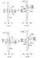
- FIG. 6Ashows an energy band diagrams for a Gated-PFET comprised of an N+ poly Silicon gate material 512 , oxide insulator 505 , and P ⁇ doped channel 506 in FIG. 5A when the gate and channel are both biased to level 600 .
- Reference level 600is at V D volts. This bias condition occurs near the source edge of an off Gated-PFET device with gate and source at V D voltage.
- Levels 601 , 602 and 603represent the conduction band, mid gap band and the valence band energy levels for N+ doped poly Silicon.
- the band gapis about 1.12 eV at 300 Kelvin temperature as shown by the difference between levels 601 and 603 .
- the Fermi levelis at the conduction band level 601 .
- Energy levels 631 , 632 and 634represent the conduction band, mid gap band and the valence band energy levels for P ⁇ channel Silicon. Again the band gap is 1.12 eV for Silicon at 300 Kelvin, shown by the energy difference between 631 and 634 .
- the Fermi level for P ⁇ Siliconis shown by level 633 .
- the P ⁇ Siliconhas a higher vacuum level electron energy compared to N+ poly Silicon. In the diagram, no oxide charge is assumed, and the difference in energy level is the work function difference between the two materials. In the diagram work function difference is assumed to equal flat band voltage. Presence of fixed oxide charge reduces the flat band voltage.
- a thickness 642is shown to be significantly depleted of carriers. That region has no conducting majority carrier holes. Choosing an appropriate Silicon channel height 642 allows building a Gated-PFET channel that does not conduct when a V D voltage is applied on the gate.
- FIG. 6Bis a Gated-PFET energy band diagram when the gate is at V D and the channel at zero or V S volts. This condition can occur at the drain edge of an off Gated-PFET when the drain has to support V S .
- the Silicon Fermi level 6033is at V S while the gate Fermi level 6001 is at V D .
- the two Fermi levels 6033 and 6001are separated by the bias voltage 6061 which has a value V D .
- the depletion region 6040is deeper than 640 , extending to a depth 6041 into the Silicon.
- a thin layer channel that is fully depleted in FIG. 6Aremains filly depleted in FIG. 6B .
- Such a channelhas no conduction between a source and a drain that are biased to V D and V S voltages respectively. Regardless of drain voltage, the Gated-PFET is off when the gate is at V D . This can be seen by the increased band bending shown in FIG. 6B .
- V DAs the gate voltage decrease from V D to a value (V D ⁇ V TP ), the voltage drop across the oxide decreases, and the Silicon depletion width 641 also decreases.
- V TPis chosen such that there is a clear noise margin on the threshold level of the Gated-PFET against power and ground voltage variations.
- the depletion width 641falls to within the film thickness 642 shown in FIG. 6A at the source edge. That creates an onset of conduction current between the source and drain, even if the drain edge is still fully depleted and pinched off. The drain edge pinch off contributes to creating a saturation current.
- V FBThis flat band voltage is defined V FB and is shown by voltage level 761 .
- the gateis biased to V FB while the channel is held at V D .
- Fermi level 733 in the Siliconis at V D
- the Fermi level of N+ polyis at V FB .
- the voltage drop across the oxide 751is zero, and the band bending in the Silicon is also zero.
- V FBequals the work-function difference between gate and Silicon. There is no meaning to a depletion region under this bias condition, and the entire Silicon film thickness 742 has majority carriers at the doping level of the Silicon.
- FIG. 7Bshows the gate at V FB and the channel at drain edge biased to V S .
- Silicon Fermi level 7033is at zero (V S ) volts, while Gate Fermi level 7001 is at V FB .
- Voltage level 7061shows the applied channel voltage V S against reference level 700 at V D .
- the over voltage between V FB and V Sis now dropped across the oxide and the Silicon creating a depletion region 7040 in Silicon.
- Such depletioncauses a current saturation in the conducting channel.
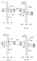
- FIGS. 8A and 8BA Gated-PFET with a gate biased at ground (V S ) is shown in FIGS. 8A and 8B .
- the channel near source edgeis at voltage V D .
- Gate Fermi level 801is at V S
- the channel Fermi level 833is at V D .
- the over voltage between V FB and V Dis now dropped across the oxide and the Silicon creating an accumulation region 840 near the channel surface.
- the majority carrier concentrationis now far higher than the original doping level of the Silicon layer. This provides enhanced channel conduction beyond the doping level chosen for the film.
- the channel film thickness 842is chosen thicker than the accumulation width to facilitate a strong on current for the Gated-PFET.
- FIG. 8Bshows the gate and channel both at V S .
- Both Fermi levels 8001 and 8033are at V S , above reference level 800 by a value V D .
- the band diagramis identical to FIG. 6A when both sides were biased at V D . Again the drain edge of the channel is pinched-off demonstrating the existence of current saturation in the device.
- FIG. 6, 7 and 8have consistent labels. All diagrams consistently show the existence of a thin film channel region that will allow construction of a Gated-PJFET device by ensuring an on state and an off state.
- the channelis fully depleted of majority carriers in the off state.
- the gate and the semiconductor material propertiesneed to be chosen to ensure this condition.
- the flat band voltage for the systemneeds to be large enough to fully deplete the chosen channel thickness when the device is off.
- an N+ doped poly Silicon gate material, an oxide dielectric and a P ⁇ doped Silicon channelmeets that condition.
- a thinner dielectric thickness and a lower dielectric constant material for the gate insulatorallow a lower voltage loss across the dielectric and a larger channel modulation in the Silicon.
- FIG. 9BTop view in FIG. 9B shows a first semiconductor geometry 9080 orthogonal to a gate geometry 9022 . These two layers are separated by an insulator deposited in between.
- the gate geometry 9022is surrounded by a spacer ring 9020 .
- a source voltage 9003is connected via a contact to source region 9013 formed on semiconductor geometry 9080 .
- a drain voltage 9004is connected via a contact to drain region 9014 formed on semiconductor geometry 9080 .
- Geometry 9080is subdivided by implant type into different regions. The separation occurs by overlapping nature of gate geometry 9022 and spacer ring 9020 above geometry 9080 .
- the middle region under gate geometry 9022is defined as the channel region.
- the two regions under the spacer ring 9020are defined as the lightly doped drain (LDN) regions. These regions are better seen in the cross sectional view in FIG. 9A as channel region 906 and LDN regions 984 and 986 .
- LDNlightly doped drain
- the source and drain regions 913 and 914are shown completely salicided with no N+ implanted semiconductor regions. The source and drains are entirely determined by the LDN regions.
- FIG. 9Aalso shows a poly-Silicon gate material 912 partially salicided. Source 913 , drain 914 and gate 912 salicidations occur simultaneously and a thicker poly-Silicon film for gate 912 ensures partial consumption.
- Terminals 902 , 903 and 904are coupled to the regions 912 , 913 and 914 respectively completing a three terminal device. There is no fourth terminal in this device as the channel 906 is electrically coupled between source 913 and drain 914 . There is no body region for this device.
- the channel 906 heightis same as the deposited semiconductor film 9080 thickness.
- Gated-NFETThe operation of Gated-NFET is described next.
- the devicehas an on threshold voltage V TN .
- Gated-NFET source 903is connected to the lower voltage compared to drain 904 .
- Device on-offis determined by gate 902 over voltage with respect to source 903 .
- ground supply voltage V Sis taken as the lower voltage.
- the other voltageis taken as a power supply voltage V D .
- the source terminal 903is assumed connected to the system ground voltage V S .
- the gate voltage 902is between V S and V TN
- the deviceis off with no significant current flow between drain and source.
- the gate voltage 902When the gate voltage 902 is between V TN and V D the device is on.
- the drain to source current flowdepends on the voltage difference between the two terminals V DS .
- FIG. 10Ashows an energy band diagrams for a Gated-NFET comprised of a P+ poly Silicon gate material 1010 , oxide insulator 1020 , and N ⁇ doped channel 1030 when the gate and channel are biased at V S volts at level 1000 .
- This bias conditionoccurs near the source edge of an off device with gate and source at V S voltage.
- Levels 1001 , 1002 and 1003represent the conduction band, mid gap band and the valence band energy levels for P+ poly Silicon.
- the band gapis about 1.12 eV at 300 Kelvin temperature as shown by the difference between levels 1001 and 1003 .
- the Fermi levelis at the valence band level 1003 .
- Energy levels 1031 , 1033 and 1034represent the conduction band, mid gap band and the valence band energy levels for P ⁇ channel Silicon. Again the band gap is 1.12 eV for Silicon at 300 Kelvin, shown by the energy difference between 1031 and 1034 .
- the Fermi level for N ⁇ Siliconis shown by level 1032 .
- the N ⁇ Siliconhas a lower vacuum level electron energy compared to P+ poly Silicon. In the diagram, no oxide charge is assumed, and the difference in energy level is the work function difference between the two materials. There is a net electron transfer from Gate side to the Silicon side causing band bending as shown in FIG. 10A . This creates voltage drop across the oxide and Silicon according to the laws of Semiconductor Physics.
- the voltage drop in the oxideis shown by the difference 1051 with a uniform electric field in the absence of fixed charge inside the oxide.
- the voltage drop inside Siliconcreates a band bending region 1040 with a depth 1041 into Silicon from the oxide interface. This region is depleted of majority carrier electrons. There is no supply of minority carriers (a P type diffusion region) to cause a surface inversion layer and pin the band bending at the surface as shown by region 110 in FIG. 1 for a MOSFET device.
- a thickness 1042is shown to be significantly depleted of carriers near the surface. That region has no conducting majority carrier electrons. Choosing an appropriate Silicon channel height 1042 allows constructing a Gated-NFET channel that does not conduct when a V S voltage is applied on the gate.
- FIG. 10Bis a Gated-NFET energy band diagram when the gate is at V S and the channel at V D volts. This can occur at the drain edge of an off Gated-NFET when the drain has to support a voltage V D .
- the Silicon Fermi level 10032is at V D while the gate Fermi level 10003 is at V S .
- the two Fermi levels 10032 and 10003are separated by the bias voltage 10061 which has a value V D .
- the depletion region 10040is deeper than 1040 , extending to a depth 10041 into the Silicon. A thin layer channel that is filly depleted in FIG. 10 A remains fully depleted in FIG. 10B .
- Such a channelhas no conduction between a source and a drain that are biased to V S and V D voltages respectively. Regardless of drain voltage, the Gated-NFET is off when the gate is at V S . This can be seen by the enhanced band bending shown in FIG. 10B .
- V TNis chosen such that there is a clear noise margin on the threshold level of the Gated-NFET against power and ground voltage variations.
- the depletion width 1041falls to within the film thickness 1042 shown in FIG. 10A at the source edge. That creates an onset of conduction current between the source and drain, even if the drain edge is still fully depleted and pinched off. The drain edge pinch off contributes to creating a saturation current.
- V FBThis flat band voltage is defined V FB and is shown by voltage level 1161 .
- Fixed oxide chargeaffect V FB .
- the gateis biased to V FB while the channel is held at V S .
- Fermi level 1132 in the Siliconis at V S
- the Fermi level of P+ poly 1103is at V FB .
- the voltage drop across the oxide 1151is zero, and the band bending in the Silicon is also zero.
- V FBequals the work-function difference between gate and Silicon.
- FIG. 11Bshows the gate at V FB and the channel at drain edge biased to V D .
- Silicon Fermi level 11032is at V D volts
- Gate Fermi level 11003is at V FB .
- Voltage level 11061shows the applied channel voltage V D against reference level 1100 at V S .
- the over voltage between V FB and V Dis now dropped across the oxide and the Silicon creating a depletion region 11040 in Silicon.
- Such depletioncauses a current saturation in the conducting channel.
- FIG. 12A and 12BA Gated-NFET with a gate biased at power supply V D is shown in FIG. 12A and 12B .
- the channelis at source edge with a voltage V S .
- Gate Fermi level 1203is at V D
- the channel Fermi level 1232is at V S .
- the over voltage between V FB and V Dis now dropped across the oxide and the Silicon creating an accumulation region 1240 near the channel surface.
- the majority carrier concentrationis now far higher than the original doping level of the Silicon layer. This provides enhanced channel conduction beyond the doping level chosen for the film.
- the channel film thickness 1242is chosen thicker than the accumulation width to facilitate a strong on current for the Gated-NFET.
- FIG. 12Bshows the gate and channel both at V D .
- Both Fermi levels 12003 and 12032are at V D , above reference level 1200 by a value V D .
- the band diagramis identical to FIG. 10A when both sides were biased at V S . Again the drain edge of the channel is pinched-off demonstrating the existence of current saturation in the device.
- FIGS. 10, 11 and 12have consistent labels. All diagrams consistently show the existence of a thin film channel region that will allow construction of a Gated-NJFET device by ensuring an on state and an off state. The channel is fully depleted of majority carriers in the off state. The gate and the semiconductor material properties need to be chosen to ensure this condition. The flat band voltage for the system needs to be large enough to fully deplete the chosen channel thickness when the device is off. In the embodiment chosen a P+ doped poly Silicon gate material, an oxide dielectric and an N ⁇ doped Silicon channel meets that condition. A thinner dielectric thickness and a lower dielectric constant material for the gate insulator allow a lower voltage loss across the dielectric and a larger channel modulation in the Silicon.
- the lightly doped resistive channel region formed on a first semiconductor thin film geometry 480 forming the conducting paths between source 413 and drain 414 in FIG. 4can be a thinned down SOI single crystal Silicon film, or a deposited thin Poly-crystaline Silicon film, or a post laser annealed as deposited amorphous Poly-crystalline Silicon film.
- the thickness and doping of the channel region 406are optimized with the insulator 405 thickness T G and gate material work function to get the required threshold voltage Vt, on-current and off-current for these devices.
- X⁇ S *T G /F G Angstroms
- Y[(2* ⁇ S *V FB )/( q*D )] 0.5 Angstroms
- X D( X 2 +Y 2 ) 0.5 ⁇ X Angstroms (EQ 3) T S ⁇ X D Angstroms (EQ 4)
- ⁇ Schannel semiconductor permittivity
- ⁇ Ggate insulator permittivity
- T Ggate insulator thickness
- V FBgate to semiconductor absolute flat band voltage
- qelectron charge
- Dchannel doping level
- X Dis the depletion depth
- T Schannel semiconductor layer thickness.
- EQ-3denotes the maximum depletion width for the off Gated-FET shown as depth 641 in FIG. 6A and depth 1041 in FIG. 10A .
- the inequality in EQ-4ensures film thicknesses 642 and 1042 shown FIGS. 6A and 10A respectively are within the maximum depletion depths 641 and 1041 into Silicon channel.
- T Sis chosen to be in the range 0.2*X D to 0.9*X D , and more preferably T S is chosen to be in the range 0.4*X D to 0.8*X D range.
- X DY ⁇ X+X 2 /(2 *Y ) Angstroms (EQ 5)
- the insulator thickness and channel dopingalso needs to satisfy the threshold voltage for the Gated-FET device.
- This threshold voltageis preferable selected in the range 0.18*V D to 0.4*V D , and more preferably 0.2*V D to 0.3*V D , where V D is the power supply voltage. This puts an added constraint on the semiconductor film thickness 642 and 1042 shown in FIG. 6A and FIG. 10A respectively.
- V Tis applied at the gate
- the depletion width 641 (or 1041 )equals semiconductor thickness 642 (or 1042 ) for the Gated-FET device.
- T S( X 2 +Z 2 ) 0.5 ⁇ X Angstroms (EQ 8)
- EQ-8shows the relationship between doping level D and semiconductor film thickness T S required to satisfy the Gated-FET design.
- EQ-8satisfies the constraint for maximum semiconductor film thickness in EQ-4 trivially.
- the gate dielectric thickness and dielectric fixed charge densityimpacts this threshold voltage.
- Gate dielectricscan be oxide, oxy-nitride, nitride, or multi-layered insulators.
- the semiconductor materialmay be Silicon, Silicon-germanium, gallium-arsenide, germanium, or any other III-V material.
- the gate materialmay be poly-Silicon, aluminum, tungsten, or any other metal. The value of X in equation-1 will change based on the physical properties of the materials chosen to form the Gated-FET device.
- the total resistance of the conducting body region for Gated-FET under conducting modeis determined by the applied voltage difference between drain and source nodes, and gate over voltage above threshold.
- a typical device top view and cross sectionis shown in FIG. 13 .
- the device channel width 1391 (W S ), device channel length 1392 (L S ) and film thickness 1393 (T S )all determine the device on current.
- Gate voltage and channel depletion heavily modulates resistivity ps Parametersare chosen for R to be preferably in the 1 KOhm to 1 Meg-Ohm range, more preferably 10 KOhm to 100 KOhms, when the channel is on.
- the resistivity for single crystal Siliconis 0.12 Ohm-cm.
- L S0.3 ⁇
- W S0.3 ⁇
- T S431 Angstroms
- Ris 27.8 KOhms.
- V DS0.2V (drain to source bias)
- the channel current I ONis 7 ⁇ A. This is the conduction level under flat band bias condition in FIG. 7A for the Gated-PFET.
- Poly-Silicon mobilityis lower than single crystal Silicon degrading the on current for non single-crystal films.
- the surface accumulations shown in FIG. 8A and FIG. 12A for Gated-PFET and Gated-NFET devicesenhance the channel I ON current for higher gate biases.
- ⁇absorbs the channel modulation effects
- ⁇ S0remains the resistivity at doping level D of the thin film channel region.
- the ⁇ valuedepends on the depth of the accumulation region into thin film channel, and the surface potential at the Semiconductor-Insulator interface in the band diagrams in FIG. 8A and FIG. 12 -A If the absolute surface potential is ⁇ S in the semiconductor, a system of equations can be solved by trial and error to converge on the correct ⁇ S value.
- N SD *exp( q ⁇ S /kT ) (EQ 11)
- L D[ ⁇ S *kT /( q 2 N S )] 0.5
- X A⁇ square root ⁇ 2 *L D *[( N S /D ) 0.5 ⁇ 1]
- Q Sq*N S *X A /(1+ X A /( ⁇ square root ⁇ 2 *L D )] (EQ 14)
- ⁇ SV D ⁇ V FB ⁇ T G *Q S / ⁇ G (EQ 15)
- EQ-11denotes the excess surface concentration of majority carriers due to the surface potential ⁇ S at the surface.
- EQ-12denotes the Debye length at the surface concentration N S .
- EQ-13denotes the depth of accumulation layer penetration into semiconductor region. At this depth, the doping level drops off to the channel doping level D, and no accumulation is further observed.
- EQ-14denotes the total excess accumulation charge in the semiconductor thin film due to accumulation.
- EQ-15is the voltage balance where the over voltage above flat-band is distributed across gate insulator and semiconductor film. A consistent solution to the system of equations 11-15 can be achieved iteratively. To achieve the full benefit from the enhanced conduction due to accumulation, the film thickness is further chosen such that: T S >X A (EQ 16)
- T Sis chosen in the range 1*X A to 10*X A , and more preferably T S is chosen in the range 2*X A to 6*X A .
- the device shown in FIG. 13has P+ doped poly-Silicon gate over N ⁇ doped channel for the Gated-NFET, and N+ doped poly-Silicon gate over P ⁇ doped channel for the Gated-PFET. This is easily achieved in the fully salicided source/drain embodiment shown in FIG. 13 .
- the Gated-NFET and Gated-PFET gate regions 1312are first doped P+ and N+ respectively before the gates are etched. After gates are etched, prior to spacer 1320 formation, Gated-NFETs are implanted with N type LDN tip implant and Gated-PFETs are implanted with P type LDP tip implant.
- the LDD tip-implant doseis much lower than the gate doping to affect gate doping type.
- the Source & Drain regionsare now defined by the self aligned LDD tip implants regions 1326 shown under the spacer oxides 1320 adjacent to the gate 1312 regions in FIG. 13B . As the drain 1314 and source 1313 regions outside the spacer are fully consumed by salicide, those regions do not need heavy doping.
- the channel 1306 doping levels N ⁇ for Gated-NFET and P ⁇ for Gated-PFETare chosen to achieve the desirable VT as discussed earlier.
- the first semiconductor thin film layer 1306 forming the source 1313 , LDD tips 1326 , channel 1306 and drain 1314can be thinned down SOI single crystal Silicon material, or a first thin-film PolySilicon layer, or a laser crystallized amorphous Silicon layer, or any other thin film semiconductor layer. A thicker first film allows higher current.
- the gate dielectric 1305is grown either thermally or deposited by PECVD.
- the first thin film layer 1306 (P 1 )forms the body of the transistor.
- the P 1 layeris deposited above the insulator layer 1307 .
- the insulatoris oxide, or nitride, or a reversed bias doped semiconductor region (in the case when source and drain regions are not fully salicided) that can isolate P 1 geometry 1380 .
- a P 1 maskis used to define and etch these P 1 islands. Gated-PFET regions are mask selected and implanted with P ⁇ doping, and gated N-FET devices are implanted with N ⁇ doping, the channel doping V T levels required for Gated-FET devices.
- the gate 1312is deposited after the gate insulator 1305 is deposited as a second thin film semiconductor layer (P 2 ).
- the second thin film layeris a PolySilicon layer.
- the Gated-PFET gate poly 1312is mask selected and implanted N+ and Gated-NFET is implanted with P+ prior to gate definition and etch. The gate regions are then defined and etched.
- a P tip (LDP) implantis used over all Gated-PFET devices, and an N tip (LDN) implant is used for Gated-NFET devices. This can be done by open selecting Gated-PFET devices, and not selecting Gated-NFET devices and visa-versa.
- the N+ and P+ doped gatesare not affected by the lower N and P tip implant level.
- Gate 1312blocks P and N tip implants getting into channel region 1340 , and only P 1 regions outside P 2 gets this tip implant.
- Spacer oxide regions 1320are formed on either side of gate by conventional oxide deposition and etch back techniques.
- the P 2 gate 1312is perpendicular to P 1 geometry 1380 .
- the n gate 1312 and spacers 1320sub-divide the P 1 geometry into five regions: (1) source region 1313 , (2) source spacer region 1326 doped with LDD tip implant, (3) channel region 1306 doped with V T implant, (4) drain spacer region 1326 also doped with LDD tip implant and (5) drain region 1314 .
- the source and drain regionsare fully salicided and need no implant.
- a dielectric film 1370is deposited and C 2 1375 is defined and etched. These are W-filled and polished.
- a M 1 1380is deposited, defined and etched, and a dielectric 1390 deposited to add multiple layers of metal in the process.
- P 1refers to the first semiconductor layer in FIG. 13 and P 2 refers to the second semiconductor layer in FIG. 13 forming the gate.
- An ideal filmis a single crystal Silicon with a precise thickness control over an insulator. In SOI technology, the single crystal Silicon layer above an insulator meets this criterion.
- P 1is mask selected and thinned down to the required thickness as defined by EQ-8. This allows formation of two sets of transistors adjacent to each other: regular SOI MOSFET and thinned down SOI Gated-FET.
- a logic processis used to fabricate CMOS devices on a substrate layer. These CMOS devices may be used to build AND gates, OR gates, inverters, adders, multipliers, memory and other logic functions in an integrated circuit.
- a Complementary Gated-FET TFT module layeris inserted to a logic process at a first contact mask to build a second set of TFT Gated-FET devices.
- An exemplary logic processmay include one or more following steps:
- FIG. 14shows an exemplary process for fabricating a thin film Gated-FET device in a module layer.
- the process in FIG. 14forms a Gated-FET device in a layer substantially above the substrate layer.
- the processing sequence in FIG. 14 . 1 through 14 . 8describes the physical construction of a Gated-FET device shown in FIG. 13 .
- the process shown in FIG. 14includes adding one or more following steps to the logic process after ILD oxide CMP step.
- the TFT process technologyconsists of creating Gated-PFET and Gated-NFET poly-Silicon transistors.
- the module insertionis after the substrate device gate poly etch and the ILD film deposition.
- the insertion pointmay be after M 1 and the subsequent ILD deposition, prior to V 1 mask, or between two other metal definition steps.
- the polyis salicided using Cobalt or Nickel & RTA sequences. Then an ILD is deposited, and polished by CMP techniques to a desired thickness.
- the contact maskis split into two levels. The first C 1 mask contains all contacts that connect Gated-FET outputs to substrate transistor gates or diffusion nodes. Then the C 1 mask is used to open and etch contacts in the ILD film. Ti/TiN glue layer followed by W-Six plugs, W plugs or Si plugs may be used to fill the plugs, then CMP polished to leave the fill material only in the contact holes. The choice of fill material is based on the thermal requirements of the TFT module in subsequent steps. Si plugs allow RTA thermal oxidation of P 1 at a subsequent step.
- a first P 1 poly layeramorphous or crystalline, is deposited by LPCVD to a desired thickness as shown in FIG. 14 . 1 .
- the P 1 thicknessis between 50 A and 1000 A, and preferably between 200-600 A.
- This poly layer P 1is used for the channel, source, and drain regions for both Gated-FETs.
- P 1is patterned and etched to form the transistor geometries. In other embodiments, P 1 is used as contact pedestals to stack a C 2 contact above C 1 .
- Gated-NFET transistorsare blanket implanted with N ⁇ doping, while the Gated-PFET transistor regions are mask selected and implanted with P ⁇ doping. This is shown in FIG. 14 . 2 .
- the implant doses and P 1 thicknessare optimized to get the required threshold voltages for Gated-PFET & Gated-NFET devices under fully depleted transistor operation, and maximize on/off device current ratio.
- the pedestals implant typeis irrelevant at this point.
- the V T implantationis done with a mask P ⁇ implant followed by masked N ⁇ implant.
- First dopingcan also be done in-situ during poly deposition or by blanket implant after poly is deposited.
- Patterned and implanted P 1may be subjected to dopant activation and crystallization.
- RTA cycleis used to activate & crystallize the poly after it is patterned to near single crystal form.
- the gate dielectricis deposited, and buried contact mask is used to etch areas where P 1 contacts P 2 layer.
- Niis deposited and salicided with RTA cycle. All of the P 1 in contact with Ni is salicided, while the rest poly is crystallized to near single crystal form. Then the unreacted Ni is etched away.
- amorphous polyis crystallized prior to P 1 patterning with an oxide cap, metal seed mask, Ni deposition and MILC (Metal-Induced-Lateral-Crystallization).
- the TFT gate dielectric layeris deposited followed by P 2 layer deposition.
- the dielectricis deposited by PECVD techniques to a desired thickness in the 30-200 A range, desirably 30-100 A thick.
- the gatemay be grown thermally by using RTA when C 1 plug fill is doped Silicon.
- This gate materialcould be an oxide, nitride, oxynitride, ONO structure, or any other dielectric material combination used as gate dielectric.
- the dielectric thicknessis determined by the voltage level of the process.
- an optional buried contact mask BCmay be used to open selected P 1 contact regions, etch the dielectric and expose P 1 layer. BC could be used on P 1 pedestals to form P 1 /P 2 stacks over C 1 .
- the dielectric deposition and buried contact etchoccur before the crystallization. In the preferred embodiment, no BC is used.
- second poly P 2 layer200 A to 1000 A thick, preferably 300-800 A is deposited as amorphous or crystalline poly-Silicon by LPCVD as shown in FIG. 14 . 3 .
- Gated-NFET devices & P+ poly interconnectsare blanket implanted with P+ implant. The implant energy ensures full dopant penetration into the P 2 layer. This doping gets to only P 2 regions as no P 1 regions are exposed.
- An N+ maskis used to select Gated-PFET devices and N+ interconnect, and implanted with N+ dopant as shown in FIG. 14 . 4 .
- Transistor gate regions of Gated-PFET and Gated-NFETare doped to the correct dopant type.
- Source and drain regionsare blocked by P 1 and not implanted. This N+/P+ implants can be done with N+ mask followed by P+ mask. The V T implanted P 1 regions are completely covered by P 2 layer and form channel regions of Gated-NFET & Gated-PFET transistors.
- P 2 layeris defined into Gated-NFET & Gated-PFET gate regions intersecting the P 1 layer channel regions, C 1 pedestals if needed, and local interconnect lines and then etched as shown in FIG. 14 . 5 .
- the P 2 layer etchingis continued until the dielectric oxide is exposed over P 1 areas uncovered by P 2 (source, drain, P 1 resistors).
- the source & drain P 1 regions orthogonal to P 2 gate regionsare now self aligned to P 2 gate edges.
- the S/D P 2 regionsmay contact P 1 via buried contacts.
- Gated-NFET devicesare blanket implanted with LDN N dopant. Then Gated-PFET devices are mask selected and implanted with LDP P dopant as shown in FIG.
- the implant energyensures full dopant penetration through the residual oxide into the S/D regions adjacent to P 2 layers.
- the N and P type dopant levelis much lower than the N+ and P+ dopant levels used to dope P 2 regions. Hence P 2 is unaffected by these LDD implants.
- a spacer oxideis deposited over the LDD implanted P 2 using LTO or PECV D techniques as shown in FIG. 14 . 6 .
- the oxideis etched to form spacers 1320 shown in FIG. 13 .
- the spacer etchleaves a residual oxide over P 1 in a first embodiment, and completely removes oxide over exposed P 1 in a second embodiment. The latter allows for P 1 salicidation at a subsequent step.
- Nickelis deposited over P 2 and salicided to form a low resistive refractory metal on exposed poly by RTA. Un-reacted Ni is etched as shown in FIG. 14 . 7 .
- Ni-salicideconnects the opposite doped poly-2 and poly-1 regions together providing low resistive poly wires for data transfer.
- the residual gate dielectric left after the spacerprevents P 1 layer salicidation.
- P 1is salicided.
- the thickness of Ni depositionmay be used to control full or partial salicidation of P 1 regions in FIG. 13 . Fully salicided S/D regions up to spacer edge facilitate high drive current due to lower source and drain resistances.
- An LTO filmis deposited over P 2 layer, and polished flat with CMP.
- a second contact mask C 2is used to open contacts into the TFT P 2 and P 1 regions in addition to all other contacts to substrate transistors.
- C 1 contacts connecting Gated-FET outputs to substrate transistorsrequire no C 2 contacts.
- Contact plugsare covered with a glue layer, filled with tungsten, CMP polished, and connected by metal as done in standard contact metallization of IC's as shown in FIG. 14 . 8 .
- thinned down SOIis used to construct the Gated-FET shown in FIG. 13 .
- the SOI starting waferis chosen to have the correct P 1 thickness as given by EQ-8. This can be achieved by thinning down an existing SOI wafer to Silicon thickness ⁇ 400 A as discussed in the example.
- the process sequenceis similar to the Gated-FET TFT device fabrication, except for the starting point. There is no preceding logic process, and the P 1 definition is the starting point for the Gated device fabrication as detailed in the TFT process sequence.
- an SOI logic processis used to fabricate CMOS devices on a substrate layer, and a second thinned down Gated-FET device for special applications.
- Standard SOI devicesmay be used to build AND gates, OR gates, inverters, adders, multipliers, memory and other logic functions in an integrated circuit
- Thinned down SOI Gated-FET devicesmay be constructed to integrate a high density of latches or memory into the first fabrication module.
- a thinned down SOI moduleis inserted to an exemplary SOI logic process which includes one or more of following steps:
- the Gated-FET body dopingis independently optimized for performance, but shares the same LDN, LDP implants.
- the Gated-FET gatesare separately doped N+ & P+ prior to gate etch and blocked during N+/P+ implants of peripheral SOI devices as the dopant types differ.
- Gated-FET devices and periphery MOSFET devicesmay share one or more V T implants.
- One P 2is used for latch and peripheral device gates.
- SOI substrate devicesmay be integrated with a TFT latch module. This allows for a SOI inverter and TFT inverter to be vertically integrated to build high density, fast access memory devices.
- FPGAfield programmable gate array
- ASICapplication specific integrated circuit
- Multiple ASICscan be fabricated with different variations of conductive patterns from the same FPGA.
- the memory circuit and the conductive patterncontain one or more substantially matching circuit characteristics.
- the processcan be used to fabricate a high density generic static random access memory (SRAM) with inverters connecting to form latches and SRAM memory.
- SRAMstatic random access memory
- a TFT modulemay be used to build a vertically integrated SRAM cell with one inverter on a substrate layer, and a second inverter in a TFT layer.
Landscapes
- Thin Film Transistor (AREA)
Abstract
Description
- This application is a division of application Ser. No. 10/62,627 filed on Jan. 23, 2004, which is a division of application Ser. No. 10/413,808 filed on Apr. 14, 2003, which claims benefit from Provisional Application Ser. No. 60/393,763 filed on Jul. 08, 2002, Provisional Application Ser. No. 60/397,070 filed on Jul. 22, 2002, Provisional Application Ser. No. 60/400,007 filed on Aug. 01, 2002, Provisional Application Ser. No. 60/402,573 filed on Aug. 12, 2002, and Provisional Application Ser. No. 60/449,011 filed on Feb. 24, 2003, all of which list as inventor Mr. R. U. Madurawe and the contents of which are incorporated-by-reference.
- This application is also related to application Ser. No. 10/267,484, Application Ser. No. 10/267,483, and application Ser. No. 10/267,511 now U.S. Pat. No. 6,747,478, all of which were filed on Oct. 08, 2002 and list as inventor Mr. R. U. Madurawe, the contents of which are incorporated-by-reference.
- The present invention relates to semiconductor IGFET devices.
- An Insulated-Gate Field-Effect Transistor, or IGFET, is a device of very major importance in the semiconductor IC industry. A Metal-Oxide-Silicon Field-Effect Transistor, or MOSFET, is a sub-class of IGFET devices. An IGFET is a four terminal device comprising of a source, drain, gate and body nodes; though the body node only allows very limited access to the device. MOSFETs are widely used in the sub micron semiconductor processing technologies to manufacture Ultra Large Scale Integrated Circuits. Ability to form Silicon-oxide interfaces with very low interface states, quality gate oxides with low thickness, reductions in system voltage and reductions in lateral geometries by lithography improvements have all contributed to the popularity of these transistors. Today MOSFETs are used to build ASICs, Memory, FPGA, Gate Array, Graphics, Micro Processors, and a wide variety of semiconductor IC products.
- IGFET differ from a Bipolar Transistor in the power level and power amplification available in the device. Bipolar transistor is a three terminal device with a base, an emitter and a collector node. Compared to the base control terminal of a Bipolar traitor, the gate control terminal of IGFET consumes essentially no power. While the Bipolar can deliver more output power, the gain (defined by the ratio of output current to control current) is infinite for IGFET compared to about 500 for a good Bipolar transistor. This high gain coupled with complementary MOSFET design methodology facilitates low stand-by power in ICs that have over 10 Million transistors. Bipolar is used to build many Analog and Linear ICs such as voltage regulators, power amplifiers, rectifiers, battery regulators, D to A Converters and A to D Converters due to the high output power available. Sub-micron geometry MOSFETs with high current drives are now increasingly used for similar applications.
- IGFET differs from a JFET, also a three terminal device, in the construction of the transistor. In the IGFET the gate is insulated above the transistor body, while in the JFET the gate is formed as a reverse biased junction above the conducting channel. The reverse bias control gate junction consumes a low level of power due to carrier recombination inside the depleted region. The JFET power amplification is better than a Bipolar, but lower than an IGFET. A significant difference between IGFET and JFET occurs in the method of channel conduction. This will be discussed in detail next.
- The MOSFET operates by conducting current between its drain and source through a conducting inversion layer created by the presence of a gate voltage.
FIG. 1 shows a cross section of a MOSFET device, and is described herein with reference to an NMOSFET device. InFIG. 1 , anNMOS transistor body 100 is P− doped, isolating an N+ dopedsource region 113 and an N+ doped drain region114. The source is connected to afirst voltage 103, which may be the ground supply VS. The drain is connected to asecond voltage 104, which may be a switching voltage node for the device. The body region between source and drain under thegate 112 is also doped P type same as substrate. The result is the formation of two N+/P− back-to-back reverse-biased diodes. When thevoltage 102 atgate 112 is zero, or below a threshold voltage VTN, the N+/P− back-to-back reverse-biased diodes do not conduct and the transistor is off. The surface undergate 112 consists of hole carriers. In the embodiment ofFIG. 1 , thegate 112 includes a salicided region shown shaded, and the source and drain salicidation is not shown. When the gate voltage is greater than a threshold voltage (VTN), aninversion 110 occurs undergate 112. This inversion layer, called a conducting channel, completes an electron carrier path between thesource 103 and drain104 regions. For the MOSFET inFIG. 1 , the terminology inversion layer and conducting channel is used interchangeably, and is shown by110. This conducting channel facilitates current flow betweensource 113 and drain114 regions. Hole carrier depletion occurs adjacent to thebody region 100 under theinversion layer 110 and adjacent tosource 113 and drain114 regions. This is shown shaded inFIG. 1 . This charge is due to the reversed bias electric fields from the gate, source and drain voltages. The component of this depleted charge from the gate voltage determines the magnitude of the VTN. Trapped oxide charge and Silicon defects affect the VTNtransistor parameter. The more positive the voltage is at the gate, the stronger is the inversion layer charge and hence the channel conduction. At all levels, thesubstrate 100 potential is kept at the lowest voltage level. In most applications, the substrate and source are held at VS. For special applications, the NMOS body can be pumped to a negative voltage. - A PMOS device is analogous to an NMOS device, with the device operational polarity and doping types reversed. A PMOS is on when the gate is in the voltage range from system ground VSto a threshold difference (VD−VTP), and off when the gate is in the voltage range (VD−VTP) to system power voltage VD. Channel conduction is between P+ doped source and P+ doped drain, via a surface inversion P− layer. The body region originally doped N− gets depleted by the gate potential. The body region for a PMOS is termed Nwell and is constructed on a P type substrate wafer as an isolated island. The Nwell is biased to the highest PMOS device potential, and in most applications the source and Nwell are held at VD. For special applications, the PMOS body can be pumped to a voltage higher than the power supply voltage.
- In a MOSFET device, there is a
body region 100 under the gate. In fact, a conducting channel is not formed until the surface is in inversion with a build up of minority carriers The gate depletes the body region near the surface to create this inversion layer at the surface. The depletion width reaches a maximum depth at the onset of inversion, and stays constant at higher gate biases. As the body extends well into the bottom surface of the substrate, the gate modulation has little impact on the resistance of the body region between the source and drain regions. A special case of a MOSFET is a depletion device. In the NMOS depletion device, an N− implanted channel is formed under the gate on the device body surface between N+ source and N+ drain regions. This depletion device has a negative threshold voltage, and a negative gate voltage is needed to turn the device off. The channel is modulated by two terminals: the gate above the oxide, and the body below the channel. The body below has a significant impact on the channel resistance, and in some depletion devices a negative body bias is needed to turn the depletion device off completely. - As discussed in U.S. Pat. No. 5,537,078, conventional JFET transistors are of two main types: P-channel (PJFET) and N-channel (NJFET).
FIG. 2 shows a cross section of a JFET device. The description that follows is for an NJFET device. InFIG. 2 , asemiconductor channel 206 which has been doped N− is positioned between twoN+ diffusions terminals channel 206 there are two gates which are referred to as thetop gate 212 and thebottom gate 222. Top gate is connected toterminal 202, and the bottom gate is connected to terminal232. In some embodiments, the twogate terminals 202 and232 may be common. Each gate is doped with P+ type dopant to create two back to back P+/N− diodes perpendicular to the channel. When drain and source voltages are different, the drain to source current passes entirely through the conducting N−channel 206. This current increases with higher voltage drop between the terminals, reaching a saturation value at high biases. At saturation, the depletion regions meet at a pinch-off point 230 near the drain edge as shown inFIG. 2 . The gates are biased to keep the gate to channel P+/N− junctions reversed biased. The reversed biased voltage createsdepletion regions 210 and220 that penetrate into the channel reducing the channel height available for current flow. The gate voltages also control the flow of current between the source and drain by modulating the channel height. When the gate reverse bias is sufficiently large, the entire channel is pinched-off causing no current flow between drain and source. In on and off states, there is no current flow through the gate terminal of a JFET due to reverse bias junction voltages, except for junction leakage current. For the device inFIG. 2 a negative gate voltage (lower than VS) creates the channel off condition. Such a negative gate voltage increases the operating voltage of this process, a draw back for JFET scheme. - A PJFET device is analogous to an NJFET device, with the device operational polarity and doping types reversed. A PJFET is on when the gate is at VD, and off when the gate is more positive than VDfurther increasing the voltage level of the process. Channel conduction is between P+ doped source and drain regions via a P− doped channel sandwiched between two N+ doped gate regions. For source and drain terminals at voltages in the range from VSto VD, operating range of NJFET gate is less than VSto VS, while the operating range for PJFET gate is VDto more than VD.
- Compared to the
non-conducting body 100 of MOSFET onFIG. 1 , the JFET has a conductingchannel 206 between source and drain. Due to non-overlapping gate voltages and the high voltage range thus needed, a complementary JFET process is impractical to realize. Hence there is no low cost process that provides CJFET devices analogous to CMOS devices. Compared to the MOSFET inFIG. 1 , a JFET conducting channel is formed inside the body of the switching device. This channel current is not affected by trapped oxide charges near the gate, a draw back with MOSFETs. Compared to MOSFETs, JFETs also have poorer switching characteristics due to higher depleted charge stored in the channel and the transient times required to store and remove this depletion charge. Reverse biased junctions hurt JFET device ease of use and popularity in modern day ICs. - A special MOSFET device constructed in Silicon-on-Insulator (SOI) is shown in
FIG. 3 . This three terminal device is constructed as either an NMOSFET or a PMOSFET. The difference inFIG. 1 andFIG. 3 is in the thickness of thebody region 306 of the device, and in its body isolation. In the SOI device, theregions substrate 300 is isolated from the device region byinsulator 307, hence there is no fourth terminal to this device. This isolation helps with lower junction capacitance and no body effect for SOI MOSFET.Source 313, drain314,gate 312,spacer 320, andsalicided regions FIG. 1 . Two conditions differ in SOI MOSFET when the device in on. In PD SOI, thebody 306 is only partially depleted (PD) when the body is thicker than a maximum depletion width Then a neutral floating body exists insideregion 306 causing deleterious effects on device performance. For thinner FD SOI devices the body is fully depleted (FD) and a neutral body region does not occur. These tend to show short channel effects from the drain and source reverse biased depletions into body region. - Analogous to standard MOSFET, SOI MOSFET also has a non-conducting body under the
gate 312. Thechannel 310 is only formed by inverting the surface. Thebody 306 is fully isolated with no access points. The gate modulation of the body has no influence to access ports. Unlike the body, the conducting channel can be accessed via source and drain nodes. There is no analogous device to depletion MOSFET in SOI. This is due to the floating body in an SOI and the inability to control body voltage. Depletion device behavior strongly depends on the body voltage control. - In one aspect, a semiconductor Gated-FET device comprises of a lightly doped resistive channel region formed on a first semiconductor thin film layer; and an insulator layer deposited on said channel surface with a gate region formed on a gate material deposited on said insulator layer; said gate region receiving a gate voltage having a first level modulating said channel resistance to a substantially non-conductive state and a second level modulating said channel resistance to a substantially conductive state.
- In a second aspect said channel region is formed between a source region and a drain region in the said first semiconductor thin film; and said source region coupled to a source voltage; and said drain region coupled to a drain voltage; and said source and drain regions having a higher level of the same dopant type as said channel region.
- In a third aspect, the Gated-FET device further comprises of an off state with said gate voltage below a first threshold voltage level, and said thin film channel substantially not conducting a current between said drain and source regions for a differential bias voltage ranging from zero to a system power supply voltage; and an on state with said gate voltage above a first threshold voltage level, and said thin film channel substantially conducting a current between said drain and source regions for a differential bias voltage ranging from zero to a system power supply voltage.
- The Gated-FET device is a subset of IGFET devices where the gate is insulated from the channel. This terminology is used to distinguish the new device from MOSFET and JFET devices. A Gated-FET device is a hybrid device between an SOI MOSFET device and a conventional JFET device. The Gated-FET device has a channel region like that of the JFET device: entirely comprising of a thin film resistive channel between its source and drain regions. There is no inversion layer like in an SOI MOSFET to conduct current with no floating body. The gate node of the Gated-FET device is like that of a MOSFET device: the gate constructed above a dielectric material insulating gate from the channel. There is no reverse biased gate junction like in a JFET. The gate voltage thus modulates the channel through the oxide similar to the gate modulation of the SOI MOSFET body region. Unlike in the SOI MOSFET, this modulation occurs in the channel region, which connects the source and drain regions.
- Advantages of the invention may include one or more of the following. A Gated-FET device is used with no increase in voltage range compared to JFET. A Gated-FET device has a threshold voltage not degraded by fixed charge and surface states. A Gated-FET has a channel conductance not degraded by lower surface mobility. A Gated-FET channel current is better controlled with thin film physical properties such as thickness, doping and work function. A Gated-FET has lower charge storage in the channel and faster switching speeds. A Gated-FET has only one gate. A Gated-FET has very low junction capacitance and no body effect. A Gated-FET has no isolated body and no charge trapping effects. A Gated-FET is constructed in a second semiconductor plane, different from a first plane used for logic transistor construction. A Gated-NFET and a Gated-PFET is built on the same process. Gated-FETs are used to build 3D dense integrated circuits. Complementary Gated-FET devices are fabricated in conjunction with regular CMOS devices in a single process. A Gated-NFET and Gated-PFET share a common drain node on a single geometry. The CGated-FETs share a common gate voltage. A switching device is built as a CGated-FET inverter. The CGated-FET inverter has identical gate voltage range as power supply voltage. A latch is constructed with two CGated-FET inverters connected back to back.
- An off-state Gated-FET thin film transistor body is filly depleted. The depleted channel resistance is non-conductive with no current flow between source and drain. An on-state Gated-FET has a surface accumulation. The accumulation enhances the channel conduction beyond the original dopant level. The enhanced Gated-FET channel conduction is 2 to 100 times more than the intrinsic channel conductance. Thin film Gated-FET has superior device on and off characteristics.
- The method of fabricating the Gated-FET may have one or more of following advantages. A Gated-FET is constructed with Ill-V semiconductor material. A Gated-FET is constructed with poly-crystalline semiconductor thin film transistors. A Gated-FET is constructed with amorphous poly-Silicon semiconductor thin film transistors. A Gated-FET is constructed with laser re-crystallized poly-Silicon semiconductor thin film transistors. A Gated-FET is constructed on SOI material, or thinned down region of SOI material. A thinned down crystalline SOI Gated-FET has very high performance. The Gated-FET is fabricated in poly-crystalline Silicon layers with good on and off device characteristics. A circuit may be constructed with a conventional MOSFET device, and a new Gated-FET vertically integrated. A TFT module layer may be inserted to a logic process module. The TFT module layer may be inserted to SOI process module. The module insertion may be at a first contact layer. The module insertion may be at a later via layer.
- Implementation of the new device may have one or more following advantages. Gated-FETs are used to build circuits and latches. Inexpensive latches are built with 3D integrated Gated-FET devices. Latches are vertically integrated to a logic process for FPGA applications. A split latch is constructed with regular MOSFET in a first layer, and vertically integrated Gated-FET in a second layer connected back to back. A split latch is used to construct high density SRAM memory. A split SRAM memory is used for high memory content FPGA applications. A split SRAM is used for high density stand alone memory. The split level latch cells have very high performance similar to full CMOS latches. The split level latches have very low power consumption similar to full CMOS SRAM memory. New latches can be used for very fast access embedded memory applications. Thinned down split latch SOI memory allows very high memory densities. The complete TFT latch can be stacked above logic transistors, further reducing Silicon area and cost Full TFT latches have longer access times, but useful for slow memory applications. Slow TFT latches can be used in PLDs (Programmable Logic Devices) and subsequently mapped to ASICs (Application Specific Integrated Circuit). The PLDs are used for prototyping and low volume production, while the ASICs are used for high volume production. Programmable TFT latches are used in PLD's. Programmable elements are replaced with hard wires in ASICs.
- The invention thus provides an attractive solution for two separate industries: (i) very high density stand alone or embedded low power, fast access SRAM memory and (ii) high-density, low-cost SRAM for PLD and FPGA with convertibility to ASIC. It also provides an alternative set of complementary devices to a traditional SOI MOSFET process for very high density integrated circuit fabrication.
FIG. 1 shows a conventional MOSFET device conduction channel.FIG. 2 shows a conventional JFET device conduction channel.FIG. 3 shows a conventional SOI MOSFET device.FIG. 4 shows a Gated-FET device.FIGS. 5A and 5B shows a cross sectional view and top view of a Gated-NFET device.FIGS. 6A and 6B shows a band diagram for off state Gated-NFET device.FIGS. 7A and 7B shows a band diagrams for a first on state Gated-NFET device.FIGS. 8A and 8B shows a band diagrams for a second on state Gated-NFET device.FIGS. 9A and 9B shows a cross sectional view and top view of a Gated-PFET device.FIGS. 10A and 10B shows a band diagram for off state Gated-PFET device.FIGS. 11A and 11B shows a band diagrams for a first on state Gated-PFET device.FIGS. 12A and 12B shows a band diagrams for a second on state Gated-PFET device.FIGS. 13A and 13B shows a top view and cross sectional view of a fabricated Gated-FET device.FIG. 14 .1-FIG. 14 .8 show constructional cross sections of processing steps showing fabrication of complementary Gated-FET devices.- The terms wafer and substrate used in the following description include any structure having an exposed surface with which to form the Gated-FET structure of the invention. The term substrate is understood to include semiconductor wafers. The term substrate is also used to refer to semiconductor structures during processing, and may include other layers that have been fabricated thereupon. The term layer is used for processing steps used in the manufacturing process. The term layer also includes each of the masking layers of the process. Both wafer and substrate include doped and undoped semiconductors, epitaxial semiconductor layers supported by a base semiconductor or insulator, SOI material as well as other semiconductor structures well known to one skilled in the art. The term conductor is understood to include semiconductors, and the term insulator is defined to include any material that is less electrically conductive than the materials referred to as conductors. The term geometry is used to define an isolated pattern of a masking layer. One mask layer is a collection of geometries in the mask pattern. The term module includes a structure that is fabricated using a series of predetermined process steps. The boundary of the structure is defined by a first step, one or more intermediate steps, and a final step. The term channel is used to identify a region that connects two other regions. The term body identifies a region common to a plurality of devices. The term body is also used to identify a substrate or a well region. The term body is also used to identify a region other than a conducting region. The following detailed description is, therefore, not to be taken in a limiting sense.
- One embodiment of the Gated-FET is shown in
FIG. 4 . This device differs from the MOSFET shown inFIG. 1 in three aspects: absence of an inversion layer at the surface, absence of a body region and the thinness of the channel region. This device differs from the JFET device shown inFIG. 2 in three aspects: absence of diffused gate junction, absence of dual gates, and presence of an insulated gate. This device differs from the SOI MOSFET shown inFIG. 3 in at least two aspects: absence of an inversion layer at the surface, absence of a floating body region. - Gated-FET in
FIG. 4 is comprised of a lightly dopedresistive channel region 406 formed on a first semiconductorthin film layer 480; and aninsulator layer 405 deposited on saidchannel 406 surface; and agate region 412 formed on a gate material deposited on saidinsulator layer 405; and saidgate region 412 coupled to agate voltage 402; and saidgate voltage 402 at a first level modulating saidchannel 406 resistance to a substantially non-conductive state; and said gate voltage at a second level modulating saidchannel 406 resistance to a substantially conductive state. - Gated-FET in
FIG. 4 further comprises of saidchannel region 406 formed between asource region 413 and adrain region 414 in the said first semiconductorthin film 480; and said source region coupled to asource voltage 403; and said drain region coupled to adrain voltage 404; and said source and drainregions channel region 406. - In the shown embodiment in
FIG. 4 , the Gated-FET device is constructed on anisolation layer 407 that is deposited on asubstrate layer 400. In a preferred embodiment theisolation layer 407 is an insulator. In another embodiment,isolation layer 407 is a semiconductor material, a body region with opposite type dopant to reverse bias and isolateregions substrate 400 can be doped P type or N type, and contain N-well, P-well and any other diffused region. In another embodiment, thesubstrate 400 also contains other transistors constructed upon the substrate surface and isolated by theregion 407. InFIG. 4 thegate 412, drain414 andsource 413 regions are shown salicided. These salicided regions for the gate and drain are shown as422 and425. In another embodiment these are not salicided. A vertical side wall of thegate 412 is covered by aspacer 420, and thesalicided region 425 is separated from the gate edge by the width of that spacer. Thespacer 425 is self aligned togate 412.Salicided region 425 is self aligned tospacer 420. The device inFIG. 4 can be either a Gated-NFET or a Gated-PFET depending on the dopant types chosen in theregion 480.Regions Channel 406 is doped lighter than the source and drainregions Insulator 405 thickness andsemiconductor 480 thickness and dopant level are optimized for device performance. Device design criteria will be discussed in detail nextFIG. 5 shows a Gated-PFET device. Top view inFIG. 5B shows afirst semiconductor geometry 5080 orthogonal to agate geometry 5022. These two layers are separated by an insulator deposited in between. Thegate geometry 5022 is surrounded by aspacer ring 5020. Asource voltage 5003 is connected via a contact to sourceregion 5013 formed onsemiconductor geometry 5080. A drain voltage5004 is connected via a contact to drainregion 5014 formed onsemiconductor geometry 5080.Geometry 5080 is subdivided by implant type into different regions. The separation occurs by overlapping nature ofgate geometry 5022 andspacer ring 5020 abovegeometry 5080. The middle region undergate geometry 5022 is defined as the channel region. The two regions under thespacer ring 5020 are defined as the lightly doped drain (LDP) regions. These regions are better seen in the cross sectional view inFIG. 5A aschannel region 506 andLDP regions regions LDP regions FIG. 5A also shows a poly-Silicon gate material 512 partially salicided.Source 513, drain514 andgate 512 salicidations occur simultaneously and a thicker poly-Silicon film forgate 512 ensures partial consumption.Terminals regions channel 506 is electrically coupled betweensource 513 and drain514. There is no body region for this device. Thechannel 506 height is same as the depositedsemiconductor film 5080 thickness. - The operation of Gated-PFET is described next. The device has an on threshold voltage VTP. Gated-
PFET source 503 is connected to the higher voltage compared to drain504. Device on-off is determined bygate 502 over voltage with respect tosource 503. For this discussion, power supply voltage VDis taken as the higher voltage. The other voltage is taken as a ground supply voltage VS. Furthermore, thesource terminal 503 is assumed connected to the system power voltage VD. When thegate voltage 502 is between VDand (VD−VTP), the device is off with no significant current flow between drain and source. When thegate voltage 502 is between (VD−VTP) and VSthe device is on. The drain to source current flow depends on the voltage difference between the two terminals VDS. FIG. 6A shows an energy band diagrams for a Gated-PFET comprised of an N+ polySilicon gate material 512,oxide insulator 505, and P− dopedchannel 506 inFIG. 5A when the gate and channel are both biased tolevel 600.Reference level 600 is at VDvolts. This bias condition occurs near the source edge of an off Gated-PFET device with gate and source at VDvoltage.Levels levels conduction band level 601.Energy levels FIG. 6A . This creates voltage drop across the oxide and Silicon according to the laws of Semiconductor Physics. The total voltage drop equals the flat band voltage VFB. The voltage drop in the oxide is shown by thedifference 651 with a uniform electric field in the absence of fixed charge inside the oxide. The voltage drop inside Silicon creates aband bending region 640 with adepth 641 into Silicon from the oxide interface. This region is depleted of majority carrier holes. There is no supply of minority carriers (an N type diffusion region) to cause a surface inversion layer and pin the band bending at the surface as shown byregion 110 inFIG. 1 for a MOSFET device. InFIG. 6A , athickness 642 is shown to be significantly depleted of carriers. That region has no conducting majority carrier holes. Choosing an appropriateSilicon channel height 642 allows building a Gated-PFET channel that does not conduct when a VDvoltage is applied on the gate.FIG. 6B is a Gated-PFET energy band diagram when the gate is at VDand the channel at zero or VSvolts. This condition can occur at the drain edge of an off Gated-PFET when the drain has to support VS. InFIG. 6B , theSilicon Fermi level 6033 is at VSwhile the gate Fermi level6001 is at VD. The twoFermi levels 6033 and6001 are separated by thebias voltage 6061 which has a value VD. Thedepletion region 6040 is deeper than640, extending to adepth 6041 into the Silicon. A thin layer channel that is fully depleted inFIG. 6A remains filly depleted inFIG. 6B . Such a channel has no conduction between a source and a drain that are biased to VDand VSvoltages respectively. Regardless of drain voltage, the Gated-PFET is off when the gate is at VD. This can be seen by the increased band bending shown inFIG. 6B .- As the gate voltage decrease from VDto a value (VD−VTP), the voltage drop across the oxide decreases, and the
Silicon depletion width 641 also decreases. VTPis chosen such that there is a clear noise margin on the threshold level of the Gated-PFET against power and ground voltage variations. At that threshold, thedepletion width 641 falls to within thefilm thickness 642 shown inFIG. 6A at the source edge. That creates an onset of conduction current between the source and drain, even if the drain edge is still fully depleted and pinched off. The drain edge pinch off contributes to creating a saturation current. - At a gate voltage higher than the threshold the bands attain a flat band level as shown in
FIG. 7A . This flat band voltage is defined VFBand is shown byvoltage level 761. InFIG. 7A the gate is biased to VFBwhile the channel is held at VD. Hence,Fermi level 733 in the Silicon is at VD, while the Fermi level of N+ poly is at VFB. The voltage drop across theoxide 751 is zero, and the band bending in the Silicon is also zero. When there is no fixed oxide charge in the oxide, VFBequals the work-function difference between gate and Silicon. There is no meaning to a depletion region under this bias condition, and the entireSilicon film thickness 742 has majority carriers at the doping level of the Silicon. This is seen by theflat Fermi level 733 inFIG. 7A .FIG. 7B shows the gate at VFBand the channel at drain edge biased to VS.Silicon Fermi level 7033 is at zero (VS) volts, whileGate Fermi level 7001 is at VFB. Voltage level7061 shows the applied channel voltage VSagainstreference level 700 at VD. The over voltage between VFBand VSis now dropped across the oxide and the Silicon creating adepletion region 7040 in Silicon. Such depletion causes a current saturation in the conducting channel. Hence at a bias VG=VFB, the Gated-PFET conducts with a current saturation occuring at a voltage when the channel depth is pinched-off near the drain edge. - A Gated-PFET with a gate biased at ground (VS) is shown in
FIGS. 8A and 8B . InFIG. 8A the channel near source edge is at voltage VD.Gate Fermi level 801 is at VS, while the channel Fermi level833 is at VD. The over voltage between VFBand VDis now dropped across the oxide and the Silicon creating anaccumulation region 840 near the channel surface. The majority carrier concentration is now far higher than the original doping level of the Silicon layer. This provides enhanced channel conduction beyond the doping level chosen for the film. Thechannel film thickness 842 is chosen thicker than the accumulation width to facilitate a strong on current for the Gated-PFET.FIG. 8B shows the gate and channel both at VS. BothFermi levels reference level 800 by a value VD. The band diagram is identical toFIG. 6A when both sides were biased at VD. Again the drain edge of the channel is pinched-off demonstrating the existence of current saturation in the device. - The diagrams shown in
FIG. 6, 7 and8 have consistent labels. All diagrams consistently show the existence of a thin film channel region that will allow construction of a Gated-PJFET device by ensuring an on state and an off state. The channel is fully depleted of majority carriers in the off state. The gate and the semiconductor material properties need to be chosen to ensure this condition. The flat band voltage for the system needs to be large enough to fully deplete the chosen channel thickness when the device is off. In the embodiment chosen an N+ doped poly Silicon gate material, an oxide dielectric and a P− doped Silicon channel meets that condition. A thinner dielectric thickness and a lower dielectric constant material for the gate insulator allow a lower voltage loss across the dielectric and a larger channel modulation in the Silicon. - Next we will discuss a Gated-NFET device as shown in
FIG. 9 . Top view inFIG. 9B shows afirst semiconductor geometry 9080 orthogonal to agate geometry 9022. These two layers are separated by an insulator deposited in between. Thegate geometry 9022 is surrounded by aspacer ring 9020. Asource voltage 9003 is connected via a contact to sourceregion 9013 formed onsemiconductor geometry 9080. Adrain voltage 9004 is connected via a contact to drainregion 9014 formed onsemiconductor geometry 9080.Geometry 9080 is subdivided by implant type into different regions. The separation occurs by overlapping nature ofgate geometry 9022 andspacer ring 9020 abovegeometry 9080. The middle region undergate geometry 9022 is defined as the channel region. The two regions under thespacer ring 9020 are defined as the lightly doped drain (LDN) regions. These regions are better seen in the cross sectional view inFIG. 9A aschannel region 906 andLDN regions regions FIG. 9A also shows a poly-Silicon gate material 912 partially salicided.Source 913, drain914 andgate 912 salicidations occur simultaneously and a thicker poly-Silicon film forgate 912 ensures partial consumption.Terminals regions channel 906 is electrically coupled betweensource 913 and drain914. There is no body region for this device. Thechannel 906 height is same as the depositedsemiconductor film 9080 thickness. - The operation of Gated-NFET is described next. The device has an on threshold voltage VTN. Gated-
NFET source 903 is connected to the lower voltage compared to drain904. Device on-off is determined bygate 902 over voltage with respect tosource 903. For this discussion, ground supply voltage VSis taken as the lower voltage. The other voltage is taken as a power supply voltage VD. Furthermore, thesource terminal 903 is assumed connected to the system ground voltage VS. When thegate voltage 902 is between VSand VTN, the device is off with no significant current flow between drain and source. When thegate voltage 902 is between VTNand VDthe device is on. The drain to source current flow depends on the voltage difference between the two terminals VDS. FIG. 10A shows an energy band diagrams for a Gated-NFET comprised of a P+ polySilicon gate material 1010,oxide insulator 1020, and N− dopedchannel 1030 when the gate and channel are biased at VSvolts atlevel 1000. This bias condition occurs near the source edge of an off device with gate and source at VSvoltage.Levels levels valence band level 1003.Energy levels level 1032. The N− Silicon has a lower vacuum level electron energy compared to P+ poly Silicon. In the diagram, no oxide charge is assumed, and the difference in energy level is the work function difference between the two materials. There is a net electron transfer from Gate side to the Silicon side causing band bending as shown inFIG. 10A . This creates voltage drop across the oxide and Silicon according to the laws of Semiconductor Physics. The voltage drop in the oxide is shown by the difference1051 with a uniform electric field in the absence of fixed charge inside the oxide. The voltage drop inside Silicon creates aband bending region 1040 with adepth 1041 into Silicon from the oxide interface. This region is depleted of majority carrier electrons. There is no supply of minority carriers (a P type diffusion region) to cause a surface inversion layer and pin the band bending at the surface as shown byregion 110 inFIG. 1 for a MOSFET device. InFIG. 10A , athickness 1042 is shown to be significantly depleted of carriers near the surface. That region has no conducting majority carrier electrons. Choosing an appropriateSilicon channel height 1042 allows constructing a Gated-NFET channel that does not conduct when a VSvoltage is applied on the gate.FIG. 10B is a Gated-NFET energy band diagram when the gate is at VSand the channel at VDvolts. This can occur at the drain edge of an off Gated-NFET when the drain has to support a voltage VD. InFIG. 10B , theSilicon Fermi level 10032 is at VDwhile thegate Fermi level 10003 is at VS. The twoFermi levels bias voltage 10061 which has a value VD. Thedepletion region 10040 is deeper than1040, extending to adepth 10041 into the Silicon. A thin layer channel that is filly depleted in FIG.10A remains fully depleted inFIG. 10B . Such a channel has no conduction between a source and a drain that are biased to VSand VDvoltages respectively. Regardless of drain voltage, the Gated-NFET is off when the gate is at VS. This can be seen by the enhanced band bending shown inFIG. 10B .- As the gate voltage increase from VSto a value VTN, the voltage drop across the oxide decreases, and the Silicon depletion width also decreases. VTNis chosen such that there is a clear noise margin on the threshold level of the Gated-NFET against power and ground voltage variations. At that threshold, the
depletion width 1041 falls to within thefilm thickness 1042 shown inFIG. 10A at the source edge. That creates an onset of conduction current between the source and drain, even if the drain edge is still fully depleted and pinched off. The drain edge pinch off contributes to creating a saturation current. - At a gate voltage higher than the threshold the bands attain a flat band level as shown in
FIG. 11A . This flat band voltage is defined VFBand is shown byvoltage level 1161. Fixed oxide charge affect VFB. InFIG. 11A the gate is biased to VFBwhile the channel is held at VS. Hence, Fermi level1132 in the Silicon is at VS, while the Fermi level ofP+ poly 1103 is at VFB. The voltage drop across theoxide 1151 is zero, and the band bending in the Silicon is also zero. When there is no fixed oxide charge in the oxide, VFBequals the work-function difference between gate and Silicon. There is no meaning to a depletion region under this bias condition, and the entireSilicon film thickness 1142 has majority carriers at the doping level of the Silicon. This is seen by the flat Fermi level1132 inFIG. 11A .FIG. 11B shows the gate at VFBand the channel at drain edge biased to VD.Silicon Fermi level 11032 is at VDvolts, whileGate Fermi level 11003 is at VFB. Voltage level11061 shows the applied channel voltage VDagainstreference level 1100 at VS. The over voltage between VFBand VDis now dropped across the oxide and the Silicon creating adepletion region 11040 in Silicon. Such depletion causes a current saturation in the conducting channel. Hence at a bias VG=VFB, the Gated-NFET conducts with a current saturation occurring at a voltage when the channel depth is pinched-off near the drain edge. - A Gated-NFET with a gate biased at power supply VDis shown in
FIG. 12A and 12B . InFIG. 12A the channel is at source edge with a voltage VS. Gate Fermi level1203 is at VD, while thechannel Fermi level 1232 is at VS. The over voltage between VFBand VDis now dropped across the oxide and the Silicon creating anaccumulation region 1240 near the channel surface. The majority carrier concentration is now far higher than the original doping level of the Silicon layer. This provides enhanced channel conduction beyond the doping level chosen for the film. Thechannel film thickness 1242 is chosen thicker than the accumulation width to facilitate a strong on current for the Gated-NFET.FIG. 12B shows the gate and channel both at VD. BothFermi levels reference level 1200 by a value VD. The band diagram is identical toFIG. 10A when both sides were biased at VS. Again the drain edge of the channel is pinched-off demonstrating the existence of current saturation in the device. - The diagrams shown in
FIGS. 10, 11 and12 have consistent labels. All diagrams consistently show the existence of a thin film channel region that will allow construction of a Gated-NJFET device by ensuring an on state and an off state. The channel is fully depleted of majority carriers in the off state. The gate and the semiconductor material properties need to be chosen to ensure this condition. The flat band voltage for the system needs to be large enough to fully deplete the chosen channel thickness when the device is off. In the embodiment chosen a P+ doped poly Silicon gate material, an oxide dielectric and an N− doped Silicon channel meets that condition. A thinner dielectric thickness and a lower dielectric constant material for the gate insulator allow a lower voltage loss across the dielectric and a larger channel modulation in the Silicon. - The lightly doped resistive channel region formed on a first semiconductor
thin film geometry 480 forming the conducting paths betweensource 413 and drain414 inFIG. 4 can be a thinned down SOI single crystal Silicon film, or a deposited thin Poly-crystaline Silicon film, or a post laser annealed as deposited amorphous Poly-crystalline Silicon film. The thickness and doping of thechannel region 406 are optimized with theinsulator 405 thickness TGand gate material work function to get the required threshold voltage Vt, on-current and off-current for these devices. Thechannel 406 thickness TSoptimization to contain the fully depleted channel as discussed earlier is discussed in detail next Two thickness parameters X and Y for a semiconductor material are defined by:
X=εS*TG/FGAngstroms (EQ 1)
Y=[(2*εS*VFB)/(q*D)]0.5Angstroms (EQ 2)
XD=(X2+Y2)0.5−XAngstroms (EQ 3)
TS<XDAngstroms (EQ 4)
where, εSis channel semiconductor permittivity, εGis gate insulator permittivity, TGis gate insulator thickness, VFBis gate to semiconductor absolute flat band voltage, q is electron charge, D is channel doping level, XDis the depletion depth and TSis channel semiconductor layer thickness. EQ-3 denotes the maximum depletion width for the off Gated-FET shown asdepth 641 inFIG. 6A anddepth 1041 inFIG. 10A . The inequality in EQ-4 ensures film thicknesses642 and1042 shownFIGS. 6A and 10A respectively are within themaximum depletion depths - For most practical doping levels and oxide thicknesses, X is much larger than Y value. EQ-3 can be simplified to:
XD=Y−X+X2/(2*Y) Angstroms (EQ 5) - For Poly-Oxide-Silicon Gated-FET devices, when D is 2E17 Atomc/cm3doping density (i.e. 2E-7 Atoms/A3, where A=Angstroms), TG=70 A, εS/εOX=3, and assuming no fixed charge in the oxide the following is easily shown: the flat band voltage VFB=0.987V, X=210 A, and Y=799 A. Using EQ-3, XD=616 A. EQ-5 also yields XD=16 A as Y>X criterion is met. Hence a semiconductor layer preferably 120-550 A, more preferably 250-490 A meets the channel thickness requirement. For the Poly-Oxide-Silicon Gated-FET device, a simplified practical criterion can be extracted from EQ-5 as:
XD˜{square root}D*(0.36/D+12.5*TOX2)−3*TOXAngstroms (EQ 6) - Where, D is in Atoms/A3. This expression assumes a VFB=1V. For the example discussed earlier, EQ-6 yields XD˜622 A, in fairly good agreement to the correct616A.
- The insulator thickness and channel doping also needs to satisfy the threshold voltage for the Gated-FET device. This threshold voltage is preferable selected in the range 0.18*VDto 0.4*VD, and more preferably 0.2*VDto 0.3*VD, where VDis the power supply voltage. This puts an added constraint on the
semiconductor film thickness FIG. 6A andFIG. 10A respectively. When a voltage VTis applied at the gate, the depletion width641 (or1041) equals semiconductor thickness642 (or1042) for the Gated-FET device. At that bias, EQ-2 is modified by the additional bias, to a new thickness defined by:
Z=[(2*εS*(VFB−VT))/(q*D)]0.5Angstroms (EQ 7)
TS=(X2+Z2)0.5−XAngstroms (EQ 8) - EQ-8 shows the relationship between doping level D and semiconductor film thickness TSrequired to satisfy the Gated-FET design. EQ-8 satisfies the constraint for maximum semiconductor film thickness in EQ-4 trivially. For the example discussed earlier, for a 1.5V process with VTat 0.42V, EQ-7 yields Z=606 A, and from EQ-8 TS=431 A well within the desired thickness range 300-500 A. The gate dielectric thickness and dielectric fixed charge density impacts this threshold voltage.
- Other embodiments may use gate and substrate materials different from Silicon. Gate dielectrics can be oxide, oxy-nitride, nitride, or multi-layered insulators. The semiconductor material may be Silicon, Silicon-germanium, gallium-arsenide, germanium, or any other III-V material. The gate material may be poly-Silicon, aluminum, tungsten, or any other metal. The value of X in equation-1 will change based on the physical properties of the materials chosen to form the Gated-FET device.
- The total resistance of the conducting body region for Gated-FET under conducting mode is determined by the applied voltage difference between drain and source nodes, and gate over voltage above threshold. A typical device top view and cross section is shown in
FIG. 13 . In addition, the device channel width1391 (WS), device channel length1392 (LS) and film thickness1393 (TS) all determine the device on current. The channel resistance is given by:
R=ρS*LS/(WS*TS) Ohms (EQ 9)
where, ρSis the resistivity of as dopedchannel region 1340. Gate voltage and channel depletion heavily modulates resistivity ps Parameters are chosen for R to be preferably in the 1 KOhm to 1 Meg-Ohm range, more preferably 10 KOhm to 100 KOhms, when the channel is on. As an example, for P− doping 2E17 atoms/cm3, under flat-band conditions inFIG. 7A , the resistivity for single crystal Silicon is 0.12 Ohm-cm. When LS=0.3μ, WS=0.3μ, TS=431 Angstroms, R is 27.8 KOhms. When VDS=0.2V (drain to source bias), the channel current IONis 7 μA. This is the conduction level under flat band bias condition inFIG. 7A for the Gated-PFET. Poly-Silicon mobility is lower than single crystal Silicon degrading the on current for non single-crystal films. The surface accumulations shown inFIG. 8A andFIG. 12A for Gated-PFET and Gated-NFET devices enhance the channel IONcurrent for higher gate biases. An effective film thickness increase is used to express the channel resistance as defined by:
R=ρS0*LS/[WS*((1+γ)TS)] Ohms (EQ 10) - Where γ absorbs the channel modulation effects, and ρS0remains the resistivity at doping level D of the thin film channel region. The γ value depends on the depth of the accumulation region into thin film channel, and the surface potential at the Semiconductor-Insulator interface in the band diagrams in
FIG. 8A andFIG. 12 -A If the absolute surface potential is ΦSin the semiconductor, a system of equations can be solved by trial and error to converge on the correct ΦSvalue.
NS=D*exp(qΦS/kT) (EQ 11)
LD=[εS*kT/(q2NS)]0.5 (EQ 12)
XA={square root}2*LD*[(NS/D)0.5−1] (EQ 13)
QS=q*NS*XA/(1+XA/({square root}2*LD)] (EQ 14)
ΦS=VD−VFB−TG*QS/εG (EQ 15) - Referring to
FIG. 8A (or equivalentlyFIG. 12A ), EQ-11 denotes the excess surface concentration of majority carriers due to the surface potential ΦSat the surface. EQ-12 denotes the Debye length at the surface concentration NS. EQ-13 denotes the depth of accumulation layer penetration into semiconductor region. At this depth, the doping level drops off to the channel doping level D, and no accumulation is further observed. EQ-14 denotes the total excess accumulation charge in the semiconductor thin film due to accumulation. EQ-15 is the voltage balance where the over voltage above flat-band is distributed across gate insulator and semiconductor film. A consistent solution to the system of equations 11-15 can be achieved iteratively. To achieve the full benefit from the enhanced conduction due to accumulation, the film thickness is further chosen such that:
TS>XA (EQ 16) - Preferably TSis chosen in the range 1*XAto 10*XA, and more preferably TSis chosen in the range 2*XAto 6*XA. When EQ-16 is met, the effective thickness increase factor γ due to accumulation can be expressed as:
γ={square root}2*(LD/TS)*[(NS/D)−(NS/D)0.5] (EQ 17) - This shows that the accumulation effectively acts so as to increase the thin film thickness beyond the chosen TSvalue at the same doping density D. This enhancement can be quite significant. For the example chosen earlier, for 1.5V power supply, the over voltage (VD−VFB)=0.513V. Start with a guess surface voltage ΦS=0.0927V. Substituting in EQ-11 through EQ-15: NS=7.21E18 Atoms/cm3, LD=15.2 A, XA=108 A, QS=2.07E-7 C. Substituting into EQ-15 the surface voltage is recalculated as ΦS=0.0926V same as the starting point. Thickness enhancement factor is calculated from EQ-17 as γ=1.50. This γ is very sensitive to VDover voltage above. VFB. For a 1.8V power supply, γ=2.47. When LS=0.3μ, WS=0.3μ, TS=431 Angstroms, new R under accumulated surface condition is 11.1 KOhms. When VDS=0.2V (drain to source bias), the channel current ION is 18 μA, a significant increase over the flat-band gate voltage bias condition. For this example, the condition in EQ-17 is met as the film thickness431A is larger than the accumulation depth108A. Under flat-band condition, or when VD<VFB, there is no surface accumulation and EQ-16 simply reduces to TS>0 A.
- The following terms used herein are acronyms associated with certain manufacturing processes. The acronyms and their abbreviations are as follows:
- VTThreshold voltage
- VTNGated-NFET Threshold voltage
- VTPGated-PFET Threshold voltage
- LDN Lightly doped Gated-NFET drain
- LDP Lightly doped Gated-PFET drain
- LDD Lightly doped drain
- RTA Rapid thermal annealing
- Ni Nickel
- Ti Titanium
- Co Cobalt
- Si Silicon
- TiN Titanium-Nitride
- W Tungsten
- S Source
- D Drain
- G Gate
- ILD Inter layer dielectric
- C1 Contact-1
- M1 Metal-1
- P1 Poly-1
- P− Positive light dopant (Boron species, BF2)
- N− Negative light dopant (Phosphorous, Arsenic)
- P+ Positive high dopant (Boron species, BF2)
- N+ Negative high dopant (Phosphorous, Arsenic)
- Gox Gate oxide
- C2 Contact-2
- CVD Chemical vapor deposition
- LPCVD Low pressure chemical vapor deposition
- PECVD Plasma enhanced CVD
- ONO Oxide-nitride-oxide
- LTO Low temperature oxide
- The device shown in
FIG. 13 , and discussed in the example earlier has P+ doped poly-Silicon gate over N− doped channel for the Gated-NFET, and N+ doped poly-Silicon gate over P− doped channel for the Gated-PFET. This is easily achieved in the fully salicided source/drain embodiment shown inFIG. 13 . The Gated-NFET and Gated-PFET gate regions 1312 are first doped P+ and N+ respectively before the gates are etched. After gates are etched, prior tospacer 1320 formation, Gated-NFETs are implanted with N type LDN tip implant and Gated-PFETs are implanted with P type LDP tip implant. The LDD tip-implant dose is much lower than the gate doping to affect gate doping type. The Source & Drain regions are now defined by the self aligned LDDtip implants regions 1326 shown under thespacer oxides 1320 adjacent to thegate 1312 regions inFIG. 13B . As thedrain 1314 andsource 1313 regions outside the spacer are fully consumed by salicide, those regions do not need heavy doping. Thechannel 1306 doping levels N− for Gated-NFET and P− for Gated-PFET are chosen to achieve the desirable VT as discussed earlier. The first semiconductorthin film layer 1306 forming thesource 1313,LDD tips 1326,channel 1306 and drain1314 can be thinned down SOI single crystal Silicon material, or a first thin-film PolySilicon layer, or a laser crystallized amorphous Silicon layer, or any other thin film semiconductor layer. A thicker first film allows higher current. - The gate dielectric1305 is grown either thermally or deposited by PECVD. The first thin film layer1306 (P1) forms the body of the transistor. The P1 layer is deposited above the insulator layer1307. The insulator is oxide, or nitride, or a reversed bias doped semiconductor region (in the case when source and drain regions are not fully salicided) that can isolate
P1 geometry 1380. A P1 mask is used to define and etch these P1 islands. Gated-PFET regions are mask selected and implanted with P− doping, and gated N-FET devices are implanted with N− doping, the channel doping VTlevels required for Gated-FET devices. Thegate 1312 is deposited after the gate insulator1305 is deposited as a second thin film semiconductor layer (P2). In the embodiment shown, the second thin film layer is a PolySilicon layer. The Gated-PFET gate poly 1312 is mask selected and implanted N+ and Gated-NFET is implanted with P+ prior to gate definition and etch. The gate regions are then defined and etched. A P tip (LDP) implant is used over all Gated-PFET devices, and an N tip (LDN) implant is used for Gated-NFET devices. This can be done by open selecting Gated-PFET devices, and not selecting Gated-NFET devices and visa-versa. The N+ and P+ doped gates are not affected by the lower N and P tip implant level.Gate 1312 blocks P and N tip implants getting intochannel region 1340, and only P1 regions outside P2 gets this tip implant.Spacer oxide regions 1320 are formed on either side of gate by conventional oxide deposition and etch back techniques. InFIG. 13A , theP2 gate 1312 is perpendicular toP1 geometry 1380. Then gate 1312 andspacers 1320 sub-divide the P1 geometry into five regions: (1)source region 1313, (2)source spacer region 1326 doped with LDD tip implant, (3)channel region 1306 doped with VTimplant, (4)drain spacer region 1326 also doped with LDD tip implant and (5)drain region 1314. The source and drain regions are fully salicided and need no implant. After the spacer etch, exposed P and P1 regions are reacted with deposited Nickel (or Cobalt) and salicided using Rapid Thermal Annealing. The LDD tip implant after P2 etch forms self-aligned Source/Drain LDD tip regions and salicidation after spacer etch forms self aligned Source/Drain salicide regions adjacent to spacer regions. After excess Ni etch, adielectric film 1370 is deposited andC2 1375 is defined and etched. These are W-filled and polished. A M11380 is deposited, defined and etched, and a dielectric1390 deposited to add multiple layers of metal in the process. - For the device in
FIG. 13 a high quality P1 film is beneficial. The terms P1 refers to the first semiconductor layer inFIG. 13 and P2 refers to the second semiconductor layer inFIG. 13 forming the gate. An ideal film is a single crystal Silicon with a precise thickness control over an insulator. In SOI technology, the single crystal Silicon layer above an insulator meets this criterion. Inside a Gated-FET array, P1 is mask selected and thinned down to the required thickness as defined by EQ-8. This allows formation of two sets of transistors adjacent to each other: regular SOI MOSFET and thinned down SOI Gated-FET. - In one embodiment, a logic process is used to fabricate CMOS devices on a substrate layer. These CMOS devices may be used to build AND gates, OR gates, inverters, adders, multipliers, memory and other logic functions in an integrated circuit. A Complementary Gated-FET TFT module layer is inserted to a logic process at a first contact mask to build a second set of TFT Gated-FET devices. An exemplary logic process may include one or more following steps:
- P-type substrate starting wafer
- Shallow Trench isolation: Trench Etch, Trench Fill and CMP
- Sacrificial oxide
- PMOS VTmask & implant
- NMOS VTmask & implant
- Pwell implant mask and implant through field
- Nwell implant mask and implant through field
- Dopant activation and anneal
- Sacrificial oxide etch
- Gate oxidation/Dual gate oxide option
- Gate poly (GP) deposition
- GP mask & etch
- LDN mask & implant
- LDP mask & implant
- Spacer oxide deposition & spacer etch
- N+ mask and NMOS N+ G, S, D implant
- P+ mask and PMOS P+ G, S, D implant
- Ni deposition
- RTA anneal-Ni salicidation (S/DIG regions & interconnect)
- Unreacted Ni etch
- ILD oxide deposition & CMP
FIG. 14 shows an exemplary process for fabricating a thin film Gated-FET device in a module layer. In one embodiment the process inFIG. 14 forms a Gated-FET device in a layer substantially above the substrate layer. The processing sequence inFIG. 14 .1 through14.8 describes the physical construction of a Gated-FET device shown inFIG. 13 . The process shown inFIG. 14 includes adding one or more following steps to the logic process after ILD oxide CMP step.- C1 mask & etch
- W-Silicide plug fill & CMP
- ˜400A poly P1 (crystalline poly-1) deposition
- P1 mask & etch
- Blanket VTNN− implant (Gated-NFET VT)
- VTPmask & P− implant (Gated-PFET VT)
- TFT Gox (70 A PECVD) deposition
- 600 A P2 (crystalline poly-2) deposition
- Blanket P+ implant (Gated-NFET gate & interconnect)
- N+ mask & implant (Gated-PFET gate & interconnect)
- P2 mask & etch
- Blanket LDN Gated-NFET N tip implant
- LDP mask and Gated-PFET P tip implant
- Spacer LTO deposition
- 25 Spacer LTO etch to form spacers & expose P1
- Ni deposition
- RTA salicidation and poly re-crystallization (exposed P1 and P2)
- Fully salicidation of exposed P1 S/D regions
- Dopant activation anneal
- Excess Ni etch
- ILD oxide deposition & CMP
- C2 mask & etch
- W plug formation & CMP
- M1 deposition and back end metallization
- The TFT process technology consists of creating Gated-PFET and Gated-NFET poly-Silicon transistors. In the embodiment in
FIG. 14 , the module insertion is after the substrate device gate poly etch and the ILD film deposition. In other embodiments the insertion point may be after M1 and the subsequent ILD deposition, prior to V1 mask, or between two other metal definition steps. - In the logic process, after gate poly of regular transistors are patterned and etched, the poly is salicided using Cobalt or Nickel & RTA sequences. Then an ILD is deposited, and polished by CMP techniques to a desired thickness. In the shown embodiment, the contact mask is split into two levels. The first C1 mask contains all contacts that connect Gated-FET outputs to substrate transistor gates or diffusion nodes. Then the C1 mask is used to open and etch contacts in the ILD film. Ti/TiN glue layer followed by W-Six plugs, W plugs or Si plugs may be used to fill the plugs, then CMP polished to leave the fill material only in the contact holes. The choice of fill material is based on the thermal requirements of the TFT module in subsequent steps. Si plugs allow RTA thermal oxidation of P1 at a subsequent step.
- Then, a first P1 poly layer, amorphous or crystalline, is deposited by LPCVD to a desired thickness as shown in
FIG. 14 .1. The P1 thickness is between 50 A and 1000 A, and preferably between 200-600 A. This poly layer P1 is used for the channel, source, and drain regions for both Gated-FETs. P1 is patterned and etched to form the transistor geometries. In other embodiments, P1 is used as contact pedestals to stack a C2 contact above C1. Gated-NFET transistors are blanket implanted with N− doping, while the Gated-PFET transistor regions are mask selected and implanted with P− doping. This is shown inFIG. 14 .2. The implant doses and P1 thickness are optimized to get the required threshold voltages for Gated-PFET & Gated-NFET devices under fully depleted transistor operation, and maximize on/off device current ratio. The pedestals implant type is irrelevant at this point. In another embodiment, the VTimplantation is done with a mask P− implant followed by masked N− implant. First doping can also be done in-situ during poly deposition or by blanket implant after poly is deposited. - Patterned and implanted P1 may be subjected to dopant activation and crystallization. In one embodiment, RTA cycle is used to activate & crystallize the poly after it is patterned to near single crystal form. In a second embodiment, the gate dielectric is deposited, and buried contact mask is used to etch areas where P1 contacts P2 layer. Then, Ni is deposited and salicided with RTA cycle. All of the P1 in contact with Ni is salicided, while the rest poly is crystallized to near single crystal form. Then the unreacted Ni is etched away. In a third embodiment, amorphous poly is crystallized prior to P1 patterning with an oxide cap, metal seed mask, Ni deposition and MILC (Metal-Induced-Lateral-Crystallization).
- Then the TFT gate dielectric layer is deposited followed by P2 layer deposition. The dielectric is deposited by PECVD techniques to a desired thickness in the 30-200 A range, desirably 30-100 A thick. The gate may be grown thermally by using RTA when C1 plug fill is doped Silicon. This gate material could be an oxide, nitride, oxynitride, ONO structure, or any other dielectric material combination used as gate dielectric. The dielectric thickness is determined by the voltage level of the process. At this point an optional buried contact mask BC may be used to open selected P1 contact regions, etch the dielectric and expose P1 layer. BC could be used on P1 pedestals to form P1/P2 stacks over C1. In the P1 salicided embodiment using Ni, the dielectric deposition and buried contact etch occur before the crystallization. In the preferred embodiment, no BC is used.
- Then second poly P2 layer, 200 A to 1000 A thick, preferably 300-800 A is deposited as amorphous or crystalline poly-Silicon by LPCVD as shown in
FIG. 14 .3. Then Gated-NFET devices & P+ poly interconnects are blanket implanted with P+ implant. The implant energy ensures full dopant penetration into the P2 layer. This doping gets to only P2 regions as no P1 regions are exposed. An N+ mask is used to select Gated-PFET devices and N+ interconnect, and implanted with N+ dopant as shown inFIG. 14 .4. Transistor gate regions of Gated-PFET and Gated-NFET are doped to the correct dopant type. Source and drain regions are blocked by P1 and not implanted. This N+/P+ implants can be done with N+ mask followed by P+ mask. The VTimplanted P1 regions are completely covered by P2 layer and form channel regions of Gated-NFET & Gated-PFET transistors. - P2 layer is defined into Gated-NFET & Gated-PFET gate regions intersecting the P1 layer channel regions, C1 pedestals if needed, and local interconnect lines and then etched as shown in
FIG. 14 .5. The P2 layer etching is continued until the dielectric oxide is exposed over P1 areas uncovered by P2 (source, drain, P1 resistors). As shown inFIG. 13A , the source & drain P1 regions orthogonal to P2 gate regions are now self aligned to P2 gate edges. The S/D P2 regions may contact P1 via buried contacts. Gated-NFET devices are blanket implanted with LDN N dopant. Then Gated-PFET devices are mask selected and implanted with LDP P dopant as shown inFIG. 14 .5. The implant energy ensures full dopant penetration through the residual oxide into the S/D regions adjacent to P2 layers. The N and P type dopant level is much lower than the N+ and P+ dopant levels used to dope P2 regions. Hence P2 is unaffected by these LDD implants. - A spacer oxide is deposited over the LDD implanted P2 using LTO or PECVDtechniques as shown in
FIG. 14 .6. The oxide is etched to formspacers 1320 shown inFIG. 13 . The spacer etch leaves a residual oxide over P1 in a first embodiment, and completely removes oxide over exposed P1 in a second embodiment. The latter allows for P1 salicidation at a subsequent step. After the spacer etch Nickel is deposited over P2 and salicided to form a low resistive refractory metal on exposed poly by RTA. Un-reacted Ni is etched as shown inFIG. 14 .7. This 100 A-500 A thick Ni-salicide connects the opposite doped poly-2 and poly-1 regions together providing low resistive poly wires for data transfer. In one embodiment, the residual gate dielectric left after the spacer prevents P1 layer salicidation. In a second embodiment, as the residual oxide is removed over exposed P1 after spacer etch, P1 is salicided. The thickness of Ni deposition may be used to control full or partial salicidation of P1 regions inFIG. 13 . Fully salicided S/D regions up to spacer edge facilitate high drive current due to lower source and drain resistances. - An LTO film is deposited over P2 layer, and polished flat with CMP. A second contact mask C2 is used to open contacts into the TFT P2 and P1 regions in addition to all other contacts to substrate transistors. In the shown embodiment, C1 contacts connecting Gated-FET outputs to substrate transistors require no C2 contacts. Contact plugs are covered with a glue layer, filled with tungsten, CMP polished, and connected by metal as done in standard contact metallization of IC's as shown in
FIG. 14 .8. - In another embodiment, thinned down SOI is used to construct the Gated-FET shown in
FIG. 13 . The SOI starting wafer is chosen to have the correct P1 thickness as given by EQ-8. This can be achieved by thinning down an existing SOI wafer to Silicon thickness ˜400 A as discussed in the example. The process sequence is similar to the Gated-FET TFT device fabrication, except for the starting point. There is no preceding logic process, and the P1 definition is the starting point for the Gated device fabrication as detailed in the TFT process sequence. In another embodiment, an SOI logic process is used to fabricate CMOS devices on a substrate layer, and a second thinned down Gated-FET device for special applications. Standard SOI devices may be used to build AND gates, OR gates, inverters, adders, multipliers, memory and other logic functions in an integrated circuit Thinned down SOI Gated-FET devices may be constructed to integrate a high density of latches or memory into the first fabrication module. A thinned down SOI module is inserted to an exemplary SOI logic process which includes one or more of following steps: - SOI substrate wafer
- Shallow Trench isolation: Trench Etch, Trench Fill and CMP
- Sacrificial oxide
- Periphery PMOS VTmask & implant
- Periphery NMOS VTmask & implant
- Gated-FET mask and Silicon etch
- Gated-FET blanket VTN implant
- Gated-FET VTP mask and P implant
- Dopant activation and anneal
- Sacrificial oxide etch
- Gate oxidation/Dual gate oxide option
- Gate poly (GP) deposition
- Gated-FET N+ mask and N+ implant
- Gated-FET P+ mask and P+ implant
- GP mask & etch
- LDN mask & N− implant
- LDP mask & P− implant
- Spacer oxide deposition & spacer etch
- Periphery N+ mask and N+ implant
- Periphery P+ mask and P+ implant
- Ni deposition
- RTA anneal—Ni salicidation (S/D/G regions & interconnect)
- Dopant activation
- Unreacted Ni etch
- ILD oxide deposition & CMP
- C mask and etch
- In this embodiment, the Gated-FET body doping is independently optimized for performance, but shares the same LDN, LDP implants. The Gated-FET gates are separately doped N+ & P+ prior to gate etch and blocked during N+/P+ implants of peripheral SOI devices as the dopant types differ. In other embodiments, Gated-FET devices and periphery MOSFET devices may share one or more VTimplants. One P2 is used for latch and peripheral device gates. In another embodiment, SOI substrate devices may be integrated with a TFT latch module. This allows for a SOI inverter and TFT inverter to be vertically integrated to build high density, fast access memory devices.
- Processes described in the incorporated-by-reference Provisional Application Ser. Nos. 60/393,763 and 60/397,070 support poly-film TFT-SRAM cell and anti-fuse construction. This new usage differs from the process of
FIG. 15 in doping levels and film thicknesses optimized for Gated-FET applications. The thin-film transistor construction and the Thin-Film Anti-Fuse construction may exist side by side with this Thin-Film Gated-FET device if the design parameters overlap. - These processes can be used to fabricate a generic field programmable gate array (FPGA) with the inverters connecting to form latches and SRAM memory. Such memory in a TFT module may be replaced with hard wired connections to form an application specific integrated circuit (ASIC). Multiple ASICs can be fabricated with different variations of conductive patterns from the same FPGA. The memory circuit and the conductive pattern contain one or more substantially matching circuit characteristics. The process can be used to fabricate a high density generic static random access memory (SRAM) with inverters connecting to form latches and SRAM memory. A TFT module may be used to build a vertically integrated SRAM cell with one inverter on a substrate layer, and a second inverter in a TFT layer.
- Although an illustrative embodiment of the present invention, and various modifications thereof, have been described in detail herein with reference to, the accompanying drawings, it is to be understood that the invention is not limited to this precise embodiment and the described modifications, and that various changes and further modifications may be effected therein by one skilled in the art without departing from the scope or spirit of the invention as defined in the appended claims.
Claims (20)
Priority Applications (3)
| Application Number | Priority Date | Filing Date | Title |
|---|---|---|---|
| US10/979,024US7265421B2 (en) | 2002-07-08 | 2004-11-02 | Insulated-gate field-effect thin film transistors |
| US11/985,829US20080067594A1 (en) | 2002-07-08 | 2007-11-19 | Insulated-gate field-effect thin film transistors |
| US12/207,064US20090004788A1 (en) | 2002-07-08 | 2008-09-09 | Thin film transistors and fabrication methods |
Applications Claiming Priority (8)
| Application Number | Priority Date | Filing Date | Title |
|---|---|---|---|
| US39376302P | 2002-07-08 | 2002-07-08 | |
| US39707002P | 2002-07-22 | 2002-07-22 | |
| US40000702P | 2002-08-01 | 2002-08-01 | |
| US40257302P | 2002-08-12 | 2002-08-12 | |
| US44901103P | 2003-02-24 | 2003-02-24 | |
| US10/413,808US20040004251A1 (en) | 2002-07-08 | 2003-04-14 | Insulated-gate field-effect thin film transistors |
| US10/762,627US7018875B2 (en) | 2002-07-08 | 2004-01-23 | Insulated-gate field-effect thin film transistors |
| US10/979,024US7265421B2 (en) | 2002-07-08 | 2004-11-02 | Insulated-gate field-effect thin film transistors |
Related Parent Applications (1)
| Application Number | Title | Priority Date | Filing Date |
|---|---|---|---|
| US10/762,627DivisionUS7018875B2 (en) | 2002-07-08 | 2004-01-23 | Insulated-gate field-effect thin film transistors |
Related Child Applications (1)
| Application Number | Title | Priority Date | Filing Date |
|---|---|---|---|
| US11/985,829ContinuationUS20080067594A1 (en) | 2002-07-08 | 2007-11-19 | Insulated-gate field-effect thin film transistors |
Publications (2)
| Publication Number | Publication Date |
|---|---|
| US20050121721A1true US20050121721A1 (en) | 2005-06-09 |
| US7265421B2 US7265421B2 (en) | 2007-09-04 |
Family
ID=30004093
Family Applications (5)
| Application Number | Title | Priority Date | Filing Date |
|---|---|---|---|
| US10/413,808AbandonedUS20040004251A1 (en) | 2002-07-08 | 2003-04-14 | Insulated-gate field-effect thin film transistors |
| US10/762,627Expired - LifetimeUS7018875B2 (en) | 2002-07-08 | 2004-01-23 | Insulated-gate field-effect thin film transistors |
| US10/979,024Expired - LifetimeUS7265421B2 (en) | 2002-07-08 | 2004-11-02 | Insulated-gate field-effect thin film transistors |
| US11/985,829AbandonedUS20080067594A1 (en) | 2002-07-08 | 2007-11-19 | Insulated-gate field-effect thin film transistors |
| US12/207,064AbandonedUS20090004788A1 (en) | 2002-07-08 | 2008-09-09 | Thin film transistors and fabrication methods |
Family Applications Before (2)
| Application Number | Title | Priority Date | Filing Date |
|---|---|---|---|
| US10/413,808AbandonedUS20040004251A1 (en) | 2002-07-08 | 2003-04-14 | Insulated-gate field-effect thin film transistors |
| US10/762,627Expired - LifetimeUS7018875B2 (en) | 2002-07-08 | 2004-01-23 | Insulated-gate field-effect thin film transistors |
Family Applications After (2)
| Application Number | Title | Priority Date | Filing Date |
|---|---|---|---|
| US11/985,829AbandonedUS20080067594A1 (en) | 2002-07-08 | 2007-11-19 | Insulated-gate field-effect thin film transistors |
| US12/207,064AbandonedUS20090004788A1 (en) | 2002-07-08 | 2008-09-09 | Thin film transistors and fabrication methods |
Country Status (1)
| Country | Link |
|---|---|
| US (5) | US20040004251A1 (en) |
Cited By (2)
| Publication number | Priority date | Publication date | Assignee | Title |
|---|---|---|---|---|
| US20060214227A1 (en)* | 2005-03-22 | 2006-09-28 | Kabushiki Kaisha Toshiba | Semiconductor memory device and method of manufacturing semiconductor memory device |
| US20080160748A1 (en)* | 2007-01-02 | 2008-07-03 | Hynix Semiconductor Inc. | Method of Forming Dielectric Layer of Flash Memory Device |
Families Citing this family (259)
| Publication number | Priority date | Publication date | Assignee | Title |
|---|---|---|---|---|
| US6804502B2 (en) | 2001-10-10 | 2004-10-12 | Peregrine Semiconductor Corporation | Switch circuit and method of switching radio frequency signals |
| US6992503B2 (en) | 2002-07-08 | 2006-01-31 | Viciciv Technology | Programmable devices with convertibility to customizable devices |
| US7112994B2 (en) | 2002-07-08 | 2006-09-26 | Viciciv Technology | Three dimensional integrated circuits |
| US8643162B2 (en) | 2007-11-19 | 2014-02-04 | Raminda Udaya Madurawe | Pads and pin-outs in three dimensional integrated circuits |
| US7157774B2 (en)* | 2003-01-31 | 2007-01-02 | Taiwan Semiconductor Manufacturing Co., Ltd. | Strained silicon-on-insulator transistors with mesa isolation |
| JP2004247341A (en)* | 2003-02-10 | 2004-09-02 | Renesas Technology Corp | Semiconductor device |
| US7030651B2 (en) | 2003-12-04 | 2006-04-18 | Viciciv Technology | Programmable structured arrays |
| US7049654B2 (en)* | 2004-03-31 | 2006-05-23 | Intel Corporation | Memory with split gate devices and method of fabrication |
| US9653601B2 (en) | 2005-07-11 | 2017-05-16 | Peregrine Semiconductor Corporation | Method and apparatus for use in improving linearity of MOSFETs using an accumulated charge sink-harmonic wrinkle reduction |
| USRE48965E1 (en) | 2005-07-11 | 2022-03-08 | Psemi Corporation | Method and apparatus improving gate oxide reliability by controlling accumulated charge |
| US20080076371A1 (en) | 2005-07-11 | 2008-03-27 | Alexander Dribinsky | Circuit and method for controlling charge injection in radio frequency switches |
| US7910993B2 (en) | 2005-07-11 | 2011-03-22 | Peregrine Semiconductor Corporation | Method and apparatus for use in improving linearity of MOSFET's using an accumulated charge sink |
| JP2007158093A (en)* | 2005-12-06 | 2007-06-21 | Sony Corp | Nonvolatile semiconductor memory device and manufacturing method thereof |
| US7339230B2 (en)* | 2006-01-09 | 2008-03-04 | International Business Machines Corporation | Structure and method for making high density mosfet circuits with different height contact lines |
| GB2437107A (en)* | 2006-04-13 | 2007-10-17 | Sharp Kk | Programmable read-only memory |
| US20070278539A1 (en)* | 2006-06-02 | 2007-12-06 | Agere Systems Inc. | Junction field effect transistor and method for manufacture |
| JP2009004476A (en)* | 2007-06-20 | 2009-01-08 | Toshiba Corp | A programmable element and a method for manufacturing a semiconductor device having the programmable element. |
| US7733700B2 (en)* | 2007-07-18 | 2010-06-08 | Flashsilicon, Inc. | Method and structures for highly efficient hot carrier injection programming for non-volatile memories |
| US8223580B2 (en)* | 2008-06-17 | 2012-07-17 | Ovonyx, Inc. | Method and apparatus for decoding memory |
| US9509313B2 (en) | 2009-04-14 | 2016-11-29 | Monolithic 3D Inc. | 3D semiconductor device |
| US9711407B2 (en) | 2009-04-14 | 2017-07-18 | Monolithic 3D Inc. | Method of manufacturing a three dimensional integrated circuit by transfer of a mono-crystalline layer |
| US8362800B2 (en) | 2010-10-13 | 2013-01-29 | Monolithic 3D Inc. | 3D semiconductor device including field repairable logics |
| US20110031997A1 (en)* | 2009-04-14 | 2011-02-10 | NuPGA Corporation | Method for fabrication of a semiconductor device and structure |
| US8395191B2 (en) | 2009-10-12 | 2013-03-12 | Monolithic 3D Inc. | Semiconductor device and structure |
| US7986042B2 (en) | 2009-04-14 | 2011-07-26 | Monolithic 3D Inc. | Method for fabrication of a semiconductor device and structure |
| US8405420B2 (en) | 2009-04-14 | 2013-03-26 | Monolithic 3D Inc. | System comprising a semiconductor device and structure |
| US8378715B2 (en) | 2009-04-14 | 2013-02-19 | Monolithic 3D Inc. | Method to construct systems |
| US8754533B2 (en) | 2009-04-14 | 2014-06-17 | Monolithic 3D Inc. | Monolithic three-dimensional semiconductor device and structure |
| US8669778B1 (en) | 2009-04-14 | 2014-03-11 | Monolithic 3D Inc. | Method for design and manufacturing of a 3D semiconductor device |
| US8384426B2 (en)* | 2009-04-14 | 2013-02-26 | Monolithic 3D Inc. | Semiconductor device and structure |
| US8427200B2 (en) | 2009-04-14 | 2013-04-23 | Monolithic 3D Inc. | 3D semiconductor device |
| US8362482B2 (en) | 2009-04-14 | 2013-01-29 | Monolithic 3D Inc. | Semiconductor device and structure |
| US8373439B2 (en) | 2009-04-14 | 2013-02-12 | Monolithic 3D Inc. | 3D semiconductor device |
| US8058137B1 (en) | 2009-04-14 | 2011-11-15 | Monolithic 3D Inc. | Method for fabrication of a semiconductor device and structure |
| US8258810B2 (en) | 2010-09-30 | 2012-09-04 | Monolithic 3D Inc. | 3D semiconductor device |
| US9577642B2 (en) | 2009-04-14 | 2017-02-21 | Monolithic 3D Inc. | Method to form a 3D semiconductor device |
| US10043781B2 (en) | 2009-10-12 | 2018-08-07 | Monolithic 3D Inc. | 3D semiconductor device and structure |
| US12027518B1 (en) | 2009-10-12 | 2024-07-02 | Monolithic 3D Inc. | 3D semiconductor devices and structures with metal layers |
| US10157909B2 (en) | 2009-10-12 | 2018-12-18 | Monolithic 3D Inc. | 3D semiconductor device and structure |
| US10910364B2 (en) | 2009-10-12 | 2021-02-02 | Monolitaic 3D Inc. | 3D semiconductor device |
| US10366970B2 (en) | 2009-10-12 | 2019-07-30 | Monolithic 3D Inc. | 3D semiconductor device and structure |
| US9099424B1 (en) | 2012-08-10 | 2015-08-04 | Monolithic 3D Inc. | Semiconductor system, device and structure with heat removal |
| US8581349B1 (en) | 2011-05-02 | 2013-11-12 | Monolithic 3D Inc. | 3D memory semiconductor device and structure |
| US10388863B2 (en) | 2009-10-12 | 2019-08-20 | Monolithic 3D Inc. | 3D memory device and structure |
| US8148728B2 (en) | 2009-10-12 | 2012-04-03 | Monolithic 3D, Inc. | Method for fabrication of a semiconductor device and structure |
| US10354995B2 (en) | 2009-10-12 | 2019-07-16 | Monolithic 3D Inc. | Semiconductor memory device and structure |
| US8450804B2 (en) | 2011-03-06 | 2013-05-28 | Monolithic 3D Inc. | Semiconductor device and structure for heat removal |
| US11984445B2 (en) | 2009-10-12 | 2024-05-14 | Monolithic 3D Inc. | 3D semiconductor devices and structures with metal layers |
| US11374118B2 (en) | 2009-10-12 | 2022-06-28 | Monolithic 3D Inc. | Method to form a 3D integrated circuit |
| US8536023B2 (en) | 2010-11-22 | 2013-09-17 | Monolithic 3D Inc. | Method of manufacturing a semiconductor device and structure |
| US8476145B2 (en) | 2010-10-13 | 2013-07-02 | Monolithic 3D Inc. | Method of fabricating a semiconductor device and structure |
| US8742476B1 (en) | 2012-11-27 | 2014-06-03 | Monolithic 3D Inc. | Semiconductor device and structure |
| US11018133B2 (en) | 2009-10-12 | 2021-05-25 | Monolithic 3D Inc. | 3D integrated circuit |
| US8461035B1 (en) | 2010-09-30 | 2013-06-11 | Monolithic 3D Inc. | Method for fabrication of a semiconductor device and structure |
| US8492886B2 (en) | 2010-02-16 | 2013-07-23 | Monolithic 3D Inc | 3D integrated circuit with logic |
| US9099526B2 (en) | 2010-02-16 | 2015-08-04 | Monolithic 3D Inc. | Integrated circuit device and structure |
| US8541819B1 (en) | 2010-12-09 | 2013-09-24 | Monolithic 3D Inc. | Semiconductor device and structure |
| US8026521B1 (en) | 2010-10-11 | 2011-09-27 | Monolithic 3D Inc. | Semiconductor device and structure |
| US8373230B1 (en) | 2010-10-13 | 2013-02-12 | Monolithic 3D Inc. | Method for fabrication of a semiconductor device and structure |
| US8298875B1 (en) | 2011-03-06 | 2012-10-30 | Monolithic 3D Inc. | Method for fabrication of a semiconductor device and structure |
| FR2961016B1 (en)* | 2010-06-07 | 2013-06-07 | Commissariat Energie Atomique | INTEGRATED CIRCUIT WITH FET TYPE DEVICE WITHOUT JUNCTION AND DEPLETION |
| US8941171B2 (en) | 2010-07-02 | 2015-01-27 | Micron Technology, Inc. | Flatband voltage adjustment in a semiconductor device |
| US9953925B2 (en) | 2011-06-28 | 2018-04-24 | Monolithic 3D Inc. | Semiconductor system and device |
| US8642416B2 (en) | 2010-07-30 | 2014-02-04 | Monolithic 3D Inc. | Method of forming three dimensional integrated circuit devices using layer transfer technique |
| US9219005B2 (en) | 2011-06-28 | 2015-12-22 | Monolithic 3D Inc. | Semiconductor system and device |
| US8901613B2 (en) | 2011-03-06 | 2014-12-02 | Monolithic 3D Inc. | Semiconductor device and structure for heat removal |
| US10217667B2 (en) | 2011-06-28 | 2019-02-26 | Monolithic 3D Inc. | 3D semiconductor device, fabrication method and system |
| US10497713B2 (en) | 2010-11-18 | 2019-12-03 | Monolithic 3D Inc. | 3D semiconductor memory device and structure |
| US12362219B2 (en) | 2010-11-18 | 2025-07-15 | Monolithic 3D Inc. | 3D semiconductor memory device and structure |
| US8273610B2 (en) | 2010-11-18 | 2012-09-25 | Monolithic 3D Inc. | Method of constructing a semiconductor device and structure |
| US8163581B1 (en) | 2010-10-13 | 2012-04-24 | Monolith IC 3D | Semiconductor and optoelectronic devices |
| US11482440B2 (en) | 2010-12-16 | 2022-10-25 | Monolithic 3D Inc. | 3D semiconductor device and structure with a built-in test circuit for repairing faulty circuits |
| US11024673B1 (en) | 2010-10-11 | 2021-06-01 | Monolithic 3D Inc. | 3D semiconductor device and structure |
| US11227897B2 (en) | 2010-10-11 | 2022-01-18 | Monolithic 3D Inc. | Method for producing a 3D semiconductor memory device and structure |
| US10290682B2 (en) | 2010-10-11 | 2019-05-14 | Monolithic 3D Inc. | 3D IC semiconductor device and structure with stacked memory |
| US8114757B1 (en) | 2010-10-11 | 2012-02-14 | Monolithic 3D Inc. | Semiconductor device and structure |
| US10896931B1 (en) | 2010-10-11 | 2021-01-19 | Monolithic 3D Inc. | 3D semiconductor device and structure |
| US11257867B1 (en) | 2010-10-11 | 2022-02-22 | Monolithic 3D Inc. | 3D semiconductor device and structure with oxide bonds |
| US11315980B1 (en) | 2010-10-11 | 2022-04-26 | Monolithic 3D Inc. | 3D semiconductor device and structure with transistors |
| US11158674B2 (en) | 2010-10-11 | 2021-10-26 | Monolithic 3D Inc. | Method to produce a 3D semiconductor device and structure |
| US11600667B1 (en) | 2010-10-11 | 2023-03-07 | Monolithic 3D Inc. | Method to produce 3D semiconductor devices and structures with memory |
| US11469271B2 (en) | 2010-10-11 | 2022-10-11 | Monolithic 3D Inc. | Method to produce 3D semiconductor devices and structures with memory |
| US11018191B1 (en) | 2010-10-11 | 2021-05-25 | Monolithic 3D Inc. | 3D semiconductor device and structure |
| US11605663B2 (en) | 2010-10-13 | 2023-03-14 | Monolithic 3D Inc. | Multilevel semiconductor device and structure with image sensors and wafer bonding |
| US8379458B1 (en) | 2010-10-13 | 2013-02-19 | Monolithic 3D Inc. | Semiconductor device and structure |
| US11404466B2 (en) | 2010-10-13 | 2022-08-02 | Monolithic 3D Inc. | Multilevel semiconductor device and structure with image sensors |
| US12080743B2 (en) | 2010-10-13 | 2024-09-03 | Monolithic 3D Inc. | Multilevel semiconductor device and structure with image sensors and wafer bonding |
| US8283215B2 (en) | 2010-10-13 | 2012-10-09 | Monolithic 3D Inc. | Semiconductor and optoelectronic devices |
| US11855114B2 (en) | 2010-10-13 | 2023-12-26 | Monolithic 3D Inc. | Multilevel semiconductor device and structure with image sensors and wafer bonding |
| US11984438B2 (en) | 2010-10-13 | 2024-05-14 | Monolithic 3D Inc. | Multilevel semiconductor device and structure with oxide bonding |
| US10833108B2 (en) | 2010-10-13 | 2020-11-10 | Monolithic 3D Inc. | 3D microdisplay device and structure |
| US9197804B1 (en) | 2011-10-14 | 2015-11-24 | Monolithic 3D Inc. | Semiconductor and optoelectronic devices |
| US11694922B2 (en) | 2010-10-13 | 2023-07-04 | Monolithic 3D Inc. | Multilevel semiconductor device and structure with oxide bonding |
| US11855100B2 (en) | 2010-10-13 | 2023-12-26 | Monolithic 3D Inc. | Multilevel semiconductor device and structure with oxide bonding |
| US11163112B2 (en) | 2010-10-13 | 2021-11-02 | Monolithic 3D Inc. | Multilevel semiconductor device and structure with electromagnetic modulators |
| US12360310B2 (en) | 2010-10-13 | 2025-07-15 | Monolithic 3D Inc. | Multilevel semiconductor device and structure with oxide bonding |
| US11929372B2 (en) | 2010-10-13 | 2024-03-12 | Monolithic 3D Inc. | Multilevel semiconductor device and structure with image sensors and wafer bonding |
| US11869915B2 (en) | 2010-10-13 | 2024-01-09 | Monolithic 3D Inc. | Multilevel semiconductor device and structure with image sensors and wafer bonding |
| US11043523B1 (en) | 2010-10-13 | 2021-06-22 | Monolithic 3D Inc. | Multilevel semiconductor device and structure with image sensors |
| US11164898B2 (en) | 2010-10-13 | 2021-11-02 | Monolithic 3D Inc. | Multilevel semiconductor device and structure |
| US10943934B2 (en) | 2010-10-13 | 2021-03-09 | Monolithic 3D Inc. | Multilevel semiconductor device and structure |
| US10978501B1 (en) | 2010-10-13 | 2021-04-13 | Monolithic 3D Inc. | Multilevel semiconductor device and structure with waveguides |
| US10998374B1 (en) | 2010-10-13 | 2021-05-04 | Monolithic 3D Inc. | Multilevel semiconductor device and structure |
| US11327227B2 (en) | 2010-10-13 | 2022-05-10 | Monolithic 3D Inc. | Multilevel semiconductor device and structure with electromagnetic modulators |
| US11133344B2 (en) | 2010-10-13 | 2021-09-28 | Monolithic 3D Inc. | Multilevel semiconductor device and structure with image sensors |
| US10679977B2 (en) | 2010-10-13 | 2020-06-09 | Monolithic 3D Inc. | 3D microdisplay device and structure |
| US11063071B1 (en) | 2010-10-13 | 2021-07-13 | Monolithic 3D Inc. | Multilevel semiconductor device and structure with waveguides |
| US12094892B2 (en) | 2010-10-13 | 2024-09-17 | Monolithic 3D Inc. | 3D micro display device and structure |
| US11437368B2 (en) | 2010-10-13 | 2022-09-06 | Monolithic 3D Inc. | Multilevel semiconductor device and structure with oxide bonding |
| US11443971B2 (en) | 2010-11-18 | 2022-09-13 | Monolithic 3D Inc. | 3D semiconductor device and structure with memory |
| US11569117B2 (en) | 2010-11-18 | 2023-01-31 | Monolithic 3D Inc. | 3D semiconductor device and structure with single-crystal layers |
| US11495484B2 (en) | 2010-11-18 | 2022-11-08 | Monolithic 3D Inc. | 3D semiconductor devices and structures with at least two single-crystal layers |
| US11610802B2 (en) | 2010-11-18 | 2023-03-21 | Monolithic 3D Inc. | Method for producing a 3D semiconductor device and structure with single crystal transistors and metal gate electrodes |
| US11004719B1 (en) | 2010-11-18 | 2021-05-11 | Monolithic 3D Inc. | Methods for producing a 3D semiconductor memory device and structure |
| US11923230B1 (en) | 2010-11-18 | 2024-03-05 | Monolithic 3D Inc. | 3D semiconductor device and structure with bonding |
| US11735462B2 (en) | 2010-11-18 | 2023-08-22 | Monolithic 3D Inc. | 3D semiconductor device and structure with single-crystal layers |
| US12144190B2 (en) | 2010-11-18 | 2024-11-12 | Monolithic 3D Inc. | 3D semiconductor device and structure with bonding and memory cells preliminary class |
| US11107721B2 (en) | 2010-11-18 | 2021-08-31 | Monolithic 3D Inc. | 3D semiconductor device and structure with NAND logic |
| US11784082B2 (en) | 2010-11-18 | 2023-10-10 | Monolithic 3D Inc. | 3D semiconductor device and structure with bonding |
| US11482439B2 (en) | 2010-11-18 | 2022-10-25 | Monolithic 3D Inc. | Methods for producing a 3D semiconductor memory device comprising charge trap junction-less transistors |
| US11615977B2 (en) | 2010-11-18 | 2023-03-28 | Monolithic 3D Inc. | 3D semiconductor memory device and structure |
| US11901210B2 (en) | 2010-11-18 | 2024-02-13 | Monolithic 3D Inc. | 3D semiconductor device and structure with memory |
| US12154817B1 (en) | 2010-11-18 | 2024-11-26 | Monolithic 3D Inc. | Methods for producing a 3D semiconductor memory device and structure |
| US11508605B2 (en) | 2010-11-18 | 2022-11-22 | Monolithic 3D Inc. | 3D semiconductor memory device and structure |
| US11211279B2 (en) | 2010-11-18 | 2021-12-28 | Monolithic 3D Inc. | Method for processing a 3D integrated circuit and structure |
| US12033884B2 (en) | 2010-11-18 | 2024-07-09 | Monolithic 3D Inc. | Methods for producing a 3D semiconductor device and structure with memory cells and multiple metal layers |
| US11094576B1 (en) | 2010-11-18 | 2021-08-17 | Monolithic 3D Inc. | Methods for producing a 3D semiconductor memory device and structure |
| US11521888B2 (en) | 2010-11-18 | 2022-12-06 | Monolithic 3D Inc. | 3D semiconductor device and structure with high-k metal gate transistors |
| US12100611B2 (en) | 2010-11-18 | 2024-09-24 | Monolithic 3D Inc. | Methods for producing a 3D semiconductor device and structure with memory cells and multiple metal layers |
| US11121021B2 (en) | 2010-11-18 | 2021-09-14 | Monolithic 3D Inc. | 3D semiconductor device and structure |
| US12125737B1 (en) | 2010-11-18 | 2024-10-22 | Monolithic 3D Inc. | 3D semiconductor device and structure with metal layers and memory cells |
| US12243765B2 (en) | 2010-11-18 | 2025-03-04 | Monolithic 3D Inc. | 3D semiconductor device and structure with metal layers and memory cells |
| US11355381B2 (en) | 2010-11-18 | 2022-06-07 | Monolithic 3D Inc. | 3D semiconductor memory device and structure |
| US11355380B2 (en) | 2010-11-18 | 2022-06-07 | Monolithic 3D Inc. | Methods for producing 3D semiconductor memory device and structure utilizing alignment marks |
| US11018042B1 (en) | 2010-11-18 | 2021-05-25 | Monolithic 3D Inc. | 3D semiconductor memory device and structure |
| US11031275B2 (en) | 2010-11-18 | 2021-06-08 | Monolithic 3D Inc. | 3D semiconductor device and structure with memory |
| US11482438B2 (en) | 2010-11-18 | 2022-10-25 | Monolithic 3D Inc. | Methods for producing a 3D semiconductor memory device and structure |
| US12272586B2 (en) | 2010-11-18 | 2025-04-08 | Monolithic 3D Inc. | 3D semiconductor memory device and structure with memory and metal layers |
| US11854857B1 (en) | 2010-11-18 | 2023-12-26 | Monolithic 3D Inc. | Methods for producing a 3D semiconductor device and structure with memory cells and multiple metal layers |
| US11862503B2 (en) | 2010-11-18 | 2024-01-02 | Monolithic 3D Inc. | Method for producing a 3D semiconductor device and structure with memory cells and multiple metal layers |
| US12136562B2 (en) | 2010-11-18 | 2024-11-05 | Monolithic 3D Inc. | 3D semiconductor device and structure with single-crystal layers |
| US12068187B2 (en) | 2010-11-18 | 2024-08-20 | Monolithic 3D Inc. | 3D semiconductor device and structure with bonding and DRAM memory cells |
| US11164770B1 (en) | 2010-11-18 | 2021-11-02 | Monolithic 3D Inc. | Method for producing a 3D semiconductor memory device and structure |
| US11804396B2 (en) | 2010-11-18 | 2023-10-31 | Monolithic 3D Inc. | Methods for producing a 3D semiconductor device and structure with memory cells and multiple metal layers |
| US10282931B2 (en)* | 2011-02-22 | 2019-05-07 | Glory Ltd. | Coin depositing and dispensing machine |
| JP5775776B2 (en)* | 2011-09-28 | 2015-09-09 | グローリー株式会社 | Coin feeding device, coin depositing and dispensing machine and coin feeding method |
| US8975670B2 (en) | 2011-03-06 | 2015-03-10 | Monolithic 3D Inc. | Semiconductor device and structure for heat removal |
| JP5947099B2 (en)* | 2011-05-20 | 2016-07-06 | 株式会社半導体エネルギー研究所 | Semiconductor device |
| US9166055B2 (en)* | 2011-06-17 | 2015-10-20 | Semiconductor Energy Laboratory Co., Ltd. | Semiconductor device and method for manufacturing the same |
| US10388568B2 (en) | 2011-06-28 | 2019-08-20 | Monolithic 3D Inc. | 3D semiconductor device and system |
| US8803242B2 (en)* | 2011-09-19 | 2014-08-12 | Eta Semiconductor Inc. | High mobility enhancement mode FET |
| US8687399B2 (en) | 2011-10-02 | 2014-04-01 | Monolithic 3D Inc. | Semiconductor device and structure |
| US9029173B2 (en) | 2011-10-18 | 2015-05-12 | Monolithic 3D Inc. | Method for fabrication of a semiconductor device and structure |
| CN102437178A (en)* | 2011-11-29 | 2012-05-02 | 中国科学院宁波材料技术与工程研究所 | Thin film transistor and manufacturing method thereof |
| US9000557B2 (en) | 2012-03-17 | 2015-04-07 | Zvi Or-Bach | Semiconductor device and structure |
| US11735501B1 (en) | 2012-04-09 | 2023-08-22 | Monolithic 3D Inc. | 3D semiconductor device and structure with metal layers and a connective path |
| US11476181B1 (en) | 2012-04-09 | 2022-10-18 | Monolithic 3D Inc. | 3D semiconductor device and structure with metal layers |
| US8557632B1 (en) | 2012-04-09 | 2013-10-15 | Monolithic 3D Inc. | Method for fabrication of a semiconductor device and structure |
| US11594473B2 (en) | 2012-04-09 | 2023-02-28 | Monolithic 3D Inc. | 3D semiconductor device and structure with metal layers and a connective path |
| US11881443B2 (en) | 2012-04-09 | 2024-01-23 | Monolithic 3D Inc. | 3D semiconductor device and structure with metal layers and a connective path |
| US11164811B2 (en) | 2012-04-09 | 2021-11-02 | Monolithic 3D Inc. | 3D semiconductor device with isolation layers and oxide-to-oxide bonding |
| US11616004B1 (en) | 2012-04-09 | 2023-03-28 | Monolithic 3D Inc. | 3D semiconductor device and structure with metal layers and a connective path |
| US11410912B2 (en) | 2012-04-09 | 2022-08-09 | Monolithic 3D Inc. | 3D semiconductor device with vias and isolation layers |
| US11088050B2 (en) | 2012-04-09 | 2021-08-10 | Monolithic 3D Inc. | 3D semiconductor device with isolation layers |
| US11694944B1 (en) | 2012-04-09 | 2023-07-04 | Monolithic 3D Inc. | 3D semiconductor device and structure with metal layers and a connective path |
| US10600888B2 (en) | 2012-04-09 | 2020-03-24 | Monolithic 3D Inc. | 3D semiconductor device |
| CN103377943A (en)* | 2012-04-29 | 2013-10-30 | 中国科学院微电子研究所 | Semiconductor device manufacturing method |
| US9853053B2 (en) | 2012-09-10 | 2017-12-26 | 3B Technologies, Inc. | Three dimension integrated circuits employing thin film transistors |
| US8686428B1 (en) | 2012-11-16 | 2014-04-01 | Monolithic 3D Inc. | Semiconductor device and structure |
| US8574929B1 (en) | 2012-11-16 | 2013-11-05 | Monolithic 3D Inc. | Method to form a 3D semiconductor device and structure |
| RU2522930C2 (en)* | 2012-11-19 | 2014-07-20 | Федеральное государственное бюджетное образовательное учреждение высшего профессионального образования Кабардино-Балкарский государственный университет им. Х.М. Бербекова (КБГУ) | Method of thin film transistor manufacturing |
| US8674470B1 (en) | 2012-12-22 | 2014-03-18 | Monolithic 3D Inc. | Semiconductor device and structure |
| US11916045B2 (en) | 2012-12-22 | 2024-02-27 | Monolithic 3D Inc. | 3D semiconductor device and structure with metal layers |
| US11961827B1 (en) | 2012-12-22 | 2024-04-16 | Monolithic 3D Inc. | 3D semiconductor device and structure with metal layers |
| US11784169B2 (en) | 2012-12-22 | 2023-10-10 | Monolithic 3D Inc. | 3D semiconductor device and structure with metal layers |
| US12051674B2 (en) | 2012-12-22 | 2024-07-30 | Monolithic 3D Inc. | 3D semiconductor device and structure with metal layers |
| US11018116B2 (en) | 2012-12-22 | 2021-05-25 | Monolithic 3D Inc. | Method to form a 3D semiconductor device and structure |
| US11309292B2 (en) | 2012-12-22 | 2022-04-19 | Monolithic 3D Inc. | 3D semiconductor device and structure with metal layers |
| US11063024B1 (en) | 2012-12-22 | 2021-07-13 | Monlithic 3D Inc. | Method to form a 3D semiconductor device and structure |
| US11217565B2 (en) | 2012-12-22 | 2022-01-04 | Monolithic 3D Inc. | Method to form a 3D semiconductor device and structure |
| US11967583B2 (en) | 2012-12-22 | 2024-04-23 | Monolithic 3D Inc. | 3D semiconductor device and structure with metal layers |
| US8940594B2 (en)* | 2012-12-24 | 2015-01-27 | Taiwan Semiconductor Manufacturing Company Limited | Semiconductor device having v-shaped region |
| US12249538B2 (en) | 2012-12-29 | 2025-03-11 | Monolithic 3D Inc. | 3D semiconductor device and structure including power distribution grids |
| US10903089B1 (en) | 2012-12-29 | 2021-01-26 | Monolithic 3D Inc. | 3D semiconductor device and structure |
| US10892169B2 (en) | 2012-12-29 | 2021-01-12 | Monolithic 3D Inc. | 3D semiconductor device and structure |
| US10651054B2 (en) | 2012-12-29 | 2020-05-12 | Monolithic 3D Inc. | 3D semiconductor device and structure |
| US9871034B1 (en) | 2012-12-29 | 2018-01-16 | Monolithic 3D Inc. | Semiconductor device and structure |
| US11004694B1 (en) | 2012-12-29 | 2021-05-11 | Monolithic 3D Inc. | 3D semiconductor device and structure |
| US11087995B1 (en) | 2012-12-29 | 2021-08-10 | Monolithic 3D Inc. | 3D semiconductor device and structure |
| US11430667B2 (en) | 2012-12-29 | 2022-08-30 | Monolithic 3D Inc. | 3D semiconductor device and structure with bonding |
| US11177140B2 (en) | 2012-12-29 | 2021-11-16 | Monolithic 3D Inc. | 3D semiconductor device and structure |
| US9385058B1 (en) | 2012-12-29 | 2016-07-05 | Monolithic 3D Inc. | Semiconductor device and structure |
| US10115663B2 (en) | 2012-12-29 | 2018-10-30 | Monolithic 3D Inc. | 3D semiconductor device and structure |
| US11430668B2 (en) | 2012-12-29 | 2022-08-30 | Monolithic 3D Inc. | 3D semiconductor device and structure with bonding |
| US10600657B2 (en) | 2012-12-29 | 2020-03-24 | Monolithic 3D Inc | 3D semiconductor device and structure |
| US10325651B2 (en) | 2013-03-11 | 2019-06-18 | Monolithic 3D Inc. | 3D semiconductor device with stacked memory |
| US11935949B1 (en) | 2013-03-11 | 2024-03-19 | Monolithic 3D Inc. | 3D semiconductor device and structure with metal layers and memory cells |
| US12094965B2 (en) | 2013-03-11 | 2024-09-17 | Monolithic 3D Inc. | 3D semiconductor device and structure with metal layers and memory cells |
| US8902663B1 (en) | 2013-03-11 | 2014-12-02 | Monolithic 3D Inc. | Method of maintaining a memory state |
| US11869965B2 (en) | 2013-03-11 | 2024-01-09 | Monolithic 3D Inc. | 3D semiconductor device and structure with metal layers and memory cells |
| US10840239B2 (en) | 2014-08-26 | 2020-11-17 | Monolithic 3D Inc. | 3D semiconductor device and structure |
| US11398569B2 (en) | 2013-03-12 | 2022-07-26 | Monolithic 3D Inc. | 3D semiconductor device and structure |
| US11923374B2 (en) | 2013-03-12 | 2024-03-05 | Monolithic 3D Inc. | 3D semiconductor device and structure with metal layers |
| US11088130B2 (en) | 2014-01-28 | 2021-08-10 | Monolithic 3D Inc. | 3D semiconductor device and structure |
| US12100646B2 (en) | 2013-03-12 | 2024-09-24 | Monolithic 3D Inc. | 3D semiconductor device and structure with metal layers |
| US8994404B1 (en) | 2013-03-12 | 2015-03-31 | Monolithic 3D Inc. | Semiconductor device and structure |
| US10224279B2 (en) | 2013-03-15 | 2019-03-05 | Monolithic 3D Inc. | Semiconductor device and structure |
| US9117749B1 (en) | 2013-03-15 | 2015-08-25 | Monolithic 3D Inc. | Semiconductor device and structure |
| US11030371B2 (en) | 2013-04-15 | 2021-06-08 | Monolithic 3D Inc. | Automation for monolithic 3D devices |
| US11487928B2 (en) | 2013-04-15 | 2022-11-01 | Monolithic 3D Inc. | Automation for monolithic 3D devices |
| US11270055B1 (en) | 2013-04-15 | 2022-03-08 | Monolithic 3D Inc. | Automation for monolithic 3D devices |
| US11574109B1 (en) | 2013-04-15 | 2023-02-07 | Monolithic 3D Inc | Automation methods for 3D integrated circuits and devices |
| US11341309B1 (en) | 2013-04-15 | 2022-05-24 | Monolithic 3D Inc. | Automation for monolithic 3D devices |
| US9021414B1 (en) | 2013-04-15 | 2015-04-28 | Monolithic 3D Inc. | Automation for monolithic 3D devices |
| US11720736B2 (en) | 2013-04-15 | 2023-08-08 | Monolithic 3D Inc. | Automation methods for 3D integrated circuits and devices |
| US11031394B1 (en) | 2014-01-28 | 2021-06-08 | Monolithic 3D Inc. | 3D semiconductor device and structure |
| US11107808B1 (en) | 2014-01-28 | 2021-08-31 | Monolithic 3D Inc. | 3D semiconductor device and structure |
| US12094829B2 (en) | 2014-01-28 | 2024-09-17 | Monolithic 3D Inc. | 3D semiconductor device and structure |
| US10297586B2 (en) | 2015-03-09 | 2019-05-21 | Monolithic 3D Inc. | Methods for processing a 3D semiconductor device |
| WO2016099580A2 (en) | 2014-12-23 | 2016-06-23 | Lupino James John | Three dimensional integrated circuits employing thin film transistors |
| US11056468B1 (en) | 2015-04-19 | 2021-07-06 | Monolithic 3D Inc. | 3D semiconductor device and structure |
| US10825779B2 (en) | 2015-04-19 | 2020-11-03 | Monolithic 3D Inc. | 3D semiconductor device and structure |
| US10381328B2 (en) | 2015-04-19 | 2019-08-13 | Monolithic 3D Inc. | Semiconductor device and structure |
| US11011507B1 (en) | 2015-04-19 | 2021-05-18 | Monolithic 3D Inc. | 3D semiconductor device and structure |
| US11956952B2 (en) | 2015-08-23 | 2024-04-09 | Monolithic 3D Inc. | Semiconductor memory device and structure |
| WO2017045137A1 (en)* | 2015-09-15 | 2017-03-23 | Boe Technology Group Co., Ltd. | Thin film transistor, fabrication method thereof, and display apparatus |
| US12250830B2 (en) | 2015-09-21 | 2025-03-11 | Monolithic 3D Inc. | 3D semiconductor memory devices and structures |
| US11114427B2 (en) | 2015-11-07 | 2021-09-07 | Monolithic 3D Inc. | 3D semiconductor processor and memory device and structure |
| US11978731B2 (en) | 2015-09-21 | 2024-05-07 | Monolithic 3D Inc. | Method to produce a multi-level semiconductor memory device and structure |
| US12178055B2 (en) | 2015-09-21 | 2024-12-24 | Monolithic 3D Inc. | 3D semiconductor memory devices and structures |
| US11937422B2 (en) | 2015-11-07 | 2024-03-19 | Monolithic 3D Inc. | Semiconductor memory device and structure |
| US12100658B2 (en) | 2015-09-21 | 2024-09-24 | Monolithic 3D Inc. | Method to produce a 3D multilayer semiconductor device and structure |
| CN108401468A (en) | 2015-09-21 | 2018-08-14 | 莫诺利特斯3D有限公司 | 3D semiconductor devices and structures |
| US10522225B1 (en) | 2015-10-02 | 2019-12-31 | Monolithic 3D Inc. | Semiconductor device with non-volatile memory |
| US11296115B1 (en) | 2015-10-24 | 2022-04-05 | Monolithic 3D Inc. | 3D semiconductor device and structure |
| US10418369B2 (en) | 2015-10-24 | 2019-09-17 | Monolithic 3D Inc. | Multi-level semiconductor memory device and structure |
| US12219769B2 (en) | 2015-10-24 | 2025-02-04 | Monolithic 3D Inc. | 3D semiconductor device and structure with logic and memory |
| US11991884B1 (en) | 2015-10-24 | 2024-05-21 | Monolithic 3D Inc. | 3D semiconductor device and structure with logic and memory |
| US10847540B2 (en) | 2015-10-24 | 2020-11-24 | Monolithic 3D Inc. | 3D semiconductor memory device and structure |
| US11114464B2 (en) | 2015-10-24 | 2021-09-07 | Monolithic 3D Inc. | 3D semiconductor device and structure |
| US12035531B2 (en) | 2015-10-24 | 2024-07-09 | Monolithic 3D Inc. | 3D semiconductor device and structure with logic and memory |
| US12120880B1 (en) | 2015-10-24 | 2024-10-15 | Monolithic 3D Inc. | 3D semiconductor device and structure with logic and memory |
| US12016181B2 (en) | 2015-10-24 | 2024-06-18 | Monolithic 3D Inc. | 3D semiconductor device and structure with logic and memory |
| US11251149B2 (en) | 2016-10-10 | 2022-02-15 | Monolithic 3D Inc. | 3D memory device and structure |
| US11711928B2 (en) | 2016-10-10 | 2023-07-25 | Monolithic 3D Inc. | 3D memory devices and structures with control circuits |
| US11930648B1 (en) | 2016-10-10 | 2024-03-12 | Monolithic 3D Inc. | 3D memory devices and structures with metal layers |
| US11869591B2 (en) | 2016-10-10 | 2024-01-09 | Monolithic 3D Inc. | 3D memory devices and structures with control circuits |
| US12225704B2 (en) | 2016-10-10 | 2025-02-11 | Monolithic 3D Inc. | 3D memory devices and structures with memory arrays and metal layers |
| US11812620B2 (en) | 2016-10-10 | 2023-11-07 | Monolithic 3D Inc. | 3D DRAM memory devices and structures with control circuits |
| US11329059B1 (en) | 2016-10-10 | 2022-05-10 | Monolithic 3D Inc. | 3D memory devices and structures with thinned single crystal substrates |
| US11658222B2 (en) | 2017-09-27 | 2023-05-23 | Intel Corporation | Thin film transistor with charge trap layer |
| US11158652B1 (en) | 2019-04-08 | 2021-10-26 | Monolithic 3D Inc. | 3D memory semiconductor devices and structures |
| US10892016B1 (en) | 2019-04-08 | 2021-01-12 | Monolithic 3D Inc. | 3D memory semiconductor devices and structures |
| US11763864B2 (en) | 2019-04-08 | 2023-09-19 | Monolithic 3D Inc. | 3D memory semiconductor devices and structures with bit-line pillars |
| US11018156B2 (en) | 2019-04-08 | 2021-05-25 | Monolithic 3D Inc. | 3D memory semiconductor devices and structures |
| US11296106B2 (en) | 2019-04-08 | 2022-04-05 | Monolithic 3D Inc. | 3D memory semiconductor devices and structures |
| CN110416316A (en)* | 2019-08-02 | 2019-11-05 | 京东方科技集团股份有限公司 | Thin film transistor, manufacturing method thereof, display substrate and display device |
| DE102021002725A1 (en) | 2021-05-26 | 2022-12-01 | Semron Gmbh | Process for the production of capacitive synaptic components |
| CN115101478A (en)* | 2022-06-29 | 2022-09-23 | 上海华虹宏力半导体制造有限公司 | Anti-fuse unit, anti-fuse memory device and manufacturing method thereof |
Citations (26)
| Publication number | Priority date | Publication date | Assignee | Title |
|---|---|---|---|---|
| US4065781A (en)* | 1974-06-21 | 1977-12-27 | Westinghouse Electric Corporation | Insulated-gate thin film transistor with low leakage current |
| US4502204A (en)* | 1981-07-17 | 1985-03-05 | Citizen Watch Company Limited | Method of manufacturing insulated gate thin film field effect transistors |
| US4672645A (en)* | 1978-10-23 | 1987-06-09 | Westinghouse Electric Corp. | Charge transfer device having an improved read-out portion |
| US5151759A (en)* | 1989-03-02 | 1992-09-29 | Thunderbird Technologies, Inc. | Fermi threshold silicon-on-insulator field effect transistor |
| US5164805A (en)* | 1988-08-22 | 1992-11-17 | Massachusetts Institute Of Technology | Near-intrinsic thin-film SOI FETS |
| US5266515A (en)* | 1992-03-02 | 1993-11-30 | Motorola, Inc. | Fabricating dual gate thin film transistors |
| US5340999A (en)* | 1982-02-25 | 1994-08-23 | Sharp Kabushiki Kaisha | Insulated gate thin film transistor with amorphous or microcrystalline semiconductor film |
| US5471070A (en)* | 1992-10-30 | 1995-11-28 | Sharp Kabushiki Kaisha | Thin-film transistor circuit having an amorphous silicon load and a driver transistor and a method of producing the same |
| US5537078A (en)* | 1995-03-31 | 1996-07-16 | Linear Technology Corporation | Operational amplifier with JFET inputs having low input bias current and methods for using same |
| US5550397A (en)* | 1993-02-16 | 1996-08-27 | Lucent Technologies Inc. | Metal oxide semiconductor transistors having a polysilicon gate electrode with nonuniform doping in source-drain direction |
| US5572040A (en)* | 1993-07-12 | 1996-11-05 | Peregrine Semiconductor Corporation | High-frequency wireless communication system on a single ultrathin silicon on sapphire chip |
| US5656844A (en)* | 1995-07-27 | 1997-08-12 | Motorola, Inc. | Semiconductor-on-insulator transistor having a doping profile for fully-depleted operation |
| US5981317A (en)* | 1996-12-19 | 1999-11-09 | U.S. Philips Corporation | Method of fabricating a thin film transistor |
| US6031249A (en)* | 1996-07-11 | 2000-02-29 | Semiconductor Energy Laboratory Co., Ltd. | CMOS semiconductor device having boron doped channel |
| US6107642A (en)* | 1996-06-10 | 2000-08-22 | Chartered Semiconductor Manufacturing Company | SRAM cell with thin film transistor using two polysilicon layers |
| US6222234B1 (en)* | 1998-04-15 | 2001-04-24 | Nec Corporation | Semiconductor device having partially and fully depleted SOI elements on a common substrate |
| US6271063B1 (en)* | 1997-06-24 | 2001-08-07 | Stmicroelectronics, Inc. | Method of making an SRAM cell and structure |
| US20010028059A1 (en)* | 1997-12-08 | 2001-10-11 | Emma Philip George | Merged logic and memory combining thin film and bulk Si transistors |
| US20010041399A1 (en)* | 2000-05-11 | 2001-11-15 | Dietrich Bonart | Field-effect transistor structure with an insulated gate |
| US6339244B1 (en)* | 2000-02-22 | 2002-01-15 | Advanced Micro Devices, Inc. | Fully depleted silicon on insulator semiconductor device and manufacturing method therefor |
| US20020036320A1 (en)* | 2000-09-28 | 2002-03-28 | Takashi Ichimori | Semiconductor device having low parasitic resistance and small junction leakage characteristic and method of manufacturing the same |
| US6380009B1 (en)* | 1999-03-27 | 2002-04-30 | U.S. Philips Corporation | Method of manufacturing thin film transistors |
| US6406851B1 (en)* | 2000-01-28 | 2002-06-18 | Agilent Technologies, Inc. | Method for coating a substrate quickly and uniformly with a small volume of fluid |
| US20020079496A1 (en)* | 2000-12-21 | 2002-06-27 | Deane Steven C. | Thin film transistors |
| US20020168804A1 (en)* | 2001-05-10 | 2002-11-14 | Koninklijke Philips Electronic N.V. | Electronic devices comprising thin film transistors |
| US6551885B1 (en)* | 2001-02-09 | 2003-04-22 | Advanced Micro Devices, Inc. | Low temperature process for a thin film transistor |
Family Cites Families (86)
| Publication number | Priority date | Publication date | Assignee | Title |
|---|---|---|---|---|
| US681731A (en)* | 1900-05-16 | 1901-09-03 | Milbert Franklin Price | Coin-controlled vending apparatus. |
| US4870302A (en)* | 1984-03-12 | 1989-09-26 | Xilinx, Inc. | Configurable electrical circuit having configurable logic elements and configurable interconnects |
| US4609986A (en)* | 1984-06-14 | 1986-09-02 | Altera Corporation | Programmable logic array device using EPROM technology |
| US5679967A (en)* | 1985-01-20 | 1997-10-21 | Chip Express (Israel) Ltd. | Customizable three metal layer gate array devices |
| US4706216A (en)* | 1985-02-27 | 1987-11-10 | Xilinx, Inc. | Configurable logic element |
| US4761768A (en)* | 1985-03-04 | 1988-08-02 | Lattice Semiconductor Corporation | Programmable logic device |
| US5225719A (en)* | 1985-03-29 | 1993-07-06 | Advanced Micro Devices, Inc. | Family of multiple segmented programmable logic blocks interconnected by a high speed centralized switch matrix |
| US5192990A (en)* | 1986-09-18 | 1993-03-09 | Eastman Kodak Company | Output circuit for image sensor |
| US4758745B1 (en)* | 1986-09-19 | 1994-11-15 | Actel Corp | User programmable integrated circuit interconnect architecture and test method |
| US4864161A (en)* | 1988-05-05 | 1989-09-05 | Altera Corporation | Multifunction flip-flop-type circuit |
| US5343406A (en)* | 1989-07-28 | 1994-08-30 | Xilinx, Inc. | Distributed memory architecture for a configurable logic array and method for using distributed memory |
| US5191241A (en)* | 1990-08-01 | 1993-03-02 | Actel Corporation | Programmable interconnect architecture |
| US5550782A (en)* | 1991-09-03 | 1996-08-27 | Altera Corporation | Programmable logic array integrated circuits |
| US5216636A (en)* | 1991-09-16 | 1993-06-01 | Advanced Micro Devices, Inc. | Cmos memory cell |
| US5347519A (en)* | 1991-12-03 | 1994-09-13 | Crosspoint Solutions Inc. | Preprogramming testing in a field programmable gate array |
| US5164612A (en)* | 1992-04-16 | 1992-11-17 | Kaplinsky Cecil H | Programmable CMOS flip-flop emptying multiplexers |
| JP3254007B2 (en)* | 1992-06-09 | 2002-02-04 | 株式会社半導体エネルギー研究所 | Thin film semiconductor device and method for manufacturing the same |
| EP0721662A1 (en)* | 1993-09-30 | 1996-07-17 | Kopin Corporation | Three-dimensional processor using transferred thin film circuits |
| EP0734573B1 (en)* | 1993-12-13 | 2002-04-03 | Lattice Semiconductor Corporation | Application specific modules in a programmable logic device |
| US5563526A (en)* | 1994-01-03 | 1996-10-08 | Texas Instruments Incorporated | Programmable mixed-mode integrated circuit architecture |
| KR950027550U (en)* | 1994-03-07 | 1995-10-18 | 정의훈 | Left side of the inclined guide of the cloth guide. Right feeder |
| US5698885A (en)* | 1994-03-17 | 1997-12-16 | Fujitsu Limited | Semiconductor device and method of manufacturing semiconductor device |
| JP3725911B2 (en)* | 1994-06-02 | 2005-12-14 | 株式会社ルネサステクノロジ | Semiconductor device |
| US5701233A (en)* | 1995-01-23 | 1997-12-23 | Irvine Sensors Corporation | Stackable modules and multimodular assemblies |
| US5581501A (en)* | 1995-08-17 | 1996-12-03 | Altera Corporation | Nonvolatile SRAM cells and cell arrays |
| US5781031A (en)* | 1995-11-21 | 1998-07-14 | International Business Machines Corporation | Programmable logic array |
| US5684744A (en)* | 1995-12-11 | 1997-11-04 | Hewlett-Packard Company | Configurable multifunction flip-flop |
| US5914906A (en)* | 1995-12-20 | 1999-06-22 | International Business Machines Corporation | Field programmable memory array |
| US6005806A (en)* | 1996-03-14 | 1999-12-21 | Altera Corporation | Nonvolatile configuration cells and cell arrays |
| US6034540A (en)* | 1997-04-08 | 2000-03-07 | Altera Corporation | Programmable logic integrated circuit architecture incorporating a lonely register |
| US5949710A (en)* | 1996-04-10 | 1999-09-07 | Altera Corporation | Programmable interconnect junction |
| US6424016B1 (en)* | 1996-05-24 | 2002-07-23 | Texas Instruments Incorporated | SOI DRAM having P-doped polysilicon gate for a memory pass transistor |
| US6097211A (en)* | 1996-07-18 | 2000-08-01 | Altera Corporation | Configuration memory integrated circuit |
| US6018476A (en)* | 1996-09-16 | 2000-01-25 | Altera Corporation | Nonvolatile configuration cells and cell arrays |
| US5844422A (en)* | 1996-11-13 | 1998-12-01 | Xilinx, Inc. | State saving and restoration in reprogrammable FPGAs |
| US5880598A (en)* | 1997-01-10 | 1999-03-09 | Xilinx, Inc. | Tile-based modular routing resources for high density programmable logic device |
| US5963050A (en)* | 1997-02-26 | 1999-10-05 | Xilinx, Inc. | Configurable logic element with fast feedback paths |
| US6551857B2 (en)* | 1997-04-04 | 2003-04-22 | Elm Technology Corporation | Three dimensional structure integrated circuits |
| US6097212A (en)* | 1997-10-09 | 2000-08-01 | Lattice Semiconductor Corporation | Variable grain architecture for FPGA integrated circuits |
| US6242767B1 (en)* | 1997-11-10 | 2001-06-05 | Lightspeed Semiconductor Corp. | Asic routing architecture |
| US6275064B1 (en)* | 1997-12-22 | 2001-08-14 | Vantis Corporation | Symmetrical, extended and fast direct connections between variable grain blocks in FPGA integrated circuits |
| US5943574A (en)* | 1998-02-23 | 1999-08-24 | Motorola, Inc. | Method of fabricating 3D multilayer semiconductor circuits |
| US6038627A (en)* | 1998-03-16 | 2000-03-14 | Actel Corporation | SRAM bus architecture and interconnect to an FPGA |
| US6480027B1 (en)* | 1999-03-04 | 2002-11-12 | Altera Corporation | Driver circuitry for programmable logic devices |
| JP3754221B2 (en)* | 1999-03-05 | 2006-03-08 | ローム株式会社 | Multi-chip type semiconductor device |
| US6236229B1 (en)* | 1999-05-13 | 2001-05-22 | Easic Corporation | Integrated circuits which employ look up tables to provide highly efficient logic cells and logic functionalities |
| US6191614B1 (en)* | 1999-04-05 | 2001-02-20 | Xilinx, Inc. | FPGA configuration circuit including bus-based CRC register |
| US6262596B1 (en)* | 1999-04-05 | 2001-07-17 | Xilinx, Inc. | Configuration bus interface circuit for FPGAS |
| DE10005618A1 (en)* | 2000-02-09 | 2001-08-30 | Infineon Technologies Ag | Integrated semiconductor memory with redundant unit of memory cells |
| JP3735855B2 (en)* | 2000-02-17 | 2006-01-18 | 日本電気株式会社 | Semiconductor integrated circuit device and driving method thereof |
| JP2002231951A (en)* | 2001-01-29 | 2002-08-16 | Sony Corp | Semiconductor device and method of manufacturing the same |
| US7244996B2 (en)* | 2000-04-06 | 2007-07-17 | Oki Electric Industry Co., Ltd. | Structure of a field effect transistor having metallic silicide and manufacturing method thereof |
| US6817005B2 (en)* | 2000-05-25 | 2004-11-09 | Xilinx, Inc. | Modular design method and system for programmable logic devices |
| US6738962B1 (en)* | 2000-06-12 | 2004-05-18 | Altera Corporation | Configuration and/or reconfiguration of integrated circuit devices that include programmable logic and microprocessor circuitry |
| AUPQ849500A0 (en) | 2000-06-30 | 2000-07-27 | Canon Kabushiki Kaisha | Hash compact xml parser |
| US6331784B1 (en)* | 2000-07-28 | 2001-12-18 | Atmel Corporation | Secure programmable logic device |
| US6613611B1 (en)* | 2000-12-22 | 2003-09-02 | Lightspeed Semiconductor Corporation | ASIC routing architecture with variable number of custom masks |
| US6426649B1 (en)* | 2000-12-29 | 2002-07-30 | Quicklogic Corporation | Architecture for field programmable gate array |
| US6420925B1 (en)* | 2001-01-09 | 2002-07-16 | International Business Machines Corporation | Programmable latch device with integrated programmable element |
| US6582980B2 (en)* | 2001-01-30 | 2003-06-24 | Eastman Kodak Company | System for integrating digital control with common substrate display devices |
| US6406951B1 (en)* | 2001-02-12 | 2002-06-18 | Advanced Micro Devices, Inc. | Fabrication of fully depleted field effect transistor with raised source and drain in SOI technology |
| JP3580785B2 (en)* | 2001-06-29 | 2004-10-27 | 株式会社半導体理工学研究センター | Look-up table, programmable logic circuit device having look-up table, and method of configuring look-up table |
| US6957283B2 (en)* | 2001-07-25 | 2005-10-18 | Xilinx, Inc. | Configurable communication integrated circuit |
| US6525953B1 (en)* | 2001-08-13 | 2003-02-25 | Matrix Semiconductor, Inc. | Vertically-stacked, field-programmable, nonvolatile memory and method of fabrication |
| JP3643067B2 (en)* | 2001-10-11 | 2005-04-27 | 株式会社半導体エネルギー研究所 | Method for designing semiconductor display device |
| WO2003034289A2 (en)* | 2001-10-16 | 2003-04-24 | Leopard Logic Inc. | Field programmable gate array core cell with efficient logic packing |
| US6504742B1 (en)* | 2001-10-31 | 2003-01-07 | Hewlett-Packard Company | 3-D memory device for large storage capacity |
| US6627985B2 (en)* | 2001-12-05 | 2003-09-30 | Arbor Company Llp | Reconfigurable processor module comprising hybrid stacked integrated circuit die elements |
| US7126214B2 (en)* | 2001-12-05 | 2006-10-24 | Arbor Company Llp | Reconfigurable processor module comprising hybrid stacked integrated circuit die elements |
| US6954084B2 (en)* | 2002-02-11 | 2005-10-11 | Seiko Epson Corporation | Logic circuits using polycrystalline semiconductor thin film transistors |
| US6624654B1 (en)* | 2002-05-16 | 2003-09-23 | Xilinx, Inc. | Methods for implementing circuits in programmable logic devices to minimize the effects of single event upsets |
| US7189606B2 (en)* | 2002-06-05 | 2007-03-13 | Micron Technology, Inc. | Method of forming fully-depleted (FD) SOI MOSFET access transistor |
| US6737675B2 (en)* | 2002-06-27 | 2004-05-18 | Matrix Semiconductor, Inc. | High density 3D rail stack arrays |
| US7064018B2 (en)* | 2002-07-08 | 2006-06-20 | Viciciv Technology | Methods for fabricating three dimensional integrated circuits |
| US7112994B2 (en)* | 2002-07-08 | 2006-09-26 | Viciciv Technology | Three dimensional integrated circuits |
| US6998722B2 (en)* | 2002-07-08 | 2006-02-14 | Viciciv Technology | Semiconductor latches and SRAM devices |
| US7064579B2 (en)* | 2002-07-08 | 2006-06-20 | Viciciv Technology | Alterable application specific integrated circuit (ASIC) |
| US6992503B2 (en)* | 2002-07-08 | 2006-01-31 | Viciciv Technology | Programmable devices with convertibility to customizable devices |
| AU2003255254A1 (en)* | 2002-08-08 | 2004-02-25 | Glenn J. Leedy | Vertical system integration |
| US7084666B2 (en)* | 2002-10-21 | 2006-08-01 | Viciciv Technology | Programmable interconnect structures |
| US6798240B1 (en)* | 2003-01-24 | 2004-09-28 | Altera Corporation | Logic circuitry with shared lookup table |
| US6911730B1 (en)* | 2003-03-03 | 2005-06-28 | Xilinx, Inc. | Multi-chip module including embedded transistors within the substrate |
| US6917219B2 (en)* | 2003-03-12 | 2005-07-12 | Xilinx, Inc. | Multi-chip programmable logic device having configurable logic circuitry and configuration data storage on different dice |
| US7019557B2 (en)* | 2003-12-24 | 2006-03-28 | Viciciv Technology | Look-up table based logic macro-cells |
| US7030651B2 (en)* | 2003-12-04 | 2006-04-18 | Viciciv Technology | Programmable structured arrays |
| US7176713B2 (en)* | 2004-01-05 | 2007-02-13 | Viciciv Technology | Integrated circuits with RAM and ROM fabrication options |
- 2003
- 2003-04-14USUS10/413,808patent/US20040004251A1/ennot_activeAbandoned
- 2004
- 2004-01-23USUS10/762,627patent/US7018875B2/ennot_activeExpired - Lifetime
- 2004-11-02USUS10/979,024patent/US7265421B2/ennot_activeExpired - Lifetime
- 2007
- 2007-11-19USUS11/985,829patent/US20080067594A1/ennot_activeAbandoned
- 2008
- 2008-09-09USUS12/207,064patent/US20090004788A1/ennot_activeAbandoned
Patent Citations (28)
| Publication number | Priority date | Publication date | Assignee | Title |
|---|---|---|---|---|
| US4065781A (en)* | 1974-06-21 | 1977-12-27 | Westinghouse Electric Corporation | Insulated-gate thin film transistor with low leakage current |
| US4672645A (en)* | 1978-10-23 | 1987-06-09 | Westinghouse Electric Corp. | Charge transfer device having an improved read-out portion |
| US4502204A (en)* | 1981-07-17 | 1985-03-05 | Citizen Watch Company Limited | Method of manufacturing insulated gate thin film field effect transistors |
| US5340999A (en)* | 1982-02-25 | 1994-08-23 | Sharp Kabushiki Kaisha | Insulated gate thin film transistor with amorphous or microcrystalline semiconductor film |
| US5164805A (en)* | 1988-08-22 | 1992-11-17 | Massachusetts Institute Of Technology | Near-intrinsic thin-film SOI FETS |
| US5151759A (en)* | 1989-03-02 | 1992-09-29 | Thunderbird Technologies, Inc. | Fermi threshold silicon-on-insulator field effect transistor |
| US5266515A (en)* | 1992-03-02 | 1993-11-30 | Motorola, Inc. | Fabricating dual gate thin film transistors |
| US5471070A (en)* | 1992-10-30 | 1995-11-28 | Sharp Kabushiki Kaisha | Thin-film transistor circuit having an amorphous silicon load and a driver transistor and a method of producing the same |
| US5550397A (en)* | 1993-02-16 | 1996-08-27 | Lucent Technologies Inc. | Metal oxide semiconductor transistors having a polysilicon gate electrode with nonuniform doping in source-drain direction |
| US5572040A (en)* | 1993-07-12 | 1996-11-05 | Peregrine Semiconductor Corporation | High-frequency wireless communication system on a single ultrathin silicon on sapphire chip |
| US5537078A (en)* | 1995-03-31 | 1996-07-16 | Linear Technology Corporation | Operational amplifier with JFET inputs having low input bias current and methods for using same |
| US5656844A (en)* | 1995-07-27 | 1997-08-12 | Motorola, Inc. | Semiconductor-on-insulator transistor having a doping profile for fully-depleted operation |
| US6107642A (en)* | 1996-06-10 | 2000-08-22 | Chartered Semiconductor Manufacturing Company | SRAM cell with thin film transistor using two polysilicon layers |
| US6031249A (en)* | 1996-07-11 | 2000-02-29 | Semiconductor Energy Laboratory Co., Ltd. | CMOS semiconductor device having boron doped channel |
| US5981317A (en)* | 1996-12-19 | 1999-11-09 | U.S. Philips Corporation | Method of fabricating a thin film transistor |
| US6271063B1 (en)* | 1997-06-24 | 2001-08-07 | Stmicroelectronics, Inc. | Method of making an SRAM cell and structure |
| US20010028059A1 (en)* | 1997-12-08 | 2001-10-11 | Emma Philip George | Merged logic and memory combining thin film and bulk Si transistors |
| US6222234B1 (en)* | 1998-04-15 | 2001-04-24 | Nec Corporation | Semiconductor device having partially and fully depleted SOI elements on a common substrate |
| US6380009B1 (en)* | 1999-03-27 | 2002-04-30 | U.S. Philips Corporation | Method of manufacturing thin film transistors |
| US6406851B1 (en)* | 2000-01-28 | 2002-06-18 | Agilent Technologies, Inc. | Method for coating a substrate quickly and uniformly with a small volume of fluid |
| US6339244B1 (en)* | 2000-02-22 | 2002-01-15 | Advanced Micro Devices, Inc. | Fully depleted silicon on insulator semiconductor device and manufacturing method therefor |
| US6579750B1 (en)* | 2000-02-22 | 2003-06-17 | Advanced Micro Devices, Inc. | Manufacturing method for fully depleted silicon on insulator semiconductor device |
| US20010041399A1 (en)* | 2000-05-11 | 2001-11-15 | Dietrich Bonart | Field-effect transistor structure with an insulated gate |
| US20020036320A1 (en)* | 2000-09-28 | 2002-03-28 | Takashi Ichimori | Semiconductor device having low parasitic resistance and small junction leakage characteristic and method of manufacturing the same |
| US20020079496A1 (en)* | 2000-12-21 | 2002-06-27 | Deane Steven C. | Thin film transistors |
| US6545319B2 (en)* | 2000-12-21 | 2003-04-08 | Koninklijke Philips Electronics N.V. | Thin film transistors |
| US6551885B1 (en)* | 2001-02-09 | 2003-04-22 | Advanced Micro Devices, Inc. | Low temperature process for a thin film transistor |
| US20020168804A1 (en)* | 2001-05-10 | 2002-11-14 | Koninklijke Philips Electronic N.V. | Electronic devices comprising thin film transistors |
Cited By (2)
| Publication number | Priority date | Publication date | Assignee | Title |
|---|---|---|---|---|
| US20060214227A1 (en)* | 2005-03-22 | 2006-09-28 | Kabushiki Kaisha Toshiba | Semiconductor memory device and method of manufacturing semiconductor memory device |
| US20080160748A1 (en)* | 2007-01-02 | 2008-07-03 | Hynix Semiconductor Inc. | Method of Forming Dielectric Layer of Flash Memory Device |
Also Published As
| Publication number | Publication date |
|---|---|
| US20080067594A1 (en) | 2008-03-20 |
| US20040152245A1 (en) | 2004-08-05 |
| US20090004788A1 (en) | 2009-01-01 |
| US20040004251A1 (en) | 2004-01-08 |
| US7265421B2 (en) | 2007-09-04 |
| US7018875B2 (en) | 2006-03-28 |
Similar Documents
| Publication | Publication Date | Title |
|---|---|---|
| US7265421B2 (en) | Insulated-gate field-effect thin film transistors | |
| US7709314B2 (en) | Semiconductor switching devices and fabrication methods | |
| US6580137B2 (en) | Damascene double gated transistors and related manufacturing methods | |
| US7750405B2 (en) | Low-cost high-performance planar back-gate CMOS | |
| US6828689B2 (en) | Semiconductor latches and SRAM devices | |
| US7211864B2 (en) | Fully-depleted castellated gate MOSFET device and method of manufacture thereof | |
| US7804134B2 (en) | MOSFET on SOI device | |
| US5587604A (en) | Contacted body silicon-on-insulator field effect transistor | |
| US5422296A (en) | Process for forming a static-random-access memory cell | |
| US5872037A (en) | Method for manufacturing a vertical mosfet including a back gate electrode | |
| US7989302B2 (en) | Methods of forming a hyper-abrupt P-N junction and design structures for an integrated circuit | |
| US7439139B2 (en) | Fully-depleted castellated gate MOSFET device and method of manufacture thereof | |
| JP2005514771A (en) | Body-coupled silicon semiconductor device on insulating film and method thereof | |
| US7432560B2 (en) | Body-tied-to-source MOSFETs with asymmetrical source and drain regions and methods of fabricating the same | |
| US6849958B2 (en) | Semiconductor latches and SRAM devices | |
| US20190051565A1 (en) | Cmos devices and manufacturing method thereof | |
| US20250204026A1 (en) | Semiconductor device with lateral diodes and stacked fets | |
| US20090267156A1 (en) | Device structures including dual-depth trench isolation regions and design structures for a static random access memory | |
| CN113594161A (en) | Semiconductor device and method for manufacturing the same |
Legal Events
| Date | Code | Title | Description |
|---|---|---|---|
| AS | Assignment | Owner name:VICICIV TECHNOLOGY, INC., CALIFORNIA Free format text:ASSIGNMENT OF ASSIGNORS INTEREST;ASSIGNOR:MADURAWE, RAMINDA U;REEL/FRAME:019520/0314 Effective date:20070705 Owner name:VICICIV TECHNOLOGY, INC.,CALIFORNIA Free format text:ASSIGNMENT OF ASSIGNORS INTEREST;ASSIGNOR:MADURAWE, RAMINDA U;REEL/FRAME:019520/0314 Effective date:20070705 | |
| STCF | Information on status: patent grant | Free format text:PATENTED CASE | |
| FEPP | Fee payment procedure | Free format text:PAYOR NUMBER ASSIGNED (ORIGINAL EVENT CODE: ASPN); ENTITY STATUS OF PATENT OWNER: LARGE ENTITY | |
| FEPP | Fee payment procedure | Free format text:PAT HOLDER NO LONGER CLAIMS SMALL ENTITY STATUS, ENTITY STATUS SET TO UNDISCOUNTED (ORIGINAL EVENT CODE: STOL); ENTITY STATUS OF PATENT OWNER: LARGE ENTITY | |
| REFU | Refund | Free format text:REFUND - SURCHARGE FOR LATE PAYMENT, SMALL ENTITY (ORIGINAL EVENT CODE: R2554); ENTITY STATUS OF PATENT OWNER: LARGE ENTITY Free format text:REFUND - SURCHARGE, PETITION TO ACCEPT PYMT AFTER EXP, UNINTENTIONAL (ORIGINAL EVENT CODE: R2551); ENTITY STATUS OF PATENT OWNER: LARGE ENTITY | |
| REMI | Maintenance fee reminder mailed | ||
| FPAY | Fee payment | Year of fee payment:4 | |
| SULP | Surcharge for late payment | ||
| AS | Assignment | Owner name:TIER LOGIC, INC., CALIFORNIA Free format text:CHANGE OF NAME;ASSIGNOR:VICICIV TECHNOLOGY, INC.;REEL/FRAME:026824/0623 Effective date:20080618 | |
| AS | Assignment | Owner name:YAKIMISHU CO. LTD., LLC, DELAWARE Free format text:ASSIGNMENT OF ASSIGNORS INTEREST;ASSIGNOR:TIER LOGIC, INC.;REEL/FRAME:026839/0396 Effective date:20110724 | |
| FPAY | Fee payment | Year of fee payment:8 | |
| AS | Assignment | Owner name:CALLAHAN CELLULAR L.L.C., DELAWARE Free format text:MERGER;ASSIGNOR:YAKIMISHU CO. LTD., L.L.C.;REEL/FRAME:036829/0821 Effective date:20110724 | |
| MAFP | Maintenance fee payment | Free format text:PAYMENT OF MAINTENANCE FEE, 12TH YEAR, LARGE ENTITY (ORIGINAL EVENT CODE: M1553); ENTITY STATUS OF PATENT OWNER: LARGE ENTITY Year of fee payment:12 | |
| AS | Assignment | Owner name:INTELLECTUAL VENTURES ASSETS 154 LLC, DELAWARE Free format text:ASSIGNMENT OF ASSIGNORS INTEREST;ASSIGNOR:CALLAHAN CELLULAR L.L.C.;REEL/FRAME:051464/0389 Effective date:20191223 | |
| AS | Assignment | Owner name:LIBERTY PATENTS LLC, TEXAS Free format text:ASSIGNMENT OF ASSIGNORS INTEREST;ASSIGNOR:INTELLECTUAL VENTURES ASSETS 154 LLC;REEL/FRAME:051709/0805 Effective date:20191230 |