US20050110291A1 - Ultra-thin wafer handling system - Google Patents
Ultra-thin wafer handling systemDownload PDFInfo
- Publication number
- US20050110291A1 US20050110291A1US10/618,091US61809103AUS2005110291A1US 20050110291 A1US20050110291 A1US 20050110291A1US 61809103 AUS61809103 AUS 61809103AUS 2005110291 A1US2005110291 A1US 2005110291A1
- Authority
- US
- United States
- Prior art keywords
- substrate
- chuck
- end effector
- bernoulli
- force
- Prior art date
- Legal status (The legal status is an assumption and is not a legal conclusion. Google has not performed a legal analysis and makes no representation as to the accuracy of the status listed.)
- Granted
Links
Images


Classifications
- H—ELECTRICITY
- H01—ELECTRIC ELEMENTS
- H01L—SEMICONDUCTOR DEVICES NOT COVERED BY CLASS H10
- H01L21/00—Processes or apparatus adapted for the manufacture or treatment of semiconductor or solid state devices or of parts thereof
- H01L21/67—Apparatus specially adapted for handling semiconductor or electric solid state devices during manufacture or treatment thereof; Apparatus specially adapted for handling wafers during manufacture or treatment of semiconductor or electric solid state devices or components ; Apparatus not specifically provided for elsewhere
- H01L21/683—Apparatus specially adapted for handling semiconductor or electric solid state devices during manufacture or treatment thereof; Apparatus specially adapted for handling wafers during manufacture or treatment of semiconductor or electric solid state devices or components ; Apparatus not specifically provided for elsewhere for supporting or gripping
- H01L21/6838—Apparatus specially adapted for handling semiconductor or electric solid state devices during manufacture or treatment thereof; Apparatus specially adapted for handling wafers during manufacture or treatment of semiconductor or electric solid state devices or components ; Apparatus not specifically provided for elsewhere for supporting or gripping with gripping and holding devices using a vacuum; Bernoulli devices
Definitions
- the inventionrelates generally to the field of substrates for integrated circuits, and more particularly to methods and systems for holding, handling, and transporting ultra-thin wafers.
- Thin circuitsnot only consume less space, they also allow for more functionality per unit volume, increase power dissipation, and provide for a mechanically flexible device that may conform to curved surfaces.
- Thin circuitsare typically fabricated on ultra-thin substrates, such as ultra-thin silicon wafers. Typical dimensions of ultra-thin wafers are about 60 ⁇ m to 80 ⁇ m, while the theoretical limit for suitable thin wafers is about 10 ⁇ m.
- Bernoulli end effectorshave been used in various applications to handle thin substrates. Bernoulli end effectors use a support member with fluid exhaust ports brought into close proximity with the top side of a substrate.
- the exhaust portsare configured so that the gas flow creates a low pressure region on the top side of the substrate causing it to lift up toward the support member.
- the substratecan be lifted from a substantially flat surface and transported from the top side of the substrate without contacting the top side. Contacting a semiconductor wafer during processing typically contaminates it, thus decreasing the yield from individual semiconductor wafers.
- a disadvantage of many prior art Bernoulli end effectorsis that they do not provide guides to position the substrate, and thus do not provide for high precision centering of the substrate.
- Another disadvantageis that the holding mechanism restricts the transport motion to paths within a horizontal plane or perpendicular to a horizontal plane.
- Disadvantages of thin substratesinclude processing difficulties, such as cracking, bowing, or flexing during lifting, holding, handling, and transporting the substrates. Bernoulli end effectors can transfer thin substrates, but many substrate cassettes and assembly area tools cannot accommodate them. Further, a method for processing both sides of a substrate is desirable, but supinating or flipping a substrate is difficult.
- the present inventionfeatures, at least in part an improved Bernoulli end effector for holding, handling, and transporting thin substrates.
- the end effectorincludes edge guides to aid in the positioning of the substrate and also includes friction pads that impede rotational and translational motion of the substrate lifted by the end effector.
- the friction padsmay contact, for example, the outer 2 mm of the edge of the substrate.
- the friction padspermit the Bernoulli end effector to be translated and/or elevated at a greater rate of speed, while reducing the likelihood that holding, centering or anti-rotation forces will be compromised.
- the present inventionalso provides an apparatus and method for supinating a substrate so that both surfaces of the substrate may be processed.
- the apparatusmay include a Bernoulli end effector to deliver a substrate to a system of chucks, which may be rotatably mounted.
- the apparatusalso may include a sensor to monitor the position of the substrate prior to being transferred.
- the present inventionalso provides a substrate handling structure that prevents a thin substrate from bowing or flexing during processing, and also provides guides that prevent the thin substrate from moving or translating on the surface of the substrate handling structure.
- the guidesprevent the substrate from moving, which improves the accuracy of the positioning of the substrate. This is particularly important if/when the substrate bows or flexes due to its thinness and/or stresses placed on the substrate.
- the inventionprovides a Bernoulli end effector including a support member defining at least one passage for directing a fluid at a substrate to apply a holding force and a drag force on the substrate; at least one edge guide in mechanical communication with the support member for contacting an edge of the substrate to oppose the drag force applied by the fluid; and at least one friction pad in mechanical communication with the support member for contacting a surface of the substrate to impede a rotational motion of the substrate. At least one friction pad may be attached to at least one edge guide.
- the end effectormay include a first plurality of passages symmetrically arranged about an axis of the support member and a second plurality of passages asymmetrically arranged about the axis of the support member.
- the first plurality of passagesmay be arranged in a circular pattern for providing a Bernoulli force perpendicular to a surface of the substrate.
- the second plurality of passagesmay be arranged in an arc for providing the drag force on the substrate.
- the Bernoulli end effectorcan include an angle between a direction defined by the passages and a surface of the support member.
- the anglemay be between about twenty and thirty degrees.
- the friction padscan be disposed for contacting the substrate within 2 mm of an edge of the substrate.
- the friction padmay be an elastomer or alumina.
- the edge guidescan be beveled. The holding force can be applied first and then the drag force may be applied after a delay (e.g., between about 100 ms and 250 ms).
- the inventionfeatures a method for handling a substrate with a Bernoulli end effector.
- the methodincludes directing a fluid at the substrate to apply a holding force and a drag force to the substrate; applying a counter force to an edge of the substrate to oppose the drag force; and applying a frictional force to a surface of the substrate adjacent to the edge of the substrate to impede a rotational motion of the substrate.
- the holding forcecreates a low pressure Bernoulli force to lift the substrate.
- the holding forceis first applied and then the drag force is applied after a delay.
- the inventionprovides a method for handling a substrate with a Bernoulli end effector.
- the methodincludes directing a fluid at the substrate to apply a holding force to the substrate; applying a drag force after applying the holding force; and applying a counter force to an edge of the substrate to oppose the drag force.
- the methodcan include applying a frictional force to a surface of the substrate adjacent to the edge of the substrate to impede a rotational motion of the substrate.
- the inventionprovides a substrate handling structure including a substrate carrier having a substrate support feature; a substrate clamp moveable between a lowered position for securing a substrate on the substrate support feature and a raised position to permit placing the substrate on the substrate support feature; and at least one guide disposed adjacent to the substrate support feature for impeding a lateral movement of the substrate when the substrate clamp is in the raised position.
- the at least one guidecan be retractably mounted for retracting the at least one guide when the substrate clamp secures the substrate.
- the substrate clampcan be configured to cause the at least one guide to retract when the substrate clamp is moved from the raised position to the lowered position.
- the substrate clampis configured to cover only a surface portion adjacent to an edge of the substrate.
- the substrate clampcan include a beveled edge portion configured to contact the substrate and center the substrate on the substrate support feature.
- the guidecan include a spring that urges the guide to project above a surface of the substrate carrier.
- the guidemay be attached to the substrate carrier.
- the substrate carriercan define at least one cavity within which the at least one guide is moveably mounted.
- the guidecan include a first portion and a second portion that is flexibly attached to the first portion, the second portion for contacting the substrate.
- the inventionprovides an apparatus for supinating a substrate.
- the apparatusincludes a first substrate chuck for securing the substrate while a first surface of the substrate is exposed; a second substrate chuck spaced in opposition to the first substrate chuck for securing the substrate after receiving the substrate from the first substrate chuck to expose a second surface of the substrate; and an end effector for either delivering the substrate to the first substrate chuck or receiving the substrate from the second substrate chuck.
- the end effectoris rotatably mounted for rotating the substrate about an axis parallel to a face of the substrate or for rotating after delivering a substrate to the first or second substrate chuck.
- the first chuck and the second chuckare each fixedly mounted.
- the first chuck and the second chuckare mounted in a fixed relationship to each other, and together are rotatably mounted for rotating a substrate secured by one of the first and second chucks.
- At least one of the first and second chucksmay be either a Bernoulli chuck or an electrostatic chuck.
- the end effectoris a Bernoulli end effector.
- the apparatuscan include an actuator in mechanical communication with the first substrate chuck. The actuator controls the spacing between the first substrate chuck and the second substrate chuck.
- the apparatusalso can include a sensor (e.g., a camera) for monitoring the position of the substrate. The sensor may be integrated with at least one of the chucks.
- the inventionprovides a method for supinating a substrate.
- the methodincludes securing a substrate with a first substrate chuck such that a first surface of the substrate faces the first substrate chuck; transferring the substrate to a second substrate chuck that is spaced in opposition to the first substrate chuck such that a second surface of the substrate faces the second substrate chuck; and receiving the substrate from the second substrate chuck to expose the second surface of the substrate.
- the methodcan include transferring, by an end effector, the substrate to the first substrate chuck.
- the methodalso may include rotating a portion of the end effector after transferring the substrate to the first substrate chuck and before receiving the substrate by the end effector.
- the methodincludes translating at least one of the first substrate chuck and the second substrate chuck to control the spacing between the chucks prior to transferring the substrate.
- FIG. 1is a top view of an embodiment of a substrate handling system
- FIG. 2Ais a bottom view of an embodiment of a Bernoulli end effector according to the invention.
- FIG. 2Bis a cross-sectional view of the Bernoulli end effector shown in FIG. 2B ;
- FIG. 3is a sectional elevation of an exemplary Bernoulli end effector according to the invention.
- FIG. 4is a perspective view of an embodiment of a system for supinating a substrate, according to the invention.
- FIG. 5is a top view of an embodiment of a Bernoulli chuck for use with the system depicted in FIG. 4 ;
- FIG. 6is a cross-sectional view of an exemplary substrate handling structure according to the invention.
- FIG. 7Ais a perspective view of an embodiment of a guide for a substrate, according to the invention.
- FIG. 7Bis a cross-sectional view of the guide of FIG. 7A disposed in an exemplary substrate handling structure.
- FIG. 1is a top view of an embodiment of a substrate handling system 10 that may benefit from features of the invention.
- a system 10may be a component piece or tool of an in-line processing apparatus, e.g., described in U.S. Pat. No. 6,217,272 to Felsenthal et al. and U.S. Pat. No. 6,530,733 to Klein et al., the entire disclosures of which are hereby incorporated by reference.
- the system 10includes a robot arm 12 that transports a substrate 14 or a batch of substrates 14 from a substrate carrier 16 and places them on a substrate handling structure 18 (e.g., a wafer tray or any type of substrate carrier known in the art).
- a substrate handling structure 18e.g., a wafer tray or any type of substrate carrier known in the art.
- the substrates 14may be, e.g., semiconductor wafers or glass substrates.
- the diameter of the substrates 14may be, e.g., about 125 mm, about 150 mm, about 200 mm, about 250 mm, or about 300 mm.
- the thickness of the substrates 14may be between about 10 ⁇ m and about 750 ⁇ m.
- Typical dimensions of an ultra-thin waferare a diameter of about 150 mm and a thickness of about 80 ⁇ m, although, as will be described below, the features of the invention become more helpful as the diameter of the wafer becomes larger, and the thickness of the wafer becomes smaller.
- the robot arm 12may be any type known in the art, and is typically computer controlled.
- the robot arm 12is a rotatable multi-segmented arm that is positionable between a first position proximate to the substrate carrier 16 (as shown in dotted view) and a second position that is proximate to the substrate handling structure 18 .
- the robot arm 12is movable vertically to enable it to load and unload substrates from different vertical levels of the substrate carrier 16 .
- the substrate handling structure 18may be located in a load lock chamber, which transfers the substrates 14 from atmosphere to vacuum for processing.
- the robot arm 12includes an end effector 20 a for lifting the substrates 14 from the substrate carrier 16 and transferring them to the substrate handling structure 18 .
- the end effectoris a Bernoulli end effector.
- the end effectoris an electrostatic chuck, although vacuum end effectors and edge clamp end effectors may be used.
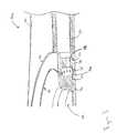
- FIG. 2Adepicts the bottom surface of an illustrative embodiment of a Bernoulli end effector 20 b that may be used in the system 10 .
- FIG. 2Bshows a cross-sectional view of the Bernoulli end effector 20 ′ of FIG. 2B .
- the Bernoulli end effector 20 bincludes a support member 22 , a series of passages 24 , an arm 26 , at least one edge guide 28 , and at least one friction pad 30 .
- Bernoulli end effectorsare particularly useful for ultra-thin wafers because they not only lift the wafers, but they also hold the wafers flat.
- the Bernoulli end effectorsare also advantageous because they can lift a wafer that has bowed or flexed while preventing the wafer from contacting the end effector. Larger diameter wafers and thinner wafers have a greater tendency to bow. For example, an ultra-thin wafer resting on a flat surface may bow or flex as much as 1 cm.
- By adjusting the distance between the wafer and the end effector prior to lifting or by adjusting the fluid flow rateone can compensate for the bow or flex of the ultra-thin wafers.
- Features of the inventionsuch as the edge guides and friction pads, can be included on the Bernoulli end effector to improve positioning and centering of the wafers on the end effector and impede motion of the substrate while the end effector is being translated or rotated.
- the support member 22is fixedly attached to the arm 26 .
- the arm 26may be the robotic arm 12 shown in FIG. 1 , or may be connectable to the robotic arm 12 .
- the support member 22 and the arm 26are metal, although they need not be the same material. Suitable metals include, but are not limited to, aluminum, stainless steel, and titanium.
- the support member 22 and the arm 26may also be a composite material or a metal alloy. According to the embodiment depicted in FIG. 2B , the support member 22 protrudes below the bottom surface of the arm 26 . In an alternative embodiment, the support member 22 and the arm 26 are flush on the bottom surface. In yet another embodiment, the arm 26 protrudes below the support member 22 .
- the support member 22has a series of passages 24 bored into it.
- the passages 24direct a fluid at a substrate, e.g., an ultra-thin wafer (not shown), to apply a holding force and/or a drag force to the surface of the wafer.
- the drag forceis a lateral force applied to the substrate 14 to push the wafer against the edge guides 28 .
- the passages 24may be bored by a drill, by Electrical Discharge Machining (EDM), or by laser drilling.
- EDMElectrical Discharge Machining
- the fluidcan be a liquid or a gas. Suitable gases include, but are not limited to, dry nitrogen, air, argon, or helium. Typical flow rates can range from about five standard liters per minute (SLM) to about 20 SLM (the greater the flow rate, the greater the holding force applied to the wafer).
- the cross-section of the passages 24is circular.
- the cross-sectionalso may be square, rectangular, elliptical, or oblong.
- the distance between the support member and the ultra-thin wafer prior to applying the holding forceis typically about 2 mm to about 12 mm. In one embodiment, the distance is about 2 mm to about 3 mm, which prevents the wafer from being lifted too abruptly and crashing into the bottom surface of the support member 22 or the arm 26 .
- the passages 24are bored into the support member 22 at an angle relative to the surface of the support member.
- a typical angleis about 30°, although the angle may be between about 10° and about 40°.
- a shallow angleis preferred so that the fluid contacts the substrate at a glancing angle. This allows for the ultra-thin wafer to be in closer proximity to the bottom surface of the support member 22 and provides a greater holding force to the wafer. Shallow angles increase the amount of material that must be drilled to form the passage 24 , and thus increases the cost of machining.
- the passages 24can be between about 0.010 inch and 0.020 inch in diameter, and preferably between about 0.010 in and about 0.012 inch, although smaller diameter passages can be drilled. Like the angle of the passages, the smaller bores require a greater cost. In one embodiment, the angle would be as shallow as, the diameter would be as small as, and the spacing would be as close as the material and fabrication methods permit. This provides for the most efficient hold force, and minimize the probability of damaging the ultra-thin wafer.
- the passages 24can be arranged symmetrically around the central axis of the support member 22 or can be arranged asymmetrically.
- a first series of passagesis arranged around the central axis in a circular pattern 32 .
- This pattern 32delivers the hold force to the substrate, while a second series of passages arranged in an arc pattern 34 delivers the drag force.
- the fluid source for the circular pattern 32 and the arc pattern 34may be separate, or may be the same.
- forty passagesare distributed around the circular pattern 32 with about a 9° spacing
- thirteen holesare distributed around the arc pattern 34 with about a 10° spacing.
- a single series of passages 24is arranged around the central axis in a circular pattern.
- the distribution of passages 24is varied around the single circle such that the density of passages is greater in the region applying the drag force.
- the passages 24are fed by the same fluid source.
- the edge guides 28contact an edge of the ultra-thin wafer and oppose the drag force applied by the fluid.
- the edge guides 28are in mechanical communication with either the support member 22 or the arm 26 .
- the edge guides 28are distributed between the support member 22 and the arm 26 .
- the edge guides 28protrude below the bottom surface of the support member 22 .
- the edge guides 28protrude about 1 mm below the surface of the support member 22 .
- the edge guides 28protrude about 2 mm below the surface of the support member 22 .
- the edge guides 28are ultra-high molecular weight polyethylene (UHMWPE).
- the edge guides 28may contact the wafer with a flat edge or a curved edge.
- the width or diameter of the edge guides 28may be between about 1 mm and about 6 mm.
- the edge guidesare cylindrical with a diameter of between about 3 mm and about 5 mm.
- the edge guides 28are beveled. If the wafer is slightly off-center, the beveled edge gently urges the wafer back on center. In one embodiment, there are between about two and about twenty edge guides, although more edge guides may be used. In one embodiment, fourteen edge guides are used.
- the support member 22includes friction pads 30 for contacting a surface of an ultra-thin wafer and/or impeding motion of the wafer.
- the friction pads 30inhibit the wafer from sliding out of position.
- the friction pads 30can reduce or preclude rotational motion of the wafer.
- the friction pads 30can be attached to a edge guide 28 .
- the friction pads 30may be positioned between adjacent edge guides 28 .
- the friction pads 30contact the substrate within a 2 mm wide edge exclusion zone. Contact in this zone is permitted during processing because wafer devices are not typically placed in this region, and thus the wafer is not contaminated.
- the friction pads 30may be formed from alumina or an elastomer, such as VITON® fluoroelastomer and KALREZ® perfluoroelastomer (available from DuPont Dow Elastomer, LLC).
- the friction pads 30may be circular, square, rectangular, or oblong. In various embodiments, the friction pads are between about 1 mm 2 and about 2 mm 2 . In one embodiment, the friction pads are about 1 ⁇ 1.75 mm. In another embodiment, the friction pads are about 1 ⁇ 1 mm.
- the Bernoulli end effector 20 bincludes a sensor, e.g., a camera or other sensor known in the art.
- the sensormonitors the performance characteristics of the end effector, including, but not limited to, fluid pressure and fluid flow rate.
- the sensormay also monitor the substrate characteristics, such as position, orientation, or simply just the presence of a substrate.
- the sensormay be in mechanical communication with or close proximity to the Bernoulli end effector 20 b.
- the hold force and the drag forceare applied simultaneously to the ultra-thin wafer to lift the wafer and urge an edge of the wafer into contact with the edge guides 28 .
- the hold force and the drag forcecan be applied separately.
- the hold force and the drag forcecan be applied first, and then the drag force is applied after a short delay. Typical delays are between about 100 ms to about 250 ms.
- FIG. 3depicts a section of an exemplary Bernoulli end effector 20 c formed from component pieces.
- the end effector 20 cincludes a cap ring 36 , a nozzle ring 38 , and an arm 40 .
- the component piecesmay be epoxied at points of intersection 42 to prevent fluid from escaping the end effector 20 c .
- the cap ring 36may include a cavity 44 to decrease its weight.
- the nozzle ring 38includes a plurality of passages 24 ′ that deliver fluid to the surface of a substrate (not shown).
- a cavity 46is defined by the cap ring 36 and the nozzle ring 38 , and the plurality of passages 24 ′ are connected to the cavity 46 , which assists in the delivery of the fluid to the passages 24 ′.
- the nozzle ring 38also includes a fluid passage 48 to connect the cavity 46 to a fluid channel 50 in the arm 40 .
- the fluid passage 48can be, for example, about 0.047 inch diameter.
- the fluid channel 50directs fluid from a fluid source (not shown) to the passages 24 ′.
- the fluid channel 50is formed by milling a trough in the arm 40 , and then affixing a thin piece of metal, e.g., a 0.01 inch stainless steel ribbon, along the length of the fluid channel 50 to seal it.
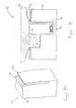
- FIG. 4depicts an illustrative embodiment of an apparatus 52 for supinating a substrate 14 having a first surface 54 and a second surface 56 .
- the apparatus 52includes an end effector 20 d , and a first substrate chuck 58 and a second substrate chuck 60 attached to a mount 62 .
- an ultra-thin wafermay be supinated so that both sides of the wafer can be processed. For example, flipping the wafer permits further processing of the underside, such as metallization.
- the end effector 20 dhas the ability to translate in the horizontal plane or rotate about its longitudinal axis.
- the end effector 20 dmay deliver the substrate 14 to the first chuck 58 , and then rotate 180° about its longitudinal axis to receive the substrate from the second substrate chuck 60 .
- the mount 62may have the ability to rotate about an axis parallel to the plane of the substrate chucks 58 and 60 .
- the end effector 20 dthen receives the substrate 14 from the second susbtrate chuck 60 after the substrate 14 is transferred between chucks.
- the end effector 20 ddelivers to the first substrate chuck 58 the substrate 14 with the first surface 54 exposed.
- the second substrate chuck 60is spaced in opposition to the first substrate chuck 58 , and provides sufficient space for the end effector 20 d to place the substrate 14 without contacting either chuck 58 or 60 .
- Either the first chuck 58 or the second chuck 60may be mounted on an actuator, so that the distance between the chucks 58 and 60 can be controlled prior to transferring the substrate 14 .
- the distance between the chucks 58 and 60may be between about 1 mm and about 12 mm during transfer, although a smaller distance (about 1 mm to about 2 mm) is preferred so that an ultra-thin wafer is not damaged.
- Transfer of the substrate 14is accomplished by substantially simultaneously turning off the first substrate chuck 58 and turning on the second substrate chuck 60 .
- the second substrate chuck 60receives the substrate 14 from the first substrate chuck 58 , thereby exposing the second surface 56 of the substrate 14 .
- the end effector 20 dis then positioned to receive the substrate 14 from the second substrate chuck 60 after the substrate 14 is flipped.
- the apparatus 52includes a sensor and/or electronics to determine the position or orientation of the substrate 14 prior to, during, and/or after supination. If the sensor determines that the substrate 14 is not positioned correctly, it may rotate either the first chuck 58 or the second chuck 60 , so that the position will be corrected.
- the sensormay be a camera or other sensor known in the art. The sensor may be attached to either the first chuck 58 or the second chuck 60 .
- the end effector 20 dmay be attached to a robotic arm that supinates the end effector 20 d prior to receiving the substrate 14 from the second substrate chuck 60 . After receiving the substrate 14 , the end effector 20 d may be inverted a second time so that the second surface 56 of the substrate 14 faces downward.
- the mount 62is rotatable, so that the substrate 14 may be supinated while being lifted by one of the two substrate chucks 58 and 60 .
- Either of the two substrate chucks 58 and 60may be either a Bernoulli chuck or an electrostatic chuck.
- the end effector 20 dmay be a Bernoulli end effector, such as the Bernoulli end effectors 20 b or 20 c described above.
- Bernoulli end effectors and chucksare particularly advantageous for ultra-thin semiconductor wafers because they provide a contact free lifting device and because they hold the wafers flat.
- FIG. 5depicts an illustrative embodiment of a Bernoulli chuck 58 ′ for use with the apparatus 52 depicted in FIG. 4 .
- the chuck 58 ′includes a support member 22 ′, a series of passages 24 ′′ for delivering a fluid to a substrate, friction pads 30 ′, and cut-outs 64 in the support member 22 ′.
- the passagesare located closer to the perimeter of the support member 22 ′ than, for example, in the Bernoulli end effectors described above.
- the friction pads 30 ′are positioned around the entire perimeter of the support member 22 ′ to provide additional resistance to rotational or translational motion of the wafer when it is supinated.
- the cut-outs 64reduce the weight of the support member 22 ′.
- FIG. 6shows a cross-sectional view of an exemplary substrate handling structure 18 ′ according to the invention.
- the structure 18 ′includes a substrate carrier 66 , a substrate support feature 68 , a substrate clamp, at least one guide 70 , and a secondary base 74 .
- the substrate 14is placed on the substrate support feature 68 of the substrate carrier 66 .
- the substrate clamp 70holds the substrate 14 flat during processing of the substrate 14 . After processing, the substrate 14 , and particularly ultra-thin wafers, are more susceptible to curling, bowing or flexing due to stress applied, e.g., by a film deposited.
- the substrate clamp 70also maintains the shape of the substrate 14 until an end effector can remove the substrate from the substrate carrier 66 .
- the substrate clamp 70is moveable between a lowered position for securing the substrate 14 and a raised position, which permits the substrate 14 to be placed or retrieved, e.g., by one of the end effectors 20 a , 20 b , 20 c , or 20 d.
- the substratesare so thin, they may be analogized to a piece of paper resting on a table. The slightest displacement of air may cause the substrate to move.
- the guides 72impede lateral movement of the substrate 14 when the substrate clamp 70 is in the raised position. When the substrate clamp 70 is lowered, the guides 72 may retract below the surface of the substrate carrier 66 .
- the guides 72may be attached to the substrate carrier 66 or to the secondary base 74 .
- the guides 72also may serve as pins that raise or lower the substrate clamp when the guides 72 are actuated.
- the guides 72may be spring loaded, so that they pop-up when the substrate clamp 70 is raised.
- the guidemay be located in a recess or cavity in the substrate carrier.
- the substrate clamp 70is constructed to only cover the edge of the substrate 14 .
- the substrate clamp 70may have a beveled edge.
- the substrate clamp 70may contact the edge of the wafer as the substrate clamp 70 is lowered. If the ultra-thin wafer is not centered on the substrate support feature 68 , the beveled edge will gently nudge the wafer toward the center of the support feature 68 as the substrate clamp 70 is lowered.
- the substrate clamp 70may be constructed in sections. For example, if multiple sections are used, then one section may be raised to expose between about 25% and about 40% of the edge of an ultra-thin wafer. The wafer remains flat until the Bernoulli end effector can be introduced to lift the wafer from the carrier.
- FIG. 7Ashows an exemplary guide 72 ′ for impeding lateral movement of a substrate (not shown).
- the guide 72 ′includes a rigid portion 76 , a flexible portion 78 , and a ridge 80 .
- the rigid portion 76forms the body of the guide 72 ′.
- the flexible portion 78contacts the edge of the substrate. It provides a pliant surface that minimizes the stress applied to the edge of an ultra-thin wafer.
- the ridge 80is disposed to contact the substrate clamp (not shown), thereby preventing the substrate clamp from contacting the more fragile flexible portion 78 .
- the rigid portion 76 and the flexible portion 78are metal, although they need not be the same material. Suitable metals include, but are not limited to, aluminum, stainless steel, and titanium.
- the portions 76 and 78also may be a composite material or a metal alloy.
- FIG. 7Bdepicts a cross-sectional view of the guide 72 ′ placed in a recess 82 formed in the substrate carrier 66 ′ of an exemplary substrate handling structure 18 ′′.
- the structure 18 ′′includes a substrate clamp 70 ′ for holding the substrate 14 flat before, during, and after processing.
- the substrate clamp 70 ′when lowered, forces the guide 72 ′ into the recess 82 .
- a spring 84forces the guide 72 ′ up, and the flexible portion of the guide 72 ′ contacts the substrate 14 .
Landscapes
- Engineering & Computer Science (AREA)
- Physics & Mathematics (AREA)
- Condensed Matter Physics & Semiconductors (AREA)
- General Physics & Mathematics (AREA)
- Manufacturing & Machinery (AREA)
- Computer Hardware Design (AREA)
- Microelectronics & Electronic Packaging (AREA)
- Power Engineering (AREA)
- Container, Conveyance, Adherence, Positioning, Of Wafer (AREA)
- Manipulator (AREA)
Abstract
Description
- The invention relates generally to the field of substrates for integrated circuits, and more particularly to methods and systems for holding, handling, and transporting ultra-thin wafers.
- As portable electronic devices, micro-electromechanical systems (MEMS), and smart cards become smaller and thinner, so too must the integrated circuits from which they are fabricated. Thin circuits not only consume less space, they also allow for more functionality per unit volume, increase power dissipation, and provide for a mechanically flexible device that may conform to curved surfaces. Thin circuits are typically fabricated on ultra-thin substrates, such as ultra-thin silicon wafers. Typical dimensions of ultra-thin wafers are about 60 μm to 80 μm, while the theoretical limit for suitable thin wafers is about 10 μm.
- Bernoulli end effectors have been used in various applications to handle thin substrates. Bernoulli end effectors use a support member with fluid exhaust ports brought into close proximity with the top side of a substrate. The exhaust ports are configured so that the gas flow creates a low pressure region on the top side of the substrate causing it to lift up toward the support member. The substrate can be lifted from a substantially flat surface and transported from the top side of the substrate without contacting the top side. Contacting a semiconductor wafer during processing typically contaminates it, thus decreasing the yield from individual semiconductor wafers.
- A disadvantage of many prior art Bernoulli end effectors is that they do not provide guides to position the substrate, and thus do not provide for high precision centering of the substrate. Another disadvantage is that the holding mechanism restricts the transport motion to paths within a horizontal plane or perpendicular to a horizontal plane.
- Disadvantages of thin substrates include processing difficulties, such as cracking, bowing, or flexing during lifting, holding, handling, and transporting the substrates. Bernoulli end effectors can transfer thin substrates, but many substrate cassettes and assembly area tools cannot accommodate them. Further, a method for processing both sides of a substrate is desirable, but supinating or flipping a substrate is difficult.
- The present invention features, at least in part an improved Bernoulli end effector for holding, handling, and transporting thin substrates. The end effector includes edge guides to aid in the positioning of the substrate and also includes friction pads that impede rotational and translational motion of the substrate lifted by the end effector. The friction pads may contact, for example, the outer 2 mm of the edge of the substrate. The friction pads permit the Bernoulli end effector to be translated and/or elevated at a greater rate of speed, while reducing the likelihood that holding, centering or anti-rotation forces will be compromised.
- The present invention also provides an apparatus and method for supinating a substrate so that both surfaces of the substrate may be processed. The apparatus may include a Bernoulli end effector to deliver a substrate to a system of chucks, which may be rotatably mounted. The apparatus also may include a sensor to monitor the position of the substrate prior to being transferred.
- The present invention also provides a substrate handling structure that prevents a thin substrate from bowing or flexing during processing, and also provides guides that prevent the thin substrate from moving or translating on the surface of the substrate handling structure. The guides prevent the substrate from moving, which improves the accuracy of the positioning of the substrate. This is particularly important if/when the substrate bows or flexes due to its thinness and/or stresses placed on the substrate.
- Accordingly, in a first aspect, the invention provides a Bernoulli end effector including a support member defining at least one passage for directing a fluid at a substrate to apply a holding force and a drag force on the substrate; at least one edge guide in mechanical communication with the support member for contacting an edge of the substrate to oppose the drag force applied by the fluid; and at least one friction pad in mechanical communication with the support member for contacting a surface of the substrate to impede a rotational motion of the substrate. At least one friction pad may be attached to at least one edge guide. The end effector may include a first plurality of passages symmetrically arranged about an axis of the support member and a second plurality of passages asymmetrically arranged about the axis of the support member. The first plurality of passages may be arranged in a circular pattern for providing a Bernoulli force perpendicular to a surface of the substrate. The second plurality of passages may be arranged in an arc for providing the drag force on the substrate.
- The Bernoulli end effector can include an angle between a direction defined by the passages and a surface of the support member. The angle may be between about twenty and thirty degrees. The friction pads can be disposed for contacting the substrate within 2 mm of an edge of the substrate. The friction pad may be an elastomer or alumina. The edge guides can be beveled. The holding force can be applied first and then the drag force may be applied after a delay (e.g., between about 100 ms and 250 ms).
- In another aspect, the invention features a method for handling a substrate with a Bernoulli end effector. The method includes directing a fluid at the substrate to apply a holding force and a drag force to the substrate; applying a counter force to an edge of the substrate to oppose the drag force; and applying a frictional force to a surface of the substrate adjacent to the edge of the substrate to impede a rotational motion of the substrate. The holding force creates a low pressure Bernoulli force to lift the substrate. In one embodiment, the holding force is first applied and then the drag force is applied after a delay.
- In still another aspect, the invention provides a method for handling a substrate with a Bernoulli end effector. The method includes directing a fluid at the substrate to apply a holding force to the substrate; applying a drag force after applying the holding force; and applying a counter force to an edge of the substrate to oppose the drag force. The method can include applying a frictional force to a surface of the substrate adjacent to the edge of the substrate to impede a rotational motion of the substrate.
- In yet another aspect, the invention provides a substrate handling structure including a substrate carrier having a substrate support feature; a substrate clamp moveable between a lowered position for securing a substrate on the substrate support feature and a raised position to permit placing the substrate on the substrate support feature; and at least one guide disposed adjacent to the substrate support feature for impeding a lateral movement of the substrate when the substrate clamp is in the raised position. The at least one guide can be retractably mounted for retracting the at least one guide when the substrate clamp secures the substrate. The substrate clamp can be configured to cause the at least one guide to retract when the substrate clamp is moved from the raised position to the lowered position.
- In one embodiment of the substrate handling structure, the substrate clamp is configured to cover only a surface portion adjacent to an edge of the substrate. The substrate clamp can include a beveled edge portion configured to contact the substrate and center the substrate on the substrate support feature. The guide can include a spring that urges the guide to project above a surface of the substrate carrier. The guide may be attached to the substrate carrier. The substrate carrier can define at least one cavity within which the at least one guide is moveably mounted. The guide can include a first portion and a second portion that is flexibly attached to the first portion, the second portion for contacting the substrate.
- In still another aspect, the invention provides an apparatus for supinating a substrate. The apparatus includes a first substrate chuck for securing the substrate while a first surface of the substrate is exposed; a second substrate chuck spaced in opposition to the first substrate chuck for securing the substrate after receiving the substrate from the first substrate chuck to expose a second surface of the substrate; and an end effector for either delivering the substrate to the first substrate chuck or receiving the substrate from the second substrate chuck. In one embodiment, the end effector is rotatably mounted for rotating the substrate about an axis parallel to a face of the substrate or for rotating after delivering a substrate to the first or second substrate chuck. In another embodiment, the first chuck and the second chuck are each fixedly mounted. In various embodiments, the first chuck and the second chuck are mounted in a fixed relationship to each other, and together are rotatably mounted for rotating a substrate secured by one of the first and second chucks. At least one of the first and second chucks may be either a Bernoulli chuck or an electrostatic chuck. In various embodiments of the apparatus, the end effector is a Bernoulli end effector. The apparatus can include an actuator in mechanical communication with the first substrate chuck. The actuator controls the spacing between the first substrate chuck and the second substrate chuck. The apparatus also can include a sensor (e.g., a camera) for monitoring the position of the substrate. The sensor may be integrated with at least one of the chucks.
- In another aspect, the invention provides a method for supinating a substrate. The method includes securing a substrate with a first substrate chuck such that a first surface of the substrate faces the first substrate chuck; transferring the substrate to a second substrate chuck that is spaced in opposition to the first substrate chuck such that a second surface of the substrate faces the second substrate chuck; and receiving the substrate from the second substrate chuck to expose the second surface of the substrate. The method can include transferring, by an end effector, the substrate to the first substrate chuck. The method also may include rotating a portion of the end effector after transferring the substrate to the first substrate chuck and before receiving the substrate by the end effector. In one embodiment, the method includes translating at least one of the first substrate chuck and the second substrate chuck to control the spacing between the chucks prior to transferring the substrate.
- Other aspects and advantages of the invention will become apparent from the following drawings, detailed description, and claims, all of which illustrate the principles of the invention, by way of example only.
- The advantages of the invention described above, together with further advantages, may be better understood by referring to the following description taken in conjunction with the accompanying drawings. In the drawings, like reference characters generally refer to the same parts throughout the different views. The drawings are not necessarily to scale, emphasis instead generally being placed upon illustrating the principles of the invention.
FIG. 1 is a top view of an embodiment of a substrate handling system;FIG. 2A is a bottom view of an embodiment of a Bernoulli end effector according to the invention;FIG. 2B is a cross-sectional view of the Bernoulli end effector shown inFIG. 2B ;FIG. 3 is a sectional elevation of an exemplary Bernoulli end effector according to the invention;FIG. 4 is a perspective view of an embodiment of a system for supinating a substrate, according to the invention;FIG. 5 is a top view of an embodiment of a Bernoulli chuck for use with the system depicted inFIG. 4 ;FIG. 6 is a cross-sectional view of an exemplary substrate handling structure according to the invention;FIG. 7A is a perspective view of an embodiment of a guide for a substrate, according to the invention; andFIG. 7B is a cross-sectional view of the guide ofFIG. 7A disposed in an exemplary substrate handling structure.FIG. 1 is a top view of an embodiment of asubstrate handling system 10 that may benefit from features of the invention. Such asystem 10 may be a component piece or tool of an in-line processing apparatus, e.g., described in U.S. Pat. No. 6,217,272 to Felsenthal et al. and U.S. Pat. No. 6,530,733 to Klein et al., the entire disclosures of which are hereby incorporated by reference. Thesystem 10 includes arobot arm 12 that transports asubstrate 14 or a batch ofsubstrates 14 from a substrate carrier16 and places them on a substrate handling structure18 (e.g., a wafer tray or any type of substrate carrier known in the art). Thesubstrates 14 may be, e.g., semiconductor wafers or glass substrates. The diameter of thesubstrates 14 may be, e.g., about 125 mm, about 150 mm, about 200 mm, about 250 mm, or about 300 mm. The thickness of thesubstrates 14 may be between about 10 μm and about 750 μm. Typical dimensions of an ultra-thin wafer are a diameter of about 150 mm and a thickness of about 80 μm, although, as will be described below, the features of the invention become more helpful as the diameter of the wafer becomes larger, and the thickness of the wafer becomes smaller.- The
robot arm 12 may be any type known in the art, and is typically computer controlled. In one embodiment, therobot arm 12 is a rotatable multi-segmented arm that is positionable between a first position proximate to the substrate carrier16 (as shown in dotted view) and a second position that is proximate to thesubstrate handling structure 18. Therobot arm 12 is movable vertically to enable it to load and unload substrates from different vertical levels of the substrate carrier16. Thesubstrate handling structure 18 may be located in a load lock chamber, which transfers thesubstrates 14 from atmosphere to vacuum for processing. - Typically, the
robot arm 12 includes anend effector 20afor lifting thesubstrates 14 from the substrate carrier16 and transferring them to thesubstrate handling structure 18. In one embodiment, the end effector is a Bernoulli end effector. In another embodiment, the end effector is an electrostatic chuck, although vacuum end effectors and edge clamp end effectors may be used. FIG. 2A depicts the bottom surface of an illustrative embodiment of a Bernoulli end effector20bthat may be used in thesystem 10.FIG. 2B shows a cross-sectional view of the Bernoulli end effector20′ ofFIG. 2B . The Bernoulli end effector20bincludes asupport member 22, a series ofpassages 24, anarm 26, at least oneedge guide 28, and at least onefriction pad 30.- Bernoulli end effectors are particularly useful for ultra-thin wafers because they not only lift the wafers, but they also hold the wafers flat. The Bernoulli end effectors are also advantageous because they can lift a wafer that has bowed or flexed while preventing the wafer from contacting the end effector. Larger diameter wafers and thinner wafers have a greater tendency to bow. For example, an ultra-thin wafer resting on a flat surface may bow or flex as much as 1 cm. By adjusting the distance between the wafer and the end effector prior to lifting or by adjusting the fluid flow rate, one can compensate for the bow or flex of the ultra-thin wafers. Features of the invention, such as the edge guides and friction pads, can be included on the Bernoulli end effector to improve positioning and centering of the wafers on the end effector and impede motion of the substrate while the end effector is being translated or rotated.
- According to the illustrative embodiment, the
support member 22 is fixedly attached to thearm 26. Thearm 26 may be therobotic arm 12 shown inFIG. 1 , or may be connectable to therobotic arm 12. In one embodiment, thesupport member 22 and thearm 26 are metal, although they need not be the same material. Suitable metals include, but are not limited to, aluminum, stainless steel, and titanium. Thesupport member 22 and thearm 26 may also be a composite material or a metal alloy. According to the embodiment depicted inFIG. 2B , thesupport member 22 protrudes below the bottom surface of thearm 26. In an alternative embodiment, thesupport member 22 and thearm 26 are flush on the bottom surface. In yet another embodiment, thearm 26 protrudes below thesupport member 22. - According to the illustrative embodiment, the
support member 22 has a series ofpassages 24 bored into it. Thepassages 24 direct a fluid at a substrate, e.g., an ultra-thin wafer (not shown), to apply a holding force and/or a drag force to the surface of the wafer. The drag force is a lateral force applied to thesubstrate 14 to push the wafer against the edge guides28. Thepassages 24 may be bored by a drill, by Electrical Discharge Machining (EDM), or by laser drilling. The fluid can be a liquid or a gas. Suitable gases include, but are not limited to, dry nitrogen, air, argon, or helium. Typical flow rates can range from about five standard liters per minute (SLM) to about 20 SLM (the greater the flow rate, the greater the holding force applied to the wafer). - According to the illustrative embodiment, the cross-section of the
passages 24 is circular. The cross-section also may be square, rectangular, elliptical, or oblong. The distance between the support member and the ultra-thin wafer prior to applying the holding force is typically about 2 mm to about 12 mm. In one embodiment, the distance is about 2 mm to about 3 mm, which prevents the wafer from being lifted too abruptly and crashing into the bottom surface of thesupport member 22 or thearm 26. - In one embodiment, the
passages 24 are bored into thesupport member 22 at an angle relative to the surface of the support member. A typical angle is about 30°, although the angle may be between about 10° and about 40°. A shallow angle is preferred so that the fluid contacts the substrate at a glancing angle. This allows for the ultra-thin wafer to be in closer proximity to the bottom surface of thesupport member 22 and provides a greater holding force to the wafer. Shallow angles increase the amount of material that must be drilled to form thepassage 24, and thus increases the cost of machining. - In one embodiment, the
passages 24 can be between about 0.010 inch and 0.020 inch in diameter, and preferably between about 0.010 in and about 0.012 inch, although smaller diameter passages can be drilled. Like the angle of the passages, the smaller bores require a greater cost. In one embodiment, the angle would be as shallow as, the diameter would be as small as, and the spacing would be as close as the material and fabrication methods permit. This provides for the most efficient hold force, and minimize the probability of damaging the ultra-thin wafer. - The
passages 24 can be arranged symmetrically around the central axis of thesupport member 22 or can be arranged asymmetrically. For example, as shown inFIG. 2A , a first series of passages is arranged around the central axis in acircular pattern 32. Thispattern 32 delivers the hold force to the substrate, while a second series of passages arranged in anarc pattern 34 delivers the drag force. The fluid source for thecircular pattern 32 and thearc pattern 34 may be separate, or may be the same. In an exemplary embodiment, forty passages are distributed around thecircular pattern 32 with about a 9° spacing, and thirteen holes are distributed around thearc pattern 34 with about a 10° spacing. - In an alternative embodiment, a single series of
passages 24 is arranged around the central axis in a circular pattern. The distribution ofpassages 24 is varied around the single circle such that the density of passages is greater in the region applying the drag force. In this embodiment, thepassages 24 are fed by the same fluid source. - The edge guides28 contact an edge of the ultra-thin wafer and oppose the drag force applied by the fluid. In various embodiments, the edge guides28 are in mechanical communication with either the
support member 22 or thearm 26. In an alternative embodiment, the edge guides28 are distributed between thesupport member 22 and thearm 26. According to the illustrative embodiment, the edge guides28 protrude below the bottom surface of thesupport member 22. In one embodiment, the edge guides28 protrude about 1 mm below the surface of thesupport member 22. In another embodiment, the edge guides28 protrude about 2 mm below the surface of thesupport member 22. In various embodiments, the edge guides28 are ultra-high molecular weight polyethylene (UHMWPE). The edge guides28 may contact the wafer with a flat edge or a curved edge. The width or diameter of the edge guides28 may be between about 1 mm and about 6 mm. Preferably, the edge guides are cylindrical with a diameter of between about 3 mm and about 5 mm. In one embodiment, the edge guides28 are beveled. If the wafer is slightly off-center, the beveled edge gently urges the wafer back on center. In one embodiment, there are between about two and about twenty edge guides, although more edge guides may be used. In one embodiment, fourteen edge guides are used. - According to the illustrative embodiment, the
support member 22 includesfriction pads 30 for contacting a surface of an ultra-thin wafer and/or impeding motion of the wafer. For example, when the end effector is translated horizontally, thefriction pads 30 inhibit the wafer from sliding out of position. Thefriction pads 30 can reduce or preclude rotational motion of the wafer. Thefriction pads 30 can be attached to aedge guide 28. Alternatively, thefriction pads 30 may be positioned between adjacent edge guides28. - In one embodiment, the
friction pads 30 contact the substrate within a 2 mm wide edge exclusion zone. Contact in this zone is permitted during processing because wafer devices are not typically placed in this region, and thus the wafer is not contaminated. Thefriction pads 30 may be formed from alumina or an elastomer, such as VITON® fluoroelastomer and KALREZ® perfluoroelastomer (available from DuPont Dow Elastomer, LLC). Thefriction pads 30 may be circular, square, rectangular, or oblong. In various embodiments, the friction pads are between about 1 mm2and about 2 mm2. In one embodiment, the friction pads are about 1×1.75 mm. In another embodiment, the friction pads are about 1×1 mm. - In various embodiments, the Bernoulli end effector20bincludes a sensor, e.g., a camera or other sensor known in the art. The sensor monitors the performance characteristics of the end effector, including, but not limited to, fluid pressure and fluid flow rate. The sensor may also monitor the substrate characteristics, such as position, orientation, or simply just the presence of a substrate. The sensor may be in mechanical communication with or close proximity to the Bernoulli end effector20b.
- In one embodiment of the Bernoulli end effector20b, the hold force and the drag force are applied simultaneously to the ultra-thin wafer to lift the wafer and urge an edge of the wafer into contact with the edge guides28. In an alternative embodiment, where the fluid source for the patterns of
passages FIG. 3 depicts a section of an exemplary Bernoulli end effector20cformed from component pieces. The end effector20cincludes acap ring 36, a nozzle ring38, and anarm 40. The component pieces may be epoxied at points ofintersection 42 to prevent fluid from escaping the end effector20c. Thecap ring 36 may include acavity 44 to decrease its weight. The nozzle ring38 includes a plurality ofpassages 24′ that deliver fluid to the surface of a substrate (not shown). Acavity 46 is defined by thecap ring 36 and the nozzle ring38, and the plurality ofpassages 24′ are connected to thecavity 46, which assists in the delivery of the fluid to thepassages 24′. The nozzle ring38 also includes afluid passage 48 to connect thecavity 46 to afluid channel 50 in thearm 40. Thefluid passage 48 can be, for example, about 0.047 inch diameter. Thefluid channel 50 directs fluid from a fluid source (not shown) to thepassages 24′. In one embodiment, thefluid channel 50 is formed by milling a trough in thearm 40, and then affixing a thin piece of metal, e.g., a 0.01 inch stainless steel ribbon, along the length of thefluid channel 50 to seal it.FIG. 4 depicts an illustrative embodiment of anapparatus 52 for supinating asubstrate 14 having afirst surface 54 and asecond surface 56. Theapparatus 52 includes anend effector 20d, and afirst substrate chuck 58 and asecond substrate chuck 60 attached to amount 62. During semiconductor wafer processing, an ultra-thin wafer may be supinated so that both sides of the wafer can be processed. For example, flipping the wafer permits further processing of the underside, such as metallization.- To supinate an ultra-thin wafer, the two opposing
chucks end effector 20dhas the ability to translate in the horizontal plane or rotate about its longitudinal axis. Theend effector 20dmay deliver thesubstrate 14 to thefirst chuck 58, and then rotate 180° about its longitudinal axis to receive the substrate from thesecond substrate chuck 60. Alternatively, themount 62 may have the ability to rotate about an axis parallel to the plane of the substrate chucks58 and60. Theend effector 20dthen receives thesubstrate 14 from thesecond susbtrate chuck 60 after thesubstrate 14 is transferred between chucks. - According to the illustrative embodiment, the
end effector 20ddelivers to thefirst substrate chuck 58 thesubstrate 14 with thefirst surface 54 exposed. Thesecond substrate chuck 60 is spaced in opposition to thefirst substrate chuck 58, and provides sufficient space for theend effector 20dto place thesubstrate 14 without contacting either chuck58 or60. Either thefirst chuck 58 or thesecond chuck 60 may be mounted on an actuator, so that the distance between thechucks substrate 14. The distance between thechucks - Transfer of the
substrate 14 is accomplished by substantially simultaneously turning off thefirst substrate chuck 58 and turning on thesecond substrate chuck 60. Thesecond substrate chuck 60 receives thesubstrate 14 from thefirst substrate chuck 58, thereby exposing thesecond surface 56 of thesubstrate 14. Theend effector 20dis then positioned to receive thesubstrate 14 from thesecond substrate chuck 60 after thesubstrate 14 is flipped. - In one embodiment, the
apparatus 52 includes a sensor and/or electronics to determine the position or orientation of thesubstrate 14 prior to, during, and/or after supination. If the sensor determines that thesubstrate 14 is not positioned correctly, it may rotate either thefirst chuck 58 or thesecond chuck 60, so that the position will be corrected. The sensor may be a camera or other sensor known in the art. The sensor may be attached to either thefirst chuck 58 or thesecond chuck 60. - In one embodiment, the
end effector 20dmay be attached to a robotic arm that supinates theend effector 20dprior to receiving thesubstrate 14 from thesecond substrate chuck 60. After receiving thesubstrate 14, theend effector 20dmay be inverted a second time so that thesecond surface 56 of thesubstrate 14 faces downward. In an alternative embodiment, themount 62 is rotatable, so that thesubstrate 14 may be supinated while being lifted by one of the two substrate chucks58 and60. - Either of the two substrate chucks58 and60 may be either a Bernoulli chuck or an electrostatic chuck. The
end effector 20dmay be a Bernoulli end effector, such as the Bernoulli end effectors20bor20cdescribed above. As described above, Bernoulli end effectors and chucks are particularly advantageous for ultra-thin semiconductor wafers because they provide a contact free lifting device and because they hold the wafers flat. FIG. 5 depicts an illustrative embodiment of aBernoulli chuck 58′ for use with theapparatus 52 depicted inFIG. 4 . Thechuck 58′ includes asupport member 22′, a series ofpassages 24″ for delivering a fluid to a substrate,friction pads 30′, and cut-outs 64 in thesupport member 22′. In this embodiment, the passages are located closer to the perimeter of thesupport member 22′ than, for example, in the Bernoulli end effectors described above. Having the passages closer to the edge of theBernoulli chuck 58′ provides a holding force closer to the edge of the wafer, which reduces the possibility of distortion of an ultra-thin wafer and, in particular, larger diameter wafers. In the illustrative embodiment, thefriction pads 30′ are positioned around the entire perimeter of thesupport member 22′ to provide additional resistance to rotational or translational motion of the wafer when it is supinated. The cut-outs 64 reduce the weight of thesupport member 22′.FIG. 6 shows a cross-sectional view of an exemplarysubstrate handling structure 18′ according to the invention. Thestructure 18′ includes a substrate carrier66, asubstrate support feature 68, a substrate clamp, at least oneguide 70, and asecondary base 74. Thesubstrate 14 is placed on thesubstrate support feature 68 of the substrate carrier66. Thesubstrate clamp 70 holds thesubstrate 14 flat during processing of thesubstrate 14. After processing, thesubstrate 14, and particularly ultra-thin wafers, are more susceptible to curling, bowing or flexing due to stress applied, e.g., by a film deposited. Thesubstrate clamp 70 also maintains the shape of thesubstrate 14 until an end effector can remove the substrate from the substrate carrier66. Thesubstrate clamp 70 is moveable between a lowered position for securing thesubstrate 14 and a raised position, which permits thesubstrate 14 to be placed or retrieved, e.g., by one of theend effectors - Because the substrates are so thin, they may be analogized to a piece of paper resting on a table. The slightest displacement of air may cause the substrate to move. The
guides 72 impede lateral movement of thesubstrate 14 when thesubstrate clamp 70 is in the raised position. When thesubstrate clamp 70 is lowered, theguides 72 may retract below the surface of the substrate carrier66. Theguides 72 may be attached to the substrate carrier66 or to thesecondary base 74. Theguides 72 also may serve as pins that raise or lower the substrate clamp when theguides 72 are actuated. In an alternative embodiment, theguides 72 may be spring loaded, so that they pop-up when thesubstrate clamp 70 is raised. In this embodiment, the guide may be located in a recess or cavity in the substrate carrier. - In one embodiment, the
substrate clamp 70 is constructed to only cover the edge of thesubstrate 14. Thesubstrate clamp 70 may have a beveled edge. Thesubstrate clamp 70 may contact the edge of the wafer as thesubstrate clamp 70 is lowered. If the ultra-thin wafer is not centered on thesubstrate support feature 68, the beveled edge will gently nudge the wafer toward the center of thesupport feature 68 as thesubstrate clamp 70 is lowered. - In addition, the
substrate clamp 70 may be constructed in sections. For example, if multiple sections are used, then one section may be raised to expose between about 25% and about 40% of the edge of an ultra-thin wafer. The wafer remains flat until the Bernoulli end effector can be introduced to lift the wafer from the carrier. FIG. 7A shows anexemplary guide 72′ for impeding lateral movement of a substrate (not shown). Theguide 72′ includes arigid portion 76, aflexible portion 78, and a ridge80. Therigid portion 76 forms the body of theguide 72′. Theflexible portion 78 contacts the edge of the substrate. It provides a pliant surface that minimizes the stress applied to the edge of an ultra-thin wafer. The ridge80 is disposed to contact the substrate clamp (not shown), thereby preventing the substrate clamp from contacting the more fragileflexible portion 78. In one embodiment, therigid portion 76 and theflexible portion 78 are metal, although they need not be the same material. Suitable metals include, but are not limited to, aluminum, stainless steel, and titanium. Theportions FIG. 7B depicts a cross-sectional view of theguide 72′ placed in arecess 82 formed in the substrate carrier66′ of an exemplarysubstrate handling structure 18″. As described above, thestructure 18″ includes asubstrate clamp 70′ for holding thesubstrate 14 flat before, during, and after processing. Thesubstrate clamp 70′, when lowered, forces theguide 72′ into therecess 82. When thesubstrate clamp 70′ is raised, aspring 84 forces theguide 72′ up, and the flexible portion of theguide 72′ contacts thesubstrate 14.- While the invention has been particularly shown and described with reference to specific illustrative embodiments, it should be understood that various changes in form and detail may be made without departing from the spirit and scope of the invention as defined by the appended claims.
Claims (58)
Priority Applications (1)
| Application Number | Priority Date | Filing Date | Title |
|---|---|---|---|
| US10/618,091US7100954B2 (en) | 2003-07-11 | 2003-07-11 | Ultra-thin wafer handling system |
Applications Claiming Priority (1)
| Application Number | Priority Date | Filing Date | Title |
|---|---|---|---|
| US10/618,091US7100954B2 (en) | 2003-07-11 | 2003-07-11 | Ultra-thin wafer handling system |
Publications (2)
| Publication Number | Publication Date |
|---|---|
| US20050110291A1true US20050110291A1 (en) | 2005-05-26 |
| US7100954B2 US7100954B2 (en) | 2006-09-05 |
Family
ID=34590545
Family Applications (1)
| Application Number | Title | Priority Date | Filing Date |
|---|---|---|---|
| US10/618,091Expired - LifetimeUS7100954B2 (en) | 2003-07-11 | 2003-07-11 | Ultra-thin wafer handling system |
Country Status (1)
| Country | Link |
|---|---|
| US (1) | US7100954B2 (en) |
Cited By (13)
| Publication number | Priority date | Publication date | Assignee | Title |
|---|---|---|---|---|
| WO2006072422A1 (en)* | 2005-01-04 | 2006-07-13 | Nanophotonics Ag | Gripper for holding and positioning a disc- or plate-shaped object and method for holding and positioning a disc- or plate-shaped object |
| US20090032060A1 (en)* | 2007-07-31 | 2009-02-05 | Kent Riley Child | Bernoulli blade |
| WO2013090898A1 (en)* | 2011-12-16 | 2013-06-20 | Brooks Automation, Inc. | Transport apparatus |
| JP2013219069A (en)* | 2012-04-04 | 2013-10-24 | Tokyo Electron Ltd | Device and method for holding substrate |
| US20140340509A1 (en)* | 2013-05-16 | 2014-11-20 | Kevin P Fairbairn | System and Method for Real Time Positioning of a Substrate in a Vacuum Processing System |
| TWI512877B (en)* | 2010-03-23 | 2015-12-11 | Nitto Denko Corp | Workpiece transport method and workpiece transport device |
| JP2016131188A (en)* | 2015-01-13 | 2016-07-21 | 株式会社ディスコ | Transport device |
| CN107342245A (en)* | 2016-04-06 | 2017-11-10 | 朗姆研究公司 | For EBR chuck and for making chip method placed in the middle before EBR |
| CN108064413A (en)* | 2015-06-19 | 2018-05-22 | Acn有限公司 | For dry process and the electric hybrid board processing system and its substrate processing method using same of wet processed |
| WO2019209688A1 (en)* | 2018-04-24 | 2019-10-31 | Cyberoptics Corporation | Wireless substrate-like teaching sensor for semiconductor processing |
| JP2019215580A (en)* | 2019-09-12 | 2019-12-19 | 株式会社ニコン | Object support device and exposure device |
| JP2024026194A (en)* | 2019-03-26 | 2024-02-28 | 株式会社東京精密 | Wafer transfer device |
| WO2024079116A1 (en)* | 2022-10-14 | 2024-04-18 | Lam Research Ag | Device for conveying a wafer-shaped article |
Families Citing this family (30)
| Publication number | Priority date | Publication date | Assignee | Title |
|---|---|---|---|---|
| US7819079B2 (en) | 2004-12-22 | 2010-10-26 | Applied Materials, Inc. | Cartesian cluster tool configuration for lithography type processes |
| US7651306B2 (en) | 2004-12-22 | 2010-01-26 | Applied Materials, Inc. | Cartesian robot cluster tool architecture |
| US7255747B2 (en) | 2004-12-22 | 2007-08-14 | Sokudo Co., Ltd. | Coat/develop module with independent stations |
| US7798764B2 (en) | 2005-12-22 | 2010-09-21 | Applied Materials, Inc. | Substrate processing sequence in a cartesian robot cluster tool |
| US7374391B2 (en)* | 2005-12-22 | 2008-05-20 | Applied Materials, Inc. | Substrate gripper for a substrate handling robot |
| DE102005019330A1 (en)* | 2005-04-26 | 2006-11-09 | Leica Microsystems Semiconductor Gmbh | Transport system for a disk-shaped object and system for inspecting a disk-shaped object |
| US20080129064A1 (en)* | 2006-12-01 | 2008-06-05 | Asm America, Inc. | Bernoulli wand |
| US20080166210A1 (en)* | 2007-01-05 | 2008-07-10 | Applied Materials, Inc. | Supinating cartesian robot blade |
| US7694688B2 (en) | 2007-01-05 | 2010-04-13 | Applied Materials, Inc. | Wet clean system design |
| US9147588B2 (en)* | 2007-03-09 | 2015-09-29 | Tel Nexx, Inc. | Substrate processing pallet with cooling |
| US8041450B2 (en)* | 2007-10-04 | 2011-10-18 | Asm Japan K.K. | Position sensor system for substrate transfer robot |
| US7878562B2 (en)* | 2007-12-31 | 2011-02-01 | Memc Electronic Materials, Inc. | Semiconductor wafer carrier blade |
| US7963736B2 (en)* | 2008-04-03 | 2011-06-21 | Asm Japan K.K. | Wafer processing apparatus with wafer alignment device |
| US8666551B2 (en)* | 2008-12-22 | 2014-03-04 | Asm Japan K.K. | Semiconductor-processing apparatus equipped with robot diagnostic module |
| FR2943688B1 (en) | 2009-03-27 | 2012-07-20 | Alchimer | DEVICE AND METHOD FOR REALIZING ELECTROCHEMICAL REACTION ON A SURFACE OF A SEMICONDUCTOR SUBSTRATE |
| US20110148128A1 (en)* | 2009-12-23 | 2011-06-23 | Memc Electronic Materials, Inc. | Semiconductor Wafer Transport System |
| USD674366S1 (en)* | 2011-01-20 | 2013-01-15 | Tokyo Electron Limited | Wafer holding member |
| US9508582B2 (en) | 2011-06-03 | 2016-11-29 | Tel Nexx, Inc. | Parallel single substrate marangoni module |
| US8613474B2 (en) | 2011-07-06 | 2013-12-24 | Tel Nexx, Inc. | Substrate loader and unloader having a Bernoulli support |
| USD674761S1 (en)* | 2011-10-20 | 2013-01-22 | Tokyo Electron Limited | Wafer holding member |
| USD691974S1 (en)* | 2011-12-22 | 2013-10-22 | Tokyo Electron Limited | Holding pad for transferring a wafer |
| USD693319S1 (en)* | 2011-12-22 | 2013-11-12 | Tokyo Electron Limited | Holding pad for transferring a wafer |
| US9431282B2 (en)* | 2011-12-27 | 2016-08-30 | Rudolph Technologies, Inc. | Wafer inversion mechanism |
| JP2015503459A (en) | 2011-12-30 | 2015-02-02 | スリーエム イノベイティブ プロパティズ カンパニー | Vacuum effector and method of use |
| USD702655S1 (en)* | 2012-10-15 | 2014-04-15 | Sumitomo Electric Industries, Ltd. | Wafer holder for ion implantation |
| USD703162S1 (en)* | 2012-10-17 | 2014-04-22 | Sumitomo Electric Industries, Ltd. | Wafer holder for stepper |
| US9937472B2 (en)* | 2015-05-07 | 2018-04-10 | Techmetals, Inc. | Assembly operable to mix or sparge a liquid |
| CN108346607B (en)* | 2017-01-25 | 2020-11-03 | 上海新昇半导体科技有限公司 | Vertical plug-in type blocking foot and Bernoulli sucker |
| JP7418924B2 (en)* | 2020-05-13 | 2024-01-22 | 株式会社ディスコ | Retention mechanism |
| TWI796709B (en)* | 2021-06-16 | 2023-03-21 | 盛詮科技股份有限公司 | Wafer suspension arm |
Citations (97)
| Publication number | Priority date | Publication date | Assignee | Title |
|---|---|---|---|---|
| US2744859A (en)* | 1951-02-20 | 1956-05-08 | Robert H Rines | Electroplating method and system |
| US3317410A (en)* | 1962-12-18 | 1967-05-02 | Ibm | Agitation system for electrodeposition of magnetic alloys |
| US3438668A (en)* | 1965-08-26 | 1969-04-15 | Gen Electric | Contactless lifter |
| US3652442A (en)* | 1967-12-26 | 1972-03-28 | Ibm | Electroplating cell including means to agitate the electrolyte in laminar flow |
| US3809642A (en)* | 1969-10-22 | 1974-05-07 | Buckbee Mears Co | Electroforming apparatus including an anode housing with a perforate area for directing ion flow towards the cathode |
| US4002254A (en)* | 1974-09-06 | 1977-01-11 | Chemical Reactor Equipment A/S | Method and a pick-up device for lifting and moving semiconductor wafers |
| US4008815A (en)* | 1975-04-14 | 1977-02-22 | Applied Materials, Inc. | Reactor loading apparatus |
| US4437961A (en)* | 1982-08-19 | 1984-03-20 | The United States Of America As Represented By The Administrator Of The National Aeronautics And Space Administration | Method for sequentially processing a multi-level interconnect circuit in a vacuum chamber |
| US4586743A (en)* | 1984-09-24 | 1986-05-06 | Intelledex Incorporated | Robotic gripper for disk-shaped objects |
| US4588343A (en)* | 1984-05-18 | 1986-05-13 | Varian Associates, Inc. | Workpiece lifting and holding apparatus |
| US4668365A (en)* | 1984-10-25 | 1987-05-26 | Applied Materials, Inc. | Apparatus and method for magnetron-enhanced plasma-assisted chemical vapor deposition |
| US4747928A (en)* | 1985-08-08 | 1988-05-31 | Anelva Corporation | Substrate processing apparatus including wafer transporting and substrate cooling mechanisms |
| US4749465A (en)* | 1985-05-09 | 1988-06-07 | Seagate Technology | In-line disk sputtering system |
| US4819167A (en)* | 1987-04-20 | 1989-04-04 | Applied Materials, Inc. | System and method for detecting the center of an integrated circuit wafer |
| US4820396A (en)* | 1985-03-18 | 1989-04-11 | Masi Amerigo De | Rack or transport tool for the manufacturing of printed wired boards |
| US4842683A (en)* | 1986-12-19 | 1989-06-27 | Applied Materials, Inc. | Magnetic field-enhanced plasma etch reactor |
| US4892753A (en)* | 1986-12-19 | 1990-01-09 | Applied Materials, Inc. | Process for PECVD of silicon oxide using TEOS decomposition |
| US4911597A (en)* | 1985-01-22 | 1990-03-27 | Applied Materials, Inc. | Semiconductor processing system with robotic autoloader and load lock |
| US5000827A (en)* | 1990-01-02 | 1991-03-19 | Motorola, Inc. | Method and apparatus for adjusting plating solution flow characteristics at substrate cathode periphery to minimize edge effect |
| US5000113A (en)* | 1986-12-19 | 1991-03-19 | Applied Materials, Inc. | Thermal CVD/PECVD reactor and use for thermal chemical vapor deposition of silicon dioxide and in-situ multi-step planarized process |
| US5013385A (en)* | 1986-04-18 | 1991-05-07 | General Signal Corporation | Quad processor |
| US5080549A (en)* | 1987-05-11 | 1992-01-14 | Epsilon Technology, Inc. | Wafer handling system with Bernoulli pick-up |
| US5102495A (en)* | 1986-04-18 | 1992-04-07 | General Signal Corporation | Method providing multiple-processing of substrates |
| US5110249A (en)* | 1986-10-23 | 1992-05-05 | Innotec Group, Inc. | Transport system for inline vacuum processing |
| US5117121A (en)* | 1989-04-25 | 1992-05-26 | Toto Ltd. | Method of and apparatus for applying voltage to electrostatic chuck |
| US5198089A (en)* | 1991-10-29 | 1993-03-30 | National Semiconductor Corporation | Plating tank |
| US5200049A (en)* | 1990-08-10 | 1993-04-06 | Viratec Thin Films, Inc. | Cantilever mount for rotating cylindrical magnetrons |
| US5199483A (en)* | 1991-05-15 | 1993-04-06 | Applied Materials, Inc. | Method and apparatus for cooling wafers |
| US5215619A (en)* | 1986-12-19 | 1993-06-01 | Applied Materials, Inc. | Magnetic field-enhanced plasma etch reactor |
| US5280983A (en)* | 1985-01-22 | 1994-01-25 | Applied Materials, Inc. | Semiconductor processing system with robotic autoloader and load lock |
| US5292393A (en)* | 1986-12-19 | 1994-03-08 | Applied Materials, Inc. | Multichamber integrated process system |
| US5308431A (en)* | 1986-04-18 | 1994-05-03 | General Signal Corporation | System providing multiple processing of substrates |
| US5315473A (en)* | 1992-01-21 | 1994-05-24 | Applied Materials, Inc. | Isolated electrostatic chuck and excitation method |
| US5377816A (en)* | 1993-07-15 | 1995-01-03 | Materials Research Corp. | Spiral magnetic linear translating mechanism |
| US5387067A (en)* | 1993-01-14 | 1995-02-07 | Applied Materials, Inc. | Direct load/unload semiconductor wafer cassette apparatus and transfer system |
| US5391035A (en)* | 1992-11-06 | 1995-02-21 | Applied Materials, Inc. | Micro-enviroment load lock |
| US5399387A (en)* | 1993-01-28 | 1995-03-21 | Applied Materials, Inc. | Plasma CVD of silicon nitride thin films on large area glass substrates at high deposition rates |
| US5421987A (en)* | 1993-08-30 | 1995-06-06 | Tzanavaras; George | Precision high rate electroplating cell and method |
| US5425611A (en)* | 1991-09-20 | 1995-06-20 | Intevac, Inc. | Substrate handling and processing system |
| US5427666A (en)* | 1993-09-09 | 1995-06-27 | Applied Materials, Inc. | Method for in-situ cleaning a Ti target in a Ti + TiN coating process |
| US5492566A (en)* | 1993-02-08 | 1996-02-20 | Sumnitsch; Franz | Support for disk-shaped articles using the Bernoulli principle |
| US5512320A (en)* | 1993-01-28 | 1996-04-30 | Applied Materials, Inc. | Vacuum processing apparatus having improved throughput |
| US5514258A (en)* | 1994-08-18 | 1996-05-07 | Brinket; Oscar J. | Substrate plating device having laminar flow |
| US5513668A (en)* | 1993-02-08 | 1996-05-07 | Sez Semiconductor-Equipment Zubehor Fur Die Halbleiterfertigung Gesellschaft M.B.H. | Support for disk-shaped articles |
| US5516412A (en)* | 1995-05-16 | 1996-05-14 | International Business Machines Corporation | Vertical paddle plating cell |
| US5521120A (en)* | 1991-07-24 | 1996-05-28 | Applied Materials, Inc. | Method for the formation of tin barrier layer with preferential (111) crystallographic orientation |
| US5597460A (en)* | 1995-11-13 | 1997-01-28 | Reynolds Tech Fabricators, Inc. | Plating cell having laminar flow sparger |
| US5607009A (en)* | 1993-01-28 | 1997-03-04 | Applied Materials, Inc. | Method of heating and cooling large area substrates and apparatus therefor |
| US5618338A (en)* | 1994-07-08 | 1997-04-08 | Canon Kabushiki Kaisha | Liquid composition, ink set and image-forming method and apparatus which employ the same |
| US5618388A (en)* | 1988-02-08 | 1997-04-08 | Optical Coating Laboratory, Inc. | Geometries and configurations for magnetron sputtering apparatus |
| US5630917A (en)* | 1993-05-17 | 1997-05-20 | Applied Materials, Inc. | Cleaning of a PVD chamber containing a collimator |
| US5630690A (en)* | 1993-10-29 | 1997-05-20 | Applied Materials, Inc. | Enclosure for load lock interface |
| US5630916A (en)* | 1993-03-02 | 1997-05-20 | Cvc Products, Inc. | Magnetic orienting device for thin film deposition and method of use |
| US5730801A (en)* | 1994-08-23 | 1998-03-24 | Applied Materials, Inc. | Compartnetalized substrate processing chamber |
| US5740062A (en)* | 1994-04-05 | 1998-04-14 | Applied Materials, Inc. | Wafer positioning system |
| US5746897A (en)* | 1995-07-10 | 1998-05-05 | Cvc Products, Inc. | High magnetic flux permanent magnet array apparatus and method for high productivity physical vapor deposition |
| US5747360A (en)* | 1993-09-17 | 1998-05-05 | Applied Materials, Inc. | Method of metalizing a semiconductor wafer |
| US5746460A (en)* | 1995-12-08 | 1998-05-05 | Applied Materials, Inc. | End effector for semiconductor wafer transfer device and method of moving a wafer with an end effector |
| US5855681A (en)* | 1996-11-18 | 1999-01-05 | Applied Materials, Inc. | Ultra high throughput wafer vacuum processing system |
| US5861197A (en)* | 1993-12-09 | 1999-01-19 | Applied Materials, Inc. | Deposition of high quality conformal silicon oxide thin films on glass substrates |
| US5861086A (en)* | 1997-03-10 | 1999-01-19 | Applied Materials, Inc. | Method and apparatus for sputter etch conditioning a ceramic body |
| US5865894A (en)* | 1997-06-11 | 1999-02-02 | Reynolds Tech Fabricators, Inc. | Megasonic plating system |
| US5871811A (en)* | 1986-12-19 | 1999-02-16 | Applied Materials, Inc. | Method for protecting against deposition on a selected region of a substrate |
| US5871588A (en)* | 1995-07-10 | 1999-02-16 | Cvc, Inc. | Programmable ultraclean electromagnetic substrate rotation apparatus and method for microelectronics manufacturing equipment |
| US5877086A (en)* | 1996-07-12 | 1999-03-02 | Applied Materials, Inc. | Metal planarization using a CVD wetting film |
| US5879127A (en)* | 1989-10-20 | 1999-03-09 | Applied Materials, Inc. | Robot assembly |
| US5882165A (en)* | 1986-12-19 | 1999-03-16 | Applied Materials, Inc. | Multiple chamber integrated process system |
| US5882168A (en)* | 1994-04-28 | 1999-03-16 | Semitool, Inc. | Semiconductor processing systems |
| US5893966A (en)* | 1997-07-28 | 1999-04-13 | Micron Technology, Inc. | Method and apparatus for continuous processing of semiconductor wafers |
| US5896877A (en)* | 1996-11-20 | 1999-04-27 | Sez Semiconductor-Equipment Zubehor Fur Die Halbleiterfertigung Ag | Support for wafer-like objects |
| US5905302A (en)* | 1996-11-18 | 1999-05-18 | Applied Materials, Inc. | Loadlock cassette with wafer support rails |
| US6017437A (en)* | 1997-08-22 | 2000-01-25 | Cutek Research, Inc. | Process chamber and method for depositing and/or removing material on a substrate |
| US6022417A (en)* | 1995-07-12 | 2000-02-08 | Sumnitsch; Franz | Support for wafer-shaped objects, in particular silicon wafers |
| US6022465A (en)* | 1998-06-01 | 2000-02-08 | Cutek Research, Inc. | Apparatus and method utilizing an electrode adapter for customized contact placement on a wafer |
| US6024526A (en)* | 1995-10-20 | 2000-02-15 | Aesop, Inc. | Integrated prober, handler and tester for semiconductor components |
| US6027631A (en)* | 1997-11-13 | 2000-02-22 | Novellus Systems, Inc. | Electroplating system with shields for varying thickness profile of deposited layer |
| US6033540A (en)* | 1997-04-28 | 2000-03-07 | Mitsubishi Denki Kabushiki Kaisha | Plating apparatus for plating a wafer |
| US6048154A (en)* | 1996-10-02 | 2000-04-11 | Applied Materials, Inc. | High vacuum dual stage load lock and method for loading and unloading wafers using a high vacuum dual stage load lock |
| US6167893B1 (en)* | 1999-02-09 | 2001-01-02 | Novellus Systems, Inc. | Dynamic chuck for semiconductor wafer or other substrate |
| US6174011B1 (en)* | 1999-04-14 | 2001-01-16 | Arthur Keigler | Method of and apparatus for handling thin and flat workpieces and the like |
| US6179983B1 (en)* | 1997-11-13 | 2001-01-30 | Novellus Systems, Inc. | Method and apparatus for treating surface including virtual anode |
| US6193859B1 (en)* | 1997-11-13 | 2001-02-27 | Novellus Systems, Inc. | Electric potential shaping apparatus for holding a semiconductor wafer during electroplating |
| US6197181B1 (en)* | 1998-03-20 | 2001-03-06 | Semitool, Inc. | Apparatus and method for electrolytically depositing a metal on a microelectronic workpiece |
| US6198616B1 (en)* | 1998-04-03 | 2001-03-06 | Applied Materials, Inc. | Method and apparatus for supplying a chucking voltage to an electrostatic chuck within a semiconductor wafer processing system |
| US6214193B1 (en)* | 1998-06-10 | 2001-04-10 | Novellus Systems, Inc. | Electroplating process including pre-wetting and rinsing |
| US6215321B1 (en)* | 1997-11-25 | 2001-04-10 | Matsushita Electric Industrial Co., Ltd. | Probe card for wafer-level measurement, multilayer ceramic wiring board, and fabricating methods therefor |
| US6217272B1 (en)* | 1998-10-01 | 2001-04-17 | Applied Science And Technology, Inc. | In-line sputter deposition system |
| US6224670B1 (en)* | 1998-04-03 | 2001-05-01 | Electroplating Engineers Of Japan Limited | Cup-type plating method and cleaning apparatus used therefor |
| US6228233B1 (en)* | 1998-11-30 | 2001-05-08 | Applied Materials, Inc. | Inflatable compliant bladder assembly |
| US6228232B1 (en)* | 1998-07-09 | 2001-05-08 | Semitool, Inc. | Reactor vessel having improved cup anode and conductor assembly |
| US6234788B1 (en)* | 1998-11-05 | 2001-05-22 | Applied Science And Technology, Inc. | Disk furnace for thermal processing |
| US6236555B1 (en)* | 1999-04-19 | 2001-05-22 | Applied Materials, Inc. | Method for rapidly dechucking a semiconductor wafer from an electrostatic chuck utilizing a hysteretic discharge cycle |
| US6396024B1 (en)* | 1998-12-23 | 2002-05-28 | Nexx Systems Packaging, Llc | Permanent magnet ECR plasma source with integrated multipolar magnetic confinement |
| US6530733B2 (en)* | 2000-07-27 | 2003-03-11 | Nexx Systems Packaging, Llc | Substrate processing pallet and related substrate processing method and machine |
| US6550158B2 (en)* | 1998-07-10 | 2003-04-22 | Asm America, Inc. | Substrate handling chamber |
| US20040012214A1 (en)* | 2000-08-04 | 2004-01-22 | Casarotti Sean A. | Detection and handling of semiconductor wafers and wafers-like objects |
| US6682288B2 (en)* | 2000-07-27 | 2004-01-27 | Nexx Systems Packaging, Llc | Substrate processing pallet and related substrate processing method and machine |
Family Cites Families (98)
| Publication number | Priority date | Publication date | Assignee | Title |
|---|---|---|---|---|
| US3523706A (en) | 1967-10-27 | 1970-08-11 | Ibm | Apparatus for supporting articles without structural contact and for positioning the supported articles |
| US3539216A (en) | 1968-01-11 | 1970-11-10 | Sprague Electric Co | Pickup device |
| US3972424A (en) | 1973-03-12 | 1976-08-03 | The Computervision Corporation | Automatic wafer loading and pre-alignment system |
| US3902615A (en) | 1973-03-12 | 1975-09-02 | Computervision Corp | Automatic wafer loading and pre-alignment system |
| DE2609754A1 (en) | 1976-03-09 | 1977-09-22 | Wacker Chemitronic | BRACKET FOR BOTH-SIDED CONTACTLESS RECEIVING OF DISCS |
| US4405435A (en) | 1980-08-27 | 1983-09-20 | Hitachi, Ltd. | Apparatus for performing continuous treatment in vacuum |
| US4304641A (en) | 1980-11-24 | 1981-12-08 | International Business Machines Corporation | Rotary electroplating cell with controlled current distribution |
| SE8101046L (en) | 1981-02-16 | 1982-08-17 | Europafilm | DEVICE FOR PLANTS, Separate for the matrices of gramophone discs and the like |
| US4526670A (en) | 1983-05-20 | 1985-07-02 | Lfe Corporation | Automatically loadable multifaceted electrode with load lock mechanism |
| JPS6071683A (en) | 1983-09-28 | 1985-04-23 | Mitsubishi Electric Corp | color cathode ray tube |
| JPS6119500U (en) | 1984-07-10 | 1986-02-04 | 松下電工株式会社 | Septic tank contact material installation structure |
| US5224809A (en) | 1985-01-22 | 1993-07-06 | Applied Materials, Inc. | Semiconductor processing system with robotic autoloader and load lock |
| AU572375B2 (en) | 1985-01-31 | 1988-05-05 | Boc Group, Inc., The | Transporting of workpiece to and from vacuum coating apparatus |
| CA1331163C (en) | 1986-04-18 | 1994-08-02 | Applied Materials, Inc. | Multiple-processing and contamination-free plasma etching system |
| US4715921A (en) | 1986-10-24 | 1987-12-29 | General Signal Corporation | Quad processor |
| US4951601A (en) | 1986-12-19 | 1990-08-28 | Applied Materials, Inc. | Multi-chamber integrated process system |
| US4872947A (en) | 1986-12-19 | 1989-10-10 | Applied Materials, Inc. | CVD of silicon oxide using TEOS decomposition and in-situ planarization process |
| US4785962A (en) | 1987-04-20 | 1988-11-22 | Applied Materials, Inc. | Vacuum chamber slit valve |
| JPH01123068A (en) | 1987-11-06 | 1989-05-16 | Nippon Kentetsu Co Ltd | Formation of thin film on substrate surface |
| JPH01309961A (en) | 1988-06-07 | 1989-12-14 | Hitachi Metals Ltd | Cr-cu target material and its production |
| JPH0663885B2 (en) | 1988-09-19 | 1994-08-22 | 工業技術院長 | Method of manufacturing distributed pressure sensor |
| DE3904611A1 (en) | 1989-02-16 | 1990-08-23 | Hoechst Ag | MAGNETOOPTIC LAYER AND METHOD FOR THEIR PRODUCTION |
| US4962441A (en) | 1989-04-10 | 1990-10-09 | Applied Materials, Inc. | Isolated electrostatic wafer blade clamp |
| US5046909A (en) | 1989-06-29 | 1991-09-10 | Applied Materials, Inc. | Method and apparatus for handling semiconductor wafers |
| US5227708A (en) | 1989-10-20 | 1993-07-13 | Applied Materials, Inc. | Two-axis magnetically coupled robot |
| EP0600851B1 (en) | 1989-10-20 | 1999-02-03 | Applied Materials, Inc. | Robot apparatus |
| JP3381916B2 (en) | 1990-01-04 | 2003-03-04 | マトソン テクノロジー,インコーポレイテッド | Low frequency induction type high frequency plasma reactor |
| JPH0394070U (en) | 1990-01-09 | 1991-09-25 | ||
| JP2799393B2 (en) | 1990-02-01 | 1998-09-17 | 株式会社日立製作所 | Component positioning tray and chip mounting method using the same |
| GB9006471D0 (en) | 1990-03-22 | 1990-05-23 | Surface Tech Sys Ltd | Loading mechanisms |
| JPH0452296A (en) | 1990-06-20 | 1992-02-20 | Permelec Electrode Ltd | Copper plating method |
| JP2728766B2 (en) | 1990-07-18 | 1998-03-18 | 株式会社東芝 | Semiconductor processing method and apparatus |
| JP2644912B2 (en) | 1990-08-29 | 1997-08-25 | 株式会社日立製作所 | Vacuum processing apparatus and operating method thereof |
| DE4040856A1 (en) | 1990-12-20 | 1992-06-25 | Leybold Ag | SPRAYING SYSTEM |
| JP2756734B2 (en) | 1991-03-22 | 1998-05-25 | 大日本スクリーン製造株式会社 | Wafer transfer equipment for surface treatment equipment |
| DE4125961C2 (en) | 1991-08-06 | 1995-04-06 | Giddings & Lewis Gmbh | Workpiece pallet as workpiece carrier for transfer lines |
| JPH05171432A (en) | 1991-12-26 | 1993-07-09 | Fujitsu Ltd | Sputtering device |
| US5371042A (en) | 1992-06-16 | 1994-12-06 | Applied Materials, Inc. | Method of filling contacts in semiconductor devices |
| US5803977A (en) | 1992-09-30 | 1998-09-08 | Applied Materials, Inc. | Apparatus for full wafer deposition |
| KR100303075B1 (en) | 1992-11-06 | 2001-11-30 | 조셉 제이. 스위니 | Integrated circuit wafer transfer method and apparatus |
| JPH06184741A (en) | 1992-12-21 | 1994-07-05 | Canon Inc | Laminated thin film manufacturing apparatus and motion introducer |
| US5444597A (en) | 1993-01-15 | 1995-08-22 | Blake; Julian G. | Wafer release method and apparatus |
| US5363872A (en) | 1993-03-16 | 1994-11-15 | Applied Materials, Inc. | Low particulate slit valve system and method for controlling same |
| US5345999A (en) | 1993-03-17 | 1994-09-13 | Applied Materials, Inc. | Method and apparatus for cooling semiconductor wafers |
| US5366002A (en) | 1993-05-05 | 1994-11-22 | Applied Materials, Inc. | Apparatus and method to ensure heat transfer to and from an entire substrate during semiconductor processing |
| DE69402918T2 (en) | 1993-07-15 | 1997-08-14 | Applied Materials Inc | Substrate catcher and ceramic sheet for semiconductor processing equipment |
| US5697748A (en) | 1993-07-15 | 1997-12-16 | Applied Materials, Inc. | Wafer tray and ceramic blade for semiconductor processing apparatus |
| US5443995A (en) | 1993-09-17 | 1995-08-22 | Applied Materials, Inc. | Method for metallizing a semiconductor wafer |
| JP2627861B2 (en) | 1993-10-22 | 1997-07-09 | アネルバ株式会社 | Method and apparatus for forming Ti-TiN laminated film |
| US5643366A (en) | 1994-01-31 | 1997-07-01 | Applied Materials, Inc. | Wafer handling within a vacuum chamber using vacuum |
| US5822171A (en) | 1994-02-22 | 1998-10-13 | Applied Materials, Inc. | Electrostatic chuck with improved erosion resistance |
| US5460689A (en) | 1994-02-28 | 1995-10-24 | Applied Materials, Inc. | High pressure plasma treatment method and apparatus |
| AU2368495A (en) | 1994-04-28 | 1995-11-29 | Semitool, Incorporated | Semiconductor processing system with wafer container docking and loading station |
| US5544421A (en) | 1994-04-28 | 1996-08-13 | Semitool, Inc. | Semiconductor wafer processing system |
| KR960026261A (en) | 1994-12-14 | 1996-07-22 | 제임스 조셉 드롱 | Method and apparatus for covering or filling reintroduced contact hole |
| US5597469A (en) | 1995-02-13 | 1997-01-28 | International Business Machines Corporation | Process for selective application of solder to circuit packages |
| US5579718A (en) | 1995-03-31 | 1996-12-03 | Applied Materials, Inc. | Slit valve door |
| US5799860A (en) | 1995-08-07 | 1998-09-01 | Applied Materials, Inc. | Preparation and bonding of workpieces to form sputtering targets and other assemblies |
| US5705044A (en) | 1995-08-07 | 1998-01-06 | Akashic Memories Corporation | Modular sputtering machine having batch processing and serial thin film sputtering |
| US6746565B1 (en) | 1995-08-17 | 2004-06-08 | Semitool, Inc. | Semiconductor processor with wafer face protection |
| US5697427A (en) | 1995-12-22 | 1997-12-16 | Applied Materials, Inc. | Apparatus and method for cooling a substrate |
| US5658442A (en) | 1996-03-07 | 1997-08-19 | Applied Materials, Inc. | Target and dark space shield for a physical vapor deposition system |
| US5810937A (en) | 1996-03-13 | 1998-09-22 | Applied Materials, Inc. | Using ceramic wafer to protect susceptor during cleaning of a processing chamber |
| US5788453A (en) | 1996-05-30 | 1998-08-04 | Applied Materials, Inc. | Piezoelectric wafer gripping system for robot blades |
| US5824197A (en) | 1996-06-05 | 1998-10-20 | Applied Materials, Inc. | Shield for a physical vapor deposition chamber |
| US5788799A (en) | 1996-06-11 | 1998-08-04 | Applied Materials, Inc. | Apparatus and method for cleaning of semiconductor process chamber surfaces |
| US5846883A (en) | 1996-07-10 | 1998-12-08 | Cvc, Inc. | Method for multi-zone high-density inductively-coupled plasma generation |
| US5789878A (en) | 1996-07-15 | 1998-08-04 | Applied Materials, Inc. | Dual plane robot |
| US6099712A (en) | 1997-09-30 | 2000-08-08 | Semitool, Inc. | Semiconductor plating bowl and method using anode shield |
| US6749391B2 (en) | 1996-07-15 | 2004-06-15 | Semitool, Inc. | Microelectronic workpiece transfer devices and methods of using such devices in the processing of microelectronic workpieces |
| US5784238A (en) | 1996-08-01 | 1998-07-21 | Applied Materials, Inc. | Coordinated cluster tool energy delivery system |
| TW334609B (en) | 1996-09-19 | 1998-06-21 | Hitachi Ltd | Electrostatic chuck, method and device for processing sanyle use the same |
| US5683564A (en) | 1996-10-15 | 1997-11-04 | Reynolds Tech Fabricators Inc. | Plating cell and plating method with fluid wiper |
| US5838121A (en) | 1996-11-18 | 1998-11-17 | Applied Materials, Inc. | Dual blade robot |
| US5844195A (en) | 1996-11-18 | 1998-12-01 | Applied Materials, Inc. | Remote plasma source |
| US6082950A (en) | 1996-11-18 | 2000-07-04 | Applied Materials, Inc. | Front end wafer staging with wafer cassette turntables and on-the-fly wafer center finding |
| US5833426A (en) | 1996-12-11 | 1998-11-10 | Applied Materials, Inc. | Magnetically coupled wafer extraction platform |
| US5795355A (en) | 1996-12-24 | 1998-08-18 | Applied Materials, Inc. | Integrated micro-environment container loader apparatus having a semipermeable barrier |
| US5843296A (en) | 1996-12-26 | 1998-12-01 | Digital Matrix | Method for electroforming an optical disk stamper |
| JP3583883B2 (en) | 1997-01-24 | 2004-11-04 | 日本エレクトロプレイテイング・エンジニヤース株式会社 | Automatic wafer plating equipment |
| US6004440A (en) | 1997-09-18 | 1999-12-21 | Semitool, Inc. | Cathode current control system for a wafer electroplating apparatus |
| US6156167A (en) | 1997-11-13 | 2000-12-05 | Novellus Systems, Inc. | Clamshell apparatus for electrochemically treating semiconductor wafers |
| DE19755694C2 (en) | 1997-12-16 | 2000-05-31 | Sez Semiconduct Equip Zubehoer | Handling device for thin, disc-shaped objects |
| US5932077A (en) | 1998-02-09 | 1999-08-03 | Reynolds Tech Fabricators, Inc. | Plating cell with horizontal product load mechanism |
| US6095582A (en)* | 1998-03-11 | 2000-08-01 | Trusi Technologies, Llc | Article holders and holding methods |
| US5967578A (en) | 1998-05-29 | 1999-10-19 | Sez North America, Inc. | Tool for the contact-free support of plate-like substrates |
| US6074544A (en) | 1998-07-22 | 2000-06-13 | Novellus Systems, Inc. | Method of electroplating semiconductor wafer using variable currents and mass transfer to obtain uniform plated layer |
| US6328858B1 (en) | 1998-10-01 | 2001-12-11 | Nexx Systems Packaging, Llc | Multi-layer sputter deposition apparatus |
| US6254760B1 (en) | 1999-03-05 | 2001-07-03 | Applied Materials, Inc. | Electro-chemical deposition system and method |
| US6258220B1 (en) | 1998-11-30 | 2001-07-10 | Applied Materials, Inc. | Electro-chemical deposition system |
| US6103628A (en) | 1998-12-01 | 2000-08-15 | Nutool, Inc. | Reverse linear polisher with loadable housing |
| US6103085A (en) | 1998-12-04 | 2000-08-15 | Advanced Micro Devices, Inc. | Electroplating uniformity by diffuser design |
| US6260894B1 (en) | 1999-05-28 | 2001-07-17 | Applied Materials, Inc. | Assembly for wafer handling system |
| US6258223B1 (en) | 1999-07-09 | 2001-07-10 | Applied Materials, Inc. | In-situ electroless copper seed layer enhancement in an electroplating system |
| US6254742B1 (en) | 1999-07-12 | 2001-07-03 | Semitool, Inc. | Diffuser with spiral opening pattern for an electroplating reactor vessel |
| US6307728B1 (en) | 2000-01-21 | 2001-10-23 | Applied Materials, Inc. | Method and apparatus for dechucking a workpiece from an electrostatic chuck |
| US6430468B1 (en) | 2000-11-17 | 2002-08-06 | Applied Materials, Inc. | Method and apparatus for accurate placement of semiconductor wafers onto respective platforms within a single reaction chamber |
| DE10062011B4 (en) | 2000-12-13 | 2005-02-24 | Infineon Technologies Ag | holder |
- 2003
- 2003-07-11USUS10/618,091patent/US7100954B2/ennot_activeExpired - Lifetime
Patent Citations (99)
| Publication number | Priority date | Publication date | Assignee | Title |
|---|---|---|---|---|
| US2744859A (en)* | 1951-02-20 | 1956-05-08 | Robert H Rines | Electroplating method and system |
| US3317410A (en)* | 1962-12-18 | 1967-05-02 | Ibm | Agitation system for electrodeposition of magnetic alloys |
| US3438668A (en)* | 1965-08-26 | 1969-04-15 | Gen Electric | Contactless lifter |
| US3652442A (en)* | 1967-12-26 | 1972-03-28 | Ibm | Electroplating cell including means to agitate the electrolyte in laminar flow |
| US3809642A (en)* | 1969-10-22 | 1974-05-07 | Buckbee Mears Co | Electroforming apparatus including an anode housing with a perforate area for directing ion flow towards the cathode |
| US4002254A (en)* | 1974-09-06 | 1977-01-11 | Chemical Reactor Equipment A/S | Method and a pick-up device for lifting and moving semiconductor wafers |
| US4008815A (en)* | 1975-04-14 | 1977-02-22 | Applied Materials, Inc. | Reactor loading apparatus |
| US4437961A (en)* | 1982-08-19 | 1984-03-20 | The United States Of America As Represented By The Administrator Of The National Aeronautics And Space Administration | Method for sequentially processing a multi-level interconnect circuit in a vacuum chamber |
| US4588343A (en)* | 1984-05-18 | 1986-05-13 | Varian Associates, Inc. | Workpiece lifting and holding apparatus |
| US4586743A (en)* | 1984-09-24 | 1986-05-06 | Intelledex Incorporated | Robotic gripper for disk-shaped objects |
| US4668365A (en)* | 1984-10-25 | 1987-05-26 | Applied Materials, Inc. | Apparatus and method for magnetron-enhanced plasma-assisted chemical vapor deposition |
| US5280983A (en)* | 1985-01-22 | 1994-01-25 | Applied Materials, Inc. | Semiconductor processing system with robotic autoloader and load lock |
| US4911597A (en)* | 1985-01-22 | 1990-03-27 | Applied Materials, Inc. | Semiconductor processing system with robotic autoloader and load lock |
| US4820396A (en)* | 1985-03-18 | 1989-04-11 | Masi Amerigo De | Rack or transport tool for the manufacturing of printed wired boards |
| US4749465A (en)* | 1985-05-09 | 1988-06-07 | Seagate Technology | In-line disk sputtering system |
| US4747928A (en)* | 1985-08-08 | 1988-05-31 | Anelva Corporation | Substrate processing apparatus including wafer transporting and substrate cooling mechanisms |
| US5102495A (en)* | 1986-04-18 | 1992-04-07 | General Signal Corporation | Method providing multiple-processing of substrates |
| US5013385A (en)* | 1986-04-18 | 1991-05-07 | General Signal Corporation | Quad processor |
| US5308431A (en)* | 1986-04-18 | 1994-05-03 | General Signal Corporation | System providing multiple processing of substrates |
| US5110249A (en)* | 1986-10-23 | 1992-05-05 | Innotec Group, Inc. | Transport system for inline vacuum processing |
| US5000113A (en)* | 1986-12-19 | 1991-03-19 | Applied Materials, Inc. | Thermal CVD/PECVD reactor and use for thermal chemical vapor deposition of silicon dioxide and in-situ multi-step planarized process |
| US4892753A (en)* | 1986-12-19 | 1990-01-09 | Applied Materials, Inc. | Process for PECVD of silicon oxide using TEOS decomposition |
| US5871811A (en)* | 1986-12-19 | 1999-02-16 | Applied Materials, Inc. | Method for protecting against deposition on a selected region of a substrate |
| US5882165A (en)* | 1986-12-19 | 1999-03-16 | Applied Materials, Inc. | Multiple chamber integrated process system |
| US5215619A (en)* | 1986-12-19 | 1993-06-01 | Applied Materials, Inc. | Magnetic field-enhanced plasma etch reactor |
| US4842683A (en)* | 1986-12-19 | 1989-06-27 | Applied Materials, Inc. | Magnetic field-enhanced plasma etch reactor |
| US5292393A (en)* | 1986-12-19 | 1994-03-08 | Applied Materials, Inc. | Multichamber integrated process system |
| US4819167A (en)* | 1987-04-20 | 1989-04-04 | Applied Materials, Inc. | System and method for detecting the center of an integrated circuit wafer |
| US5080549A (en)* | 1987-05-11 | 1992-01-14 | Epsilon Technology, Inc. | Wafer handling system with Bernoulli pick-up |
| US5324155A (en)* | 1987-05-11 | 1994-06-28 | Advanced Semiconductor Materials America, Inc. | Wafer handling system with bernoulli pick-up |
| US5618388A (en)* | 1988-02-08 | 1997-04-08 | Optical Coating Laboratory, Inc. | Geometries and configurations for magnetron sputtering apparatus |
| US5117121A (en)* | 1989-04-25 | 1992-05-26 | Toto Ltd. | Method of and apparatus for applying voltage to electrostatic chuck |
| US5879127A (en)* | 1989-10-20 | 1999-03-09 | Applied Materials, Inc. | Robot assembly |
| US5000827A (en)* | 1990-01-02 | 1991-03-19 | Motorola, Inc. | Method and apparatus for adjusting plating solution flow characteristics at substrate cathode periphery to minimize edge effect |
| US5200049A (en)* | 1990-08-10 | 1993-04-06 | Viratec Thin Films, Inc. | Cantilever mount for rotating cylindrical magnetrons |
| US5199483A (en)* | 1991-05-15 | 1993-04-06 | Applied Materials, Inc. | Method and apparatus for cooling wafers |
| US5521120A (en)* | 1991-07-24 | 1996-05-28 | Applied Materials, Inc. | Method for the formation of tin barrier layer with preferential (111) crystallographic orientation |
| US5425611A (en)* | 1991-09-20 | 1995-06-20 | Intevac, Inc. | Substrate handling and processing system |
| US5198089A (en)* | 1991-10-29 | 1993-03-30 | National Semiconductor Corporation | Plating tank |
| US5315473A (en)* | 1992-01-21 | 1994-05-24 | Applied Materials, Inc. | Isolated electrostatic chuck and excitation method |
| US5391035A (en)* | 1992-11-06 | 1995-02-21 | Applied Materials, Inc. | Micro-enviroment load lock |
| US5387067A (en)* | 1993-01-14 | 1995-02-07 | Applied Materials, Inc. | Direct load/unload semiconductor wafer cassette apparatus and transfer system |
| US5512320A (en)* | 1993-01-28 | 1996-04-30 | Applied Materials, Inc. | Vacuum processing apparatus having improved throughput |
| US5399387A (en)* | 1993-01-28 | 1995-03-21 | Applied Materials, Inc. | Plasma CVD of silicon nitride thin films on large area glass substrates at high deposition rates |
| US5607009A (en)* | 1993-01-28 | 1997-03-04 | Applied Materials, Inc. | Method of heating and cooling large area substrates and apparatus therefor |
| US5492566A (en)* | 1993-02-08 | 1996-02-20 | Sumnitsch; Franz | Support for disk-shaped articles using the Bernoulli principle |
| US5513668A (en)* | 1993-02-08 | 1996-05-07 | Sez Semiconductor-Equipment Zubehor Fur Die Halbleiterfertigung Gesellschaft M.B.H. | Support for disk-shaped articles |
| US5630916A (en)* | 1993-03-02 | 1997-05-20 | Cvc Products, Inc. | Magnetic orienting device for thin film deposition and method of use |
| US5630917A (en)* | 1993-05-17 | 1997-05-20 | Applied Materials, Inc. | Cleaning of a PVD chamber containing a collimator |
| US5377816A (en)* | 1993-07-15 | 1995-01-03 | Materials Research Corp. | Spiral magnetic linear translating mechanism |
| US5421987A (en)* | 1993-08-30 | 1995-06-06 | Tzanavaras; George | Precision high rate electroplating cell and method |
| US5607776A (en)* | 1993-09-09 | 1997-03-04 | Applied Materials, Inc. | Article formed by in-situ cleaning a Ti target in a Ti+TiN coating process |
| US5427666A (en)* | 1993-09-09 | 1995-06-27 | Applied Materials, Inc. | Method for in-situ cleaning a Ti target in a Ti + TiN coating process |
| US5747360A (en)* | 1993-09-17 | 1998-05-05 | Applied Materials, Inc. | Method of metalizing a semiconductor wafer |
| US5630690A (en)* | 1993-10-29 | 1997-05-20 | Applied Materials, Inc. | Enclosure for load lock interface |
| US5861197A (en)* | 1993-12-09 | 1999-01-19 | Applied Materials, Inc. | Deposition of high quality conformal silicon oxide thin films on glass substrates |
| US5740062A (en)* | 1994-04-05 | 1998-04-14 | Applied Materials, Inc. | Wafer positioning system |
| US5882168A (en)* | 1994-04-28 | 1999-03-16 | Semitool, Inc. | Semiconductor processing systems |
| US5618338A (en)* | 1994-07-08 | 1997-04-08 | Canon Kabushiki Kaisha | Liquid composition, ink set and image-forming method and apparatus which employ the same |
| US5514258A (en)* | 1994-08-18 | 1996-05-07 | Brinket; Oscar J. | Substrate plating device having laminar flow |
| US5730801A (en)* | 1994-08-23 | 1998-03-24 | Applied Materials, Inc. | Compartnetalized substrate processing chamber |
| US5516412A (en)* | 1995-05-16 | 1996-05-14 | International Business Machines Corporation | Vertical paddle plating cell |
| US5746897A (en)* | 1995-07-10 | 1998-05-05 | Cvc Products, Inc. | High magnetic flux permanent magnet array apparatus and method for high productivity physical vapor deposition |
| US5871588A (en)* | 1995-07-10 | 1999-02-16 | Cvc, Inc. | Programmable ultraclean electromagnetic substrate rotation apparatus and method for microelectronics manufacturing equipment |
| US6022417A (en)* | 1995-07-12 | 2000-02-08 | Sumnitsch; Franz | Support for wafer-shaped objects, in particular silicon wafers |
| US6024526A (en)* | 1995-10-20 | 2000-02-15 | Aesop, Inc. | Integrated prober, handler and tester for semiconductor components |
| US5597460A (en)* | 1995-11-13 | 1997-01-28 | Reynolds Tech Fabricators, Inc. | Plating cell having laminar flow sparger |
| US5746460A (en)* | 1995-12-08 | 1998-05-05 | Applied Materials, Inc. | End effector for semiconductor wafer transfer device and method of moving a wafer with an end effector |
| US5877086A (en)* | 1996-07-12 | 1999-03-02 | Applied Materials, Inc. | Metal planarization using a CVD wetting film |
| US6048154A (en)* | 1996-10-02 | 2000-04-11 | Applied Materials, Inc. | High vacuum dual stage load lock and method for loading and unloading wafers using a high vacuum dual stage load lock |
| US5855681A (en)* | 1996-11-18 | 1999-01-05 | Applied Materials, Inc. | Ultra high throughput wafer vacuum processing system |
| US5905302A (en)* | 1996-11-18 | 1999-05-18 | Applied Materials, Inc. | Loadlock cassette with wafer support rails |
| US5896877A (en)* | 1996-11-20 | 1999-04-27 | Sez Semiconductor-Equipment Zubehor Fur Die Halbleiterfertigung Ag | Support for wafer-like objects |
| US5861086A (en)* | 1997-03-10 | 1999-01-19 | Applied Materials, Inc. | Method and apparatus for sputter etch conditioning a ceramic body |
| US6033540A (en)* | 1997-04-28 | 2000-03-07 | Mitsubishi Denki Kabushiki Kaisha | Plating apparatus for plating a wafer |
| US5865894A (en)* | 1997-06-11 | 1999-02-02 | Reynolds Tech Fabricators, Inc. | Megasonic plating system |
| US5893966A (en)* | 1997-07-28 | 1999-04-13 | Micron Technology, Inc. | Method and apparatus for continuous processing of semiconductor wafers |
| US6017437A (en)* | 1997-08-22 | 2000-01-25 | Cutek Research, Inc. | Process chamber and method for depositing and/or removing material on a substrate |
| US6027631A (en)* | 1997-11-13 | 2000-02-22 | Novellus Systems, Inc. | Electroplating system with shields for varying thickness profile of deposited layer |
| US6179983B1 (en)* | 1997-11-13 | 2001-01-30 | Novellus Systems, Inc. | Method and apparatus for treating surface including virtual anode |
| US6193859B1 (en)* | 1997-11-13 | 2001-02-27 | Novellus Systems, Inc. | Electric potential shaping apparatus for holding a semiconductor wafer during electroplating |
| US6215321B1 (en)* | 1997-11-25 | 2001-04-10 | Matsushita Electric Industrial Co., Ltd. | Probe card for wafer-level measurement, multilayer ceramic wiring board, and fabricating methods therefor |
| US6197181B1 (en)* | 1998-03-20 | 2001-03-06 | Semitool, Inc. | Apparatus and method for electrolytically depositing a metal on a microelectronic workpiece |
| US6224670B1 (en)* | 1998-04-03 | 2001-05-01 | Electroplating Engineers Of Japan Limited | Cup-type plating method and cleaning apparatus used therefor |
| US6198616B1 (en)* | 1998-04-03 | 2001-03-06 | Applied Materials, Inc. | Method and apparatus for supplying a chucking voltage to an electrostatic chuck within a semiconductor wafer processing system |
| US6022465A (en)* | 1998-06-01 | 2000-02-08 | Cutek Research, Inc. | Apparatus and method utilizing an electrode adapter for customized contact placement on a wafer |
| US6214193B1 (en)* | 1998-06-10 | 2001-04-10 | Novellus Systems, Inc. | Electroplating process including pre-wetting and rinsing |
| US6228232B1 (en)* | 1998-07-09 | 2001-05-08 | Semitool, Inc. | Reactor vessel having improved cup anode and conductor assembly |
| US6550158B2 (en)* | 1998-07-10 | 2003-04-22 | Asm America, Inc. | Substrate handling chamber |
| US6217272B1 (en)* | 1998-10-01 | 2001-04-17 | Applied Science And Technology, Inc. | In-line sputter deposition system |
| US6234788B1 (en)* | 1998-11-05 | 2001-05-22 | Applied Science And Technology, Inc. | Disk furnace for thermal processing |
| US6228233B1 (en)* | 1998-11-30 | 2001-05-08 | Applied Materials, Inc. | Inflatable compliant bladder assembly |
| US6396024B1 (en)* | 1998-12-23 | 2002-05-28 | Nexx Systems Packaging, Llc | Permanent magnet ECR plasma source with integrated multipolar magnetic confinement |
| US6167893B1 (en)* | 1999-02-09 | 2001-01-02 | Novellus Systems, Inc. | Dynamic chuck for semiconductor wafer or other substrate |
| US6174011B1 (en)* | 1999-04-14 | 2001-01-16 | Arthur Keigler | Method of and apparatus for handling thin and flat workpieces and the like |
| US6236555B1 (en)* | 1999-04-19 | 2001-05-22 | Applied Materials, Inc. | Method for rapidly dechucking a semiconductor wafer from an electrostatic chuck utilizing a hysteretic discharge cycle |
| US6530733B2 (en)* | 2000-07-27 | 2003-03-11 | Nexx Systems Packaging, Llc | Substrate processing pallet and related substrate processing method and machine |
| US6682288B2 (en)* | 2000-07-27 | 2004-01-27 | Nexx Systems Packaging, Llc | Substrate processing pallet and related substrate processing method and machine |
| US20040012214A1 (en)* | 2000-08-04 | 2004-01-22 | Casarotti Sean A. | Detection and handling of semiconductor wafers and wafers-like objects |
Cited By (27)
| Publication number | Priority date | Publication date | Assignee | Title |
|---|---|---|---|---|
| WO2006072422A1 (en)* | 2005-01-04 | 2006-07-13 | Nanophotonics Ag | Gripper for holding and positioning a disc- or plate-shaped object and method for holding and positioning a disc- or plate-shaped object |
| US20090032060A1 (en)* | 2007-07-31 | 2009-02-05 | Kent Riley Child | Bernoulli blade |
| US7926494B2 (en)* | 2007-07-31 | 2011-04-19 | Applied Materials, Inc. | Bernoulli blade |
| TWI512877B (en)* | 2010-03-23 | 2015-12-11 | Nitto Denko Corp | Workpiece transport method and workpiece transport device |
| JP2015502667A (en)* | 2011-12-16 | 2015-01-22 | ブルックス オートメーション インコーポレイテッド | Transport device |
| US11420337B2 (en) | 2011-12-16 | 2022-08-23 | Brooks Automation Us, Llc | Transport apparatus |
| CN104271474A (en)* | 2011-12-16 | 2015-01-07 | 布鲁克斯自动化公司 | Conveying equipment |
| US10556351B2 (en) | 2011-12-16 | 2020-02-11 | Brooks Automation, Inc. | Transport apparatus |
| KR20140109953A (en)* | 2011-12-16 | 2014-09-16 | 브룩스 오토메이션 인코퍼레이티드 | Transport apparatus |
| WO2013090898A1 (en)* | 2011-12-16 | 2013-06-20 | Brooks Automation, Inc. | Transport apparatus |
| TWI615341B (en)* | 2011-12-16 | 2018-02-21 | 布魯克斯自動機械公司 | Transport apparatus |
| KR102135466B1 (en) | 2011-12-16 | 2020-07-17 | 브룩스 오토메이션 인코퍼레이티드 | Transport apparatus |
| US10137576B2 (en) | 2011-12-16 | 2018-11-27 | Brooks Automation, Inc. | Transport apparatus |
| JP2013219069A (en)* | 2012-04-04 | 2013-10-24 | Tokyo Electron Ltd | Device and method for holding substrate |
| US20140340509A1 (en)* | 2013-05-16 | 2014-11-20 | Kevin P Fairbairn | System and Method for Real Time Positioning of a Substrate in a Vacuum Processing System |
| US9111979B2 (en)* | 2013-05-16 | 2015-08-18 | Kevin P Fairbairn | System and method for real time positioning of a substrate in a vacuum processing system |
| JP2016131188A (en)* | 2015-01-13 | 2016-07-21 | 株式会社ディスコ | Transport device |
| CN108064413A (en)* | 2015-06-19 | 2018-05-22 | Acn有限公司 | For dry process and the electric hybrid board processing system and its substrate processing method using same of wet processed |
| CN107342245A (en)* | 2016-04-06 | 2017-11-10 | 朗姆研究公司 | For EBR chuck and for making chip method placed in the middle before EBR |
| US10971388B2 (en) | 2016-04-06 | 2021-04-06 | Lam Research Corporation | Chuck for edge bevel removal and method for centering a wafer prior to edge bevel removal |
| TWI757276B (en)* | 2016-04-06 | 2022-03-11 | 美商蘭姆研究公司 | Chuck for edge bevel removal and method for centering a wafer prior to edge bevel removal |
| US10373858B2 (en)* | 2016-04-06 | 2019-08-06 | Lam Research Corporation | Chuck for edge bevel removal and method for centering a wafer prior to edge bevel removal |
| WO2019209688A1 (en)* | 2018-04-24 | 2019-10-31 | Cyberoptics Corporation | Wireless substrate-like teaching sensor for semiconductor processing |
| JP2024026194A (en)* | 2019-03-26 | 2024-02-28 | 株式会社東京精密 | Wafer transfer device |
| JP7664352B2 (en) | 2019-03-26 | 2025-04-17 | 株式会社東京精密 | Wafer Transfer Device |
| JP2019215580A (en)* | 2019-09-12 | 2019-12-19 | 株式会社ニコン | Object support device and exposure device |
| WO2024079116A1 (en)* | 2022-10-14 | 2024-04-18 | Lam Research Ag | Device for conveying a wafer-shaped article |
Also Published As
| Publication number | Publication date |
|---|---|
| US7100954B2 (en) | 2006-09-05 |
Similar Documents
| Publication | Publication Date | Title |
|---|---|---|
| US7100954B2 (en) | Ultra-thin wafer handling system | |
| US7293811B2 (en) | Ultra low contact area end effector | |
| US20090096229A1 (en) | Ultra low contact area end effector | |
| US7104579B2 (en) | Detection and handling of semiconductor wafers and wafer-like objects | |
| US5669644A (en) | Wafer transfer plate | |
| US7299831B2 (en) | Substrate carrier having door latching and substrate clamping mechanisms | |
| US20090179366A1 (en) | Apparatus for supporting a substrate during semiconductor processing operations | |
| US8622451B2 (en) | Endeffectors for handling semiconductor wafers | |
| EP0961309B1 (en) | A tool for the contact-free support of plate-like substrates | |
| US5746460A (en) | End effector for semiconductor wafer transfer device and method of moving a wafer with an end effector | |
| EP0219826B1 (en) | Vacuum processing system | |
| JP5574553B2 (en) | Substrate transfer device and holding device | |
| US5040484A (en) | Apparatus for retaining wafers | |
| US7204888B2 (en) | Lift pin assembly for substrate processing | |
| US20080025835A1 (en) | Bernoulli wand | |
| EP1313662A2 (en) | Edge gripping end effector wafer handling apparatus | |
| GB2392309A (en) | Substrate loading and unloading apparatus | |
| US20090101067A1 (en) | Method and apparatus for wafer support | |
| EP0129731A1 (en) | Wafer handling system | |
| JP2002264065A (en) | Wafer transfer robot | |
| EP1419357A1 (en) | Perimeter seal for backside cooling of substrates | |
| US20060236941A1 (en) | Passive wafer support for particle free wafer acceleration | |
| JP4640876B2 (en) | Substrate transfer device | |
| US20020036774A1 (en) | Apparatus and method for handling and testing of wafers | |
| WO2003077288A1 (en) | Substrate alignment apparatus |
Legal Events
| Date | Code | Title | Description |
|---|---|---|---|
| AS | Assignment | Owner name:NEXX SYSTEMS PACKAGING, LLC, MASSACHUSETTS Free format text:ASSIGNMENT OF ASSIGNORS INTEREST;ASSIGNORS:KLEIN, MARTIN P.;KEIGLER, ARTHUR;FELSENTHAL, DAVID;REEL/FRAME:014978/0755;SIGNING DATES FROM 20030815 TO 20030828 | |
| AS | Assignment | Owner name:ENTERPRISE PARTNERS VI, L.P., AS COLLATERAL AGENT, Free format text:SECURITY AGREEMENT;ASSIGNOR:NEXX SYSTEMS, INC.;REEL/FRAME:015328/0752 Effective date:20041101 | |
| AS | Assignment | Owner name:NEXX SYSTEMS, INC.,MASSACHUSETTS Free format text:ASSIGNMENT OF ASSIGNORS INTEREST;ASSIGNOR:NEXX SYSTEMS PACKAGING LLC;REEL/FRAME:017507/0280 Effective date:20060411 Owner name:NEXX SYSTEMS, INC., MASSACHUSETTS Free format text:ASSIGNMENT OF ASSIGNORS INTEREST;ASSIGNOR:NEXX SYSTEMS PACKAGING LLC;REEL/FRAME:017507/0280 Effective date:20060411 | |
| STCF | Information on status: patent grant | Free format text:PATENTED CASE | |
| AS | Assignment | Owner name:HERCULES TECHNOLOGY GROWTH CAPITAL, INC., CALIFORN Free format text:ASSIGNMENT OF ASSIGNORS INTEREST;ASSIGNOR:NEXX SYSTEMS, INC.;REEL/FRAME:020064/0111 Effective date:20061219 Owner name:HERCULES TECHNOLOGY GROWTH CAPITAL, INC.,CALIFORNI Free format text:ASSIGNMENT OF ASSIGNORS INTEREST;ASSIGNOR:NEXX SYSTEMS, INC.;REEL/FRAME:020064/0111 Effective date:20061219 | |
| FEPP | Fee payment procedure | Free format text:PAYOR NUMBER ASSIGNED (ORIGINAL EVENT CODE: ASPN); ENTITY STATUS OF PATENT OWNER: LARGE ENTITY | |
| FPAY | Fee payment | Year of fee payment:4 | |
| SULP | Surcharge for late payment | ||
| AS | Assignment | Owner name:COMERICA BANK,MICHIGAN Free format text:ASSIGNMENT OF PATENT SECURITY INTEREST;ASSIGNOR:NEXX SYSTEMS, INC.;REEL/FRAME:024599/0050 Effective date:20100625 Owner name:COMERICA BANK, MICHIGAN Free format text:ASSIGNMENT OF PATENT SECURITY INTEREST;ASSIGNOR:NEXX SYSTEMS, INC.;REEL/FRAME:024599/0050 Effective date:20100625 | |
| AS | Assignment | Owner name:NEXX SYSTEMS, INC., A DELAWARE CORPORATION, MASSAC Free format text:RELEASE BY SECURED PARTY;ASSIGNOR:HERCULES TECHNOLOGY GROWTH CAPITAL, INC.;REEL/FRAME:027182/0505 Effective date:20110610 Owner name:NEXX SYSTEMS, INC. A DELAWARE CORPORATION, MASSACH Free format text:RELEASE BY SECURED PARTY;ASSIGNOR:ENTERPRISE PARTNERS VI, L.P., AS COLLATERAL AGENT;REEL/FRAME:027184/0459 Effective date:20110610 | |
| FEPP | Fee payment procedure | Free format text:PAT HOLDER NO LONGER CLAIMS SMALL ENTITY STATUS, ENTITY STATUS SET TO UNDISCOUNTED (ORIGINAL EVENT CODE: STOL); ENTITY STATUS OF PATENT OWNER: LARGE ENTITY | |
| AS | Assignment | Owner name:TEL NEXX, INC., MASSACHUSETTS Free format text:MERGER, CHANGE OF NAME;ASSIGNORS:NEXX SYSTEMS, INC.;SUB NEXX, INC.;REEL/FRAME:029093/0857 Effective date:20120501 | |
| AS | Assignment | Owner name:NEXX SYSTEMS, INC., MASSACHUSETTS Free format text:RELEASE BY SECURED PARTY;ASSIGNOR:COMERICA BANK;REEL/FRAME:029151/0161 Effective date:20121016 | |
| FPAY | Fee payment | Year of fee payment:8 | |
| MAFP | Maintenance fee payment | Free format text:PAYMENT OF MAINTENANCE FEE, 12TH YEAR, LARGE ENTITY (ORIGINAL EVENT CODE: M1553) Year of fee payment:12 |