US20050106507A1 - Device and method for laser structuring functional polymers and the use thereof - Google Patents
Device and method for laser structuring functional polymers and the use thereofDownload PDFInfo
- Publication number
- US20050106507A1 US20050106507A1US10/508,737US50873705AUS2005106507A1US 20050106507 A1US20050106507 A1US 20050106507A1US 50873705 AUS50873705 AUS 50873705AUS 2005106507 A1US2005106507 A1US 2005106507A1
- Authority
- US
- United States
- Prior art keywords
- laser
- mask
- substrate
- structuring
- functional polymer
- Prior art date
- Legal status (The legal status is an assumption and is not a legal conclusion. Google has not performed a legal analysis and makes no representation as to the accuracy of the status listed.)
- Abandoned
Links
- 238000000034methodMethods0.000titleclaimsabstractdescription43
- 229920001002functional polymerPolymers0.000titleclaimsdescription25
- 238000004519manufacturing processMethods0.000claimsabstractdescription13
- 239000004065semiconductorSubstances0.000claimsabstractdescription13
- 239000000758substrateSubstances0.000claimsdescription20
- 238000000608laser ablationMethods0.000claimsdescription9
- 239000012212insulatorSubstances0.000claimsdescription7
- 239000011248coating agentSubstances0.000claimsdescription4
- 238000000576coating methodMethods0.000claimsdescription4
- 238000013086organic photovoltaicMethods0.000claimsdescription2
- 230000003595spectral effectEffects0.000claimsdescription2
- 239000000463materialSubstances0.000description5
- 238000000206photolithographyMethods0.000description4
- 239000011368organic materialSubstances0.000description3
- 229920000767polyanilinePolymers0.000description3
- 229920000642polymerPolymers0.000description3
- 238000002679ablationMethods0.000description2
- 229920001940conductive polymerPolymers0.000description2
- 239000004020conductorSubstances0.000description2
- 238000010924continuous productionMethods0.000description2
- 238000001312dry etchingMethods0.000description2
- 230000000694effectsEffects0.000description2
- 230000006870functionEffects0.000description2
- 229910052751metalInorganic materials0.000description2
- 239000002184metalSubstances0.000description2
- 150000002739metalsChemical class0.000description2
- 229920000128polypyrrolePolymers0.000description2
- GKWLILHTTGWKLQ-UHFFFAOYSA-N2,3-dihydrothieno[3,4-b][1,4]dioxineChemical compoundO1CCOC2=CSC=C21GKWLILHTTGWKLQ-UHFFFAOYSA-N0.000description1
- OKTJSMMVPCPJKN-UHFFFAOYSA-NCarbonChemical compound[C]OKTJSMMVPCPJKN-UHFFFAOYSA-N0.000description1
- RYGMFSIKBFXOCR-UHFFFAOYSA-NCopperChemical compound[Cu]RYGMFSIKBFXOCR-UHFFFAOYSA-N0.000description1
- 229920001665Poly-4-vinylphenolPolymers0.000description1
- HSFWRNGVRCDJHI-UHFFFAOYSA-Nalpha-acetyleneNatural productsC#CHSFWRNGVRCDJHI-UHFFFAOYSA-N0.000description1
- 229910052782aluminiumInorganic materials0.000description1
- XAGFODPZIPBFFR-UHFFFAOYSA-NaluminiumChemical compound[Al]XAGFODPZIPBFFR-UHFFFAOYSA-N0.000description1
- 239000003575carbonaceous materialSubstances0.000description1
- 238000005352clarificationMethods0.000description1
- 239000002131composite materialSubstances0.000description1
- 229910052802copperInorganic materials0.000description1
- 239000010949copperSubstances0.000description1
- 239000007857degradation productSubstances0.000description1
- 238000001035dryingMethods0.000description1
- 238000002474experimental methodMethods0.000description1
- 230000005669field effectEffects0.000description1
- 238000011049fillingMethods0.000description1
- 229910052732germaniumInorganic materials0.000description1
- GNPVGFCGXDBREM-UHFFFAOYSA-Ngermanium atomChemical compound[Ge]GNPVGFCGXDBREM-UHFFFAOYSA-N0.000description1
- PCHJSUWPFVWCPO-UHFFFAOYSA-NgoldChemical compound[Au]PCHJSUWPFVWCPO-UHFFFAOYSA-N0.000description1
- 229910052737goldInorganic materials0.000description1
- 239000010931goldSubstances0.000description1
- 238000009413insulationMethods0.000description1
- 239000006233lamp blackSubstances0.000description1
- 230000003287optical effectEffects0.000description1
- 125000002524organometallic groupChemical group0.000description1
- SLIUAWYAILUBJU-UHFFFAOYSA-NpentaceneChemical compoundC1=CC=CC2=CC3=CC4=CC5=CC=CC=C5C=C4C=C3C=C21SLIUAWYAILUBJU-UHFFFAOYSA-N0.000description1
- 125000002080perylenyl groupChemical groupC1(=CC=C2C=CC=C3C4=CC=CC5=CC=CC(C1=C23)=C45)*0.000description1
- CSHWQDPOILHKBI-UHFFFAOYSA-NperyreneNatural productsC1=CC(C2=CC=CC=3C2=C2C=CC=3)=C3C2=CC=CC3=C1CSHWQDPOILHKBI-UHFFFAOYSA-N0.000description1
- 229920003023plasticPolymers0.000description1
- 239000004033plasticSubstances0.000description1
- 229920001467poly(styrenesulfonates)Polymers0.000description1
- 229920001197polyacetylenePolymers0.000description1
- 229920002098polyfluorenePolymers0.000description1
- 229920001296polysiloxanePolymers0.000description1
- 229920000123polythiophenePolymers0.000description1
- 229910052710siliconInorganic materials0.000description1
- 239000010703siliconSubstances0.000description1
- 229910052709silverInorganic materials0.000description1
- 239000004332silverSubstances0.000description1
- 150000003384small moleculesChemical class0.000description1
- 230000004304visual acuityEffects0.000description1
Images

Classifications
- B—PERFORMING OPERATIONS; TRANSPORTING
- B23—MACHINE TOOLS; METAL-WORKING NOT OTHERWISE PROVIDED FOR
- B23K—SOLDERING OR UNSOLDERING; WELDING; CLADDING OR PLATING BY SOLDERING OR WELDING; CUTTING BY APPLYING HEAT LOCALLY, e.g. FLAME CUTTING; WORKING BY LASER BEAM
- B23K26/00—Working by laser beam, e.g. welding, cutting or boring
- B23K26/02—Positioning or observing the workpiece, e.g. with respect to the point of impact; Aligning, aiming or focusing the laser beam
- B23K26/06—Shaping the laser beam, e.g. by masks or multi-focusing
- B23K26/064—Shaping the laser beam, e.g. by masks or multi-focusing by means of optical elements, e.g. lenses, mirrors or prisms
- B23K26/066—Shaping the laser beam, e.g. by masks or multi-focusing by means of optical elements, e.g. lenses, mirrors or prisms by using masks
- B—PERFORMING OPERATIONS; TRANSPORTING
- B23—MACHINE TOOLS; METAL-WORKING NOT OTHERWISE PROVIDED FOR
- B23K—SOLDERING OR UNSOLDERING; WELDING; CLADDING OR PLATING BY SOLDERING OR WELDING; CUTTING BY APPLYING HEAT LOCALLY, e.g. FLAME CUTTING; WORKING BY LASER BEAM
- B23K26/00—Working by laser beam, e.g. welding, cutting or boring
- B23K26/36—Removing material
- B23K26/40—Removing material taking account of the properties of the material involved
- H—ELECTRICITY
- H10—SEMICONDUCTOR DEVICES; ELECTRIC SOLID-STATE DEVICES NOT OTHERWISE PROVIDED FOR
- H10K—ORGANIC ELECTRIC SOLID-STATE DEVICES
- H10K71/00—Manufacture or treatment specially adapted for the organic devices covered by this subclass
- H10K71/20—Changing the shape of the active layer in the devices, e.g. patterning
- H10K71/231—Changing the shape of the active layer in the devices, e.g. patterning by etching of existing layers
- H—ELECTRICITY
- H10—SEMICONDUCTOR DEVICES; ELECTRIC SOLID-STATE DEVICES NOT OTHERWISE PROVIDED FOR
- H10K—ORGANIC ELECTRIC SOLID-STATE DEVICES
- H10K71/00—Manufacture or treatment specially adapted for the organic devices covered by this subclass
- H10K71/60—Forming conductive regions or layers, e.g. electrodes
- B—PERFORMING OPERATIONS; TRANSPORTING
- B23—MACHINE TOOLS; METAL-WORKING NOT OTHERWISE PROVIDED FOR
- B23K—SOLDERING OR UNSOLDERING; WELDING; CLADDING OR PLATING BY SOLDERING OR WELDING; CUTTING BY APPLYING HEAT LOCALLY, e.g. FLAME CUTTING; WORKING BY LASER BEAM
- B23K2101/00—Articles made by soldering, welding or cutting
- B23K2101/36—Electric or electronic devices
- B23K2101/40—Semiconductor devices
- B—PERFORMING OPERATIONS; TRANSPORTING
- B23—MACHINE TOOLS; METAL-WORKING NOT OTHERWISE PROVIDED FOR
- B23K—SOLDERING OR UNSOLDERING; WELDING; CLADDING OR PLATING BY SOLDERING OR WELDING; CUTTING BY APPLYING HEAT LOCALLY, e.g. FLAME CUTTING; WORKING BY LASER BEAM
- B23K2103/00—Materials to be soldered, welded or cut
- B23K2103/30—Organic material
- B23K2103/42—Plastics
- B—PERFORMING OPERATIONS; TRANSPORTING
- B23—MACHINE TOOLS; METAL-WORKING NOT OTHERWISE PROVIDED FOR
- B23K—SOLDERING OR UNSOLDERING; WELDING; CLADDING OR PLATING BY SOLDERING OR WELDING; CUTTING BY APPLYING HEAT LOCALLY, e.g. FLAME CUTTING; WORKING BY LASER BEAM
- B23K2103/00—Materials to be soldered, welded or cut
- B23K2103/50—Inorganic material, e.g. metals, not provided for in B23K2103/02 – B23K2103/26
- H—ELECTRICITY
- H05—ELECTRIC TECHNIQUES NOT OTHERWISE PROVIDED FOR
- H05K—PRINTED CIRCUITS; CASINGS OR CONSTRUCTIONAL DETAILS OF ELECTRIC APPARATUS; MANUFACTURE OF ASSEMBLAGES OF ELECTRICAL COMPONENTS
- H05K3/00—Apparatus or processes for manufacturing printed circuits
- H05K3/0011—Working of insulating substrates or insulating layers
- H05K3/0017—Etching of the substrate by chemical or physical means
- H05K3/0026—Etching of the substrate by chemical or physical means by laser ablation
- H—ELECTRICITY
- H10—SEMICONDUCTOR DEVICES; ELECTRIC SOLID-STATE DEVICES NOT OTHERWISE PROVIDED FOR
- H10K—ORGANIC ELECTRIC SOLID-STATE DEVICES
- H10K71/00—Manufacture or treatment specially adapted for the organic devices covered by this subclass
- H10K71/10—Deposition of organic active material
- H10K71/18—Deposition of organic active material using non-liquid printing techniques, e.g. thermal transfer printing from a donor sheet
- Y—GENERAL TAGGING OF NEW TECHNOLOGICAL DEVELOPMENTS; GENERAL TAGGING OF CROSS-SECTIONAL TECHNOLOGIES SPANNING OVER SEVERAL SECTIONS OF THE IPC; TECHNICAL SUBJECTS COVERED BY FORMER USPC CROSS-REFERENCE ART COLLECTIONS [XRACs] AND DIGESTS
- Y02—TECHNOLOGIES OR APPLICATIONS FOR MITIGATION OR ADAPTATION AGAINST CLIMATE CHANGE
- Y02E—REDUCTION OF GREENHOUSE GAS [GHG] EMISSIONS, RELATED TO ENERGY GENERATION, TRANSMISSION OR DISTRIBUTION
- Y02E10/00—Energy generation through renewable energy sources
- Y02E10/50—Photovoltaic [PV] energy
- Y02E10/549—Organic PV cells
- Y—GENERAL TAGGING OF NEW TECHNOLOGICAL DEVELOPMENTS; GENERAL TAGGING OF CROSS-SECTIONAL TECHNOLOGIES SPANNING OVER SEVERAL SECTIONS OF THE IPC; TECHNICAL SUBJECTS COVERED BY FORMER USPC CROSS-REFERENCE ART COLLECTIONS [XRACs] AND DIGESTS
- Y02—TECHNOLOGIES OR APPLICATIONS FOR MITIGATION OR ADAPTATION AGAINST CLIMATE CHANGE
- Y02P—CLIMATE CHANGE MITIGATION TECHNOLOGIES IN THE PRODUCTION OR PROCESSING OF GOODS
- Y02P70/00—Climate change mitigation technologies in the production process for final industrial or consumer products
- Y02P70/50—Manufacturing or production processes characterised by the final manufactured product
Definitions
- the inventionrelates to a device and process for laser structuring and applications thereof in the production of semiconductors.
- DE 100 33 112, DE 100 43 204 and DE 100 61 297disclose continuous printing processes for structuring organic functional polymers. However, these fast printing processes are as yet unable to achieve the high resolution obtainable using photolithographic structuring methods.
- the present inventionrelates to a device for structuring a functional polymer, comprising at least one continuously moving web carrying a coated substrate, at least one laser and at least one mask situated between the laser and the substrate, laser, mask and substrate being disposed such that the coated substrate is bombarded by the laser through the mask such that the layer on the substrate is removed locally therefrom in conformity with the configuration of the mask.
- Another object of the inventionis to provide a process for structuring functional polymers by means of at least one laser ablation step, in which, in a continuous working process, the image of said mask is projected by at least one laser pulse onto at least one continuous substrate coated with at least one functional polymer such that the functional polymer is locally removed in conformity with the configuration of said mask.
- “functional polymer”we mean an organic material that fulfils a function in a semi-conductor component (ie conductivity, non-conductivity, semi-conductivity, transparence, opacity, and/or insulation) or a combination of two or more functions.
- organic materialor “functional polymer” or “polymer” includes in this case all types of organic, organometallic, and/or organic-inorganic man-made materials (hybrids), particularly those referred to in the English language as, eg, “plastics”. All types of materials are suitable with the exception of the semiconductors forming classical diodes (germanium, silicon) and the typical metallic conductors. It is thus not intended to dogmatically confine organic material to that consisting of purely carbonaceous material, but rather the term also covers the wide use of, say, silicones. Furthermore, the term should not, with respect to molecular size, be particularly confined to polymeric and/or oligomeric materials but can also refer to the use of “small molecules”.
- the word component “polymer” in the term “functional polymer”is of historical origin and contains no inference to the presence of an actual polymeric compound,
- the process of laser ablation as a method for the manufacture of structured layers of functional polymeris a direct lithographic process, in which laser bombardment combines both the effect of structuring by exposure and the dry etching process of the conventional photolithographic process.
- Laser structuringhas hitherto been known only in conjunction with piece-by-piece processing in the production of semiconductors.
- the image of a maskis simultaneously projected onto the layer to be structured in a manner similar to that employed in photo-lithography.
- the inventionmakes it possible, for the first time, to make use of laser ablation, ie the local removal of polymeric material due to laser bombardment, in a continuous process for the production of semiconductors.
- the continuous process employedis a roller-to-roller process, in which a web carrying a coated substrate (substrate roll) is subjected at high speed to process steps such as printing, coating, etc., without having to stop for the ablation step.
- laser ablationis effected by a single laser pulse.
- a single laser pulse of approximately 20 nsis so short that it produces sharp images even when the web travels at maximum speed, eg, 20 m/s.
- the degree of unsharpness caused by the motion of the webis less than 1 nm. This is negligible compared with the desired structure sizes in the micron range.
- laser structuringis basically compatible with roll-to-roll processes.
- the present processdoes not involve the frequently used sequential writing using a focused laser beam, which has its limits as regards speed and resolution, but involves laser pulses, which means that, in a manner similar to photolithography, the image of a mask is simultaneously projected onto the layer to be structured so that each laser pulse produces a complete integrated circuit.
- the image of the maskis reduced by a factor of 5.
- the maskis typically 5 times larger than its projected image in order to decrease the power density in the mask, as otherwise the mask would itself be ablated.
- laser ablationis combined with at least one suction device.
- the processcan replace all of the process steps involved in stereolithography during the production of semiconductors.
- the processcan be used for:
- Electrodescan comprise metals (eg, gold, aluminum, copper) or conductive polymers (eg, polyaniline and PEDOT/PSS, polypyrrole, polyacetylene, etc.) or other conductive, particularly organic, materials or composite materials (eg, conductive lamp black and pastes containing metals (eg, conductive silver)).
- conductive polymersare capably of being structured using laser: polyaniline (PANI); poly-3,4-ethylenedioxythiophene (PEDOT); polypyrrole (Ppy).
- the object of the procedureis to remove only the top layer without attacking the underlying layer. This can be achieved by adjusting the energy or power of the laser pulse, the wavelength of the laser light and the number of laser pulses. This is an important factor when structuring the gate electrode forming the top layer of the transistor structure.
- organic semiconductorsare: polythiophenes, polyfluorenes, pentacene, perylene, etc.
- organic insulatoris poly-4-vinylphenol or polyhydroxystyrene.
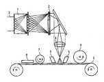
- the drawingshows an embodiment of a system for laser structuring of functional polymers in a roll-to-roll process together with other devices for producing and treating layers.
- a laser 1with optics.
- lasersare used which emit in the ultraviolet spectral region (ca 100 to 350 nm).
- the laseris an excimer laser.
- the opticsserve to widen the laser beam.
- Laser beam 3then passes through mask 2 .
- the image of a mask 2 in the optical path 3ensures that not the complete layer of functional polymer but rather specific areas thereof are removed so that precisely the desired shape of the electrodes or conducting paths remains.
- the laser beamhas preferably a greater cross-section at the mask so as to protect the mask from being damaged. For this reason, optics 4 are required so that a reduced image of the mask is projected onto the layer of functional polymer.
- Optics 4guide the beam onto the substrate roll 9 to be structured, eg, a coated substrate. Now the action of the laser beam 3 causes part of a layer of functional polymer disposed on the substrate roll 9 to be locally removed. The functional polymer remaining on the substrate roll 9 then forms, say, electrodes and/or conducting paths, etc., when the functional polymer is a conductive functional polymer. The functional polymer is removed as in a dry etching process.
- the system outlinedcontains a suction device 5 , since it is to be expected that the laser ablation will produce degradation products.
- the device 6may be, say, a coating unit that produces a complete layer, which is then laser-structured.
- the device 7can be, say, a printing unit that applies another structured layer by a printing process. It may then be necessary, under certain circumstances, to dry the printed layer, for which purpose drying equipment 8 is proposed.
- the embodiment showncan be arbitrarily modified and expanded, and, in particular, it is conceivable to operate with a number of in-line and/or parallel laser structuring steps.
- a first lasermight effect electrode structuring
- a second lasercould produce the through-connections (via holes).
- Laser structuringcombines two advantages. Firstly, as shown above, it is roll-to-roll compatible and thus allows for maximum production rates. Secondly, it has a very high resolving power. At present there exists no other process for semiconductor structuring that combines these two advantages, neither photolithography nor printing processes nor any other methods. Furthermore, laser structuring can be combined with other roll-to-roll processes such as printing processes.
Landscapes
- Engineering & Computer Science (AREA)
- Physics & Mathematics (AREA)
- Optics & Photonics (AREA)
- Manufacturing & Machinery (AREA)
- Plasma & Fusion (AREA)
- Mechanical Engineering (AREA)
- Laser Beam Processing (AREA)
- Manufacturing Of Printed Wiring (AREA)
- Formation Of Insulating Films (AREA)
Abstract
Description
- The invention relates to a device and process for laser structuring and applications thereof in the production of semiconductors.
- Essentially two methods are known for structuring organic functional polymers: photo-lithography, which necessitates piece-by-piece processing, and continuous printing processes.
- DE 100 33 112, DE 100 43 204 and DE 100 61 297 disclose continuous printing processes for structuring organic functional polymers. However, these fast printing processes are as yet unable to achieve the high resolution obtainable using photolithographic structuring methods.
- It is therefore an object of the invention to provide a process for continuous structuring of functional polymers, in which high structuring resolution can be achieved despite a high throughput rate of the functional polymer.
- The present invention relates to a device for structuring a functional polymer, comprising at least one continuously moving web carrying a coated substrate, at least one laser and at least one mask situated between the laser and the substrate, laser, mask and substrate being disposed such that the coated substrate is bombarded by the laser through the mask such that the layer on the substrate is removed locally therefrom in conformity with the configuration of the mask. Another object of the invention is to provide a process for structuring functional polymers by means of at least one laser ablation step, in which, in a continuous working process, the image of said mask is projected by at least one laser pulse onto at least one continuous substrate coated with at least one functional polymer such that the functional polymer is locally removed in conformity with the configuration of said mask.
- Finally, further objects of the invention are various applications relating to processes for the production of integrated circuits.
- By “functional polymer” we mean an organic material that fulfils a function in a semi-conductor component (ie conductivity, non-conductivity, semi-conductivity, transparence, opacity, and/or insulation) or a combination of two or more functions.
- The term “organic material” or “functional polymer” or “polymer” includes in this case all types of organic, organometallic, and/or organic-inorganic man-made materials (hybrids), particularly those referred to in the English language as, eg, “plastics”. All types of materials are suitable with the exception of the semiconductors forming classical diodes (germanium, silicon) and the typical metallic conductors. It is thus not intended to dogmatically confine organic material to that consisting of purely carbonaceous material, but rather the term also covers the wide use of, say, silicones. Furthermore, the term should not, with respect to molecular size, be particularly confined to polymeric and/or oligomeric materials but can also refer to the use of “small molecules”. The word component “polymer” in the term “functional polymer” is of historical origin and contains no inference to the presence of an actual polymeric compound,
- The process of laser ablation as a method for the manufacture of structured layers of functional polymer is a direct lithographic process, in which laser bombardment combines both the effect of structuring by exposure and the dry etching process of the conventional photolithographic process. Laser structuring has hitherto been known only in conjunction with piece-by-piece processing in the production of semiconductors. According to the invention, the image of a mask is simultaneously projected onto the layer to be structured in a manner similar to that employed in photo-lithography.
- The invention makes it possible, for the first time, to make use of laser ablation, ie the local removal of polymeric material due to laser bombardment, in a continuous process for the production of semiconductors.
- Advantageously, the continuous process employed is a roller-to-roller process, in which a web carrying a coated substrate (substrate roll) is subjected at high speed to process steps such as printing, coating, etc., without having to stop for the ablation step.
- In an advantageous embodiment, laser ablation is effected by a single laser pulse.
- A single laser pulse of approximately 20 ns is so short that it produces sharp images even when the web travels at maximum speed, eg, 20 m/s. In the numerical example given here, the degree of unsharpness caused by the motion of the web is less than 1 nm. This is negligible compared with the desired structure sizes in the micron range.
- This makes it clear that laser structuring is basically compatible with roll-to-roll processes. For the sake of clarification, it might be mentioned that the present process does not involve the frequently used sequential writing using a focused laser beam, which has its limits as regards speed and resolution, but involves laser pulses, which means that, in a manner similar to photolithography, the image of a mask is simultaneously projected onto the layer to be structured so that each laser pulse produces a complete integrated circuit.
- According to one embodiment, the image of the mask is reduced by a factor of 5. In other words, the mask is typically 5 times larger than its projected image in order to decrease the power density in the mask, as otherwise the mask would itself be ablated.
- According to one embodiment, laser ablation is combined with at least one suction device.
- The process can replace all of the process steps involved in stereolithography during the production of semiconductors. In particular, the process can be used for:
- Laser structuring electrodes (source/drain and gate) in organic field effect transistors.
- These electrodes can comprise metals (eg, gold, aluminum, copper) or conductive polymers (eg, polyaniline and PEDOT/PSS, polypyrrole, polyacetylene, etc.) or other conductive, particularly organic, materials or composite materials (eg, conductive lamp black and pastes containing metals (eg, conductive silver)). For example the following conductive polymers are capably of being structured using laser: polyaniline (PANI); poly-3,4-ethylenedioxythiophene (PEDOT); polypyrrole (Ppy).
- For source/drain electrodes it has been possible to achieve structure sizes down to 1 μm. In addition, ablation experiments on laminates have already been carried out.
- The object of the procedure is to remove only the top layer without attacking the underlying layer. This can be achieved by adjusting the energy or power of the laser pulse, the wavelength of the laser light and the number of laser pulses. This is an important factor when structuring the gate electrode forming the top layer of the transistor structure.
- Structuring of semiconductor and/or insulator layers. Examples of organic semiconductors are: polythiophenes, polyfluorenes, pentacene, perylene, etc. An example of an organic insulator is poly-4-vinylphenol or polyhydroxystyrene.
- The production of through-connections (via holes) in organic transistors. In a transistor the electrodes (source/drain and gate) are separated from each other by the intermediate semiconductor and insulator layers. A connection between these two, as is necessary for the production of integrated circuits, can likewise be effected by laser structuring, ie by local pinpoint removal of the semiconductor and insulator layers followed by filling the hole with a conductive material,
- Further applications of the process for the production of organic circuits are:
- conducting paths, contact pads, resistors, electrodes, semi-conducting layers, insulator layers for other electronic organic components, eg, for condensers, organic diode structures or organic photovoltaic structures.
- The invention is explained below with reference to the drawing:
- The drawing shows an embodiment of a system for laser structuring of functional polymers in a roll-to-roll process together with other devices for producing and treating layers. It shows a
laser 1 with optics. Preferably, lasers are used which emit in the ultraviolet spectral region (ca 100 to 350 nm). Typically, the laser is an excimer laser. The optics serve to widen the laser beam. Laser beam3 then passes through mask2. The image of a mask2 in the optical path3 ensures that not the complete layer of functional polymer but rather specific areas thereof are removed so that precisely the desired shape of the electrodes or conducting paths remains. The laser beam has preferably a greater cross-section at the mask so as to protect the mask from being damaged. For this reason, optics4 are required so that a reduced image of the mask is projected onto the layer of functional polymer. - Optics4 guide the beam onto the
substrate roll 9 to be structured, eg, a coated substrate. Now the action of the laser beam3 causes part of a layer of functional polymer disposed on thesubstrate roll 9 to be locally removed. The functional polymer remaining on thesubstrate roll 9 then forms, say, electrodes and/or conducting paths, etc., when the functional polymer is a conductive functional polymer. The functional polymer is removed as in a dry etching process. The system outlined contains asuction device 5, since it is to be expected that the laser ablation will produce degradation products. - Furthermore, there are provided before and after the laser ablation area, as regarded in the direction of travel of the substrate, devices for the production and treatment of a
coating 6 and/orprinting devices 7. Thus thedevice 6 may be, say, a coating unit that produces a complete layer, which is then laser-structured. Thedevice 7 can be, say, a printing unit that applies another structured layer by a printing process. It may then be necessary, under certain circumstances, to dry the printed layer, for whichpurpose drying equipment 8 is proposed. The embodiment shown can be arbitrarily modified and expanded, and, in particular, it is conceivable to operate with a number of in-line and/or parallel laser structuring steps. Thus a first laser might effect electrode structuring, whilst, after the application of another layer, a second laser could produce the through-connections (via holes). - Laser structuring combines two advantages. Firstly, as shown above, it is roll-to-roll compatible and thus allows for maximum production rates. Secondly, it has a very high resolving power. At present there exists no other process for semiconductor structuring that combines these two advantages, neither photolithography nor printing processes nor any other methods. Furthermore, laser structuring can be combined with other roll-to-roll processes such as printing processes.
Claims (9)
1. A device for structuring a functional polymer, comprising at least one continuously moving web carrying a coated substrate, the coating forming a layer on the substrate, at least one laser for generating a beam and a mask, the laser, mask and substrate being disposed such that said coated substrate is bombarded by said laser beam through said mask such that the layer on said substrate is removed locally therefrom in conformity with the configuration of said mask.
2. A device as defined inclaim 1 , wherein said laser emits the beam in the ultraviolet spectral region.
3. A device as defined in any one of the previous claims, wherein said laser is an excimer laser.
4. A device as defined in any one of claims1 and2, including a suction device for removing debris from said substrate.
5. A process for structuring functional polymers by at least one laser ablation step, wherein, in a continuous working process, the image of a mask is projected by at least one laser pulse onto a continuous substrate coated with at least one functional polymer such that said functional polymer is locally removed in conformity with the configuration of said mask.
6. A process as defined inclaim 5 , wherein said continuous working process is a roller-to-roller process.
7. a process as defined inclaim 5 orclaim 6 , wherein said laser ablation is effected by a single laser pulse.
8. A process as defined in any one of claims5 or6, wherein the projected image of said mask is reduced by a factor of 5.
9. A method of using a device as defined in any one of claims1 or2 and/or of using a process as defined in any one of claims5 or6 for laser structuring electrodes, for structuring semiconductor and/or insulator layers, for making through-connections (via holes) of organic transistors and/or for the production of conducting paths, contact pads, resistors, electrodes, semi-conducting layers, insulator layers for electronic and/or electrical components, for condensers, organic diode structures, or organic photovoltaic structures.
Applications Claiming Priority (3)
| Application Number | Priority Date | Filing Date | Title |
|---|---|---|---|
| DE10212639ADE10212639A1 (en) | 2002-03-21 | 2002-03-21 | Device and method for laser structuring functional polymers and uses |
| DE10212639.9 | 2002-03-21 | ||
| PCT/DE2003/000791WO2003080285A1 (en) | 2002-03-21 | 2003-03-12 | Device and method for laser structuring functional polymers and the uses thereof |
Publications (1)
| Publication Number | Publication Date |
|---|---|
| US20050106507A1true US20050106507A1 (en) | 2005-05-19 |
Family
ID=28050742
Family Applications (1)
| Application Number | Title | Priority Date | Filing Date |
|---|---|---|---|
| US10/508,737AbandonedUS20050106507A1 (en) | 2002-03-21 | 2003-03-12 | Device and method for laser structuring functional polymers and the use thereof |
Country Status (4)
| Country | Link |
|---|---|
| US (1) | US20050106507A1 (en) |
| EP (1) | EP1487605B1 (en) |
| DE (2) | DE10212639A1 (en) |
| WO (1) | WO2003080285A1 (en) |
Cited By (13)
| Publication number | Priority date | Publication date | Assignee | Title |
|---|---|---|---|---|
| US20030183817A1 (en)* | 2000-09-01 | 2003-10-02 | Adolf Bernds | Organic field effect transistor, method for structuring an ofet and integrated circuit |
| WO2006129126A2 (en) | 2005-06-01 | 2006-12-07 | Plastic Logic Limited | Layer-selective laser ablation patterning |
| WO2007110671A3 (en)* | 2006-03-29 | 2007-12-21 | Plastic Logic Ltd | Techniques for device fabrication with self-aligned electrodes |
| JP2009508321A (en)* | 2005-06-01 | 2009-02-26 | プラスティック ロジック リミテッド | Layer selective laser ablation patterning |
| US20090166812A1 (en)* | 2006-02-23 | 2009-07-02 | Picodeon Ltd Oy | Semiconductor and an arrangement and a method for producing a semiconductor |
| EP2102906A1 (en)* | 2006-12-14 | 2009-09-23 | Plastic Logic Limited | Elimination of short circuits between conductors by laser ablation |
| US20100201038A1 (en)* | 2007-01-19 | 2010-08-12 | Basf Se | Method for the transfer of structural data, and device therefor |
| US20100227434A1 (en)* | 2008-12-23 | 2010-09-09 | Cambridge Display Technology Ltd. | Method of Fabricating a Self-aligned Top-gate Organic Transistor |
| KR101353434B1 (en) | 2011-10-17 | 2014-01-21 | 주식회사 엘지화학 | Substrate for organic electronic device |
| US20140054065A1 (en)* | 2012-08-21 | 2014-02-27 | Abner D. Joseph | Electrical circuit trace manufacturing for electro-chemical sensors |
| US10369565B2 (en) | 2014-12-31 | 2019-08-06 | Abbott Laboratories | Digital microfluidic dilution apparatus, systems, and related methods |
| US10913064B2 (en) | 2014-04-16 | 2021-02-09 | Abbott Laboratories | Droplet actuator fabrication apparatus, systems, and related methods |
| JP2022023055A (en)* | 2013-12-02 | 2022-02-07 | 株式会社半導体エネルギー研究所 | How to use the linear beam irradiation device |
Families Citing this family (11)
| Publication number | Priority date | Publication date | Assignee | Title |
|---|---|---|---|---|
| DE602005025074D1 (en) | 2004-12-08 | 2011-01-13 | Samsung Mobile Display Co Ltd | Method for producing a conductor structure of a thin-film transistor |
| GB0506896D0 (en)* | 2005-04-05 | 2005-05-11 | Plastic Logic Ltd | Stack ablation |
| KR100647690B1 (en) | 2005-04-22 | 2006-11-23 | 삼성에스디아이 주식회사 | Thin film transistor and flat panel display device having same |
| KR100647695B1 (en) | 2005-05-27 | 2006-11-23 | 삼성에스디아이 주식회사 | Organic thin film transistor, manufacturing method thereof and flat panel display device having same |
| US7176053B1 (en) | 2005-08-16 | 2007-02-13 | Organicid, Inc. | Laser ablation method for fabricating high performance organic devices |
| DE102007016638A1 (en)* | 2007-01-31 | 2008-08-07 | Osram Opto Semiconductors Gmbh | Process for structuring electroluminescent organic semiconductor elements, electroluminescent organic semiconductor element and arrangement for structuring such an element |
| DE102007034644A1 (en) | 2007-07-23 | 2009-01-29 | Thüringisches Institut für Textil- und Kunststoff-Forschung e.V. | Method and device for laser structuring of solar cells |
| US20090155963A1 (en)* | 2007-12-12 | 2009-06-18 | Hawkins Gilbert A | Forming thin film transistors using ablative films |
| DE102008015697A1 (en)* | 2008-03-26 | 2009-10-01 | Osram Opto Semiconductors Gmbh | Structured opto-electronic element e.g. bottom emitter, producing method for organic LED, involves structuring layer from charge carrier injection layers, and radiation-emitting layer by irradiating layer with electromagnetic radiation |
| DE102011101585B4 (en)* | 2011-05-12 | 2015-11-12 | Technische Universität Dresden | Process for the production of light-emitting diodes or photovoltaic elements |
| EP3568432B1 (en) | 2017-01-11 | 2024-03-20 | SHPP Global Technologies B.V. | Composition with thermal conductivity and laser plating performance by core-shell structure lds additive with metal compounds coated on mineral filler surface |
Citations (76)
| Publication number | Priority date | Publication date | Assignee | Title |
|---|---|---|---|---|
| US3512052A (en)* | 1968-01-11 | 1970-05-12 | Gen Motors Corp | Metal-insulator-semiconductor voltage variable capacitor with controlled resistivity dielectric |
| US3769096A (en)* | 1971-03-12 | 1973-10-30 | Bell Telephone Labor Inc | Pyroelectric devices |
| US3955098A (en)* | 1973-10-12 | 1976-05-04 | Hitachi, Ltd. | Switching circuit having floating gate mis load transistors |
| US4302648A (en)* | 1978-01-26 | 1981-11-24 | Shin-Etsu Polymer Co., Ltd. | Key-board switch unit |
| US4340657A (en)* | 1980-02-19 | 1982-07-20 | Polychrome Corporation | Novel radiation-sensitive articles |
| US4442019A (en)* | 1978-05-26 | 1984-04-10 | Marks Alvin M | Electroordered dipole suspension |
| US4865197A (en)* | 1988-03-04 | 1989-09-12 | Unisys Corporation | Electronic component transportation container |
| US4926052A (en)* | 1986-03-03 | 1990-05-15 | Kabushiki Kaisha Toshiba | Radiation detecting device |
| US4937119A (en)* | 1988-12-15 | 1990-06-26 | Hoechst Celanese Corp. | Textured organic optical data storage media and methods of preparation |
| US5173835A (en)* | 1991-10-15 | 1992-12-22 | Motorola, Inc. | Voltage variable capacitor |
| US5206525A (en)* | 1989-12-27 | 1993-04-27 | Nippon Petrochemicals Co., Ltd. | Electric element capable of controlling the electric conductivity of π-conjugated macromolecular materials |
| US5259926A (en)* | 1991-09-24 | 1993-11-09 | Hitachi, Ltd. | Method of manufacturing a thin-film pattern on a substrate |
| US5321240A (en)* | 1992-01-30 | 1994-06-14 | Mitsubishi Denki Kabushiki Kaisha | Non-contact IC card |
| US5347144A (en)* | 1990-07-04 | 1994-09-13 | Centre National De La Recherche Scientifique (Cnrs) | Thin-layer field-effect transistors with MIS structure whose insulator and semiconductor are made of organic materials |
| US5364735A (en)* | 1988-07-01 | 1994-11-15 | Sony Corporation | Multiple layer optical record medium with protective layers and method for producing same |
| US5395504A (en)* | 1993-02-04 | 1995-03-07 | Asulab S.A. | Electrochemical measuring system with multizone sensors |
| US5486851A (en)* | 1991-10-30 | 1996-01-23 | Fraunhofer-Gesellschaft Zur Forderung Der Angewandten Forschung E.V. | Illumination device using a pulsed laser source a Schlieren optical system and a matrix addressable surface light modulator for producing images with undifracted light |
| US5494781A (en)* | 1993-08-26 | 1996-02-27 | Matsushita Electric Works, Ltd. | Method for manufacturing printed circuit board |
| US5502396A (en)* | 1993-09-21 | 1996-03-26 | Asulab S.A. | Measuring device with connection for a removable sensor |
| US5569879A (en)* | 1991-02-19 | 1996-10-29 | Gemplus Card International | Integrated circuit micromodule obtained by the continuous assembly of patterned strips |
| US5574291A (en)* | 1994-12-09 | 1996-11-12 | Lucent Technologies Inc. | Article comprising a thin film transistor with low conductivity organic layer |
| US5580794A (en)* | 1993-08-24 | 1996-12-03 | Metrika Laboratories, Inc. | Disposable electronic assay device |
| US5625199A (en)* | 1996-01-16 | 1997-04-29 | Lucent Technologies Inc. | Article comprising complementary circuit with inorganic n-channel and organic p-channel thin film transistors |
| US5629530A (en)* | 1994-05-16 | 1997-05-13 | U.S. Phillips Corporation | Semiconductor device having an organic semiconductor material |
| US5630986A (en)* | 1995-01-13 | 1997-05-20 | Bayer Corporation | Dispensing instrument for fluid monitoring sensors |
| US5652645A (en)* | 1995-07-24 | 1997-07-29 | Anvik Corporation | High-throughput, high-resolution, projection patterning system for large, flexible, roll-fed, electronic-module substrates |
| US5691089A (en)* | 1993-03-25 | 1997-11-25 | Texas Instruments Incorporated | Integrated circuits formed in radiation sensitive material and method of forming same |
| US5705826A (en)* | 1994-06-28 | 1998-01-06 | Hitachi, Ltd. | Field-effect transistor having a semiconductor layer made of an organic compound |
| US5729428A (en)* | 1995-04-25 | 1998-03-17 | Nec Corporation | Solid electrolytic capacitor with conductive polymer as solid electrolyte and method for fabricating the same |
| US5869972A (en)* | 1996-02-26 | 1999-02-09 | Birch; Brian Jeffrey | Testing device using a thermochromic display and method of using same |
| US5883397A (en)* | 1993-07-01 | 1999-03-16 | Mitsubishi Denki Kabushiki Kaisha | Plastic functional element |
| US5892244A (en)* | 1989-01-10 | 1999-04-06 | Mitsubishi Denki Kabushiki Kaisha | Field effect transistor including πconjugate polymer and liquid crystal display including the field effect transistor |
| US5946551A (en)* | 1997-03-25 | 1999-08-31 | Dimitrakopoulos; Christos Dimitrios | Fabrication of thin film effect transistor comprising an organic semiconductor and chemical solution deposited metal oxide gate dielectric |
| US5970318A (en)* | 1997-05-15 | 1999-10-19 | Electronics And Telecommunications Research Institute | Fabrication method of an organic electroluminescent devices |
| US5973598A (en)* | 1997-09-11 | 1999-10-26 | Precision Dynamics Corporation | Radio frequency identification tag on flexible substrate |
| US5994773A (en)* | 1996-03-06 | 1999-11-30 | Hirakawa; Tadashi | Ball grid array semiconductor package |
| US5998805A (en)* | 1997-12-11 | 1999-12-07 | Motorola, Inc. | Active matrix OED array with improved OED cathode |
| US5997817A (en)* | 1997-12-05 | 1999-12-07 | Roche Diagnostics Corporation | Electrochemical biosensor test strip |
| US6036919A (en)* | 1996-07-23 | 2000-03-14 | Roche Diagnostic Gmbh | Diagnostic test carrier with multilayer field |
| US6045977A (en)* | 1998-02-19 | 2000-04-04 | Lucent Technologies Inc. | Process for patterning conductive polyaniline films |
| US6072716A (en)* | 1999-04-14 | 2000-06-06 | Massachusetts Institute Of Technology | Memory structures and methods of making same |
| US6087196A (en)* | 1998-01-30 | 2000-07-11 | The Trustees Of Princeton University | Fabrication of organic semiconductor devices using ink jet printing |
| US6133835A (en)* | 1997-12-05 | 2000-10-17 | U.S. Philips Corporation | Identification transponder |
| US6150668A (en)* | 1998-05-29 | 2000-11-21 | Lucent Technologies Inc. | Thin-film transistor monolithically integrated with an organic light-emitting diode |
| US6197663B1 (en)* | 1999-12-07 | 2001-03-06 | Lucent Technologies Inc. | Process for fabricating integrated circuit devices having thin film transistors |
| US6207472B1 (en)* | 1999-03-09 | 2001-03-27 | International Business Machines Corporation | Low temperature thin film transistor fabrication |
| US6221553B1 (en)* | 1999-01-15 | 2001-04-24 | 3M Innovative Properties Company | Thermal transfer element for forming multilayer devices |
| US20010006766A1 (en)* | 1999-01-14 | 2001-07-05 | 3M Innovative Properties Company | Method for patterning thin films |
| US6300141B1 (en)* | 1999-03-02 | 2001-10-09 | Helix Biopharma Corporation | Card-based biosensor device |
| US6321571B1 (en)* | 1998-12-21 | 2001-11-27 | Corning Incorporated | Method of making glass structures for flat panel displays |
| US6330434B1 (en)* | 1997-11-27 | 2001-12-11 | Nec Corporation | Mobile communication system capable of being connected to wireless line only during actual data communication |
| US6329226B1 (en)* | 2000-06-01 | 2001-12-11 | Agere Systems Guardian Corp. | Method for fabricating a thin-film transistor |
| US6344662B1 (en)* | 1997-03-25 | 2002-02-05 | International Business Machines Corporation | Thin-film field-effect transistor with organic-inorganic hybrid semiconductor requiring low operating voltages |
| US20020018911A1 (en)* | 1999-05-11 | 2002-02-14 | Mark T. Bernius | Electroluminescent or photocell device having protective packaging |
| US6362509B1 (en)* | 1999-10-11 | 2002-03-26 | U.S. Philips Electronics | Field effect transistor with organic semiconductor layer |
| US6384804B1 (en)* | 1998-11-25 | 2002-05-07 | Lucent Techonologies Inc. | Display comprising organic smart pixels |
| US20020053320A1 (en)* | 1998-12-15 | 2002-05-09 | Gregg M. Duthaler | Method for printing of transistor arrays on plastic substrates |
| US20020056839A1 (en)* | 2000-11-11 | 2002-05-16 | Pt Plus Co. Ltd. | Method of crystallizing a silicon thin film and semiconductor device fabricated thereby |
| US20020068392A1 (en)* | 2000-12-01 | 2002-06-06 | Pt Plus Co. Ltd. | Method for fabricating thin film transistor including crystalline silicon active layer |
| US6403396B1 (en)* | 1998-01-28 | 2002-06-11 | Thin Film Electronics Asa | Method for generation of electrically conducting or semiconducting structures in three dimensions and methods for erasure of the same structures |
| US6429450B1 (en)* | 1997-08-22 | 2002-08-06 | Koninklijke Philips Electronics N.V. | Method of manufacturing a field-effect transistor substantially consisting of organic materials |
| US20020130042A1 (en)* | 2000-03-02 | 2002-09-19 | Moerman Piet H.C. | Combined lancet and electrochemical analyte-testing apparatus |
| US20020170897A1 (en)* | 2001-05-21 | 2002-11-21 | Hall Frank L. | Methods for preparing ball grid array substrates via use of a laser |
| US6498114B1 (en)* | 1999-04-09 | 2002-12-24 | E Ink Corporation | Method for forming a patterned semiconductor film |
| US20020195644A1 (en)* | 2001-06-08 | 2002-12-26 | Ananth Dodabalapur | Organic polarizable gate transistor apparatus and method |
| US6555840B1 (en)* | 1999-02-16 | 2003-04-29 | Sharp Kabushiki Kaisha | Charge-transport structures |
| US20030112576A1 (en)* | 2001-09-28 | 2003-06-19 | Brewer Peter D. | Process for producing high performance interconnects |
| US6593690B1 (en)* | 1999-09-03 | 2003-07-15 | 3M Innovative Properties Company | Large area organic electronic devices having conducting polymer buffer layers and methods of making same |
| US20030141807A1 (en)* | 2001-01-31 | 2003-07-31 | Takeo Kawase | Display device |
| US6603139B1 (en)* | 1998-04-16 | 2003-08-05 | Cambridge Display Technology Limited | Polymer devices |
| US6621098B1 (en)* | 1999-11-29 | 2003-09-16 | The Penn State Research Foundation | Thin-film transistor and methods of manufacturing and incorporating a semiconducting organic material |
| US20040002176A1 (en)* | 2002-06-28 | 2004-01-01 | Xerox Corporation | Organic ferroelectric memory cells |
| US20040084670A1 (en)* | 2002-11-04 | 2004-05-06 | Tripsas Nicholas H. | Stacked organic memory devices and methods of operating and fabricating |
| US6852583B2 (en)* | 2000-07-07 | 2005-02-08 | Siemens Aktiengesellschaft | Method for the production and configuration of organic field-effect transistors (OFET) |
| US6903958B2 (en)* | 2000-09-13 | 2005-06-07 | Siemens Aktiengesellschaft | Method of writing to an organic memory |
| US7229868B2 (en)* | 2000-12-08 | 2007-06-12 | Polyic Gmbh & Co. Kg | Organic field-effect transistor, method for structuring an OFET and integrated circuit |
Family Cites Families (1)
| Publication number | Priority date | Publication date | Assignee | Title |
|---|---|---|---|---|
| US6888096B1 (en)* | 1999-09-28 | 2005-05-03 | Sumitomo Heavy Industries, Ltd. | Laser drilling method and laser drilling device |
- 2002
- 2002-03-21DEDE10212639Apatent/DE10212639A1/ennot_activeCeased
- 2003
- 2003-03-12WOPCT/DE2003/000791patent/WO2003080285A1/enactiveIP Right Grant
- 2003-03-12EPEP03711841Apatent/EP1487605B1/ennot_activeExpired - Lifetime
- 2003-03-12USUS10/508,737patent/US20050106507A1/ennot_activeAbandoned
- 2003-03-12DEDE50308846Tpatent/DE50308846D1/ennot_activeExpired - Lifetime
Patent Citations (78)
| Publication number | Priority date | Publication date | Assignee | Title |
|---|---|---|---|---|
| US3512052A (en)* | 1968-01-11 | 1970-05-12 | Gen Motors Corp | Metal-insulator-semiconductor voltage variable capacitor with controlled resistivity dielectric |
| US3769096A (en)* | 1971-03-12 | 1973-10-30 | Bell Telephone Labor Inc | Pyroelectric devices |
| US3955098A (en)* | 1973-10-12 | 1976-05-04 | Hitachi, Ltd. | Switching circuit having floating gate mis load transistors |
| US4302648A (en)* | 1978-01-26 | 1981-11-24 | Shin-Etsu Polymer Co., Ltd. | Key-board switch unit |
| US4442019A (en)* | 1978-05-26 | 1984-04-10 | Marks Alvin M | Electroordered dipole suspension |
| US4340657A (en)* | 1980-02-19 | 1982-07-20 | Polychrome Corporation | Novel radiation-sensitive articles |
| US4926052A (en)* | 1986-03-03 | 1990-05-15 | Kabushiki Kaisha Toshiba | Radiation detecting device |
| US4865197A (en)* | 1988-03-04 | 1989-09-12 | Unisys Corporation | Electronic component transportation container |
| US5364735A (en)* | 1988-07-01 | 1994-11-15 | Sony Corporation | Multiple layer optical record medium with protective layers and method for producing same |
| US4937119A (en)* | 1988-12-15 | 1990-06-26 | Hoechst Celanese Corp. | Textured organic optical data storage media and methods of preparation |
| US5892244A (en)* | 1989-01-10 | 1999-04-06 | Mitsubishi Denki Kabushiki Kaisha | Field effect transistor including πconjugate polymer and liquid crystal display including the field effect transistor |
| US6060338A (en)* | 1989-01-10 | 2000-05-09 | Mitsubishi Denki Kabushiki Kaisha | Method of making a field effect transistor |
| US5206525A (en)* | 1989-12-27 | 1993-04-27 | Nippon Petrochemicals Co., Ltd. | Electric element capable of controlling the electric conductivity of π-conjugated macromolecular materials |
| US5347144A (en)* | 1990-07-04 | 1994-09-13 | Centre National De La Recherche Scientifique (Cnrs) | Thin-layer field-effect transistors with MIS structure whose insulator and semiconductor are made of organic materials |
| US5569879A (en)* | 1991-02-19 | 1996-10-29 | Gemplus Card International | Integrated circuit micromodule obtained by the continuous assembly of patterned strips |
| US5259926A (en)* | 1991-09-24 | 1993-11-09 | Hitachi, Ltd. | Method of manufacturing a thin-film pattern on a substrate |
| US5173835A (en)* | 1991-10-15 | 1992-12-22 | Motorola, Inc. | Voltage variable capacitor |
| US5486851A (en)* | 1991-10-30 | 1996-01-23 | Fraunhofer-Gesellschaft Zur Forderung Der Angewandten Forschung E.V. | Illumination device using a pulsed laser source a Schlieren optical system and a matrix addressable surface light modulator for producing images with undifracted light |
| US5321240A (en)* | 1992-01-30 | 1994-06-14 | Mitsubishi Denki Kabushiki Kaisha | Non-contact IC card |
| US5395504A (en)* | 1993-02-04 | 1995-03-07 | Asulab S.A. | Electrochemical measuring system with multizone sensors |
| US5691089A (en)* | 1993-03-25 | 1997-11-25 | Texas Instruments Incorporated | Integrated circuits formed in radiation sensitive material and method of forming same |
| US5883397A (en)* | 1993-07-01 | 1999-03-16 | Mitsubishi Denki Kabushiki Kaisha | Plastic functional element |
| US5580794A (en)* | 1993-08-24 | 1996-12-03 | Metrika Laboratories, Inc. | Disposable electronic assay device |
| US5494781A (en)* | 1993-08-26 | 1996-02-27 | Matsushita Electric Works, Ltd. | Method for manufacturing printed circuit board |
| US5502396A (en)* | 1993-09-21 | 1996-03-26 | Asulab S.A. | Measuring device with connection for a removable sensor |
| US5629530A (en)* | 1994-05-16 | 1997-05-13 | U.S. Phillips Corporation | Semiconductor device having an organic semiconductor material |
| US5854139A (en)* | 1994-06-28 | 1998-12-29 | Hitachi, Ltd. | Organic field-effect transistor and production thereof |
| US5705826A (en)* | 1994-06-28 | 1998-01-06 | Hitachi, Ltd. | Field-effect transistor having a semiconductor layer made of an organic compound |
| US5574291A (en)* | 1994-12-09 | 1996-11-12 | Lucent Technologies Inc. | Article comprising a thin film transistor with low conductivity organic layer |
| US5630986A (en)* | 1995-01-13 | 1997-05-20 | Bayer Corporation | Dispensing instrument for fluid monitoring sensors |
| US5729428A (en)* | 1995-04-25 | 1998-03-17 | Nec Corporation | Solid electrolytic capacitor with conductive polymer as solid electrolyte and method for fabricating the same |
| US5652645A (en)* | 1995-07-24 | 1997-07-29 | Anvik Corporation | High-throughput, high-resolution, projection patterning system for large, flexible, roll-fed, electronic-module substrates |
| US5625199A (en)* | 1996-01-16 | 1997-04-29 | Lucent Technologies Inc. | Article comprising complementary circuit with inorganic n-channel and organic p-channel thin film transistors |
| US5869972A (en)* | 1996-02-26 | 1999-02-09 | Birch; Brian Jeffrey | Testing device using a thermochromic display and method of using same |
| US5994773A (en)* | 1996-03-06 | 1999-11-30 | Hirakawa; Tadashi | Ball grid array semiconductor package |
| US6036919A (en)* | 1996-07-23 | 2000-03-14 | Roche Diagnostic Gmbh | Diagnostic test carrier with multilayer field |
| US5946551A (en)* | 1997-03-25 | 1999-08-31 | Dimitrakopoulos; Christos Dimitrios | Fabrication of thin film effect transistor comprising an organic semiconductor and chemical solution deposited metal oxide gate dielectric |
| US6344662B1 (en)* | 1997-03-25 | 2002-02-05 | International Business Machines Corporation | Thin-film field-effect transistor with organic-inorganic hybrid semiconductor requiring low operating voltages |
| US5970318A (en)* | 1997-05-15 | 1999-10-19 | Electronics And Telecommunications Research Institute | Fabrication method of an organic electroluminescent devices |
| US6429450B1 (en)* | 1997-08-22 | 2002-08-06 | Koninklijke Philips Electronics N.V. | Method of manufacturing a field-effect transistor substantially consisting of organic materials |
| US5973598A (en)* | 1997-09-11 | 1999-10-26 | Precision Dynamics Corporation | Radio frequency identification tag on flexible substrate |
| US6330434B1 (en)* | 1997-11-27 | 2001-12-11 | Nec Corporation | Mobile communication system capable of being connected to wireless line only during actual data communication |
| US5997817A (en)* | 1997-12-05 | 1999-12-07 | Roche Diagnostics Corporation | Electrochemical biosensor test strip |
| US6133835A (en)* | 1997-12-05 | 2000-10-17 | U.S. Philips Corporation | Identification transponder |
| US5998805A (en)* | 1997-12-11 | 1999-12-07 | Motorola, Inc. | Active matrix OED array with improved OED cathode |
| US6403396B1 (en)* | 1998-01-28 | 2002-06-11 | Thin Film Electronics Asa | Method for generation of electrically conducting or semiconducting structures in three dimensions and methods for erasure of the same structures |
| US6087196A (en)* | 1998-01-30 | 2000-07-11 | The Trustees Of Princeton University | Fabrication of organic semiconductor devices using ink jet printing |
| US6045977A (en)* | 1998-02-19 | 2000-04-04 | Lucent Technologies Inc. | Process for patterning conductive polyaniline films |
| US6603139B1 (en)* | 1998-04-16 | 2003-08-05 | Cambridge Display Technology Limited | Polymer devices |
| US6150668A (en)* | 1998-05-29 | 2000-11-21 | Lucent Technologies Inc. | Thin-film transistor monolithically integrated with an organic light-emitting diode |
| US6384804B1 (en)* | 1998-11-25 | 2002-05-07 | Lucent Techonologies Inc. | Display comprising organic smart pixels |
| US20020053320A1 (en)* | 1998-12-15 | 2002-05-09 | Gregg M. Duthaler | Method for printing of transistor arrays on plastic substrates |
| US6321571B1 (en)* | 1998-12-21 | 2001-11-27 | Corning Incorporated | Method of making glass structures for flat panel displays |
| US20010006766A1 (en)* | 1999-01-14 | 2001-07-05 | 3M Innovative Properties Company | Method for patterning thin films |
| US6221553B1 (en)* | 1999-01-15 | 2001-04-24 | 3M Innovative Properties Company | Thermal transfer element for forming multilayer devices |
| US6555840B1 (en)* | 1999-02-16 | 2003-04-29 | Sharp Kabushiki Kaisha | Charge-transport structures |
| US6300141B1 (en)* | 1999-03-02 | 2001-10-09 | Helix Biopharma Corporation | Card-based biosensor device |
| US6207472B1 (en)* | 1999-03-09 | 2001-03-27 | International Business Machines Corporation | Low temperature thin film transistor fabrication |
| US6498114B1 (en)* | 1999-04-09 | 2002-12-24 | E Ink Corporation | Method for forming a patterned semiconductor film |
| US6072716A (en)* | 1999-04-14 | 2000-06-06 | Massachusetts Institute Of Technology | Memory structures and methods of making same |
| US20020018911A1 (en)* | 1999-05-11 | 2002-02-14 | Mark T. Bernius | Electroluminescent or photocell device having protective packaging |
| US6593690B1 (en)* | 1999-09-03 | 2003-07-15 | 3M Innovative Properties Company | Large area organic electronic devices having conducting polymer buffer layers and methods of making same |
| US6362509B1 (en)* | 1999-10-11 | 2002-03-26 | U.S. Philips Electronics | Field effect transistor with organic semiconductor layer |
| US6621098B1 (en)* | 1999-11-29 | 2003-09-16 | The Penn State Research Foundation | Thin-film transistor and methods of manufacturing and incorporating a semiconducting organic material |
| US6197663B1 (en)* | 1999-12-07 | 2001-03-06 | Lucent Technologies Inc. | Process for fabricating integrated circuit devices having thin film transistors |
| US20020130042A1 (en)* | 2000-03-02 | 2002-09-19 | Moerman Piet H.C. | Combined lancet and electrochemical analyte-testing apparatus |
| US6329226B1 (en)* | 2000-06-01 | 2001-12-11 | Agere Systems Guardian Corp. | Method for fabricating a thin-film transistor |
| US6852583B2 (en)* | 2000-07-07 | 2005-02-08 | Siemens Aktiengesellschaft | Method for the production and configuration of organic field-effect transistors (OFET) |
| US6903958B2 (en)* | 2000-09-13 | 2005-06-07 | Siemens Aktiengesellschaft | Method of writing to an organic memory |
| US20020056839A1 (en)* | 2000-11-11 | 2002-05-16 | Pt Plus Co. Ltd. | Method of crystallizing a silicon thin film and semiconductor device fabricated thereby |
| US20020068392A1 (en)* | 2000-12-01 | 2002-06-06 | Pt Plus Co. Ltd. | Method for fabricating thin film transistor including crystalline silicon active layer |
| US7229868B2 (en)* | 2000-12-08 | 2007-06-12 | Polyic Gmbh & Co. Kg | Organic field-effect transistor, method for structuring an OFET and integrated circuit |
| US20030141807A1 (en)* | 2001-01-31 | 2003-07-31 | Takeo Kawase | Display device |
| US20020170897A1 (en)* | 2001-05-21 | 2002-11-21 | Hall Frank L. | Methods for preparing ball grid array substrates via use of a laser |
| US20020195644A1 (en)* | 2001-06-08 | 2002-12-26 | Ananth Dodabalapur | Organic polarizable gate transistor apparatus and method |
| US20030112576A1 (en)* | 2001-09-28 | 2003-06-19 | Brewer Peter D. | Process for producing high performance interconnects |
| US20040002176A1 (en)* | 2002-06-28 | 2004-01-01 | Xerox Corporation | Organic ferroelectric memory cells |
| US20040084670A1 (en)* | 2002-11-04 | 2004-05-06 | Tripsas Nicholas H. | Stacked organic memory devices and methods of operating and fabricating |
Cited By (32)
| Publication number | Priority date | Publication date | Assignee | Title |
|---|---|---|---|---|
| US20030183817A1 (en)* | 2000-09-01 | 2003-10-02 | Adolf Bernds | Organic field effect transistor, method for structuring an ofet and integrated circuit |
| US9209400B2 (en) | 2005-06-01 | 2015-12-08 | Flexenable Limited | Layer-selective laser ablation patterning |
| WO2006129126A2 (en) | 2005-06-01 | 2006-12-07 | Plastic Logic Limited | Layer-selective laser ablation patterning |
| USRE45885E1 (en)* | 2005-06-01 | 2016-02-09 | Flexenable Limited | Laser ablation of electronic devices |
| JP2009508321A (en)* | 2005-06-01 | 2009-02-26 | プラスティック ロジック リミテッド | Layer selective laser ablation patterning |
| KR101366545B1 (en) | 2005-06-01 | 2014-02-25 | 플라스틱 로직 리미티드 | Layer-selective laser ablation patterning |
| US20090212292A1 (en)* | 2005-06-01 | 2009-08-27 | Carl Hayton | Layer-selective laser ablation patterning |
| JP2013118390A (en)* | 2005-06-01 | 2013-06-13 | Plastic Logic Ltd | Layer-selective laser ablation patterning |
| EP2463928A2 (en) | 2005-06-01 | 2012-06-13 | Plastic Logic Limited | Layer-selective laser ablation patterning |
| WO2006129126A3 (en)* | 2005-06-01 | 2009-11-12 | Plastic Logic Limited | Layer-selective laser ablation patterning |
| US20090166812A1 (en)* | 2006-02-23 | 2009-07-02 | Picodeon Ltd Oy | Semiconductor and an arrangement and a method for producing a semiconductor |
| US8741749B2 (en)* | 2006-02-23 | 2014-06-03 | Picodeon Ltd Oy | Semiconductor and an arrangement and a method for producing a semiconductor |
| US8987808B2 (en) | 2006-03-29 | 2015-03-24 | Cambridge Enterprise Limited | Thin film transistor with accurately aligned electrode patterns and electronic device(s) that include same |
| JP2009531848A (en)* | 2006-03-29 | 2009-09-03 | プラスティック ロジック リミテッド | Method for fabricating a device having a self-aligned electrode |
| US8900955B2 (en) | 2006-03-29 | 2014-12-02 | Cambridge Enterprise Limited | Thin film transistor device with accurately aligned electrode patterns |
| US20090166612A1 (en)* | 2006-03-29 | 2009-07-02 | Cain Paul A | Techniques for Device Fabrication with Self-Aligned Electrodes |
| WO2007110671A3 (en)* | 2006-03-29 | 2007-12-21 | Plastic Logic Ltd | Techniques for device fabrication with self-aligned electrodes |
| EP2102906A1 (en)* | 2006-12-14 | 2009-09-23 | Plastic Logic Limited | Elimination of short circuits between conductors by laser ablation |
| US8471172B2 (en) | 2006-12-14 | 2013-06-25 | Plastic Logic Limited | Elimination of short circuits between conductors by laser ablation |
| US20100201038A1 (en)* | 2007-01-19 | 2010-08-12 | Basf Se | Method for the transfer of structural data, and device therefor |
| US8546179B2 (en) | 2008-12-23 | 2013-10-01 | Cambridge Display Technology Ltd. | Method of fabricating a self-aligned top-gate organic transistor |
| US20100227434A1 (en)* | 2008-12-23 | 2010-09-09 | Cambridge Display Technology Ltd. | Method of Fabricating a Self-aligned Top-gate Organic Transistor |
| KR101353434B1 (en) | 2011-10-17 | 2014-01-21 | 주식회사 엘지화학 | Substrate for organic electronic device |
| US20140054065A1 (en)* | 2012-08-21 | 2014-02-27 | Abner D. Joseph | Electrical circuit trace manufacturing for electro-chemical sensors |
| JP2022023055A (en)* | 2013-12-02 | 2022-02-07 | 株式会社半導体エネルギー研究所 | How to use the linear beam irradiation device |
| JP7113127B2 (en) | 2013-12-02 | 2022-08-04 | 株式会社半導体エネルギー研究所 | How to use the linear beam irradiation device |
| US11672148B2 (en) | 2013-12-02 | 2023-06-06 | Semiconductor Energy Laboratory Co., Ltd. | Display device and method for manufacturing the same |
| US12048207B2 (en) | 2013-12-02 | 2024-07-23 | Semiconductor Energy Laboratory Co., Ltd. | Display device and method for manufacturing the same |
| US10913064B2 (en) | 2014-04-16 | 2021-02-09 | Abbott Laboratories | Droplet actuator fabrication apparatus, systems, and related methods |
| US12201980B2 (en) | 2014-04-16 | 2025-01-21 | Abbott Laboratories | Droplet actuator fabrication apparatus, systems, and related methods |
| US10369565B2 (en) | 2014-12-31 | 2019-08-06 | Abbott Laboratories | Digital microfluidic dilution apparatus, systems, and related methods |
| US11213817B2 (en) | 2014-12-31 | 2022-01-04 | Abbott Laboratories | Digital microfluidic dilution apparatus, systems, and related methods |
Also Published As
| Publication number | Publication date |
|---|---|
| EP1487605B1 (en) | 2007-12-19 |
| DE50308846D1 (en) | 2008-01-31 |
| EP1487605A1 (en) | 2004-12-22 |
| WO2003080285A1 (en) | 2003-10-02 |
| DE10212639A1 (en) | 2003-10-16 |
Similar Documents
| Publication | Publication Date | Title |
|---|---|---|
| US20050106507A1 (en) | Device and method for laser structuring functional polymers and the use thereof | |
| JP5230597B2 (en) | Electronic device with self-aligned electrodes | |
| US6927108B2 (en) | Solution-processed thin film transistor formation method | |
| KR100972920B1 (en) | Laser cutting method for assembling high performance organic devices | |
| US20160111667A1 (en) | Layer-selective laser ablation patterning | |
| US20070092637A1 (en) | Forming holes using laser energy | |
| EP1897157B1 (en) | Layer-selective laser ablation patterning | |
| JP5438273B2 (en) | Electronic device array | |
| EP1829134B1 (en) | Electrode patterning | |
| US9985207B2 (en) | Electronic devices | |
| EP1866965B1 (en) | Method of producing plurality of organic transistors using laser patterning | |
| US8684779B2 (en) | Electrode patterning | |
| Schrödner et al. | Polymer field effect transistors made by laser patterning | |
| de Vries et al. | Coating technologies for large area Organic Light Emitting Diodes (OLEDs) and Organic Photovoltaics (OPV) |
Legal Events
| Date | Code | Title | Description |
|---|---|---|---|
| AS | Assignment | Owner name:POLYC GMBH & CO. KG, GERMANY Free format text:ASSIGNMENT OF ASSIGNORS INTEREST;ASSIGNORS:BERNDS, ADOLF;CLEMENS, WOLFGANG;ROTH, HANS-KLAUS;AND OTHERS;REEL/FRAME:015403/0635;SIGNING DATES FROM 20041026 TO 20041103 | |
| AS | Assignment | Owner name:POLYIC GMBH & CO. KG, GERMANY Free format text:ASSIGNMENT OF ASSIGNORS INTEREST;ASSIGNORS:BERNDS, ADOLF;CLEMENS, WOLFGANG;ROTH, HANS-KLAUS;AND OTHERS;REEL/FRAME:018476/0256 Effective date:20041026 | |
| STCB | Information on status: application discontinuation | Free format text:ABANDONED -- FAILURE TO RESPOND TO AN OFFICE ACTION |