US20050105371A1 - Integrated circuit incorporating three-dimensional memory array with dual opposing decoder arrangement - Google Patents
Integrated circuit incorporating three-dimensional memory array with dual opposing decoder arrangementDownload PDFInfo
- Publication number
- US20050105371A1 US20050105371A1US10/774,818US77481804AUS2005105371A1US 20050105371 A1US20050105371 A1US 20050105371A1US 77481804 AUS77481804 AUS 77481804AUS 2005105371 A1US2005105371 A1US 2005105371A1
- Authority
- US
- United States
- Prior art keywords
- memory array
- integrated circuit
- recited
- wordlines
- row
- Prior art date
- Legal status (The legal status is an assumption and is not a legal conclusion. Google has not performed a legal analysis and makes no representation as to the accuracy of the status listed.)
- Granted
Links
- 230000015654memoryEffects0.000titleclaimsabstractdescription298
- 230000009977dual effectEffects0.000titleclaimsdescription6
- 239000000758substrateSubstances0.000claimsabstractdescription49
- 238000004519manufacturing processMethods0.000claimsdescription24
- 239000000463materialSubstances0.000claimsdescription24
- 238000003491arrayMethods0.000claimsdescription6
- 238000000034methodMethods0.000abstractdescription30
- 230000000873masking effectEffects0.000abstractdescription17
- 230000002093peripheral effectEffects0.000abstractdescription16
- 229910052710siliconInorganic materials0.000abstractdescription12
- 239000010703siliconSubstances0.000abstractdescription11
- XUIMIQQOPSSXEZ-UHFFFAOYSA-NSiliconChemical compound[Si]XUIMIQQOPSSXEZ-UHFFFAOYSA-N0.000abstractdescription10
- 239000004020conductorSubstances0.000description319
- 210000004027cellAnatomy0.000description207
- 230000008859changeEffects0.000description52
- 239000004065semiconductorSubstances0.000description34
- 229910021420polycrystalline siliconInorganic materials0.000description24
- 229920005591polysiliconPolymers0.000description21
- 230000008569processEffects0.000description21
- 229910052751metalInorganic materials0.000description16
- 239000002184metalSubstances0.000description16
- 238000000059patterningMethods0.000description14
- 230000015572biosynthetic processEffects0.000description11
- 238000005530etchingMethods0.000description10
- 230000008901benefitEffects0.000description9
- 238000000151depositionMethods0.000description9
- 230000008021depositionEffects0.000description9
- 229910021417amorphous siliconInorganic materials0.000description7
- 230000006870functionEffects0.000description7
- 239000012212insulatorSubstances0.000description7
- 230000002441reversible effectEffects0.000description7
- 238000005516engineering processMethods0.000description6
- 239000000047productSubstances0.000description6
- VYPSYNLAJGMNEJ-UHFFFAOYSA-NSilicium dioxideChemical compoundO=[Si]=OVYPSYNLAJGMNEJ-UHFFFAOYSA-N0.000description5
- 238000010586diagramMethods0.000description5
- 230000008520organizationEffects0.000description5
- 229910052782aluminiumInorganic materials0.000description4
- XAGFODPZIPBFFR-UHFFFAOYSA-NaluminiumChemical compound[Al]XAGFODPZIPBFFR-UHFFFAOYSA-N0.000description4
- 239000013078crystalSubstances0.000description4
- 238000007667floatingMethods0.000description4
- 230000002427irreversible effectEffects0.000description4
- 150000002739metalsChemical class0.000description4
- 229910021424microcrystalline siliconInorganic materials0.000description4
- 210000002381plasmaAnatomy0.000description4
- 238000005498polishingMethods0.000description4
- 230000004913activationEffects0.000description3
- 230000002457bidirectional effectEffects0.000description3
- 238000002425crystallisationMethods0.000description3
- 230000008025crystallizationEffects0.000description3
- 230000003247decreasing effectEffects0.000description3
- 230000003252repetitive effectEffects0.000description3
- 230000005355Hall effectEffects0.000description2
- 230000004888barrier functionEffects0.000description2
- 239000003990capacitorSubstances0.000description2
- 239000010406cathode materialSubstances0.000description2
- 238000005520cutting processMethods0.000description2
- 230000002950deficientEffects0.000description2
- 238000007599dischargingMethods0.000description2
- 239000002019doping agentSubstances0.000description2
- 230000000694effectsEffects0.000description2
- 239000007772electrode materialSubstances0.000description2
- 230000005669field effectEffects0.000description2
- 239000010408filmSubstances0.000description2
- 239000007943implantSubstances0.000description2
- 239000011810insulating materialSubstances0.000description2
- 238000009413insulationMethods0.000description2
- 230000010354integrationEffects0.000description2
- 230000002452interceptive effectEffects0.000description2
- 238000005468ion implantationMethods0.000description2
- 150000002500ionsChemical class0.000description2
- 238000004518low pressure chemical vapour depositionMethods0.000description2
- 230000003647oxidationEffects0.000description2
- 238000007254oxidation reactionMethods0.000description2
- 238000000206photolithographyMethods0.000description2
- 229920002120photoresistant polymerPolymers0.000description2
- 238000005240physical vapour depositionMethods0.000description2
- 238000000623plasma-assisted chemical vapour depositionMethods0.000description2
- 230000010287polarizationEffects0.000description2
- 230000009467reductionEffects0.000description2
- 229910021332silicideInorganic materials0.000description2
- 235000012239silicon dioxideNutrition0.000description2
- 239000000377silicon dioxideSubstances0.000description2
- 239000007790solid phaseSubstances0.000description2
- 239000000126substanceSubstances0.000description2
- 239000010409thin filmSubstances0.000description2
- 238000000038ultrahigh vacuum chemical vapour depositionMethods0.000description2
- 206010010144Completed suicideDiseases0.000description1
- 208000032750Device leakageDiseases0.000description1
- 229910001218Gallium arsenideInorganic materials0.000description1
- ZOKXTWBITQBERF-UHFFFAOYSA-NMolybdenumChemical compound[Mo]ZOKXTWBITQBERF-UHFFFAOYSA-N0.000description1
- 229910000577Silicon-germaniumInorganic materials0.000description1
- NRTOMJZYCJJWKI-UHFFFAOYSA-NTitanium nitrideChemical compound[Ti]#NNRTOMJZYCJJWKI-UHFFFAOYSA-N0.000description1
- 239000000654additiveSubstances0.000description1
- 230000000996additive effectEffects0.000description1
- 239000010405anode materialSubstances0.000description1
- QVGXLLKOCUKJST-UHFFFAOYSA-Natomic oxygenChemical compound[O]QVGXLLKOCUKJST-UHFFFAOYSA-N0.000description1
- 230000006399behaviorEffects0.000description1
- 239000007795chemical reaction productSubstances0.000description1
- 238000010276constructionMethods0.000description1
- 230000007547defectEffects0.000description1
- 238000009792diffusion processMethods0.000description1
- 238000009826distributionMethods0.000description1
- 238000001312dry etchingMethods0.000description1
- 230000005684electric fieldEffects0.000description1
- 229910052732germaniumInorganic materials0.000description1
- 239000011521glassSubstances0.000description1
- 238000010438heat treatmentMethods0.000description1
- 238000005286illuminationMethods0.000description1
- 230000006872improvementEffects0.000description1
- 238000011065in-situ storageMethods0.000description1
- 239000012774insulation materialSubstances0.000description1
- 238000002955isolationMethods0.000description1
- 238000002372labellingMethods0.000description1
- 238000005499laser crystallizationMethods0.000description1
- 230000000670limiting effectEffects0.000description1
- 239000007791liquid phaseSubstances0.000description1
- 238000002156mixingMethods0.000description1
- 229910052750molybdenumInorganic materials0.000description1
- 239000011733molybdenumSubstances0.000description1
- 229910052760oxygenInorganic materials0.000description1
- 239000001301oxygenSubstances0.000description1
- 230000003071parasitic effectEffects0.000description1
- 229920000642polymerPolymers0.000description1
- 238000003672processing methodMethods0.000description1
- 239000003870refractory metalSubstances0.000description1
- 239000007787solidSubstances0.000description1
- 238000000638solvent extractionMethods0.000description1
- 238000003860storageMethods0.000description1
- 229910052715tantalumInorganic materials0.000description1
- GUVRBAGPIYLISA-UHFFFAOYSA-Ntantalum atomChemical compound[Ta]GUVRBAGPIYLISA-UHFFFAOYSA-N0.000description1
- MZLGASXMSKOWSE-UHFFFAOYSA-Ntantalum nitrideChemical compound[Ta]#NMZLGASXMSKOWSE-UHFFFAOYSA-N0.000description1
- 229910021341titanium silicideInorganic materials0.000description1
- 230000007704transitionEffects0.000description1
- WFKWXMTUELFFGS-UHFFFAOYSA-NtungstenChemical compound[W]WFKWXMTUELFFGS-UHFFFAOYSA-N0.000description1
- 229910052721tungstenInorganic materials0.000description1
- 239000010937tungstenSubstances0.000description1
- 238000001039wet etchingMethods0.000description1
Images


Classifications
- G—PHYSICS
- G11—INFORMATION STORAGE
- G11C—STATIC STORES
- G11C17/00—Read-only memories programmable only once; Semi-permanent stores, e.g. manually-replaceable information cards
- G11C17/06—Read-only memories programmable only once; Semi-permanent stores, e.g. manually-replaceable information cards using diode elements
- G—PHYSICS
- G11—INFORMATION STORAGE
- G11C—STATIC STORES
- G11C11/00—Digital stores characterised by the use of particular electric or magnetic storage elements; Storage elements therefor
- G11C11/56—Digital stores characterised by the use of particular electric or magnetic storage elements; Storage elements therefor using storage elements with more than two stable states represented by steps, e.g. of voltage, current, phase, frequency
- G11C11/5692—Digital stores characterised by the use of particular electric or magnetic storage elements; Storage elements therefor using storage elements with more than two stable states represented by steps, e.g. of voltage, current, phase, frequency read-only digital stores using storage elements with more than two stable states
- G—PHYSICS
- G11—INFORMATION STORAGE
- G11C—STATIC STORES
- G11C13/00—Digital stores characterised by the use of storage elements not covered by groups G11C11/00, G11C23/00, or G11C25/00
- G11C13/0002—Digital stores characterised by the use of storage elements not covered by groups G11C11/00, G11C23/00, or G11C25/00 using resistive RAM [RRAM] elements
- G11C13/0021—Auxiliary circuits
- G11C13/003—Cell access
- G—PHYSICS
- G11—INFORMATION STORAGE
- G11C—STATIC STORES
- G11C17/00—Read-only memories programmable only once; Semi-permanent stores, e.g. manually-replaceable information cards
- G11C17/14—Read-only memories programmable only once; Semi-permanent stores, e.g. manually-replaceable information cards in which contents are determined by selectively establishing, breaking or modifying connecting links by permanently altering the state of coupling elements, e.g. PROM
- G11C17/16—Read-only memories programmable only once; Semi-permanent stores, e.g. manually-replaceable information cards in which contents are determined by selectively establishing, breaking or modifying connecting links by permanently altering the state of coupling elements, e.g. PROM using electrically-fusible links
- G11C17/165—Memory cells which are electrically programmed to cause a change in resistance, e.g. to permit multiple resistance steps to be programmed rather than conduct to or from non-conduct change of fuses and antifuses
- H—ELECTRICITY
- H10—SEMICONDUCTOR DEVICES; ELECTRIC SOLID-STATE DEVICES NOT OTHERWISE PROVIDED FOR
- H10B—ELECTRONIC MEMORY DEVICES
- H10B63/00—Resistance change memory devices, e.g. resistive RAM [ReRAM] devices
- H10B63/80—Arrangements comprising multiple bistable or multi-stable switching components of the same type on a plane parallel to the substrate, e.g. cross-point arrays
- H10B63/84—Arrangements comprising multiple bistable or multi-stable switching components of the same type on a plane parallel to the substrate, e.g. cross-point arrays arranged in a direction perpendicular to the substrate, e.g. 3D cell arrays
- H—ELECTRICITY
- H10—SEMICONDUCTOR DEVICES; ELECTRIC SOLID-STATE DEVICES NOT OTHERWISE PROVIDED FOR
- H10N—ELECTRIC SOLID-STATE DEVICES NOT OTHERWISE PROVIDED FOR
- H10N70/00—Solid-state devices having no potential barriers, and specially adapted for rectifying, amplifying, oscillating or switching
- H10N70/011—Manufacture or treatment of multistable switching devices
- H—ELECTRICITY
- H10—SEMICONDUCTOR DEVICES; ELECTRIC SOLID-STATE DEVICES NOT OTHERWISE PROVIDED FOR
- H10N—ELECTRIC SOLID-STATE DEVICES NOT OTHERWISE PROVIDED FOR
- H10N70/00—Solid-state devices having no potential barriers, and specially adapted for rectifying, amplifying, oscillating or switching
- H10N70/801—Constructional details of multistable switching devices
- H10N70/821—Device geometry
- H10N70/826—Device geometry adapted for essentially vertical current flow, e.g. sandwich or pillar type devices
- G—PHYSICS
- G11—INFORMATION STORAGE
- G11C—STATIC STORES
- G11C2213/00—Indexing scheme relating to G11C13/00 for features not covered by this group
- G11C2213/70—Resistive array aspects
- G11C2213/71—Three dimensional array
- G—PHYSICS
- G11—INFORMATION STORAGE
- G11C—STATIC STORES
- G11C2213/00—Indexing scheme relating to G11C13/00 for features not covered by this group
- G11C2213/70—Resistive array aspects
- G11C2213/76—Array using an access device for each cell which being not a transistor and not a diode
Definitions
- This inventionrelates to low cost, high density semiconductor memories and, in particular, to semiconductor memories whose contents are “nonvolatile”: data stored in the memory is not lost or altered when electrical power is removed.
- Semiconductor nonvolatile memoriesmay be divided into two categories: (1) those in which data is permanently written during the manufacturing process and whose contents cannot be subsequently changed, called “mask ROMs” or “factory programmed ROMs”; (2) those in which data may be supplied after the finished memory device leaves the factory. This latter category is called “field programmable memories” because their contents may be written, by the user, when the semiconductor memory chip is deployed to its final application, “in the field”.
- Field programmable memoriesare further subdivided into “write once” memories and “write/erase/rewrite” memories.
- PROMprogrammable read only memories
- OTP ROMone time programmable read only memories
- UVEPROMultraviolet erasable programmable read only memories
- EEPROMelectrically erasable programmable read only memories
- Flash EEPROMfast and flexible EEPROMs.
- the contents of mask ROMsare permanently stored during manufacture, therefore mask ROMs are not erasable and are effectively “write only once, at the factory” memories.
- Field programmable memoriesare much more flexible than mask ROMs, since they allow system product makers to inventory a single general part-type for many applications, and to personalize (program the memory contents of) this one part-type in numerous different ways, much later in the system product flow.
- This flexibilitylets system manufacturers more easily adapt to fluctuations in demand among different system products, and to update or revise system products without the expense of scrapping (discarding) existing inventories of pre-programmed mask ROMs.
- This flexibilityhas a cost: field programmable memories generally achieve lower densities (fewer bits per chip) and higher cost (larger price per bit) than mask ROMs. Customers would prefer to buy something that offered the flexibility and convenience of a field programmable memory, while achieving the cost and density of a mask ROM. Unfortunately, such a device has yet not been available.
- mask ROMshave been denser and cheaper than field programmable memories.
- their peripheral circuitsneed not contain any dedicated circuitry or I/O terminals for input-data steering, for write timing, or for write control.
- the peripheral circuits of a mask ROMmay be smaller than those of a field programmable nonvolatile memory. This reduces the die size of a mask ROM, compared to the die size of a field programmable nonvolatile memory, allowing more mask ROM chips to fit on a semiconductor wafer, which lowers costs.
- mask ROMsare written only at the factory, their memory cells may be designed and optimized for read operations exclusively, and generally their memory cells consist of only a single circuit element (e.g., a single MOS transistor). But the memory cell of a field programmable nonvolatile memory must include support for write operations. Therefore, field programmable memory cells generally contain more than one circuit element: generally a second tunnel oxide floating gate, or a write/erase series transistor, is added to the single MOS transistor needed for reading. The extra element(s) in the field programmable cell consume additional silicon area, making the memory cell area larger than the area of a mask ROM memory cell. Thus the density of field programmable nonvolatile memories has been lower than the density of mask ROMs.
- Field programmable memories having write/erase/rewrite capabilitiesoffer yet more flexibility. They permit product upgrades, field reconfiguration, and enable a host of new applications such as digital photography, solid state disks, et cetera. Unfortunately, these devices have generally suffered from lower density and higher cost than one-time programmable memories.
- nonvolatile memory cellshave employed semiconductor devices such as MOS field-effect transistors, junction transistors, or junction diodes, built in a planar monocrystalline semiconductor substrate. This approach allows only very limited integration vertically into the third dimension (i.e., perpendicular to the plane of the substrate), since each memory cell contains some elements built in the substrate.
- Nonvolatile memory cellsare manufactured using a number of sequential photolithographic steps, which define the geometric shapes of the cell features.
- fabrication of the prior art mask ROM cell shown in FIG. 1requires at least five photolithographic masking steps: (a) nitride-LOCOS patterning; (b) polysilicon gate patterning; (c) contact patterning; (d) metal patterning; (e) programming with ion implant patterning.
- photolithographic masking stepsare performed sequentially, and care is taken to align each subsequent layer to earlier layer(s) already patterned on the memory circuit, to ensure that the geometric features of each layer will be printed in their desired spatial locations.
- the ion implant layerwould conventionally be aligned to the polysilicon layer, which was patterned previously.
- the geometric overlap between these two featureswould have to be designed at least as large as the misalignment tolerance between the contact layer and the metal layer.
- the geometric spacing between these two featureswould have to be increased to be at least as large as the misalignment tolerance between the polysilicon gate layer and the LOCOS layer.
- Memory cell sizesare enlarged by these misalignment tolerances, which increase die size, decrease density, and increase cost. If a new memory cell structure could be found which required fewer sequential photolithographic steps, this cell would include fewer misalignment tolerances in its feature sizes, and it could be made smaller than a cell with more photolithographic steps.
- FIG. 1depicts a very popular circuit design used in mask ROMs. It is an example of the “virtual ground” class of ROM circuits as taught, for example, in U.S. Pat. No. 4,281,397.
- Its memory cellsuch as cell 10 , consists of a single MOS transistor built in the planar semiconductor substrate, connected to a polysilicon wordline (such as WL 1 , WL 2 ), a metal bitline (such as BL 1 , BL 2 ), and a virtual ground line (such as VG 1 , VG 2 ).
- the cellis programmed by a mask which greatly increases the threshold voltage of the MOS transistor, e.g. by ion implantation. For instance, if implanted, the cell holds a logic-one, and if not implanted, the cell holds a logic-zero.
- FIG. 2shows a field programmable nonvolatile memory as taught, for example, in U.S. Pat. No. 4,203,158.
- Its memory cell 12contains a wordline, a program line, a floating gate, a bit line, and a ground line. By application of suitable voltages on the bit line and program line, this cell can support write operations, erase operations, and rewrite operations as well as reading.
- FIG. 3shows a programmable logic array (PLA) semiconductor structure as taught in U.S. Pat. No. 4,646,266.
- PLAprogrammable logic array
- elemental cell 14consists of a pair of back-to-back diodes, giving four possible states: nonconductive in either direction, conductive in both directions, conductive in a first direction but not in a second direction, and conductive in a second direction but not in a first direction.
- This structureis not built in a planar semiconductor substrate, and it does stack numerous layers of PLA cells vertically above one another to form a 3 dimensional structure.
- U.S. Pat. No. 5,441,907Another type of prior art mask ROM circuit is taught in U.S. Pat. No. 5,441,907. Its memory cell contains an X conductor, a Y conductor, and a possible diode. The cell is programmed by a mask which permits (or blocks) the formation of a “plug” diode at the intersection of the X conductor and the Y conductor. For instance, if the diode is present, the cell holds a logic-one, and if it is absent, the cell holds a logic-zero.
- a field programmable nonvolatile memory cell using both a fuse and a diodeis taught in U.S. Pat. No. 5,536,968. If the fuse is unblown (conductive), the diode is connected between the X conductor and the Y conductor, and the cell holds a logic-zero. If the fuse is blown (not conductive), there is no diode connected between the X conductor and the Y conductor, and the cell holds a logic-one.
- a field programmable nonvolatile memory cell using both a Schottky diode and an antifuseis taught in U.S. Pat. No. 4,442,507.
- Its memory cellcontains an X-conductor made of polycrystalline semiconductor material, a Schottky diode, an intrinsic or lightly doped semiconductor that forms an antifuse, and a Y-conductor made of metal.
- the intrinsic or lightly doped semiconductor antifusehas a very high electrical resistance, and this corresponds to a logic-zero stored in the memory cell. But if a suitably high voltage is impressed across the cell, the antifuse switches to a very low electrical resistance, corresponding to a logic-one stored in the cell.
- an integrated circuitincludes two respective decode/selection circuits respectively located along opposite edges of a three-dimensional memory array for selecting wordlines or bit lines which respectively exit the memory array along said opposite edges.
- at least a portion of the two decode/selection circuitsare disposed in a substrate upon which the memory array is formed, and preferably at least a portion of the two decode/selection circuits are folded beneath the memory array.
- the memory arrangementis particularly well suited to non-volatile memory arrays, including passive element memory cell arrays, although many other memory cell types are contemplated.
- An exemplary array using these cellsis vertically fabricated into multi-layers of cells. Self alignment methods permit very high density with a minimum of masking steps.
- the arraymay be fabricated above a silicon substrate, with decoders and I/O circuitry formed either in the substrate or in thin film transistors above the substrate.
- FIG. 1is a circuit diagram of a prior art mask ROM.
- FIG. 2is a circuit diagram of a prior art field programmable memory.
- FIG. 3is a circuit diagram of a prior art PLA.
- FIG. 4 ( a )is a perspective view of one embodiment of a memory cell built in accordance with the present invention.
- FIG. 4 ( b )is a schematic of an array using the cell of FIG. 4 ( a ).
- FIG. 5is a cross-sectional elevation view of an array using the cell of FIG. 4 ( a ).
- FIG. 6 ( a )depicts three cross-sectional views of layers used to fabricate different embodiments of the cell of FIG. 4 ( a ).
- FIG. 6 ( b )is a perspective view of a conductor layer and layer stack used in the fabrication of the cell of FIG. 4 ( a ).
- FIG. 6 ( c )illustrates the structure of FIG. 6 ( b ) after patterning.
- FIG. 6 ( d )illustrates the structure of FIG. 6 ( c ) after an additional conductor layer and layer stack have been formed.
- FIG. 6 ( e )illustrates the structure of FIG. 6 ( d ) after patterning.
- FIG. 6 ( f )illustrates the structure of FIG. 6 ( e ) after an additional conductor layer and layer stack have been formed.
- FIG. 6 ( g )illustrates the structure of FIG. 6 ( f ) after another patterning step.
- FIG. 7is a cross-sectional elevation view of an array using the cell of FIG. 4 ( a ) where the cells are staggered in the vertical direction.
- FIG. 8 ( a )is a perspective view of vertically stacked cells.
- FIG. 8 ( b )is a schematic of the cells of FIG. 8 ( a ).
- FIG. 9 ( a )is a plan view of a substrate showing a layout of circuitry in the substrate.
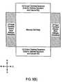
- FIG. 9 ( b )is a plan view of a substrate showing another layout of circuitry in the substrate.
- FIG. 9 ( c )is a plan view of a substrate showing one layout of circuitry in a substrate used for the present invention.
- FIG. 9 ( d )is a plan view of circuitry for an embodiment of the present invention using a plurality of subarrays.
- FIG. 10 ( a )is an electrical schematic of peripheral circuitry coupled to an array.
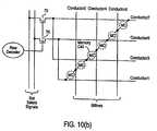
- FIG. 10 ( b )is another electrical schematic of peripheral circuitry coupled to an array.
- FIG. 11is an electrical schematic of peripheral circuitry coupled to an array used in one preferred embodiment of the present invention.
- FIG. 12is a cross-sectional elevation view of an array showing a contact between three levels of the memory array.
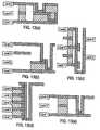
- FIG. 13 ( a )illustrates a contact between levels 1 and 3 .
- FIG. 13 ( b )illustrates a contact connecting levels 1 , 2 and 4 .
- FIG. 13 ( c )illustrates a contact between levels 1 , 3 and 5 .
- FIG. 13 ( d )illustrates a contact between levels 1 through 5 .
- FIG. 13 ( e )illustrates a contact between levels 1 and 3 .
- a field programmable nonvolatile memory cell and memory arrayis disclosed.
- numerous specific detailsare set forth in order to provide a thorough understanding of the present invention. However, it will be apparent to one skilled in the art that the present invention may be practiced without these specific details. In other instances, well-known circuits and processes have not been described in detail in order not to obscure the present invention.
- the field programmable nonvolatile memory cell of the present inventionis built above, rather than in, a planar substrate. Therefore, this memory cell can be stacked vertically in numerous layers to form a three dimensional array. Each layer of memory cells interacts only with the layer above and the layer below, which makes vertical stacking of layers quite simple.
- FIG. 4 ( a )shows one embodiment of our newly invented memory cell. It has two explicit terminals: an input terminal 20 and an output terminal 21 . Between these terminals, the memory cell contains a steering element 22 and a state change element 23 connected in series. Neither the input terminal 20 , nor the output terminal 21 , nor the steering element 22 , nor the state change element 23 is built in the planar semiconductor substrate.
- the steering element 22is a device with a strongly asymmetric current-versus-voltage characteristic; it conducts more readily in one direction than in the other.
- the purpose of the steering element 22is to ensure that current flow through the memory cell is substantially unidirectional. This unidirectional behavior enables the memory decoders to establish a unique circuit path to each individual memory cell, allowing it to be individually accessed (for reads and for writes) regardless of the state of all other cells.
- the state change element 23is a device which can be placed in more than one state, and whose state is not lost or altered when electrical power is removed.
- One possible implementation among the many discussed below,is a dielectric-rupture antifuse, having the states ⁇ high impedance ⁇ and ⁇ low impedance ⁇ . These two stored states accomplish the encoding of one bit of memory.
- the steering element 22 and the state change element 23are stacked vertically in a “pillar” shaped arrangement having a generally rectangular cross-section.
- the pillaris vertical and so is the current flow.
- currentcan flow either upwards or downwards. In fact, in one embodiment, current flows upwards in some layers of a vertical stack of cells, and downwards in the other layers.
- the state change element 23is chosen so that it can be switched from its initial state to another state by electrical means, thereby making the memory field programmable.
- the state of a dielectric-rupture antifusemay be changed electrically by applying a relatively large voltage (when compared to the voltage used for reading) across the input and output terminals of the memory cell.
- the memory cell of the present inventionis capable of being fabricated with full self-alignment in both the X (east-west) and Y (north-south) directions.
- This means the pillarsare defined by, and are automatically formed by, the intersection of an input conductor and an output conductor.
- the cellcan be made quite small, since its feature sizes need not include often used allowance for misalignment tolerances.
- the number of photolithographic masking steps needed to build the cell of FIG. 4 ( a )is small.
- three masking stepsare needed: one to pattern the bottom conductor and cell material, another to pattern the upper conductor and cell material, and a third to provide contact holes outside the array for vertical electrical connections.
- This pattering schemeresults in a self alignment of the cell pillar (i.e., the steering element and the state change element) to the upper and lower conductors.
- a second level of cellsis added vertically above the first level, only two additional photolithographic steps are needed: one for the next level conductor and the cell material, and the second for the contacts outside the array.
- the top conductor of the lower level of cellsforms the bottom conductor of the top layer of cells.
- the arraycontains (N) levels of cells, there are (N+1) conductor layers and (N+1) photomasking steps in the fabrication of the cell array itself. There are also a number of additional photomasking steps to form contacts. These contacts are outside the cell array; they make connection between the array conductor layers and the peripheral circuits.
- the memory cellmay also be fabricated using alternative embodiments; the self-aligned pillar formation described above may be replaced by a formation involving the use of a pillar formation photomask. This would eliminate the self-alignment of the pillar to the conductors, but would be advantageous in fabrication processes that could potentially exploit the physics of free sidewalls. These processes include steering element formation using solid-phase crystallization of amorphous silicon, laser crystallization of amorphous or polycrystalline silicon, and other processes apparent to persons skilled in the art.
- the contact to the upper conductor layer in both the self-aligned fabrication process and the non-self-aligned fabrication process described aboveis exposed by the planarization of the insulation, requiring no photomask step. This process may be replaced by a contact formation photomasking step, as would be apparent to persons skilled in the art.
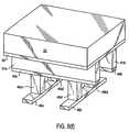
- a substrate beneath the memory cell arrayis available for use other than for defining the memory cells.
- this areamay be used to good advantage by laying out substantial portions of the row decoders, column decoders, I/O multiplexers, and read/write circuits directly beneath the memory cell array.
- Array ⁇ ⁇ Efficiency( total ⁇ ⁇ area ⁇ ⁇ devoted ⁇ ⁇ to ⁇ ⁇ memcells ) ( total ⁇ ⁇ area ⁇ ⁇ devoted ⁇ ⁇ to ⁇ ⁇ memcells ) + ( total ⁇ ⁇ area ⁇ ⁇ devoted ⁇ ⁇ to ⁇ ⁇ non ⁇ ⁇ memcells )
- an input terminal 20also called a wordline
- an output terminal 21also called a bitline
- the cellmay also contain “implicit” or “widely shared” terminals which are unavoidable consequences of its construction, and which are common to large groups of cells at once.
- an implicit terminalis the semiconductor substrate, which forms a parasitic capacitance to each memory cell. To simplify the figures and the discussion, these implicit terminals are omitted, but as will be appreciated these implicit terminals might affect the functionality and performance of the memory cell.
- the invented memory cellis referred to as a “two terminal structure”, meaning there are two explicit, local, terminals, possibly with additional terminals which are implicit rather than explicit.
- the memory cellBetween its input terminal and output terminal, the memory cell consists of a series connection of a steering element and a state change element.
- the steering elementmay be connected to the input terminal (and the state change element connected to the output terminal), and in other embodiments they may be reversed: the state change element may be connected to the input terminal and the steering element connected to the output terminal.
- the steering elementis a semiconductor element that has a strongly asymmetric current-versus-voltage characteristic; it conducts much more readily in one direction than in the other.
- Some possible implementations of the steering elementare (i) a PN junction diode, in amorphous, microcrystalline, polycrystalline or single crystal semiconductor (e.g., Si, Ge, SiGe, GaAs, InP, etc.); (ii) a metal-semiconductor Schottky diode; (iii) a junction field-effect transistor with gate connected to source (or to drain); (iv) a MOSFET with gate either floating, or connected to source or connected to drain; (v) a Zener diode, avalanche diode, or tunnel diode; (vi) a four-layer diode (SCR); (vii) a P-I-N diode in amorphous, microcrystalline, polycrystalline or single crystal semiconductor; and others that will be readily apparent to those skilled in the art.
- anodeFor descriptive purposes in this disclosure the two ends of the steering element are referred to as “anode” and “cathode”, arranged so that conventional current flows more readily from “anode” to “cathode” than from “cathode” to “anode”.
- These labelsare consistent with standard terminology for a PN junction diode: conventional current in a PN junction diode flows from anode to cathode.
- the present inventionis not limited to the use of a PN junction diode for its steering element (as was discussed in the preceding paragraph); the adoption of the same terminal labeling as a diode is merely for convenience and familiarity.
- the steering elementis “forward biased.” But when the cathode voltage exceeds the anode voltage, we will say the steering element is “reverse biased.”
- the steering elementcan be oriented two different ways: (1) with its anode facing the input terminal and its cathode facing the output terminal; (2) with its cathode facing the input terminal and its anode facing the output terminal. Either orientation can be made to function correctly, by appropriate design of the memory decoders and read/write circuits, and neither orientation is strongly preferred over the other.
- the state change elementis where data is actually stored in the memory cell. It is a device that can be placed in more than one state, and is so chosen that its state is not lost or altered when electrical power is removed.
- Some examples of the types of states that may be employed in a state change element according to the present inventionare (i) (high impedance state) and (low impedance state); (ii) (state with peak capacitance at voltage V1) and (state with peak capacitance at voltage V2); (iii) (state with Hall effect voltage positive) and (state with Hall effect voltage negative); (iv) (state with polarization vector pointing up) and (state with polarization vector pointing down) and others.
- the state change elementinclude, but are not limited to, (a) dielectric-rupture antifuses; (b) intrinsic or lightly-doped polycrystalline semiconductor antifuses; (c) amorphous semiconductor antifuses; (d) metal filament electromigration fuses, either of the reversible (U.S. Pat. No. 3,717,852) or irreversible type; (e) polysilicon resistor-fuses, either of the reversible (U.S. Pat. No. 4,420,766) or irreversible type; (f) ferroelectric capacitors; (g) capacitors with trap-induced hysteresis; (h) coulomb blockade devices; and others.
- the state change element of the memory cellis fabricated and placed in a certain one of its possible states; this is called the “initial state.”
- the initial stateFor example, if the state change element is a dielectric-rupture antifuse having the two states (ruptured dielectric) and (intact dielectric), the initial state of this element is (intact) after manufacturing and before programming.
- Other embodiments of state change elementswill have different sets of states and thus different initial states.
- this initial statethe “logic zero” state denotes the initial value stored in the memory cell during semiconductor manufacturing. But of course other conventions, calling the initial state e.g. “logic one,” would be equally valid, and the choice is merely a matter of preference or convenience rather than technological necessity.
- the memory cellis programmed by causing the state change element to transition from its initial state into a new state.
- Many embodiments of the state change elementcan be caused to change state by applying a suitably large voltage across the memory cell, from input terminal to output terminal.
- the state change elementis embodied as a dielectric-rupture antifuse, it is programmed by applying a large voltage across the cell's terminals (or by forcing a large current through the cell), with the polarity chosen such that the steering element is forward biased. This places a large electric field directly across the dielectric antifuse, which ruptures the dielectric, thus changing the state of the state change element.
- One possible method for programming a dielectric-rupture state change elementis to ground the memory cell's output terminal and simultaneously raise its input terminal to a large positive voltage (assuming the steering element is so oriented that its anode faces the input terminal and its cathode faces the output terminal, i.e., steering element is forward biased when the input terminal is at a higher voltage than the output terminal). If the steering element is oriented the other way, with anode facing the output terminal and cathode facing the input terminal, the designer can simply reverse the programming voltages and keep the steering element forward biased during programming: ground the input terminal and simultaneously raise the output terminal to a large positive voltage. Many other voltage arrangements for forward biasing the steering element and programming a dielectric-rupture state change element will be readily apparent to those skilled in the art.
- state change elementcan be caused to change state by forcing a suitably large current through the memory cell, rather than forcing a large voltage across the memory cell.
- the state change elementis embodied as a polysilicon-resistor fuse, it may be programmed by connecting a current source to its input terminal and simultaneously grounding its output terminal (assuming this polarity forward biases the steering element). Assuming the current is large enough, it alters the resistance of the polysilicon-resistor fuse, thus changing the state of the state change element and programming the cell.
- nonselected memory cellsDuring programming, it is possible for nonselected memory cells to be reverse-biased by the full programming voltage. Accidental writes of nonselected memory cells might occur, if the reverse leakage current of the steering element exceeded the programming current necessary to change the state of the state change element.
- the characteristics of the steering and state change elementsshould be matched to one another; a state change element that requires a large current to program (e.g., an instrinsic poly fuse) can be used with a rather high-leakage steering element, while a state change element that programs at very low current (e.g., a dielectric rupture antifuse) requires a low-leakage steering element.
- the invented memory cellcan be embodied either as a one-time programmable nonvolatile memory, or as a write/erase/rewrite nonvolatile memory, depending on the state change element selected.
- a thin, highly resistive, polycrystalline silicon film antifuseis employed as the state change element (as taught in U.S. Pat. No. 4,146,902)
- its programming operationis irreversible and the cell is one-time programmable.
- all cellscontain “logic zero”.
- Those cells whose desired contents are “logic one”are programmed, irreversibly, by forcing the state change element into a new state.
- Logic zeroesmay become logic ones (by programming), but logic ones may NOT become logic zeroes (since programming is irreversible in this type of state change element).
- a metal-via-insulator-silicon filament fuseis employed as the state change element (as taught in U.S. Pat. No. 3,717,852)
- its programming operationis reversible and the cell may be written, erased, and rewritten. After manufacturing and before programming, all cells contain “logic zero”. Those cells whose desired contents are “logic one” are programmed. However, for this state change element, programming is reversible and logic values may be changed from zero to one and back from one to zero, if desired.
- a state change element having a write/erase/rewrite capabilitymay be employed, whose programming operation is electrical but whose erase operation is not necessarily electrical.
- the erase operationmay be selectively applied to a single memory cell, or it may be applied to all memory cells at once, “in bulk,” such as by exposing them to a strong source of ultraviolet light as is done with UVEPROM memories.
- a bulk erase operationmay be initiated by heating the integrated circuit, either from a heat source external to the IC or from a heater directly on the IC.
- a bulk erasemight be initiated by placing the state change elements in a strong magnetic field.
- a floating gate MOS deviceallows numerous possible implementations of multi-level storage, providing more than 2 states for a state change element, as is well known in the art.
- the field programmable nonvolatile memory cellconsists of a vertical pillar, with a conductor at the bottom of the pillar and another conductor at the top.
- the bottom conductoris a relatively long conductor line or wire on a first conductor layer. This conductor runs in a certain direction (for example, east-to-west).
- the top conductoris a relatively long conductor line or wire on a second conductor layer, vertically above the layer that forms the bottom conductors.
- the top conductorsrun in another direction (for example, north-to-south).
- the angle between the top and bottom conductorsis preferably ninety degrees (i.e. it is preferred they are orthogonal) but this is not mandatory.
- the memory cell pillaris located at the intersection where the top conductor crosses over a projection of the bottom conductor.
- the conductors on each levelare parallel spaced apart conductors where for instance, the space between each conductor is equal to the conductor's width.
- the first conductor layer(“conductors 1 ”) contains a large number of parallel conductors all running in the same direction, for example, east-to-west.
- the second conductor layer(“conductors 2 ”) also contains a large number of parallel conductors all running in the same direction, for example, north-to-south, preferably perpendicular to the conductor direction of the first conductor layer as shown in FIG. 5 .
- a conductor on conductors 2crosses over (or “intersects”) a conductor on conductors 1 , one of our field programmable nonvolatile memory cells is fabricated. This is shown in FIG. 4 ( b ).
- the invented memory cellcontains a conductor, then a pillar, then another conductor: conductors 1 ⁇ pillar ⁇ conductors 2 .
- Conductors 1is on the bottom and conductors 2 is on the top.
- conductors 2is the bottom of a new level of memory cells, vertically stacked above the first level: conductors 1 ⁇ pillar 1 ⁇ conductors 2 ⁇ pillar 2 ⁇ conductors 3 .
- the present inventionstacks multiple levels of memory cells above one another: a vertical stack having (N) levels of memory cells contains (N) levels of pillars and (N+1) layers of conductors.
- a vertical stack of (N) pillarsuses 1/N as much surface area as an assembly of (N) pillars that are not stacked vertically; vertical stacking gives an N-fold improvement in density.
- a memory pillar's bottom conductoris the top conductor of the memory pillar below, and a memory pillar's top conductor is the bottom conductor of the memory pillar above. This makes stacking especially simple and flexible.
- the two conductors at either end of a memory pillarare perpendicular. And since conductors are shared between levels of pillars, the result in this embodiment is that even-numbered conductors run in one direction, and odd-numbered conductors run in the perpendicular direction. For example, suppose conductors 1 runs east-to-west. Conductors 2 would be perpendicular to conductors 1 , so conductors 2 would run north-to-south. Conductors 3 would be perpendicular to conductors 2 , so conductors 3 would run east-to-west. Conductors 4 would run north-to-south (perpendicular to conductors 3 ), and so forth. Thus conductors 1 , 3 , 5 , . . . run east-to-west, and conductors 2 , 4 , 6 , . . . run north-to-south (in this example).
- a conductor layer(say, conductor layer number J) runs north-to-south, and adjacent conductor layers (numbers J ⁇ 1 and J+1) run east-to-west.
- a conductor's vertical projection on layer (J) crosses over a conductor on layer (J ⁇ 1)a memory cell pillar is created.
- a conductor's projection on layer (J+1) crosses a conductor on layer (J)a memory cell pillar is created.
- Memory cell pillarsare defined and patterned by the intersection (crossover) of the conductors, and so the pillars are selfaligned to the conductors.
- Self-alignmentis an extremely important advantage, because it lets the photolithographic patterns of the memory cell be designed without including any extra allowance for misalignment tolerances.
- the pattern features of our selfaligned memory cellmay be made smaller, resulting in a smaller cell area, which gives higher density and lower cost.
- the steering elementconsists of a polycrystalline silicon PN junction diode
- the state change elementconsists of a poly-oxide-poly dielectric rupture antifuse.
- Other embodimentsare set forth in the body of this application.
- a pillarcontains four layers of material in a layer stack, deposited sequentially as shown in FIG. 6 ( a ): (1) a layer of P+ doped polysilicon 40 ; (2) a layer of N-doped polysilicon 41 ; (3) a layer of silicon dioxide 42 ; (4) a layer of N+ doped polysilicon 43 .
- Layers (40) and (41)form a PN junction diode (the steering element), and layers ( 41 - 43 ) form a poly-oxide-poly dielectric rupture antifuse.
- the stack of four materials which together create the memory cellsare referred to as the “layer stack” 45 .
- FIG. 6 ( a )An alternate stack is shown in FIG. 6 ( a ) as stack 450 . Again it includes conductors at the ends of the stack, specifically 460 and 480 which may be fabricated from any conductive material such as a metal or a polysilicon.
- the steering element in stack 450comprises a first layer 400 of P+ doped semiconductor such as microcrystalline silicon, and a second layer 410 of N doped semiconductor such as microcrystalline silicon.
- the state change elementcomprises the layer 420 .
- Layer 420may be an amorphous silicon layer used to form an antifuse. This layer has a nominal high resistance, however, after a large current is passed through it for programming, its resistance will be substantially lower.
- the layer 430is shown as an N+ layer to provide good electrical contact to the overlying conductor 480 . Layer 430 could be amorphous, microcrystalline or polysilicon but the processing methods need to be low temperature to maintain the amorphous structure in layer 420 .
- FIG. 6 ( a )Another stack 405 is also shown in FIG. 6 ( a ). It comprises an N-polysilicon layer 400 , a silicon dioxide layer 402 and an N+ polysilicon layer 403 . Again, the layers 400 or 403 could be microcrystalline or amorphous semiconductor layers.
- the stack 405is sandwiched between the conductors 406 and 408 .
- the steering elementis a Schottky diode formed by the metal of conductor 406 and the layer 400 .
- the state change elementis an antifuse formed by layer 402 .
- layers 406 and 408may be titanium silicide or aluminum with a thickness of approximately 1000A.
- the layers 400 , 402 and 403may be 500A, 80A, and 500A in thickness, respectively.
- the fabrication sequence for the memory cellis schematically illustrated in FIGS. 6 ( b )- 6 ( g ).
- the layer stack 45(or the stacks 450 and 405 ) is a continuous sheet that extends across the entire integrated circuit (indeed across the entire wafer) such as shown in FIG. 6 ( b ).
- the self-alignment methodis a two-etch-step procedure: In the first etch step, this layer stack (a continuous sheet) is patterned into long straight strips running (say) east-to-west, by etching them with the same patterning step that etches the east-to-west conductors on the conductor layer below.
- a second conductor and layer stackis deposited.
- This stackis patterned into long straight strips running north south. Etching used to pattern the north-to-south lines continues until the first layer stack has also been etched through the steering element. This results in pillars formed on the east-to-west running lines. The resulting pillars are perfectly aligned to both the conductor below and the conductor above since both the pillars and the conductors are etched simultaneously.
- the semiconductor layers within the layer stackmay be deposited as microcrystalline or polycrystalline, and then laser treated to improve crystallinity and enhance the dopant activation.
- the cross-section of the pillarwill be rectangular with one dimension being equal to the width of the bottom conductors and the other dimension equal to the width of the top conductors. If these conductors have equal width then the cross-section will be square.
- the patterning in both east-to-west and north-to-southuses well-known photolithographic steps widely used in the semiconductor industry and may use either wet or dry etching. Also, the silicon used in the cells and when used for the conductors may be doped insitu or after being deposited, for example, by ion implantation.
- etchingFor example “liftoff” technology or “Damascene” technology or an additive rather than subtractive patterning technology may be employed instead of etching.
- layer stackshould be patterned in two separate steps, once with the mask that defines the conductors below, and again with the mask that defines the conductors above. This holds true regardless of the specific fabrication techniques used to pattern the various layers.
- each conductor layeris selfaligned to both the layer stack below, and the layer stack above. Therefore the etching steps which selfalign the conductors to the pillars, must etch away material from three different layers: the layer stack above, the conductor layer, and the layer stack below.
- the processingmay begin with a wafer that may have received prior processing steps, for example, CMOS transistors may be fabricated in the monocrystalline substrate for the peripheral circuitry.
- An insulatorthen is deposited, and preferably, planarized (using chemical-mechanical polishing (“CMP”), resist etchback planarization, or any of a number of other technologies for planarization).
- CMPchemical-mechanical polishing
- the first conductor layeris deposited such as layer 46 of FIG. 6 ( b ), and then the first layer stack 45 is deposited.
- FIG. 6 ( b )shows the wafer at this stage.
- FIG. 6 ( c )shows the wafer at this stage.
- the pillar layer stack and bottom layerhave, been etched into long continuous strips ( 46 a and 45 a ) and ( 46 b and 45 b ), not isolated individual pillars.
- the edges of the pillar layer stack 45 a and 45 bare aligned to the edges of the conductor 46 a and 46 b layer, since both were etched at the same time with the same mask.
- the conductorsgenerally comprise coplanar conductors, such as aluminum or other metals, silicides, or doped silicon conductors, for each level.
- the dielectricfills the voids between the strips (and pillars) and thus adds support to the array. Also it should be noted that the planarization must reveal the upper surface of the strips so that the conductor layer that follows contacts the strips. The planarized dielectric also forms the layers through which the vias and vertical conductors of FIG. 13 pass.
- FIG. 6 ( d )shows the wafer at this stage. Note that the planarization automatically gives a selfaligned contact between a pillar layer stack (such as 45 b ) and the subsequent conductor layer (such as 50 ) above it.
- the conductors 2 maskis applied, and its features are etched downward into three distinct strata: pillarstack 2 ( 51 ), conductors 2 layer 50 , and pillarstack 1 ( 45 a and 45 b ). (This etch stops below the steering element within 45 a and 45 b , providing a unique circuit path through the memory cell).
- An insulatoris deposited on the wafer and planarized (using CMP or other means).
- FIG. 6 ( e )shows the wafer at this stage. Note that the conductors 2 mask+etch has completed the definition of the individual pillars ( 45 a 1 , 45 a 2 , 45 b 1 and 45 b 2 ) in the layerstack 1 .
- these pillars in the layerstackl layerare aligned to both the conductors 1 layer ( 46 a , 46 b ) and to the conductors 2 layer ( 50 a , 50 b ), thereby achieving the goal of self-alignment.
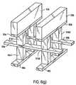
- FIG. 6 ( f )shows the wafer at this stage.
- the conductors 3 maskis applied, and its features are etched downwards into layers stack 3 , conductors 3 , and stack 2 . (This etch stops below the steering element of layer stack 2 and is intended to leave the conductor 2 layer intact.)
- An insulatoris deposited on the wafer and planarized (using CMP or other means).
- FIG. 6 ( g )shows the wafer at this stage.
- the conductors 3 mask+etchhas completed the definition of the individual pillars in the layerstack 2 layer (such as 51 a 1 , 51 a 2 , 51 b 2 ).
- the pillarsare vertically stacked directly above one another as illustrated in FIG. 6 .
- pillarsare lined up in vertically aligned stacks.
- this vertical stacking of pillars directly above one anotheris not a requirement.
- Memory cell pillarsare automatically formed wherever a conductor on conductor layer (J+1) crosses over a conductor on conductor layer (J). This is true even if the conductor layers are not lined up directly above one another, giving vertical stacks of pillars. In fact it may be preferred that the pillars not be stacked vertically; that is they are offset from one another, as illustrated in FIG. 7 . Compare FIG. 5 (vertical stacks of pillars) to FIG. 7 (pillars offset from one another) to see the effect. Offset or staggered pillar placement such as shown in FIG. 7 , may be advantageous in practice. It may help give a smoother wafer surface, more suited to planarization and polishing.
- electrode or conductor materialis etched along with device material. Since most plasma metal etches also etch polysilicon, a practical combination of materials that enables such dual etching would be aluminum and polysilicon, for example. Control of the etching process may be effected, if desired, through the use of etch chemistries that are selective (e.g., preferentially etching polysilicon, but stopping on aluminum), or through the use of barrier materials that are not etched by the etchants that remove electrode and device material.
- the state change elementmay also be used as an etch stop, particularly if it is an oxide rupture type.
- Refractory metalssuch as molybdenum and tungsten are compatible with conventional CVD deposition temperatures for Si and may be used for the conductors.
- Metal suicidesare compatible with even higher temperatures used to activate dopants in Si. Even heavily doped Si itself can be used as a conductor. The choice may be dictated based on resistivity and integration concerns including etch characteristics.
- planarization described after the first half-step of the foregoingis necessary to form self-aligned contacts to the half-etched cells (i.e., the lines running in the east-west direction in the foregoing example).
- Such planarizationmay be effected through a variety of means well known in the art, such as chemical-mechanical polishing (CMP), etched-back spin-on dielectric layers, and etched-back spin-on polymers, to cite three well-known examples.
- CMPchemical-mechanical polishing
- etched-back spin-on dielectric layersetched-back spin-on polymers
- a second planarizationmay be performed after deposition of an electrode layer to insure a planar electrode surface for subsequent deposition of device material layers.
- the foregoing process sequenceexploits self-alignment to reduce the required alignment tolerances between the pillar and the conductors.
- This embodimentmay be substituted with an embodiment involving one or more additional photomasking steps to explicitly define the pillar itself, rather than defining it using the intersection of two conductor photomasking steps, as is done in the self-aligned process.
- Thismay be advantageous in various processes that could exploit the explicitly defined sidewalls that would result from such a process.
- solid-phase crystallization of amorphous siliconcould be used to form the steering element layer stack. The free energies of the sidewalls would be expected to favor the formation of a single crystal or grain within the steering element, which may be advantageous in some system embodiments.
- a photomasking stepwould be used to define a bottom conductor. This would be etched. Then, the layer stack required to form the state change and steering elements would be deposited. Another photomasking step would be used to define the pillar, which would be etched. After this etch, an insulating material would be deposited and planarized as in the self-aligned cell, exposing the top of the pillar to form a self-aligned contact. The top conductor would then be deposited and the process would be repeated for subsequent levels of cells as required.
- the pillarcould be formed prior to patterning the bottom conductor.
- the entire layer stack for the bottom conductor, the steering element, and the state change elementwould be deposited.
- the pillarwould then be lithographically defined and etched down through the steering element.
- the bottom conductorwould then be defined and etched.
- This structurewould be passivated using a planarized insulator contacting scheme, as described above.
- the self-aligned contactcould also be replaced by an explicit contact forming photomasking step.
- the various device fabrication stepsmay result in the presence of residual chemicals or dangling bonds that may degrade device characteristics.
- device leakagecan result from the presence of such dangling bonds or chemicals (e.g., incompletely removed photoresist).
- a low-temperature (e.g., ⁇ 400C) plasma oxidation exposuremay be used to grow a clean-up oxide on the edges of the device pillar, thereby passivating edge traps.
- the growth of the oxideis self-limiting because the oxygen species diffuse only slowly through previously grown oxide, resulting in extremely uniform oxide thickness and, therefore, improved manufacturability.
- Pullasma oxidationmay also be used to form an anti-fuse layer.
- Oxide depositionmay also be used to passivate the surface, for example, either alone or in conjunction with a grown oxide.
- device materiale.g., polysilicon
- electrode materiale.g., metals
- in-situ doped polysiliconmay be deposited at low temperatures using LPCVD (low pressure chemical vapor deposition), PECVD (plasma-enhanced chemical vapor deposition), PVD (physical vapor deposition), or UHVCVD (ultra high vacuum chemical vapor deposition).
- LPCVDlow pressure chemical vapor deposition
- PECVDplasma-enhanced chemical vapor deposition
- PVDphysical vapor deposition
- UHVCVDultra high vacuum chemical vapor deposition
- Electrode materiale.g., metal
- Low temperature processinghelps to reduce the severity of this problem, but may be insufficient to solve it completely.
- barrier materialsmay be employed. Examples include titanium nitride (TiN), tantalum (Ta) or tantalum nitride (TaN), among many that are well known to the art.
- a thin dielectric layeris employed as an antifuse element.
- good uniformity of dielectric thickness, as well as a low film defect density (e.g., of pinholes in the dielectric)are among highly desirable properties.
- the quality of the dielectricmay be enhanced through a variety of means, such as rotating (continuously or periodically) the substrate and/or source during deposition; forming the dielectric by thermal means using plasmas or low-temperature growth chemistries; or by employing liquid-phase dielectric deposition means.
- One method for reducing the number of masking stepsis to employ vias that interconnect several electrode layers.
- the viasmay be rectangular, rather than square, to allow a relaxation in alignment tolerances.
- the x-edge via sizemay be made substantially looser than the pitch of the x-lines in the y-direction, resulting in a rectangular via. Vias are discussed in conjunction with FIGS. 12 and 13 .
- theycan be progressively shorter, or longer, or longer in some layers and shorter in others, to allow area on the periphery of the array for contacts.
- These contactscan reach down to lower levels, for instance, every other lower level without interfering with conductors in the intermediate layer.
- Contactsare required outside the array to connect the conductors in the array to the drive circuitry.
- Transistors built into the substratewill typically provide drive.
- Drive transistorscould also be built above the substrate using materials common to the array.
- the simplest implementation of contactsis to have a via mask for each level of the array. These contacts are used to connect an upper level through all the levels below it to electrically connect to the substrate. These contacts are built either stacked directly over one another or staggered, both methods being common in the semiconductor industry.
- the vias and contactsare used to provide conductive paths between the conductors in the array and the periphery circuitry.
- contactsare formed in the periphery of the array to contact the decoders, column I/O circuitry and row address decoders shown in FIGS. 9 ( a ), 9 ( b ) and 9 ( c ).
- the upper most layermay be used for power distribution.
- One straight-forward plan for making contact, with each of the levelsis to use one masking and etching step per level, which step occurs before the formation of the layer used to define the conductors. This masking step forms openings to the layer beneath and provides contacts as needed.
- FIG. 12An example of this is shown in FIG. 12 .
- a contact 110is masked and etched through the substrate isolation 100 to the substrate contact 101 prior to beginning the fabrication of the array.
- Conductor layer 106is deposited prior to the memory stack 131 .
- the lower level of the memory stack 107is a heavily doped semiconductor in this example. This is important in this example because the heavily doped semiconductor will provide an ohmic connection and therefore does not need to be completely removed from the conductor layer.
- Region 120 and the area over contact 110are formed during the formation of the strips that make up level 1 .
- 120is electrically isolated from the other conductors on level 1 by virtue of the level 1 mask layout.
- Dielectricis then deposited and planarized to expose the top surface of level 1 .
- Contact opening 111is then formed through the layers of level 1 at least down to the heavily doped layer 107 .
- Level 2 conductor 122 and memory stack layersare then deposited and patterned in the same way as level one was patterned. Again, the mask is used to isolate this region from the conductors of the level 2 array. Dielectric is again deposited and etched back to expose the top surface of level 2 . Just as in level 1 , a contact mask is used to form opening 112 through the memory cell elements down to the heavily doped material.
- level 3 conductoris deposited into the opening 112 to form a continuous electrical connection from level 3 to the substrate.
- contacts from any levelmay be made to a region in the substrate with one additional masking step per layer.
- less than one masking step per layeris used to form the conductive paths to the substrate. This is possible in cases where more than one conductor contacts a single substrate region. Note in FIG. 13 ( c ), for instance, that conductors 1 , 3 , and 5 are connected to the same substrate regions.
- FIGS. 13 ( a )- 13 ( e )Several possible structures for contacts are shown in FIGS. 13 ( a )- 13 ( e ).
- FIG. 13 ( a )an arrangement is shown where contact is made between conductors in level 1 (or level N) and level 3 (or level N+2). Note that in this arrangement, the conductors in level N+1 are made shorter than the conductors in level N and level N+2, to allow ample space for the contact to be made without interfering with conductors in level N+1.
- the contactsince it is between adjacent levels, extends through the memory stack shown in the crosshatching.
- FIG. 13 ( b )a contact is shown from a conductor in level 4 (or level N+3) which contacts conductors in levels 1 and 2 (or levels N and N+1). Note in this arrangement that the conductor in level N+2 is shorter than the conductor in level N, allowing the structure fabricated from level N+3 to reach down and contact two underlying conductors. Only a single opening needs to be defined in the insulator to form this contact and the opening is disposed through the oxide or other insulator used in the planarization step.
- FIG. 13 ( c )Another contact is shown in FIG. 13 ( c ) where conductors from levels 1 , 3 and 5 are connected to contact a substrate region. Here the conductors in levels 2 and 4 are staggered so as not to interfere with the contact. Again only a single masking step is used to define this contact.
- FIG. 13 ( d )a contact structure is shown where levels 1 , 2 , 3 , 4 and 5 each have a conductor connected to a common substrate region.
- FIG. 13 ( e )a contact from level 3 (or level N+2) to level 1 (or level N) is shown.
- FIG. 13 ( a )a single opening through insulation material is made.
- the resistivity of the vertical conductorsis important. Metals, silicides and insitu doped silicon can be used. Implanted silicon is not currently preferred because of the difficulty of doping the silicon on the sidewalls of the contact.
- an openingis first etched from an upper layer through several lower layers. After the insulation has been etched to expose the edges of the layers, the memory cell material is then etched isotropically to expose more of the conductor. In this way, an isotropic deposition of a material like polysilicon or CVD W can be used to obtain a large surface area on each conductor to insure low contact resistance.
- FIGS. 13 ( d ) and 13 ( c )are used to limit the number of mask steps needed in the process. Use of either one could reduce the mask count from 2N+1 to N+2.
- self-alignmentpermits the pattern features of the memory cell to be small, since it is not necessary to allow for misalignment tolerances when laying out the features. These smaller features allow reduction in the memory cell area, in fact smaller than it otherwise could be without self-alignment.
- each layer of the invented memory cell arrayare especially simple: they are merely a highly repetitive, regular set of closely spaced, long, straight parallel conductor lines. Their simplicity and regularity can be exploited in photolithography, allowing better resolution of smaller feature sizes than otherwise would be possible with arbitrary-shaped geometries. For example, if a (wafer stepper and illumination source and lens and photoresist) system were normally rated for X micron resolution (e.g. 0.18 microns), the simple and highly regular shapes of the present invention would permit lines and spaces substantially smaller than X microns.
- the present inventioncan take advantage of the fact that there are no arbitrary-shaped geometries; rather there is a highly repetitive, very simple pattern, which is well known in the field of optics and is called a “diffraction grating” in textbooks. It will be readily apparent to those skilled in the art, how to exploit the advantages of a diffraction grating pattern to achieve better resolution.
- FIG. 8 ( a )'s stack of six memory cell pillars ( 60 - 65 )is shown as a circuit schematic diagram in FIG. 8 ( b ). Notice that conductor layers 1 , 3 , 5 , 7 are spaced apart from one another in the schematic diagram, but in the physical structure ( FIG. 8 ( a )) they are vertically stacked directly above one another. Similarly, conductor layers 2 , 4 , 6 are vertically stacked in FIG. 8 ( a ) but spaced apart in FIG. 8 ( b ).
- FIG. 8 ( a )There are six memory cell pillars in FIG. 8 ( a ): one where conductors 2 crosses conductors 1 , one where conductors 3 crosses conductors 2 , . . . , and one where conductors 7 crosses conductors 6 . In the schematic of FIG. 8 ( b ) these are shown along a diagonal. At the bottom left, a memory cell (containing a steering element and a state change element) is shown between conductors 2 and conductors 1 . FIG. 8 ( b ) also shows a memory cell where conductors 3 crosses conductors 2 , another cell where conductors 4 crosses conductors 3 , etc.
- Adjacent layers of memory cell pillarsshare a conductor layer; thus they also share an I/O terminal.
- sharingonly occurs between terminals of like type: input terminals share a conductor layer with other input terminals, and output terminals share a conductor layer with other output terminals.
- This embodimentis advantageous, because it means each conductor layer is unambiguously either an input layer or an output layer. There is no mixing as would occur if a conductor layer was shared among input terminals and output terminals, so the peripheral circuitry is simplified. Input-terminal-driver circuits and output-terminal-receiver circuits need not be collocated and multiplexed onto the same conductor.
- a result of the like-terminals-shared preferenceis that the steering elements in the memory cells will be oriented alternately cathode-up, then cathode-down, then cathode-up, etc.
- conductor layer conductors 2is an output layer; then the cathodes of pillar 60 and pillar 61 both connect to conductors 2 .
- pillar 60must be oriented cathode-up and pillar 61 is cathode-down.
- conductors 2is an output layer
- conductors 3is an input layer.
- the anodes of pillar 61 and pillar 62connect to conductors 3 . So pillar 62 is cathode-up.
- the layers of pillarsmust alternate, cathode-up, cathode-down, up, down, up, and so forth (see FIG. 8 ( b )) for this embodiment.
- the layers shown in FIG. 6 ( a )will be in the order shown in alternate array levels and in the opposite order in the remaining levels. However, it should be recalled that it is not necessary to alternate the stack material for some embodiments.
- a further result of the preference for sharing like terminals of memory cellsis that it makes the conductor layers alternate between input terminals only and output terminals only. Since successive conductor layers run east-to-west, then north-to-south, then east-to-west, etc., this means that all input conductors will run the same direction (e.g. east-to-west), and all output conductors will run the same direction (e.g. north-to-south). So it will be especially easy to locate the input-terminal-driver circuits together (e.g. along the west edge of the memory array), and to locate the output-terminal-receiver circuits elsewhere (e.g. along the south edge of the memory array).
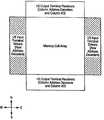
- the input-terminal-driver circuitry 67is located along the west edge of the array, and the output-terminal-receiver circuitry 68 is located along the south edge of the array, as shown in FIG. 9 ( a ).
- conventional memoriesput half the input-terminal-driver circuits along the east edge and half along the west edge; this is often done when the memory cell row pitch is very tight.
- conventional memoriessometimes place half the output-terminal-receiver circuits along the south edge and half along the north edge; this is done when the memory cell column pitch is very tight.
- FIG. 9 ( b )shows a conventional memory with this splitting performed.
- the input-terminal-driver circuitry in a nonvolatile memoryhas a shorter and less cumbersome name: “row address decoder” circuitry.
- the output-terminal-receiver circuitry in a nonvolatile memoryhas a shorter and less cumbersome name: “column address decoder and column I/O” circuitry. In this section of the disclosure, which discusses array organization outside the memory cell mats, this shorter name will be used.
- the field programmable nonvolatile memory of the present inventionincludes the organization of the memory chip into several smaller subarrays, rather than one single large array.
- Subarraysgive three important benefits: (1) they allow a simple block-level approach to redundancy; (2) they increase operating speed; (3) they lower operating power. Redundancy with subarrays can be quite straightforward. If the end product is to be a memory having (say) 8N bits, it is a simple matter to build nine subarrays on the die, each containing N bits. Then one of the nine subarrays can be defective, yet the die can still be configured and sold as a working 8N bit memory, by simply bypassing the defective subarray.
- Dividing the memory into subarraysalso increases speed; this is because the conductors are shorter (decreasing their resistance), and there are fewer memory cells attached to each conductor (decreasing the capacitance). Since delay is proportional to the product of resistance and capacitance, cutting conductor length in half cuts delay by a factor of four. Thus subarrays decrease delay, i.e. increase speed.
- Subarraysalso provide lower power operation. Since one important component of power is the capacitive charging and discharging of conductors in the memory array, decreasing the conductor capacitance will decrease power consumption. Cutting conductor length in half cuts capacitance in half, which cuts the capacitive charging and discharging current in half.
- the rows of a memory arrayare the inputs of the memory cells
- the columnsalso called “bitlines” are the outputs of the memory cells.
- a forcing functionis applied to the memory cell input (wordline), and for a read the result at the memory cell's output (bitline) is sensed, while for a write another forcing function is applied to the memory cell output (thereby forcing both terminals of the cell).
- the forcing functions used with the present inventionmay be voltage sources, current sources, waveshape generators (either high impedance or low impedance), charge packets, or other driving stimuli.
- FIG. 8 ( b )In order to unambiguously access each individual memory cell, for both reading and writing, a unique circuit path is established from the row lines, through the memory cell, to the column lines. A consequence of the uniqueness requirement is that all of the row lines cannot be driven simultaneously; this may be appreciated by considering FIG. 8 ( b ).
- the row lines (wordlines) in FIG. 8 ( b )are on conductor layers 1 , 3 , 5 , and 7 .
- the column lines (bitlines)are on conductor layers 2 , 4 , and 6 .
- FIG. 8represents a single vertical stack of memory cell pillars; it is the physical intersection of one single row and one single column.
- the drawing in FIG. 8 ( b )depicts the conductors spaced-apart for easier viewing, but in reality they are stacked above one another.
- a straightforward solutionis to only drive a single wordline, leaving all other wordlines undriven. This is diagrammed in FIG. 10 ( a ).
- a row decoder 70selects whether any of the wordlines along this row should be enabled.
- four layer-select signalsselect which conductor layer wordline should be enabled in the selected row. All but one of the layer-select signals are in the deselect condition (e.g. low voltage), and only one of the layer-select signals is in the select condition (e.g. high voltage). Thus only one wordline is driven, and the other three are not driven.
- FIG. 10 ( a )establishes a unique path to the array outputs.
- the wordline on conductors 5is selected, and suppose that sensing circuitry determines that conductors 4 is at a high voltage.
- FIG. 10 ( a )the arrangement in FIG. 10 ( a ) is costly; it includes a switching transistor for each of the wordline layers in the memory array. If there are a large number of vertical layers in the array (e.g. sixteen layers of memory pillars, requiring nine wordline conductor layers and eight bitline conductor layers), the switching transistors consume a lot of silicon area. This degrades die efficiency, which drives cost up and density down.
- the circuit in FIG. 10 ( b )only includes two switching transistors 75 and 76 , regardless of the number of vertical layers of memory cells in the array. There is one switching transistor for the first set of wordlines, and one switching transistor for the second set. Similarly there are two set-select signals, that determine which of the two wordline sets are driven. The greater the number of vertical layers of memory cells in the chip, the greater are the savings of FIG. 10 ( b ) compared to FIG. 10 ( a ).
- the first set-select signalis in the select condition (high voltage) and the second set-select signal is in the deselect condition.
- the wordlines on layers conductors 1 , conductors 5 , conductors 9 , . . . , etcare driven, while the wordlines on layers conductors 3 , conductors 7 , conductors 11 , . . . are not driven.
- There is only one (unique) path to the bitline on conductor 2this is the path from conductors 1 , through the memory cell between conductors 1 and conductor 2 , and onto the bitline on the conductor 2 layer.
- the other possible path, from conductors 3 , through the memory cell between conductors 3 and conductor 2 , and onto conductor 2is disabled because conductors 3 is in the second wordline set and is not driven.
- each selected columncould read or write (N) bits of memory simultaneously.
- One embodiment of the present inventiondoes indeed read (and/or write) N bits at once, in each selected column.
- Other embodimentsintroduce column multiplexor circuitry, which reduces the number of simultaneously accessed memory cells.
- FIG. 11shows another embodiment.
- Each bitlineis provided with its own switching transistor such as transistors 77 and 78 ; these transistors connect a bitline to a bidirectional I/O bus if this column is selected. During read operations, the bitline drives the I/O bus, but during write operations, the I/O bus drives the bitline. If there are (N) layers of bitlines, there are (N) switching transistors and (N) I/O bus conductors. The I/O bus conductor connects to peripheral circuits, including a sense amplifier (for reads) and a write driver (for writes).
- This column selection circuitryis far more costly than the row selection circuits shown in FIG. 10 ( b ). Since there must be a switching transistor for every bitline, if more and more layers of memory cells are stacked vertically, there will be more and more bitlines, hence more and more switching transistors.
- the column selection circuitrywill consume more silicon area than the row selection circuitry, especially when there are a large number of vertically stacked layers of memory cells. This is why it is preferred to fold the column select circuits under the memory array, more so than the row select circuits, as shown in FIG. 9 ( c ): the column circuits are a lot bigger. In fact, it would be a reasonable design decision to fold the column circuits underneath the memory array and completely forget even trying to fold the row select circuits beneath. The advantage comes from folding the column selects.
- a state change elementwhose different states correspond to different values of impedance.
- a dielectric rupture antifusehas two states: very low impedance and very high impedance, in which the impedances differ by several orders of magnitude.
- Embodiments such as thesecan use a “current-mode read” and a “voltage-mode or current-mode write,” as explained below.
- a current sourcecan be selected as the forcing function which drives the wordlines. If the memory cell is programmed (dielectric ruptured, thus low impedance), this driving current will pass through the memory cell and onto the bitline. The selected bitline will be switched onto the (bidirectional) I/O line, and the driving current will be passed onto the I/O line.
- a current-sensing amplifier connected to the I/O linedetects whether or not the driving current is passed onto the I/O line. If so, the cell being read contains a “logic one,” and if not, the cell contains a “logic zero.”
- the main advantage of a current-mode readis speed: by forcing and sensing current (rather than voltage), the need to charge and discharge the high-capacitance wordlines and bitlines in the memory array is avoided, so the wordlines and bitlines do not swing through large voltage excursions, which speeds up the read operation. Therefore current-mode reads are preferred in many embodiments of the present invention.
- a voltage sourcecan be selected as the forcing function which drives the wordlines.
- the bidirectional I/O buscan be driven with another voltage source.
- the I/O buswill be connected to the bitline (by the column select switching transistor) in the selected column, so the selected memory cell (at the intersection of the selected wordline and the selected bitline) will be driven by two voltage sources: one on the wordline, the other on the I/O bus. The large voltage difference between these two sources will be impressed directly across the selected memory cell, achieving a voltage-mode (large voltage excursion on the wordlines and bitlines) write.
- Voltage-mode writingcan, if necessary, provide very high current through the memory cell, which is advantageous with several embodiments of the state change element such as an amorphous-semiconductor antifuse.
- One possible benefit of limiting the maximum currentis to reduce the effect of IR voltage drops along the conductors of the array to ensure that a consistent programming energy is delivered to each memory cell, independent of the cell's location in the array.
- a consistent programming energycan be important because the characteristics of some state-change element materials may be sensitive to programming energy.
- the voltage necessary to program the state change elementmay exceed the voltage capabilities of the peripheral transistors. This is particularly true when the transistors are scaled for small dimensions (for example, channel length below 0.2 microns).
Landscapes
- Engineering & Computer Science (AREA)
- Computer Hardware Design (AREA)
- Manufacturing & Machinery (AREA)
- Semiconductor Memories (AREA)
Abstract
Description
- This application is a continuation of application Ser. No. 10/253,354, filed Sep. 23, 2002, which is a continuation of application Ser. No. 09/939,431, filed Aug. 24, 2001 (now U.S. Pat. No. 6,483,736), which is a continuation of application Ser. No. 09/714,440, filed Nov. 15, 2000 (now U.S. Pat. No. 6,351,406), which is a continuation of application Ser. No. 09/469,658, filed Dec. 22, 1999 (now U.S. Pat. No. 6,185,122), which is a divisional of application Ser. No. 09/192,883, filed Nov. 16, 1998 (now U.S. Pat. No. 6,034,882), each of which is hereby incorporated by reference in its entirety.
- 1. Field of the Invention
- This invention relates to low cost, high density semiconductor memories and, in particular, to semiconductor memories whose contents are “nonvolatile”: data stored in the memory is not lost or altered when electrical power is removed.
- 2. Background of the Invention
- There is an ever-increasing demand for ever-denser semiconductor memories, and customers continue to purchase these memories in ever-greater quantities, even as the number of bits per chip quadruples (approximately) every three years. Increasingly higher densities are required, at ever lower costs, to meet the needs of the marketplace.
- Semiconductor nonvolatile memories may be divided into two categories: (1) those in which data is permanently written during the manufacturing process and whose contents cannot be subsequently changed, called “mask ROMs” or “factory programmed ROMs”; (2) those in which data may be supplied after the finished memory device leaves the factory. This latter category is called “field programmable memories” because their contents may be written, by the user, when the semiconductor memory chip is deployed to its final application, “in the field”.
- Field programmable memories are further subdivided into “write once” memories and “write/erase/rewrite” memories. Those written once are referred to as “PROM” (programmable read only memories) or “OTP ROM” (one time programmable read only memories). And those memories that provide write/erase/rewrite capabilities have been referred to as “UVEPROM” (ultraviolet erasable programmable read only memories) or “EEPROM” (electrically erasable programmable read only memories) or “Flash EEPROM” (fast and flexible EEPROMs). In contrast, the contents of mask ROMs are permanently stored during manufacture, therefore mask ROMs are not erasable and are effectively “write only once, at the factory” memories.
- Field programmable memories are much more flexible than mask ROMs, since they allow system product makers to inventory a single general part-type for many applications, and to personalize (program the memory contents of) this one part-type in numerous different ways, much later in the system product flow. This flexibility lets system manufacturers more easily adapt to fluctuations in demand among different system products, and to update or revise system products without the expense of scrapping (discarding) existing inventories of pre-programmed mask ROMs. But this flexibility has a cost: field programmable memories generally achieve lower densities (fewer bits per chip) and higher cost (larger price per bit) than mask ROMs. Customers would prefer to buy something that offered the flexibility and convenience of a field programmable memory, while achieving the cost and density of a mask ROM. Unfortunately, such a device has yet not been available.
- There are two reasons why mask ROMs have been denser and cheaper than field programmable memories. First, since mask ROMs do not support erase or rewrite functions, their peripheral circuits need not contain any dedicated circuitry or I/O terminals for input-data steering, for write timing, or for write control. Thus the peripheral circuits of a mask ROM may be smaller than those of a field programmable nonvolatile memory. This reduces the die size of a mask ROM, compared to the die size of a field programmable nonvolatile memory, allowing more mask ROM chips to fit on a semiconductor wafer, which lowers costs.
- Second, since mask ROMs are written only at the factory, their memory cells may be designed and optimized for read operations exclusively, and generally their memory cells consist of only a single circuit element (e.g., a single MOS transistor). But the memory cell of a field programmable nonvolatile memory must include support for write operations. Therefore, field programmable memory cells generally contain more than one circuit element: generally a second tunnel oxide floating gate, or a write/erase series transistor, is added to the single MOS transistor needed for reading. The extra element(s) in the field programmable cell consume additional silicon area, making the memory cell area larger than the area of a mask ROM memory cell. Thus the density of field programmable nonvolatile memories has been lower than the density of mask ROMs.
- Field programmable memories having write/erase/rewrite capabilities offer yet more flexibility. They permit product upgrades, field reconfiguration, and enable a host of new applications such as digital photography, solid state disks, et cetera. Unfortunately, these devices have generally suffered from lower density and higher cost than one-time programmable memories.
- Turning now to the design of the memory cell used in these memories, most nonvolatile memory cells have employed semiconductor devices such as MOS field-effect transistors, junction transistors, or junction diodes, built in a planar monocrystalline semiconductor substrate. This approach allows only very limited integration vertically into the third dimension (i.e., perpendicular to the plane of the substrate), since each memory cell contains some elements built in the substrate.
- Conventional nonvolatile memory cells are manufactured using a number of sequential photolithographic steps, which define the geometric shapes of the cell features. For example, fabrication of the prior art mask ROM cell shown in
FIG. 1 requires at least five photolithographic masking steps: (a) nitride-LOCOS patterning; (b) polysilicon gate patterning; (c) contact patterning; (d) metal patterning; (e) programming with ion implant patterning. These steps are performed sequentially, and care is taken to align each subsequent layer to earlier layer(s) already patterned on the memory circuit, to ensure that the geometric features of each layer will be printed in their desired spatial locations. For example, in thecell 10 ofFIG. 1 the ion implant layer would conventionally be aligned to the polysilicon layer, which was patterned previously. - Unfortunately, photolithography machines used in high volume semiconductor manufacturing do not perform these alignments perfectly. They have a “layer misalignment tolerance” specification which expresses the alignment error that may result when aligning a new layer to a previously existing layer on the memory circuit. These misalignment tolerances force memory cell designers to use larger feature sizes than otherwise would be necessary if alignment errors were negligible.
- For example, if a certain feature on the metal layer were required to completely overlap a feature on the contact layer, the geometric overlap between these two features would have to be designed at least as large as the misalignment tolerance between the contact layer and the metal layer. For another example, if a certain feature on the polysilicon gate layer were required to avoid and not touch a feature on the LOCOS layer, the geometric spacing between these two features would have to be increased to be at least as large as the misalignment tolerance between the polysilicon gate layer and the LOCOS layer.
- Memory cell sizes are enlarged by these misalignment tolerances, which increase die size, decrease density, and increase cost. If a new memory cell structure could be found which required fewer sequential photolithographic steps, this cell would include fewer misalignment tolerances in its feature sizes, and it could be made smaller than a cell with more photolithographic steps.
- And if a new memory cell structure could be found which had no alignment requirements at all (a “selfaligned” cell), in either the X- or Y-directions, it would not need to include any alignment tolerances in its feature sizes. The new cell could be made smaller than a corresponding non-selfaligned memory cell.
FIG. 1 depicts a very popular circuit design used in mask ROMs. It is an example of the “virtual ground” class of ROM circuits as taught, for example, in U.S. Pat. No. 4,281,397. Its memory cell such ascell 10, consists of a single MOS transistor built in the planar semiconductor substrate, connected to a polysilicon wordline (such as WL1, WL2), a metal bitline (such as BL1, BL2), and a virtual ground line (such as VG1, VG2). The cell is programmed by a mask which greatly increases the threshold voltage of the MOS transistor, e.g. by ion implantation. For instance, if implanted, the cell holds a logic-one, and if not implanted, the cell holds a logic-zero.FIG. 2 shows a field programmable nonvolatile memory as taught, for example, in U.S. Pat. No. 4,203,158. Itsmemory cell 12 contains a wordline, a program line, a floating gate, a bit line, and a ground line. By application of suitable voltages on the bit line and program line, this cell can support write operations, erase operations, and rewrite operations as well as reading.FIG. 3 shows a programmable logic array (PLA) semiconductor structure as taught in U.S. Pat. No. 4,646,266. Itselemental cell 14 consists of a pair of back-to-back diodes, giving four possible states: nonconductive in either direction, conductive in both directions, conductive in a first direction but not in a second direction, and conductive in a second direction but not in a first direction. This structure is not built in a planar semiconductor substrate, and it does stack numerous layers of PLA cells vertically above one another to form a 3 dimensional structure.- Another type of prior art mask ROM circuit is taught in U.S. Pat. No. 5,441,907. Its memory cell contains an X conductor, a Y conductor, and a possible diode. The cell is programmed by a mask which permits (or blocks) the formation of a “plug” diode at the intersection of the X conductor and the Y conductor. For instance, if the diode is present, the cell holds a logic-one, and if it is absent, the cell holds a logic-zero.
- A field programmable nonvolatile memory cell using both a fuse and a diode is taught in U.S. Pat. No. 5,536,968. If the fuse is unblown (conductive), the diode is connected between the X conductor and the Y conductor, and the cell holds a logic-zero. If the fuse is blown (not conductive), there is no diode connected between the X conductor and the Y conductor, and the cell holds a logic-one.
- A field programmable nonvolatile memory cell using both a Schottky diode and an antifuse is taught in U.S. Pat. No. 4,442,507. Its memory cell contains an X-conductor made of polycrystalline semiconductor material, a Schottky diode, an intrinsic or lightly doped semiconductor that forms an antifuse, and a Y-conductor made of metal. The intrinsic or lightly doped semiconductor antifuse has a very high electrical resistance, and this corresponds to a logic-zero stored in the memory cell. But if a suitably high voltage is impressed across the cell, the antifuse switches to a very low electrical resistance, corresponding to a logic-one stored in the cell.
- In certain embodiments, an integrated circuit includes two respective decode/selection circuits respectively located along opposite edges of a three-dimensional memory array for selecting wordlines or bit lines which respectively exit the memory array along said opposite edges. In some embodiments, at least a portion of the two decode/selection circuits are disposed in a substrate upon which the memory array is formed, and preferably at least a portion of the two decode/selection circuits are folded beneath the memory array.
- The memory arrangement is particularly well suited to non-volatile memory arrays, including passive element memory cell arrays, although many other memory cell types are contemplated. An exemplary array using these cells is vertically fabricated into multi-layers of cells. Self alignment methods permit very high density with a minimum of masking steps. The array may be fabricated above a silicon substrate, with decoders and I/O circuitry formed either in the substrate or in thin film transistors above the substrate.
FIG. 1 is a circuit diagram of a prior art mask ROM.FIG. 2 is a circuit diagram of a prior art field programmable memory.FIG. 3 is a circuit diagram of a prior art PLA.FIG. 4 (a) is a perspective view of one embodiment of a memory cell built in accordance with the present invention.FIG. 4 (b) is a schematic of an array using the cell ofFIG. 4 (a).FIG. 5 is a cross-sectional elevation view of an array using the cell ofFIG. 4 (a).FIG. 6 (a) depicts three cross-sectional views of layers used to fabricate different embodiments of the cell ofFIG. 4 (a).FIG. 6 (b) is a perspective view of a conductor layer and layer stack used in the fabrication of the cell ofFIG. 4 (a).FIG. 6 (c) illustrates the structure ofFIG. 6 (b) after patterning.FIG. 6 (d) illustrates the structure ofFIG. 6 (c) after an additional conductor layer and layer stack have been formed.FIG. 6 (e) illustrates the structure ofFIG. 6 (d) after patterning.FIG. 6 (f) illustrates the structure ofFIG. 6 (e) after an additional conductor layer and layer stack have been formed.FIG. 6 (g) illustrates the structure ofFIG. 6 (f) after another patterning step.FIG. 7 is a cross-sectional elevation view of an array using the cell ofFIG. 4 (a) where the cells are staggered in the vertical direction.FIG. 8 (a) is a perspective view of vertically stacked cells.FIG. 8 (b) is a schematic of the cells ofFIG. 8 (a).FIG. 9 (a) is a plan view of a substrate showing a layout of circuitry in the substrate.FIG. 9 (b) is a plan view of a substrate showing another layout of circuitry in the substrate.FIG. 9 (c) is a plan view of a substrate showing one layout of circuitry in a substrate used for the present invention.FIG. 9 (d) is a plan view of circuitry for an embodiment of the present invention using a plurality of subarrays.FIG. 10 (a) is an electrical schematic of peripheral circuitry coupled to an array.FIG. 10 (b) is another electrical schematic of peripheral circuitry coupled to an array.FIG. 11 is an electrical schematic of peripheral circuitry coupled to an array used in one preferred embodiment of the present invention.FIG. 12 is a cross-sectional elevation view of an array showing a contact between three levels of the memory array.FIG. 13 (a) illustrates a contact betweenlevels FIG. 13 (b) illustrates acontact connecting levels FIG. 13 (c) illustrates a contact betweenlevels FIG. 13 (d) illustrates a contact betweenlevels 1 through5.FIG. 13 (e) illustrates a contact betweenlevels - A field programmable nonvolatile memory cell and memory array is disclosed. In the following description numerous specific details are set forth in order to provide a thorough understanding of the present invention. However, it will be apparent to one skilled in the art that the present invention may be practiced without these specific details. In other instances, well-known circuits and processes have not been described in detail in order not to obscure the present invention.
- Overview of the Present Invention
- The field programmable nonvolatile memory cell of the present invention is built above, rather than in, a planar substrate. Therefore, this memory cell can be stacked vertically in numerous layers to form a three dimensional array. Each layer of memory cells interacts only with the layer above and the layer below, which makes vertical stacking of layers quite simple.
- A unique organization of these cells in a three dimensional memory array disposed above a substrate, with peripheral circuitry built in the substrate, is also described.
FIG. 4 (a) shows one embodiment of our newly invented memory cell. It has two explicit terminals: aninput terminal 20 and anoutput terminal 21. Between these terminals, the memory cell contains asteering element 22 and astate change element 23 connected in series. Neither theinput terminal 20, nor theoutput terminal 21, nor thesteering element 22, nor thestate change element 23 is built in the planar semiconductor substrate.- The
steering element 22 is a device with a strongly asymmetric current-versus-voltage characteristic; it conducts more readily in one direction than in the other. The purpose of thesteering element 22 is to ensure that current flow through the memory cell is substantially unidirectional. This unidirectional behavior enables the memory decoders to establish a unique circuit path to each individual memory cell, allowing it to be individually accessed (for reads and for writes) regardless of the state of all other cells. - The
state change element 23 is a device which can be placed in more than one state, and whose state is not lost or altered when electrical power is removed. One possible implementation among the many discussed below, is a dielectric-rupture antifuse, having the states {high impedance} and {low impedance}. These two stored states accomplish the encoding of one bit of memory. - As shown in
FIG. 4 (a), thesteering element 22 and thestate change element 23 are stacked vertically in a “pillar” shaped arrangement having a generally rectangular cross-section. The pillar is vertical and so is the current flow. Depending on the orientation of theunidirectional steering element 22, current can flow either upwards or downwards. In fact, in one embodiment, current flows upwards in some layers of a vertical stack of cells, and downwards in the other layers. - The
state change element 23 is chosen so that it can be switched from its initial state to another state by electrical means, thereby making the memory field programmable. For example, the state of a dielectric-rupture antifuse may be changed electrically by applying a relatively large voltage (when compared to the voltage used for reading) across the input and output terminals of the memory cell. - The memory cell of the present invention is capable of being fabricated with full self-alignment in both the X (east-west) and Y (north-south) directions. This means the pillars are defined by, and are automatically formed by, the intersection of an input conductor and an output conductor. Thus the cell can be made quite small, since its feature sizes need not include often used allowance for misalignment tolerances.
- Furthermore, the number of photolithographic masking steps needed to build the cell of
FIG. 4 (a) is small. For a single level of cells as shown in FIGS.4(a) and4(b), three masking steps are needed: one to pattern the bottom conductor and cell material, another to pattern the upper conductor and cell material, and a third to provide contact holes outside the array for vertical electrical connections. This pattering scheme results in a self alignment of the cell pillar (i.e., the steering element and the state change element) to the upper and lower conductors. If a second level of cells is added vertically above the first level, only two additional photolithographic steps are needed: one for the next level conductor and the cell material, and the second for the contacts outside the array. The top conductor of the lower level of cells forms the bottom conductor of the top layer of cells. In general if the array contains (N) levels of cells, there are (N+1) conductor layers and (N+1) photomasking steps in the fabrication of the cell array itself. There are also a number of additional photomasking steps to form contacts. These contacts are outside the cell array; they make connection between the array conductor layers and the peripheral circuits. - The memory cell may also be fabricated using alternative embodiments; the self-aligned pillar formation described above may be replaced by a formation involving the use of a pillar formation photomask. This would eliminate the self-alignment of the pillar to the conductors, but would be advantageous in fabrication processes that could potentially exploit the physics of free sidewalls. These processes include steering element formation using solid-phase crystallization of amorphous silicon, laser crystallization of amorphous or polycrystalline silicon, and other processes apparent to persons skilled in the art. The contact to the upper conductor layer in both the self-aligned fabrication process and the non-self-aligned fabrication process described above is exposed by the planarization of the insulation, requiring no photomask step. This process may be replaced by a contact formation photomasking step, as would be apparent to persons skilled in the art.
- Assume the
first conductor 25 ofFIG. 5 runs east-to-west. Then thesecond conductor 26 will run north-to-south (orthogonally), andmemory cell pillars 27 will be formed wherever a vertical projection of the first conductor intersects the second conductor. Thethird conductor 29 will run east-to-west, andmemory cell pillars 30 will be formed wherever thethird conductor 29 intersects thesecond conductor 26. Similarly, the fourth, sixth, eighth, tenth, . . . conductors will run north-south, and the fifth, seventh, ninth, eleventh, . . . conductors will run east-west. Odd-numbered conductors run in one direction, and even-numbered conductors run in the perpendicular direction. Thus, conductor number J forms pillars downward (to wiring layer number J−1) and it forms pillars upward (to wiring layer number J+1). - Since the memory cells need not contact a monocrystalline semiconductor substrate, a substrate beneath the memory cell array is available for use other than for defining the memory cells. In one embodiment of the present invention, this area may be used to good advantage by laying out substantial portions of the row decoders, column decoders, I/O multiplexers, and read/write circuits directly beneath the memory cell array. This helps to minimize the fraction of the die surface area not devoted to memory cells, which increases the figure of merit known as “array efficiency”:
- As can be seen, a decrease in (total area devoted to non-memcells) results in an increased array efficiency.
- Memory Cell: Pillar
- In the embodiment of the invented memory cell shown in
FIG. 4 (a), there are two explicit local terminals: an input terminal20 (also called a wordline), and an output terminal21 (also called a bitline). In addition the cell may also contain “implicit” or “widely shared” terminals which are unavoidable consequences of its construction, and which are common to large groups of cells at once. One example of an implicit terminal is the semiconductor substrate, which forms a parasitic capacitance to each memory cell. To simplify the figures and the discussion, these implicit terminals are omitted, but as will be appreciated these implicit terminals might affect the functionality and performance of the memory cell. Thus the invented memory cell is referred to as a “two terminal structure”, meaning there are two explicit, local, terminals, possibly with additional terminals which are implicit rather than explicit. - Between its input terminal and output terminal, the memory cell consists of a series connection of a steering element and a state change element. In some embodiments, the steering element may be connected to the input terminal (and the state change element connected to the output terminal), and in other embodiments they may be reversed: the state change element may be connected to the input terminal and the steering element connected to the output terminal.
- The steering element is a semiconductor element that has a strongly asymmetric current-versus-voltage characteristic; it conducts much more readily in one direction than in the other. Some possible implementations of the steering element are (i) a PN junction diode, in amorphous, microcrystalline, polycrystalline or single crystal semiconductor (e.g., Si, Ge, SiGe, GaAs, InP, etc.); (ii) a metal-semiconductor Schottky diode; (iii) a junction field-effect transistor with gate connected to source (or to drain); (iv) a MOSFET with gate either floating, or connected to source or connected to drain; (v) a Zener diode, avalanche diode, or tunnel diode; (vi) a four-layer diode (SCR); (vii) a P-I-N diode in amorphous, microcrystalline, polycrystalline or single crystal semiconductor; and others that will be readily apparent to those skilled in the art.
- For descriptive purposes in this disclosure the two ends of the steering element are referred to as “anode” and “cathode”, arranged so that conventional current flows more readily from “anode” to “cathode” than from “cathode” to “anode”. These labels are consistent with standard terminology for a PN junction diode: conventional current in a PN junction diode flows from anode to cathode. Of course the present invention is not limited to the use of a PN junction diode for its steering element (as was discussed in the preceding paragraph); the adoption of the same terminal labeling as a diode is merely for convenience and familiarity. Further, if the voltage on the steering element's anode is larger than the voltage on its cathode, the steering element is “forward biased.” But when the cathode voltage exceeds the anode voltage, we will say the steering element is “reverse biased.” These phrases are also borrowed from standard diode terminology, again for convenience and familiarity.
- The steering element can be oriented two different ways: (1) with its anode facing the input terminal and its cathode facing the output terminal; (2) with its cathode facing the input terminal and its anode facing the output terminal. Either orientation can be made to function correctly, by appropriate design of the memory decoders and read/write circuits, and neither orientation is strongly preferred over the other.
- The state change element is where data is actually stored in the memory cell. It is a device that can be placed in more than one state, and is so chosen that its state is not lost or altered when electrical power is removed.
- Some examples of the types of states that may be employed in a state change element according to the present invention, are (i) (high impedance state) and (low impedance state); (ii) (state with peak capacitance at voltage V1) and (state with peak capacitance at voltage V2); (iii) (state with Hall effect voltage positive) and (state with Hall effect voltage negative); (iv) (state with polarization vector pointing up) and (state with polarization vector pointing down) and others.
- Some possible realizations of the state change element include, but are not limited to, (a) dielectric-rupture antifuses; (b) intrinsic or lightly-doped polycrystalline semiconductor antifuses; (c) amorphous semiconductor antifuses; (d) metal filament electromigration fuses, either of the reversible (U.S. Pat. No. 3,717,852) or irreversible type; (e) polysilicon resistor-fuses, either of the reversible (U.S. Pat. No. 4,420,766) or irreversible type; (f) ferroelectric capacitors; (g) capacitors with trap-induced hysteresis; (h) coulomb blockade devices; and others.
- During integrated circuit manufacturing, the state change element of the memory cell is fabricated and placed in a certain one of its possible states; this is called the “initial state.” For example, if the state change element is a dielectric-rupture antifuse having the two states (ruptured dielectric) and (intact dielectric), the initial state of this element is (intact) after manufacturing and before programming. Other embodiments of state change elements will have different sets of states and thus different initial states. By convention this initial state, the “logic zero” state denotes the initial value stored in the memory cell during semiconductor manufacturing. But of course other conventions, calling the initial state e.g. “logic one,” would be equally valid, and the choice is merely a matter of preference or convenience rather than technological necessity.
- The memory cell is programmed by causing the state change element to transition from its initial state into a new state. Many embodiments of the state change element can be caused to change state by applying a suitably large voltage across the memory cell, from input terminal to output terminal. For example if the state change element is embodied as a dielectric-rupture antifuse, it is programmed by applying a large voltage across the cell's terminals (or by forcing a large current through the cell), with the polarity chosen such that the steering element is forward biased. This places a large electric field directly across the dielectric antifuse, which ruptures the dielectric, thus changing the state of the state change element.
- One possible method for programming a dielectric-rupture state change element is to ground the memory cell's output terminal and simultaneously raise its input terminal to a large positive voltage (assuming the steering element is so oriented that its anode faces the input terminal and its cathode faces the output terminal, i.e., steering element is forward biased when the input terminal is at a higher voltage than the output terminal). If the steering element is oriented the other way, with anode facing the output terminal and cathode facing the input terminal, the designer can simply reverse the programming voltages and keep the steering element forward biased during programming: ground the input terminal and simultaneously raise the output terminal to a large positive voltage. Many other voltage arrangements for forward biasing the steering element and programming a dielectric-rupture state change element will be readily apparent to those skilled in the art.
- Other embodiments of the state change element can be caused to change state by forcing a suitably large current through the memory cell, rather than forcing a large voltage across the memory cell. For example, if the state change element is embodied as a polysilicon-resistor fuse, it may be programmed by connecting a current source to its input terminal and simultaneously grounding its output terminal (assuming this polarity forward biases the steering element). Assuming the current is large enough, it alters the resistance of the polysilicon-resistor fuse, thus changing the state of the state change element and programming the cell.
- During programming, it is possible for nonselected memory cells to be reverse-biased by the full programming voltage. Accidental writes of nonselected memory cells might occur, if the reverse leakage current of the steering element exceeded the programming current necessary to change the state of the state change element. Thus, the characteristics of the steering and state change elements should be matched to one another; a state change element that requires a large current to program (e.g., an instrinsic poly fuse) can be used with a rather high-leakage steering element, while a state change element that programs at very low current (e.g., a dielectric rupture antifuse) requires a low-leakage steering element.
- The invented memory cell can be embodied either as a one-time programmable nonvolatile memory, or as a write/erase/rewrite nonvolatile memory, depending on the state change element selected. In a first example, if a thin, highly resistive, polycrystalline silicon film antifuse is employed as the state change element (as taught in U.S. Pat. No. 4,146,902), its programming operation is irreversible and the cell is one-time programmable. After manufacturing and before programming, all cells contain “logic zero”. Those cells whose desired contents are “logic one” are programmed, irreversibly, by forcing the state change element into a new state. Logic zeroes may become logic ones (by programming), but logic ones may NOT become logic zeroes (since programming is irreversible in this type of state change element).
- In a second example, if a metal-via-insulator-silicon filament fuse is employed as the state change element (as taught in U.S. Pat. No. 3,717,852), its programming operation is reversible and the cell may be written, erased, and rewritten. After manufacturing and before programming, all cells contain “logic zero”. Those cells whose desired contents are “logic one” are programmed. However, for this state change element, programming is reversible and logic values may be changed from zero to one and back from one to zero, if desired.
- In a third example, a state change element having a write/erase/rewrite capability may be employed, whose programming operation is electrical but whose erase operation is not necessarily electrical. The erase operation may be selectively applied to a single memory cell, or it may be applied to all memory cells at once, “in bulk,” such as by exposing them to a strong source of ultraviolet light as is done with UVEPROM memories. Or a bulk erase operation may be initiated by heating the integrated circuit, either from a heat source external to the IC or from a heater directly on the IC. Or a bulk erase might be initiated by placing the state change elements in a strong magnetic field.
- While the above discussion is based on a state change element that has two states, this is not necessary. An antifuse that can provide a predetermined range of resistance where for instance it is partly fused, would provide a three state element. A floating gate MOS device allows numerous possible implementations of multi-level storage, providing more than 2 states for a state change element, as is well known in the art.
- Memory Cell: Conductors
- As shown in
FIG. 4 (a), the field programmable nonvolatile memory cell consists of a vertical pillar, with a conductor at the bottom of the pillar and another conductor at the top. - The bottom conductor is a relatively long conductor line or wire on a first conductor layer. This conductor runs in a certain direction (for example, east-to-west). The top conductor is a relatively long conductor line or wire on a second conductor layer, vertically above the layer that forms the bottom conductors. The top conductors run in another direction (for example, north-to-south). The angle between the top and bottom conductors is preferably ninety degrees (i.e. it is preferred they are orthogonal) but this is not mandatory. The memory cell pillar is located at the intersection where the top conductor crosses over a projection of the bottom conductor.
- In practice the conductors on each level are parallel spaced apart conductors where for instance, the space between each conductor is equal to the conductor's width.
- The first conductor layer (“conductors1”) contains a large number of parallel conductors all running in the same direction, for example, east-to-west. And the second conductor layer (“conductors2”) also contains a large number of parallel conductors all running in the same direction, for example, north-to-south, preferably perpendicular to the conductor direction of the first conductor layer as shown in
FIG. 5 . Wherever a conductor on conductors2 crosses over (or “intersects”) a conductor on conductors1, one of our field programmable nonvolatile memory cells is fabricated. This is shown inFIG. 4 (b). - Vertically from bottom to top, the invented memory cell contains a conductor, then a pillar, then another conductor: conductors1→pillar→conductors2. Conductors1 is on the bottom and conductors2 is on the top. But then conductors2 is the bottom of a new level of memory cells, vertically stacked above the first level: conductors1→pillar1→conductors2→pillar2→conductors3. The present invention stacks multiple levels of memory cells above one another: a vertical stack having (N) levels of memory cells contains (N) levels of pillars and (N+1) layers of conductors. (It takes (N+1) conductor layers to make (N) levels of cells: one conductor on the bottom of each level of pillars, and then one more conductor on the top of the array).
FIG. 5 shows a portion of a three dimensional memory array according to the present invention, having N=6 levels of memory pillars and (N+1)=7 conductor layers. A vertical stack of (N) pillars uses 1/N as much surface area as an assembly of (N) pillars that are not stacked vertically; vertical stacking gives an N-fold improvement in density. - A memory pillar's bottom conductor is the top conductor of the memory pillar below, and a memory pillar's top conductor is the bottom conductor of the memory pillar above. This makes stacking especially simple and flexible.
- In one embodiment, the two conductors at either end of a memory pillar are perpendicular. And since conductors are shared between levels of pillars, the result in this embodiment is that even-numbered conductors run in one direction, and odd-numbered conductors run in the perpendicular direction. For example, suppose conductors1 runs east-to-west. Conductors2 would be perpendicular to conductors1, so conductors2 would run north-to-south. Conductors3 would be perpendicular to conductors2, so conductors3 would run east-to-west. Conductors4 would run north-to-south (perpendicular to conductors3), and so forth. Thus
conductors conductors - Fabrication
- In one embodiment of the present invention, a conductor layer (say, conductor layer number J) runs north-to-south, and adjacent conductor layers (numbers J−1 and J+1) run east-to-west. Wherever a conductor's vertical projection on layer (J) crosses over a conductor on layer (J−1), a memory cell pillar is created. Similarly, wherever a conductor's projection on layer (J+1) crosses a conductor on layer (J), a memory cell pillar is created. Memory cell pillars are defined and patterned by the intersection (crossover) of the conductors, and so the pillars are selfaligned to the conductors. Self-alignment is an extremely important advantage, because it lets the photolithographic patterns of the memory cell be designed without including any extra allowance for misalignment tolerances. Thus the pattern features of our selfaligned memory cell may be made smaller, resulting in a smaller cell area, which gives higher density and lower cost.
- For purposes of illustrating the selfaligned fabrication of these pillars, consider an embodiment which uses four sequential layers of material (a “layer stack”) to fabricate the steering element and the state change element. In this illustrative example the steering element consists of a polycrystalline silicon PN junction diode, and the state change element consists of a poly-oxide-poly dielectric rupture antifuse. Other embodiments are set forth in the body of this application.
- In this embodiment, a pillar contains four layers of material in a layer stack, deposited sequentially as shown in
FIG. 6 (a): (1) a layer of P+ dopedpolysilicon 40; (2) a layer of N-dopedpolysilicon 41; (3) a layer ofsilicon dioxide 42; (4) a layer of N+ dopedpolysilicon 43. Layers (40) and (41) form a PN junction diode (the steering element), and layers (41-43) form a poly-oxide-poly dielectric rupture antifuse. In this embodiment the stack of four materials which together create the memory cells are referred to as the “layer stack”45. There are also a conductor layer below and above thelayer stack 45 which is patterned as will be described. These are shown asconductors FIG. 6 (a). - An alternate stack is shown in
FIG. 6 (a) asstack 450. Again it includes conductors at the ends of the stack, specifically460 and480 which may be fabricated from any conductive material such as a metal or a polysilicon. The steering element instack 450 comprises afirst layer 400 of P+ doped semiconductor such as microcrystalline silicon, and asecond layer 410 of N doped semiconductor such as microcrystalline silicon. - The state change element comprises the
layer 420.Layer 420 may be an amorphous silicon layer used to form an antifuse. This layer has a nominal high resistance, however, after a large current is passed through it for programming, its resistance will be substantially lower. Thelayer 430 is shown as an N+ layer to provide good electrical contact to theoverlying conductor 480.Layer 430 could be amorphous, microcrystalline or polysilicon but the processing methods need to be low temperature to maintain the amorphous structure inlayer 420. - Another
stack 405 is also shown inFIG. 6 (a). It comprises an N-polysilicon layer 400, asilicon dioxide layer 402 and anN+ polysilicon layer 403. Again, thelayers stack 405 is sandwiched between theconductors conductor 406 and thelayer 400. The state change element is an antifuse formed bylayer 402. By way of example, layers406 and408 may be titanium silicide or aluminum with a thickness of approximately 1000A. Thelayers - The fabrication sequence for the memory cell is schematically illustrated in FIGS.6(b)-6(g). After deposition and before patterning, the layer stack45 (or the
stacks 450 and405) is a continuous sheet that extends across the entire integrated circuit (indeed across the entire wafer) such as shown inFIG. 6 (b). Conceptually the self-alignment method is a two-etch-step procedure: In the first etch step, this layer stack (a continuous sheet) is patterned into long straight strips running (say) east-to-west, by etching them with the same patterning step that etches the east-to-west conductors on the conductor layer below. After deposition and planarization of an interlevel dielectric, a second conductor and layer stack is deposited. This stack is patterned into long straight strips running north south. Etching used to pattern the north-to-south lines continues until the first layer stack has also been etched through the steering element. This results in pillars formed on the east-to-west running lines. The resulting pillars are perfectly aligned to both the conductor below and the conductor above since both the pillars and the conductors are etched simultaneously. In alternate embodiments the semiconductor layers within the layer stack (45 or450 or405) may be deposited as microcrystalline or polycrystalline, and then laser treated to improve crystallinity and enhance the dopant activation. - The cross-section of the pillar will be rectangular with one dimension being equal to the width of the bottom conductors and the other dimension equal to the width of the top conductors. If these conductors have equal width then the cross-section will be square.
- The patterning in both east-to-west and north-to-south uses well-known photolithographic steps widely used in the semiconductor industry and may use either wet or dry etching. Also, the silicon used in the cells and when used for the conductors may be doped insitu or after being deposited, for example, by ion implantation.
- Of course other patterning technologies may be used rather than etching, for example “liftoff” technology or “Damascene” technology or an additive rather than subtractive patterning technology may be employed instead of etching. But ideally the layer stack should be patterned in two separate steps, once with the mask that defines the conductors below, and again with the mask that defines the conductors above. This holds true regardless of the specific fabrication techniques used to pattern the various layers.
- In practice a large number of vertically stacked memory cells are built, and each conductor layer is selfaligned to both the layer stack below, and the layer stack above. Therefore the etching steps which selfalign the conductors to the pillars, must etch away material from three different layers: the layer stack above, the conductor layer, and the layer stack below.
- The processing may begin with a wafer that may have received prior processing steps, for example, CMOS transistors may be fabricated in the monocrystalline substrate for the peripheral circuitry. An insulator then is deposited, and preferably, planarized (using chemical-mechanical polishing (“CMP”), resist etchback planarization, or any of a number of other technologies for planarization). The first conductor layer is deposited such as
layer 46 ofFIG. 6 (b), and then thefirst layer stack 45 is deposited.FIG. 6 (b) shows the wafer at this stage. - Next, the mask which defines the features on the conductors1 layer is applied, and these features are etched into both the
pillar layer stack 45 and theconductors1 layer 46 below. An insulator is deposited on the wafer and planarized, using CMP or other planarizing technology.FIG. 6 (c) shows the wafer at this stage. Note in particular that the pillar layer stack and bottom layer have, been etched into long continuous strips (46aand45a) and (46band45b), not isolated individual pillars. Also note that the edges of the pillar layer stack45aand45bare aligned to the edges of theconductor - While not shown in
FIG. 6 (c) or the other figures, the dielectric fills the voids between the strips (and pillars) and thus adds support to the array. Also it should be noted that the planarization must reveal the upper surface of the strips so that the conductor layer that follows contacts the strips. The planarized dielectric also forms the layers through which the vias and vertical conductors ofFIG. 13 pass. - Next, the second conductor layer50 (“conductors2”) is deposited, and the second pillar stack51 (“stack2”) is deposited.
FIG. 6 (d) shows the wafer at this stage. Note that the planarization automatically gives a selfaligned contact between a pillar layer stack (such as45b) and the subsequent conductor layer (such as50) above it. - Now, the conductors2 mask is applied, and its features are etched downward into three distinct strata: pillarstack2 (51),
conductors2 layer 50, and pillarstack1 (45aand45b). (This etch stops below the steering element within45aand45b, providing a unique circuit path through the memory cell). An insulator is deposited on the wafer and planarized (using CMP or other means).FIG. 6 (e) shows the wafer at this stage. Note that the conductors2 mask+etch has completed the definition of the individual pillars (45a1,45a2,45b1 and45b2) in the layerstack1. Also note that these pillars in the layerstackl layer are aligned to both the conductors1 layer (46a,46b) and to the conductors2 layer (50a,50b), thereby achieving the goal of self-alignment. - Next, the third conductor layer52 (“conductors3”) is deposited, and the third pillar layerstack53 (“layerstack3”) is deposited.
FIG. 6 (f) shows the wafer at this stage. - Now, the conductors3 mask is applied, and its features are etched downwards into layers stack3, conductors3, and stack2. (This etch stops below the steering element of
layer stack 2 and is intended to leave the conductor2 layer intact.) An insulator is deposited on the wafer and planarized (using CMP or other means).FIG. 6 (g) shows the wafer at this stage. The conductors3 mask+etch has completed the definition of the individual pillars in the layerstack2 layer (such as51a1,51a2,51b2).FIG. 6 (g) shows that (N+1)=3 conductor layers and hence (N+1)=3 masking steps, are required to pattern (N=2) layers of pillar layerstack (not counting the interlevel via layers which are used in the peripheral circuits but not in the memory array). The wafer is now ready to receive more stack layers and conductor layers, at the discretion of the manufacturer. - In one possible embodiment of an array of the invented memory cells the pillars are vertically stacked directly above one another as illustrated in
FIG. 6 . Note that pillars are lined up in vertically aligned stacks. However, because of self-alignment, this vertical stacking of pillars directly above one another is not a requirement. - Memory cell pillars are automatically formed wherever a conductor on conductor layer (J+1) crosses over a conductor on conductor layer (J). This is true even if the conductor layers are not lined up directly above one another, giving vertical stacks of pillars. In fact it may be preferred that the pillars not be stacked vertically; that is they are offset from one another, as illustrated in
FIG. 7 . CompareFIG. 5 (vertical stacks of pillars) toFIG. 7 (pillars offset from one another) to see the effect. Offset or staggered pillar placement such as shown inFIG. 7 , may be advantageous in practice. It may help give a smoother wafer surface, more suited to planarization and polishing. - In the foregoing sequence of steps, electrode or conductor material is etched along with device material. Since most plasma metal etches also etch polysilicon, a practical combination of materials that enables such dual etching would be aluminum and polysilicon, for example. Control of the etching process may be effected, if desired, through the use of etch chemistries that are selective (e.g., preferentially etching polysilicon, but stopping on aluminum), or through the use of barrier materials that are not etched by the etchants that remove electrode and device material. The state change element may also be used as an etch stop, particularly if it is an oxide rupture type.
- Refractory metals such as molybdenum and tungsten are compatible with conventional CVD deposition temperatures for Si and may be used for the conductors. Metal suicides are compatible with even higher temperatures used to activate dopants in Si. Even heavily doped Si itself can be used as a conductor. The choice may be dictated based on resistivity and integration concerns including etch characteristics.
- The planarization described after the first half-step of the foregoing is necessary to form self-aligned contacts to the half-etched cells (i.e., the lines running in the east-west direction in the foregoing example). Such planarization may be effected through a variety of means well known in the art, such as chemical-mechanical polishing (CMP), etched-back spin-on dielectric layers, and etched-back spin-on polymers, to cite three well-known examples. To tolerate the possibility of excessive over-polishing or over-etching that may occur during planarization, a second planarization may be performed after deposition of an electrode layer to insure a planar electrode surface for subsequent deposition of device material layers.
- The foregoing process sequence exploits self-alignment to reduce the required alignment tolerances between the pillar and the conductors. This embodiment may be substituted with an embodiment involving one or more additional photomasking steps to explicitly define the pillar itself, rather than defining it using the intersection of two conductor photomasking steps, as is done in the self-aligned process. This may be advantageous in various processes that could exploit the explicitly defined sidewalls that would result from such a process. For example, solid-phase crystallization of amorphous silicon could be used to form the steering element layer stack. The free energies of the sidewalls would be expected to favor the formation of a single crystal or grain within the steering element, which may be advantageous in some system embodiments.
- Another process that could exploit explicitly defined sidewalls is laser-induced crystallization. Again, the free energies of the sidewalls would be expected to favor the formation of a single crystal or grain within the steering element.
- In processes involving the explicit definition of the pillar, a photomasking step would be used to define a bottom conductor. This would be etched. Then, the layer stack required to form the state change and steering elements would be deposited. Another photomasking step would be used to define the pillar, which would be etched. After this etch, an insulating material would be deposited and planarized as in the self-aligned cell, exposing the top of the pillar to form a self-aligned contact. The top conductor would then be deposited and the process would be repeated for subsequent levels of cells as required.
- The order of masking steps in the above process could also be reversed. For example, the pillar could be formed prior to patterning the bottom conductor. In this process, the entire layer stack for the bottom conductor, the steering element, and the state change element would be deposited. The pillar would then be lithographically defined and etched down through the steering element. The bottom conductor would then be defined and etched. This structure would be passivated using a planarized insulator contacting scheme, as described above. In all three processes, the self-aligned contact could also be replaced by an explicit contact forming photomasking step.
- The various device fabrication steps may result in the presence of residual chemicals or dangling bonds that may degrade device characteristics. In particular, device leakage can result from the presence of such dangling bonds or chemicals (e.g., incompletely removed photoresist). A low-temperature (e.g., <400C) plasma oxidation exposure may be used to grow a clean-up oxide on the edges of the device pillar, thereby passivating edge traps. The growth of the oxide is self-limiting because the oxygen species diffuse only slowly through previously grown oxide, resulting in extremely uniform oxide thickness and, therefore, improved manufacturability. (Plasma oxidation may also be used to form an anti-fuse layer.) Oxide deposition may also be used to passivate the surface, for example, either alone or in conjunction with a grown oxide.
- Because, in the foregoing for some embodiments, device material (e.g., polysilicon) is deposited after electrode material (e.g., metals), it is desirable to deposit and process the device material at the lowest practical temperatures to widen the selection of suitable metals. As an example, in-situ doped polysilicon may be deposited at low temperatures using LPCVD (low pressure chemical vapor deposition), PECVD (plasma-enhanced chemical vapor deposition), PVD (physical vapor deposition), or UHVCVD (ultra high vacuum chemical vapor deposition). An alternative is to deposit undoped polysilicon, followed by doping and activation using a low temperature process. (Traditional activation steps such as long thermal anneals expose the wafer to potentially unacceptably high temperatures.) It may also be desirable in some cases to substitute microcrystalline or amorphous silicon or crystallized amorphous silicon for the polysilicon to enable low temperature fabrication.
- Another concern is the possibility of diffusion of electrode material (e.g., metal) into the device layer during processing. Low temperature processing helps to reduce the severity of this problem, but may be insufficient to solve it completely. To prevent this problem, a number of barrier materials may be employed. Examples include titanium nitride (TiN), tantalum (Ta) or tantalum nitride (TaN), among many that are well known to the art.
- In one embodiment of the cell, a thin dielectric layer is employed as an antifuse element. In such a cell, good uniformity of dielectric thickness, as well as a low film defect density (e.g., of pinholes in the dielectric) are among highly desirable properties. The quality of the dielectric may be enhanced through a variety of means, such as rotating (continuously or periodically) the substrate and/or source during deposition; forming the dielectric by thermal means using plasmas or low-temperature growth chemistries; or by employing liquid-phase dielectric deposition means.
- It is desirable to reduce the number of masking steps that involve critical alignment tolerances. One method for reducing the number of masking steps is to employ vias that interconnect several electrode layers. The vias may be rectangular, rather than square, to allow a relaxation in alignment tolerances. For example, to interconnect metal lines in several layers running in the x-direction, the x-edge via size may be made substantially looser than the pitch of the x-lines in the y-direction, resulting in a rectangular via. Vias are discussed in conjunction with
FIGS. 12 and 13 . - Contact Formation
- As previously pointed out, approximately one masking step per layer is needed to form the cells in the memory layer. Additional masking, however, is needed to form contacts, vias and vertical conductors (collectively sometimes referred to as contacts) to the conductors in the array as will be discussed below. First it should be recalled that only one contact need be made to each of the array conductors. Thus, if the contacts are at the ends of the array conductors, the contacts for every other conductor at a given level may be on opposite sides of the array. This is important since it provides more area for the contacts. Additionally, the conductors on the same level need not be of the same length. That is, for instance, they can be progressively shorter, or longer, or longer in some layers and shorter in others, to allow area on the periphery of the array for contacts. These contacts can reach down to lower levels, for instance, every other lower level without interfering with conductors in the intermediate layer.
- Contacts are required outside the array to connect the conductors in the array to the drive circuitry. Transistors built into the substrate will typically provide drive. Drive transistors could also be built above the substrate using materials common to the array. The simplest implementation of contacts is to have a via mask for each level of the array. These contacts are used to connect an upper level through all the levels below it to electrically connect to the substrate. These contacts are built either stacked directly over one another or staggered, both methods being common in the semiconductor industry.
- In general, the vias and contacts are used to provide conductive paths between the conductors in the array and the periphery circuitry. For instance, contacts are formed in the periphery of the array to contact the decoders, column I/O circuitry and row address decoders shown in FIGS.9(a),9(b) and9(c). In another embodiment it may be desirable to fabricate the array on, for instance, a glass substrate and to form the peripheral circuitry on a layer employing thin film transistors with the contacts providing conductive paths from that layer to the conductors in the array. In another embodiment, the upper most layer may be used for power distribution.
- One straight-forward plan for making contact, with each of the levels is to use one masking and etching step per level, which step occurs before the formation of the layer used to define the conductors. This masking step forms openings to the layer beneath and provides contacts as needed.
- An example of this is shown in
FIG. 12 . Starting from the base of the structure acontact 110 is masked and etched through thesubstrate isolation 100 to thesubstrate contact 101 prior to beginning the fabrication of the array. Conductor layer 106 is deposited prior to thememory stack 131. The lower level of thememory stack 107 is a heavily doped semiconductor in this example. This is important in this example because the heavily doped semiconductor will provide an ohmic connection and therefore does not need to be completely removed from the conductor layer.Region 120 and the area overcontact 110 are formed during the formation of the strips that make uplevel 1. In this case,120 is electrically isolated from the other conductors onlevel 1 by virtue of thelevel 1 mask layout. Dielectric is then deposited and planarized to expose the top surface oflevel 1. Contact opening111 is then formed through the layers oflevel 1 at least down to the heavily dopedlayer 107.Level 2conductor 122 and memory stack layers are then deposited and patterned in the same way as level one was patterned. Again, the mask is used to isolate this region from the conductors of thelevel 2 array. Dielectric is again deposited and etched back to expose the top surface oflevel 2. Just as inlevel 1, a contact mask is used to form opening112 through the memory cell elements down to the heavily doped material.- Finally,
level 3 conductor is deposited into theopening 112 to form a continuous electrical connection fromlevel 3 to the substrate. - From the above description, it will be apparent that contacts from any level may be made to a region in the substrate with one additional masking step per layer. In another embodiment, less than one masking step per layer is used to form the conductive paths to the substrate. This is possible in cases where more than one conductor contacts a single substrate region. Note in
FIG. 13 (c), for instance, thatconductors - Several possible structures for contacts are shown in FIGS.13(a)-13(e). In
FIG. 13 (a) an arrangement is shown where contact is made between conductors in level1 (or level N) and level3 (or level N+2). Note that in this arrangement, the conductors in level N+1 are made shorter than the conductors in level N and level N+2, to allow ample space for the contact to be made without interfering with conductors in level N+1. Here the contact, since it is between adjacent levels, extends through the memory stack shown in the crosshatching. - In
FIG. 13 (b) a contact is shown from a conductor in level4 (or level N+3) which contacts conductors inlevels 1 and2 (or levels N and N+1). Note in this arrangement that the conductor in level N+2 is shorter than the conductor in level N, allowing the structure fabricated from level N+3 to reach down and contact two underlying conductors. Only a single opening needs to be defined in the insulator to form this contact and the opening is disposed through the oxide or other insulator used in the planarization step. - Another contact is shown in
FIG. 13 (c) where conductors fromlevels levels - In
FIG. 13 (d) a contact structure is shown wherelevels - Finally in
FIG. 13 (e) a contact from level3 (or level N+2) to level1 (or level N) is shown. Here unlikeFIG. 13 (a) a single opening through insulation material is made. - In forming the structures13(a)-(e) the resistivity of the vertical conductors is important. Metals, silicides and insitu doped silicon can be used. Implanted silicon is not currently preferred because of the difficulty of doping the silicon on the sidewalls of the contact.
- It should be noted that in forming the contact of
FIG. 13 (d) an opening is first etched from an upper layer through several lower layers. After the insulation has been etched to expose the edges of the layers, the memory cell material is then etched isotropically to expose more of the conductor. In this way, an isotropic deposition of a material like polysilicon or CVD W can be used to obtain a large surface area on each conductor to insure low contact resistance. - While the contact of
FIG. 13 (c) uses the same principal, because of the staggering of the layers only insulating material needs to be etched isotropically to expose the edges of thelevel - The techniques shown in FIGS.13(d) and13(c) are used to limit the number of mask steps needed in the process. Use of either one could reduce the mask count from 2N+1 to N+2.
- Memory Cell: Small Feature Sizes
- As was previously discussed, self-alignment permits the pattern features of the memory cell to be small, since it is not necessary to allow for misalignment tolerances when laying out the features. These smaller features allow reduction in the memory cell area, in fact smaller than it otherwise could be without self-alignment.
- But there is a second benefit of the memory cell area that permits additional reduction of the cell: the highly repetitive pattern of geometric features on each mask layer.
- The geometric shapes in each layer of the invented memory cell array are especially simple: they are merely a highly repetitive, regular set of closely spaced, long, straight parallel conductor lines. Their simplicity and regularity can be exploited in photolithography, allowing better resolution of smaller feature sizes than otherwise would be possible with arbitrary-shaped geometries. For example, if a (wafer stepper and illumination source and lens and photoresist) system were normally rated for X micron resolution (e.g. 0.18 microns), the simple and highly regular shapes of the present invention would permit lines and spaces substantially smaller than X microns. The present invention can take advantage of the fact that there are no arbitrary-shaped geometries; rather there is a highly repetitive, very simple pattern, which is well known in the field of optics and is called a “diffraction grating” in textbooks. It will be readily apparent to those skilled in the art, how to exploit the advantages of a diffraction grating pattern to achieve better resolution.
- 3 Dimensional Array Organization
- For a moment assume an embodiment which has six layers of memory cell pillars, and which therefore has seven conductor layers of conductors. If the bottom conductor layer (conductors1) runs east-to-west, then conductors3, conductors5, and conductors7 also run east-to-west. And conductors2, conductors4, and conductors6 run north-to-south. For simplicity consider an embodiment in which the pillars are not offset or staggered; rather, they are stacked directly above one another. A single vertical stack of six such pillars is shown in
FIG. 8 (a). FIG. 8 (a)'s stack of six memory cell pillars (60-65) is shown as a circuit schematic diagram inFIG. 8 (b). Notice that conductor layers1,3,5,7 are spaced apart from one another in the schematic diagram, but in the physical structure (FIG. 8 (a)) they are vertically stacked directly above one another. Similarly, conductor layers2,4,6 are vertically stacked inFIG. 8 (a) but spaced apart inFIG. 8 (b).- There are six memory cell pillars in
FIG. 8 (a): one where conductors2 crosses conductors1, one where conductors3 crosses conductors2, . . . , and one where conductors7 crosses conductors6. In the schematic ofFIG. 8 (b) these are shown along a diagonal. At the bottom left, a memory cell (containing a steering element and a state change element) is shown between conductors2 and conductors1.FIG. 8 (b) also shows a memory cell where conductors3 crosses conductors2, another cell where conductors4 crosses conductors3, etc. - Adjacent layers of memory cell pillars share a conductor layer; thus they also share an I/O terminal. In one embodiment, sharing only occurs between terminals of like type: input terminals share a conductor layer with other input terminals, and output terminals share a conductor layer with other output terminals. This embodiment is advantageous, because it means each conductor layer is unambiguously either an input layer or an output layer. There is no mixing as would occur if a conductor layer was shared among input terminals and output terminals, so the peripheral circuitry is simplified. Input-terminal-driver circuits and output-terminal-receiver circuits need not be collocated and multiplexed onto the same conductor.
- A result of the like-terminals-shared preference is that the steering elements in the memory cells will be oriented alternately cathode-up, then cathode-down, then cathode-up, etc. To see this, suppose conductor layer conductors2 is an output layer; then the cathodes of pillar60 and pillar61 both connect to conductors2. Thus pillar60 must be oriented cathode-up and pillar61 is cathode-down. Continuing, if conductors2 is an output layer, then conductors3 is an input layer. The anodes of pillar61 and pillar62 connect to conductors3. So pillar62 is cathode-up. The layers of pillars must alternate, cathode-up, cathode-down, up, down, up, and so forth (see
FIG. 8 (b)) for this embodiment. This means that during fabrication, the sublayers of the pillar sandwich will be deposited in a different order. In some pillar layers the anode material sublayer will be deposited before the cathode material sublayer, and in the other pillar layers the cathode material sublayer will be deposited first. Thus the layers shown inFIG. 6 (a) will be in the order shown in alternate array levels and in the opposite order in the remaining levels. However, it should be recalled that it is not necessary to alternate the stack material for some embodiments. - A further result of the preference for sharing like terminals of memory cells is that it makes the conductor layers alternate between input terminals only and output terminals only. Since successive conductor layers run east-to-west, then north-to-south, then east-to-west, etc., this means that all input conductors will run the same direction (e.g. east-to-west), and all output conductors will run the same direction (e.g. north-to-south). So it will be especially easy to locate the input-terminal-driver circuits together (e.g. along the west edge of the memory array), and to locate the output-terminal-receiver circuits elsewhere (e.g. along the south edge of the memory array).
- This corresponds to standard practice in conventional memory design: the input-terminal-
driver circuitry 67 is located along the west edge of the array, and the output-terminal-receiver circuitry 68 is located along the south edge of the array, as shown inFIG. 9 (a). Sometimes conventional memories put half the input-terminal-driver circuits along the east edge and half along the west edge; this is often done when the memory cell row pitch is very tight. Similarly, conventional memories sometimes place half the output-terminal-receiver circuits along the south edge and half along the north edge; this is done when the memory cell column pitch is very tight.FIG. 9 (b) shows a conventional memory with this splitting performed. - It is now appropriate to note that the input-terminal-driver circuitry in a nonvolatile memory (both conventional prior art, and the present invention) has a shorter and less cumbersome name: “row address decoder” circuitry. And the output-terminal-receiver circuitry in a nonvolatile memory (both conventional prior art, and the present invention) has a shorter and less cumbersome name: “column address decoder and column I/O” circuitry. In this section of the disclosure, which discusses array organization outside the memory cell mats, this shorter name will be used.
- It is possible to fold the row decoder circuits and the column decoder and column I/O circuits underneath the memory array. (This is possible because the memory array is above the underlying monocrystalline substrate and does not contact the substrate.) Completely folding all of the row decoder circuits and all of the column circuits underneath the array is not done; such folding would overlap in the corners. In one embodiment, the column decoder and column I/O circuits are folded beneath the memory array, but the row address decoder circuits remain outside the array. In another embodiment, the column circuits are underneath the array, and the central portion of the row decoders is folded (where there is no conflict with the column circuits) under the array. This gives a layout with small “tabs” of row circuits at the corners, as shown in
FIG. 9 (c). These tabs can be interdigitated with the tabs of other memory arrays, letting four (or more) arrays nestle closely together, as shown inFIG. 9 (d). Other variations on the theme of partially folding decoders under the array will be readily apparent to those skilled in the art. - As the previous paragraph alludes, the field programmable nonvolatile memory of the present invention includes the organization of the memory chip into several smaller subarrays, rather than one single large array. Subarrays give three important benefits: (1) they allow a simple block-level approach to redundancy; (2) they increase operating speed; (3) they lower operating power. Redundancy with subarrays can be quite straightforward. If the end product is to be a memory having (say) 8N bits, it is a simple matter to build nine subarrays on the die, each containing N bits. Then one of the nine subarrays can be defective, yet the die can still be configured and sold as a working 8N bit memory, by simply bypassing the defective subarray.
- Dividing the memory into subarrays also increases speed; this is because the conductors are shorter (decreasing their resistance), and there are fewer memory cells attached to each conductor (decreasing the capacitance). Since delay is proportional to the product of resistance and capacitance, cutting conductor length in half cuts delay by a factor of four. Thus subarrays decrease delay, i.e. increase speed.
- Subarrays also provide lower power operation. Since one important component of power is the capacitive charging and discharging of conductors in the memory array, decreasing the conductor capacitance will decrease power consumption. Cutting conductor length in half cuts capacitance in half, which cuts the capacitive charging and discharging current in half.
- Circuit Design: Row Decoding and Selection
- In one embodiment of the present invention, the rows of a memory array (also called “wordlines”) are the inputs of the memory cells, and the columns (also called “bitlines”) are the outputs of the memory cells. A forcing function is applied to the memory cell input (wordline), and for a read the result at the memory cell's output (bitline) is sensed, while for a write another forcing function is applied to the memory cell output (thereby forcing both terminals of the cell). The forcing functions used with the present invention may be voltage sources, current sources, waveshape generators (either high impedance or low impedance), charge packets, or other driving stimuli.
- In order to unambiguously access each individual memory cell, for both reading and writing, a unique circuit path is established from the row lines, through the memory cell, to the column lines. A consequence of the uniqueness requirement is that all of the row lines cannot be driven simultaneously; this may be appreciated by considering
FIG. 8 (b). The row lines (wordlines) inFIG. 8 (b) are onconductor layers conductor layers FIG. 8 represents a single vertical stack of memory cell pillars; it is the physical intersection of one single row and one single column. The drawing inFIG. 8 (b) depicts the conductors spaced-apart for easier viewing, but in reality they are stacked above one another. - Suppose that all wordlines were driven simultaneously; for example, suppose conductor layers1,3,5, and7 were forced to a high voltage. There is no unambiguous circuit path to the circuit outputs (on the bitlines, namely conductor layers2,4, and6), so the contents of the memory cells cannot be determined. For example, suppose that sensing circuitry determines that conductors2 is at a high voltage; what does this mean? It means that either the memory cell between conductors1 and conductors2 is programmed to a low impedance state, or the memory cell between conductors2 and conductors3 is programmed to a low impedance state. Either of these two possibilities establishes a circuit path from a source of high voltage (the wordlines) to the bitline on conductors2. But unfortunately which of these possibilities is in fact true cannot be determined: there is not a unique circuit path to conductors2. And this is also the case for the other two bitlines, conductors4 and conductors6.
- Thus all wordlines should not be driven simultaneously; this produces non-unique circuit paths to the memory array outputs. A straightforward solution is to only drive a single wordline, leaving all other wordlines undriven. This is diagrammed in
FIG. 10 (a). Arow decoder 70 selects whether any of the wordlines along this row should be enabled. And four layer-select signals select which conductor layer wordline should be enabled in the selected row. All but one of the layer-select signals are in the deselect condition (e.g. low voltage), and only one of the layer-select signals is in the select condition (e.g. high voltage). Thus only one wordline is driven, and the other three are not driven. - Clearly the arrangement in
FIG. 10 (a) establishes a unique path to the array outputs. Suppose the wordline on conductors5 is selected, and suppose that sensing circuitry determines that conductors4 is at a high voltage. There are only two ways for conductors4 to go high: one is through the memory cell71 between conductors3 and conductors4, and the other is through thememory cell 72 between conductors4 and conductors5. Since conductors5 is driven and conductors3 is not driven, the only circuit path that exists is from the wordline on conductors5, through thememory cell 72 between conductors5 and conductors4, and out the bitline on conductors4. If conductors4 is sensed to be a high voltage, then this memory cell is programmed to be a logic-zero; otherwise this memory cell is a logic-one. - But the arrangement in
FIG. 10 (a) is costly; it includes a switching transistor for each of the wordline layers in the memory array. If there are a large number of vertical layers in the array (e.g. sixteen layers of memory pillars, requiring nine wordline conductor layers and eight bitline conductor layers), the switching transistors consume a lot of silicon area. This degrades die efficiency, which drives cost up and density down. - However, we observe that the ambiguity in
FIG. 8 (b) arises because there are two paths to each bitline: one from the wordline on the conductor layer immediately below, and one from the wordline on the conductor layer immediately above. To avoid ambiguity, all we must do is guarantee that only one of the two possible paths is enabled. This is easily accomplished by partitioning the wordlines into sets: the “first set” and the “second set.” Wordlines on conductor layers conductors1, conductors5, conductors9, conductors13, conductors17, . . . , etc. are in the first set, and wordlines on conductor layers conductors3, conductors7, conductors11, conductors15, . . . , etc. are in the second set. The key observation is that it is perfectly safe to simultaneously drive all of the wordlines in the first set, as long as no other of the wordlines in the second set is driven, and vice versa (FIG. 10 (b)). - The circuit in
FIG. 10 (b) only includes two switchingtransistors FIG. 10 (b) compared toFIG. 10 (a). - Suppose the first set-select signal is in the select condition (high voltage) and the second set-select signal is in the deselect condition. Then the wordlines on
layers conductors 1, conductors5, conductors9, . . . , etc are driven, while the wordlines on layers conductors3, conductors7, conductors11, . . . are not driven. There is only one (unique) path to the bitline on conductor2: this is the path from conductors1, through the memory cell between conductors1 and conductor2, and onto the bitline on the conductor2 layer. The other possible path, from conductors3, through the memory cell between conductors3 and conductor2, and onto conductor2, is disabled because conductors3 is in the second wordline set and is not driven. - Circuit Design: Column Decoding and Selection
- A consequence of the two-sets-of-wordlines organization (
FIG. 10 (b)) is that every bitline will have a memory cell row-selected onto it. Thus, if there are (N) conductor layers devoted to bitlines, each selected column could read or write (N) bits of memory simultaneously. One embodiment of the present invention does indeed read (and/or write) N bits at once, in each selected column. Other embodiments introduce column multiplexor circuitry, which reduces the number of simultaneously accessed memory cells. FIG. 11 shows another embodiment. Each bitline is provided with its own switching transistor such astransistors - This column selection circuitry is far more costly than the row selection circuits shown in
FIG. 10 (b). Since there must be a switching transistor for every bitline, if more and more layers of memory cells are stacked vertically, there will be more and more bitlines, hence more and more switching transistors. - Thus the column selection circuitry will consume more silicon area than the row selection circuitry, especially when there are a large number of vertically stacked layers of memory cells. This is why it is preferred to fold the column select circuits under the memory array, more so than the row select circuits, as shown in
FIG. 9 (c): the column circuits are a lot bigger. In fact, it would be a reasonable design decision to fold the column circuits underneath the memory array and completely forget even trying to fold the row select circuits beneath. The advantage comes from folding the column selects. - Precharging the Memory Array
- In many cases it is appropriate to “precharge” all wordlines to an intermediate level such as 0.5 times the supply voltage, and to “precharge” all bitlines to an intermediate voltage level such as 0.4 times the supply voltage before commencing a read or write operation.
- Circuit Design: Read/Write Peripheral Circuits
- Several embodiments of the present invention use a state change element whose different states correspond to different values of impedance. For example, a dielectric rupture antifuse has two states: very low impedance and very high impedance, in which the impedances differ by several orders of magnitude. Embodiments such as these can use a “current-mode read” and a “voltage-mode or current-mode write,” as explained below.
- When reading such a memory cell, a current source can be selected as the forcing function which drives the wordlines. If the memory cell is programmed (dielectric ruptured, thus low impedance), this driving current will pass through the memory cell and onto the bitline. The selected bitline will be switched onto the (bidirectional) I/O line, and the driving current will be passed onto the I/O line. A current-sensing amplifier connected to the I/O line detects whether or not the driving current is passed onto the I/O line. If so, the cell being read contains a “logic one,” and if not, the cell contains a “logic zero.”
- The main advantage of a current-mode read is speed: by forcing and sensing current (rather than voltage), the need to charge and discharge the high-capacitance wordlines and bitlines in the memory array is avoided, so the wordlines and bitlines do not swing through large voltage excursions, which speeds up the read operation. Therefore current-mode reads are preferred in many embodiments of the present invention.
- In one embodiment of writing the memory cell, a voltage source can be selected as the forcing function which drives the wordlines. Additionally, the bidirectional I/O bus can be driven with another voltage source. The I/O bus will be connected to the bitline (by the column select switching transistor) in the selected column, so the selected memory cell (at the intersection of the selected wordline and the selected bitline) will be driven by two voltage sources: one on the wordline, the other on the I/O bus. The large voltage difference between these two sources will be impressed directly across the selected memory cell, achieving a voltage-mode (large voltage excursion on the wordlines and bitlines) write.
- Although voltage-mode writing is slower, since it must charge and discharge the high capacitance wordlines and bitlines, it is nevertheless preferable in some embodiments of the present invention. Voltage-mode writing can, if necessary, provide very high current through the memory cell, which is advantageous with several embodiments of the state change element such as an amorphous-semiconductor antifuse. In some embodiments of voltage-mode writing, it may be preferable to limit the maximum current to a particular value. One possible benefit of limiting the maximum current is to reduce the effect of IR voltage drops along the conductors of the array to ensure that a consistent programming energy is delivered to each memory cell, independent of the cell's location in the array. A consistent programming energy can be important because the characteristics of some state-change element materials may be sensitive to programming energy.
- In some embodiments, the voltage necessary to program the state change element, may exceed the voltage capabilities of the peripheral transistors. This is particularly true when the transistors are scaled for small dimensions (for example, channel length below 0.2 microns). In these cases the peripheral circuits may be arranged so that during a write cycle, the row decoders operate from a power supply of +V volts, while the column decoders and column I/O circuits and write data drivers operate from a power supply of −V volts. This arrangement puts a voltage difference of 2×V volts across the memory cell being written ((+V)−(−V)=2×V), while placing at most V volts across any one transistor.
- Thus, a vertically stacked nonvolatile memory has been disclosed that permits the fabrication of extremely high density array.
Claims (44)
Priority Applications (2)
| Application Number | Priority Date | Filing Date | Title |
|---|---|---|---|
| US10/774,818US7190602B2 (en) | 1998-11-16 | 2004-02-09 | Integrated circuit incorporating three-dimensional memory array with dual opposing decoder arrangement |
| US10/987,091US7283403B2 (en) | 1998-11-16 | 2004-11-12 | Memory device and method for simultaneously programming and/or reading memory cells on different levels |
Applications Claiming Priority (6)
| Application Number | Priority Date | Filing Date | Title |
|---|---|---|---|
| US09/192,883US6034882A (en) | 1998-11-16 | 1998-11-16 | Vertically stacked field programmable nonvolatile memory and method of fabrication |
| US09/469,658US6185122B1 (en) | 1998-11-16 | 1999-12-22 | Vertically stacked field programmable nonvolatile memory and method of fabrication |
| US09/714,440US6351406B1 (en) | 1998-11-16 | 2000-11-15 | Vertically stacked field programmable nonvolatile memory and method of fabrication |
| US09/939,431US6483736B2 (en) | 1998-11-16 | 2001-08-24 | Vertically stacked field programmable nonvolatile memory and method of fabrication |
| US10/253,354US6780711B2 (en) | 1998-11-16 | 2002-09-23 | Vertically stacked field programmable nonvolatile memory and method of fabrication |
| US10/774,818US7190602B2 (en) | 1998-11-16 | 2004-02-09 | Integrated circuit incorporating three-dimensional memory array with dual opposing decoder arrangement |
Related Parent Applications (1)
| Application Number | Title | Priority Date | Filing Date |
|---|---|---|---|
| US10/253,354ContinuationUS6780711B2 (en) | 1998-11-16 | 2002-09-23 | Vertically stacked field programmable nonvolatile memory and method of fabrication |
Related Child Applications (1)
| Application Number | Title | Priority Date | Filing Date |
|---|---|---|---|
| US10/987,091ContinuationUS7283403B2 (en) | 1998-11-16 | 2004-11-12 | Memory device and method for simultaneously programming and/or reading memory cells on different levels |
Publications (2)
| Publication Number | Publication Date |
|---|---|
| US20050105371A1true US20050105371A1 (en) | 2005-05-19 |
| US7190602B2 US7190602B2 (en) | 2007-03-13 |
Family
ID=46278050
Family Applications (14)
| Application Number | Title | Priority Date | Filing Date |
|---|---|---|---|
| US09/939,498Expired - Fee RelatedUS7157314B2 (en) | 1998-11-16 | 2001-08-24 | Vertically stacked field programmable nonvolatile memory and method of fabrication |
| US09/939,431Expired - LifetimeUS6483736B2 (en) | 1998-11-16 | 2001-08-24 | Vertically stacked field programmable nonvolatile memory and method of fabrication |
| US10/251,206Expired - Fee RelatedUS7160761B2 (en) | 1998-11-16 | 2002-09-19 | Vertically stacked field programmable nonvolatile memory and method of fabrication |
| US10/253,354Expired - LifetimeUS6780711B2 (en) | 1998-11-16 | 2002-09-23 | Vertically stacked field programmable nonvolatile memory and method of fabrication |
| US10/774,818Expired - LifetimeUS7190602B2 (en) | 1998-11-16 | 2004-02-09 | Integrated circuit incorporating three-dimensional memory array with dual opposing decoder arrangement |
| US10/987,091Expired - Fee RelatedUS7283403B2 (en) | 1998-11-16 | 2004-11-12 | Memory device and method for simultaneously programming and/or reading memory cells on different levels |
| US11/354,470Expired - Fee RelatedUS7265000B2 (en) | 1998-11-16 | 2006-02-14 | Vertically stacked field programmable nonvolatile memory and method of fabrication |
| US11/355,214Expired - Fee RelatedUS7319053B2 (en) | 1998-11-16 | 2006-02-14 | Vertically stacked field programmable nonvolatile memory and method of fabrication |
| US11/925,723Expired - Fee RelatedUS7816189B2 (en) | 1998-11-16 | 2007-10-26 | Vertically stacked field programmable nonvolatile memory and method of fabrication |
| US12/725,269Expired - Fee RelatedUS7978492B2 (en) | 1998-11-16 | 2010-03-16 | Integrated circuit incorporating decoders disposed beneath memory arrays |
| US12/899,634Expired - Fee RelatedUS8208282B2 (en) | 1998-11-16 | 2010-10-07 | Vertically stacked field programmable nonvolatile memory and method of fabrication |
| US13/526,671Expired - Fee RelatedUS8503215B2 (en) | 1998-11-16 | 2012-06-19 | Vertically stacked field programmable nonvolatile memory and method of fabrication |
| US13/952,990Expired - Fee RelatedUS8897056B2 (en) | 1998-11-16 | 2013-07-29 | Pillar-shaped nonvolatile memory and method of fabrication |
| US14/270,409Expired - Fee RelatedUS9214243B2 (en) | 1998-11-16 | 2014-05-06 | Three-dimensional nonvolatile memory and method of fabrication |
Family Applications Before (4)
| Application Number | Title | Priority Date | Filing Date |
|---|---|---|---|
| US09/939,498Expired - Fee RelatedUS7157314B2 (en) | 1998-11-16 | 2001-08-24 | Vertically stacked field programmable nonvolatile memory and method of fabrication |
| US09/939,431Expired - LifetimeUS6483736B2 (en) | 1998-11-16 | 2001-08-24 | Vertically stacked field programmable nonvolatile memory and method of fabrication |
| US10/251,206Expired - Fee RelatedUS7160761B2 (en) | 1998-11-16 | 2002-09-19 | Vertically stacked field programmable nonvolatile memory and method of fabrication |
| US10/253,354Expired - LifetimeUS6780711B2 (en) | 1998-11-16 | 2002-09-23 | Vertically stacked field programmable nonvolatile memory and method of fabrication |
Family Applications After (9)
| Application Number | Title | Priority Date | Filing Date |
|---|---|---|---|
| US10/987,091Expired - Fee RelatedUS7283403B2 (en) | 1998-11-16 | 2004-11-12 | Memory device and method for simultaneously programming and/or reading memory cells on different levels |
| US11/354,470Expired - Fee RelatedUS7265000B2 (en) | 1998-11-16 | 2006-02-14 | Vertically stacked field programmable nonvolatile memory and method of fabrication |
| US11/355,214Expired - Fee RelatedUS7319053B2 (en) | 1998-11-16 | 2006-02-14 | Vertically stacked field programmable nonvolatile memory and method of fabrication |
| US11/925,723Expired - Fee RelatedUS7816189B2 (en) | 1998-11-16 | 2007-10-26 | Vertically stacked field programmable nonvolatile memory and method of fabrication |
| US12/725,269Expired - Fee RelatedUS7978492B2 (en) | 1998-11-16 | 2010-03-16 | Integrated circuit incorporating decoders disposed beneath memory arrays |
| US12/899,634Expired - Fee RelatedUS8208282B2 (en) | 1998-11-16 | 2010-10-07 | Vertically stacked field programmable nonvolatile memory and method of fabrication |
| US13/526,671Expired - Fee RelatedUS8503215B2 (en) | 1998-11-16 | 2012-06-19 | Vertically stacked field programmable nonvolatile memory and method of fabrication |
| US13/952,990Expired - Fee RelatedUS8897056B2 (en) | 1998-11-16 | 2013-07-29 | Pillar-shaped nonvolatile memory and method of fabrication |
| US14/270,409Expired - Fee RelatedUS9214243B2 (en) | 1998-11-16 | 2014-05-06 | Three-dimensional nonvolatile memory and method of fabrication |
Country Status (1)
| Country | Link |
|---|---|
| US (14) | US7157314B2 (en) |
Cited By (41)
| Publication number | Priority date | Publication date | Assignee | Title |
|---|---|---|---|---|
| US20070153620A1 (en)* | 2005-12-30 | 2007-07-05 | Kang Hee B | Nonvolatile semiconductor memory device |
| US7435636B1 (en) | 2007-03-29 | 2008-10-14 | Micron Technology, Inc. | Fabrication of self-aligned gallium arsenide MOSFETs using damascene gate methods |
| KR100866749B1 (en) | 2005-12-30 | 2008-11-03 | 주식회사 하이닉스반도체 | Nonvolatile Semiconductor Memory Device |
| WO2009061834A1 (en)* | 2007-11-05 | 2009-05-14 | Contour Semiconductor, Inc. | Low-cost, high-density rectifier matrix memory |
| US20090168480A1 (en)* | 2007-12-27 | 2009-07-02 | Sandisk 3D Llc | Three dimensional hexagonal matrix memory array |
| US20090170030A1 (en)* | 2007-12-27 | 2009-07-02 | Sandisk 3D Llc | Method of making a pillar pattern using triple or quadruple exposure |
| US20100140666A1 (en)* | 2008-12-10 | 2010-06-10 | Yoon Hongsik | Semiconductor devices having L-shaped cell blocks |
| US20130058146A1 (en)* | 2011-09-01 | 2013-03-07 | Chengdu Haicun Ip Technology Llc | Three-Dimensional Offset-Printed Memory |
| CN103681679A (en)* | 2012-08-30 | 2014-03-26 | 成都海存艾匹科技有限公司 | Three-dimensional offset-printed memory |
| US8822337B2 (en) | 2009-03-05 | 2014-09-02 | International Business Machines Corporation | Two-sided semiconductor structure |
| CN104835822A (en)* | 2012-09-02 | 2015-08-12 | 杭州海存信息技术有限公司 | 3D Offset Printing Memory |
| US9136878B2 (en) | 2004-05-07 | 2015-09-15 | Digital Fountain, Inc. | File download and streaming system |
| US9136983B2 (en) | 2006-02-13 | 2015-09-15 | Digital Fountain, Inc. | Streaming and buffering using variable FEC overhead and protection periods |
| US9178535B2 (en) | 2006-06-09 | 2015-11-03 | Digital Fountain, Inc. | Dynamic stream interleaving and sub-stream based delivery |
| US9185439B2 (en) | 2010-07-15 | 2015-11-10 | Qualcomm Incorporated | Signaling data for multiplexing video components |
| US9191151B2 (en) | 2006-06-09 | 2015-11-17 | Qualcomm Incorporated | Enhanced block-request streaming using cooperative parallel HTTP and forward error correction |
| US9237101B2 (en) | 2007-09-12 | 2016-01-12 | Digital Fountain, Inc. | Generating and communicating source identification information to enable reliable communications |
| US9236976B2 (en) | 2001-12-21 | 2016-01-12 | Digital Fountain, Inc. | Multi stage code generator and decoder for communication systems |
| US9236885B2 (en) | 2002-10-05 | 2016-01-12 | Digital Fountain, Inc. | Systematic encoding and decoding of chain reaction codes |
| US9240810B2 (en) | 2002-06-11 | 2016-01-19 | Digital Fountain, Inc. | Systems and processes for decoding chain reaction codes through inactivation |
| US9246633B2 (en) | 1998-09-23 | 2016-01-26 | Digital Fountain, Inc. | Information additive code generator and decoder for communication systems |
| US9253233B2 (en) | 2011-08-31 | 2016-02-02 | Qualcomm Incorporated | Switch signaling methods providing improved switching between representations for adaptive HTTP streaming |
| US9264069B2 (en) | 2006-05-10 | 2016-02-16 | Digital Fountain, Inc. | Code generator and decoder for communications systems operating using hybrid codes to allow for multiple efficient uses of the communications systems |
| US9270414B2 (en) | 2006-02-21 | 2016-02-23 | Digital Fountain, Inc. | Multiple-field based code generator and decoder for communications systems |
| US9270299B2 (en) | 2011-02-11 | 2016-02-23 | Qualcomm Incorporated | Encoding and decoding using elastic codes with flexible source block mapping |
| US9281847B2 (en) | 2009-02-27 | 2016-03-08 | Qualcomm Incorporated | Mobile reception of digital video broadcasting—terrestrial services |
| US9288010B2 (en) | 2009-08-19 | 2016-03-15 | Qualcomm Incorporated | Universal file delivery methods for providing unequal error protection and bundled file delivery services |
| US9294226B2 (en) | 2012-03-26 | 2016-03-22 | Qualcomm Incorporated | Universal object delivery and template-based file delivery |
| US9319448B2 (en) | 2010-08-10 | 2016-04-19 | Qualcomm Incorporated | Trick modes for network streaming of coded multimedia data |
| US20160163374A1 (en)* | 2010-09-13 | 2016-06-09 | Semiconductor Energy Laboratory Co., Ltd. | Memory device |
| US9380096B2 (en) | 2006-06-09 | 2016-06-28 | Qualcomm Incorporated | Enhanced block-request streaming system for handling low-latency streaming |
| US9386064B2 (en) | 2006-06-09 | 2016-07-05 | Qualcomm Incorporated | Enhanced block-request streaming using URL templates and construction rules |
| US9419749B2 (en) | 2009-08-19 | 2016-08-16 | Qualcomm Incorporated | Methods and apparatus employing FEC codes with permanent inactivation of symbols for encoding and decoding processes |
| US9432433B2 (en) | 2006-06-09 | 2016-08-30 | Qualcomm Incorporated | Enhanced block-request streaming system using signaling or block creation |
| US9485546B2 (en) | 2010-06-29 | 2016-11-01 | Qualcomm Incorporated | Signaling video samples for trick mode video representations |
| US9596447B2 (en) | 2010-07-21 | 2017-03-14 | Qualcomm Incorporated | Providing frame packing type information for video coding |
| US9843844B2 (en) | 2011-10-05 | 2017-12-12 | Qualcomm Incorporated | Network streaming of media data |
| US9917874B2 (en) | 2009-09-22 | 2018-03-13 | Qualcomm Incorporated | Enhanced block-request streaming using block partitioning or request controls for improved client-side handling |
| WO2018151987A1 (en)* | 2017-02-16 | 2018-08-23 | Micron Technology, Inc. | Efficient utilization of memory die area |
| US11355162B2 (en) | 2017-02-16 | 2022-06-07 | Micron Technology, Inc. | Active boundary quilt architecture memory |
| USRE50124E1 (en)* | 2013-11-08 | 2024-09-10 | Mosaid Technologies Incorporated | Three-dimensional nonvolatile memory cell structure |
Families Citing this family (410)
| Publication number | Priority date | Publication date | Assignee | Title |
|---|---|---|---|---|
| US5673218A (en) | 1996-03-05 | 1997-09-30 | Shepard; Daniel R. | Dual-addressed rectifier storage device |
| US7157314B2 (en) | 1998-11-16 | 2007-01-02 | Sandisk Corporation | Vertically stacked field programmable nonvolatile memory and method of fabrication |
| US8575719B2 (en) | 2000-04-28 | 2013-11-05 | Sandisk 3D Llc | Silicon nitride antifuse for use in diode-antifuse memory arrays |
| US6956757B2 (en)* | 2000-06-22 | 2005-10-18 | Contour Semiconductor, Inc. | Low cost high density rectifier matrix memory |
| US7283381B2 (en) | 2000-08-17 | 2007-10-16 | David Earl Butz | System and methods for addressing a matrix incorporating virtual columns and addressing layers |
| US20020105057A1 (en)* | 2001-02-02 | 2002-08-08 | Vyvoda Michael A. | Wafer surface that facilitates particle removal |
| US6710425B2 (en)* | 2001-04-26 | 2004-03-23 | Zeevo, Inc. | Structure to increase density of MIM capacitors between adjacent metal layers in an integrated circuit |
| US6927430B2 (en)* | 2001-06-28 | 2005-08-09 | Sharp Laboratories Of America, Inc. | Shared bit line cross-point memory array incorporating P/N junctions |
| US20070128827A1 (en)* | 2001-09-12 | 2007-06-07 | Faris Sadeg M | Method and system for increasing yield of vertically integrated devices |
| US6762950B2 (en)* | 2001-11-30 | 2004-07-13 | Thin Film Electronics Asa | Folded memory layers |
| US6828199B2 (en)* | 2001-12-20 | 2004-12-07 | Advanced Micro Devices, Ltd. | Monos device having buried metal silicide bit line |
| WO2003079363A1 (en)* | 2002-03-12 | 2003-09-25 | David Earl Butz | System and methods for addressing a matrix |
| US6778421B2 (en)* | 2002-03-14 | 2004-08-17 | Hewlett-Packard Development Company, Lp. | Memory device array having a pair of magnetic bits sharing a common conductor line |
| US6952043B2 (en)* | 2002-06-27 | 2005-10-04 | Matrix Semiconductor, Inc. | Electrically isolated pillars in active devices |
| US6988825B2 (en)* | 2002-07-03 | 2006-01-24 | Bio/Data Corporation | Method and apparatus for using vertical magnetic stirring to produce turbulent and chaotic mixing in various states, without compromising components |
| US6992503B2 (en) | 2002-07-08 | 2006-01-31 | Viciciv Technology | Programmable devices with convertibility to customizable devices |
| US7112994B2 (en) | 2002-07-08 | 2006-09-26 | Viciciv Technology | Three dimensional integrated circuits |
| US6774458B2 (en)* | 2002-07-23 | 2004-08-10 | Hewlett Packard Development Company, L.P. | Vertical interconnection structure and methods |
| US6836421B2 (en)* | 2002-08-02 | 2004-12-28 | Unity Semiconductor Corporation | Line drivers that fit within a specified line pitch |
| US7079442B2 (en)* | 2002-08-02 | 2006-07-18 | Unity Semiconductor Corporation | Layout of driver sets in a cross point memory array |
| US7009909B2 (en)* | 2002-08-02 | 2006-03-07 | Unity Semiconductor Corporation | Line drivers that use minimal metal layers |
| US7884349B2 (en)* | 2002-08-02 | 2011-02-08 | Unity Semiconductor Corporation | Selection device for re-writable memory |
| US6906939B2 (en)* | 2002-08-02 | 2005-06-14 | Unity Semiconductor Corporation | Re-writable memory with multiple memory layers |
| US7057914B2 (en)* | 2002-08-02 | 2006-06-06 | Unity Semiconductor Corporation | Cross point memory array with fast access time |
| US6882553B2 (en)* | 2002-08-08 | 2005-04-19 | Micron Technology Inc. | Stacked columnar resistive memory structure and its method of formation and operation |
| US6864503B2 (en)* | 2002-08-09 | 2005-03-08 | Macronix International Co., Ltd. | Spacer chalcogenide memory method and device |
| US8643162B2 (en) | 2007-11-19 | 2014-02-04 | Raminda Udaya Madurawe | Pads and pin-outs in three dimensional integrated circuits |
| FR2846462A1 (en)* | 2002-10-28 | 2004-04-30 | St Microelectronics Sa | GROWING MONOTONE COUNTER IN AN INTEGRATED CIRCUIT |
| FR2846463A1 (en)* | 2002-10-28 | 2004-04-30 | St Microelectronics Sa | MONOTONE COUNTER BASED ON MEMORY CELLS |
| FR2846791A1 (en)* | 2002-10-31 | 2004-05-07 | St Microelectronics Sa | RESISTIVE ELEMENT IN POLYCRYSTALLINE SILICON CONTROLLABLE IN IRREVERSIBLE REDUCTION IN ITS VALUE |
| EP1416497A3 (en)* | 2002-10-31 | 2004-07-21 | STMicroelectronics S.A. | One time programmable multibit memory cells |
| DE10259634B4 (en)* | 2002-12-18 | 2008-02-21 | Qimonda Ag | Method of making contacts on a wafer |
| US8008700B2 (en) | 2002-12-19 | 2011-08-30 | Sandisk 3D Llc | Non-volatile memory cell with embedded antifuse |
| US20060249753A1 (en)* | 2005-05-09 | 2006-11-09 | Matrix Semiconductor, Inc. | High-density nonvolatile memory array fabricated at low temperature comprising semiconductor diodes |
| US7800932B2 (en)* | 2005-09-28 | 2010-09-21 | Sandisk 3D Llc | Memory cell comprising switchable semiconductor memory element with trimmable resistance |
| US7618850B2 (en)* | 2002-12-19 | 2009-11-17 | Sandisk 3D Llc | Method of making a diode read/write memory cell in a programmed state |
| US20050226067A1 (en) | 2002-12-19 | 2005-10-13 | Matrix Semiconductor, Inc. | Nonvolatile memory cell operating by increasing order in polycrystalline semiconductor material |
| US7660181B2 (en)* | 2002-12-19 | 2010-02-09 | Sandisk 3D Llc | Method of making non-volatile memory cell with embedded antifuse |
| US20070164388A1 (en)* | 2002-12-19 | 2007-07-19 | Sandisk 3D Llc | Memory cell comprising a diode fabricated in a low resistivity, programmed state |
| US7176064B2 (en)* | 2003-12-03 | 2007-02-13 | Sandisk 3D Llc | Memory cell comprising a semiconductor junction diode crystallized adjacent to a silicide |
| WO2004061851A2 (en)* | 2002-12-19 | 2004-07-22 | Matrix Semiconductor, Inc | An improved method for making high-density nonvolatile memory |
| US7285464B2 (en)* | 2002-12-19 | 2007-10-23 | Sandisk 3D Llc | Nonvolatile memory cell comprising a reduced height vertical diode |
| US8637366B2 (en) | 2002-12-19 | 2014-01-28 | Sandisk 3D Llc | Nonvolatile memory cell without a dielectric antifuse having high- and low-impedance states |
| US7800933B2 (en)* | 2005-09-28 | 2010-09-21 | Sandisk 3D Llc | Method for using a memory cell comprising switchable semiconductor memory element with trimmable resistance |
| US7233024B2 (en)* | 2003-03-31 | 2007-06-19 | Sandisk 3D Llc | Three-dimensional memory device incorporating segmented bit line memory array |
| US6879505B2 (en)* | 2003-03-31 | 2005-04-12 | Matrix Semiconductor, Inc. | Word line arrangement having multi-layer word line segments for three-dimensional memory array |
| US7170148B2 (en)* | 2003-07-02 | 2007-01-30 | Analog Devices, Inc. | Semi-fusible link system for a multi-layer integrated circuit and method of making same |
| US7020004B1 (en)* | 2003-08-29 | 2006-03-28 | Micron Technology, Inc. | Double density MRAM with planar processing |
| US6890819B2 (en)* | 2003-09-18 | 2005-05-10 | Macronix International Co., Ltd. | Methods for forming PN junction, one-time programmable read-only memory and fabricating processes thereof |
| PL1663349T3 (en)* | 2003-09-22 | 2008-10-31 | Innovation Tech Inc Gainesville | Wound irrigation device and method |
| US20050123596A1 (en)* | 2003-09-23 | 2005-06-09 | Kohane Daniel S. | pH-triggered microparticles |
| US7682920B2 (en)* | 2003-12-03 | 2010-03-23 | Sandisk 3D Llc | Method for making a p-i-n diode crystallized adjacent to a silicide in series with a dielectric antifuse |
| US8018024B2 (en) | 2003-12-03 | 2011-09-13 | Sandisk 3D Llc | P-i-n diode crystallized adjacent to a silicide in series with a dielectric antifuse |
| US7030651B2 (en) | 2003-12-04 | 2006-04-18 | Viciciv Technology | Programmable structured arrays |
| US7034332B2 (en) | 2004-01-27 | 2006-04-25 | Hewlett-Packard Development Company, L.P. | Nanometer-scale memory device utilizing self-aligned rectifying elements and method of making |
| US7410838B2 (en)* | 2004-04-29 | 2008-08-12 | Taiwan Semiconductor Manufacturing Co., Ltd. | Fabrication methods for memory cells |
| US20060067117A1 (en)* | 2004-09-29 | 2006-03-30 | Matrix Semiconductor, Inc. | Fuse memory cell comprising a diode, the diode serving as the fuse element |
| US7157341B2 (en) | 2004-10-01 | 2007-01-02 | International Business Machines Corporation | Gate stacks |
| US7608503B2 (en) | 2004-11-22 | 2009-10-27 | Macronix International Co., Ltd. | Side wall active pin memory and manufacturing method |
| US7220983B2 (en)* | 2004-12-09 | 2007-05-22 | Macronix International Co., Ltd. | Self-aligned small contact phase-change memory method and device |
| US7709334B2 (en) | 2005-12-09 | 2010-05-04 | Macronix International Co., Ltd. | Stacked non-volatile memory device and methods for fabricating the same |
| US7307268B2 (en)* | 2005-01-19 | 2007-12-11 | Sandisk Corporation | Structure and method for biasing phase change memory array for reliable writing |
| JP2006228261A (en)* | 2005-02-15 | 2006-08-31 | Micron Technology Inc | Negative voltage driving of digit line insulation gate |
| US7517796B2 (en)* | 2005-02-17 | 2009-04-14 | Sandisk 3D Llc | Method for patterning submicron pillars |
| US8314024B2 (en) | 2008-12-19 | 2012-11-20 | Unity Semiconductor Corporation | Device fabrication |
| US20130082232A1 (en) | 2011-09-30 | 2013-04-04 | Unity Semiconductor Corporation | Multi Layered Conductive Metal Oxide Structures And Methods For Facilitating Enhanced Performance Characteristics Of Two Terminal Memory Cells |
| US8031509B2 (en)* | 2008-12-19 | 2011-10-04 | Unity Semiconductor Corporation | Conductive metal oxide structures in non-volatile re-writable memory devices |
| US7728390B2 (en)* | 2005-05-06 | 2010-06-01 | Taiwan Semiconductor Manufacturing Company, Ltd. | Multi-level interconnection memory device |
| US7238994B2 (en)* | 2005-06-17 | 2007-07-03 | Macronix International Co., Ltd. | Thin film plate phase change ram circuit and manufacturing method |
| US7696503B2 (en)* | 2005-06-17 | 2010-04-13 | Macronix International Co., Ltd. | Multi-level memory cell having phase change element and asymmetrical thermal boundary |
| US7514367B2 (en)* | 2005-06-17 | 2009-04-07 | Macronix International Co., Ltd. | Method for manufacturing a narrow structure on an integrated circuit |
| US8237140B2 (en)* | 2005-06-17 | 2012-08-07 | Macronix International Co., Ltd. | Self-aligned, embedded phase change RAM |
| US7321130B2 (en)* | 2005-06-17 | 2008-01-22 | Macronix International Co., Ltd. | Thin film fuse phase change RAM and manufacturing method |
| US7514288B2 (en)* | 2005-06-17 | 2009-04-07 | Macronix International Co., Ltd. | Manufacturing methods for thin film fuse phase change ram |
| US7598512B2 (en)* | 2005-06-17 | 2009-10-06 | Macronix International Co., Ltd. | Thin film fuse phase change cell with thermal isolation layer and manufacturing method |
| US7534647B2 (en) | 2005-06-17 | 2009-05-19 | Macronix International Co., Ltd. | Damascene phase change RAM and manufacturing method |
| US7291563B2 (en)* | 2005-08-18 | 2007-11-06 | Micron Technology, Inc. | Method of etching a substrate; method of forming a feature on a substrate; and method of depositing a layer comprising silicon, carbon, and fluorine onto a semiconductor substrate |
| US7800934B2 (en)* | 2005-09-28 | 2010-09-21 | Sandisk 3D Llc | Programming methods to increase window for reverse write 3D cell |
| US7397060B2 (en)* | 2005-11-14 | 2008-07-08 | Macronix International Co., Ltd. | Pipe shaped phase change memory |
| US20070111429A1 (en)* | 2005-11-14 | 2007-05-17 | Macronix International Co., Ltd. | Method of manufacturing a pipe shaped phase change memory |
| US7635855B2 (en) | 2005-11-15 | 2009-12-22 | Macronix International Co., Ltd. | I-shaped phase change memory cell |
| US7450411B2 (en) | 2005-11-15 | 2008-11-11 | Macronix International Co., Ltd. | Phase change memory device and manufacturing method |
| US7394088B2 (en)* | 2005-11-15 | 2008-07-01 | Macronix International Co., Ltd. | Thermally contained/insulated phase change memory device and method (combined) |
| US7786460B2 (en)* | 2005-11-15 | 2010-08-31 | Macronix International Co., Ltd. | Phase change memory device and manufacturing method |
| US7414258B2 (en) | 2005-11-16 | 2008-08-19 | Macronix International Co., Ltd. | Spacer electrode small pin phase change memory RAM and manufacturing method |
| US7507986B2 (en) | 2005-11-21 | 2009-03-24 | Macronix International Co., Ltd. | Thermal isolation for an active-sidewall phase change memory cell |
| US7829876B2 (en)* | 2005-11-21 | 2010-11-09 | Macronix International Co., Ltd. | Vacuum cell thermal isolation for a phase change memory device |
| US7449710B2 (en) | 2005-11-21 | 2008-11-11 | Macronix International Co., Ltd. | Vacuum jacket for phase change memory element |
| CN100524878C (en) | 2005-11-21 | 2009-08-05 | 旺宏电子股份有限公司 | Programmable resistive material memory array with air-insulated cells |
| US7479649B2 (en) | 2005-11-21 | 2009-01-20 | Macronix International Co., Ltd. | Vacuum jacketed electrode for phase change memory element |
| US7599217B2 (en) | 2005-11-22 | 2009-10-06 | Macronix International Co., Ltd. | Memory cell device and manufacturing method |
| US7688619B2 (en) | 2005-11-28 | 2010-03-30 | Macronix International Co., Ltd. | Phase change memory cell and manufacturing method |
| US7459717B2 (en)* | 2005-11-28 | 2008-12-02 | Macronix International Co., Ltd. | Phase change memory cell and manufacturing method |
| US7521364B2 (en) | 2005-12-02 | 2009-04-21 | Macronix Internation Co., Ltd. | Surface topology improvement method for plug surface areas |
| US7605079B2 (en)* | 2005-12-05 | 2009-10-20 | Macronix International Co., Ltd. | Manufacturing method for phase change RAM with electrode layer process |
| US7642539B2 (en)* | 2005-12-13 | 2010-01-05 | Macronix International Co., Ltd. | Thin film fuse phase change cell with thermal isolation pad and manufacturing method |
| US7531825B2 (en) | 2005-12-27 | 2009-05-12 | Macronix International Co., Ltd. | Method for forming self-aligned thermal isolation cell for a variable resistance memory array |
| US8062833B2 (en)* | 2005-12-30 | 2011-11-22 | Macronix International Co., Ltd. | Chalcogenide layer etching method |
| KR100855861B1 (en)* | 2005-12-30 | 2008-09-01 | 주식회사 하이닉스반도체 | Nonvolatile Semiconductor Memory Device |
| US7741636B2 (en) | 2006-01-09 | 2010-06-22 | Macronix International Co., Ltd. | Programmable resistive RAM and manufacturing method |
| US7560337B2 (en) | 2006-01-09 | 2009-07-14 | Macronix International Co., Ltd. | Programmable resistive RAM and manufacturing method |
| US7595218B2 (en) | 2006-01-09 | 2009-09-29 | Macronix International Co., Ltd. | Programmable resistive RAM and manufacturing method |
| US7825396B2 (en)* | 2006-01-11 | 2010-11-02 | Macronix International Co., Ltd. | Self-align planerized bottom electrode phase change memory and manufacturing method |
| US7645675B2 (en)* | 2006-01-13 | 2010-01-12 | International Business Machines Corporation | Integrated parallel plate capacitors |
| US7432206B2 (en) | 2006-01-24 | 2008-10-07 | Macronix International Co., Ltd. | Self-aligned manufacturing method, and manufacturing method for thin film fuse phase change ram |
| US7456421B2 (en)* | 2006-01-30 | 2008-11-25 | Macronix International Co., Ltd. | Vertical side wall active pin structures in a phase change memory and manufacturing methods |
| US7956358B2 (en) | 2006-02-07 | 2011-06-07 | Macronix International Co., Ltd. | I-shaped phase change memory cell with thermal isolation |
| US20070183189A1 (en)* | 2006-02-08 | 2007-08-09 | Thomas Nirschl | Memory having nanotube transistor access device |
| US7362608B2 (en)* | 2006-03-02 | 2008-04-22 | Infineon Technologies Ag | Phase change memory fabricated using self-aligned processing |
| US20070218665A1 (en)* | 2006-03-15 | 2007-09-20 | Marvell International Ltd. | Cross-point memory array |
| US7910907B2 (en) | 2006-03-15 | 2011-03-22 | Macronix International Co., Ltd. | Manufacturing method for pipe-shaped electrode phase change memory |
| US7554144B2 (en)* | 2006-04-17 | 2009-06-30 | Macronix International Co., Ltd. | Memory device and manufacturing method |
| US7928421B2 (en) | 2006-04-21 | 2011-04-19 | Macronix International Co., Ltd. | Phase change memory cell with vacuum spacer |
| US8129706B2 (en) | 2006-05-05 | 2012-03-06 | Macronix International Co., Ltd. | Structures and methods of a bistable resistive random access memory |
| US7608848B2 (en)* | 2006-05-09 | 2009-10-27 | Macronix International Co., Ltd. | Bridge resistance random access memory device with a singular contact structure |
| US7423300B2 (en) | 2006-05-24 | 2008-09-09 | Macronix International Co., Ltd. | Single-mask phase change memory element |
| US7732800B2 (en)* | 2006-05-30 | 2010-06-08 | Macronix International Co., Ltd. | Resistor random access memory cell with L-shaped electrode |
| US7820997B2 (en)* | 2006-05-30 | 2010-10-26 | Macronix International Co., Ltd. | Resistor random access memory cell with reduced active area and reduced contact areas |
| US7696506B2 (en) | 2006-06-27 | 2010-04-13 | Macronix International Co., Ltd. | Memory cell with memory material insulation and manufacturing method |
| US7605435B2 (en)* | 2006-07-10 | 2009-10-20 | Great Wall Semiconductor Corporation | Bi-directional MOSFET power switch with single metal layer |
| US7785920B2 (en) | 2006-07-12 | 2010-08-31 | Macronix International Co., Ltd. | Method for making a pillar-type phase change memory element |
| US7486587B2 (en)* | 2006-07-31 | 2009-02-03 | Sandisk 3D Llc | Dual data-dependent busses for coupling read/write circuits to a memory array |
| EP2062262B1 (en)* | 2006-07-31 | 2014-05-07 | Sandisk 3D LLC | Method and apparatus for passive element memory array incorporating reversible polarity word line and bit line decoders |
| US20080025069A1 (en)* | 2006-07-31 | 2008-01-31 | Scheuerlein Roy E | Mixed-use memory array with different data states |
| US7554832B2 (en)* | 2006-07-31 | 2009-06-30 | Sandisk 3D Llc | Passive element memory array incorporating reversible polarity word line and bit line decoders |
| US7499366B2 (en)* | 2006-07-31 | 2009-03-03 | Sandisk 3D Llc | Method for using dual data-dependent busses for coupling read/write circuits to a memory array |
| US8279704B2 (en) | 2006-07-31 | 2012-10-02 | Sandisk 3D Llc | Decoder circuitry providing forward and reverse modes of memory array operation and method for biasing same |
| US7450414B2 (en)* | 2006-07-31 | 2008-11-11 | Sandisk 3D Llc | Method for using a mixed-use memory array |
| US7486537B2 (en)* | 2006-07-31 | 2009-02-03 | Sandisk 3D Llc | Method for using a mixed-use memory array with different data states |
| US7463546B2 (en)* | 2006-07-31 | 2008-12-09 | Sandisk 3D Llc | Method for using a passive element memory array incorporating reversible polarity word line and bit line decoders |
| US7838864B2 (en)* | 2006-08-08 | 2010-11-23 | Ovonyx, Inc. | Chalcogenide switch with laser recrystallized diode isolation device and use thereof in three dimensional memory arrays |
| US7442603B2 (en)* | 2006-08-16 | 2008-10-28 | Macronix International Co., Ltd. | Self-aligned structure and method for confining a melting point in a resistor random access memory |
| US7772581B2 (en) | 2006-09-11 | 2010-08-10 | Macronix International Co., Ltd. | Memory device having wide area phase change element and small electrode contact area |
| US7504653B2 (en) | 2006-10-04 | 2009-03-17 | Macronix International Co., Ltd. | Memory cell device with circumferentially-extending memory element |
| US7678620B2 (en)* | 2006-10-05 | 2010-03-16 | Freescale Semiconductor, Inc. | Antifuse one time programmable memory array and method of manufacture |
| US7510929B2 (en)* | 2006-10-18 | 2009-03-31 | Macronix International Co., Ltd. | Method for making memory cell device |
| US7863655B2 (en) | 2006-10-24 | 2011-01-04 | Macronix International Co., Ltd. | Phase change memory cells with dual access devices |
| US7388771B2 (en) | 2006-10-24 | 2008-06-17 | Macronix International Co., Ltd. | Methods of operating a bistable resistance random access memory with multiple memory layers and multilevel memory states |
| US7527985B2 (en)* | 2006-10-24 | 2009-05-05 | Macronix International Co., Ltd. | Method for manufacturing a resistor random access memory with reduced active area and reduced contact areas |
| US7518899B2 (en)* | 2006-11-01 | 2009-04-14 | International Business Machines Corporation | Method of providing optimal field programming of electronic fuses |
| US7791972B2 (en)* | 2006-11-01 | 2010-09-07 | International Business Machines Corporation | Design structure for providing optimal field programming of electronic fuses |
| US8067762B2 (en) | 2006-11-16 | 2011-11-29 | Macronix International Co., Ltd. | Resistance random access memory structure for enhanced retention |
| US7476587B2 (en) | 2006-12-06 | 2009-01-13 | Macronix International Co., Ltd. | Method for making a self-converged memory material element for memory cell |
| US7682868B2 (en) | 2006-12-06 | 2010-03-23 | Macronix International Co., Ltd. | Method for making a keyhole opening during the manufacture of a memory cell |
| US7473576B2 (en)* | 2006-12-06 | 2009-01-06 | Macronix International Co., Ltd. | Method for making a self-converged void and bottom electrode for memory cell |
| US7697316B2 (en)* | 2006-12-07 | 2010-04-13 | Macronix International Co., Ltd. | Multi-level cell resistance random access memory with metal oxides |
| US7903447B2 (en) | 2006-12-13 | 2011-03-08 | Macronix International Co., Ltd. | Method, apparatus and computer program product for read before programming process on programmable resistive memory cell |
| US8344347B2 (en) | 2006-12-15 | 2013-01-01 | Macronix International Co., Ltd. | Multi-layer electrode structure |
| US7718989B2 (en) | 2006-12-28 | 2010-05-18 | Macronix International Co., Ltd. | Resistor random access memory cell device |
| US7515461B2 (en) | 2007-01-05 | 2009-04-07 | Macronix International Co., Ltd. | Current compliant sensing architecture for multilevel phase change memory |
| US7433226B2 (en) | 2007-01-09 | 2008-10-07 | Macronix International Co., Ltd. | Method, apparatus and computer program product for read before programming process on multiple programmable resistive memory cell |
| US7440315B2 (en) | 2007-01-09 | 2008-10-21 | Macronix International Co., Ltd. | Method, apparatus and computer program product for stepped reset programming process on programmable resistive memory cell |
| US7667220B2 (en)* | 2007-01-19 | 2010-02-23 | Macronix International Co., Ltd. | Multilevel-cell memory structures employing multi-memory with tungsten oxides and manufacturing method |
| US7535756B2 (en) | 2007-01-31 | 2009-05-19 | Macronix International Co., Ltd. | Method to tighten set distribution for PCRAM |
| US7663135B2 (en) | 2007-01-31 | 2010-02-16 | Macronix International Co., Ltd. | Memory cell having a side electrode contact |
| US7619311B2 (en) | 2007-02-02 | 2009-11-17 | Macronix International Co., Ltd. | Memory cell device with coplanar electrode surface and method |
| US7701759B2 (en) | 2007-02-05 | 2010-04-20 | Macronix International Co., Ltd. | Memory cell device and programming methods |
| US7483292B2 (en)* | 2007-02-07 | 2009-01-27 | Macronix International Co., Ltd. | Memory cell with separate read and program paths |
| US7463512B2 (en) | 2007-02-08 | 2008-12-09 | Macronix International Co., Ltd. | Memory element with reduced-current phase change element |
| US8138028B2 (en) | 2007-02-12 | 2012-03-20 | Macronix International Co., Ltd | Method for manufacturing a phase change memory device with pillar bottom electrode |
| US7884343B2 (en) | 2007-02-14 | 2011-02-08 | Macronix International Co., Ltd. | Phase change memory cell with filled sidewall memory element and method for fabricating the same |
| US8008643B2 (en)* | 2007-02-21 | 2011-08-30 | Macronix International Co., Ltd. | Phase change memory cell with heater and method for fabricating the same |
| US7619237B2 (en) | 2007-02-21 | 2009-11-17 | Macronix International Co., Ltd. | Programmable resistive memory cell with self-forming gap |
| US7956344B2 (en)* | 2007-02-27 | 2011-06-07 | Macronix International Co., Ltd. | Memory cell with memory element contacting ring-shaped upper end of bottom electrode |
| US7786461B2 (en)* | 2007-04-03 | 2010-08-31 | Macronix International Co., Ltd. | Memory structure with reduced-size memory element between memory material portions |
| US8610098B2 (en) | 2007-04-06 | 2013-12-17 | Macronix International Co., Ltd. | Phase change memory bridge cell with diode isolation device |
| US7755076B2 (en)* | 2007-04-17 | 2010-07-13 | Macronix International Co., Ltd. | 4F2 self align side wall active phase change memory |
| US7569844B2 (en)* | 2007-04-17 | 2009-08-04 | Macronix International Co., Ltd. | Memory cell sidewall contacting side electrode |
| US7483316B2 (en)* | 2007-04-24 | 2009-01-27 | Macronix International Co., Ltd. | Method and apparatus for refreshing programmable resistive memory |
| EP2155769B1 (en)* | 2007-05-04 | 2012-06-27 | Katholieke Universiteit Leuven KU Leuven Research & Development | Tissue degeneration protection |
| US7704885B2 (en)* | 2007-05-24 | 2010-04-27 | Taiwan Semiconductor Manufacturing Co., Ltd. | Semiconductor device and method for fabricating the same |
| US8072791B2 (en)* | 2007-06-25 | 2011-12-06 | Sandisk 3D Llc | Method of making nonvolatile memory device containing carbon or nitrogen doped diode |
| US7830697B2 (en)* | 2007-06-25 | 2010-11-09 | Sandisk 3D Llc | High forward current diodes for reverse write 3D cell |
| US7684226B2 (en)* | 2007-06-25 | 2010-03-23 | Sandisk 3D Llc | Method of making high forward current diodes for reverse write 3D cell |
| US8102694B2 (en)* | 2007-06-25 | 2012-01-24 | Sandisk 3D Llc | Nonvolatile memory device containing carbon or nitrogen doped diode |
| JP5545872B2 (en)* | 2007-06-25 | 2014-07-09 | サンディスク スリーディー,エルエルシー | Nonvolatile memory device including diode doped with carbon or nitrogen and method of manufacturing the same |
| US7718546B2 (en) | 2007-06-27 | 2010-05-18 | Sandisk 3D Llc | Method for fabricating a 3-D integrated circuit using a hard mask of silicon-oxynitride on amorphous carbon |
| US7759666B2 (en)* | 2007-06-29 | 2010-07-20 | Sandisk 3D Llc | 3D R/W cell with reduced reverse leakage |
| US7800939B2 (en)* | 2007-06-29 | 2010-09-21 | Sandisk 3D Llc | Method of making 3D R/W cell with reduced reverse leakage |
| US8513637B2 (en) | 2007-07-13 | 2013-08-20 | Macronix International Co., Ltd. | 4F2 self align fin bottom electrodes FET drive phase change memory |
| JP2009026867A (en)* | 2007-07-18 | 2009-02-05 | Toshiba Corp | Semiconductor integrated circuit device |
| US7777215B2 (en) | 2007-07-20 | 2010-08-17 | Macronix International Co., Ltd. | Resistive memory structure with buffer layer |
| KR101258268B1 (en)* | 2007-07-26 | 2013-04-25 | 삼성전자주식회사 | NAND-type resistive memory cell strings of a non-volatile memory device and methods of fabricating the same |
| US7884342B2 (en) | 2007-07-31 | 2011-02-08 | Macronix International Co., Ltd. | Phase change memory bridge cell |
| US7729161B2 (en)* | 2007-08-02 | 2010-06-01 | Macronix International Co., Ltd. | Phase change memory with dual word lines and source lines and method of operating same |
| US9018615B2 (en) | 2007-08-03 | 2015-04-28 | Macronix International Co., Ltd. | Resistor random access memory structure having a defined small area of electrical contact |
| US8136071B2 (en)* | 2007-09-12 | 2012-03-13 | Neal Solomon | Three dimensional integrated circuits and methods of fabrication |
| US20090070550A1 (en)* | 2007-09-12 | 2009-03-12 | Solomon Research Llc | Operational dynamics of three dimensional intelligent system on a chip |
| US8178386B2 (en) | 2007-09-14 | 2012-05-15 | Macronix International Co., Ltd. | Phase change memory cell array with self-converged bottom electrode and method for manufacturing |
| US7642125B2 (en) | 2007-09-14 | 2010-01-05 | Macronix International Co., Ltd. | Phase change memory cell in via array with self-aligned, self-converged bottom electrode and method for manufacturing |
| US7846782B2 (en) | 2007-09-28 | 2010-12-07 | Sandisk 3D Llc | Diode array and method of making thereof |
| US7715227B2 (en)* | 2007-10-02 | 2010-05-11 | Freescale Semiconductor, Inc. | Programmable ROM using two bonded strata |
| JP5376789B2 (en)* | 2007-10-03 | 2013-12-25 | 株式会社東芝 | Nonvolatile semiconductor memory device and control method of nonvolatile semiconductor memory device |
| US7551473B2 (en) | 2007-10-12 | 2009-06-23 | Macronix International Co., Ltd. | Programmable resistive memory with diode structure |
| US7919766B2 (en)* | 2007-10-22 | 2011-04-05 | Macronix International Co., Ltd. | Method for making self aligning pillar memory cell device |
| US7813157B2 (en)* | 2007-10-29 | 2010-10-12 | Contour Semiconductor, Inc. | Non-linear conductor memory |
| US9058887B2 (en)* | 2007-10-30 | 2015-06-16 | International Business Machines Corporation | Reprogrammable electrical fuse |
| US7804083B2 (en) | 2007-11-14 | 2010-09-28 | Macronix International Co., Ltd. | Phase change memory cell including a thermal protect bottom electrode and manufacturing methods |
| US7646631B2 (en) | 2007-12-07 | 2010-01-12 | Macronix International Co., Ltd. | Phase change memory cell having interface structures with essentially equal thermal impedances and manufacturing methods |
| WO2009086084A1 (en)* | 2007-12-19 | 2009-07-09 | Contour Semiconductor, Inc. | Field-emitter-based memory array with phase-change storage devices |
| US7639527B2 (en) | 2008-01-07 | 2009-12-29 | Macronix International Co., Ltd. | Phase change memory dynamic resistance test and manufacturing methods |
| US7768812B2 (en) | 2008-01-15 | 2010-08-03 | Micron Technology, Inc. | Memory cells, memory cell programming methods, memory cell reading methods, memory cell operating methods, and memory devices |
| US7879643B2 (en) | 2008-01-18 | 2011-02-01 | Macronix International Co., Ltd. | Memory cell with memory element contacting an inverted T-shaped bottom electrode |
| US7879645B2 (en) | 2008-01-28 | 2011-02-01 | Macronix International Co., Ltd. | Fill-in etching free pore device |
| KR20090084236A (en)* | 2008-01-31 | 2009-08-05 | 삼성전자주식회사 | Memory chip array |
| US8158965B2 (en) | 2008-02-05 | 2012-04-17 | Macronix International Co., Ltd. | Heating center PCRAM structure and methods for making |
| US20090225621A1 (en)* | 2008-03-05 | 2009-09-10 | Shepard Daniel R | Split decoder storage array and methods of forming the same |
| JP4709868B2 (en) | 2008-03-17 | 2011-06-29 | 株式会社東芝 | Semiconductor memory device |
| US8084842B2 (en) | 2008-03-25 | 2011-12-27 | Macronix International Co., Ltd. | Thermally stabilized electrode structure |
| US8030634B2 (en) | 2008-03-31 | 2011-10-04 | Macronix International Co., Ltd. | Memory array with diode driver and method for fabricating the same |
| US7825398B2 (en) | 2008-04-07 | 2010-11-02 | Macronix International Co., Ltd. | Memory cell having improved mechanical stability |
| US8034655B2 (en) | 2008-04-08 | 2011-10-11 | Micron Technology, Inc. | Non-volatile resistive oxide memory cells, non-volatile resistive oxide memory arrays, and methods of forming non-volatile resistive oxide memory cells and memory arrays |
| US7723180B2 (en)* | 2008-04-11 | 2010-05-25 | Sandisk 3D Llc | Multilevel nonvolatile memory device containing a carbon storage material and methods of making and using same |
| US8048474B2 (en)* | 2008-04-11 | 2011-11-01 | Sandisk 3D Llc | Method of making nonvolatile memory cell containing carbon resistivity switching as a storage element by low temperature processing |
| US7812335B2 (en)* | 2008-04-11 | 2010-10-12 | Sandisk 3D Llc | Sidewall structured switchable resistor cell |
| US7859887B2 (en)* | 2008-04-11 | 2010-12-28 | Sandisk 3D Llc | Multilevel nonvolatile memory device containing a carbon storage material and methods of making and using same |
| US7830698B2 (en)* | 2008-04-11 | 2010-11-09 | Sandisk 3D Llc | Multilevel nonvolatile memory device containing a carbon storage material and methods of making and using same |
| US7791057B2 (en) | 2008-04-22 | 2010-09-07 | Macronix International Co., Ltd. | Memory cell having a buried phase change region and method for fabricating the same |
| US8450835B2 (en)* | 2008-04-29 | 2013-05-28 | Sandisk 3D Llc | Reverse leakage reduction and vertical height shrinking of diode with halo doping |
| US8211743B2 (en)* | 2008-05-02 | 2012-07-03 | Micron Technology, Inc. | Methods of forming non-volatile memory cells having multi-resistive state material between conductive electrodes |
| US8077505B2 (en) | 2008-05-07 | 2011-12-13 | Macronix International Co., Ltd. | Bipolar switching of phase change device |
| US7701750B2 (en)* | 2008-05-08 | 2010-04-20 | Macronix International Co., Ltd. | Phase change device having two or more substantial amorphous regions in high resistance state |
| US20090296445A1 (en)* | 2008-06-02 | 2009-12-03 | Shepard Daniel R | Diode decoder array with non-sequential layout and methods of forming the same |
| US8415651B2 (en) | 2008-06-12 | 2013-04-09 | Macronix International Co., Ltd. | Phase change memory cell having top and bottom sidewall contacts |
| US8154005B2 (en) | 2008-06-13 | 2012-04-10 | Sandisk 3D Llc | Non-volatile memory arrays comprising rail stacks with a shared diode component portion for diodes of electrically isolated pillars |
| US8134137B2 (en)* | 2008-06-18 | 2012-03-13 | Micron Technology, Inc. | Memory device constructions, memory cell forming methods, and semiconductor construction forming methods |
| US8134857B2 (en) | 2008-06-27 | 2012-03-13 | Macronix International Co., Ltd. | Methods for high speed reading operation of phase change memory and device employing same |
| CN101621035B (en)* | 2008-07-02 | 2011-08-17 | 中芯国际集成电路制造(上海)有限公司 | Amorphous silicon MONOS or MAS memory cell structure with OTP function |
| CN101621036B (en)* | 2008-07-02 | 2011-08-17 | 中芯国际集成电路制造(上海)有限公司 | Semiconductor device with amorphous silicon MAS memory cell structure and method for manufacturing same |
| US9343665B2 (en) | 2008-07-02 | 2016-05-17 | Micron Technology, Inc. | Methods of forming a non-volatile resistive oxide memory cell and methods of forming a non-volatile resistive oxide memory array |
| US7932506B2 (en) | 2008-07-22 | 2011-04-26 | Macronix International Co., Ltd. | Fully self-aligned pore-type memory cell having diode access device |
| WO2010022036A2 (en)* | 2008-08-18 | 2010-02-25 | Contour Semiconductor, Inc. | Method for forming self-aligned phase-change semiconductor diode memory |
| US7903457B2 (en)* | 2008-08-19 | 2011-03-08 | Macronix International Co., Ltd. | Multiple phase change materials in an integrated circuit for system on a chip application |
| WO2010026865A1 (en)* | 2008-09-05 | 2010-03-11 | Semiconductor Energy Laboratory Co., Ltd. | Semiconductor memory device and semiconductor device |
| US7719913B2 (en) | 2008-09-12 | 2010-05-18 | Macronix International Co., Ltd. | Sensing circuit for PCRAM applications |
| US8230375B2 (en) | 2008-09-14 | 2012-07-24 | Raminda Udaya Madurawe | Automated metal pattern generation for integrated circuits |
| US8324605B2 (en) | 2008-10-02 | 2012-12-04 | Macronix International Co., Ltd. | Dielectric mesh isolated phase change structure for phase change memory |
| US8325556B2 (en)* | 2008-10-07 | 2012-12-04 | Contour Semiconductor, Inc. | Sequencing decoder circuit |
| US7897954B2 (en) | 2008-10-10 | 2011-03-01 | Macronix International Co., Ltd. | Dielectric-sandwiched pillar memory device |
| US20100096610A1 (en)* | 2008-10-17 | 2010-04-22 | Wang Hsingya A | Phase-change material memory cell |
| US8036014B2 (en) | 2008-11-06 | 2011-10-11 | Macronix International Co., Ltd. | Phase change memory program method without over-reset |
| US8907316B2 (en) | 2008-11-07 | 2014-12-09 | Macronix International Co., Ltd. | Memory cell access device having a pn-junction with polycrystalline and single crystal semiconductor regions |
| US8664689B2 (en) | 2008-11-07 | 2014-03-04 | Macronix International Co., Ltd. | Memory cell access device having a pn-junction with polycrystalline plug and single-crystal semiconductor regions |
| US8105867B2 (en)* | 2008-11-18 | 2012-01-31 | Sandisk 3D Llc | Self-aligned three-dimensional non-volatile memory fabrication |
| US8193074B2 (en) | 2008-11-21 | 2012-06-05 | Sandisk 3D Llc | Integration of damascene type diodes and conductive wires for memory device |
| US8027215B2 (en) | 2008-12-19 | 2011-09-27 | Unity Semiconductor Corporation | Array operation using a schottky diode as a non-ohmic isolation device |
| US8120068B2 (en)* | 2008-12-24 | 2012-02-21 | Sandisk 3D Llc | Three-dimensional memory structures having shared pillar memory cells |
| US7869270B2 (en) | 2008-12-29 | 2011-01-11 | Macronix International Co., Ltd. | Set algorithm for phase change memory cell |
| US20100165727A1 (en)* | 2008-12-31 | 2010-07-01 | Shepard Daniel R | Phase change material memory having no erase cycle |
| US8089137B2 (en) | 2009-01-07 | 2012-01-03 | Macronix International Co., Ltd. | Integrated circuit memory with single crystal silicon on silicide driver and manufacturing method |
| US8107283B2 (en) | 2009-01-12 | 2012-01-31 | Macronix International Co., Ltd. | Method for setting PCRAM devices |
| US8030635B2 (en) | 2009-01-13 | 2011-10-04 | Macronix International Co., Ltd. | Polysilicon plug bipolar transistor for phase change memory |
| US8064247B2 (en)* | 2009-01-14 | 2011-11-22 | Macronix International Co., Ltd. | Rewritable memory device based on segregation/re-absorption |
| US8933536B2 (en) | 2009-01-22 | 2015-01-13 | Macronix International Co., Ltd. | Polysilicon pillar bipolar transistor with self-aligned memory element |
| US8773881B2 (en) | 2009-03-10 | 2014-07-08 | Contour Semiconductor, Inc. | Vertical switch three-dimensional memory array |
| US8270199B2 (en) | 2009-04-03 | 2012-09-18 | Sandisk 3D Llc | Cross point non-volatile memory cell |
| US8351236B2 (en) | 2009-04-08 | 2013-01-08 | Sandisk 3D Llc | Three-dimensional array of re-programmable non-volatile memory elements having vertical bit lines and a single-sided word line architecture |
| US8084760B2 (en) | 2009-04-20 | 2011-12-27 | Macronix International Co., Ltd. | Ring-shaped electrode and manufacturing method for same |
| US8173987B2 (en) | 2009-04-27 | 2012-05-08 | Macronix International Co., Ltd. | Integrated circuit 3D phase change memory array and manufacturing method |
| US8097871B2 (en) | 2009-04-30 | 2012-01-17 | Macronix International Co., Ltd. | Low operational current phase change memory structures |
| US20100283053A1 (en)* | 2009-05-11 | 2010-11-11 | Sandisk 3D Llc | Nonvolatile memory array comprising silicon-based diodes fabricated at low temperature |
| US7933139B2 (en) | 2009-05-15 | 2011-04-26 | Macronix International Co., Ltd. | One-transistor, one-resistor, one-capacitor phase change memory |
| US8350316B2 (en) | 2009-05-22 | 2013-01-08 | Macronix International Co., Ltd. | Phase change memory cells having vertical channel access transistor and memory plane |
| US7968876B2 (en) | 2009-05-22 | 2011-06-28 | Macronix International Co., Ltd. | Phase change memory cell having vertical channel access transistor |
| US8809829B2 (en) | 2009-06-15 | 2014-08-19 | Macronix International Co., Ltd. | Phase change memory having stabilized microstructure and manufacturing method |
| US8406033B2 (en)* | 2009-06-22 | 2013-03-26 | Macronix International Co., Ltd. | Memory device and method for sensing and fixing margin cells |
| US8238149B2 (en)* | 2009-06-25 | 2012-08-07 | Macronix International Co., Ltd. | Methods and apparatus for reducing defect bits in phase change memory |
| US8363463B2 (en)* | 2009-06-25 | 2013-01-29 | Macronix International Co., Ltd. | Phase change memory having one or more non-constant doping profiles |
| JP2011014817A (en)* | 2009-07-06 | 2011-01-20 | Toshiba Corp | Nonvolatile semiconductor memory device |
| US7894254B2 (en)* | 2009-07-15 | 2011-02-22 | Macronix International Co., Ltd. | Refresh circuitry for phase change memory |
| US8110822B2 (en)* | 2009-07-15 | 2012-02-07 | Macronix International Co., Ltd. | Thermal protect PCRAM structure and methods for making |
| US8198619B2 (en)* | 2009-07-15 | 2012-06-12 | Macronix International Co., Ltd. | Phase change memory cell structure |
| US20110049456A1 (en)* | 2009-09-03 | 2011-03-03 | Macronix International Co., Ltd. | Phase change structure with composite doping for phase change memory |
| US8064248B2 (en)* | 2009-09-17 | 2011-11-22 | Macronix International Co., Ltd. | 2T2R-1T1R mix mode phase change memory array |
| US9941332B2 (en)* | 2009-10-12 | 2018-04-10 | Monolithic 3D Inc. | Semiconductor memory device and structure |
| US8178387B2 (en)* | 2009-10-23 | 2012-05-15 | Macronix International Co., Ltd. | Methods for reducing recrystallization time for a phase change material |
| US8461566B2 (en) | 2009-11-02 | 2013-06-11 | Micron Technology, Inc. | Methods, structures and devices for increasing memory density |
| EP2548238B8 (en)* | 2010-03-16 | 2015-06-17 | SanDisk 3D, LLC | Method of forming bottom electrodes for use with metal oxide resistivity switching layers |
| US8355281B2 (en)* | 2010-04-20 | 2013-01-15 | Micron Technology, Inc. | Flash memory having multi-level architecture |
| US8427859B2 (en) | 2010-04-22 | 2013-04-23 | Micron Technology, Inc. | Arrays of vertically stacked tiers of non-volatile cross point memory cells, methods of forming arrays of vertically stacked tiers of non-volatile cross point memory cells, and methods of reading a data value stored by an array of vertically stacked tiers of non-volatile cross point memory cells |
| US8411477B2 (en) | 2010-04-22 | 2013-04-02 | Micron Technology, Inc. | Arrays of vertically stacked tiers of non-volatile cross point memory cells, methods of forming arrays of vertically stacked tiers of non-volatile cross point memory cells, and methods of reading a data value stored by an array of vertically stacked tiers of non-volatile cross point memory cells |
| US8729521B2 (en) | 2010-05-12 | 2014-05-20 | Macronix International Co., Ltd. | Self aligned fin-type programmable memory cell |
| US8289763B2 (en) | 2010-06-07 | 2012-10-16 | Micron Technology, Inc. | Memory arrays |
| US8547720B2 (en) | 2010-06-08 | 2013-10-01 | Sandisk 3D Llc | Non-volatile memory having 3D array of read/write elements with efficient decoding of vertical bit lines and word lines |
| US9601692B1 (en) | 2010-07-13 | 2017-03-21 | Crossbar, Inc. | Hetero-switching layer in a RRAM device and method |
| US8526237B2 (en)* | 2010-06-08 | 2013-09-03 | Sandisk 3D Llc | Non-volatile memory having 3D array of read/write elements and read/write circuits and method thereof |
| US8946046B1 (en) | 2012-05-02 | 2015-02-03 | Crossbar, Inc. | Guided path for forming a conductive filament in RRAM |
| US9570678B1 (en) | 2010-06-08 | 2017-02-14 | Crossbar, Inc. | Resistive RAM with preferental filament formation region and methods |
| US8687403B1 (en) | 2010-06-10 | 2014-04-01 | Adesto Technologies Corporation | Circuits having programmable impedance elements |
| US8310864B2 (en) | 2010-06-15 | 2012-11-13 | Macronix International Co., Ltd. | Self-aligned bit line under word line memory array |
| US8569172B1 (en) | 2012-08-14 | 2013-10-29 | Crossbar, Inc. | Noble metal/non-noble metal electrode for RRAM applications |
| US8168506B2 (en) | 2010-07-13 | 2012-05-01 | Crossbar, Inc. | On/off ratio for non-volatile memory device and method |
| US8884261B2 (en) | 2010-08-23 | 2014-11-11 | Crossbar, Inc. | Device switching using layered device structure |
| KR101736982B1 (en) | 2010-08-03 | 2017-05-17 | 삼성전자 주식회사 | Vertical structure non-volatile memory device |
| JP5457974B2 (en)* | 2010-08-03 | 2014-04-02 | 株式会社日立製作所 | Semiconductor device, manufacturing method thereof, and nonvolatile semiconductor memory device |
| US20120033479A1 (en)* | 2010-08-06 | 2012-02-09 | Lsi Corporation | Modification of logic by morphological manipulation of a semiconductor resistive element |
| US9824768B2 (en) | 2015-03-22 | 2017-11-21 | Attopsemi Technology Co., Ltd | Integrated OTP memory for providing MTP memory |
| US10229746B2 (en) | 2010-08-20 | 2019-03-12 | Attopsemi Technology Co., Ltd | OTP memory with high data security |
| US9818478B2 (en) | 2012-12-07 | 2017-11-14 | Attopsemi Technology Co., Ltd | Programmable resistive device and memory using diode as selector |
| US10923204B2 (en) | 2010-08-20 | 2021-02-16 | Attopsemi Technology Co., Ltd | Fully testible OTP memory |
| US10249379B2 (en) | 2010-08-20 | 2019-04-02 | Attopsemi Technology Co., Ltd | One-time programmable devices having program selector for electrical fuses with extended area |
| US9711237B2 (en) | 2010-08-20 | 2017-07-18 | Attopsemi Technology Co., Ltd. | Method and structure for reliable electrical fuse programming |
| US9070437B2 (en) | 2010-08-20 | 2015-06-30 | Shine C. Chung | Circuit and system of using junction diode as program selector for one-time programmable devices with heat sink |
| US10916317B2 (en) | 2010-08-20 | 2021-02-09 | Attopsemi Technology Co., Ltd | Programmable resistance memory on thin film transistor technology |
| US9460807B2 (en) | 2010-08-20 | 2016-10-04 | Shine C. Chung | One-time programmable memory devices using FinFET technology |
| US9496033B2 (en) | 2010-08-20 | 2016-11-15 | Attopsemi Technology Co., Ltd | Method and system of programmable resistive devices with read capability using a low supply voltage |
| US9401475B1 (en) | 2010-08-23 | 2016-07-26 | Crossbar, Inc. | Method for silver deposition for a non-volatile memory device |
| US8492195B2 (en) | 2010-08-23 | 2013-07-23 | Crossbar, Inc. | Method for forming stackable non-volatile resistive switching memory devices |
| US8558212B2 (en) | 2010-09-29 | 2013-10-15 | Crossbar, Inc. | Conductive path in switching material in a resistive random access memory device and control |
| US8391049B2 (en) | 2010-09-29 | 2013-03-05 | Crossbar, Inc. | Resistor structure for a non-volatile memory device and method |
| US8351242B2 (en) | 2010-09-29 | 2013-01-08 | Micron Technology, Inc. | Electronic devices, memory devices and memory arrays |
| US8395935B2 (en) | 2010-10-06 | 2013-03-12 | Macronix International Co., Ltd. | Cross-point self-aligned reduced cell size phase change memory |
| US10497713B2 (en)* | 2010-11-18 | 2019-12-03 | Monolithic 3D Inc. | 3D semiconductor memory device and structure |
| US8841648B2 (en) | 2010-10-14 | 2014-09-23 | Sandisk 3D Llc | Multi-level memory arrays with memory cells that employ bipolar storage elements and methods of forming the same |
| US8389971B2 (en) | 2010-10-14 | 2013-03-05 | Sandisk 3D Llc | Memory cells having storage elements that share material layers with steering elements and methods of forming the same |
| US8759809B2 (en) | 2010-10-21 | 2014-06-24 | Micron Technology, Inc. | Integrated circuitry comprising nonvolatile memory cells having platelike electrode and ion conductive material layer |
| US8526213B2 (en) | 2010-11-01 | 2013-09-03 | Micron Technology, Inc. | Memory cells, methods of programming memory cells, and methods of forming memory cells |
| US8796661B2 (en) | 2010-11-01 | 2014-08-05 | Micron Technology, Inc. | Nonvolatile memory cells and methods of forming nonvolatile memory cell |
| US8502185B2 (en) | 2011-05-31 | 2013-08-06 | Crossbar, Inc. | Switching device having a non-linear element |
| USRE46335E1 (en) | 2010-11-04 | 2017-03-07 | Crossbar, Inc. | Switching device having a non-linear element |
| US8497705B2 (en) | 2010-11-09 | 2013-07-30 | Macronix International Co., Ltd. | Phase change device for interconnection of programmable logic device |
| US8467238B2 (en) | 2010-11-15 | 2013-06-18 | Macronix International Co., Ltd. | Dynamic pulse operation for phase change memory |
| US8351243B2 (en) | 2010-11-16 | 2013-01-08 | Sandisk 3D Llc | Transistor driven 3D memory |
| US9454997B2 (en) | 2010-12-02 | 2016-09-27 | Micron Technology, Inc. | Array of nonvolatile memory cells having at least five memory cells per unit cell, having a plurality of the unit cells which individually comprise three elevational regions of programmable material, and/or having a continuous volume having a combination of a plurality of vertically oriented memory cells and a plurality of horizontally oriented memory cells; array of vertically stacked tiers of nonvolatile memory cells |
| US8431458B2 (en) | 2010-12-27 | 2013-04-30 | Micron Technology, Inc. | Methods of forming a nonvolatile memory cell and methods of forming an array of nonvolatile memory cells |
| US8791447B2 (en) | 2011-01-20 | 2014-07-29 | Micron Technology, Inc. | Arrays of nonvolatile memory cells and methods of forming arrays of nonvolatile memory cells |
| US10192615B2 (en) | 2011-02-14 | 2019-01-29 | Attopsemi Technology Co., Ltd | One-time programmable devices having a semiconductor fin structure with a divided active region |
| US8848423B2 (en) | 2011-02-14 | 2014-09-30 | Shine C. Chung | Circuit and system of using FinFET for building programmable resistive devices |
| US10586832B2 (en) | 2011-02-14 | 2020-03-10 | Attopsemi Technology Co., Ltd | One-time programmable devices using gate-all-around structures |
| US8488365B2 (en) | 2011-02-24 | 2013-07-16 | Micron Technology, Inc. | Memory cells |
| JP5426596B2 (en)* | 2011-03-24 | 2014-02-26 | 株式会社東芝 | Nonvolatile semiconductor memory device |
| CN103493201B (en) | 2011-03-29 | 2016-04-13 | 惠普发展公司,有限责任合伙企业 | Dual-plane memory array |
| US8537592B2 (en) | 2011-04-15 | 2013-09-17 | Micron Technology, Inc. | Arrays of nonvolatile memory cells and methods of forming arrays of nonvolatile memory cells |
| KR101802905B1 (en)* | 2011-05-31 | 2017-12-01 | 에스케이하이닉스 주식회사 | Resistive Memory Device Having Schottky Diode and Method of Manufacturing The Same |
| US9620206B2 (en) | 2011-05-31 | 2017-04-11 | Crossbar, Inc. | Memory array architecture with two-terminal memory cells |
| US8619459B1 (en) | 2011-06-23 | 2013-12-31 | Crossbar, Inc. | High operating speed resistive random access memory |
| US9166163B2 (en) | 2011-06-30 | 2015-10-20 | Crossbar, Inc. | Sub-oxide interface layer for two-terminal memory |
| US9627443B2 (en) | 2011-06-30 | 2017-04-18 | Crossbar, Inc. | Three-dimensional oblique two-terminal memory with enhanced electric field |
| US9564587B1 (en) | 2011-06-30 | 2017-02-07 | Crossbar, Inc. | Three-dimensional two-terminal memory with enhanced electric field and segmented interconnects |
| US8946669B1 (en) | 2012-04-05 | 2015-02-03 | Crossbar, Inc. | Resistive memory device and fabrication methods |
| US9252191B2 (en) | 2011-07-22 | 2016-02-02 | Crossbar, Inc. | Seed layer for a p+ silicon germanium material for a non-volatile memory device and method |
| WO2013048497A1 (en) | 2011-09-30 | 2013-04-04 | Intel Corporation | Apparatus and method for implementing a multi-level memory hierarchy |
| EP3364304B1 (en) | 2011-09-30 | 2022-06-15 | INTEL Corporation | Memory channel that supports near memory and far memory access |
| CN107608910B (en) | 2011-09-30 | 2021-07-02 | 英特尔公司 | Apparatus and method for implementing a multi-level memory hierarchy with different operating modes |
| US8987700B2 (en) | 2011-12-02 | 2015-03-24 | Macronix International Co., Ltd. | Thermally confined electrode for programmable resistance memory |
| US20130188410A1 (en)* | 2012-01-20 | 2013-07-25 | Qualcomm Incorporated | Method and apparatus for testing one time programmable (otp) arrays |
| US8767431B2 (en) | 2012-01-26 | 2014-07-01 | HGST Netherlands B.V. | High current capable access device for three-dimensional solid-state memory |
| US8711597B2 (en) | 2012-01-26 | 2014-04-29 | HGST Netherlands B.V. | 3D solid-state arrangement for solid state memory |
| KR20130102399A (en)* | 2012-03-07 | 2013-09-17 | 삼성전자주식회사 | Semiconductor device and method of manufacturing the same |
| US9685608B2 (en) | 2012-04-13 | 2017-06-20 | Crossbar, Inc. | Reduced diffusion in metal electrode for two-terminal memory |
| US8658476B1 (en) | 2012-04-20 | 2014-02-25 | Crossbar, Inc. | Low temperature P+ polycrystalline silicon material for non-volatile memory device |
| US8779592B2 (en)* | 2012-05-01 | 2014-07-15 | Taiwan Semiconductor Manufacturing Company, Ltd. | Via-free interconnect structure with self-aligned metal line interconnections |
| US9741765B1 (en) | 2012-08-14 | 2017-08-22 | Crossbar, Inc. | Monolithically integrated resistive memory using integrated-circuit foundry compatible processes |
| US9583701B1 (en) | 2012-08-14 | 2017-02-28 | Crossbar, Inc. | Methods for fabricating resistive memory device switching material using ion implantation |
| US8681528B2 (en)* | 2012-08-21 | 2014-03-25 | Ememory Technology Inc. | One-bit memory cell for nonvolatile memory and associated controlling method |
| US8946673B1 (en) | 2012-08-24 | 2015-02-03 | Crossbar, Inc. | Resistive switching device structure with improved data retention for non-volatile memory device and method |
| JP2014053056A (en)* | 2012-09-06 | 2014-03-20 | Toshiba Corp | Semiconductor storage device |
| US9312483B2 (en) | 2012-09-24 | 2016-04-12 | Crossbar, Inc. | Electrode structure for a non-volatile memory device and method |
| US9576616B2 (en) | 2012-10-10 | 2017-02-21 | Crossbar, Inc. | Non-volatile memory with overwrite capability and low write amplification |
| KR20140054975A (en)* | 2012-10-30 | 2014-05-09 | 에스케이하이닉스 주식회사 | Variable resistance memory device |
| US8984463B2 (en) | 2012-11-28 | 2015-03-17 | Qualcomm Incorporated | Data transfer across power domains |
| US9064077B2 (en) | 2012-11-28 | 2015-06-23 | Qualcomm Incorporated | 3D floorplanning using 2D and 3D blocks |
| US9412790B1 (en)* | 2012-12-04 | 2016-08-09 | Crossbar, Inc. | Scalable RRAM device architecture for a non-volatile memory device and method |
| TWI608483B (en)* | 2012-12-07 | 2017-12-11 | 上峰科技股份有限公司 | Circuit and system of 3d programmable resistive device and memory using diode as selector |
| US9111597B2 (en)* | 2012-12-20 | 2015-08-18 | Macronix International Co., Ltd. | Memory device structure with decoders in a device level separate from the array level |
| US9536840B2 (en) | 2013-02-12 | 2017-01-03 | Qualcomm Incorporated | Three-dimensional (3-D) integrated circuits (3DICS) with graphene shield, and related components and methods |
| US9224635B2 (en)* | 2013-02-26 | 2015-12-29 | Micron Technology, Inc. | Connections for memory electrode lines |
| US9041448B2 (en) | 2013-03-05 | 2015-05-26 | Qualcomm Incorporated | Flip-flops in a monolithic three-dimensional (3D) integrated circuit (IC) (3DIC) and related methods |
| US9177890B2 (en) | 2013-03-07 | 2015-11-03 | Qualcomm Incorporated | Monolithic three dimensional integration of semiconductor integrated circuits |
| US9171608B2 (en) | 2013-03-15 | 2015-10-27 | Qualcomm Incorporated | Three-dimensional (3D) memory cell separation among 3D integrated circuit (IC) tiers, and related 3D integrated circuits (3DICS), 3DIC processor cores, and methods |
| JP6161482B2 (en)* | 2013-09-19 | 2017-07-12 | ルネサスエレクトロニクス株式会社 | Semiconductor memory device |
| US9336879B2 (en) | 2014-01-24 | 2016-05-10 | Macronix International Co., Ltd. | Multiple phase change materials in an integrated circuit for system on a chip application |
| US10290801B2 (en) | 2014-02-07 | 2019-05-14 | Crossbar, Inc. | Scalable silicon based resistive memory device |
| US9559113B2 (en) | 2014-05-01 | 2017-01-31 | Macronix International Co., Ltd. | SSL/GSL gate oxide in 3D vertical channel NAND |
| KR102142590B1 (en) | 2014-06-16 | 2020-08-07 | 삼성전자 주식회사 | Resistive Memory Device and Operating Method thereof |
| US9159412B1 (en) | 2014-07-15 | 2015-10-13 | Macronix International Co., Ltd. | Staggered write and verify for phase change memory |
| US9391270B1 (en)* | 2014-10-31 | 2016-07-12 | Adesto Technologies Corporation | Memory cells with vertically integrated tunnel access device and programmable impedance element |
| US9711224B2 (en) | 2015-03-13 | 2017-07-18 | Micron Technology, Inc. | Devices including memory arrays, row decoder circuitries and column decoder circuitries |
| US9502642B2 (en) | 2015-04-10 | 2016-11-22 | Micron Technology, Inc. | Magnetic tunnel junctions, methods used while forming magnetic tunnel junctions, and methods of forming magnetic tunnel junctions |
| US9530959B2 (en) | 2015-04-15 | 2016-12-27 | Micron Technology, Inc. | Magnetic tunnel junctions |
| US9520553B2 (en) | 2015-04-15 | 2016-12-13 | Micron Technology, Inc. | Methods of forming a magnetic electrode of a magnetic tunnel junction and methods of forming a magnetic tunnel junction |
| US9257136B1 (en) | 2015-05-05 | 2016-02-09 | Micron Technology, Inc. | Magnetic tunnel junctions |
| US9960346B2 (en) | 2015-05-07 | 2018-05-01 | Micron Technology, Inc. | Magnetic tunnel junctions |
| JP6901831B2 (en) | 2015-05-26 | 2021-07-14 | 株式会社半導体エネルギー研究所 | Memory system and information processing system |
| JP6773453B2 (en) | 2015-05-26 | 2020-10-21 | 株式会社半導体エネルギー研究所 | Storage devices and electronic devices |
| US9672906B2 (en) | 2015-06-19 | 2017-06-06 | Macronix International Co., Ltd. | Phase change memory with inter-granular switching |
| US9812393B2 (en)* | 2015-09-28 | 2017-11-07 | Globalfoundries Inc. | Programmable via devices with metal/semiconductor via links and fabrication methods thereof |
| KR102438753B1 (en)* | 2015-10-01 | 2022-09-01 | 에스케이하이닉스 주식회사 | semiconductor device |
| US9589639B1 (en) | 2015-11-04 | 2017-03-07 | International Business Machines Corporation | Multiple FET non-volatile memory with default logical state |
| US9929087B2 (en)* | 2015-11-16 | 2018-03-27 | Taiwan Semiconductor Manufacturing Co., Ltd | Enhancing integrated circuit density with active atomic reservoir |
| US9680089B1 (en) | 2016-05-13 | 2017-06-13 | Micron Technology, Inc. | Magnetic tunnel junctions |
| KR102601214B1 (en) | 2016-05-16 | 2023-11-10 | 삼성전자주식회사 | Memory device having vertical structure and memory system including the same |
| US10192616B2 (en)* | 2016-06-28 | 2019-01-29 | Western Digital Technologies, Inc. | Ovonic threshold switch (OTS) driver/selector uses unselect bias to pre-charge memory chip circuit and reduces unacceptable false selects |
| US9806256B1 (en) | 2016-10-21 | 2017-10-31 | Sandisk Technologies Llc | Resistive memory device having sidewall spacer electrode and method of making thereof |
| CN110520977A (en)* | 2017-02-14 | 2019-11-29 | 成都皮兆永存科技有限公司 | Multilayer One Time Programmable persistent memory unit and preparation method thereof |
| JP6829125B2 (en)* | 2017-03-23 | 2021-02-10 | キオクシア株式会社 | Semiconductor storage device |
| US10726914B2 (en) | 2017-04-14 | 2020-07-28 | Attopsemi Technology Co. Ltd | Programmable resistive memories with low power read operation and novel sensing scheme |
| US11615859B2 (en) | 2017-04-14 | 2023-03-28 | Attopsemi Technology Co., Ltd | One-time programmable memories with ultra-low power read operation and novel sensing scheme |
| US11062786B2 (en) | 2017-04-14 | 2021-07-13 | Attopsemi Technology Co., Ltd | One-time programmable memories with low power read operation and novel sensing scheme |
| US10535413B2 (en) | 2017-04-14 | 2020-01-14 | Attopsemi Technology Co., Ltd | Low power read operation for programmable resistive memories |
| US10770160B2 (en) | 2017-11-30 | 2020-09-08 | Attopsemi Technology Co., Ltd | Programmable resistive memory formed by bit slices from a standard cell library |
| KR102403733B1 (en)* | 2017-12-01 | 2022-05-30 | 삼성전자주식회사 | Memory devices |
| WO2019132994A1 (en)* | 2017-12-29 | 2019-07-04 | Intel Corporation | Memory arrays |
| CN108735662B (en)* | 2018-05-22 | 2021-04-16 | 武汉新芯集成电路制造有限公司 | Programming method of electrically programmable fuse |
| US10923502B2 (en) | 2019-01-16 | 2021-02-16 | Sandisk Technologies Llc | Three-dimensional ferroelectric memory devices including a backside gate electrode and methods of making same |
| TWI822833B (en) | 2019-08-15 | 2023-11-21 | 優顯科技股份有限公司 | Electronic detection interface, electronic detection module using the same, and electronic detection method applicable of the same |
| US11145379B2 (en)* | 2019-10-29 | 2021-10-12 | Key Foundry Co., Ltd. | Electronic fuse cell array structure |
| CN111758171B (en)* | 2020-05-12 | 2024-04-05 | 长江先进存储产业创新中心有限责任公司 | Novel distributed array and contact architecture for 4-stacked 3D PCM memory |
| CN112243527A (en)* | 2020-09-17 | 2021-01-19 | 长江先进存储产业创新中心有限责任公司 | Phase change memory device having wire threshold switching selector and method of forming the same |
| CN113299684A (en)* | 2021-04-27 | 2021-08-24 | 长江先进存储产业创新中心有限责任公司 | Method for manufacturing memory address line |
Citations (8)
| Publication number | Priority date | Publication date | Assignee | Title |
|---|---|---|---|---|
| US3452334A (en)* | 1964-12-28 | 1969-06-24 | Ibm | Magnetic film memories with an intermediate conductive element as a drive line return path |
| US3696349A (en)* | 1971-06-04 | 1972-10-03 | Sperry Rand Corp | Block organized random access memory |
| US4845669A (en)* | 1988-04-27 | 1989-07-04 | International Business Machines Corporation | Transporsable memory architecture |
| US5287000A (en)* | 1987-10-20 | 1994-02-15 | Hitachi, Ltd. | Resin-encapsulated semiconductor memory device useful for single in-line packages |
| US5666304A (en)* | 1994-02-10 | 1997-09-09 | Mega Chips Corporation | Semiconductor memory device and method of fabricating the same |
| US5691933A (en)* | 1994-12-16 | 1997-11-25 | Kabushiki Kaisha Toshiba | Semiconductor memory device having improved bit line distribution |
| US6055180A (en)* | 1997-06-17 | 2000-04-25 | Thin Film Electronics Asa | Electrically addressable passive device, method for electrical addressing of the same and uses of the device and the method |
| US6324093B1 (en)* | 2000-09-15 | 2001-11-27 | Hewlett-Packard Company | Write-once thin-film memory |
Family Cites Families (238)
| Publication number | Priority date | Publication date | Assignee | Title |
|---|---|---|---|---|
| US471798A (en)* | 1892-03-29 | Velocipede | ||
| US3134963A (en)* | 1961-03-16 | 1964-05-26 | Ibm | Esaki diode memory |
| US3432827A (en) | 1964-09-04 | 1969-03-11 | An Controls Inc Di | Stacked magnetic memory system |
| US3414892A (en) | 1967-12-26 | 1968-12-03 | Lab For Electronics Inc | Means interconnecting printed circuit memory planes |
| US3634929A (en) | 1968-11-02 | 1972-01-18 | Tokyo Shibaura Electric Co | Method of manufacturing semiconductor integrated circuits |
| US3582902A (en) | 1968-12-30 | 1971-06-01 | Honeywell Inc | Data processing system having auxiliary register storage |
| US3582908A (en) | 1969-03-10 | 1971-06-01 | Bell Telephone Labor Inc | Writing a read-only memory while protecting nonselected elements |
| US3576549A (en) | 1969-04-14 | 1971-04-27 | Cogar Corp | Semiconductor device, method, and memory array |
| US3671948A (en)* | 1970-09-25 | 1972-06-20 | North American Rockwell | Read-only memory |
| FR2134172B1 (en) | 1971-04-23 | 1977-03-18 | Radiotechnique Compelec | |
| US3717852A (en) | 1971-09-17 | 1973-02-20 | Ibm | Electronically rewritable read-only memory using via connections |
| US3728695A (en) | 1971-10-06 | 1973-04-17 | Intel Corp | Random-access floating gate mos memory array |
| DE2247279A1 (en) | 1972-09-27 | 1974-04-04 | Siemens Ag | PROCEDURES FOR CONTACTING AND / OR WIRING ELECTRICAL COMPONENTS |
| US3990098A (en) | 1972-12-22 | 1976-11-02 | E. I. Du Pont De Nemours And Co. | Structure capable of forming a diode and associated conductive path |
| US3863231A (en) | 1973-07-23 | 1975-01-28 | Nat Res Dev | Read only memory with annular fuse links |
| JPS5267532A (en) | 1975-12-03 | 1977-06-04 | Nippon Telegr & Teleph Corp <Ntt> | Semiconductor memory unit |
| FR2404895A1 (en) | 1977-09-30 | 1979-04-27 | Radiotechnique Compelec | PROGRAMMABLE MEMORY CELL WITH SEMICONDUCTOR DIODES |
| CA1135854A (en) | 1977-09-30 | 1982-11-16 | Michel Moussie | Programmable read only memory cell |
| US4203123A (en) | 1977-12-12 | 1980-05-13 | Burroughs Corporation | Thin film memory device employing amorphous semiconductor materials |
| US4203158A (en) | 1978-02-24 | 1980-05-13 | Intel Corporation | Electrically programmable and erasable MOS floating gate memory device employing tunneling and method of fabricating same |
| JPS5563854A (en) | 1978-11-08 | 1980-05-14 | Nec Kyushu Ltd | Method of manufacturing semiconductor device |
| JPS6022352Y2 (en) | 1979-02-09 | 1985-07-03 | 富士通株式会社 | Mask to prevent overcrowding |
| US4272880A (en) | 1979-04-20 | 1981-06-16 | Intel Corporation | MOS/SOS Process |
| US4338622A (en) | 1979-06-29 | 1982-07-06 | International Business Machines Corporation | Self-aligned semiconductor circuits and process therefor |
| US4281397A (en) | 1979-10-29 | 1981-07-28 | Texas Instruments Incorporated | Virtual ground MOS EPROM or ROM matrix |
| US4419741A (en) | 1980-01-28 | 1983-12-06 | Rca Corporation | Read only memory (ROM) having high density memory array with on pitch decoder circuitry |
| US4499557A (en) | 1980-10-28 | 1985-02-12 | Energy Conversion Devices, Inc. | Programmable cell for use in programmable electronic arrays |
| US4420766A (en) | 1981-02-09 | 1983-12-13 | Harris Corporation | Reversibly programmable polycrystalline silicon memory element |
| US4425379A (en) | 1981-02-11 | 1984-01-10 | Fairchild Camera & Instrument Corporation | Polycrystalline silicon Schottky diode array |
| US4442507A (en) | 1981-02-23 | 1984-04-10 | Burroughs Corporation | Electrically programmable read-only memory stacked above a semiconductor substrate |
| US5407851A (en) | 1981-02-23 | 1995-04-18 | Unisys Corporation | Method of fabricating an electrically alterable resistive component on an insulating layer above a semiconductor substrate |
| US4417325A (en) | 1981-07-13 | 1983-11-22 | Eliyahou Harari | Highly scaleable dynamic ram cell with self-signal amplification |
| EP0073487B1 (en) | 1981-08-31 | 1988-07-20 | Kabushiki Kaisha Toshiba | Method for manufacturing three-dimensional semiconductor device |
| JPS5837948A (en) | 1981-08-31 | 1983-03-05 | Toshiba Corp | Stacked semiconductor memory device |
| US4489478A (en) | 1981-09-29 | 1984-12-25 | Fujitsu Limited | Process for producing a three-dimensional semiconductor device |
| US4500905A (en) | 1981-09-30 | 1985-02-19 | Tokyo Shibaura Denki Kabushiki Kaisha | Stacked semiconductor device with sloping sides |
| US4507757A (en) | 1982-03-23 | 1985-03-26 | Texas Instruments Incorporated | Avalanche fuse element in programmable memory |
| US4535424A (en) | 1982-06-03 | 1985-08-13 | Texas Instruments Incorporated | Solid state three dimensional semiconductor memory array |
| US5197025A (en)* | 1982-06-08 | 1993-03-23 | The United States Of America As Represented By The Secretary Of The Navy | Crosstie random access memory element and a process for the fabrication thereof |
| US4543594A (en) | 1982-09-07 | 1985-09-24 | Intel Corporation | Fusible link employing capacitor structure |
| US4677742A (en) | 1983-01-18 | 1987-07-07 | Energy Conversion Devices, Inc. | Electronic matrix arrays and method for making the same |
| US4569121A (en) | 1983-03-07 | 1986-02-11 | Signetics Corporation | Method of fabricating a programmable read-only memory cell incorporating an antifuse utilizing deposition of amorphous semiconductor layer |
| JPS6022352A (en) | 1983-07-19 | 1985-02-04 | Toshiba Corp | integrated circuit package |
| US4630096A (en) | 1984-05-30 | 1986-12-16 | Motorola, Inc. | High density IC module assembly |
| JPS613450A (en) | 1984-06-18 | 1986-01-09 | Hiroshima Daigaku | Three-dimensional optically coupled shared memory integration device |
| US4646266A (en) | 1984-09-28 | 1987-02-24 | Energy Conversion Devices, Inc. | Programmable semiconductor structures and methods for using the same |
| US4855903A (en)* | 1984-12-20 | 1989-08-08 | State University Of New York | Topologically-distributed-memory multiprocessor computer |
| US4814646A (en)* | 1985-03-22 | 1989-03-21 | Monolithic Memories, Inc. | Programmable logic array using emitter-coupled logic |
| JPS61222216A (en) | 1985-03-28 | 1986-10-02 | Canon Inc | Manufacture of superlattice semiconductor device |
| JPS6258673A (en) | 1985-09-09 | 1987-03-14 | Fujitsu Ltd | Semiconductor storage device |
| CA1226966A (en) | 1985-09-10 | 1987-09-15 | Gabriel Marcantonio | Integrated circuit chip package |
| JPH0778993B2 (en)* | 1985-11-05 | 1995-08-23 | 株式会社日立製作所 | Semiconductor memory |
| CN1006262B (en) | 1985-11-12 | 1989-12-27 | 能源转换装置公司 | Programmable semiconductor structures and method for using the same |
| US5089862A (en) | 1986-05-12 | 1992-02-18 | Warner Jr Raymond M | Monocrystalline three-dimensional integrated circuit |
| US4943538A (en) | 1986-05-09 | 1990-07-24 | Actel Corporation | Programmable low impedance anti-fuse element |
| US4899205A (en) | 1986-05-09 | 1990-02-06 | Actel Corporation | Electrically-programmable low-impedance anti-fuse element |
| US4823181A (en) | 1986-05-09 | 1989-04-18 | Actel Corporation | Programmable low impedance anti-fuse element |
| US4876220A (en) | 1986-05-16 | 1989-10-24 | Actel Corporation | Method of making programmable low impedance interconnect diode element |
| US4881114A (en) | 1986-05-16 | 1989-11-14 | Actel Corporation | Selectively formable vertical diode circuit element |
| JPS6352463A (en) | 1986-08-22 | 1988-03-05 | Hitachi Ltd | Semiconductor integrated circuit |
| JPS6352463U (en) | 1986-09-24 | 1988-04-08 | ||
| US4811082A (en) | 1986-11-12 | 1989-03-07 | International Business Machines Corporation | High performance integrated circuit packaging structure |
| US4820657A (en) | 1987-02-06 | 1989-04-11 | Georgia Tech Research Corporation | Method for altering characteristics of junction semiconductor devices |
| US4855953A (en) | 1987-02-25 | 1989-08-08 | Mitsubishi Denki Kabushiki Kaisha | Semiconductor memory device having stacked memory capacitors and method for manufacturing the same |
| US5103422A (en)* | 1987-12-02 | 1992-04-07 | Ricoh Compnay, Ltd. | Three-dimensional magnetic memory medium and method for initial setting thereof |
| US5354695A (en) | 1992-04-08 | 1994-10-11 | Leedy Glenn J | Membrane dielectric isolation IC fabrication |
| US5283468A (en) | 1988-05-30 | 1994-02-01 | Canon Kabushiki Kaisha | Electric circuit apparatus |
| JPH0770623B2 (en) | 1988-07-08 | 1995-07-31 | 三菱電機株式会社 | Static random access memory device |
| US5306935A (en) | 1988-12-21 | 1994-04-26 | Texas Instruments Incorporated | Method of forming a nonvolatile stacked memory |
| US5191405A (en) | 1988-12-23 | 1993-03-02 | Matsushita Electric Industrial Co., Ltd. | Three-dimensional stacked lsi |
| US5070383A (en) | 1989-01-10 | 1991-12-03 | Zoran Corporation | Programmable memory matrix employing voltage-variable resistors |
| JP2778977B2 (en) | 1989-03-14 | 1998-07-23 | 株式会社東芝 | Semiconductor device and manufacturing method thereof |
| EP0395886A2 (en) | 1989-04-03 | 1990-11-07 | Olympus Optical Co., Ltd. | Memory cell and multidimensinal memory device constituted by arranging the memory cells |
| EP0935255A2 (en) | 1989-04-13 | 1999-08-11 | SanDisk Corporation | Flash EEPROM system |
| US4982260A (en)* | 1989-10-02 | 1991-01-01 | General Electric Company | Power rectifier with trenches |
| US5160987A (en) | 1989-10-26 | 1992-11-03 | International Business Machines Corporation | Three-dimensional semiconductor structures formed from planar layers |
| US5070384A (en) | 1990-04-12 | 1991-12-03 | Actel Corporation | Electrically programmable antifuse element incorporating a dielectric and amorphous silicon interlayer |
| US5404029A (en)* | 1990-04-12 | 1995-04-04 | Actel Corporation | Electrically programmable antifuse element |
| US5311039A (en) | 1990-04-24 | 1994-05-10 | Seiko Epson Corporation | PROM and ROM memory cells |
| US5446620A (en) | 1990-08-01 | 1995-08-29 | Staktek Corporation | Ultra high density integrated circuit packages |
| DE69133311T2 (en) | 1990-10-15 | 2004-06-24 | Aptix Corp., San Jose | Connection substrate with integrated circuit for programmable connection and sample analysis |
| US5296716A (en) | 1991-01-18 | 1994-03-22 | Energy Conversion Devices, Inc. | Electrically erasable, directly overwritable, multibit single cell memory elements and arrays fabricated therefrom |
| US5191025A (en)* | 1991-01-29 | 1993-03-02 | California Institute Of Technology | Polymerization of cis-5,6-bis(trimethylsiloxy)-1,3-cyclohexadiene and other substituted cyclohexadienes |
| US5625220A (en) | 1991-02-19 | 1997-04-29 | Texas Instruments Incorporated | Sublithographic antifuse |
| JPH05102430A (en) | 1991-04-23 | 1993-04-23 | Mitsubishi Electric Corp | Semiconductor device and manufacture thereof |
| US5334880A (en) | 1991-04-30 | 1994-08-02 | International Business Machines Corporation | Low voltage programmable storage element |
| EP0516866A1 (en) | 1991-05-03 | 1992-12-09 | International Business Machines Corporation | Modular multilayer interwiring structure |
| US5181133A (en)* | 1991-05-15 | 1993-01-19 | Stereographics Corporation | Drive method for twisted nematic liquid crystal shutters for stereoscopic and other applications |
| US5269852A (en)* | 1991-05-27 | 1993-12-14 | Canon Kabushiki Kaisha | Crystalline solar cell and method for producing the same |
| JP3547146B2 (en) | 1991-06-10 | 2004-07-28 | 日本特殊陶業株式会社 | Package for integrated circuit |
| JP3109537B2 (en)* | 1991-07-12 | 2000-11-20 | 日本電気株式会社 | Read-only semiconductor memory device |
| US5242851A (en) | 1991-07-16 | 1993-09-07 | Samsung Semiconductor, Inc. | Programmable interconnect device and method of manufacturing same |
| US5126290A (en) | 1991-09-11 | 1992-06-30 | Micron Technology, Inc. | Method of making memory devices utilizing one-sided ozone teos spacers |
| US5202754A (en) | 1991-09-13 | 1993-04-13 | International Business Machines Corporation | Three-dimensional multichip packages and methods of fabrication |
| JPH0715969B2 (en) | 1991-09-30 | 1995-02-22 | インターナショナル・ビジネス・マシーンズ・コーポレイション | Multi-chip integrated circuit package and system thereof |
| US5233206A (en) | 1991-11-13 | 1993-08-03 | Micron Technology, Inc. | Double digitlines for multiple programming of prom applications and other anti-fuse circuit element applications |
| US5712180A (en)* | 1992-01-14 | 1998-01-27 | Sundisk Corporation | EEPROM with split gate source side injection |
| US5313421A (en)* | 1992-01-14 | 1994-05-17 | Sundisk Corporation | EEPROM with split gate source side injection |
| US5398200A (en) | 1992-03-02 | 1995-03-14 | Motorola, Inc. | Vertically formed semiconductor random access memory device |
| US5467305A (en) | 1992-03-12 | 1995-11-14 | International Business Machines Corporation | Three-dimensional direct-write EEPROM arrays and fabrication methods |
| US5985693A (en) | 1994-09-30 | 1999-11-16 | Elm Technology Corporation | High density three-dimensional IC interconnection |
| US5422435A (en) | 1992-05-22 | 1995-06-06 | National Semiconductor Corporation | Stacked multi-chip modules and method of manufacturing |
| US5436861A (en) | 1992-06-29 | 1995-07-25 | California Institute Of Technology | Vertical bloch line memory |
| US5289410A (en)* | 1992-06-29 | 1994-02-22 | California Institute Of Technology | Non-volatile magnetic random access memory |
| JPH0622352A (en) | 1992-06-30 | 1994-01-28 | Fujitsu Ltd | Outgoing line hunt method and outgoing line hunt method |
| US5854534A (en) | 1992-08-05 | 1998-12-29 | Fujitsu Limited | Controlled impedence interposer substrate |
| US5266912A (en) | 1992-08-19 | 1993-11-30 | Micron Technology, Inc. | Inherently impedance matched multiple integrated circuit module |
| ATE200593T1 (en) | 1992-09-14 | 2001-04-15 | Shellcase Ltd | METHOD FOR PRODUCING INTEGRATED CIRCUIT ARRANGEMENTS |
| EP0595021A1 (en) | 1992-10-28 | 1994-05-04 | International Business Machines Corporation | Improved lead frame package for electronic devices |
| JP3267409B2 (en) | 1992-11-24 | 2002-03-18 | 株式会社日立製作所 | Semiconductor integrated circuit device |
| US5536968A (en) | 1992-12-18 | 1996-07-16 | At&T Global Information Solutions Company | Polysilicon fuse array structure for integrated circuits |
| EP0606653A1 (en) | 1993-01-04 | 1994-07-20 | Texas Instruments Incorporated | Field programmable distributed processing memory |
| US5491758A (en)* | 1993-01-27 | 1996-02-13 | International Business Machines Corporation | Automatic handwriting recognition using both static and dynamic parameters |
| US5471090A (en) | 1993-03-08 | 1995-11-28 | International Business Machines Corporation | Electronic structures having a joining geometry providing reduced capacitive loading |
| US5801437A (en) | 1993-03-29 | 1998-09-01 | Staktek Corporation | Three-dimensional warp-resistant integrated circuit module method and apparatus |
| US5455740A (en) | 1994-03-07 | 1995-10-03 | Staktek Corporation | Bus communication system for stacked high density integrated circuit packages |
| JP3354937B2 (en) | 1993-04-23 | 2002-12-09 | イルビン センサーズ コーポレーション | An electronic module including a stack of IC chips each interacting with an IC chip fixed to the surface of the stack. |
| US5391917A (en)* | 1993-05-10 | 1995-02-21 | International Business Machines Corporation | Multiprocessor module packaging |
| JP3256603B2 (en) | 1993-07-05 | 2002-02-12 | 株式会社東芝 | Semiconductor device and manufacturing method thereof |
| US5581111A (en)* | 1993-07-07 | 1996-12-03 | Actel Corporation | Dielectric-polysilicon-dielectric antifuse for field programmable logic applications |
| US6021065A (en)* | 1996-09-06 | 2000-02-01 | Nonvolatile Electronics Incorporated | Spin dependent tunneling memory |
| DE69432634D1 (en) | 1993-08-13 | 2003-06-12 | Irvine Sensors Corp | IC STACK AS REPLACEMENT FOR INDIVIDUAL IC |
| US5420435A (en)* | 1993-08-20 | 1995-05-30 | Texas Instruments Incorporated | Ion implantation machine with photonic pressure particle filter |
| US5561622A (en) | 1993-09-13 | 1996-10-01 | International Business Machines Corporation | Integrated memory cube structure |
| US5391518A (en) | 1993-09-24 | 1995-02-21 | Vlsi Technology, Inc. | Method of making a field programmable read only memory (ROM) cell using an amorphous silicon fuse with buried contact polysilicon and metal electrodes |
| EP0721662A1 (en) | 1993-09-30 | 1996-07-17 | Kopin Corporation | Three-dimensional processor using transferred thin film circuits |
| BE1007591A3 (en) | 1993-10-05 | 1995-08-16 | Philips Electronics Nv | Programmable semiconductor device and semiconductor programmable memory including such semiconductor device. |
| US5427979A (en) | 1993-10-18 | 1995-06-27 | Vlsi Technology, Inc. | Method for making multi-level antifuse structure |
| US5539893A (en)* | 1993-11-16 | 1996-07-23 | Unisys Corporation | Multi-level memory and methods for allocating data most likely to be used to the fastest memory level |
| US5485031A (en) | 1993-11-22 | 1996-01-16 | Actel Corporation | Antifuse structure suitable for VLSI application |
| US5455445A (en) | 1994-01-21 | 1995-10-03 | Kulite Semiconductor Products, Inc. | Multi-level semiconductor structures having environmentally isolated elements |
| JPH07211873A (en) | 1994-01-24 | 1995-08-11 | Toshiba Corp | Antifuse element |
| JPH07263647A (en) | 1994-02-04 | 1995-10-13 | Canon Inc | Electronic circuit device |
| US5380681A (en) | 1994-03-21 | 1995-01-10 | United Microelectronics Corporation | Three-dimensional multichip package and methods of fabricating |
| JP3501416B2 (en)* | 1994-04-28 | 2004-03-02 | 忠弘 大見 | Semiconductor device |
| US5535156A (en) | 1994-05-05 | 1996-07-09 | California Institute Of Technology | Transistorless, multistable current-mode memory cells and memory arrays and methods of reading and writing to the same |
| US5585675A (en) | 1994-05-11 | 1996-12-17 | Harris Corporation | Semiconductor die packaging tub having angularly offset pad-to-pad via structure configured to allow three-dimensional stacking and electrical interconnections among multiple identical tubs |
| US5463244A (en) | 1994-05-26 | 1995-10-31 | Symetrix Corporation | Antifuse programmable element using ferroelectric material |
| US5441907A (en) | 1994-06-27 | 1995-08-15 | Taiwan Semiconductor Manufacturing Company | Process for manufacturing a plug-diode mask ROM |
| TW273639B (en)* | 1994-07-01 | 1996-04-01 | Handotai Energy Kenkyusho Kk | Method for producing semiconductor device |
| US5434745A (en) | 1994-07-26 | 1995-07-18 | White Microelectronics Div. Of Bowmar Instrument Corp. | Stacked silicon die carrier assembly |
| US5523628A (en) | 1994-08-05 | 1996-06-04 | Hughes Aircraft Company | Apparatus and method for protecting metal bumped integrated circuit chips during processing and for providing mechanical support to interconnected chips |
| US5508971A (en) | 1994-10-17 | 1996-04-16 | Sandisk Corporation | Programmable power generation circuit for flash EEPROM memory systems |
| JPH08139197A (en) | 1994-11-11 | 1996-05-31 | Tadahiro Omi | Semiconductor device utilizing silicide reaction |
| US5703747A (en) | 1995-02-22 | 1997-12-30 | Voldman; Steven Howard | Multichip semiconductor structures with interchip electrostatic discharge protection, and fabrication methods therefore |
| US5612570A (en) | 1995-04-13 | 1997-03-18 | Dense-Pac Microsystems, Inc. | Chip stack and method of making same |
| US5751629A (en) | 1995-04-25 | 1998-05-12 | Irori | Remotely programmable matrices with memories |
| US5675547A (en) | 1995-06-01 | 1997-10-07 | Sony Corporation | One time programmable read only memory programmed by destruction of insulating layer |
| US5986322A (en)* | 1995-06-06 | 1999-11-16 | Mccollum; John L. | Reduced leakage antifuse structure |
| US5751012A (en) | 1995-06-07 | 1998-05-12 | Micron Technology, Inc. | Polysilicon pillar diode for use in a non-volatile memory cell |
| US5596532A (en) | 1995-10-18 | 1997-01-21 | Sandisk Corporation | Flash EEPROM self-adaptive voltage generation circuit operative within a continuous voltage source range |
| US5818748A (en) | 1995-11-21 | 1998-10-06 | International Business Machines Corporation | Chip function separation onto separate stacked chips |
| US5781031A (en)* | 1995-11-21 | 1998-07-14 | International Business Machines Corporation | Programmable logic array |
| US5903059A (en) | 1995-11-21 | 1999-05-11 | International Business Machines Corporation | Microconnectors |
| US5693556A (en) | 1995-12-29 | 1997-12-02 | Cypress Semiconductor Corp. | Method of making an antifuse metal post structure |
| WO1997027592A1 (en)* | 1996-01-24 | 1997-07-31 | Cypress Semiconductor Corporation | Interdigitated memory array |
| US5696031A (en) | 1996-11-20 | 1997-12-09 | Micron Technology, Inc. | Device and method for stacking wire-bonded integrated circuit dice on flip-chip bonded integrated circuit dice |
| US6653733B1 (en)* | 1996-02-23 | 2003-11-25 | Micron Technology, Inc. | Conductors in semiconductor devices |
| US5726484A (en)* | 1996-03-06 | 1998-03-10 | Xilinx, Inc. | Multilayer amorphous silicon antifuse |
| US5640343A (en) | 1996-03-18 | 1997-06-17 | International Business Machines Corporation | Magnetic memory array using magnetic tunnel junction devices in the memory cells |
| US5778422A (en) | 1996-04-04 | 1998-07-07 | International Business Machines Corporation | Data processing system memory controller that selectively caches data associated with write requests |
| US5693552A (en) | 1996-04-29 | 1997-12-02 | United Microelectronics Corporation | Method for fabricating read-only memory device with a three-dimensional memory cell structure |
| US5778522A (en) | 1996-05-20 | 1998-07-14 | Staktek Corporation | Method of manufacturing a high density integrated circuit module with complex electrical interconnect rails having electrical interconnect strain relief |
| EP0842537B1 (en) | 1996-06-05 | 2005-08-24 | Koninklijke Philips Electronics N.V. | Programmable, non-volatile memory device, and method of manufacturing such a device |
| US5969380A (en) | 1996-06-07 | 1999-10-19 | Micron Technology, Inc. | Three dimensional ferroelectric memory |
| US5838530A (en) | 1996-07-22 | 1998-11-17 | Zhang; Guobiao | Applications of protective ceramics |
| US5831325A (en) | 1996-08-16 | 1998-11-03 | Zhang; Guobiao | Antifuse structures with improved manufacturability |
| JP3516558B2 (en)* | 1996-08-26 | 2004-04-05 | シャープ株式会社 | Method for manufacturing semiconductor device |
| US6069064A (en) | 1996-08-26 | 2000-05-30 | Micron Technology, Inc. | Method for forming a junctionless antifuse |
| US5835396A (en)* | 1996-10-17 | 1998-11-10 | Zhang; Guobiao | Three-dimensional read-only memory |
| US5812441A (en) | 1996-10-21 | 1998-09-22 | Micron Technology, Inc. | MOS diode for use in a non-volatile memory cell |
| US6444507B1 (en)* | 1996-10-22 | 2002-09-03 | Seiko Epson Corporation | Fabrication process for thin film transistors in a display or electronic device |
| US6124154A (en)* | 1996-10-22 | 2000-09-26 | Seiko Epson Corporation | Fabrication process for thin film transistors in a display or electronic device |
| TW306005B (en)* | 1996-11-22 | 1997-05-21 | United Microelectronics Corp | Decoding method of diode-type read only memory array |
| US5897354A (en) | 1996-12-17 | 1999-04-27 | Cypress Semiconductor Corporation | Method of forming a non-volatile memory device with ramped tunnel dielectric layer |
| US5953588A (en) | 1996-12-21 | 1999-09-14 | Irvine Sensors Corporation | Stackable layers containing encapsulated IC chips |
| US5780346A (en) | 1996-12-31 | 1998-07-14 | Intel Corporation | N2 O nitrided-oxide trench sidewalls and method of making isolation structure |
| US6057598A (en) | 1997-01-31 | 2000-05-02 | Vlsi Technology, Inc. | Face on face flip chip integration |
| US6015997A (en)* | 1997-02-19 | 2000-01-18 | Micron Technology, Inc. | Semiconductor structure having a doped conductive layer |
| US6551857B2 (en) | 1997-04-04 | 2003-04-22 | Elm Technology Corporation | Three dimensional structure integrated circuits |
| US5915167A (en) | 1997-04-04 | 1999-06-22 | Elm Technology Corporation | Three dimensional structure memory |
| EP0875901B1 (en)* | 1997-04-28 | 2006-08-09 | Canon Kabushiki Kaisha | Magnetic thin-film memory element utilizing GMR effect, and magnetic thin-film memory |
| US5952671A (en)* | 1997-05-09 | 1999-09-14 | Micron Technology, Inc. | Small electrode for a chalcogenide switching device and method for fabricating same |
| US5969383A (en) | 1997-06-16 | 1999-10-19 | Motorola, Inc. | Split-gate memory device and method for accessing the same |
| US5929478A (en) | 1997-07-02 | 1999-07-27 | Motorola, Inc. | Single level gate nonvolatile memory device and method for accessing the same |
| NO973993L (en) | 1997-09-01 | 1999-03-02 | Opticom As | Reading memory and reading memory devices |
| US6237064B1 (en)* | 1998-02-23 | 2001-05-22 | Intel Corporation | Cache memory with reduced latency |
| US5991225A (en) | 1998-02-27 | 1999-11-23 | Micron Technology, Inc. | Programmable memory address decode array with vertical transistors |
| US6118727A (en)* | 1998-03-10 | 2000-09-12 | Cypress Semiconductor Corporation | Semiconductor memory with interdigitated array having bit line pairs accessible from either of two sides of the array |
| US6140676A (en) | 1998-05-20 | 2000-10-31 | Cypress Semiconductor Corporation | Semiconductor non-volatile memory device having an improved write speed |
| KR100277438B1 (en) | 1998-05-28 | 2001-02-01 | 윤종용 | Multi Chip Package |
| US6197641B1 (en)* | 1998-08-28 | 2001-03-06 | Lucent Technologies Inc. | Process for fabricating vertical transistors |
| US6281042B1 (en)* | 1998-08-31 | 2001-08-28 | Micron Technology, Inc. | Structure and method for a high performance electronic packaging assembly |
| US6385074B1 (en) | 1998-11-16 | 2002-05-07 | Matrix Semiconductor, Inc. | Integrated circuit structure including three-dimensional memory array |
| US7157314B2 (en) | 1998-11-16 | 2007-01-02 | Sandisk Corporation | Vertically stacked field programmable nonvolatile memory and method of fabrication |
| US6034882A (en) | 1998-11-16 | 2000-03-07 | Matrix Semiconductor, Inc. | Vertically stacked field programmable nonvolatile memory and method of fabrication |
| US6351406B1 (en) | 1998-11-16 | 2002-02-26 | Matrix Semiconductor, Inc. | Vertically stacked field programmable nonvolatile memory and method of fabrication |
| US6122187A (en) | 1998-11-23 | 2000-09-19 | Micron Technology, Inc. | Stacked integrated circuits |
| US6351028B1 (en) | 1999-02-08 | 2002-02-26 | Micron Technology, Inc. | Multiple die stack apparatus employing T-shaped interposer elements |
| US6351018B1 (en)* | 1999-02-26 | 2002-02-26 | Fairchild Semiconductor Corporation | Monolithically integrated trench MOSFET and Schottky diode |
| TW497376B (en)* | 1999-05-14 | 2002-08-01 | Siliconware Precision Industries Co Ltd | Dual-die semiconductor package using lead as die pad |
| JP3768744B2 (en) | 1999-09-22 | 2006-04-19 | 株式会社ルネサステクノロジ | Semiconductor device and manufacturing method thereof |
| JP3943320B2 (en) | 1999-10-27 | 2007-07-11 | 富士通株式会社 | Semiconductor device and manufacturing method thereof |
| US6322903B1 (en)* | 1999-12-06 | 2001-11-27 | Tru-Si Technologies, Inc. | Package of integrated circuits and vertical integration |
| US6291858B1 (en) | 2000-01-03 | 2001-09-18 | International Business Machines Corporation | Multistack 3-dimensional high density semiconductor device and method for fabrication |
| US6631085B2 (en) | 2000-04-28 | 2003-10-07 | Matrix Semiconductor, Inc. | Three-dimensional memory array incorporating serial chain diode stack |
| US6420215B1 (en)* | 2000-04-28 | 2002-07-16 | Matrix Semiconductor, Inc. | Three-dimensional memory array and method of fabrication |
| US8575719B2 (en) | 2000-04-28 | 2013-11-05 | Sandisk 3D Llc | Silicon nitride antifuse for use in diode-antifuse memory arrays |
| EP1284017A4 (en) | 2000-04-28 | 2008-10-08 | Matrix Semiconductor Inc | THREE DIMENSIONAL MEMORY MATRIX AND METHOD OF MANUFACTURE |
| US6717245B1 (en) | 2000-06-02 | 2004-04-06 | Micron Technology, Inc. | Chip scale packages performed by wafer level processing |
| JP3370646B2 (en) | 2000-06-02 | 2003-01-27 | 株式会社新川 | Semiconductor device |
| US6777773B2 (en) | 2000-08-14 | 2004-08-17 | Matrix Semiconductor, Inc. | Memory cell with antifuse layer formed at diode junction |
| US6515888B2 (en) | 2000-08-14 | 2003-02-04 | Matrix Semiconductor, Inc. | Low cost three-dimensional memory array |
| JP2002076250A (en) | 2000-08-29 | 2002-03-15 | Nec Corp | Semiconductor device |
| JP3581086B2 (en) | 2000-09-07 | 2004-10-27 | 松下電器産業株式会社 | Semiconductor device |
| US6355501B1 (en) | 2000-09-21 | 2002-03-12 | International Business Machines Corporation | Three-dimensional chip stacking assembly |
| US6541312B2 (en) | 2000-12-22 | 2003-04-01 | Matrix Semiconductor, Inc. | Formation of antifuse structure in a three dimensional memory |
| US6664639B2 (en) | 2000-12-22 | 2003-12-16 | Matrix Semiconductor, Inc. | Contact and via structure and method of fabrication |
| US6525949B1 (en) | 2000-12-22 | 2003-02-25 | Matrix Semiconductor, Inc. | Charge pump circuit |
| US6486065B2 (en) | 2000-12-22 | 2002-11-26 | Matrix Semiconductor, Inc. | Method of forming nonvolatile memory device utilizing a hard mask |
| US6709945B2 (en) | 2001-01-16 | 2004-03-23 | Micron Technology, Inc. | Reduced aspect ratio digit line contact process flow used during the formation of a semiconductor device |
| JP2002231822A (en) | 2001-01-31 | 2002-08-16 | Mitsubishi Electric Corp | Semiconductor device manufacturing method and semiconductor device |
| JP2002231882A (en)* | 2001-02-06 | 2002-08-16 | Mitsubishi Electric Corp | Semiconductor device |
| JP2003023000A (en) | 2001-07-11 | 2003-01-24 | Hitachi Ltd | Method for manufacturing semiconductor device |
| US20030026167A1 (en)* | 2001-07-25 | 2003-02-06 | Baker Hughes Incorporated | System and methods for detecting pressure signals generated by a downhole actuator |
| US6704235B2 (en) | 2001-07-30 | 2004-03-09 | Matrix Semiconductor, Inc. | Anti-fuse memory cell with asymmetric breakdown voltage |
| US20030026157A1 (en) | 2001-07-30 | 2003-02-06 | Knall N. Johan | Anti-fuse memory cell with asymmetric breakdown voltage |
| US6525953B1 (en) | 2001-08-13 | 2003-02-25 | Matrix Semiconductor, Inc. | Vertically-stacked, field-programmable, nonvolatile memory and method of fabrication |
| US20030062594A1 (en) | 2001-10-01 | 2003-04-03 | Chin-Yang Chen | Anti-fuse structure with low on-state resistance and low off-state leakage |
| US6459648B1 (en)* | 2001-10-13 | 2002-10-01 | Josh N. Hogan | Fault-tolerant address logic for solid state memory |
| US6768685B1 (en)* | 2001-11-16 | 2004-07-27 | Mtrix Semiconductor, Inc. | Integrated circuit memory array with fast test mode utilizing multiple word line selection and method therefor |
| US6703652B2 (en) | 2002-01-16 | 2004-03-09 | Hewlett-Packard Development Company, L.P. | Memory structure and method making |
| US6853049B2 (en) | 2002-03-13 | 2005-02-08 | Matrix Semiconductor, Inc. | Silicide-silicon oxide-semiconductor antifuse device and method of making |
| US20040108573A1 (en) | 2002-03-13 | 2004-06-10 | Matrix Semiconductor, Inc. | Use in semiconductor devices of dielectric antifuses grown on silicide |
| US6768661B2 (en) | 2002-06-27 | 2004-07-27 | Matrix Semiconductor, Inc. | Multiple-mode memory and method for forming same |
| US6952043B2 (en) | 2002-06-27 | 2005-10-04 | Matrix Semiconductor, Inc. | Electrically isolated pillars in active devices |
| US7511352B2 (en) | 2003-05-19 | 2009-03-31 | Sandisk 3D Llc | Rail Schottky device and method of making |
| US6956278B2 (en) | 2003-06-30 | 2005-10-18 | Matrix Semiconductor, Inc. | Low-density, high-resistivity titanium nitride layer for use as a contact for low-leakage dielectric layers |
- 2001
- 2001-08-24USUS09/939,498patent/US7157314B2/ennot_activeExpired - Fee Related
- 2001-08-24USUS09/939,431patent/US6483736B2/ennot_activeExpired - Lifetime
- 2002
- 2002-09-19USUS10/251,206patent/US7160761B2/ennot_activeExpired - Fee Related
- 2002-09-23USUS10/253,354patent/US6780711B2/ennot_activeExpired - Lifetime
- 2004
- 2004-02-09USUS10/774,818patent/US7190602B2/ennot_activeExpired - Lifetime
- 2004-11-12USUS10/987,091patent/US7283403B2/ennot_activeExpired - Fee Related
- 2006
- 2006-02-14USUS11/354,470patent/US7265000B2/ennot_activeExpired - Fee Related
- 2006-02-14USUS11/355,214patent/US7319053B2/ennot_activeExpired - Fee Related
- 2007
- 2007-10-26USUS11/925,723patent/US7816189B2/ennot_activeExpired - Fee Related
- 2010
- 2010-03-16USUS12/725,269patent/US7978492B2/ennot_activeExpired - Fee Related
- 2010-10-07USUS12/899,634patent/US8208282B2/ennot_activeExpired - Fee Related
- 2012
- 2012-06-19USUS13/526,671patent/US8503215B2/ennot_activeExpired - Fee Related
- 2013
- 2013-07-29USUS13/952,990patent/US8897056B2/ennot_activeExpired - Fee Related
- 2014
- 2014-05-06USUS14/270,409patent/US9214243B2/ennot_activeExpired - Fee Related
Patent Citations (8)
| Publication number | Priority date | Publication date | Assignee | Title |
|---|---|---|---|---|
| US3452334A (en)* | 1964-12-28 | 1969-06-24 | Ibm | Magnetic film memories with an intermediate conductive element as a drive line return path |
| US3696349A (en)* | 1971-06-04 | 1972-10-03 | Sperry Rand Corp | Block organized random access memory |
| US5287000A (en)* | 1987-10-20 | 1994-02-15 | Hitachi, Ltd. | Resin-encapsulated semiconductor memory device useful for single in-line packages |
| US4845669A (en)* | 1988-04-27 | 1989-07-04 | International Business Machines Corporation | Transporsable memory architecture |
| US5666304A (en)* | 1994-02-10 | 1997-09-09 | Mega Chips Corporation | Semiconductor memory device and method of fabricating the same |
| US5691933A (en)* | 1994-12-16 | 1997-11-25 | Kabushiki Kaisha Toshiba | Semiconductor memory device having improved bit line distribution |
| US6055180A (en)* | 1997-06-17 | 2000-04-25 | Thin Film Electronics Asa | Electrically addressable passive device, method for electrical addressing of the same and uses of the device and the method |
| US6324093B1 (en)* | 2000-09-15 | 2001-11-27 | Hewlett-Packard Company | Write-once thin-film memory |
Cited By (72)
| Publication number | Priority date | Publication date | Assignee | Title |
|---|---|---|---|---|
| US9246633B2 (en) | 1998-09-23 | 2016-01-26 | Digital Fountain, Inc. | Information additive code generator and decoder for communication systems |
| US9236976B2 (en) | 2001-12-21 | 2016-01-12 | Digital Fountain, Inc. | Multi stage code generator and decoder for communication systems |
| US9240810B2 (en) | 2002-06-11 | 2016-01-19 | Digital Fountain, Inc. | Systems and processes for decoding chain reaction codes through inactivation |
| US9236885B2 (en) | 2002-10-05 | 2016-01-12 | Digital Fountain, Inc. | Systematic encoding and decoding of chain reaction codes |
| US9236887B2 (en) | 2004-05-07 | 2016-01-12 | Digital Fountain, Inc. | File download and streaming system |
| US9136878B2 (en) | 2004-05-07 | 2015-09-15 | Digital Fountain, Inc. | File download and streaming system |
| KR100866749B1 (en) | 2005-12-30 | 2008-11-03 | 주식회사 하이닉스반도체 | Nonvolatile Semiconductor Memory Device |
| US20070153620A1 (en)* | 2005-12-30 | 2007-07-05 | Kang Hee B | Nonvolatile semiconductor memory device |
| US7590024B2 (en) | 2005-12-30 | 2009-09-15 | Hynix Semiconductor Inc. | Nonvolatile semiconductor memory device |
| US9136983B2 (en) | 2006-02-13 | 2015-09-15 | Digital Fountain, Inc. | Streaming and buffering using variable FEC overhead and protection periods |
| US9270414B2 (en) | 2006-02-21 | 2016-02-23 | Digital Fountain, Inc. | Multiple-field based code generator and decoder for communications systems |
| US9264069B2 (en) | 2006-05-10 | 2016-02-16 | Digital Fountain, Inc. | Code generator and decoder for communications systems operating using hybrid codes to allow for multiple efficient uses of the communications systems |
| US9432433B2 (en) | 2006-06-09 | 2016-08-30 | Qualcomm Incorporated | Enhanced block-request streaming system using signaling or block creation |
| US9386064B2 (en) | 2006-06-09 | 2016-07-05 | Qualcomm Incorporated | Enhanced block-request streaming using URL templates and construction rules |
| US9209934B2 (en) | 2006-06-09 | 2015-12-08 | Qualcomm Incorporated | Enhanced block-request streaming using cooperative parallel HTTP and forward error correction |
| US9628536B2 (en) | 2006-06-09 | 2017-04-18 | Qualcomm Incorporated | Enhanced block-request streaming using cooperative parallel HTTP and forward error correction |
| US9380096B2 (en) | 2006-06-09 | 2016-06-28 | Qualcomm Incorporated | Enhanced block-request streaming system for handling low-latency streaming |
| US11477253B2 (en) | 2006-06-09 | 2022-10-18 | Qualcomm Incorporated | Enhanced block-request streaming system using signaling or block creation |
| US9191151B2 (en) | 2006-06-09 | 2015-11-17 | Qualcomm Incorporated | Enhanced block-request streaming using cooperative parallel HTTP and forward error correction |
| US9178535B2 (en) | 2006-06-09 | 2015-11-03 | Digital Fountain, Inc. | Dynamic stream interleaving and sub-stream based delivery |
| US20090011563A1 (en)* | 2007-03-29 | 2009-01-08 | Micron Technology, Inc. | Fabrication of Self-Aligned Gallium Arsenide Mosfets Using Damascene Gate Methods |
| US7955917B2 (en) | 2007-03-29 | 2011-06-07 | Micron Technology, Inc. | Fabrication of self-aligned gallium arsenide MOSFETS using damascene gate methods |
| US7435636B1 (en) | 2007-03-29 | 2008-10-14 | Micron Technology, Inc. | Fabrication of self-aligned gallium arsenide MOSFETs using damascene gate methods |
| US9237101B2 (en) | 2007-09-12 | 2016-01-12 | Digital Fountain, Inc. | Generating and communicating source identification information to enable reliable communications |
| WO2009061834A1 (en)* | 2007-11-05 | 2009-05-14 | Contour Semiconductor, Inc. | Low-cost, high-density rectifier matrix memory |
| US7933133B2 (en) | 2007-11-05 | 2011-04-26 | Contour Semiconductor, Inc. | Low cost, high-density rectifier matrix memory |
| US7746680B2 (en) | 2007-12-27 | 2010-06-29 | Sandisk 3D, Llc | Three dimensional hexagonal matrix memory array |
| US7887999B2 (en) | 2007-12-27 | 2011-02-15 | Sandisk 3D Llc | Method of making a pillar pattern using triple or quadruple exposure |
| USRE46435E1 (en) | 2007-12-27 | 2017-06-13 | Sandisk Technologies Llc | Three dimensional hexagonal matrix memory array |
| US20090168480A1 (en)* | 2007-12-27 | 2009-07-02 | Sandisk 3D Llc | Three dimensional hexagonal matrix memory array |
| US20090170030A1 (en)* | 2007-12-27 | 2009-07-02 | Sandisk 3D Llc | Method of making a pillar pattern using triple or quadruple exposure |
| WO2009085077A1 (en)* | 2007-12-27 | 2009-07-09 | Sandisk 3D Llc | Method of making a pillar pattern using triple or quadruple exposure |
| US8107270B2 (en) | 2007-12-27 | 2012-01-31 | Sandisk 3D Llc | Three dimensional hexagonal matrix memory array |
| US8004015B2 (en)* | 2008-12-10 | 2011-08-23 | Samsung Electronics Co., Ltd. | Semiconductor memory device having L-shaped cell blocks arranged in diagonal direction intersecting the horizontal and vertical directions |
| US20100140666A1 (en)* | 2008-12-10 | 2010-06-10 | Yoon Hongsik | Semiconductor devices having L-shaped cell blocks |
| US8237200B2 (en) | 2008-12-10 | 2012-08-07 | Samsung Electronics Co., Ltd. | Methods of arranging L-shaped cell blocks in semiconductor devices |
| US9281847B2 (en) | 2009-02-27 | 2016-03-08 | Qualcomm Incorporated | Mobile reception of digital video broadcasting—terrestrial services |
| US8822337B2 (en) | 2009-03-05 | 2014-09-02 | International Business Machines Corporation | Two-sided semiconductor structure |
| US9660763B2 (en) | 2009-08-19 | 2017-05-23 | Qualcomm Incorporated | Methods and apparatus employing FEC codes with permanent inactivation of symbols for encoding and decoding processes |
| US9288010B2 (en) | 2009-08-19 | 2016-03-15 | Qualcomm Incorporated | Universal file delivery methods for providing unequal error protection and bundled file delivery services |
| US9419749B2 (en) | 2009-08-19 | 2016-08-16 | Qualcomm Incorporated | Methods and apparatus employing FEC codes with permanent inactivation of symbols for encoding and decoding processes |
| US9876607B2 (en) | 2009-08-19 | 2018-01-23 | Qualcomm Incorporated | Methods and apparatus employing FEC codes with permanent inactivation of symbols for encoding and decoding processes |
| US9917874B2 (en) | 2009-09-22 | 2018-03-13 | Qualcomm Incorporated | Enhanced block-request streaming using block partitioning or request controls for improved client-side handling |
| US10855736B2 (en) | 2009-09-22 | 2020-12-01 | Qualcomm Incorporated | Enhanced block-request streaming using block partitioning or request controls for improved client-side handling |
| US11743317B2 (en) | 2009-09-22 | 2023-08-29 | Qualcomm Incorporated | Enhanced block-request streaming using block partitioning or request controls for improved client-side handling |
| US11770432B2 (en) | 2009-09-22 | 2023-09-26 | Qualcomm Incorporated | Enhanced block-request streaming system for handling low-latency streaming |
| US12155715B2 (en) | 2009-09-22 | 2024-11-26 | Qualcomm Incorporated | Enhanced block-request streaming using block partitioning or request controls for improved client-side handling |
| US9485546B2 (en) | 2010-06-29 | 2016-11-01 | Qualcomm Incorporated | Signaling video samples for trick mode video representations |
| US9992555B2 (en) | 2010-06-29 | 2018-06-05 | Qualcomm Incorporated | Signaling random access points for streaming video data |
| US9185439B2 (en) | 2010-07-15 | 2015-11-10 | Qualcomm Incorporated | Signaling data for multiplexing video components |
| US9596447B2 (en) | 2010-07-21 | 2017-03-14 | Qualcomm Incorporated | Providing frame packing type information for video coding |
| US9456015B2 (en) | 2010-08-10 | 2016-09-27 | Qualcomm Incorporated | Representation groups for network streaming of coded multimedia data |
| US9319448B2 (en) | 2010-08-10 | 2016-04-19 | Qualcomm Incorporated | Trick modes for network streaming of coded multimedia data |
| US20160163374A1 (en)* | 2010-09-13 | 2016-06-09 | Semiconductor Energy Laboratory Co., Ltd. | Memory device |
| US9270299B2 (en) | 2011-02-11 | 2016-02-23 | Qualcomm Incorporated | Encoding and decoding using elastic codes with flexible source block mapping |
| US9253233B2 (en) | 2011-08-31 | 2016-02-02 | Qualcomm Incorporated | Switch signaling methods providing improved switching between representations for adaptive HTTP streaming |
| US9190412B2 (en)* | 2011-09-01 | 2015-11-17 | HangZhou HaiCun Information Technology Co., Ltd. | Three-dimensional offset-printed memory |
| US20130058146A1 (en)* | 2011-09-01 | 2013-03-07 | Chengdu Haicun Ip Technology Llc | Three-Dimensional Offset-Printed Memory |
| US9843844B2 (en) | 2011-10-05 | 2017-12-12 | Qualcomm Incorporated | Network streaming of media data |
| US9294226B2 (en) | 2012-03-26 | 2016-03-22 | Qualcomm Incorporated | Universal object delivery and template-based file delivery |
| CN103681679A (en)* | 2012-08-30 | 2014-03-26 | 成都海存艾匹科技有限公司 | Three-dimensional offset-printed memory |
| CN104835822A (en)* | 2012-09-02 | 2015-08-12 | 杭州海存信息技术有限公司 | 3D Offset Printing Memory |
| USRE50124E1 (en)* | 2013-11-08 | 2024-09-10 | Mosaid Technologies Incorporated | Three-dimensional nonvolatile memory cell structure |
| WO2018151987A1 (en)* | 2017-02-16 | 2018-08-23 | Micron Technology, Inc. | Efficient utilization of memory die area |
| US10896725B2 (en) | 2017-02-16 | 2021-01-19 | Micron Technology, Inc. | Efficient utilization of memory die area |
| US11170850B2 (en) | 2017-02-16 | 2021-11-09 | Micron Technology, Inc. | Efficient utilization of memory die area |
| US11355162B2 (en) | 2017-02-16 | 2022-06-07 | Micron Technology, Inc. | Active boundary quilt architecture memory |
| KR102097257B1 (en) | 2017-02-16 | 2020-04-06 | 마이크론 테크놀로지, 인크 | Efficient use of memory die area |
| US10510407B2 (en) | 2017-02-16 | 2019-12-17 | Micron Technology, Inc. | Efficient utilization of memory die area |
| KR20190108174A (en)* | 2017-02-16 | 2019-09-23 | 마이크론 테크놀로지, 인크 | Efficient Use of Memory Die Area |
| US10347333B2 (en) | 2017-02-16 | 2019-07-09 | Micron Technology, Inc. | Efficient utilization of memory die area |
| TWI663606B (en)* | 2017-02-16 | 2019-06-21 | 美商美光科技公司 | Efficient utilization of memory die area |
Also Published As
| Publication number | Publication date |
|---|---|
| US20060134837A1 (en) | 2006-06-22 |
| US20100171152A1 (en) | 2010-07-08 |
| US7283403B2 (en) | 2007-10-16 |
| US7157314B2 (en) | 2007-01-02 |
| US20130314970A1 (en) | 2013-11-28 |
| US6483736B2 (en) | 2002-11-19 |
| US20140239248A1 (en) | 2014-08-28 |
| US7319053B2 (en) | 2008-01-15 |
| US8503215B2 (en) | 2013-08-06 |
| US20030206429A2 (en) | 2003-11-06 |
| US20050063220A1 (en) | 2005-03-24 |
| US7160761B2 (en) | 2007-01-09 |
| US20060141679A1 (en) | 2006-06-29 |
| US20110019467A1 (en) | 2011-01-27 |
| US20020018355A1 (en) | 2002-02-14 |
| US6780711B2 (en) | 2004-08-24 |
| US7978492B2 (en) | 2011-07-12 |
| US20030016553A1 (en) | 2003-01-23 |
| US20120250396A1 (en) | 2012-10-04 |
| US20020027793A1 (en) | 2002-03-07 |
| US8208282B2 (en) | 2012-06-26 |
| US20080119027A1 (en) | 2008-05-22 |
| US20030026121A1 (en) | 2003-02-06 |
| US7265000B2 (en) | 2007-09-04 |
| US7190602B2 (en) | 2007-03-13 |
| US9214243B2 (en) | 2015-12-15 |
| US7816189B2 (en) | 2010-10-19 |
| US8897056B2 (en) | 2014-11-25 |
Similar Documents
| Publication | Publication Date | Title |
|---|---|---|
| US7190602B2 (en) | Integrated circuit incorporating three-dimensional memory array with dual opposing decoder arrangement | |
| US6185122B1 (en) | Vertically stacked field programmable nonvolatile memory and method of fabrication | |
| US6351406B1 (en) | Vertically stacked field programmable nonvolatile memory and method of fabrication | |
| US7488625B2 (en) | Vertically stacked, field programmable, nonvolatile memory and method of fabrication | |
| US20070072360A1 (en) | Method for using a memory cell comprising switchable semiconductor memory element with trimmable resistance | |
| US7383476B2 (en) | System architecture and method for three-dimensional memory | |
| US20090003036A1 (en) | Method of making 3D R/W cell with reduced reverse leakage |
Legal Events
| Date | Code | Title | Description |
|---|---|---|---|
| AS | Assignment | Owner name:MATRIX SEMICONDUCTOR, INC., CALIFORNIA Free format text:ASSIGNMENT OF ASSIGNORS INTEREST;ASSIGNORS:JOHNSON, MARK G.;LEE, THOMAS H.;CLEEVES, JAMES M.;REEL/FRAME:015492/0977;SIGNING DATES FROM 20040611 TO 20040614 | |
| AS | Assignment | Owner name:SANDISK 3D LLC,CALIFORNIA Free format text:MERGER;ASSIGNOR:MATRIX SEMICONDUCTOR, INC.;REEL/FRAME:017544/0769 Effective date:20051020 Owner name:SANDISK 3D LLC, CALIFORNIA Free format text:MERGER;ASSIGNOR:MATRIX SEMICONDUCTOR, INC.;REEL/FRAME:017544/0769 Effective date:20051020 | |
| STCF | Information on status: patent grant | Free format text:PATENTED CASE | |
| AS | Assignment | Owner name:SANDISK 3D LLC, CALIFORNIA Free format text:CORRECTIVE ASSIGNMENT TO CORRECT THE CORRECTIVE MERGER TO ADD PAGES TO THE MERGER DOCUMENT PREVIOUSLY RECORDED PREVIOUSLY RECORDED ON REEL 017544 FRAME 0769;ASSIGNOR:MATRIX SEMICONDUCTOR, INC.;REEL/FRAME:018950/0686 Effective date:20051020 Owner name:SANDISK 3D LLC,CALIFORNIA Free format text:CORRECTIVE ASSIGNMENT TO CORRECT THE CORRECTIVE MERGER TO ADD PAGES TO THE MERGER DOCUMENT PREVIOUSLY RECORDED PREVIOUSLY RECORDED ON REEL 017544 FRAME 0769. ASSIGNOR(S) HEREBY CONFIRMS THE MERGER;ASSIGNOR:MATRIX SEMICONDUCTOR, INC.;REEL/FRAME:018950/0686 Effective date:20051020 Owner name:SANDISK 3D LLC, CALIFORNIA Free format text:CORRECTIVE ASSIGNMENT TO CORRECT THE CORRECTIVE MERGER TO ADD PAGES TO THE MERGER DOCUMENT PREVIOUSLY RECORDED PREVIOUSLY RECORDED ON REEL 017544 FRAME 0769. ASSIGNOR(S) HEREBY CONFIRMS THE MERGER;ASSIGNOR:MATRIX SEMICONDUCTOR, INC.;REEL/FRAME:018950/0686 Effective date:20051020 | |
| CC | Certificate of correction | ||
| FPAY | Fee payment | Year of fee payment:4 | |
| FPAY | Fee payment | Year of fee payment:8 | |
| AS | Assignment | Owner name:SANDISK TECHNOLOGIES INC., TEXAS Free format text:ASSIGNMENT OF ASSIGNORS INTEREST;ASSIGNOR:SANDISK 3D LLC.;REEL/FRAME:038300/0665 Effective date:20160324 | |
| AS | Assignment | Owner name:SANDISK TECHNOLOGIES INC., TEXAS Free format text:CORRECTIVE ASSIGNMENT TO CORRECT THE INCORRECT LISTED PATENT NUMBER 8853569 TO THE CORRECT PATENT NUMBER 8883569 PREVIOUSLY RECORDED ON REEL 038300 FRAME 0665. ASSIGNOR(S) HEREBY CONFIRMS THE ASSIGNMENT;ASSIGNOR:SANDISK 3D LLC;REEL/FRAME:038520/0552 Effective date:20160324 | |
| AS | Assignment | Owner name:SANDISK TECHNOLOGIES LLC, TEXAS Free format text:CHANGE OF NAME;ASSIGNOR:SANDISK TECHNOLOGIES INC;REEL/FRAME:038813/0004 Effective date:20160516 | |
| MAFP | Maintenance fee payment | Free format text:PAYMENT OF MAINTENANCE FEE, 12TH YEAR, LARGE ENTITY (ORIGINAL EVENT CODE: M1553); ENTITY STATUS OF PATENT OWNER: LARGE ENTITY Year of fee payment:12 |