US20050105318A1 - Memory module, memory chip, and memory system - Google Patents
Memory module, memory chip, and memory systemDownload PDFInfo
- Publication number
- US20050105318A1 US20050105318A1US10/699,628US69962803AUS2005105318A1US 20050105318 A1US20050105318 A1US 20050105318A1US 69962803 AUS69962803 AUS 69962803AUS 2005105318 A1US2005105318 A1US 2005105318A1
- Authority
- US
- United States
- Prior art keywords
- memory
- signal
- command
- wiring
- groups
- Prior art date
- Legal status (The legal status is an assumption and is not a legal conclusion. Google has not performed a legal analysis and makes no representation as to the accuracy of the status listed.)
- Granted
Links
- 230000015654memoryEffects0.000titleclaimsabstractdescription333
- 239000000758substrateSubstances0.000claimsabstractdescription42
- 239000010410layerSubstances0.000claimsdescription28
- 239000002344surface layerSubstances0.000claimsdescription8
- 230000006870functionEffects0.000abstractdescription4
- 238000004088simulationMethods0.000description9
- 238000010586diagramMethods0.000description6
- 230000007423decreaseEffects0.000description3
- 230000007704transitionEffects0.000description2
- 238000004519manufacturing processMethods0.000description1
- 238000000034methodMethods0.000description1
- 238000005457optimizationMethods0.000description1
- 230000001360synchronised effectEffects0.000description1
Images


Classifications
- G—PHYSICS
- G11—INFORMATION STORAGE
- G11C—STATIC STORES
- G11C5/00—Details of stores covered by group G11C11/00
- G11C5/06—Arrangements for interconnecting storage elements electrically, e.g. by wiring
- G11C5/063—Voltage and signal distribution in integrated semi-conductor memory access lines, e.g. word-line, bit-line, cross-over resistance, propagation delay
Definitions
- the present inventionrelates to a memory module including at least one command-address signal register and a plurality of memory chips. Each of the memory chips has a command-address signal terminal with an active-termination circuit. The memory chips are divided into a plurality of memory groups of even-numbered ranks. The command-address signal register is connected to the plurality of memory chips through internal wiring.
- the present inventionfurther relates to a memory system using the above-described memory module and particularly relates to a memory module that can reduce signal reflections in a stub with a T-branch structure and operate with high speed and a memory system using this memory module.
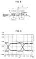
- FIG. 1illustrates an example known memory module 1 including a command-address register (CAR) 3 and a plurality of dynamic random access memories (DRAM) 2 as memory chips.
- CARcommand-address register
- DRAMdynamic random access memories
- This drawingillustrates the topology of command-address (CA) wiring of the memory module 1 .
- the DRAMs 2 of this memory module 1are double-data-rate synchronous (DDR-S) DRAMs.
- the DRAMs 2are divided into two groups.
- One of the two groupsincludes four DRAMs 2 on one surface of a package substrate and four DRAMs 2 on the other surface thereof.
- the other of the two groupsincludes five DRAMs 2 on one surface of the package substrate and five DRAMs 2 on the other surface thereof.
- the above-described topologyis provided for reducing the length of the CA wiring so as to reduce the area on which the CA wiring is provided. According to this configuration, however, the length of a stub increases. Subsequently, the time constant of signal reflections becomes large. Therefore waveforms obtained where a high-speed signal is transmitted through this wiring are significantly distorted by multiple reflections, as shown in FIG. 2 .
- the above-described known memory modulehas a problem that the waveforms thereof are significantly distorted due to a high-speed signal.
- the problemis caused by the configuration of the memory module. That is to say, the DRAMs functioning as memory chips are divided into two groups and these two groups are connected to each other via the wiring with a T-branch structure. Since the length of the stub increases, the time constant of signal reflections increases and the distortion of waveforms becomes significant.
- JP-AJapanese Unexamined Patent Application Publication
- a memory modulecomprises a module substrate, at least one command-address signal register, a plurality of memory chips provided on a top face and under face of the module substrate, each of the plurality of memory chips having a command-address signal terminal with an active-termination circuit, and command-address signal wiring.
- the command-address signal registeris internally wired and connected to the plurality of memory chips.
- the plurality of memory chipsis divided so as to form at least one 1 -ranked memory group including two or three memory chips that are provided on one face and the other face of the module substrate and near and adjacent to each other and at least one 2-ranked memory group including two or three memory chips that are provided on one face and the other face of the module substrate and near and adjacent to each other.
- the 1 -ranked memory groupis paired with the 2-ranked memory group adjacent thereto so that this pair of memory groups has four or five memory chips. This pair of memory groups is accessible at the same time.
- the command-address signal wiringhas a T-branch structure and is used for connecting the command-address signal register to the pair of memory groups corresponding thereto.
- the command-address signal terminals of the memory chips of the memory group that is not used during the accessare actively terminated. That is to say, the command-address signal terminals of the memory chips of either the 1-ranked memory group or the 2-ranked memory group are actively terminated.
- the memory modulehas other signal wiring with the same structure as that of this command-address signal wiring.
- the above-described memory modulefurther comprises data signal wiring with a T-branch structure for connecting one of the pair of memory groups to the other.
- Each of the plurality of memory chipsmay further have a data signal terminal. The data-signal terminals of the memory chips of the memory group that is not used during the access may be actively terminated.
- the memory modulefurther comprises command-address active-termination control signal wiring connected to a module terminal corresponding to any of the memory groups.
- the memory modulefurther comprises clock-signal wiring with a T-branch structure.
- Each of the plurality of memory chipsmay further have a clock signal terminal.
- An even-number of the command-address signal registersmay be provided so as to form at least two groups.
- the clock signal wiringmay be connected to the command-address signal registers and the memory chips so as to connect the at least two groups of command-address signal registers to each other and the pair of memory groups to each other.
- the clock-signal terminals of the memory chips of one of the pair of memory groupsmay be actively terminated.
- each memory group of at least one of the pairs of memory groups adjacent and connected to each other so as to form a T-branch structurehas two stacked memory chips on one face of the module substrate and one memory chip on the other face of the module substrate.
- the command-address signal terminal of the memory chip on the other facemay be actively terminated.
- pairs of the memory groups with ECC (error checking and correcting) capabilityare provided.
- These four pairs of the memory groupsmay include six memory groups.
- Each of the six memory groupsmay have one memory chip on one face of the module substrate and another memory chip on the other face thereof.
- These four pairs of the memory groupsmay further include two memory groups.
- Each of the two memory groupsmay have two memory chips stacked on each other on one face of the module substrate and another memory chip on the other face thereof.
- the stacked memory chipsinclude a single memory chip with a first pad provided on one face of a printed circuit board and another single memory chip with a second pad provided on the other face thereof.
- the command-address signal wiringmay be connected to both the first and second pads through a single wire and the data-signal wiring may be connected to one of the first and second pads through another single wire.
- a signal line of the stacked memory chipsmay be sandwiched between a power layer and a ground layer so as to form a strip line.
- the memory modulefurther comprises clock-signal wiring with a T-branch structure for connecting one of the memory groups paired with each other to the other. Memory chips of one of the pair of memory groups may be terminated.
- each of the plurality of memory chipsfurther has an active-termination circuit for a command-address active-termination control signal, a circuit for latching the command-address active-termination control signal, and a circuit for turning at least part of the active-termination circuit when the command-address active-termination control signal is latched during the active-termination circuit is turned on.
- a memory systemcomprises a mother board, first and second memory modules that have been described above on the mother board, and a memory controller connected to a plurality of memory chips mounted on the first and second memory modules so as to control memory capability.
- a signal wirings between each of the memory modules and the memory controllermay be independently connected therebetween.
- the first memory moduleis provided at a first distance from the memory controller and the second memory module is provided at a second distance longer than the first distance from the memory controller.
- Signal wiring from the first memory module to the memory controllermay be formed as internal-layer wiring and signal wiring from the second memory module to the memory controller may be formed as surface-layer wiring.
- a memory systemcomprises a mother board, first and second memory modules that have been described above on the mother board, and a memory controller connected to a plurality of memory chips mounted on the first and second memory modules so as to control memory capability.
- a memory controllerconnected to a plurality of memory chips mounted on the first and second memory modules so as to control memory capability.
- signal wirings between each of the memory modules and the memory controllerat least one of the command-address signal and the clock signal may be connected through wiring with a T-branch structure.
- the configuration of the memory module of the present inventionallows for reducing the waveform distortion during writing and/or reading a high-speed signal and achieving memory capability with reliability.
- FIG. 1illustrates example block wiring used for a known memory module
- FIG. 2illustrates example simulation waveforms obtained where the known memory module shown in FIG. 1 is used.
- FIG. 3illustrates an example configuration and example block wiring of a memory module according to the present invention
- FIG. 4Aillustrates an example VTT active-termination circuit that can be used for the present invention
- FIG. 4Billustrates an example center-tap active-termination circuit that can be used for the present invention
- FIG. 5illustrates an example configuration of a memory system according to the present invention
- FIG. 6illustrates example signal wiring of the memory system
- FIG. 7is a time chart illustrating an example operation performed by the memory module
- FIG. 8schematically illustrates example wiring with a T-branch structure that can be used for the memory module
- FIG. 9illustrates example simulation waveforms obtained at a measuring point shown in FIG. 8 ;
- FIG. 10is a schematic diagram illustrating an example where active termination is performed in all DRAMs shown in FIG. 8 ;
- FIG. 11illustrates example simulation waveforms obtained at a measuring point shown in FIG. 10 ;
- FIG. 12is a schematic diagram illustrating an example where a position at which active termination is performed is moved from the DRAM on the signal-non-reception side of FIG. 8 to a DRAM on the signal-reception side;
- FIG. 13illustrates example simulation waveforms obtained at a measuring point shown in FIG. 12 ;
- FIG. 14illustrates another example configuration and block wiring of the memory module different from those of FIG. 3 in that eighteen DRAMs including fourteen DRAMs and two units of two DRAMs stacked on each other are used;
- FIG. 15illustrates example wiring with a T-branch structure that can be used for the memory module shown in FIG. 14 ;
- FIG. 16illustrates example simulation waveforms obtained at a measuring point shown in FIG. 15 ;
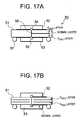
- FIG. 17Aillustrates an example topology of signal wiring used for a package substrate of the stacked DRAMs shown in FIG. 14 ;
- FIG. 17Billustrates another example topology of signal wiring used for the package substrate of the stacked DRAMs shown in FIG. 14 ;
- FIG. 18illustrates an example topology of CA-signal wiring shown in FIG. 14 ;
- FIG. 19illustrates an example topology of DQ-signal wiring shown in FIG. 14 ;
- FIG. 20illustrates another example configuration and block wiring of the memory module of the present invention where eighteen DRAMs different from those shown in FIG. 14 are used;
- FIG. 21illustrates another example configuration and block wiring of the memory module of the present invention wherein eighteen DRAMs different from those shown in FIGS. 14 and 20 are used;
- FIG. 22illustrates another example configuration and block wiring different from those shown in FIGS. 3, 14 , 20 , and 21 of the memory module of the present invention
- FIG. 23illustrates example clock-signal wiring used for the memory module of the present invention
- FIG. 24illustrates example block wiring used for another memory system according to the present invention, the memory system being different from that shown in FIG. 6 ;
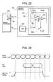
- FIG. 25illustrates an example CA active-termination control circuit used for the memory system of the present invention
- FIG. 26is a time chart illustrating an example operation performed by another memory module according to the present invention shown in FIG. 25 ;
- FIG. 3is a block wiring diagram illustrating a first embodiment of the present invention.
- a memory module 10includes 11-1-ranked and 11-2-ranked devices that are accessible at the same time. These devices are sixteen dynamic random access memories (DRAMs) 12 . These DRAMs 12 are divided into two groups formed on both faces of a module substrate and each of the two groups includes eight DRAMs 12 . These eight DRAMs 12 are divided into four memory groups and each of the four memory groups includes two DRAMs. One of the two DRAMs is mounted on one face of the module substrate and the other is mounted on the other face thereof. These two DRAMs are commonly wired. Therefore, this drawing shows only eight DRAMs 12 . That is to say, each of the memory groups is paired with the other memory group adjacent thereto. Further, the rank of one of each pair of the adjacent memory groups is different from that of the other.
- DRAMsdynamic random access memories
- one DRAM 12 on the top surface of the module substrateis paired with another DRAM 12 on the under surface thereof so as to form one memory group.
- One of the pair of adjacent memory groupsis 11-1-ranked and the other is 11-2 ranked. That is to say, the memory groups are provided so that the rank of one of adjacent memory groups is different from that of the other.
- the DRAMs 12may be provided on the top surface and under surface of the module substrate so as to be adjacent and close to one another. In this case, adjacent two memory groups function as one unit.
- One of the two adjacent memory groupsmay include two or three DRAMs 12 so that the two adjacent memory groups include four or five DRAMs 12 .
- Each of the DRAMs 12has a command-address (CA) signal terminal, a data (DQ) signal terminal, a CA-active termination control (ODT-CA) signal terminal, and a clock (WCLK) signal terminal.
- the CA signal terminalhas an active-termination circuit.
- the memory module 10further has four CA-signal registers (CARs) 13 so as to divide the DRAMs 12 into two groups.
- the CARs 13are mounted on the top surface and under surface of the module substrate and commonly wired. Therefore, this drawing shows two CARs 13 .
- Each of the CARs 13has two CA-signal input terminals, a CA-signal output terminal, and a WCLK-signal terminal.
- CA-signal wiring between the DRAMs 12 and the CARs 13is established as below. Adjacent two memory groups including the DRAMs 12 are paired with each other and connected to each other through wiring with a T-branch structure. Where one of the pair of memory groups, for example, the 11-1-ranked memory group operates, the CA-signal terminals of the DRAMs 12 of the 11-2 ranked memory group are turned on and actively terminated.
- This T-branch structureallows for reducing the length of wiring from the adjacent DRAMs 12 to a branch point as much as possible. That is to say, the length of a stub can be reduced as much as possible.
- This branch pointis provided at a predetermined position so that the length of wiring of this pair of memory groups from the branch point to the CAR 13 becomes the same as that of another pair of memory groups adjacent thereto. Subsequently, significant waveform distortion can be prevented even though high-speed signals are input to the memory module 10 .
- DQ-signal wiringforms the T-branch structure so as to pair adjacent DRAMs 12 with each other and is terminated actively at a DRAM 12 adjacent to a DRAM 12 in operation.
- ODT-CA-signal wiring connected to each of the DRAMs 12extends from a module terminal corresponding to the DRAM 12 .
- WCLK-signal wiringis provided for each of the DRAMs 12 and each of the CARs 13 . That is to say, the WCLK-signal wiring has a T-branch structure so as to pair adjacent DRAMs 12 with each other and adjacent CARs 13 with each other.
- the WCLK-signal wiringhas two wires respectively connecting to the pair of adjacent DRAMs 12 or the pair of adjacent CARs 13 . One of the two wires is opened and the other is terminated.
- a CA active-termination circuit of the 2-ranked DRAM 12is turned on.
- another CA signalis transmitted from the CAR 13 to the 2-ranked DRAM 12
- a CA active-termination circuit of the 1-ranked DRAM 12 on one face of the module substrateis turned on.
- An effective termination resistance value of the active termination circuit of one of the DRAM 12 sis the same as that of characteristic impedance value of signal wiring connected thereto.
- FIGS. 4A and 4Bshow example active-termination circuits.
- FIG. 4Ashows a VTT active-termination circuit including a resistor Rterm connected to a termination power 21 via pass transistors 22 and 23 in parallel. Where the value of a termination voltage is one-second of a voltage V DDQ , the resistor Rterm should be connected to this termination power 21 . However, the termination voltage value of the VTT may be the same as that of V DDQ , as required.
- FIG. 4Bshows a center-tap active-termination circuit including transistors 22 and 23 in series and two resistors 2 ⁇ Rterm. A termination voltage is connected to a center tap between the transistors 22 and 23 and the two resistors 2 ⁇ Rterm. Another voltage source is not necessary where the value of the termination voltage is one-second of the voltage V DDQ , though the power consumption increases.
- a termination resistoris provided at the signal-input side of each of the CARs 13 .
- two memory modules 10 ( 1 ) and 10 ( 2 ) and a memory controller 31are mounted on a mother board 30 .
- a signal between terminals of the memory controller 31 and the memory module 10 ( 1 ) and a signal between the terminals of the memory controller 31 and the memory module 10 ( 2 )are independently wired and connected therebetween.
- the terminal of the memory module 10 ( 1 )is formed in a connector 32 ( 1 ) extending from the DRAMs 12 and the CARs 13 .
- the terminal of the memory module 10 ( 2 )is formed in a connector 32 ( 2 ) extending from the DRAMs 12 and the CARs 13 .
- the position at which the memory module 10 ( 1 ) is providedis closer to the memory controller 31 than the position at which the memory module 10 ( 2 ) is provided is.
- Wiring between the memory module 10 ( 1 ) and the memory controller 31is surface-layer wiring and wiring between the memory module 10 ( 2 ) and the memory controller 31 is internal-layer wiring, so that the length of wiring between the memory controller 31 and the connector 32 ( 1 ) is substantially the same as the length of wiring between the memory controller 31 and the connector 32 ( 2 ).
- a groundis provided between the surface-layer wiring and the internal-layer wiring as a ground layer. Further, a power layer is provided on an under face of the mother board 30 .
- FIG. 6shows part of the memory system. Main operations of the memory system will now be described with reference to FIG. 7 .
- the memory controller 31outputs the CA signal to the CAR 13 and an ODT_CA signal to the 2-ranked DRAM 12 over a time period including two clock cycles per every instruction in synchronization with a WCLK signal.
- This synchronizationis achieved by center aligning, that is to say, by providing a clock edge at the center of a period where data is valid.
- the CA signalis input to the CAR 13 and the active termination circuit of the 2-ranked DRAM 12 is turned on.
- the CAR 13outputs CA signals to the 1-ranked DRAM 12 .
- the 1-ranked DRAM 12receives each of the CA signals at an even-numbered edge indicated by an arrow of the WCLK signal.
- the ODT_CA signalis turned off when a period of time corresponding to one half cycle elapses after the last CA signal is output.
- a DQ active-termination circuit of the 2-ranked DRAM 12is turned on.
- the DQ signalis transferred to the 2-ranked DRAM 12 , only the active-termination circuit of the 1-ranked DRAM 12 on one face of the module substrate is turned on. This control is performed by a CA resistor.
- the DQ signalmay be transferred in synchronization with a DQ strobe signal as in the case of a known DDR-SDRAM. If the memory controller 31 has input-timing optimization capability, the DQ strobe signal may not be used.
- FIG. 8showing the configuration of part of the memory system
- FIG. 9showing simulation waveforms.
- the T-branch wiring according to the present inventionis formed between adjacent DRAMs 12 , the length of a stub is relatively short, for example, a little over ten millimeters. Therefore, if signal reflections occur at the open end of the 1-ranked DRAM 12 during signal reception, the waveforms are prevented from being significantly distorted due to a small time constant. Conversely, fine waveforms can be obtained by moderate signal reflections.
- the wiring connected to the 1-ranked DRAM 12 on the signal-reception sideforms an open end. Therefore, signal reflections occur and the rise and fall of signal waveforms become sharp, whereby improved signal waveforms can be obtained.
- FIG. 10is a schematic diagram showing an example configuration of part of the memory module and FIG. 11 shows example signal waveforms obtained when the 1-ranked DRAM 12 on the signal-reception side is terminated.
- a signaldirectly reaches the terminated part, and a reflected signal reaches the terminated part with a predetermined delay. Therefore, the rise and fall of the signal waveforms become blunt.
- FIG. 12is a schematic diagram showing another example configuration of part of the memory module and FIG. 13 shows example signal waveforms obtained when the 1-ranked DRAM 12 on the signal-reception side is terminated.
- a signaldirectly reaches the terminated part, and a reflected signal reaches the terminated part with a predetermined delay. Therefore, the rise and fall of the signal waveforms become blunt.
- the above-described wiringis used for transmitting and receiving CA signals between the DRAM 12 and the CAR 13 .
- the wiringcan be used for transmitting and receiving signals between the DRAM 12 and an element other than the CAR 13 .
- a PLL (phase-locked-loop) circuitcan be used for transmitting and receiving a WCLK signal.
- any part of this memory modulecan be replaced with another part as long as the above-described capabilities of the present invention can be achieved.
- FIGS. 14 to 19A second embodiment of the present invention will now be described with reference to FIGS. 14 to 19 .
- eighteen DRAMs 12are used, as shown in FIG. 14 . That is to say, two DRAMs 12 are added to the DRAMs 12 of the first embodiment. These two added DRAMs 12 are stacked on a predetermined 1-ranked DRAM 12 and a predetermined 2-ranked DRAM 12 being adjacent thereto and paired therewith, whereby two units of two DRAMs stacked on each other are formed.
- One of the two units of the stacked DRAMs 12is provided on one face of the module substrate and a DRAM 12 is provided on the other face thereof so as to form a memory group.
- the other of the two units of the stacked DRAMs 12 on one face of the module substrate and another DRAM 12 on the other face thereofalso form another memory group.
- FIG. 16shows simulation waveforms obtained by the above-described configuration. These simulation waveforms are a little blunter than the simulation waveforms shown in FIG. 9 but sharper than those shown in FIGS. 11 and 13 .
- FIGS. 17A and 17Bshows example signal wiring formed in stacked DRAMs 50 according to this embodiment.
- the stacked DRAMs 50includes DRAMs 52 and 53 formed as memory chips.
- the DRAM 52is provided on one face of a printed circuit board 51 and the DRAM 53 is provided on the other face thereof. That is to say, signal wiring extending from a ball terminal 57 is connected to a pad 54 of the DRAM 52 and a pad 55 of the DRAM 53 through a via hole 56 .
- a signal layeris connected to the pads 55 and 54 .
- a voltage V DDQ layeris formed on one face of the printed circuit board 51 and a voltage V SSQ layer is formed on the other face thereof.
- the signal wiring of the stacked DRAMs 50is provided between a power layer and a ground layer so as to form a strip line. Subsequently, the quantity of noise on signals decreases.
- a signal layeris connected to the pads 54 and 55 and externally connected to one of the DRAMs 52 and 53 .
- the signal layeris externally connected to the DRAM 53 .
- the voltage V DDQ layer and the voltage V SSQ layerare formed between internal layers of the printed circuit board 51 . Since the power layer and the ground layer are provided so as to be adjacent to each other, a loop inductance between the power and the ground decreases, and the noise quantity in the power and the ground reduces.
- FIG. 18shows wiring for taking out a CA signal of the stacked DRAMs 50 .
- the CA signal of the stacked DRAMs 50is taken out from an internal layer of the printed circuit board 51 , as shown in FIG. 17A . Then, the CA signal is transmitted to a module substrate 61 . Further, a CA signal of a DRAM 63 provided on an under face of the stacked DRAMs 50 is taken out from an internal layer of a package substrate 62 and transmitted to the module substrate 61 . That is to say, the CA-signal wiring is connected to both the DRAMs 50 and 63 .
- the length of this CA-signal wiringshould be reduced so as to be smaller than that of CA-signal wiring with a different configuration so as to synchronize the timing of this CA signal with the timing of other CA signals.
- FIG. 19illustrates wiring for taking out DQ signals of the stacked DRAMs 50 .
- the positions at which the stacked DRAMs 50 and the DRAM 63 are providedare the same as those shown in FIG. 18 .
- each of the DQ signalsis separately taken out from pads of the DRAMs 52 , 53 , and 63 . That is to say, the DQ-signal wiring is formed of a single wire and connected to the pads. Each of the pads is provided on one face of each of the DRAMs.
- a third embodiment of the present inventionwill now be described with reference FIG. 20 .
- eighteen DRAMs with ECC (error checking and correcting) capability different from the DRAMs shown in FIG. 14are used.
- a memory module 70includes a plurality of 71 -ranked devices. These 71 -ranked devices comprise nine DRAMs 72 on a top face of a module substrate and nine DRAMs 72 on an under face thereof. A fifth DRAM 72 on the top face, that is, the DRAM 72 at the center of the top face is 2-ranked. On the other hand, a fifth DRAM 72 on the under face, that is, the DRAM 72 at the center of the under face is 1-ranked. These first to ninth DRAMs 72 on the top face are designated by reference character A, and these first to ninth DRAMs 72 on the under face are designated by reference character B.
- the DRAMs 1 A, 1 B, 3 A, 3 B, 5 B, 6 A, 6 B, 8 A, and 8 Bare 1-ranked.
- the DRAMs 2 A, 2 B, 4 A, 4 B, 5 A, 7 A, 7 B, 9 A, and 9 Bare 2-ranked.
- Adjacent memory groups at the center of the memory module 70are paired with each other.
- the pair of adjacent memory groupsincludes the 1-ranked DRAMs 5 B, 6 A, and 6 B, and the 2-ranked DRAMs 7 A and 7 B.
- Other adjacent memory groups at the center of the memory module 70are also paired with each other.
- This pair of adjacent memory groupsincludes the 1-ranked DRAMs 3 A and 3 B, and the 2-ranked DRAMs 4 A, 4 B, and 5 A.
- Each of these pairs of adjacent memory groupshas a T-branch structure as in the above-described embodiments.
- a CA active-termination circuit of each of the 2-ranked DRAMs 72is turned on.
- a CA active-termination circuit of the 1-ranked DRAM 72 on one face of the module substrateis turned on.
- Zmindicates the characteristic impedance of the mother-board wiring.
- Z 0indicates the characteristic impedance of the memory-module wiring.
- FIG. 21shows eighteen DRAMs with ECC capability. These DRAMs are different from those shown in FIGS. 14 and FIG. 20 .
- a memory module 80includes 81 -ranked devices. These 81 -ranked devices comprise nine DRAMs 82 on a top face of a module substrate and nine DRAMs 82 on an under face thereof, as in the case of FIG. 20 . Every three memory groups adjacent to one another include at least one 1-ranked memory group and at least one 2-ranked memory group. DRAMs 82 of a memory group at the center of these three memory groups are provided on the top face and under face of the module substrate, as described above. One of these DRAMs 82 of this center memory group is 1 -ranked and the other is 2-ranked.
- first to ninth DRAMs 82 on the top faceare designated by reference character A
- first to ninth DRAMs 82 on the under faceare designated by reference character B.
- a first CA-signal line extending from the DRAMs 1 A to 3 A and the DRAMS 1 B to 3 Bis connected to a CAR 83 - 1 .
- a second CA-signal line extending from the DRAMs 7 A to 9 A and the DRAMS 7 B to 9 Bis connected to a CAR 83 - 2 .
- a third CA-signal line extending from the DRAMs 4 A to 6 A and the DRAMs 4 B to 6 Bare connected to the CAR 83 - 1 or to the CAR 83 - 2 .
- the third and fourth linescan be connected to both the CARs 83 - 1 and 83 - 2 , as required.
- nine 81 -ranked devices or nine DRAMs 82 on each face of the module substrateare divided into three groups.
- the wiring configurations of these three groupsare the same as one another, so that the lengths of lines of these three groups are the same as one another. Subsequently, variations in the waveforms of the three groups are reduced.
- a fifth embodiment of the present inventionwill now be described with reference to FIG. 22 .
- Nine DRAMs with ECC capabilityare used in this embodiment.
- This drawingalso shows a memory module 90 including 91 -ranked devices that will be described as below.
- the above-described nine DRAMsare provided at predetermined positions corresponding to the positions shown in FIG. 14 at which the 1-ranked DRAMs are provided. Seven of these nine DRAMs are provided as DRAMs 92 and two thereof are stacked on each other and provided as stacked DRAMs 93 . Further, fixed resistors Rf are provided in place of DRAMs at predetermined positions corresponding to the positions shown in FIG. 14 at which the 2-ranked DRAMs are provided and paired with the DRAMs adjacent thereto. The positions of CARs 94 and signal lines are same as in the case of FIG. 14 .
- FIG. 23A sixth embodiment relating to clock-signal wiring of the present invention will now be described with reference to FIG. 23 .
- a PLL circuit 101is used in place of the above-described CA registers so as to generate clock signals that are connected to the DRAMs.
- This clock-signal wiringhas a T-branch structure so that adjacent DRAMs are paired with each other. Termination is performed in DRAMs on the signal-non-reception side.
- the internal-layer wiringis used as the signal wiring extending from the memory controller to the memory module close thereto.
- the surface-layer wiringis used as the signal wiring extending from the memory controller to the other memory module far therefrom.
- the above-described two memory modulesare accessible at the same time. If accesses are made to the above-described memory modules through two lines and time required for transmitting a signal through one of the lines is the same as that of the other, the timing of inputting a signal to the memory controller through one of the lines differs from the timing of inputting another signal to the memory controller through the other line during signal reading. This difference reduces timing margins of the memory system.
- the time required for transmitting a signal through the surface-layer wiringis about 6 ns/m and that for transmitting a signal through the internal-layer wiring is about 7 ns/m. That is to say, the time required for transmitting a signal through the internal-layer wiring is longer than that in the case where a signal is transmitted through the surface-layer wiring.
- the length of signal wiring extending from the memory controller 31 to the memory module close theretois about 100 millimeters and the length of signal wiring extending from the memory controller 31 to the memory module far therefrom is about 120 millimeters.
- the internal-layer wiringis used as the signal wiring from the memory controller 31 to the memory module close thereto and the surface-layer wiring is used as the signal wiring from the memory controller 31 to the memory module far therefrom. Consequently, the time required for transmitting a signal from the memory controller 31 to the memory module close thereto becomes the same as the time required for transmitting a signal from the memory controller 31 to the memory module far therefrom, whereby the amount of input-timing-margin reduction of the memory controller 31 during signal reading can be reduced.
- FIG. 24shows a memory system whose configuration is different from that of the memory system shown in FIG. 6 .
- This memory systemhas a memory controller 113 , a memory module 110 ( 1 ) including two DRAMs, a CAR, and a PLL circuit, and a memory module 110 ( 2 ) including two DRAMs, a CAR, and a PLL circuit.
- signal wiring between the memory controller 113 and the two DRAMs of the memory module 110 ( 1 )may have a T-branch structure.
- Signal wiring extending from the two DRAMs of the memory module 110 ( 1 ) to the CAR thereofmay also have a T-branch structure.
- signal wiring between the memory controller 113 and the two DRAMs of the memory module 110 ( 2 )may have a T-branch structure.
- Signal wiring extending from the two DRAMs of the memory module 110 ( 2 ) to the CAR thereofmay also have a T-branch structure.
- an ODT_CA signal transmitted from a memory controller 130is connected to a latch circuit 122 in a DRAM 121 of a memory module 120 .
- An output signal from the latch circuit 122functions as an ODT_CA active-termination control signal.
- a termination circuit 123is terminated at a ground.
- the termination circuit 123is terminated at the voltage V DDQ .
- the termination circuit 123is also terminated at the voltage V DDQ during transition of the ODT_CA signal from the power-voltage level H to the ground level L.
- the termination circuit 123is terminated at the ground when the ODT_CA signal reaches the ground level L.
- the memory controller 130has an ODT_CA-signal output circuit 131 including an output resistor Ron.
- the resistance value of the output resistor Ronis matched to the value of a characteristic impedance Z 0 of ODT_CA-signal wiring for reducing noises caused by signal reflections. Subsequently, the resistance value Ron becomes equal to the characteristic impedance Z 0 .
- This output resistor Ronterminates an output terminal of the ODT_CA-signal output circuit 131 .
- an ODT_CA signalis latched to the power-voltage level H or the ground level L according to the level of the ODT_CA signal. If the ODT_CA signal is latched to the power-voltage level H, an ODT_CA active terminal 124 on the ground side is turned off. If the ODT_CA signal is latched to the ground level L, the ODT_CA active terminal 124 on the power-voltage side is turned off. In both cases, no currents flow into the ODT_CA active terminal 124 and the power consumption of the DRAM 121 reduces.
Landscapes
- Dram (AREA)
- Memory System (AREA)
Abstract
Description
- 1. Field of the Invention
- The present invention relates to a memory module including at least one command-address signal register and a plurality of memory chips. Each of the memory chips has a command-address signal terminal with an active-termination circuit. The memory chips are divided into a plurality of memory groups of even-numbered ranks. The command-address signal register is connected to the plurality of memory chips through internal wiring. The present invention further relates to a memory system using the above-described memory module and particularly relates to a memory module that can reduce signal reflections in a stub with a T-branch structure and operate with high speed and a memory system using this memory module.
- 2. Description of the Related Art
FIG. 1 illustrates an example knownmemory module 1 including a command-address register (CAR)3 and a plurality of dynamic random access memories (DRAM)2 as memory chips. This drawing illustrates the topology of command-address (CA) wiring of thememory module 1. TheDRAMs 2 of thismemory module 1 are double-data-rate synchronous (DDR-S) DRAMs.- In the
memory module 1, theDRAMs 2 are divided into two groups. One of the two groups includes fourDRAMs 2 on one surface of a package substrate and fourDRAMs 2 on the other surface thereof. The other of the two groups includes fiveDRAMs 2 on one surface of the package substrate and fiveDRAMs 2 on the other surface thereof. These two groups ofDRAMs 2 and theCAR 3 are connected to each other through the CA wiring with a T-branch structure. - The above-described topology is provided for reducing the length of the CA wiring so as to reduce the area on which the CA wiring is provided. According to this configuration, however, the length of a stub increases. Subsequently, the time constant of signal reflections becomes large. Therefore waveforms obtained where a high-speed signal is transmitted through this wiring are significantly distorted by multiple reflections, as shown in
FIG. 2 . - The above-described known memory module has a problem that the waveforms thereof are significantly distorted due to a high-speed signal.
- The problem is caused by the configuration of the memory module. That is to say, the DRAMs functioning as memory chips are divided into two groups and these two groups are connected to each other via the wiring with a T-branch structure. Since the length of the stub increases, the time constant of signal reflections increases and the distortion of waveforms becomes significant.
- Such related technique is disclosed in, for example, Japanese Unexamined Patent Application Publication (JP-A) No. 2001-270518.
- Accordingly, it is an object of the present invention to provide a memory module, a plurality of memory chips used therefor, and a memory system using the memory module and the plurality of memory chips so as to solve the above-described problem and reduce the waveform distortion due to a high-speed signal.
- A memory module according to one aspect of the present invention comprises a module substrate, at least one command-address signal register, a plurality of memory chips provided on a top face and under face of the module substrate, each of the plurality of memory chips having a command-address signal terminal with an active-termination circuit, and command-address signal wiring. The command-address signal register is internally wired and connected to the plurality of memory chips.
- The plurality of memory chips is divided so as to form at least one1-ranked memory group including two or three memory chips that are provided on one face and the other face of the module substrate and near and adjacent to each other and at least one 2-ranked memory group including two or three memory chips that are provided on one face and the other face of the module substrate and near and adjacent to each other. The1-ranked memory group is paired with the 2-ranked memory group adjacent thereto so that this pair of memory groups has four or five memory chips. This pair of memory groups is accessible at the same time. The command-address signal wiring has a T-branch structure and is used for connecting the command-address signal register to the pair of memory groups corresponding thereto. When access is made, one of the pair of memory groups is used during the access and the other is not used. The command-address signal terminals of the memory chips of the memory group that is not used during the access are actively terminated. That is to say, the command-address signal terminals of the memory chips of either the 1-ranked memory group or the 2-ranked memory group are actively terminated. The memory module has other signal wiring with the same structure as that of this command-address signal wiring.
- According to the topology of the above-described signal wiring with the T-branch structure, memory chips close and/or adjacent to each other on one face or both faces of the module substrate are paired with each other. Therefore, the length of a stub decreases. Active termination is performed in the memory chips of a memory group on the signal-non-reception side, the memory group being one of the pair of memory groups connected to each other via the command-address signal wiring with the T-branch structure. Therefore, the wiring of the memory chips of a memory group on the signal-reception side, the memory group being the other of the pair of memory groups, functions as an open end. Therefore, if signal reflections occur at the open end on the signal-reception side, the time constant thereof is small. Subsequently, the waveforms are prevented from being significantly distorted. Conversely, moderate signal reflections achieve fine waveforms with sharp rise and fall.
- Preferably, the above-described memory module further comprises data signal wiring with a T-branch structure for connecting one of the pair of memory groups to the other. Each of the plurality of memory chips may further have a data signal terminal. The data-signal terminals of the memory chips of the memory group that is not used during the access may be actively terminated.
- Preferably, the memory module further comprises command-address active-termination control signal wiring connected to a module terminal corresponding to any of the memory groups.
- Preferably, the memory module further comprises clock-signal wiring with a T-branch structure. Each of the plurality of memory chips may further have a clock signal terminal. An even-number of the command-address signal registers may be provided so as to form at least two groups. The clock signal wiring may be connected to the command-address signal registers and the memory chips so as to connect the at least two groups of command-address signal registers to each other and the pair of memory groups to each other. The clock-signal terminals of the memory chips of one of the pair of memory groups may be actively terminated.
- Preferably, each memory group of at least one of the pairs of memory groups adjacent and connected to each other so as to form a T-branch structure has two stacked memory chips on one face of the module substrate and one memory chip on the other face of the module substrate. The command-address signal terminal of the memory chip on the other face may be actively terminated.
- Preferably, four pairs of the memory groups with ECC (error checking and correcting) capability are provided. These four pairs of the memory groups may include six memory groups. Each of the six memory groups may have one memory chip on one face of the module substrate and another memory chip on the other face thereof. These four pairs of the memory groups may further include two memory groups. Each of the two memory groups may have two memory chips stacked on each other on one face of the module substrate and another memory chip on the other face thereof.
- Preferably, the stacked memory chips include a single memory chip with a first pad provided on one face of a printed circuit board and another single memory chip with a second pad provided on the other face thereof. The command-address signal wiring may be connected to both the first and second pads through a single wire and the data-signal wiring may be connected to one of the first and second pads through another single wire. A signal line of the stacked memory chips may be sandwiched between a power layer and a ground layer so as to form a strip line.
- Preferably, the memory module further comprises clock-signal wiring with a T-branch structure for connecting one of the memory groups paired with each other to the other. Memory chips of one of the pair of memory groups may be terminated.
- Preferably, each of the plurality of memory chips further has an active-termination circuit for a command-address active-termination control signal, a circuit for latching the command-address active-termination control signal, and a circuit for turning at least part of the active-termination circuit when the command-address active-termination control signal is latched during the active-termination circuit is turned on.
- A memory system according to another aspect of the present invention comprises a mother board, first and second memory modules that have been described above on the mother board, and a memory controller connected to a plurality of memory chips mounted on the first and second memory modules so as to control memory capability. A signal wirings between each of the memory modules and the memory controller may be independently connected therebetween.
- Preferably, the first memory module is provided at a first distance from the memory controller and the second memory module is provided at a second distance longer than the first distance from the memory controller. Signal wiring from the first memory module to the memory controller may be formed as internal-layer wiring and signal wiring from the second memory module to the memory controller may be formed as surface-layer wiring.
- A memory system according to another aspect of the present invention comprises a mother board, first and second memory modules that have been described above on the mother board, and a memory controller connected to a plurality of memory chips mounted on the first and second memory modules so as to control memory capability. Among signal wirings between each of the memory modules and the memory controller, at least one of the command-address signal and the clock signal may be connected through wiring with a T-branch structure.
- The configuration of the memory module of the present invention allows for reducing the waveform distortion during writing and/or reading a high-speed signal and achieving memory capability with reliability.
FIG. 1 illustrates example block wiring used for a known memory module; andFIG. 2 illustrates example simulation waveforms obtained where the known memory module shown inFIG. 1 is used.FIG. 3 illustrates an example configuration and example block wiring of a memory module according to the present invention;FIG. 4A illustrates an example VTT active-termination circuit that can be used for the present invention;FIG. 4B illustrates an example center-tap active-termination circuit that can be used for the present invention;FIG. 5 illustrates an example configuration of a memory system according to the present invention;FIG. 6 illustrates example signal wiring of the memory system;FIG. 7 is a time chart illustrating an example operation performed by the memory module;FIG. 8 schematically illustrates example wiring with a T-branch structure that can be used for the memory module;FIG. 9 illustrates example simulation waveforms obtained at a measuring point shown inFIG. 8 ;FIG. 10 is a schematic diagram illustrating an example where active termination is performed in all DRAMs shown inFIG. 8 ;FIG. 11 illustrates example simulation waveforms obtained at a measuring point shown inFIG. 10 ;FIG. 12 is a schematic diagram illustrating an example where a position at which active termination is performed is moved from the DRAM on the signal-non-reception side ofFIG. 8 to a DRAM on the signal-reception side;FIG. 13 illustrates example simulation waveforms obtained at a measuring point shown inFIG. 12 ;FIG. 14 illustrates another example configuration and block wiring of the memory module different from those ofFIG. 3 in that eighteen DRAMs including fourteen DRAMs and two units of two DRAMs stacked on each other are used;FIG. 15 illustrates example wiring with a T-branch structure that can be used for the memory module shown inFIG. 14 ;FIG. 16 illustrates example simulation waveforms obtained at a measuring point shown inFIG. 15 ;FIG. 17A illustrates an example topology of signal wiring used for a package substrate of the stacked DRAMs shown inFIG. 14 ;FIG. 17B illustrates another example topology of signal wiring used for the package substrate of the stacked DRAMs shown inFIG. 14 ;FIG. 18 illustrates an example topology of CA-signal wiring shown inFIG. 14 ;FIG. 19 illustrates an example topology of DQ-signal wiring shown inFIG. 14 ;FIG. 20 illustrates another example configuration and block wiring of the memory module of the present invention where eighteen DRAMs different from those shown inFIG. 14 are used;FIG. 21 illustrates another example configuration and block wiring of the memory module of the present invention wherein eighteen DRAMs different from those shown inFIGS. 14 and 20 are used;FIG. 22 illustrates another example configuration and block wiring different from those shown inFIGS. 3, 14 ,20, and21 of the memory module of the present invention;FIG. 23 illustrates example clock-signal wiring used for the memory module of the present invention;FIG. 24 illustrates example block wiring used for another memory system according to the present invention, the memory system being different from that shown inFIG. 6 ;FIG. 25 illustrates an example CA active-termination control circuit used for the memory system of the present invention;FIG. 26 is a time chart illustrating an example operation performed by another memory module according to the present invention shown inFIG. 25 ;- Embodiments of the present invention will now be described with reference to the attached drawings. The drawings are simplified for the sake of understanding so as to show main elements of the present invention.
FIG. 3 is a block wiring diagram illustrating a first embodiment of the present invention. As shown in this drawing, amemory module 10 includes 11-1-ranked and 11-2-ranked devices that are accessible at the same time. These devices are sixteen dynamic random access memories (DRAMs)12. TheseDRAMs 12 are divided into two groups formed on both faces of a module substrate and each of the two groups includes eightDRAMs 12. These eightDRAMs 12 are divided into four memory groups and each of the four memory groups includes two DRAMs. One of the two DRAMs is mounted on one face of the module substrate and the other is mounted on the other face thereof. These two DRAMs are commonly wired. Therefore, this drawing shows only eightDRAMs 12. That is to say, each of the memory groups is paired with the other memory group adjacent thereto. Further, the rank of one of each pair of the adjacent memory groups is different from that of the other.- Thus, according to this embodiment, one
DRAM 12 on the top surface of the module substrate is paired with anotherDRAM 12 on the under surface thereof so as to form one memory group. One of the pair of adjacent memory groups is 11-1-ranked and the other is 11-2 ranked. That is to say, the memory groups are provided so that the rank of one of adjacent memory groups is different from that of the other. However, theDRAMs 12 may be provided on the top surface and under surface of the module substrate so as to be adjacent and close to one another. In this case, adjacent two memory groups function as one unit. One of the two adjacent memory groups may include two or threeDRAMs 12 so that the two adjacent memory groups include four or fiveDRAMs 12. - Each of the
DRAMs 12 has a command-address (CA) signal terminal, a data (DQ) signal terminal, a CA-active termination control (ODT-CA) signal terminal, and a clock (WCLK) signal terminal. The CA signal terminal has an active-termination circuit. - The
memory module 10 further has four CA-signal registers (CARs)13 so as to divide theDRAMs 12 into two groups. As in the case of theDRAMs 12, theCARs 13 are mounted on the top surface and under surface of the module substrate and commonly wired. Therefore, this drawing shows twoCARs 13. Each of theCARs 13 has two CA-signal input terminals, a CA-signal output terminal, and a WCLK-signal terminal. - Next, the configuration of signal wiring and connection will be described with reference to this drawing.
- CA-signal wiring between the
DRAMs 12 and theCARs 13 is established as below. Adjacent two memory groups including theDRAMs 12 are paired with each other and connected to each other through wiring with a T-branch structure. Where one of the pair of memory groups, for example, the 11-1-ranked memory group operates, the CA-signal terminals of theDRAMs 12 of the 11-2 ranked memory group are turned on and actively terminated. - This T-branch structure allows for reducing the length of wiring from the
adjacent DRAMs 12 to a branch point as much as possible. That is to say, the length of a stub can be reduced as much as possible. This branch point is provided at a predetermined position so that the length of wiring of this pair of memory groups from the branch point to theCAR 13 becomes the same as that of another pair of memory groups adjacent thereto. Subsequently, significant waveform distortion can be prevented even though high-speed signals are input to thememory module 10. - DQ-signal wiring forms the T-branch structure so as to pair
adjacent DRAMs 12 with each other and is terminated actively at aDRAM 12 adjacent to aDRAM 12 in operation. - ODT-CA-signal wiring connected to each of the
DRAMs 12 extends from a module terminal corresponding to theDRAM 12. - As shown in this drawing, WCLK-signal wiring is provided for each of the
DRAMs 12 and each of theCARs 13. That is to say, the WCLK-signal wiring has a T-branch structure so as to pairadjacent DRAMs 12 with each other andadjacent CARs 13 with each other. The WCLK-signal wiring has two wires respectively connecting to the pair ofadjacent DRAMs 12 or the pair ofadjacent CARs 13. One of the two wires is opened and the other is terminated. - Where a CA signal is transmitted from the
CAR 13 to the 1-rankedDRAM 12, a CA active-termination circuit of the 2-rankedDRAM 12 is turned on. On the other hand, where another CA signal is transmitted from theCAR 13 to the 2-rankedDRAM 12, a CA active-termination circuit of the 1-rankedDRAM 12 on one face of the module substrate is turned on. - An effective termination resistance value of the active termination circuit of one of the DRAM12s is the same as that of characteristic impedance value of signal wiring connected thereto.
FIGS. 4A and 4B show example active-termination circuits.FIG. 4A shows a VTT active-termination circuit including a resistor Rterm connected to atermination power 21 viapass transistors termination power 21. However, the termination voltage value of the VTT may be the same as that of VDDQ, as required.FIG. 4B shows a center-tap active-terminationcircuit including transistors resistors 2×Rterm. A termination voltage is connected to a center tap between thetransistors resistors 2×Rterm. Another voltage source is not necessary where the value of the termination voltage is one-second of the voltage VDDQ, though the power consumption increases.- A termination resistor is provided at the signal-input side of each of the
CARs 13. - The configuration of a memory system will now be described with reference to
FIGS. 5, 6 , and3. - As shown in
FIG. 5 , two memory modules10(1) and10(2) and amemory controller 31 are mounted on amother board 30. A signal between terminals of thememory controller 31 and the memory module10(1) and a signal between the terminals of thememory controller 31 and the memory module10(2) are independently wired and connected therebetween. The terminal of the memory module10(1) is formed in a connector32(1) extending from theDRAMs 12 and theCARs 13. Further, the terminal of the memory module10(2) is formed in a connector32(2) extending from theDRAMs 12 and theCARs 13. - As shown in
FIG. 5 , the position at which the memory module10(1) is provided is closer to thememory controller 31 than the position at which the memory module10(2) is provided is. Wiring between the memory module10(1) and thememory controller 31 is surface-layer wiring and wiring between the memory module10(2) and thememory controller 31 is internal-layer wiring, so that the length of wiring between thememory controller 31 and the connector32(1) is substantially the same as the length of wiring between thememory controller 31 and the connector32(2). A ground is provided between the surface-layer wiring and the internal-layer wiring as a ground layer. Further, a power layer is provided on an under face of themother board 30. FIG. 6 shows part of the memory system. Main operations of the memory system will now be described with reference toFIG. 7 .- Where a CA signal is transmitted to the 1-ranked
DRAM 12, thememory controller 31 outputs the CA signal to theCAR 13 and an ODT_CA signal to the 2-rankedDRAM 12 over a time period including two clock cycles per every instruction in synchronization with a WCLK signal. This synchronization is achieved by center aligning, that is to say, by providing a clock edge at the center of a period where data is valid. Subsequently, the CA signal is input to theCAR 13 and the active termination circuit of the 2-rankedDRAM 12 is turned on. - Then, the
CAR 13 outputs CA signals to the 1-rankedDRAM 12. The 1-rankedDRAM 12 receives each of the CA signals at an even-numbered edge indicated by an arrow of the WCLK signal. The ODT_CA signal is turned off when a period of time corresponding to one half cycle elapses after the last CA signal is output. - Where a DQ signal is written into the 1-ranked
DRAM 12, a DQ active-termination circuit of the 2-rankedDRAM 12 is turned on. Where the DQ signal is transferred to the 2-rankedDRAM 12, only the active-termination circuit of the 1-rankedDRAM 12 on one face of the module substrate is turned on. This control is performed by a CA resistor. Where the DQ signal is read, the DQ signal may be transferred in synchronization with a DQ strobe signal as in the case of a known DDR-SDRAM. If thememory controller 31 has input-timing optimization capability, the DQ strobe signal may not be used. - Improved waveforms achieved by the present invention will now be described with reference to
FIG. 8 showing the configuration of part of the memory system andFIG. 9 showing simulation waveforms. - Since the T-branch wiring according to the present invention is formed between
adjacent DRAMs 12, the length of a stub is relatively short, for example, a little over ten millimeters. Therefore, if signal reflections occur at the open end of the 1-rankedDRAM 12 during signal reception, the waveforms are prevented from being significantly distorted due to a small time constant. Conversely, fine waveforms can be obtained by moderate signal reflections. - Where active termination is performed in the 2-ranked
DRAM 12 on the signal-non-reception side being one of theDRAMs 12 paired with each other through T-branch wiring, the wiring connected to the 1-rankedDRAM 12 on the signal-reception side forms an open end. Therefore, signal reflections occur and the rise and fall of signal waveforms become sharp, whereby improved signal waveforms can be obtained. FIG. 10 is a schematic diagram showing an example configuration of part of the memory module andFIG. 11 shows example signal waveforms obtained when the 1-rankedDRAM 12 on the signal-reception side is terminated. In this case, a signal directly reaches the terminated part, and a reflected signal reaches the terminated part with a predetermined delay. Therefore, the rise and fall of the signal waveforms become blunt.FIG. 12 is a schematic diagram showing another example configuration of part of the memory module andFIG. 13 shows example signal waveforms obtained when the 1-rankedDRAM 12 on the signal-reception side is terminated. As in the above-described case, a signal directly reaches the terminated part, and a reflected signal reaches the terminated part with a predetermined delay. Therefore, the rise and fall of the signal waveforms become blunt.- The above-described wiring is used for transmitting and receiving CA signals between the
DRAM 12 and theCAR 13. However, the wiring can be used for transmitting and receiving signals between theDRAM 12 and an element other than theCAR 13. For example, a PLL (phase-locked-loop) circuit can be used for transmitting and receiving a WCLK signal. - Without being limited to the above-described block diagrams, any part of this memory module can be replaced with another part as long as the above-described capabilities of the present invention can be achieved.
- A second embodiment of the present invention will now be described with reference to FIGS.14 to19.
- According to this embodiment, eighteen
DRAMs 12 are used, as shown inFIG. 14 . That is to say, twoDRAMs 12 are added to theDRAMs 12 of the first embodiment. These two addedDRAMs 12 are stacked on a predetermined 1-rankedDRAM 12 and a predetermined 2-rankedDRAM 12 being adjacent thereto and paired therewith, whereby two units of two DRAMs stacked on each other are formed. One of the two units of thestacked DRAMs 12 is provided on one face of the module substrate and aDRAM 12 is provided on the other face thereof so as to form a memory group. The other of the two units of thestacked DRAMs 12 on one face of the module substrate and anotherDRAM 12 on the other face thereof also form another memory group. According to this configuration, active termination is performed in theDRAMs 12 on the other face of the module substrate.FIG. 16 shows simulation waveforms obtained by the above-described configuration. These simulation waveforms are a little blunter than the simulation waveforms shown inFIG. 9 but sharper than those shown inFIGS. 11 and 13 . - Each of
FIGS. 17A and 17B shows example signal wiring formed instacked DRAMs 50 according to this embodiment. Thestacked DRAMs 50 includesDRAMs DRAM 52 is provided on one face of a printedcircuit board 51 and theDRAM 53 is provided on the other face thereof. That is to say, signal wiring extending from aball terminal 57 is connected to apad 54 of theDRAM 52 and apad 55 of theDRAM 53 through a viahole 56. - In
FIG. 17A , a signal layer is connected to thepads circuit board 51 and a voltage VSSQlayer is formed on the other face thereof. Thus, the signal wiring of thestacked DRAMs 50 is provided between a power layer and a ground layer so as to form a strip line. Subsequently, the quantity of noise on signals decreases. - In
FIG. 17B , a signal layer is connected to thepads DRAMs DRAM 53. The voltage VDDQlayer and the voltage VSSQlayer are formed between internal layers of the printedcircuit board 51. Since the power layer and the ground layer are provided so as to be adjacent to each other, a loop inductance between the power and the ground decreases, and the noise quantity in the power and the ground reduces. FIG. 18 shows wiring for taking out a CA signal of thestacked DRAMs 50. The CA signal of thestacked DRAMs 50 is taken out from an internal layer of the printedcircuit board 51, as shown inFIG. 17A . Then, the CA signal is transmitted to amodule substrate 61. Further, a CA signal of aDRAM 63 provided on an under face of thestacked DRAMs 50 is taken out from an internal layer of apackage substrate 62 and transmitted to themodule substrate 61. That is to say, the CA-signal wiring is connected to both theDRAMs stacked DRAMs 50 and the amount of time delay increase, the length of this CA-signal wiring should be reduced so as to be smaller than that of CA-signal wiring with a different configuration so as to synchronize the timing of this CA signal with the timing of other CA signals.FIG. 19 illustrates wiring for taking out DQ signals of thestacked DRAMs 50. The positions at which the stackedDRAMs 50 and theDRAM 63 are provided are the same as those shown inFIG. 18 . However, each of the DQ signals is separately taken out from pads of theDRAMs - A third embodiment of the present invention will now be described with reference
FIG. 20 . In this embodiment, eighteen DRAMs with ECC (error checking and correcting) capability different from the DRAMs shown inFIG. 14 are used. - As shown in this drawing, a
memory module 70 includes a plurality of71-ranked devices. These71-ranked devices comprise nineDRAMs 72 on a top face of a module substrate and nineDRAMs 72 on an under face thereof. Afifth DRAM 72 on the top face, that is, theDRAM 72 at the center of the top face is 2-ranked. On the other hand, afifth DRAM 72 on the under face, that is, theDRAM 72 at the center of the under face is 1-ranked. These first toninth DRAMs 72 on the top face are designated by reference character A, and these first toninth DRAMs 72 on the under face are designated by reference character B. - Subsequently, the DRAMs1A,1B,3A,3B,5B,6A,6B,8A, and8B are 1-ranked. Further, the DRAMs2A,2B,4A,4B,5A,7A,7B,9A, and9B are 2-ranked. Adjacent memory groups at the center of the
memory module 70 are paired with each other. The pair of adjacent memory groups includes the 1-ranked DRAMs5B,6A, and6B, and the 2-ranked DRAMs7A and7B. Other adjacent memory groups at the center of thememory module 70 are also paired with each other. This pair of adjacent memory groups includes the 1-ranked DRAMs3A and3B, and the 2-ranked DRAMs4A,4B, and5A. Each of these pairs of adjacent memory groups has a T-branch structure as in the above-described embodiments. - Where a CA signal is transferred from a
CAR 73 to the 1-rankedDRAMs 72, a CA active-termination circuit of each of the 2-rankedDRAMs 72 is turned on. Where another CA signal is transmitted from theCAR 73 to the 2-rankedDRAMs 72, a CA active-termination circuit of the 1-rankedDRAM 72 on one face of the module substrate is turned on. For achieving this embodiment, twoCARs 73 should be provided under theDRAMs 72, as shown in this drawing. Since T-branch wiring extending from a CA-signal terminal of thememory module 70 becomes large, a wiring-impedance matching resistor R (=Zm−Z0/2) is provided between the CA-signal terminal and a branch point of the T-branch wiring. Here, Zm indicates the characteristic impedance of the mother-board wiring. Further, Z0 indicates the characteristic impedance of the memory-module wiring. By using the above-described resistor R, the length of wiring between theCARs 73 and theDRAMs 72 reduces. Further, time required for transmitting signals reduces, whereby clock signals can be generated with speed higher than in the past. - A fourth embodiment of the present invention will now be described with reference to
FIG. 21 . This drawing shows eighteen DRAMs with ECC capability. These DRAMs are different from those shown in FIGS.14 andFIG. 20 . - As shown in the drawing, a
memory module 80 includes81-ranked devices. These81-ranked devices comprise nineDRAMs 82 on a top face of a module substrate and nineDRAMs 82 on an under face thereof, as in the case ofFIG. 20 . Every three memory groups adjacent to one another include at least one 1-ranked memory group and at least one 2-ranked memory group.DRAMs 82 of a memory group at the center of these three memory groups are provided on the top face and under face of the module substrate, as described above. One of theseDRAMs 82 of this center memory group is1-ranked and the other is 2-ranked. Hereinafter, first toninth DRAMs 82 on the top face are designated by reference character A, and first toninth DRAMs 82 on the under face are designated by reference character B. - Subsequently, a first CA-signal line extending from the DRAMs1A to3A and the DRAMS1B to3B is connected to a CAR83-1. Further, a second CA-signal line extending from the DRAMs7A to9A and the DRAMS7B to9B is connected to a CAR83-2. A third CA-signal line extending from the DRAMs4A to6A and the DRAMs4B to6B are connected to the CAR83-1 or to the CAR83-2. However, the third and fourth lines can be connected to both the CARs83-1 and83-2, as required. According to this configuration, nine81-ranked devices or nine
DRAMs 82 on each face of the module substrate are divided into three groups. The wiring configurations of these three groups are the same as one another, so that the lengths of lines of these three groups are the same as one another. Subsequently, variations in the waveforms of the three groups are reduced. - A fifth embodiment of the present invention will now be described with reference to
FIG. 22 . Nine DRAMs with ECC capability are used in this embodiment. - This drawing also shows a
memory module 90 including91-ranked devices that will be described as below. The above-described nine DRAMs are provided at predetermined positions corresponding to the positions shown inFIG. 14 at which the 1-ranked DRAMs are provided. Seven of these nine DRAMs are provided asDRAMs 92 and two thereof are stacked on each other and provided asstacked DRAMs 93. Further, fixed resistors Rf are provided in place of DRAMs at predetermined positions corresponding to the positions shown inFIG. 14 at which the 2-ranked DRAMs are provided and paired with the DRAMs adjacent thereto. The positions ofCARs 94 and signal lines are same as in the case ofFIG. 14 . - A sixth embodiment relating to clock-signal wiring of the present invention will now be described with reference to
FIG. 23 . In this embodiment, aPLL circuit 101 is used in place of the above-described CA registers so as to generate clock signals that are connected to the DRAMs. This clock-signal wiring has a T-branch structure so that adjacent DRAMs are paired with each other. Termination is performed in DRAMs on the signal-non-reception side. - Timing margins of the memory system will now be described.
- As has been described, the internal-layer wiring is used as the signal wiring extending from the memory controller to the memory module close thereto. The surface-layer wiring is used as the signal wiring extending from the memory controller to the other memory module far therefrom.
- According to the configuration of this memory system of the present invention, the above-described two memory modules are accessible at the same time. If accesses are made to the above-described memory modules through two lines and time required for transmitting a signal through one of the lines is the same as that of the other, the timing of inputting a signal to the memory controller through one of the lines differs from the timing of inputting another signal to the memory controller through the other line during signal reading. This difference reduces timing margins of the memory system.
- In general, the time required for transmitting a signal through the surface-layer wiring is about 6 ns/m and that for transmitting a signal through the internal-layer wiring is about 7 ns/m. That is to say, the time required for transmitting a signal through the internal-layer wiring is longer than that in the case where a signal is transmitted through the surface-layer wiring. Further, the length of signal wiring extending from the
memory controller 31 to the memory module close thereto is about 100 millimeters and the length of signal wiring extending from thememory controller 31 to the memory module far therefrom is about 120 millimeters. Therefore, the internal-layer wiring is used as the signal wiring from thememory controller 31 to the memory module close thereto and the surface-layer wiring is used as the signal wiring from thememory controller 31 to the memory module far therefrom. Consequently, the time required for transmitting a signal from thememory controller 31 to the memory module close thereto becomes the same as the time required for transmitting a signal from thememory controller 31 to the memory module far therefrom, whereby the amount of input-timing-margin reduction of thememory controller 31 during signal reading can be reduced. FIG. 24 shows a memory system whose configuration is different from that of the memory system shown inFIG. 6 . This memory system has amemory controller 113, a memory module110(1) including two DRAMs, a CAR, and a PLL circuit, and a memory module110(2) including two DRAMs, a CAR, and a PLL circuit. As shown in this drawing, signal wiring between thememory controller 113 and the two DRAMs of the memory module110(1) may have a T-branch structure. Signal wiring extending from the two DRAMs of the memory module110(1) to the CAR thereof may also have a T-branch structure. Further, signal wiring between thememory controller 113 and the two DRAMs of the memory module110(2) may have a T-branch structure. Signal wiring extending from the two DRAMs of the memory module110(2) to the CAR thereof may also have a T-branch structure. According to the above-described configurations, the number of pins and wires of thememory controller 113 reduces, whereby the cost of manufacturing thememory controller 113 reduces.- A circuit for transmitting an ODT_CA signal will now be described with reference to
FIGS. 25 and 26 . - As shown in
FIG. 25 , an ODT_CA signal transmitted from amemory controller 130 is connected to alatch circuit 122 in aDRAM 121 of amemory module 120. An output signal from thelatch circuit 122 functions as an ODT_CA active-termination control signal. During transition of the ODT_CA signal from a ground level L to a power-voltage level H, atermination circuit 123 is terminated at a ground. When the ODT_CA signal reaches the power-voltage level H, thetermination circuit 123 is terminated at the voltage VDDQ. Thetermination circuit 123 is also terminated at the voltage VDDQduring transition of the ODT_CA signal from the power-voltage level H to the ground level L. Thetermination circuit 123 is terminated at the ground when the ODT_CA signal reaches the ground level L. - The
memory controller 130 has an ODT_CA-signal output circuit 131 including an output resistor Ron. The resistance value of the output resistor Ron is matched to the value of a characteristic impedance Z0 of ODT_CA-signal wiring for reducing noises caused by signal reflections. Subsequently, the resistance value Ron becomes equal to the characteristic impedance Z0. This output resistor Ron terminates an output terminal of the ODT_CA-signal output circuit 131. - As has been described, an ODT_CA signal is latched to the power-voltage level H or the ground level L according to the level of the ODT_CA signal. If the ODT_CA signal is latched to the power-voltage level H, an ODT_CA
active terminal 124 on the ground side is turned off. If the ODT_CA signal is latched to the ground level L, the ODT_CAactive terminal 124 on the power-voltage side is turned off. In both cases, no currents flow into the ODT_CAactive terminal 124 and the power consumption of theDRAM 121 reduces. - Although the above-described signals have been described as single-end signals, differential signals can be used.
Claims (14)
Applications Claiming Priority (1)
| Application Number | Priority Date | Filing Date | Title |
|---|---|---|---|
| JP2002318271AJP3742051B2 (en) | 2002-10-31 | 2002-10-31 | Memory module, memory chip, and memory system |
Publications (2)
| Publication Number | Publication Date |
|---|---|
| US20050105318A1true US20050105318A1 (en) | 2005-05-19 |
| US6937494B2 US6937494B2 (en) | 2005-08-30 |
Family
ID=34878912
Family Applications (1)
| Application Number | Title | Priority Date | Filing Date |
|---|---|---|---|
| US10/699,628Expired - Fee RelatedUS6937494B2 (en) | 2002-10-31 | 2003-10-31 | Memory module, memory chip, and memory system |
Country Status (4)
| Country | Link |
|---|---|
| US (1) | US6937494B2 (en) |
| JP (1) | JP3742051B2 (en) |
| CN (1) | CN1297902C (en) |
| TW (1) | TWI269160B (en) |
Cited By (47)
| Publication number | Priority date | Publication date | Assignee | Title |
|---|---|---|---|---|
| US20050110125A1 (en)* | 2003-11-21 | 2005-05-26 | International Business Machines Corporation | Overlap stacking of center bus bonded memory chips for double density and method of manufacturing the same |
| US20070058410A1 (en)* | 2005-09-02 | 2007-03-15 | Rajan Suresh N | Methods and apparatus of stacking DRAMs |
| DE102006011967A1 (en)* | 2006-03-15 | 2007-09-20 | Infineon Technologies Ag | Semiconductor component with a plurality of semiconductor chips packed in a common housing and semiconductor chips arranged therefor |
| US20070291557A1 (en)* | 2006-06-13 | 2007-12-20 | Elpida Memory, Inc. | Stacked semiconductor device |
| US20080025124A1 (en)* | 2006-07-31 | 2008-01-31 | Metaram, Inc. | Interface circuit system and method for performing power management operations utilizing power management signals |
| US20080025125A1 (en)* | 2006-07-31 | 2008-01-31 | Metaram, Inc. | Interface circuit system and method for performing power management operations in conjunction with only a portion of a memory circuit |
| US20080025123A1 (en)* | 2006-07-31 | 2008-01-31 | Metaram, Inc. | Interface circuit system and method for autonomously performing power management operations in conjunction with a plurality of memory circuits |
| US20080301349A1 (en)* | 2007-05-31 | 2008-12-04 | Abdallah Bacha | Semiconductor Memory Arrangement |
| US7515453B2 (en) | 2005-06-24 | 2009-04-07 | Metaram, Inc. | Integrated memory core and memory interface circuit |
| US7580312B2 (en) | 2006-07-31 | 2009-08-25 | Metaram, Inc. | Power saving system and method for use with a plurality of memory circuits |
| US7581127B2 (en) | 2006-07-31 | 2009-08-25 | Metaram, Inc. | Interface circuit system and method for performing power saving operations during a command-related latency |
| US7609567B2 (en) | 2005-06-24 | 2009-10-27 | Metaram, Inc. | System and method for simulating an aspect of a memory circuit |
| US7724589B2 (en) | 2006-07-31 | 2010-05-25 | Google Inc. | System and method for delaying a signal communicated from a system to at least one of a plurality of memory circuits |
| WO2011016934A3 (en)* | 2009-07-28 | 2011-03-31 | Rambus Inc. | Method and system for synchronizing address and control signals in threaded memory modules |
| US8041881B2 (en) | 2006-07-31 | 2011-10-18 | Google Inc. | Memory device with emulated characteristics |
| US8055833B2 (en) | 2006-10-05 | 2011-11-08 | Google Inc. | System and method for increasing capacity, performance, and flexibility of flash storage |
| US8060774B2 (en) | 2005-06-24 | 2011-11-15 | Google Inc. | Memory systems and memory modules |
| US8077535B2 (en) | 2006-07-31 | 2011-12-13 | Google Inc. | Memory refresh apparatus and method |
| US8081474B1 (en) | 2007-12-18 | 2011-12-20 | Google Inc. | Embossed heat spreader |
| US8080874B1 (en) | 2007-09-14 | 2011-12-20 | Google Inc. | Providing additional space between an integrated circuit and a circuit board for positioning a component therebetween |
| US8089795B2 (en) | 2006-02-09 | 2012-01-03 | Google Inc. | Memory module with memory stack and interface with enhanced capabilities |
| US8090897B2 (en) | 2006-07-31 | 2012-01-03 | Google Inc. | System and method for simulating an aspect of a memory circuit |
| US8111566B1 (en) | 2007-11-16 | 2012-02-07 | Google, Inc. | Optimal channel design for memory devices for providing a high-speed memory interface |
| US8130560B1 (en) | 2006-11-13 | 2012-03-06 | Google Inc. | Multi-rank partial width memory modules |
| US8169233B2 (en) | 2009-06-09 | 2012-05-01 | Google Inc. | Programming of DIMM termination resistance values |
| US8209479B2 (en) | 2007-07-18 | 2012-06-26 | Google Inc. | Memory circuit system and method |
| US8244971B2 (en) | 2006-07-31 | 2012-08-14 | Google Inc. | Memory circuit system and method |
| US8280714B2 (en) | 2006-07-31 | 2012-10-02 | Google Inc. | Memory circuit simulation system and method with refresh capabilities |
| US8327104B2 (en) | 2006-07-31 | 2012-12-04 | Google Inc. | Adjusting the timing of signals associated with a memory system |
| US8335894B1 (en) | 2008-07-25 | 2012-12-18 | Google Inc. | Configurable memory system with interface circuit |
| US8386722B1 (en) | 2008-06-23 | 2013-02-26 | Google Inc. | Stacked DIMM memory interface |
| US8397013B1 (en) | 2006-10-05 | 2013-03-12 | Google Inc. | Hybrid memory module |
| US8438328B2 (en) | 2008-02-21 | 2013-05-07 | Google Inc. | Emulation of abstracted DIMMs using abstracted DRAMs |
| US20130242680A1 (en)* | 2012-03-15 | 2013-09-19 | Jae-Jun Lee | Memory modules |
| US8566516B2 (en) | 2006-07-31 | 2013-10-22 | Google Inc. | Refresh management of memory modules |
| US8796830B1 (en) | 2006-09-01 | 2014-08-05 | Google Inc. | Stackable low-profile lead frame package |
| US20140226278A1 (en)* | 2013-02-13 | 2014-08-14 | Canon Kabushiki Kaisha | Printed circuit board and printed wiring board |
| US8972673B2 (en) | 2006-07-31 | 2015-03-03 | Google Inc. | Power management of memory circuits by virtual memory simulation |
| US9070572B2 (en) | 2012-11-15 | 2015-06-30 | Samsung Electronics Co., Ltd. | Memory module and memory system |
| US9171585B2 (en) | 2005-06-24 | 2015-10-27 | Google Inc. | Configurable memory circuit system and method |
| US9507739B2 (en) | 2005-06-24 | 2016-11-29 | Google Inc. | Configurable memory circuit system and method |
| US9542352B2 (en) | 2006-02-09 | 2017-01-10 | Google Inc. | System and method for reducing command scheduling constraints of memory circuits |
| US9632929B2 (en) | 2006-02-09 | 2017-04-25 | Google Inc. | Translating an address associated with a command communicated between a system and memory circuits |
| US10013371B2 (en) | 2005-06-24 | 2018-07-03 | Google Llc | Configurable memory circuit system and method |
| US10461965B1 (en) | 2018-09-28 | 2019-10-29 | Western Digital Technologies, Inc. | Active low-power termination |
| TWI753261B (en)* | 2019-05-27 | 2022-01-21 | 森富科技股份有限公司 | Device of memory modules |
| CN115762586A (en)* | 2019-03-26 | 2023-03-07 | 美光科技公司 | Centralized placement of commands and addresses in memory devices |
Families Citing this family (51)
| Publication number | Priority date | Publication date | Assignee | Title |
|---|---|---|---|---|
| JP3838939B2 (en)* | 2002-05-22 | 2006-10-25 | エルピーダメモリ株式会社 | Memory system and modules and registers |
| JP4159415B2 (en) | 2002-08-23 | 2008-10-01 | エルピーダメモリ株式会社 | Memory module and memory system |
| KR100574951B1 (en)* | 2003-10-31 | 2006-05-02 | 삼성전자주식회사 | Memory module with improved register placement structure |
| KR100539252B1 (en)* | 2004-03-08 | 2005-12-27 | 삼성전자주식회사 | Memory module capable of improving the integrity of signal transferred through data bus and command/address bus, and memory system including the same |
| KR100604843B1 (en)* | 2004-03-26 | 2006-07-31 | 삼성전자주식회사 | Memory module having on-die termination circuit and its control method |
| JP4419067B2 (en) | 2004-07-26 | 2010-02-24 | 株式会社日立製作所 | Semiconductor device, memory device and memory module having digital interface |
| US7542322B2 (en)* | 2004-09-30 | 2009-06-02 | Intel Corporation | Buffered continuous multi-drop clock ring |
| US7996590B2 (en)* | 2004-12-30 | 2011-08-09 | Samsung Electronics Co., Ltd. | Semiconductor memory module and semiconductor memory system having termination resistor units |
| KR101570180B1 (en) | 2009-05-20 | 2015-11-18 | 삼성전자주식회사 | Semiconductor memory module and semiconductor memory system improved signal fidelity |
| US8335115B2 (en)* | 2004-12-30 | 2012-12-18 | Samsung Electronics Co., Ltd. | Semiconductor memory module and semiconductor memory system having termination resistor units |
| JP4674850B2 (en)* | 2005-02-25 | 2011-04-20 | ルネサスエレクトロニクス株式会社 | Semiconductor device |
| DE102005032059B3 (en) | 2005-07-08 | 2007-01-18 | Infineon Technologies Ag | Semiconductor memory module with bus architecture |
| JP5165233B2 (en)* | 2005-12-09 | 2013-03-21 | 三星電子株式会社 | Memory system |
| US7359257B2 (en)* | 2006-02-28 | 2008-04-15 | Infineon Technologies Ag | Semiconductor memory module and electronic apparatus including a semiconductor memory module and method for operating thereof |
| US8185711B2 (en) | 2006-05-16 | 2012-05-22 | Samsung Electronics Co., Ltd. | Memory module, a memory system including a memory controller and a memory module and methods thereof |
| KR100801709B1 (en) | 2006-05-16 | 2008-02-11 | 삼성전자주식회사 | Memory module and memory system having same |
| DE102006051514B4 (en)* | 2006-10-31 | 2010-01-21 | Qimonda Ag | Memory module and method for operating a memory module |
| WO2008120342A1 (en)* | 2007-03-29 | 2008-10-09 | Fujitsu Limited | Electronic device, and printed circuit unit |
| US20090091963A1 (en)* | 2007-10-04 | 2009-04-09 | Advanced Micro Devices, Inc. | Memory device |
| JP5430880B2 (en)* | 2008-06-04 | 2014-03-05 | ピーエスフォー ルクスコ エスエイアールエル | Memory module, method of using the same, and memory system |
| JP2010282511A (en)* | 2009-06-05 | 2010-12-16 | Elpida Memory Inc | Memory module and memory system including the same |
| JP5669175B2 (en)* | 2010-06-28 | 2015-02-12 | ルネサスエレクトロニクス株式会社 | Electronics |
| US8823165B2 (en) | 2011-07-12 | 2014-09-02 | Invensas Corporation | Memory module in a package |
| US8525327B2 (en) | 2011-10-03 | 2013-09-03 | Invensas Corporation | Stub minimization for assemblies without wirebonds to package substrate |
| US8405207B1 (en) | 2011-10-03 | 2013-03-26 | Invensas Corporation | Stub minimization for wirebond assemblies without windows |
| US8436477B2 (en) | 2011-10-03 | 2013-05-07 | Invensas Corporation | Stub minimization using duplicate sets of signal terminals in assemblies without wirebonds to package substrate |
| KR101894823B1 (en) | 2011-10-03 | 2018-09-04 | 인벤사스 코포레이션 | Stub minimization for multi-die wirebond assemblies with parallel windows |
| TWI515864B (en)* | 2011-10-03 | 2016-01-01 | 英帆薩斯公司 | Stub minimization with terminal grids offset from center of package |
| JP5947904B2 (en) | 2011-10-03 | 2016-07-06 | インヴェンサス・コーポレイション | Stub minimization for multi-die wirebond assemblies with orthogonal windows |
| WO2013052345A1 (en)* | 2011-10-03 | 2013-04-11 | Invensas Corporation | Stub minimization for assemblies without wirebonds to package substrate |
| US8653646B2 (en) | 2011-10-03 | 2014-02-18 | Invensas Corporation | Stub minimization using duplicate sets of terminals for wirebond assemblies without windows |
| US9082464B2 (en)* | 2012-02-14 | 2015-07-14 | Samsung Electronics Co., Ltd. | Memory module for high-speed operations |
| JP5933354B2 (en)* | 2012-06-12 | 2016-06-08 | ルネサスエレクトロニクス株式会社 | Semiconductor device |
| US9368477B2 (en) | 2012-08-27 | 2016-06-14 | Invensas Corporation | Co-support circuit panel and microelectronic packages |
| US8848470B2 (en) | 2012-08-29 | 2014-09-30 | International Business Machines Corporation | Memory operation upon failure of one of two paired memory devices |
| US8996935B2 (en) | 2012-12-07 | 2015-03-31 | International Business Machines Corporation | Memory operation of paired memory devices |
| JP2014157535A (en)* | 2013-02-18 | 2014-08-28 | Micron Technology Inc | Semiconductor device and memory module |
| JP6200236B2 (en)* | 2013-08-09 | 2017-09-20 | ルネサスエレクトロニクス株式会社 | Electronic equipment |
| US8908450B1 (en) | 2014-07-21 | 2014-12-09 | I'M Intelligent Memory Limited | Double capacity computer memory device |
| US9691437B2 (en) | 2014-09-25 | 2017-06-27 | Invensas Corporation | Compact microelectronic assembly having reduced spacing between controller and memory packages |
| JP6434870B2 (en)* | 2015-07-28 | 2018-12-05 | ルネサスエレクトロニクス株式会社 | Electronic equipment |
| KR102275812B1 (en) | 2015-09-04 | 2021-07-14 | 삼성전자주식회사 | Semiconductor memory device for improving signal integrity issue in center pad type of stacked chip structure |
| US9484080B1 (en) | 2015-11-09 | 2016-11-01 | Invensas Corporation | High-bandwidth memory application with controlled impedance loading |
| US9679613B1 (en) | 2016-05-06 | 2017-06-13 | Invensas Corporation | TFD I/O partition for high-speed, high-density applications |
| KR102504180B1 (en) | 2018-03-22 | 2023-02-28 | 에스케이하이닉스 주식회사 | Semiconductor system for conducting a reset operation |
| WO2020117700A1 (en) | 2018-12-03 | 2020-06-11 | Rambus Inc. | Dram interface mode with improved channel integrity and efficiency at high signaling rates |
| US10978117B2 (en) | 2019-03-26 | 2021-04-13 | Micron Technology, Inc. | Centralized placement of command and address swapping in memory devices |
| US10811059B1 (en) | 2019-03-27 | 2020-10-20 | Micron Technology, Inc. | Routing for power signals including a redistribution layer |
| US11031335B2 (en) | 2019-04-03 | 2021-06-08 | Micron Technology, Inc. | Semiconductor devices including redistribution layers |
| TWI795644B (en)* | 2020-06-02 | 2023-03-11 | 大陸商上海兆芯集成電路有限公司 | Electronic assembly |
| JP7469978B2 (en)* | 2020-07-22 | 2024-04-17 | 株式会社日立製作所 | Printed wiring board and information processing device |
Citations (1)
| Publication number | Priority date | Publication date | Assignee | Title |
|---|---|---|---|---|
| US6594170B2 (en)* | 2001-06-19 | 2003-07-15 | Kabushiki Kaisha Toshiba | Semiconductor integrated circuit device and semiconductor device system |
Family Cites Families (1)
| Publication number | Priority date | Publication date | Assignee | Title |
|---|---|---|---|---|
| JP3821678B2 (en) | 2001-09-06 | 2006-09-13 | エルピーダメモリ株式会社 | Memory device |
- 2002
- 2002-10-31JPJP2002318271Apatent/JP3742051B2/ennot_activeExpired - Fee Related
- 2003
- 2003-10-31TWTW092130517Apatent/TWI269160B/ennot_activeIP Right Cessation
- 2003-10-31CNCNB2003101045552Apatent/CN1297902C/ennot_activeExpired - Fee Related
- 2003-10-31USUS10/699,628patent/US6937494B2/ennot_activeExpired - Fee Related
Patent Citations (1)
| Publication number | Priority date | Publication date | Assignee | Title |
|---|---|---|---|---|
| US6594170B2 (en)* | 2001-06-19 | 2003-07-15 | Kabushiki Kaisha Toshiba | Semiconductor integrated circuit device and semiconductor device system |
Cited By (90)
| Publication number | Priority date | Publication date | Assignee | Title |
|---|---|---|---|---|
| US20050110125A1 (en)* | 2003-11-21 | 2005-05-26 | International Business Machines Corporation | Overlap stacking of center bus bonded memory chips for double density and method of manufacturing the same |
| US7095104B2 (en)* | 2003-11-21 | 2006-08-22 | International Business Machines Corporation | Overlap stacking of center bus bonded memory chips for double density and method of manufacturing the same |
| US8386833B2 (en) | 2005-06-24 | 2013-02-26 | Google Inc. | Memory systems and memory modules |
| US10013371B2 (en) | 2005-06-24 | 2018-07-03 | Google Llc | Configurable memory circuit system and method |
| US8615679B2 (en) | 2005-06-24 | 2013-12-24 | Google Inc. | Memory modules with reliability and serviceability functions |
| US8060774B2 (en) | 2005-06-24 | 2011-11-15 | Google Inc. | Memory systems and memory modules |
| US8773937B2 (en) | 2005-06-24 | 2014-07-08 | Google Inc. | Memory refresh apparatus and method |
| US9507739B2 (en) | 2005-06-24 | 2016-11-29 | Google Inc. | Configurable memory circuit system and method |
| US7609567B2 (en) | 2005-06-24 | 2009-10-27 | Metaram, Inc. | System and method for simulating an aspect of a memory circuit |
| US7515453B2 (en) | 2005-06-24 | 2009-04-07 | Metaram, Inc. | Integrated memory core and memory interface circuit |
| US8359187B2 (en) | 2005-06-24 | 2013-01-22 | Google Inc. | Simulating a different number of memory circuit devices |
| US9171585B2 (en) | 2005-06-24 | 2015-10-27 | Google Inc. | Configurable memory circuit system and method |
| US8619452B2 (en) | 2005-09-02 | 2013-12-31 | Google Inc. | Methods and apparatus of stacking DRAMs |
| US8811065B2 (en) | 2005-09-02 | 2014-08-19 | Google Inc. | Performing error detection on DRAMs |
| US7379316B2 (en) | 2005-09-02 | 2008-05-27 | Metaram, Inc. | Methods and apparatus of stacking DRAMs |
| US20070058410A1 (en)* | 2005-09-02 | 2007-03-15 | Rajan Suresh N | Methods and apparatus of stacking DRAMs |
| US8582339B2 (en) | 2005-09-02 | 2013-11-12 | Google Inc. | System including memory stacks |
| US9542352B2 (en) | 2006-02-09 | 2017-01-10 | Google Inc. | System and method for reducing command scheduling constraints of memory circuits |
| US8089795B2 (en) | 2006-02-09 | 2012-01-03 | Google Inc. | Memory module with memory stack and interface with enhanced capabilities |
| US9727458B2 (en) | 2006-02-09 | 2017-08-08 | Google Inc. | Translating an address associated with a command communicated between a system and memory circuits |
| US9632929B2 (en) | 2006-02-09 | 2017-04-25 | Google Inc. | Translating an address associated with a command communicated between a system and memory circuits |
| US9542353B2 (en) | 2006-02-09 | 2017-01-10 | Google Inc. | System and method for reducing command scheduling constraints of memory circuits |
| US8566556B2 (en) | 2006-02-09 | 2013-10-22 | Google Inc. | Memory module with memory stack and interface with enhanced capabilities |
| US8797779B2 (en) | 2006-02-09 | 2014-08-05 | Google Inc. | Memory module with memory stack and interface with enhanced capabilites |
| DE102006011967A1 (en)* | 2006-03-15 | 2007-09-20 | Infineon Technologies Ag | Semiconductor component with a plurality of semiconductor chips packed in a common housing and semiconductor chips arranged therefor |
| US20070215988A1 (en)* | 2006-03-15 | 2007-09-20 | Qimonda Ag | Semiconductor Device Including a Plurality of Semiconductor Chips Packaged in a Common Housing |
| US7768867B2 (en)* | 2006-06-13 | 2010-08-03 | Elpida Memory, Inc. | Stacked semiconductor device |
| US20070291557A1 (en)* | 2006-06-13 | 2007-12-20 | Elpida Memory, Inc. | Stacked semiconductor device |
| US8077535B2 (en) | 2006-07-31 | 2011-12-13 | Google Inc. | Memory refresh apparatus and method |
| US7386656B2 (en) | 2006-07-31 | 2008-06-10 | Metaram, Inc. | Interface circuit system and method for performing power management operations in conjunction with only a portion of a memory circuit |
| US8090897B2 (en) | 2006-07-31 | 2012-01-03 | Google Inc. | System and method for simulating an aspect of a memory circuit |
| US7472220B2 (en) | 2006-07-31 | 2008-12-30 | Metaram, Inc. | Interface circuit system and method for performing power management operations utilizing power management signals |
| US9047976B2 (en) | 2006-07-31 | 2015-06-02 | Google Inc. | Combined signal delay and power saving for use with a plurality of memory circuits |
| US8154935B2 (en) | 2006-07-31 | 2012-04-10 | Google Inc. | Delaying a signal communicated from a system to at least one of a plurality of memory circuits |
| US8972673B2 (en) | 2006-07-31 | 2015-03-03 | Google Inc. | Power management of memory circuits by virtual memory simulation |
| US8868829B2 (en) | 2006-07-31 | 2014-10-21 | Google Inc. | Memory circuit system and method |
| US8244971B2 (en) | 2006-07-31 | 2012-08-14 | Google Inc. | Memory circuit system and method |
| US8280714B2 (en) | 2006-07-31 | 2012-10-02 | Google Inc. | Memory circuit simulation system and method with refresh capabilities |
| US8327104B2 (en) | 2006-07-31 | 2012-12-04 | Google Inc. | Adjusting the timing of signals associated with a memory system |
| US7392338B2 (en) | 2006-07-31 | 2008-06-24 | Metaram, Inc. | Interface circuit system and method for autonomously performing power management operations in conjunction with a plurality of memory circuits |
| US8340953B2 (en) | 2006-07-31 | 2012-12-25 | Google, Inc. | Memory circuit simulation with power saving capabilities |
| US7580312B2 (en) | 2006-07-31 | 2009-08-25 | Metaram, Inc. | Power saving system and method for use with a plurality of memory circuits |
| US8631220B2 (en) | 2006-07-31 | 2014-01-14 | Google Inc. | Adjusting the timing of signals associated with a memory system |
| US20080025123A1 (en)* | 2006-07-31 | 2008-01-31 | Metaram, Inc. | Interface circuit system and method for autonomously performing power management operations in conjunction with a plurality of memory circuits |
| US7724589B2 (en) | 2006-07-31 | 2010-05-25 | Google Inc. | System and method for delaying a signal communicated from a system to at least one of a plurality of memory circuits |
| US20080025125A1 (en)* | 2006-07-31 | 2008-01-31 | Metaram, Inc. | Interface circuit system and method for performing power management operations in conjunction with only a portion of a memory circuit |
| US20080025124A1 (en)* | 2006-07-31 | 2008-01-31 | Metaram, Inc. | Interface circuit system and method for performing power management operations utilizing power management signals |
| US8745321B2 (en) | 2006-07-31 | 2014-06-03 | Google Inc. | Simulating a memory standard |
| US7590796B2 (en) | 2006-07-31 | 2009-09-15 | Metaram, Inc. | System and method for power management in memory systems |
| US8566516B2 (en) | 2006-07-31 | 2013-10-22 | Google Inc. | Refresh management of memory modules |
| US7581127B2 (en) | 2006-07-31 | 2009-08-25 | Metaram, Inc. | Interface circuit system and method for performing power saving operations during a command-related latency |
| US8041881B2 (en) | 2006-07-31 | 2011-10-18 | Google Inc. | Memory device with emulated characteristics |
| US8796830B1 (en) | 2006-09-01 | 2014-08-05 | Google Inc. | Stackable low-profile lead frame package |
| US8397013B1 (en) | 2006-10-05 | 2013-03-12 | Google Inc. | Hybrid memory module |
| US8751732B2 (en) | 2006-10-05 | 2014-06-10 | Google Inc. | System and method for increasing capacity, performance, and flexibility of flash storage |
| US8055833B2 (en) | 2006-10-05 | 2011-11-08 | Google Inc. | System and method for increasing capacity, performance, and flexibility of flash storage |
| US8977806B1 (en) | 2006-10-05 | 2015-03-10 | Google Inc. | Hybrid memory module |
| US8370566B2 (en) | 2006-10-05 | 2013-02-05 | Google Inc. | System and method for increasing capacity, performance, and flexibility of flash storage |
| US8130560B1 (en) | 2006-11-13 | 2012-03-06 | Google Inc. | Multi-rank partial width memory modules |
| US8760936B1 (en) | 2006-11-13 | 2014-06-24 | Google Inc. | Multi-rank partial width memory modules |
| US20080301349A1 (en)* | 2007-05-31 | 2008-12-04 | Abdallah Bacha | Semiconductor Memory Arrangement |
| US8040710B2 (en)* | 2007-05-31 | 2011-10-18 | Qimonda Ag | Semiconductor memory arrangement |
| US8209479B2 (en) | 2007-07-18 | 2012-06-26 | Google Inc. | Memory circuit system and method |
| US8080874B1 (en) | 2007-09-14 | 2011-12-20 | Google Inc. | Providing additional space between an integrated circuit and a circuit board for positioning a component therebetween |
| US8111566B1 (en) | 2007-11-16 | 2012-02-07 | Google, Inc. | Optimal channel design for memory devices for providing a high-speed memory interface |
| US8675429B1 (en) | 2007-11-16 | 2014-03-18 | Google Inc. | Optimal channel design for memory devices for providing a high-speed memory interface |
| US8730670B1 (en) | 2007-12-18 | 2014-05-20 | Google Inc. | Embossed heat spreader |
| US8705240B1 (en) | 2007-12-18 | 2014-04-22 | Google Inc. | Embossed heat spreader |
| US8081474B1 (en) | 2007-12-18 | 2011-12-20 | Google Inc. | Embossed heat spreader |
| US8438328B2 (en) | 2008-02-21 | 2013-05-07 | Google Inc. | Emulation of abstracted DIMMs using abstracted DRAMs |
| US8631193B2 (en) | 2008-02-21 | 2014-01-14 | Google Inc. | Emulation of abstracted DIMMS using abstracted DRAMS |
| US8386722B1 (en) | 2008-06-23 | 2013-02-26 | Google Inc. | Stacked DIMM memory interface |
| US8762675B2 (en) | 2008-06-23 | 2014-06-24 | Google Inc. | Memory system for synchronous data transmission |
| US8335894B1 (en) | 2008-07-25 | 2012-12-18 | Google Inc. | Configurable memory system with interface circuit |
| US8819356B2 (en) | 2008-07-25 | 2014-08-26 | Google Inc. | Configurable multirank memory system with interface circuit |
| US8169233B2 (en) | 2009-06-09 | 2012-05-01 | Google Inc. | Programming of DIMM termination resistance values |
| WO2011016934A3 (en)* | 2009-07-28 | 2011-03-31 | Rambus Inc. | Method and system for synchronizing address and control signals in threaded memory modules |
| US9507738B2 (en) | 2009-07-28 | 2016-11-29 | Rambus Inc. | Method and system for synchronizing address and control signals in threaded memory modules |
| US8762657B2 (en) | 2009-07-28 | 2014-06-24 | Rambus Inc. | Method and system for synchronizing address and control signals in threaded memory modules |
| US9412423B2 (en)* | 2012-03-15 | 2016-08-09 | Samsung Electronics Co., Ltd. | Memory modules including plural memory devices arranged in rows and module resistor units |
| US9748953B2 (en) | 2012-03-15 | 2017-08-29 | Samsung Electronics Co., Ltd. | Memory modules including plural memory devices arranged in rows and module resistor units |
| US20130242680A1 (en)* | 2012-03-15 | 2013-09-19 | Jae-Jun Lee | Memory modules |
| US9070572B2 (en) | 2012-11-15 | 2015-06-30 | Samsung Electronics Co., Ltd. | Memory module and memory system |
| US9601163B2 (en) | 2012-11-15 | 2017-03-21 | Samsung Electronics Co., Ltd. | Memory module and memory system |
| US9361948B2 (en) | 2012-11-15 | 2016-06-07 | Samsung Electronics Co., Ltd. | Memory module and memory system |
| US9456489B2 (en)* | 2013-02-13 | 2016-09-27 | Canon Kabushiki Kaisha | Printed circuit board and printed wiring board |
| US20140226278A1 (en)* | 2013-02-13 | 2014-08-14 | Canon Kabushiki Kaisha | Printed circuit board and printed wiring board |
| US10461965B1 (en) | 2018-09-28 | 2019-10-29 | Western Digital Technologies, Inc. | Active low-power termination |
| CN115762586A (en)* | 2019-03-26 | 2023-03-07 | 美光科技公司 | Centralized placement of commands and addresses in memory devices |
| TWI753261B (en)* | 2019-05-27 | 2022-01-21 | 森富科技股份有限公司 | Device of memory modules |
Also Published As
| Publication number | Publication date |
|---|---|
| CN1297902C (en) | 2007-01-31 |
| TWI269160B (en) | 2006-12-21 |
| US6937494B2 (en) | 2005-08-30 |
| JP3742051B2 (en) | 2006-02-01 |
| CN1499378A (en) | 2004-05-26 |
| TW200422826A (en) | 2004-11-01 |
| JP2004152131A (en) | 2004-05-27 |
Similar Documents
| Publication | Publication Date | Title |
|---|---|---|
| US6937494B2 (en) | Memory module, memory chip, and memory system | |
| US11206020B2 (en) | On-die termination | |
| US7274583B2 (en) | Memory system having multi-terminated multi-drop bus | |
| US7035116B2 (en) | Memory system and memory subsystem | |
| US6411539B2 (en) | Memory system | |
| US8664972B2 (en) | Memory control circuit, memory control method, and integrated circuit | |
| US11947474B2 (en) | Multi-mode memory module and memory component | |
| US20070025133A1 (en) | System and method for optical interconnecting memory devices | |
| US10109324B2 (en) | Extended capacity memory module with dynamic data buffers | |
| US6487086B2 (en) | Circuit module | |
| US9076500B2 (en) | Memory module including plural memory devices and data register buffer | |
| US8053911B2 (en) | Semiconductor device and data processor | |
| US20130138898A1 (en) | Memory module including plural memory devices and command address register buffer | |
| US8036011B2 (en) | Memory module for improving signal integrity and computer system having the same | |
| CN106407135A (en) | Electronic device | |
| US6930904B2 (en) | Circuit topology for high-speed memory access | |
| JP2007164599A (en) | Memory module | |
| JP2004355667A (en) | Semiconductor device |
Legal Events
| Date | Code | Title | Description |
|---|---|---|---|
| AS | Assignment | Owner name:ELPIDA MEMORY, INC., JAPAN Free format text:ASSIGNMENT OF ASSIGNORS INTEREST;ASSIGNORS:FUNABA, SEIJI;NISHIO, YOJI;REEL/FRAME:015064/0244 Effective date:20040629 | |
| FEPP | Fee payment procedure | Free format text:PAYOR NUMBER ASSIGNED (ORIGINAL EVENT CODE: ASPN); ENTITY STATUS OF PATENT OWNER: LARGE ENTITY | |
| FPAY | Fee payment | Year of fee payment:4 | |
| FPAY | Fee payment | Year of fee payment:8 | |
| AS | Assignment | Owner name:ELPIDA MEMORY INC., JAPAN Free format text:SECURITY AGREEMENT;ASSIGNOR:PS4 LUXCO S.A.R.L.;REEL/FRAME:032414/0261 Effective date:20130726 | |
| AS | Assignment | Owner name:PS4 LUXCO S.A.R.L., LUXEMBOURG Free format text:ASSIGNMENT OF ASSIGNORS INTEREST;ASSIGNOR:ELPIDA MEMORY, INC.;REEL/FRAME:032895/0310 Effective date:20130726 | |
| AS | Assignment | Owner name:PS5 LUXCO S.A.R.L., LUXEMBOURG Free format text:ASSIGNMENT OF ASSIGNORS INTEREST;ASSIGNOR:PS4 LUXCO S.A.R.L.;REEL/FRAME:039818/0506 Effective date:20130829 Owner name:LONGITUDE SEMICONDUCTOR S.A.R.L., LUXEMBOURG Free format text:CHANGE OF NAME;ASSIGNOR:PS5 LUXCO S.A.R.L.;REEL/FRAME:039793/0880 Effective date:20131112 | |
| REMI | Maintenance fee reminder mailed | ||
| LAPS | Lapse for failure to pay maintenance fees | Free format text:PATENT EXPIRED FOR FAILURE TO PAY MAINTENANCE FEES (ORIGINAL EVENT CODE: EXP.) | |
| STCH | Information on status: patent discontinuation | Free format text:PATENT EXPIRED DUE TO NONPAYMENT OF MAINTENANCE FEES UNDER 37 CFR 1.362 | |
| FP | Lapsed due to failure to pay maintenance fee | Effective date:20170830 |