US20050104163A1 - Semiconductor texturing process - Google Patents
Semiconductor texturing processDownload PDFInfo
- Publication number
- US20050104163A1 US20050104163A1US10/497,248US49724804AUS2005104163A1US 20050104163 A1US20050104163 A1US 20050104163A1US 49724804 AUS49724804 AUS 49724804AUS 2005104163 A1US2005104163 A1US 2005104163A1
- Authority
- US
- United States
- Prior art keywords
- semiconductor material
- layer
- silicon
- protective substance
- etchant
- Prior art date
- Legal status (The legal status is an assumption and is not a legal conclusion. Google has not performed a legal analysis and makes no representation as to the accuracy of the status listed.)
- Granted
Links
- 239000004065semiconductorSubstances0.000titleclaimsabstractdescription88
- 238000000034methodMethods0.000titleclaimsabstractdescription86
- 230000008569processEffects0.000titleclaimsabstractdescription77
- 239000000463materialSubstances0.000claimsabstractdescription73
- 239000000126substanceSubstances0.000claimsabstractdescription68
- 230000001681protective effectEffects0.000claimsabstractdescription65
- 238000005530etchingMethods0.000claimsabstractdescription38
- 229910052710siliconInorganic materials0.000claimsdescription77
- 239000010703siliconSubstances0.000claimsdescription77
- HQVNEWCFYHHQES-UHFFFAOYSA-Nsilicon nitrideChemical groupN12[Si]34N5[Si]62N3[Si]51N64HQVNEWCFYHHQES-UHFFFAOYSA-N0.000claimsdescription48
- 229910052581Si3N4Inorganic materials0.000claimsdescription33
- 238000004518low pressure chemical vapour depositionMethods0.000claimsdescription11
- VYPSYNLAJGMNEJ-UHFFFAOYSA-NSilicium dioxideChemical compoundO=[Si]=OVYPSYNLAJGMNEJ-UHFFFAOYSA-N0.000claimsdescription8
- 229920000642polymerPolymers0.000claimsdescription7
- 239000000377silicon dioxideSubstances0.000claimsdescription4
- 235000012239silicon dioxideNutrition0.000claimsdescription4
- 239000006117anti-reflective coatingSubstances0.000claimsdescription3
- 238000005229chemical vapour depositionMethods0.000claimsdescription3
- 238000001704evaporationMethods0.000claimsdescription3
- 230000008020evaporationEffects0.000claimsdescription3
- 230000003647oxidationEffects0.000claimsdescription3
- 238000007254oxidation reactionMethods0.000claimsdescription3
- 238000004528spin coatingMethods0.000claimsdescription3
- 238000005118spray pyrolysisMethods0.000claimsdescription3
- 238000004544sputter depositionMethods0.000claimsdescription3
- XUIMIQQOPSSXEZ-UHFFFAOYSA-NSiliconChemical compound[Si]XUIMIQQOPSSXEZ-UHFFFAOYSA-N0.000description84
- 239000010410layerSubstances0.000description75
- 235000012431wafersNutrition0.000description19
- 239000000758substrateSubstances0.000description15
- 239000000243solutionSubstances0.000description13
- 239000000203mixtureSubstances0.000description10
- 150000004767nitridesChemical class0.000description10
- 238000002310reflectometryMethods0.000description9
- KRHYYFGTRYWZRS-UHFFFAOYSA-NFluoraneChemical compoundFKRHYYFGTRYWZRS-UHFFFAOYSA-N0.000description8
- GRYLNZFGIOXLOG-UHFFFAOYSA-NNitric acidChemical compoundO[N+]([O-])=OGRYLNZFGIOXLOG-UHFFFAOYSA-N0.000description8
- 229910017604nitric acidInorganic materials0.000description8
- KFZMGEQAYNKOFK-UHFFFAOYSA-NIsopropanolChemical compoundCC(C)OKFZMGEQAYNKOFK-UHFFFAOYSA-N0.000description6
- 210000004027cellAnatomy0.000description6
- 238000001020plasma etchingMethods0.000description6
- 238000000151depositionMethods0.000description5
- 230000008021depositionEffects0.000description5
- 210000002381plasmaAnatomy0.000description5
- KWYUFKZDYYNOTN-UHFFFAOYSA-MPotassium hydroxideChemical compound[OH-].[K+]KWYUFKZDYYNOTN-UHFFFAOYSA-M0.000description4
- QVGXLLKOCUKJST-UHFFFAOYSA-Natomic oxygenChemical compound[O]QVGXLLKOCUKJST-UHFFFAOYSA-N0.000description3
- 230000003247decreasing effectEffects0.000description3
- 239000001301oxygenSubstances0.000description3
- 229910052760oxygenInorganic materials0.000description3
- QGZKDVFQNNGYKY-UHFFFAOYSA-NAmmoniaChemical compoundNQGZKDVFQNNGYKY-UHFFFAOYSA-N0.000description2
- IJGRMHOSHXDMSA-UHFFFAOYSA-NAtomic nitrogenChemical compoundN#NIJGRMHOSHXDMSA-UHFFFAOYSA-N0.000description2
- XEEYBQQBJWHFJM-UHFFFAOYSA-NIronChemical compound[Fe]XEEYBQQBJWHFJM-UHFFFAOYSA-N0.000description2
- NBIIXXVUZAFLBC-UHFFFAOYSA-NPhosphoric acidChemical compoundOP(O)(O)=ONBIIXXVUZAFLBC-UHFFFAOYSA-N0.000description2
- 239000002253acidSubstances0.000description2
- 239000007864aqueous solutionSubstances0.000description2
- 230000015572biosynthetic processEffects0.000description2
- 238000010586diagramMethods0.000description2
- 239000010408filmSubstances0.000description2
- 229910000040hydrogen fluorideInorganic materials0.000description2
- 238000004519manufacturing processMethods0.000description2
- 238000005259measurementMethods0.000description2
- 230000007246mechanismEffects0.000description2
- 229910021421monocrystalline siliconInorganic materials0.000description2
- 238000002161passivationMethods0.000description2
- 229910021420polycrystalline siliconInorganic materials0.000description2
- 239000011241protective layerSubstances0.000description2
- 230000005855radiationEffects0.000description2
- XLYOFNOQVPJJNP-UHFFFAOYSA-NwaterSubstancesOXLYOFNOQVPJJNP-UHFFFAOYSA-N0.000description2
- ZOXJGFHDIHLPTG-UHFFFAOYSA-NBoronChemical compound[B]ZOXJGFHDIHLPTG-UHFFFAOYSA-N0.000description1
- UFHFLCQGNIYNRP-UHFFFAOYSA-NHydrogenChemical compound[H][H]UFHFLCQGNIYNRP-UHFFFAOYSA-N0.000description1
- OAICVXFJPJFONN-UHFFFAOYSA-NPhosphorusChemical compound[P]OAICVXFJPJFONN-UHFFFAOYSA-N0.000description1
- 238000010521absorption reactionMethods0.000description1
- 150000007513acidsChemical class0.000description1
- 230000009471actionEffects0.000description1
- 239000000654additiveSubstances0.000description1
- 229910000147aluminium phosphateInorganic materials0.000description1
- 229910021529ammoniaInorganic materials0.000description1
- 238000000137annealingMethods0.000description1
- 230000003667anti-reflective effectEffects0.000description1
- 238000013459approachMethods0.000description1
- 229910052796boronInorganic materials0.000description1
- 230000015556catabolic processEffects0.000description1
- 230000008859changeEffects0.000description1
- 238000006243chemical reactionMethods0.000description1
- 238000007796conventional methodMethods0.000description1
- 239000013078crystalSubstances0.000description1
- 238000006731degradation reactionMethods0.000description1
- 238000011161developmentMethods0.000description1
- MROCJMGDEKINLD-UHFFFAOYSA-NdichlorosilaneChemical compoundCl[SiH2]ClMROCJMGDEKINLD-UHFFFAOYSA-N0.000description1
- 238000009792diffusion processMethods0.000description1
- 238000000635electron micrographMethods0.000description1
- 239000011521glassSubstances0.000description1
- 239000001257hydrogenSubstances0.000description1
- 229910052739hydrogenInorganic materials0.000description1
- 230000006872improvementEffects0.000description1
- 229910052742ironInorganic materials0.000description1
- 229910021424microcrystalline siliconInorganic materials0.000description1
- 238000012986modificationMethods0.000description1
- 230000004048modificationEffects0.000description1
- QPJSUIGXIBEQAC-UHFFFAOYSA-Nn-(2,4-dichloro-5-propan-2-yloxyphenyl)acetamideChemical compoundCC(C)OC1=CC(NC(C)=O)=C(Cl)C=C1ClQPJSUIGXIBEQAC-UHFFFAOYSA-N0.000description1
- 229910052757nitrogenInorganic materials0.000description1
- 229910052698phosphorusInorganic materials0.000description1
- 239000011574phosphorusSubstances0.000description1
- 229920002120photoresistant polymerPolymers0.000description1
- 229920001296polysiloxanePolymers0.000description1
- 230000006798recombinationEffects0.000description1
- 238000005215recombinationMethods0.000description1
- 238000007788rougheningMethods0.000description1
- 239000010409thin filmSubstances0.000description1
- 238000011282treatmentMethods0.000description1
- 238000009736wettingMethods0.000description1
Images


Classifications
- H—ELECTRICITY
- H10—SEMICONDUCTOR DEVICES; ELECTRIC SOLID-STATE DEVICES NOT OTHERWISE PROVIDED FOR
- H10F—INORGANIC SEMICONDUCTOR DEVICES SENSITIVE TO INFRARED RADIATION, LIGHT, ELECTROMAGNETIC RADIATION OF SHORTER WAVELENGTH OR CORPUSCULAR RADIATION
- H10F77/00—Constructional details of devices covered by this subclass
- H10F77/70—Surface textures, e.g. pyramid structures
- H10F77/703—Surface textures, e.g. pyramid structures of the semiconductor bodies, e.g. textured active layers
- H—ELECTRICITY
- H10—SEMICONDUCTOR DEVICES; ELECTRIC SOLID-STATE DEVICES NOT OTHERWISE PROVIDED FOR
- H10F—INORGANIC SEMICONDUCTOR DEVICES SENSITIVE TO INFRARED RADIATION, LIGHT, ELECTROMAGNETIC RADIATION OF SHORTER WAVELENGTH OR CORPUSCULAR RADIATION
- H10F71/00—Manufacture or treatment of devices covered by this subclass
- Y—GENERAL TAGGING OF NEW TECHNOLOGICAL DEVELOPMENTS; GENERAL TAGGING OF CROSS-SECTIONAL TECHNOLOGIES SPANNING OVER SEVERAL SECTIONS OF THE IPC; TECHNICAL SUBJECTS COVERED BY FORMER USPC CROSS-REFERENCE ART COLLECTIONS [XRACs] AND DIGESTS
- Y02—TECHNOLOGIES OR APPLICATIONS FOR MITIGATION OR ADAPTATION AGAINST CLIMATE CHANGE
- Y02E—REDUCTION OF GREENHOUSE GAS [GHG] EMISSIONS, RELATED TO ENERGY GENERATION, TRANSMISSION OR DISTRIBUTION
- Y02E10/00—Energy generation through renewable energy sources
- Y02E10/50—Photovoltaic [PV] energy
Definitions
- the present inventionrelates to processes for texturing the surface of a semiconductor, and to semiconductor materials having a textured surface so as to decrease their reflectivity and/or increase the capability of the semiconductor to trap light.
- a texturing technique which can be used for single crystal silicon of ( 100 ) orientationis to etch the silicon in a solution of potassium hydroxide (KOH) and isopropyl alcohol (IPA). This results in a surface covered in square base pyramids.
- KOHpotassium hydroxide
- IPAisopropyl alcohol
- this approachcannot be used for the case where the silicon surface is not (100) crystallographic orientation.
- RIEreactive ion etching
- these techniquesmay prove to be expensive or to lead to other disadvantages, such as increased carrier recombination at the silicon surface.
- a process for texturing a surface of a semiconductor materialcomprising:
- the step of applying the layer of protective substancemay be a single step, or it may involve first creating a layer of protective substance that has relatively few or no apertures in it, and then partially thinning the layer of protective substance over its entire surface until it is sufficiently thin that a plurality of apertures are formed in it.
- the layer of protective substance, as first createdis not perfectly smooth and is therefore thinner in some places than in others. As a result, when the surface of the layer is contacted by an etchant that etches the protective substance, or is otherwise thinned, some parts of the layer will be thinned through more quickly than other parts, giving rise to a plurality of apertures in the layer.
- a process for texturing a surface of a semiconductor materialcomprising:
- a semiconductor materialat least part of at least one surface of which has a plurality of pits therein wherein said pits are substantially randomly arranged over said part of said at least one surface, and have an interior surface which is at least partially rounded.
- a semiconductor materialat least part of at least one surface of which has a plurality of pits therein wherein said pits are substantially randomly arranged over said part of said at least one surface, and have a width of up to 10 ⁇ m.
- the inventionprovides a semiconductor, at least part of a surface of which has been textured by a process of the first or second embodiment.
- the inventionprovides a semiconductor having a surface, at least part of which has been textured by etching said surface through a plurality of apertures in a layer of protective substance on said surface, said layer of protective substance having said apertures by virtue of the thinness of said layer.
- the inventionfurther provides a semiconductor material having a layer of protective substance applied to at least part of at least one surface thereof, wherein said layer of protective substance has a plurality of apertures therethrough by virtue of the thinness of said layer.
- the inventionprovides a solar cell comprising the semiconductor material of any of the third to sixth embodiments.
- substantially unetchedis meant that the etching is carried out under conditions in which the semiconductor material is etched in the vicinity of apertures in the protective substance, but sufficient of the protective substance remains on the surface of the semiconductor material at the end of the etching to prevent the semiconductor material from being etched in regions other than in the vicinity of the apertures.
- substantially uniformlyis meant that the thinning is carried out under conditions in which the protective layer is thinned at substantially the same rate over its entire surface so that, in a given time, substantially the same thickness of protective substance is removed at all points over the surface.
- the protective substanceis any substance that is resistant to etching by at least one etchant capable of etching the semiconductor material, or at least is etched by at least one etchant sufficiently more slowly than the semiconductor material is etched by that etchant so as to be substantially unetched under conditions employed in the processes of the invention.
- the layer of protective substanceis typically only a few atomic layers thick and may be formed by known techniques such as chemical vapour deposition or low pressure chemical vapour deposition. Other possible techniques for applying the protective substance include spray pyrolysis, evaporation, sputtering, thermal oxidation and thermal nitridation.
- the layer of protective substancemay be a layer of polymer, and is applied to the surface of the semiconductor as a layer that is sufficiently thin that it has a plurality of holes through it.
- the etching stepis suitably carried out by plasma etching.
- the polymeris applied by spin coating. Examples of suitable polymers is include polymeric photoresists used in integrated circuit manufacture. Examples of suitable plasmas for etching silicon include SF 6 , CF 4 and mixtures of CF 4 and oxygen.
- the layer of protective substanceis applied by low pressure chemical vapour deposition, is typically about 2 nm thick, and is an incomplete layer in that it contains numerous holes though which the semiconductor material beneath the protective layer can be etched.
- the layer of protective substancemay be deposited on the semiconductor material by any of the ways referred to above in reference to the process of the first embodiment.
- the layer of protective substance, as depositedis typically thicker than in the process of the first embodiment so that, when the layer is applied to the semiconductor, it has no apertures passing through it.
- a layer of protective substance applied to a surfaceis never of perfectly uniform thickness and when such a layer is gradually thinned, eventually a plurality of apertures is formed in the layer at the positions where it was thinnest prior to the etching. That is, as the layer is thinned, the thickness of the layer is decreased by substantially the same amount over its entire extent, until at least some portions of the layer are thinned through, so creating a plurality of apertures through the layer of protective substance.
- the step of thinning the layer of protective substanceis typically an etching step.
- the etchantmay be any etchant capable of etching the protective substance uniformly. Such etchants are known to persons of ordinary skill in the art and include various acids and acid mixtures, and plasmas.
- the protective substanceis a polymer, it is preferably thinned by plasma etching, typically using an oxygen plasma.
- the apertures in the layer of protective substanceare substantially randomly arranged over the surface of the protective substance, since they arise from substantially random variations in the thickness of the layer of protective substance.
- etch pitsremain in the semiconductor material that are substantially randomly arranged over the surface of the semiconductor material.
- the interior surface of the etch pitswhich have the appearance of hollows formed in the surface of the semiconductor material, is usually, but not necessarily, at least partially rounded. That is, although there may be some faceting on the interior surface of the etch pits, at least part of the interior surface is usually not faceted and flat but has at least some concave regions as a result of the action of the etchant on the semiconductor material.
- the interior surface of the etch pitsis rounded.
- the etch pitsare typically substantially circular when viewed from above the surface, except where they intersect. In some circumstances, however, the etch pits may not appear substantially circular when viewed from above, depending on the crystal orientation of the semiconductor material. Whatever their shape, the etch pits typically range in size up to about 10 ⁇ m across. More usually, the etch pits range in size from less than 1 ⁇ m to about 5 ⁇ m across.
- the etch pitsare separated by walls that are typically thinner than the widths of the pits. Usually, at least some of the walls are substantially unetched. However, the majority of the walls are usually formed between etch pits that overlap and therefore come to a point at their top.
- the etchant in the processes of the first and second embodimentsmay be any etchant that is capable of etching the semiconductor material faster than the protective substance. Such etchants are known to persons of ordinary skill in the art. Where an etchant is used to thin the layer of protective substance in the process of the second embodiment, it may be the same as or different to the etchant used to etch the semiconductor. When the layer of protective substance is a polymer layer, a plasma is usually used to etch the semiconductor.
- the processes of the present inventionresult in a decreased reflectivity of a surface of a semiconductor material, compared to a polished surface, and/or they improve the light confinement (light trapping) within the semiconductor material.
- the point where an optimal degree of texturing of the semiconductor surface has been reached and etching should be terminatedcan be determined in several ways.
- One wayis to monitor the appearance of a surface that is being textured, such as by eye or by using an apparatus which measures the reflectance of light from the surface.
- a second wayis to determine, for a given set of conditions (that is, the nature of the protecting substance, its thickness, the etchant composition and the temperature) the amount of time for optimal results. This can be done by etching samples for various lengths of time and then measuring the reflectance and/or light trapping behaviour of the etched samples under appropriate conditions. The results of such measurements then allow determination of the optimal etch time. It will be appreciated, however, that if an etch solution is used to texture many wafers or many batches of wafers, the etch properties of the solution will change over time. The etch time will then need to be adjusted to continue to obtain optimal texturing results.
- the step of contacting the semiconductor material with the etchantmay result in the protective substance being etched to some extent, depending on the etchant used and the etching conditions. If the protective substance is etched to some extent during this step, this may result in more apertures being created in the protective substance, compared to the number of apertures present in the protective substance at the commencement of this step.
- the apertures in the layer of protective substanceare very small, typically less than 100 nm in diameter, more typically less than 10 nm in diameter. As the etching step proceeds, the apertures tend to become enlarged and their number tends to increase. At the end of this etching step, the number of apertures, and therefore the number of etch pits in the semiconductor surface, typically ranges from about 10 per 100 square microns to about 1000 per 100 square microns.
- the semiconductor materialis silicon.
- the protective substanceis typically silicon nitride and the etchant is typically a mixture of hydrofluoric acid and nitric acid, such as a 1:50 by volume mixture of 49% by weight aqueous HF (that is, 49 g of HF in 100 g of aqueous solution) and 70% by weight aqueous nitric acid.
- Other chemicalsmay be added to the etchant solution to give desired etch properties, such as to improve wetting of the semiconductor surface. Such additives are well known to persons of ordinary skill in the art of semiconductor etching.
- the semiconductor materialis silicon, it may be single crystal silicon, microcrystalline silicon, multicrystalline silicon or polycrystalline silicon.
- a further possibility as an etchant for silicon nitrideis a plasma of CF 4 and oxygen.
- the processes of the present inventiontypically include the further step of removing the protective substance from the surface after the step of etching the semiconductor material has proceeded sufficiently to produce a plurality of etch pits on the surface.
- the protective substancemay be removed by applying an etchant that etches the protective substance much more rapidly than the semiconductor material.
- the protective substancemay be removed by reactive ion etching or by contact with phosphoric acid at elevated temperature, typically about 180° C.
- silicon nitridemay be removed from a silicon substrate by etching in an aqueous solution of hydrogen fluoride, typically a 5% by weight solution of hydrogen fluoride in water.
- the processes of the present inventioninclude the additional steps of removing the layer of protective substance after the step of etching the semiconductor material has proceeded sufficiently to produce a plurality of etch pits on the surface, and then applying an antireflective layer over the entire surface by conventional methods. It has been found that in this way, a substantially greater decrease in reflectivity is obtainable, compared to applying an antireflective coating alone.
- a process of the first embodiment or the second embodimentcan give rise to a surface from which about 50% less visible light is reflected, compared to a polished surface. If an antireflective coating is applied to a surface that has been textured by a process of the present invention, an even greater decrease in the amount of visible light reflected by the surface can be achieved.
- the step of etching the semiconductormay be achieved by contacting with a 1:50 (v/v) HF/nitric acid mixture as described above for a time of a few minutes, typically 2-5 minutes, at ordinary room temperatures.
- a thin (for example, 20-30 nm) layer of silicon dioxide on a silicon substrate prior to silicon nitride depositionmay be desirable to grow a thin (for example, 20-30 nm) layer of silicon dioxide on a silicon substrate prior to silicon nitride deposition.
- the growth of the oxideis not necessary for carrying out the process of the present invention (it has been observed that the process of the present invention is unaffected by the presence of a layer of silicon dioxide below the silicon nitride protective substance, except for a small increase in the time taken for the process to be completed). It has been found, however, that the presence of such an oxide layer helps to avoid degradation of the electronic properties of the silicon substrate, which is sometimes observed when no oxide is present under the layer of silicon nitride.
- the process of the present inventionare particularly advantageous for texturing surfaces which are not accessible to radiation, such as surfaces of silicon strips held in a frame of silicon and produced as described in International Patent Application No. WO 02/45143.
- the semiconductor materialis a strip of silicon having a thickness of less than 100 ⁇ m and a width of up to about 3 nmm and wherein at least one opposite pair of surfaces has been textured by a process according to the present invention. That is, each of at least one pair of opposite surfaces has a plurality of pits therein wherein the pits are substantially randomly distributed over the surface of the strip, and have an interior surface which is at least partially rounded, and/or have a width of up to 10 ⁇ m.
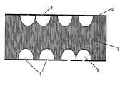
- FIG. 1is a schematic diagram of a silicon strip following surface texturing as described herein.
- FIGS. 2A-2Dare schematic diagrams illustrating a process in accordance with the present invention.
- FIG. 3is a graph showing the amount of light absorbed by strips of silicon treated by a process of the present invention (as a fraction of the amount of light entering the strip) in comparison with a silicon wafer that is polished on both sides.
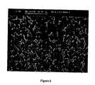
- FIGS. 4 to 6are electron micrographs of surfaces of silicon that have been textured by a process of the present invention.
- FIGS. 1 and 2 A to 2 Dare not to scale and are diagrammatic only.
- FIG. 1shows a cross sectional view of a silicon strip 1 following texturing by a process in accordance with the first embodiment of the present invention.
- the texturing processis as follows.
- a thin layer of silicon nitride 2is deposited on the silicon strip substrate 1 by low pressure chemical vapour deposition (LPCVD).
- LPCVDlow pressure chemical vapour deposition
- This techniqueresults in a uniform and conformal layer of silicon nitride 2 over the substrate surface.
- silicon nitride 2is also deposited by LPCVD down narrow channels or slots and onto the sidewalls of silicon strips created by the process described in International Patent Application No. WO 02/45143. Only a very thin layer of silicon nitride 2 , of the order of several atomic layers thick, is deposited.
- Such a layeris sufficiently thin that it contains some holes 5 through which the silicon substrate is exposed.
- Strip 1is then etched in a suitable etchant, such as a solution of 1:50 hydrofluoric:nitric acid. At room temperature, this solution etches silicon nitride about 3000 times slower than silicon. Consequently, etch pits 6 will form in the silicon of strip 1 at the position of holes 5 . After several minutes, most of the surface will be covered in etch pits 6 up to several microns in size. Etching is now terminated. Control of the etching process can be achieved by varying the silicon nitride deposition parameters, which may influence the density of holes 5 in the layer 2 , and by varying the etch time and temperature.
- a lower etch rate of silicon nitride 2 compared to silicon 1can be obtained.
- the etch solutionetches silicon nitride 2 about 6000 times slower than silicon. It is also possible to carry out the above texturing process twice in order to obtain a further improvement in the texture properties.
- FIGS. 2A-2Dshow, in diagrammatic form, cross sectional views of a silicon surface at various stages of a process according to the second embodiment of the present invention.
- a thin layer of silicon nitride 2is deposited on the surface of a silicon substrate 1 by LPCVD.
- FIG. 2Ashows the silicon substrate 1 following nitride deposition.
- Nitride layer 2as applied to the surface of silicon 1 , is not a completely smooth film but contains some thickness variations. This is shown diagrammatically in FIG. 2A by depressions 3 , 4 .
- depressionsmay extend all the way to the silicon substrate surface, creating a plurality of apertures in the nitride layer, or they may extend only part of the way through the nitride layer, as shown in FIG. 2A . Also as shown in FIG. 2A , the depressions have different depths.
- the silicon substrateis immersed in a solution which etches the silicon nitride.
- This solutioncould be, for example, a solution of 49% by weight aqueous hydrofluoric acid diluted with ten times its volume of water, or a mixture of hydrofluoric and nitric acid, such as a 1:50 by volume mixture of 49% by weight aqueous HF and 70% by weight nitric acid.
- the silicon nitride layeris gradually thinned in a uniform fashion.
- nitride layerbecomes sufficiently thin that the deepest depressions 3 expose the surface of silicon substrate 1 , creating a plurality of apertures 5 in nitride layer 2 . This is shown in FIG. 2B . Less deep depressions 4 in nitride layer 2 do not penetrate all the way through to silicon substrate 1 at this stage.
- Silicon substrate 1is now immersed in a solution which etches silicon much faster than it etches silicon nitride, such as a 1:50 by volume mixture of 49% by weight aqueous HF and 70% by weight nitric acid. This results in the formation of etch pits 6 in silicon substrate 1 at the locations where apertures 5 had been formed, as shown in FIG. 2C .
- the thin layer of silicon nitride 2 overhanging the etch pits 6is very fragile and breaks off, allowing access for fresh etchant to the etch pits 6 .
- the etch pits 6become larger as the etching process continues.
- the silicon nitride layer 2is also thinned slightly. This may result in further apertures 7 being created in it. These apertures 7 will then also lead to the formation of etch pits 8 in the silicon substrate, as is shown in FIG. 2D .
- Etchingis terminated when the optimal degree of texturing has been attained. This will be the case when most of the surface of the silicon 1 has been textured, but a small fraction of the surface is still untextured.
- Etchingcan be carried out over a range of temperatures.
- lower temperaturesgenerally lead to a lower etch rate of silicon nitride compared to the etch rate of silicon, so that etching at 0° C. rather than room temperature, for example, may be desirable in some circumstances.
- the silicon nitride layermay also be treated to decrease its etch rate in a range of silicon etchants. For example, annealing of silicon nitride at high temperatures (1000-1100° C.) generally results in a decrease in its etch rate in silicon etchants.
- the above texturing techniqueis particularly advantageous for thin film silicon cells since it only consumes a small amount of silicon in the texturing process (approximately 2-3 microns on each textured surface).
- the texturing techniquecan be applied to silicon wafers or films of arbitrary grain size.
- deposition of silicon nitridewas carried out by low pressure chemical vapour deposition at 750° C. with a dichlorosilane flowrate of 30 standard cubic centimetres per minute (sccm), an ammonia flow rate of 120 sccm and a pressure of 70 Pa. Typical deposition time was 75 seconds.
- a silicon nitride layer approximately 2 nm thickwas deposited on a polished silicon wafer of ( 111 ) orientation.
- a samplewas cut out of the wafer and etched in a solution of 1:50 hydrofluoric acid:nitric acid at 0° C.
- the samplewas encapsulated behind 1 mm thick low iron glass using silicone and its reflectance was measured using a spectrophotometer with an integrating sphere.
- the samplehad a reflectivity of 11% at 900 nm, while a polished encapsulated silicon reference wafer had a reflectivity of 24% and a sample of ( 100 ) oriented silicon textured with inverted pyramids had a reflectivity, of 8% at the same wavelength.
- a 100 mm diameter, 1 mm thick, ( 110 ) oriented silicon waferwas used. Thin silicon strips spaced 105 microns apart and approximately 70 microns thick were produced in the wafer, following the processes described in International Patent Application no. WO 02/45143. The sidewalls of the thin silicon strips so produced are highly polished. It was desired to texture the sidewalls as they would form the sunward facing surfaces in a solar cell.
- a thin layer of silicon nitridewas deposited on the wafer.
- One of the thin silicon stripswas broken out of the wafer and mounted on the wafer surface. In this way, the sidewall surface of one of the silicon strips was clearly visible during the etching process. After a period of approximately 5 minutes etching at room temperature with the same etchant described in Example 1, the strips had textured optimally and etching was terminated. The silicon strips were now approximately 65 microns thick.
- FIG. 3shows the amount of light absorbed (as a fraction of the amount of light entering the silicon) for the textured, 65 micron thick strips in comparison with untextured, 70 micron thick strips. It is clear that the texturing process results in significantly improved light trapping in the wavelength range 850-1100 nm, thus allowing significantly improved energy conversion efficiency if the texturing process is applied to silicon solar cells.
- the processes of the present inventionprovide relatively simple and inexpensive ways of reducing the reflectivity of a surface of a semiconductor material. Further, the processes of the present invention permit surfaces to be textured (and thereby have their reflectivity reduced) which are not exposed to radiation and which are therefore incapable of being textured by reactive ion etching, for example. Still further, the processes of the present invention are applicable to surfaces of ( 111 ) crystallographic orientation, which are not capable of being textured by etching with anisotropic etchants such as potassium hydroxide.
Landscapes
- Weting (AREA)
- Formation Of Insulating Films (AREA)
Abstract
Description
- The present invention relates to processes for texturing the surface of a semiconductor, and to semiconductor materials having a textured surface so as to decrease their reflectivity and/or increase the capability of the semiconductor to trap light.
- In order to maximize the efficiency of silicon solar cells, detectors or photodiodes, it is important to maximize the amount of light with a wavelength less than 1100 nm absorbed in the silicon. There are two mechanisms which can reduce the amount of light absorbed. Light may be reflected off the silicon surface, or it may enter the silicon and exit the silicon again some time later without having been absorbed. Both these loss mechanisms can be reduced by roughening, or texturing, the silicon surface. This reduces reflection losses by increasing the probability that a light ray will strike the silicon surface multiple times, and it reduces absorption losses by confining the light within the silicon (called light trapping).
- A texturing technique which can be used for single crystal silicon of (100) orientation is to etch the silicon in a solution of potassium hydroxide (KOH) and isopropyl alcohol (IPA). This results in a surface covered in square base pyramids. However, this approach cannot be used for the case where the silicon surface is not (100) crystallographic orientation. Several other texturing techniques are currently under development which do not rely on a particular crystallographic orientation, such as the use of reactive ion etching (RIE). However, these techniques may prove to be expensive or to lead to other disadvantages, such as increased carrier recombination at the silicon surface. Further, these techniques are only suitable for the texturing of flat wafers and cannot be applied, for example, to the texturing of unexposed surfaces of silicon strips which are held in a wafer frame, such as strips produced as disclosed in International Patent Application no. WO 02/45143, the disclosure of which is incorporated herein by reference in its entirety.
- Accordingly, there is a need for an improved process for decreasing the reflectivity of a surface of a semiconductor.
- It is an object of the present invention to provide such a process.
- In accordance with a first embodiment of the present invention, there is provided a process for texturing a surface of a semiconductor material, the process comprising:
- applying a layer of a protective substance on said surface wherein said layer is sufficiently thin that it has a plurality of apertures therethrough; and
- contacting said layer and said semiconductor material with an etchant capable of etching said semiconductor material faster than said protective substance, said etchant making contact with said semiconductor material at least through said apertures, for a time and under conditions in which said semiconductor material is etched by said etchant in the vicinity of said apertures to produce a textured surface on said semiconductor material, but said protective substance is substantially unetched.
- The step of applying the layer of protective substance may be a single step, or it may involve first creating a layer of protective substance that has relatively few or no apertures in it, and then partially thinning the layer of protective substance over its entire surface until it is sufficiently thin that a plurality of apertures are formed in it. The layer of protective substance, as first created, is not perfectly smooth and is therefore thinner in some places than in others. As a result, when the surface of the layer is contacted by an etchant that etches the protective substance, or is otherwise thinned, some parts of the layer will be thinned through more quickly than other parts, giving rise to a plurality of apertures in the layer.
- Accordingly, in a second embodiment of the present invention, there is provided a process for texturing a surface of a semiconductor material, the process comprising:
- creating a layer of a protective substance on said surface;
- substantially uniformly thinning said layer of protective substance until at least some apertures are formed through said layer; and
- contacting said layer and said semiconductor material with an etchant capable of etching said semiconductor material faster than said protective substance, said etchant making contact with said semiconductor material at least through said apertures, for a time and under conditions in which said semiconductor material is etched by said etchant in the vicinity of said apertures to produce a textured surface on said semiconductor material, but said protective substance is substantially unetched.
- According to a third embodiment of the present invention there is provided a semiconductor material, at least part of at least one surface of which has a plurality of pits therein wherein said pits are substantially randomly arranged over said part of said at least one surface, and have an interior surface which is at least partially rounded.
- According to a fourth embodiment of the present invention there is provided a semiconductor material, at least part of at least one surface of which has a plurality of pits therein wherein said pits are substantially randomly arranged over said part of said at least one surface, and have a width of up to 10 μm.
- According to a fifth embodiment, the invention provides a semiconductor, at least part of a surface of which has been textured by a process of the first or second embodiment.
- According to a sixth embodiment, the invention provides a semiconductor having a surface, at least part of which has been textured by etching said surface through a plurality of apertures in a layer of protective substance on said surface, said layer of protective substance having said apertures by virtue of the thinness of said layer.
- The invention further provides a semiconductor material having a layer of protective substance applied to at least part of at least one surface thereof, wherein said layer of protective substance has a plurality of apertures therethrough by virtue of the thinness of said layer.
- Semiconductor materials that have been textured by the process of the present invention are useful in the manufacture of solar cells. Accordingly, in a seventh embodiment the invention provides a solar cell comprising the semiconductor material of any of the third to sixth embodiments.
- In the processes of the present invention, by “substantially unetched” is meant that the etching is carried out under conditions in which the semiconductor material is etched in the vicinity of apertures in the protective substance, but sufficient of the protective substance remains on the surface of the semiconductor material at the end of the etching to prevent the semiconductor material from being etched in regions other than in the vicinity of the apertures.
- By “substantially uniformly” is meant that the thinning is carried out under conditions in which the protective layer is thinned at substantially the same rate over its entire surface so that, in a given time, substantially the same thickness of protective substance is removed at all points over the surface.
- In the processes of the invention, the protective substance is any substance that is resistant to etching by at least one etchant capable of etching the semiconductor material, or at least is etched by at least one etchant sufficiently more slowly than the semiconductor material is etched by that etchant so as to be substantially unetched under conditions employed in the processes of the invention.
- In the process of the first embodiment, the layer of protective substance is typically only a few atomic layers thick and may be formed by known techniques such as chemical vapour deposition or low pressure chemical vapour deposition. Other possible techniques for applying the protective substance include spray pyrolysis, evaporation, sputtering, thermal oxidation and thermal nitridation. As a further alternative, the layer of protective substance may be a layer of polymer, and is applied to the surface of the semiconductor as a layer that is sufficiently thin that it has a plurality of holes through it. In this form of the first embodiment, the etching step is suitably carried out by plasma etching. Suitably, the polymer is applied by spin coating. Examples of suitable polymers is include polymeric photoresists used in integrated circuit manufacture. Examples of suitable plasmas for etching silicon include SF6, CF4and mixtures of CF4and oxygen.
- In one form of the process of the first embodiment of the invention, the layer of protective substance is applied by low pressure chemical vapour deposition, is typically about 2 nm thick, and is an incomplete layer in that it contains numerous holes though which the semiconductor material beneath the protective layer can be etched.
- In the process of the second embodiment, the layer of protective substance may be deposited on the semiconductor material by any of the ways referred to above in reference to the process of the first embodiment. In the process of the second embodiment, the layer of protective substance, as deposited, is typically thicker than in the process of the first embodiment so that, when the layer is applied to the semiconductor, it has no apertures passing through it. However, a layer of protective substance applied to a surface is never of perfectly uniform thickness and when such a layer is gradually thinned, eventually a plurality of apertures is formed in the layer at the positions where it was thinnest prior to the etching. That is, as the layer is thinned, the thickness of the layer is decreased by substantially the same amount over its entire extent, until at least some portions of the layer are thinned through, so creating a plurality of apertures through the layer of protective substance.
- In the process of the second embodiment, the step of thinning the layer of protective substance is typically an etching step. The etchant may be any etchant capable of etching the protective substance uniformly. Such etchants are known to persons of ordinary skill in the art and include various acids and acid mixtures, and plasmas. When the protective substance is a polymer, it is preferably thinned by plasma etching, typically using an oxygen plasma.
- Typically, the apertures in the layer of protective substance are substantially randomly arranged over the surface of the protective substance, since they arise from substantially random variations in the thickness of the layer of protective substance. After the process of the first or second embodiment is carried out, therefore, etch pits remain in the semiconductor material that are substantially randomly arranged over the surface of the semiconductor material. The interior surface of the etch pits, which have the appearance of hollows formed in the surface of the semiconductor material, is usually, but not necessarily, at least partially rounded. That is, although there may be some faceting on the interior surface of the etch pits, at least part of the interior surface is usually not faceted and flat but has at least some concave regions as a result of the action of the etchant on the semiconductor material. More typically, at least half of the interior surface of the etch pits is rounded. Preferably, there is substantially no faceting on the interior surface of the etch pits. The etch pits are typically substantially circular when viewed from above the surface, except where they intersect. In some circumstances, however, the etch pits may not appear substantially circular when viewed from above, depending on the crystal orientation of the semiconductor material. Whatever their shape, the etch pits typically range in size up to about 10 μm across. More usually, the etch pits range in size from less than 1 μm to about 5 μm across. The etch pits are separated by walls that are typically thinner than the widths of the pits. Usually, at least some of the walls are substantially unetched. However, the majority of the walls are usually formed between etch pits that overlap and therefore come to a point at their top.
- The etchant in the processes of the first and second embodiments may be any etchant that is capable of etching the semiconductor material faster than the protective substance. Such etchants are known to persons of ordinary skill in the art. Where an etchant is used to thin the layer of protective substance in the process of the second embodiment, it may be the same as or different to the etchant used to etch the semiconductor. When the layer of protective substance is a polymer layer, a plasma is usually used to etch the semiconductor.
- The processes of the present invention result in a decreased reflectivity of a surface of a semiconductor material, compared to a polished surface, and/or they improve the light confinement (light trapping) within the semiconductor material.
- In the processes of the invention, the point where an optimal degree of texturing of the semiconductor surface has been reached and etching should be terminated can be determined in several ways. One way is to monitor the appearance of a surface that is being textured, such as by eye or by using an apparatus which measures the reflectance of light from the surface. A second way is to determine, for a given set of conditions (that is, the nature of the protecting substance, its thickness, the etchant composition and the temperature) the amount of time for optimal results. This can be done by etching samples for various lengths of time and then measuring the reflectance and/or light trapping behaviour of the etched samples under appropriate conditions. The results of such measurements then allow determination of the optimal etch time. It will be appreciated, however, that if an etch solution is used to texture many wafers or many batches of wafers, the etch properties of the solution will change over time. The etch time will then need to be adjusted to continue to obtain optimal texturing results.
- In the processes of the present invention, the step of contacting the semiconductor material with the etchant may result in the protective substance being etched to some extent, depending on the etchant used and the etching conditions. If the protective substance is etched to some extent during this step, this may result in more apertures being created in the protective substance, compared to the number of apertures present in the protective substance at the commencement of this step.
- Immediately before the start of the step of contacting the semiconductor material with the etchant, the apertures in the layer of protective substance are very small, typically less than 100 nm in diameter, more typically less than 10 nm in diameter. As the etching step proceeds, the apertures tend to become enlarged and their number tends to increase. At the end of this etching step, the number of apertures, and therefore the number of etch pits in the semiconductor surface, typically ranges from about 10 per 100 square microns to about 1000 per 100 square microns.
- Typically, in the processes of the first and second embodiments and in the semiconductor material of the third, fourth, fifth and sixth embodiments, the semiconductor material is silicon. When the semiconductor material is silicon, in the processes of the invention the protective substance is typically silicon nitride and the etchant is typically a mixture of hydrofluoric acid and nitric acid, such as a 1:50 by volume mixture of 49% by weight aqueous HF (that is, 49 g of HF in 100 g of aqueous solution) and 70% by weight aqueous nitric acid. Other chemicals may be added to the etchant solution to give desired etch properties, such as to improve wetting of the semiconductor surface. Such additives are well known to persons of ordinary skill in the art of semiconductor etching. When the semiconductor material is silicon, it may be single crystal silicon, microcrystalline silicon, multicrystalline silicon or polycrystalline silicon. A further possibility as an etchant for silicon nitride is a plasma of CF4and oxygen.
- The processes of the present invention typically include the further step of removing the protective substance from the surface after the step of etching the semiconductor material has proceeded sufficiently to produce a plurality of etch pits on the surface. The protective substance may be removed by applying an etchant that etches the protective substance much more rapidly than the semiconductor material. For example, when the semiconductor material is silicon and the protective substance is silicon nitride, the protective substance may be removed by reactive ion etching or by contact with phosphoric acid at elevated temperature, typically about 180° C. Alternatively, and more preferably, silicon nitride may be removed from a silicon substrate by etching in an aqueous solution of hydrogen fluoride, typically a 5% by weight solution of hydrogen fluoride in water.
- Even more typically, the processes of the present invention include the additional steps of removing the layer of protective substance after the step of etching the semiconductor material has proceeded sufficiently to produce a plurality of etch pits on the surface, and then applying an antireflective layer over the entire surface by conventional methods. It has been found that in this way, a substantially greater decrease in reflectivity is obtainable, compared to applying an antireflective coating alone.
- Typically, a process of the first embodiment or the second embodiment can give rise to a surface from which about 50% less visible light is reflected, compared to a polished surface. If an antireflective coating is applied to a surface that has been textured by a process of the present invention, an even greater decrease in the amount of visible light reflected by the surface can be achieved.
- When the semiconductor material is silicon and the layer of protective substance is a layer of silicon nitride about 2 nm thick, the step of etching the semiconductor may be achieved by contacting with a 1:50 (v/v) HF/nitric acid mixture as described above for a time of a few minutes, typically 2-5 minutes, at ordinary room temperatures.
- In some instances it may be desirable to grow a thin (for example, 20-30 nm) layer of silicon dioxide on a silicon substrate prior to silicon nitride deposition. The growth of the oxide is not necessary for carrying out the process of the present invention (it has been observed that the process of the present invention is unaffected by the presence of a layer of silicon dioxide below the silicon nitride protective substance, except for a small increase in the time taken for the process to be completed). It has been found, however, that the presence of such an oxide layer helps to avoid degradation of the electronic properties of the silicon substrate, which is sometimes observed when no oxide is present under the layer of silicon nitride.
- The process of the present invention are particularly advantageous for texturing surfaces which are not accessible to radiation, such as surfaces of silicon strips held in a frame of silicon and produced as described in International Patent Application No. WO 02/45143. Thus, in one preferred form of the invention, the semiconductor material is a strip of silicon having a thickness of less than 100 μm and a width of up to about 3 nmm and wherein at least one opposite pair of surfaces has been textured by a process according to the present invention. That is, each of at least one pair of opposite surfaces has a plurality of pits therein wherein the pits are substantially randomly distributed over the surface of the strip, and have an interior surface which is at least partially rounded, and/or have a width of up to 10 μm.
- Preferred embodiments of the present invention are hereinafter described, by way of example only, with reference to the accompanying drawings, which are briefly described as follows.
FIG. 1 is a schematic diagram of a silicon strip following surface texturing as described herein.FIGS. 2A-2D are schematic diagrams illustrating a process in accordance with the present invention.FIG. 3 is a graph showing the amount of light absorbed by strips of silicon treated by a process of the present invention (as a fraction of the amount of light entering the strip) in comparison with a silicon wafer that is polished on both sides.- FIGS.4 to6 are electron micrographs of surfaces of silicon that have been textured by a process of the present invention.
- The accompanying Figures are provided to facilitate an understanding of the invention. It will be appreciated that
FIGS. 1 and 2 A to2D are not to scale and are diagrammatic only. FIG. 1 shows a cross sectional view of asilicon strip 1 following texturing by a process in accordance with the first embodiment of the present invention. The texturing process is as follows. A thin layer ofsilicon nitride 2 is deposited on thesilicon strip substrate 1 by low pressure chemical vapour deposition (LPCVD). This technique results in a uniform and conformal layer ofsilicon nitride 2 over the substrate surface. Importantly,silicon nitride 2 is also deposited by LPCVD down narrow channels or slots and onto the sidewalls of silicon strips created by the process described in International Patent Application No. WO 02/45143. Only a very thin layer ofsilicon nitride 2, of the order of several atomic layers thick, is deposited. Such a layer is sufficiently thin that it contains someholes 5 through which the silicon substrate is exposed.Strip 1 is then etched in a suitable etchant, such as a solution of 1:50 hydrofluoric:nitric acid. At room temperature, this solution etches silicon nitride about 3000 times slower than silicon. Consequently, etch pits6 will form in the silicon ofstrip 1 at the position ofholes 5. After several minutes, most of the surface will be covered inetch pits 6 up to several microns in size. Etching is now terminated. Control of the etching process can be achieved by varying the silicon nitride deposition parameters, which may influence the density ofholes 5 in thelayer 2, and by varying the etch time and temperature. If a lower etch temperature is used, a lower etch rate ofsilicon nitride 2 compared tosilicon 1 can be obtained. For example, at 0° C., the etch solution etchessilicon nitride 2 about 6000 times slower than silicon. It is also possible to carry out the above texturing process twice in order to obtain a further improvement in the texture properties.FIGS. 2A-2D show, in diagrammatic form, cross sectional views of a silicon surface at various stages of a process according to the second embodiment of the present invention. A thin layer ofsilicon nitride 2, of the order of 2-4 nm thick, is deposited on the surface of asilicon substrate 1 by LPCVD.FIG. 2A shows thesilicon substrate 1 following nitride deposition.Nitride layer 2, as applied to the surface ofsilicon 1, is not a completely smooth film but contains some thickness variations. This is shown diagrammatically inFIG. 2A bydepressions 3,4. Depending on the thickness of the applied nitride layer, depressions may extend all the way to the silicon substrate surface, creating a plurality of apertures in the nitride layer, or they may extend only part of the way through the nitride layer, as shown inFIG. 2A . Also as shown inFIG. 2A , the depressions have different depths.- In the case where the depressions in the nitride layer do not extend all the way through the nitride layer, the silicon substrate is immersed in a solution which etches the silicon nitride. This solution could be, for example, a solution of 49% by weight aqueous hydrofluoric acid diluted with ten times its volume of water, or a mixture of hydrofluoric and nitric acid, such as a 1:50 by volume mixture of 49% by weight aqueous HF and 70% by weight nitric acid. The silicon nitride layer is gradually thinned in a uniform fashion. Eventually the nitride layer becomes sufficiently thin that the
deepest depressions 3 expose the surface ofsilicon substrate 1, creating a plurality ofapertures 5 innitride layer 2. This is shown inFIG. 2B . Less deep depressions4 innitride layer 2 do not penetrate all the way through tosilicon substrate 1 at this stage. Silicon substrate 1 is now immersed in a solution which etches silicon much faster than it etches silicon nitride, such as a 1:50 by volume mixture of 49% by weight aqueous HF and 70% by weight nitric acid. This results in the formation ofetch pits 6 insilicon substrate 1 at the locations whereapertures 5 had been formed, as shown inFIG. 2C . The thin layer ofsilicon nitride 2 overhanging the etch pits6 is very fragile and breaks off, allowing access for fresh etchant to the etch pits6. The etch pits6 become larger as the etching process continues.- As the etching proceeds, the
silicon nitride layer 2 is also thinned slightly. This may result infurther apertures 7 being created in it. Theseapertures 7 will then also lead to the formation ofetch pits 8 in the silicon substrate, as is shown inFIG. 2D . Etching is terminated when the optimal degree of texturing has been attained. This will be the case when most of the surface of thesilicon 1 has been textured, but a small fraction of the surface is still untextured. - Etching can be carried out over a range of temperatures. In particular, lower temperatures generally lead to a lower etch rate of silicon nitride compared to the etch rate of silicon, so that etching at 0° C. rather than room temperature, for example, may be desirable in some circumstances. The silicon nitride layer may also be treated to decrease its etch rate in a range of silicon etchants. For example, annealing of silicon nitride at high temperatures (1000-1100° C.) generally results in a decrease in its etch rate in silicon etchants.
- The above texturing technique is particularly advantageous for thin film silicon cells since it only consumes a small amount of silicon in the texturing process (approximately 2-3 microns on each textured surface). The texturing technique can be applied to silicon wafers or films of arbitrary grain size.
- In all of the following examples, deposition of silicon nitride was carried out by low pressure chemical vapour deposition at 750° C. with a dichlorosilane flowrate of 30 standard cubic centimetres per minute (sccm), an ammonia flow rate of 120 sccm and a pressure of 70 Pa. Typical deposition time was 75 seconds.
- A silicon nitride layer approximately 2 nm thick was deposited on a polished silicon wafer of (111) orientation. A sample was cut out of the wafer and etched in a solution of 1:50 hydrofluoric acid:nitric acid at 0° C. The sample was encapsulated behind 1 mm thick low iron glass using silicone and its reflectance was measured using a spectrophotometer with an integrating sphere. The sample had a reflectivity of 11% at 900 nm, while a polished encapsulated silicon reference wafer had a reflectivity of 24% and a sample of (100) oriented silicon textured with inverted pyramids had a reflectivity, of 8% at the same wavelength. These results indicate that the texturing process is very effective at reducing reflection from the silicon surface.
- A 100 mm diameter, 1 mm thick, (110) oriented silicon wafer was used. Thin silicon strips spaced 105 microns apart and approximately 70 microns thick were produced in the wafer, following the processes described in International Patent Application no. WO 02/45143. The sidewalls of the thin silicon strips so produced are highly polished. It was desired to texture the sidewalls as they would form the sunward facing surfaces in a solar cell.
- A thin layer of silicon nitride was deposited on the wafer. One of the thin silicon strips was broken out of the wafer and mounted on the wafer surface. In this way, the sidewall surface of one of the silicon strips was clearly visible during the etching process. After a period of approximately 5 minutes etching at room temperature with the same etchant described in Example 1, the strips had textured optimally and etching was terminated. The silicon strips were now approximately 65 microns thick.
- Measurements were carried out to determine the degree of light confinement (light trapping) within the textured silicon.
FIG. 3 shows the amount of light absorbed (as a fraction of the amount of light entering the silicon) for the textured, 65 micron thick strips in comparison with untextured, 70 micron thick strips. It is clear that the texturing process results in significantly improved light trapping in the wavelength range 850-1100 nm, thus allowing significantly improved energy conversion efficiency if the texturing process is applied to silicon solar cells. - Several (111) oriented, >1000 ohm-cm, boron doped float-zoned silicon wafers were used. An oxide approximately 30 nm thick was thermally grown on the wafers. A thin layer of silicon nitride was then deposited and the wafers were textured as described in Example 2. Following texturing, the wafers were given a phosphorus diffusion and a 30 nm thick oxide was thermally grown. The wafers were then given an anneal in a mixture of 5% hydrogen and 95% nitrogen at 430° C. for 30 minutes. The emitter saturation current density following these treatments was measured to be 20-25 fA/cm2per side. This low value indicates that excellent surface passivation can be achieved on the textured surfaces.
- ADVANTAGES OF THE PROCESSES OF THE PRESENT INVENTION
- The processes of the present invention provide relatively simple and inexpensive ways of reducing the reflectivity of a surface of a semiconductor material. Further, the processes of the present invention permit surfaces to be textured (and thereby have their reflectivity reduced) which are not exposed to radiation and which are therefore incapable of being textured by reactive ion etching, for example. Still further, the processes of the present invention are applicable to surfaces of (111) crystallographic orientation, which are not capable of being textured by etching with anisotropic etchants such as potassium hydroxide.
- Many modifications of the processes described herein with reference to the accompanying drawings and Examples will be apparent to those skilled in the art without departing from the scope of the present invention.
Claims (23)
Applications Claiming Priority (3)
| Application Number | Priority Date | Filing Date | Title |
|---|---|---|---|
| WOPCT/AU01/01546 | 2001-11-29 | ||
| PCT/AU2001/001546WO2002045143A1 (en) | 2000-11-29 | 2001-11-29 | Semiconductor wafer processing to increase the usable planar surface area |
| PCT/AU2002/001625WO2003047004A1 (en) | 2001-11-29 | 2002-11-29 | Semiconductor texturing process |
Publications (2)
| Publication Number | Publication Date |
|---|---|
| US20050104163A1true US20050104163A1 (en) | 2005-05-19 |
| US7828983B2 US7828983B2 (en) | 2010-11-09 |
Family
ID=3700898
Family Applications (1)
| Application Number | Title | Priority Date | Filing Date |
|---|---|---|---|
| US10/497,248Expired - Fee RelatedUS7828983B2 (en) | 2001-11-29 | 2002-11-29 | Semiconductor texturing process |
Country Status (10)
| Country | Link |
|---|---|
| US (1) | US7828983B2 (en) |
| EP (1) | EP1461834A4 (en) |
| JP (1) | JP4530662B2 (en) |
| KR (1) | KR20040068928A (en) |
| CN (1) | CN1613155B (en) |
| CA (1) | CA2467112C (en) |
| IL (1) | IL162190A0 (en) |
| MY (1) | MY144264A (en) |
| WO (1) | WO2003047004A1 (en) |
| ZA (1) | ZA200405144B (en) |
Cited By (10)
| Publication number | Priority date | Publication date | Assignee | Title |
|---|---|---|---|---|
| US20040097012A1 (en)* | 2000-11-29 | 2004-05-20 | Weber Klaus Johannes | Semiconductor wafer processing to increase the usable planar surface area |
| US20070105266A1 (en)* | 2005-11-10 | 2007-05-10 | Tatung Company | Anti-reflective substrate and the manufacturing method thereof |
| US20110041910A1 (en)* | 2009-08-18 | 2011-02-24 | Semiconductor Energy Laboratory Co., Ltd. | Photoelectric conversion device and manufacturing method thereof |
| US20110204489A1 (en)* | 2010-02-25 | 2011-08-25 | National Taiwan University | Silicon substrate having nanostructures and method for producing the same and application thereof |
| US20110212622A1 (en)* | 2010-02-26 | 2011-09-01 | International Business Machines Corporation | Surface texturing using a low quality dielectric layer |
| US20140110805A1 (en)* | 2012-10-18 | 2014-04-24 | Infineon Technologies Dresden Gmbh | Silicon light trap devices, systems and methods |
| US8957490B2 (en) | 2013-06-28 | 2015-02-17 | Infineon Technologies Dresden Gmbh | Silicon light trap devices |
| CN106206785A (en)* | 2015-04-09 | 2016-12-07 | 新日光能源科技股份有限公司 | Solar cell and manufacturing method thereof |
| US20200220033A1 (en)* | 2013-09-10 | 2020-07-09 | Advanced Silicon Group, Inc. | Metal-assisted etch combined with regularizing etch |
| CN114078894A (en)* | 2020-08-13 | 2022-02-22 | 豪威科技股份有限公司 | Cell Deep Trench Isolation Pyramid Structure for CMOS Image Sensors |
Families Citing this family (33)
| Publication number | Priority date | Publication date | Assignee | Title |
|---|---|---|---|---|
| US7442629B2 (en) | 2004-09-24 | 2008-10-28 | President & Fellows Of Harvard College | Femtosecond laser-induced formation of submicrometer spikes on a semiconductor substrate |
| US7057256B2 (en) | 2001-05-25 | 2006-06-06 | President & Fellows Of Harvard College | Silicon-based visible and near-infrared optoelectric devices |
| US7910822B1 (en) | 2005-10-17 | 2011-03-22 | Solaria Corporation | Fabrication process for photovoltaic cell |
| US8227688B1 (en) | 2005-10-17 | 2012-07-24 | Solaria Corporation | Method and resulting structure for assembling photovoltaic regions onto lead frame members for integration on concentrating elements for solar cells |
| USD555083S1 (en) | 2005-11-08 | 2007-11-13 | Solaria Corporation | Solar cell package design |
| USD558139S1 (en) | 2005-11-18 | 2007-12-25 | Solaria Corporation | Triangular solar cell design |
| USD555084S1 (en) | 2005-11-18 | 2007-11-13 | Solaria Corporation | Circular solar cell package design |
| USD559174S1 (en) | 2005-11-18 | 2008-01-08 | Solaria Corporation | Shaped solar cell package design |
| USD568238S1 (en) | 2005-11-18 | 2008-05-06 | Solaria Corporation | Rectangular solar cell package design |
| EP1965439A3 (en)* | 2007-02-28 | 2010-03-24 | Centrotherm Photovoltaics Technology GmbH | Method for texturising surfaces |
| US7910392B2 (en) | 2007-04-02 | 2011-03-22 | Solaria Corporation | Method and system for assembling a solar cell package |
| USD588534S1 (en) | 2007-07-26 | 2009-03-17 | Solaria Corporation | Shaped solar cell package |
| US8049098B2 (en) | 2007-09-05 | 2011-11-01 | Solaria Corporation | Notch structure for concentrating module and method of manufacture using photovoltaic strips |
| US7910035B2 (en) | 2007-12-12 | 2011-03-22 | Solaria Corporation | Method and system for manufacturing integrated molded concentrator photovoltaic device |
| USD591229S1 (en) | 2008-01-24 | 2009-04-28 | Solaria Corporation | Shaped solar cell package |
| US9673243B2 (en) | 2009-09-17 | 2017-06-06 | Sionyx, Llc | Photosensitive imaging devices and associated methods |
| US9911781B2 (en) | 2009-09-17 | 2018-03-06 | Sionyx, Llc | Photosensitive imaging devices and associated methods |
| US8692198B2 (en) | 2010-04-21 | 2014-04-08 | Sionyx, Inc. | Photosensitive imaging devices and associated methods |
| WO2011160130A2 (en) | 2010-06-18 | 2011-12-22 | Sionyx, Inc | High speed photosensitive devices and associated methods |
| CN102097534A (en)* | 2010-11-18 | 2011-06-15 | 中国科学院宁波材料技术与工程研究所 | Method for simultaneously forming crystal silicon solar cell PN junction and silicon nitride antireflection film |
| US8440494B2 (en) | 2011-05-20 | 2013-05-14 | International Business Machines Corporation | Single-crystalline silicon alkaline texturing with glycerol or ethylene glycol additives |
| USD699176S1 (en) | 2011-06-02 | 2014-02-11 | Solaria Corporation | Fastener for solar modules |
| US9496308B2 (en) | 2011-06-09 | 2016-11-15 | Sionyx, Llc | Process module for increasing the response of backside illuminated photosensitive imagers and associated methods |
| US8637405B2 (en) | 2011-06-21 | 2014-01-28 | International Business Machines Corporation | Silicon surface texturing method for reducing surface reflectance |
| WO2013010127A2 (en) | 2011-07-13 | 2013-01-17 | Sionyx, Inc. | Biometric imaging devices and associated methods |
| US9064764B2 (en) | 2012-03-22 | 2015-06-23 | Sionyx, Inc. | Pixel isolation elements, devices, and associated methods |
| US10872988B1 (en) | 2013-02-03 | 2020-12-22 | Mark R. Schroeder | Photovoltaic device |
| US11538949B2 (en) | 2013-02-03 | 2022-12-27 | Mark R. Schroeder | Sensor comprising a photovoltaic device |
| US9762830B2 (en) | 2013-02-15 | 2017-09-12 | Sionyx, Llc | High dynamic range CMOS image sensor having anti-blooming properties and associated methods |
| WO2014151093A1 (en) | 2013-03-15 | 2014-09-25 | Sionyx, Inc. | Three dimensional imaging utilizing stacked imager devices and associated methods |
| US9209345B2 (en) | 2013-06-29 | 2015-12-08 | Sionyx, Inc. | Shallow trench textured regions and associated methods |
| US8951825B1 (en) | 2013-09-10 | 2015-02-10 | Palo Alto Research Center Incorporated | Solar cell texturing |
| DE102020111371A1 (en)* | 2020-02-27 | 2021-09-02 | Taiwan Semiconductor Manufacturing Co. Ltd. | ABSORPTION ENRICHMENT STRUCTURE TO INCREASE THE QUANTUM EFFICIENCY OF AN IMAGE SENSOR |
Citations (99)
| Publication number | Priority date | Publication date | Assignee | Title |
|---|---|---|---|---|
| US3278811A (en)* | 1960-10-04 | 1966-10-11 | Hayakawa Denki Kogyo Kabushiki | Radiation energy transducing device |
| US3422527A (en)* | 1965-06-21 | 1969-01-21 | Int Rectifier Corp | Method of manufacture of high voltage solar cell |
| US3647581A (en)* | 1968-07-11 | 1972-03-07 | Itt | Manufacture of semiconductor devices |
| US3690953A (en)* | 1970-09-10 | 1972-09-12 | Us Air Force | Vertical junction hardened solar cell |
| US3985579A (en)* | 1975-11-26 | 1976-10-12 | The United States Of America As Represented By The Secretary Of The Air Force | Rib and channel vertical multijunction solar cell |
| US4038104A (en)* | 1976-06-07 | 1977-07-26 | Kabushiki Kaisha Suwa Seikosha | Solar battery |
| US4082570A (en)* | 1976-02-09 | 1978-04-04 | Semicon, Inc. | High intensity solar energy converter |
| US4110122A (en)* | 1976-05-26 | 1978-08-29 | Massachusetts Institute Of Technology | High-intensity, solid-state-solar cell device |
| US4153476A (en)* | 1978-03-29 | 1979-05-08 | Nasa | Double-sided solar cell package |
| US4278473A (en)* | 1979-08-24 | 1981-07-14 | Varian Associates, Inc. | Monolithic series-connected solar cell |
| US4332973A (en)* | 1974-11-08 | 1982-06-01 | Sater Bernard L | High intensity solar cell |
| US4406913A (en)* | 1980-12-16 | 1983-09-27 | Siemens Aktiengesellschaft | Solar cell with increased efficiency |
| US4409423A (en)* | 1982-03-09 | 1983-10-11 | The United States Of America As Represented By The Secretary Of The Air Force | Hole matrix vertical junction solar cell |
| US4409422A (en)* | 1974-11-08 | 1983-10-11 | Sater Bernard L | High intensity solar cell |
| US4444992A (en)* | 1980-11-12 | 1984-04-24 | Massachusetts Institute Of Technology | Photovoltaic-thermal collectors |
| US4516314A (en)* | 1974-11-08 | 1985-05-14 | Sater Bernard L | Method of making a high intensity solar cell |
| US4527183A (en)* | 1981-07-10 | 1985-07-02 | General Electric Company | Drilled, diffused radiation detector |
| US4554727A (en)* | 1982-08-04 | 1985-11-26 | Exxon Research & Engineering Company | Method for making optically enhanced thin film photovoltaic device using lithography defined random surfaces |
| US4686321A (en)* | 1985-07-02 | 1987-08-11 | Sanyo Electric Co., Ltd. | Photovoltaic device and method of manufacturing thereof |
| US4692782A (en)* | 1983-06-08 | 1987-09-08 | Fuji Electric Corporate Research & Development Co., Ltd. | Semiconductor radioactive ray detector |
| US4805006A (en)* | 1987-03-25 | 1989-02-14 | Matsushita Electric Works, Ltd. | Light receiving element |
| US4883561A (en)* | 1988-03-29 | 1989-11-28 | Bell Communications Research, Inc. | Lift-off and subsequent bonding of epitaxial films |
| US4892592A (en)* | 1987-03-26 | 1990-01-09 | Solarex Corporation | Thin film semiconductor solar cell array and method of making |
| US4982099A (en)* | 1985-02-12 | 1991-01-01 | Siemens Aktiengesellschaft | Aperture diaphragm for a lithography apparatus |
| US4989059A (en)* | 1988-05-13 | 1991-01-29 | Mobil Solar Energy Corporation | Solar cell with trench through pn junction |
| US5011544A (en)* | 1989-09-08 | 1991-04-30 | Solarex Corporation | Solar panel with interconnects and masking structure, and method |
| US5016073A (en)* | 1984-07-06 | 1991-05-14 | The Secretary Of State For Defence In Her Britannic Majesty's Government Of The United Kingdom Of Great Britain And Northern Ireland | Photodetector semiconductor which does not require extensive cooling |
| US5067985A (en)* | 1990-06-08 | 1991-11-26 | The United States Of America As Represented By The Secretary Of The Air Force | Back-contact vertical-junction solar cell and method |
| US5081409A (en)* | 1989-11-13 | 1992-01-14 | Performance Controls, Inc. | Pulse-width modulated circuit for driving a load |
| US5082791A (en)* | 1988-05-13 | 1992-01-21 | Mobil Solar Energy Corporation | Method of fabricating solar cells |
| US5098482A (en)* | 1990-11-07 | 1992-03-24 | Solarex Corporation | Vertical junction solar cell |
| US5116464A (en)* | 1989-06-02 | 1992-05-26 | Massachusetts Institute Of Technology | Cesium hydroxide etch of a semiconductor crystal |
| US5136346A (en)* | 1990-09-07 | 1992-08-04 | Motorola, Inc. | Photon stimulated variable capacitance effect devices |
| US5139974A (en)* | 1991-01-25 | 1992-08-18 | Micron Technology, Inc. | Semiconductor manufacturing process for decreasing the optical refelctivity of a metal layer |
| US5149676A (en)* | 1990-06-22 | 1992-09-22 | Hyundai Electronics Industries Co., Ltd. | Silicon layer having increased surface area and method for manufacturing |
| US5266125A (en)* | 1992-05-12 | 1993-11-30 | Astropower, Inc. | Interconnected silicon film solar cell array |
| US5279703A (en)* | 1990-07-06 | 1994-01-18 | Fraunhofer Gesellschaft Zur Forderung Der Angewandten Forschung E.V. | Process for the thin etching of substrates |
| US5306647A (en)* | 1992-01-29 | 1994-04-26 | Siemens Aktiengesellschaft | Method for manufacturing a solar cell from a substrate wafer |
| US5324679A (en)* | 1991-03-23 | 1994-06-28 | Samsung Electronics Co., Ltd. | Method for manufacturing a semiconductor device having increased surface area conductive layer |
| US5330584A (en)* | 1991-10-17 | 1994-07-19 | Sharp Kabushiki Kaisha | Solar cell |
| US5344517A (en)* | 1993-04-22 | 1994-09-06 | Bandgap Technology Corporation | Method for lift-off of epitaxial layers and applications thereof |
| US5352530A (en)* | 1985-12-23 | 1994-10-04 | Bridgestone Corporation | Transparent films and laminates having the same |
| US5367217A (en)* | 1992-11-18 | 1994-11-22 | Alliedsignal Inc. | Four bar resonating force transducer |
| US5389158A (en)* | 1989-04-17 | 1995-02-14 | The Boeing Company | Low bandgap photovoltaic cell with inherent bypass diode |
| US5391236A (en)* | 1993-07-30 | 1995-02-21 | Spectrolab, Inc. | Photovoltaic microarray structure and fabrication method |
| US5447576A (en)* | 1992-08-03 | 1995-09-05 | Siemens Solar Industries International, Inc. | Composition and method for encapsulating a solar cell which minimizes thermal discoloration |
| US5461002A (en)* | 1990-05-30 | 1995-10-24 | Safir; Yakov | Method of making diffused doped areas for semiconductor components |
| US5466302A (en)* | 1994-05-09 | 1995-11-14 | Regents Of The University Of California | Solar cell array interconnects |
| US5470761A (en)* | 1993-09-13 | 1995-11-28 | Westinghouse Electric Corporation | Process for fabricating a front surface resonant mesh array detector |
| US5494832A (en)* | 1993-03-29 | 1996-02-27 | Siemens Aktiengesellschaft | Method for manufacturing a solar cell from a substrate wafer |
| US5538563A (en)* | 1995-02-03 | 1996-07-23 | Finkl; Anthony W. | Solar energy concentrator apparatus for bifacial photovoltaic cells |
| US5538902A (en)* | 1993-06-29 | 1996-07-23 | Sanyo Electric Co., Ltd. | Method of fabricating a photovoltaic device having a three-dimensional shape |
| US5567248A (en)* | 1995-09-05 | 1996-10-22 | Chung; Darius | Modular solar cell contact arrangement |
| US5567656A (en)* | 1993-12-27 | 1996-10-22 | Goldstar Electron Co., Ltd. | Process for packaging semiconductor device |
| US5609694A (en)* | 1994-04-28 | 1997-03-11 | Sharp Kabushiki Kaisha | Solar cell and a method of manufacturing thereof |
| US5641381A (en)* | 1995-03-27 | 1997-06-24 | The United States Of America As Represented By The Administrator Of The National Aeronautics And Space Administration | Preferentially etched epitaxial liftoff of InP material |
| US5733382A (en)* | 1995-12-18 | 1998-03-31 | Hanoka; Jack I. | Solar cell modules and method of making same |
| US5773791A (en)* | 1996-09-03 | 1998-06-30 | Kuykendal; Robert | Water laser machine tool |
| US5895530A (en)* | 1996-02-26 | 1999-04-20 | Applied Materials, Inc. | Method and apparatus for directing fluid through a semiconductor processing chamber |
| US5902120A (en)* | 1997-03-13 | 1999-05-11 | Micronas Intermetall Gmbh | Process for producing spatially patterned components |
| US5904548A (en)* | 1996-11-21 | 1999-05-18 | Texas Instruments Incorporated | Trench scribe line for decreased chip spacing |
| US5904546A (en)* | 1996-02-12 | 1999-05-18 | Micron Technology, Inc. | Method and apparatus for dicing semiconductor wafers |
| US5930644A (en)* | 1997-07-23 | 1999-07-27 | Taiwan Semiconductor Manufacturing Co., Ltd. | Method of forming a shallow trench isolation using oxide slope etching |
| US5972732A (en)* | 1997-12-19 | 1999-10-26 | Sandia Corporation | Method of monolithic module assembly |
| US5985742A (en)* | 1997-05-12 | 1999-11-16 | Silicon Genesis Corporation | Controlled cleavage process and device for patterned films |
| US5994641A (en)* | 1998-04-24 | 1999-11-30 | Ase Americas, Inc. | Solar module having reflector between cells |
| US6066516A (en)* | 1995-06-26 | 2000-05-23 | Seiko Epson Corporation | Method for forming crystalline semiconductor layers, a method for fabricating thin film transistors, and method for fabricating solar cells and active matrix liquid crystal devices |
| US6074514A (en)* | 1998-02-09 | 2000-06-13 | Applied Materials, Inc. | High selectivity etch using an external plasma discharge |
| US6091021A (en)* | 1996-11-01 | 2000-07-18 | Sandia Corporation | Silicon cells made by self-aligned selective-emitter plasma-etchback process |
| US6107161A (en)* | 1996-06-07 | 2000-08-22 | Rohm Co., Ltd. | Semiconductor chip and a method for manufacturing thereof |
| US6110793A (en)* | 1998-06-24 | 2000-08-29 | Taiwan Semiconductor Manufacturing Company | Method for making a trench isolation having a conformal liner oxide and top and bottom rounded corners for integrated circuits |
| US6127623A (en)* | 1998-07-03 | 2000-10-03 | Sharp Kabushiki Kaisha | Solar cell and production process therefor |
| US6126311A (en)* | 1998-11-02 | 2000-10-03 | Claud S. Gordon Company | Dew point sensor using mems |
| US6127714A (en)* | 1997-10-01 | 2000-10-03 | Canon Kabushiki Kaisha | Method for producing semiconductor device and photodetector device |
| US6130380A (en)* | 1997-04-28 | 2000-10-10 | Sharp Kabushiki Kaisha | Solar cell and fabrication method thereof |
| US6140603A (en)* | 1999-03-31 | 2000-10-31 | Taiwan Semiconductor Manufacturing Co., Ltd | Micro-cleavage method for specimen preparation |
| US6168968B1 (en)* | 1997-02-27 | 2001-01-02 | Sharp Kabushiki Kaisha | Method of fabricating integrated thin film solar cells |
| US6172297B1 (en)* | 1997-09-23 | 2001-01-09 | Institut Fur Solarenergieforschung Gmbh | Solar cell and method for fabrication of a solar cell |
| US6180869B1 (en)* | 1997-05-06 | 2001-01-30 | Ebara Solar, Inc. | Method and apparatus for self-doping negative and positive electrodes for silicon solar cells and other devices |
| US6184457B1 (en)* | 1997-12-22 | 2001-02-06 | Canon Kabushiki Kaisha | Photovoltaic device module |
| US6262358B1 (en)* | 1999-02-18 | 2001-07-17 | Sharp Kabushiki Kaisha | Solar cell module and solar cell panel using the same |
| US6265653B1 (en)* | 1998-12-10 | 2001-07-24 | The Regents Of The University Of California | High voltage photovoltaic power converter |
| US6265741B1 (en)* | 1998-04-06 | 2001-07-24 | Siemens Aktiengesellschaft | Trench capacitor with epi buried layer |
| US20010013630A1 (en)* | 2000-01-13 | 2001-08-16 | Chromux Technologies, Inc. | Isolation in micromachined single crystal silicon using deep trench insulation |
| US6294723B2 (en)* | 1998-02-26 | 2001-09-25 | Hitachi, Ltd. | Photovoltaic device, photovoltaic module and establishing method of photovoltaic system |
| US6406979B2 (en)* | 2000-06-27 | 2002-06-18 | Robert Bosch Gmbh | Method for sectioning a substrate wafer into a plurality of substrate chips |
| US6407327B1 (en)* | 1998-06-04 | 2002-06-18 | Tecstar Power Systems, Inc. | Modular, glass covered solar cell array |
| US6407329B1 (en)* | 1999-04-07 | 2002-06-18 | Bridgestone Corporation | Backside covering member for solar battery, sealing film and solar battery |
| US6410843B1 (en)* | 1999-11-22 | 2002-06-25 | Sanyo Electric Co., Ltd. | Solar cell module |
| US20020119290A1 (en)* | 2001-01-03 | 2002-08-29 | Sang-Wook Park | Textured semiconductor wafer for solar cell |
| US6455873B1 (en)* | 1997-12-03 | 2002-09-24 | State Of Oregon Acting By And Through The State Board Of Higher Education On Behalf Of The University Of Oregon | Devices having a semiconductor/conducting polymer interface |
| US6515218B1 (en)* | 1999-11-22 | 2003-02-04 | Canon Kabushiki Kaisha | Photovoltaic element, process for the production thereof, method for removing a cover portion of a covered wire, and method for joining a covered wire and a conductor |
| US6515217B1 (en)* | 2001-09-11 | 2003-02-04 | Eric Aylaian | Solar cell having a three-dimensional array of photovoltaic cells enclosed within an enclosure having reflective surfaces |
| US6525374B1 (en)* | 1998-10-29 | 2003-02-25 | Infineon Technologies Ag | Semiconductor component with a high breakdown voltage |
| US6553729B1 (en)* | 2000-06-09 | 2003-04-29 | United Solar Systems Corporation | Self-adhesive photovoltaic module |
| US6583032B1 (en)* | 1999-11-05 | 2003-06-24 | Tokyo Seimitsu Co., Ltd. | Method for manufacturing semiconductor chips |
| US20040097012A1 (en)* | 2000-11-29 | 2004-05-20 | Weber Klaus Johannes | Semiconductor wafer processing to increase the usable planar surface area |
| US20040119067A1 (en)* | 2000-12-14 | 2004-06-24 | Nitronex Corporation | Gallium nitride materials and methods |
| US6846984B2 (en)* | 2000-04-27 | 2005-01-25 | Universitat Konstanz | Solar cell and method for making a solar cell |
Family Cites Families (53)
| Publication number | Priority date | Publication date | Assignee | Title |
|---|---|---|---|---|
| JPS495265A (en) | 1972-04-28 | 1974-01-17 | ||
| JPS5373075A (en)* | 1976-12-13 | 1978-06-29 | Fujitsu Ltd | Treatment method for wafer surface |
| US4407695A (en)* | 1981-12-31 | 1983-10-04 | Exxon Research And Engineering Co. | Natural lithographic fabrication of microstructures over large areas |
| US4633031A (en) | 1982-09-24 | 1986-12-30 | Todorof William J | Multi-layer thin film, flexible silicon alloy photovoltaic cell |
| JPS5959883A (en)* | 1982-09-30 | 1984-04-05 | Fujitsu Ltd | Surface roughening method |
| JPS59123279A (en)* | 1982-12-28 | 1984-07-17 | Semiconductor Energy Lab Co Ltd | Manufacture of photoelectric conversion device |
| JPS59123283A (en)* | 1982-12-28 | 1984-07-17 | Semiconductor Energy Lab Co Ltd | Photoelectric conversion device |
| JPS59123279U (en) | 1983-02-09 | 1984-08-20 | オリオン機械株式会社 | Defrosting device for gas cooling equipment |
| US4626613A (en) | 1983-12-23 | 1986-12-02 | Unisearch Limited | Laser grooved solar cell |
| JPS61108176A (en)* | 1984-11-01 | 1986-05-26 | Fuji Electric Co Ltd | Roughening method |
| JPS61108176U (en) | 1984-12-19 | 1986-07-09 | ||
| JPS6254927A (en)* | 1985-09-03 | 1987-03-10 | Sanyo Electric Co Ltd | Photovoltaic device |
| DE3803769A1 (en) | 1988-02-08 | 1989-08-17 | Siemens Ag | METHOD FOR THE PRODUCTION OF THICK, RIBBON-SHAPED SILICON CRYSTALS WITH LEVEL SURFACE, SUITABLE FOR THE SOLAR CELL PRODUCTION |
| US5081049A (en) | 1988-07-18 | 1992-01-14 | Unisearch Limited | Sculpted solar cell surfaces |
| US5073230A (en) | 1990-04-17 | 1991-12-17 | Arizona Board Of Regents Acting On Behalf Of Arizona State University | Means and methods of lifting and relocating an epitaxial device layer |
| JP3276682B2 (en) | 1992-08-06 | 2002-04-22 | オリンパス光学工業株式会社 | Endoscope bending operation device |
| JPH06213554A (en) | 1993-01-14 | 1994-08-02 | Fuji Electric Co Ltd | Cold air circulation open showcase |
| JPH07188947A (en)* | 1993-12-27 | 1995-07-25 | Sumitomo Metal Mining Co Ltd | Surface roughening method |
| US5478402A (en) | 1994-02-17 | 1995-12-26 | Ase Americas, Inc. | Solar cell modules and method of making same |
| US5474620A (en) | 1994-05-16 | 1995-12-12 | United Solar Systems Corporation | Cut resistant laminate for the light incident surface of a photovoltaic module |
| EP0718873A3 (en) | 1994-12-21 | 1998-04-15 | MEMC Electronic Materials, Inc. | Cleaning process for hydrophobic silicon wafers |
| JPH08213554A (en)* | 1995-02-02 | 1996-08-20 | Miyazaki Oki Electric Co Ltd | Forming method of roughened polysilicon film |
| EP0771475B1 (en) | 1995-05-19 | 2005-12-21 | Dr. Johannes Heidenhain GmbH | Radiation-sensitive detector element |
| JP2915327B2 (en) | 1995-07-19 | 1999-07-05 | キヤノン株式会社 | Solar cell module and method of manufacturing the same |
| US5851928A (en)* | 1995-11-27 | 1998-12-22 | Motorola, Inc. | Method of etching a semiconductor substrate |
| US5841179A (en) | 1996-08-28 | 1998-11-24 | Advanced Micro Devices, Inc. | Conductive layer with anti-reflective surface portion |
| US6162658A (en) | 1996-10-14 | 2000-12-19 | Unisearch Limited | Metallization of buried contact solar cells |
| JP2001504994A (en) | 1996-11-22 | 2001-04-10 | シーメンス アクチエンゲゼルシヤフト | Manufacturing method of micromechanical functional element |
| DE19650111B4 (en) | 1996-12-03 | 2004-07-01 | Siemens Solar Gmbh | Low shading solar cell and manufacturing method |
| KR100243741B1 (en)* | 1996-12-27 | 2000-02-01 | 김영환 | Manufacturing method of semiconductor device |
| AUPO468697A0 (en) | 1997-01-21 | 1997-02-13 | Australian National University, The | A method of producing thin silicon epitaxial films |
| JP3772456B2 (en) | 1997-04-23 | 2006-05-10 | 三菱電機株式会社 | Solar cell, method for manufacturing the same, and semiconductor manufacturing apparatus |
| JP2002512737A (en)* | 1997-05-08 | 2002-04-23 | ナノシステムズ,インコーポレイテッド | Silicon etching method for manufacturing microchannel plate |
| JP3805889B2 (en) | 1997-06-20 | 2006-08-09 | 株式会社カネカ | Solar cell module and manufacturing method thereof |
| JPH11238689A (en)* | 1997-08-08 | 1999-08-31 | Shigeo Yamamoto | Epitaxial semiconductor wafer |
| US6008449A (en) | 1997-08-19 | 1999-12-28 | Cole; Eric D. | Reflective concentrating solar cell assembly |
| JPH1168131A (en)* | 1997-08-25 | 1999-03-09 | Citizen Watch Co Ltd | Manufacture of solar battery |
| US6320116B1 (en) | 1997-09-26 | 2001-11-20 | Evergreen Solar, Inc. | Methods for improving polymeric materials for use in solar cell applications |
| US6005276A (en) | 1997-11-12 | 1999-12-21 | Advanced Photonix, Inc. | Solid state photodetector with light-responsive rear face |
| JPH11163284A (en)* | 1997-12-01 | 1999-06-18 | Matsushita Electron Corp | Method for manufacturing semiconductor memory device |
| JPH11236689A (en) | 1998-02-25 | 1999-08-31 | Babcock Hitachi Kk | Water treating apparatus for power generating plant and water treatment |
| US6166318A (en) | 1998-03-03 | 2000-12-26 | Interface Studies, Inc. | Single absorber layer radiated energy conversion device |
| US6156620A (en)* | 1998-07-22 | 2000-12-05 | Lsi Logic Corporation | Isolation trench in semiconductor substrate with nitrogen-containing barrier region, and process for forming same |
| KR100277695B1 (en)* | 1998-09-12 | 2001-02-01 | 정선종 | Method for manufacturing a substrate for hybrid optical integrated circuit using S-O optical waveguide |
| JP2000101111A (en)* | 1998-09-17 | 2000-04-07 | Sharp Corp | Solar cell manufacturing method |
| JP3259692B2 (en) | 1998-09-18 | 2002-02-25 | 株式会社日立製作所 | Concentrating photovoltaic module, method of manufacturing the same, and concentrating photovoltaic system |
| AUPP699798A0 (en)* | 1998-11-06 | 1998-12-03 | Pacific Solar Pty Limited | Thin films with light trapping |
| JP2000261008A (en) | 1999-03-10 | 2000-09-22 | Mitsubishi Electric Corp | Surface roughening method for silicon substrate for solar cell |
| JP4017281B2 (en)* | 1999-03-23 | 2007-12-05 | 三洋電機株式会社 | Solar cell and manufacturing method thereof |
| AU3951500A (en) | 1999-04-15 | 2000-11-02 | Trenton G. Coroy | Photodiodes with photoconductive gain enhancement |
| US6406636B1 (en) | 1999-06-02 | 2002-06-18 | Megasense, Inc. | Methods for wafer to wafer bonding using microstructures |
| JP2001257371A (en)* | 2000-03-13 | 2001-09-21 | Hitachi Ltd | Solar cell manufacturing method, solar cell, and concentrating solar cell module |
| JP2001332529A (en)* | 2000-05-19 | 2001-11-30 | Daido Steel Co Ltd | Single crystal semiconductor substrate surface treatment method and single crystal semiconductor substrate electrode layer forming method |
- 2002
- 2002-11-29MYMYPI20091170Apatent/MY144264A/enunknown
- 2002-11-29ILIL16219002Apatent/IL162190A0/enunknown
- 2002-11-29CACA2467112Apatent/CA2467112C/ennot_activeExpired - Fee Related
- 2002-11-29JPJP2003548320Apatent/JP4530662B2/ennot_activeExpired - Fee Related
- 2002-11-29CNCN028268679Apatent/CN1613155B/ennot_activeExpired - Fee Related
- 2002-11-29USUS10/497,248patent/US7828983B2/ennot_activeExpired - Fee Related
- 2002-11-29WOPCT/AU2002/001625patent/WO2003047004A1/enactiveApplication Filing
- 2002-11-29EPEP02779038Apatent/EP1461834A4/ennot_activeWithdrawn
- 2002-11-29KRKR10-2004-7008186Apatent/KR20040068928A/ennot_activeCeased
- 2004
- 2004-06-28ZAZA200405144Apatent/ZA200405144B/enunknown
Patent Citations (99)
| Publication number | Priority date | Publication date | Assignee | Title |
|---|---|---|---|---|
| US3278811A (en)* | 1960-10-04 | 1966-10-11 | Hayakawa Denki Kogyo Kabushiki | Radiation energy transducing device |
| US3422527A (en)* | 1965-06-21 | 1969-01-21 | Int Rectifier Corp | Method of manufacture of high voltage solar cell |
| US3647581A (en)* | 1968-07-11 | 1972-03-07 | Itt | Manufacture of semiconductor devices |
| US3690953A (en)* | 1970-09-10 | 1972-09-12 | Us Air Force | Vertical junction hardened solar cell |
| US4332973A (en)* | 1974-11-08 | 1982-06-01 | Sater Bernard L | High intensity solar cell |
| US4516314A (en)* | 1974-11-08 | 1985-05-14 | Sater Bernard L | Method of making a high intensity solar cell |
| US4409422A (en)* | 1974-11-08 | 1983-10-11 | Sater Bernard L | High intensity solar cell |
| US3985579A (en)* | 1975-11-26 | 1976-10-12 | The United States Of America As Represented By The Secretary Of The Air Force | Rib and channel vertical multijunction solar cell |
| US4082570A (en)* | 1976-02-09 | 1978-04-04 | Semicon, Inc. | High intensity solar energy converter |
| US4110122A (en)* | 1976-05-26 | 1978-08-29 | Massachusetts Institute Of Technology | High-intensity, solid-state-solar cell device |
| US4038104A (en)* | 1976-06-07 | 1977-07-26 | Kabushiki Kaisha Suwa Seikosha | Solar battery |
| US4153476A (en)* | 1978-03-29 | 1979-05-08 | Nasa | Double-sided solar cell package |
| US4278473A (en)* | 1979-08-24 | 1981-07-14 | Varian Associates, Inc. | Monolithic series-connected solar cell |
| US4444992A (en)* | 1980-11-12 | 1984-04-24 | Massachusetts Institute Of Technology | Photovoltaic-thermal collectors |
| US4406913A (en)* | 1980-12-16 | 1983-09-27 | Siemens Aktiengesellschaft | Solar cell with increased efficiency |
| US4527183A (en)* | 1981-07-10 | 1985-07-02 | General Electric Company | Drilled, diffused radiation detector |
| US4409423A (en)* | 1982-03-09 | 1983-10-11 | The United States Of America As Represented By The Secretary Of The Air Force | Hole matrix vertical junction solar cell |
| US4554727A (en)* | 1982-08-04 | 1985-11-26 | Exxon Research & Engineering Company | Method for making optically enhanced thin film photovoltaic device using lithography defined random surfaces |
| US4692782A (en)* | 1983-06-08 | 1987-09-08 | Fuji Electric Corporate Research & Development Co., Ltd. | Semiconductor radioactive ray detector |
| US5016073A (en)* | 1984-07-06 | 1991-05-14 | The Secretary Of State For Defence In Her Britannic Majesty's Government Of The United Kingdom Of Great Britain And Northern Ireland | Photodetector semiconductor which does not require extensive cooling |
| US4982099A (en)* | 1985-02-12 | 1991-01-01 | Siemens Aktiengesellschaft | Aperture diaphragm for a lithography apparatus |
| US4686321A (en)* | 1985-07-02 | 1987-08-11 | Sanyo Electric Co., Ltd. | Photovoltaic device and method of manufacturing thereof |
| US5352530A (en)* | 1985-12-23 | 1994-10-04 | Bridgestone Corporation | Transparent films and laminates having the same |
| US4805006A (en)* | 1987-03-25 | 1989-02-14 | Matsushita Electric Works, Ltd. | Light receiving element |
| US4892592A (en)* | 1987-03-26 | 1990-01-09 | Solarex Corporation | Thin film semiconductor solar cell array and method of making |
| US4883561A (en)* | 1988-03-29 | 1989-11-28 | Bell Communications Research, Inc. | Lift-off and subsequent bonding of epitaxial films |
| US4989059A (en)* | 1988-05-13 | 1991-01-29 | Mobil Solar Energy Corporation | Solar cell with trench through pn junction |
| US5082791A (en)* | 1988-05-13 | 1992-01-21 | Mobil Solar Energy Corporation | Method of fabricating solar cells |
| US5389158A (en)* | 1989-04-17 | 1995-02-14 | The Boeing Company | Low bandgap photovoltaic cell with inherent bypass diode |
| US5116464A (en)* | 1989-06-02 | 1992-05-26 | Massachusetts Institute Of Technology | Cesium hydroxide etch of a semiconductor crystal |
| US5011544A (en)* | 1989-09-08 | 1991-04-30 | Solarex Corporation | Solar panel with interconnects and masking structure, and method |
| US5081409A (en)* | 1989-11-13 | 1992-01-14 | Performance Controls, Inc. | Pulse-width modulated circuit for driving a load |
| US5461002A (en)* | 1990-05-30 | 1995-10-24 | Safir; Yakov | Method of making diffused doped areas for semiconductor components |
| US5067985A (en)* | 1990-06-08 | 1991-11-26 | The United States Of America As Represented By The Secretary Of The Air Force | Back-contact vertical-junction solar cell and method |
| US5149676A (en)* | 1990-06-22 | 1992-09-22 | Hyundai Electronics Industries Co., Ltd. | Silicon layer having increased surface area and method for manufacturing |
| US5279703A (en)* | 1990-07-06 | 1994-01-18 | Fraunhofer Gesellschaft Zur Forderung Der Angewandten Forschung E.V. | Process for the thin etching of substrates |
| US5136346A (en)* | 1990-09-07 | 1992-08-04 | Motorola, Inc. | Photon stimulated variable capacitance effect devices |
| US5098482A (en)* | 1990-11-07 | 1992-03-24 | Solarex Corporation | Vertical junction solar cell |
| US5139974A (en)* | 1991-01-25 | 1992-08-18 | Micron Technology, Inc. | Semiconductor manufacturing process for decreasing the optical refelctivity of a metal layer |
| US5324679A (en)* | 1991-03-23 | 1994-06-28 | Samsung Electronics Co., Ltd. | Method for manufacturing a semiconductor device having increased surface area conductive layer |
| US5330584A (en)* | 1991-10-17 | 1994-07-19 | Sharp Kabushiki Kaisha | Solar cell |
| US5306647A (en)* | 1992-01-29 | 1994-04-26 | Siemens Aktiengesellschaft | Method for manufacturing a solar cell from a substrate wafer |
| US5266125A (en)* | 1992-05-12 | 1993-11-30 | Astropower, Inc. | Interconnected silicon film solar cell array |
| US5447576A (en)* | 1992-08-03 | 1995-09-05 | Siemens Solar Industries International, Inc. | Composition and method for encapsulating a solar cell which minimizes thermal discoloration |
| US5367217A (en)* | 1992-11-18 | 1994-11-22 | Alliedsignal Inc. | Four bar resonating force transducer |
| US5494832A (en)* | 1993-03-29 | 1996-02-27 | Siemens Aktiengesellschaft | Method for manufacturing a solar cell from a substrate wafer |
| US5344517A (en)* | 1993-04-22 | 1994-09-06 | Bandgap Technology Corporation | Method for lift-off of epitaxial layers and applications thereof |
| US5538902A (en)* | 1993-06-29 | 1996-07-23 | Sanyo Electric Co., Ltd. | Method of fabricating a photovoltaic device having a three-dimensional shape |
| US5391236A (en)* | 1993-07-30 | 1995-02-21 | Spectrolab, Inc. | Photovoltaic microarray structure and fabrication method |
| US5470761A (en)* | 1993-09-13 | 1995-11-28 | Westinghouse Electric Corporation | Process for fabricating a front surface resonant mesh array detector |
| US5567656A (en)* | 1993-12-27 | 1996-10-22 | Goldstar Electron Co., Ltd. | Process for packaging semiconductor device |
| US5609694A (en)* | 1994-04-28 | 1997-03-11 | Sharp Kabushiki Kaisha | Solar cell and a method of manufacturing thereof |
| US5466302A (en)* | 1994-05-09 | 1995-11-14 | Regents Of The University Of California | Solar cell array interconnects |
| US5538563A (en)* | 1995-02-03 | 1996-07-23 | Finkl; Anthony W. | Solar energy concentrator apparatus for bifacial photovoltaic cells |
| US5641381A (en)* | 1995-03-27 | 1997-06-24 | The United States Of America As Represented By The Administrator Of The National Aeronautics And Space Administration | Preferentially etched epitaxial liftoff of InP material |
| US6066516A (en)* | 1995-06-26 | 2000-05-23 | Seiko Epson Corporation | Method for forming crystalline semiconductor layers, a method for fabricating thin film transistors, and method for fabricating solar cells and active matrix liquid crystal devices |
| US5567248A (en)* | 1995-09-05 | 1996-10-22 | Chung; Darius | Modular solar cell contact arrangement |
| US5733382A (en)* | 1995-12-18 | 1998-03-31 | Hanoka; Jack I. | Solar cell modules and method of making same |
| US5904546A (en)* | 1996-02-12 | 1999-05-18 | Micron Technology, Inc. | Method and apparatus for dicing semiconductor wafers |
| US5895530A (en)* | 1996-02-26 | 1999-04-20 | Applied Materials, Inc. | Method and apparatus for directing fluid through a semiconductor processing chamber |
| US6107161A (en)* | 1996-06-07 | 2000-08-22 | Rohm Co., Ltd. | Semiconductor chip and a method for manufacturing thereof |
| US5773791A (en)* | 1996-09-03 | 1998-06-30 | Kuykendal; Robert | Water laser machine tool |
| US6091021A (en)* | 1996-11-01 | 2000-07-18 | Sandia Corporation | Silicon cells made by self-aligned selective-emitter plasma-etchback process |
| US5904548A (en)* | 1996-11-21 | 1999-05-18 | Texas Instruments Incorporated | Trench scribe line for decreased chip spacing |
| US6168968B1 (en)* | 1997-02-27 | 2001-01-02 | Sharp Kabushiki Kaisha | Method of fabricating integrated thin film solar cells |
| US5902120A (en)* | 1997-03-13 | 1999-05-11 | Micronas Intermetall Gmbh | Process for producing spatially patterned components |
| US6130380A (en)* | 1997-04-28 | 2000-10-10 | Sharp Kabushiki Kaisha | Solar cell and fabrication method thereof |
| US6180869B1 (en)* | 1997-05-06 | 2001-01-30 | Ebara Solar, Inc. | Method and apparatus for self-doping negative and positive electrodes for silicon solar cells and other devices |
| US5985742A (en)* | 1997-05-12 | 1999-11-16 | Silicon Genesis Corporation | Controlled cleavage process and device for patterned films |
| US5930644A (en)* | 1997-07-23 | 1999-07-27 | Taiwan Semiconductor Manufacturing Co., Ltd. | Method of forming a shallow trench isolation using oxide slope etching |
| US6172297B1 (en)* | 1997-09-23 | 2001-01-09 | Institut Fur Solarenergieforschung Gmbh | Solar cell and method for fabrication of a solar cell |
| US6127714A (en)* | 1997-10-01 | 2000-10-03 | Canon Kabushiki Kaisha | Method for producing semiconductor device and photodetector device |
| US6455873B1 (en)* | 1997-12-03 | 2002-09-24 | State Of Oregon Acting By And Through The State Board Of Higher Education On Behalf Of The University Of Oregon | Devices having a semiconductor/conducting polymer interface |
| US5972732A (en)* | 1997-12-19 | 1999-10-26 | Sandia Corporation | Method of monolithic module assembly |
| US6184457B1 (en)* | 1997-12-22 | 2001-02-06 | Canon Kabushiki Kaisha | Photovoltaic device module |
| US6074514A (en)* | 1998-02-09 | 2000-06-13 | Applied Materials, Inc. | High selectivity etch using an external plasma discharge |
| US6294723B2 (en)* | 1998-02-26 | 2001-09-25 | Hitachi, Ltd. | Photovoltaic device, photovoltaic module and establishing method of photovoltaic system |
| US6265741B1 (en)* | 1998-04-06 | 2001-07-24 | Siemens Aktiengesellschaft | Trench capacitor with epi buried layer |
| US5994641A (en)* | 1998-04-24 | 1999-11-30 | Ase Americas, Inc. | Solar module having reflector between cells |
| US6407327B1 (en)* | 1998-06-04 | 2002-06-18 | Tecstar Power Systems, Inc. | Modular, glass covered solar cell array |
| US6110793A (en)* | 1998-06-24 | 2000-08-29 | Taiwan Semiconductor Manufacturing Company | Method for making a trench isolation having a conformal liner oxide and top and bottom rounded corners for integrated circuits |
| US6127623A (en)* | 1998-07-03 | 2000-10-03 | Sharp Kabushiki Kaisha | Solar cell and production process therefor |
| US6525374B1 (en)* | 1998-10-29 | 2003-02-25 | Infineon Technologies Ag | Semiconductor component with a high breakdown voltage |
| US6126311A (en)* | 1998-11-02 | 2000-10-03 | Claud S. Gordon Company | Dew point sensor using mems |
| US6265653B1 (en)* | 1998-12-10 | 2001-07-24 | The Regents Of The University Of California | High voltage photovoltaic power converter |
| US6262358B1 (en)* | 1999-02-18 | 2001-07-17 | Sharp Kabushiki Kaisha | Solar cell module and solar cell panel using the same |
| US6140603A (en)* | 1999-03-31 | 2000-10-31 | Taiwan Semiconductor Manufacturing Co., Ltd | Micro-cleavage method for specimen preparation |
| US6407329B1 (en)* | 1999-04-07 | 2002-06-18 | Bridgestone Corporation | Backside covering member for solar battery, sealing film and solar battery |
| US6583032B1 (en)* | 1999-11-05 | 2003-06-24 | Tokyo Seimitsu Co., Ltd. | Method for manufacturing semiconductor chips |
| US6410843B1 (en)* | 1999-11-22 | 2002-06-25 | Sanyo Electric Co., Ltd. | Solar cell module |
| US6515218B1 (en)* | 1999-11-22 | 2003-02-04 | Canon Kabushiki Kaisha | Photovoltaic element, process for the production thereof, method for removing a cover portion of a covered wire, and method for joining a covered wire and a conductor |
| US20010013630A1 (en)* | 2000-01-13 | 2001-08-16 | Chromux Technologies, Inc. | Isolation in micromachined single crystal silicon using deep trench insulation |
| US6846984B2 (en)* | 2000-04-27 | 2005-01-25 | Universitat Konstanz | Solar cell and method for making a solar cell |
| US6553729B1 (en)* | 2000-06-09 | 2003-04-29 | United Solar Systems Corporation | Self-adhesive photovoltaic module |
| US6406979B2 (en)* | 2000-06-27 | 2002-06-18 | Robert Bosch Gmbh | Method for sectioning a substrate wafer into a plurality of substrate chips |
| US20040097012A1 (en)* | 2000-11-29 | 2004-05-20 | Weber Klaus Johannes | Semiconductor wafer processing to increase the usable planar surface area |
| US20040119067A1 (en)* | 2000-12-14 | 2004-06-24 | Nitronex Corporation | Gallium nitride materials and methods |
| US20020119290A1 (en)* | 2001-01-03 | 2002-08-29 | Sang-Wook Park | Textured semiconductor wafer for solar cell |
| US6515217B1 (en)* | 2001-09-11 | 2003-02-04 | Eric Aylaian | Solar cell having a three-dimensional array of photovoltaic cells enclosed within an enclosure having reflective surfaces |
Cited By (16)
| Publication number | Priority date | Publication date | Assignee | Title |
|---|---|---|---|---|
| US9583668B2 (en) | 2000-11-29 | 2017-02-28 | The Australian National University | Semiconductor device |
| US20040097012A1 (en)* | 2000-11-29 | 2004-05-20 | Weber Klaus Johannes | Semiconductor wafer processing to increase the usable planar surface area |
| US7875794B2 (en) | 2000-11-29 | 2011-01-25 | Transform Solar Pty Ltd | Semiconductor wafer processing to increase the usable planar surface area |
| EP1845562A1 (en)* | 2005-11-10 | 2007-10-17 | Tatung Company | Anti-reflective substrate and the manufacturing method thereof |
| US7524773B2 (en) | 2005-11-10 | 2009-04-28 | Tatung Company | Anti-reflective substrate and the manufacturing method thereof |
| US20070105266A1 (en)* | 2005-11-10 | 2007-05-10 | Tatung Company | Anti-reflective substrate and the manufacturing method thereof |
| US20110041910A1 (en)* | 2009-08-18 | 2011-02-24 | Semiconductor Energy Laboratory Co., Ltd. | Photoelectric conversion device and manufacturing method thereof |
| US20110204489A1 (en)* | 2010-02-25 | 2011-08-25 | National Taiwan University | Silicon substrate having nanostructures and method for producing the same and application thereof |
| US8101522B2 (en) | 2010-02-25 | 2012-01-24 | National Taiwan University | Silicon substrate having nanostructures and method for producing the same and application thereof |
| US20110212622A1 (en)* | 2010-02-26 | 2011-09-01 | International Business Machines Corporation | Surface texturing using a low quality dielectric layer |
| US20140110805A1 (en)* | 2012-10-18 | 2014-04-24 | Infineon Technologies Dresden Gmbh | Silicon light trap devices, systems and methods |
| US10007056B2 (en) | 2012-10-18 | 2018-06-26 | Infineon Technologies Dresden Gmbh | Silicon light trap devices, systems and methods |
| US8957490B2 (en) | 2013-06-28 | 2015-02-17 | Infineon Technologies Dresden Gmbh | Silicon light trap devices |
| US20200220033A1 (en)* | 2013-09-10 | 2020-07-09 | Advanced Silicon Group, Inc. | Metal-assisted etch combined with regularizing etch |
| CN106206785A (en)* | 2015-04-09 | 2016-12-07 | 新日光能源科技股份有限公司 | Solar cell and manufacturing method thereof |
| CN114078894A (en)* | 2020-08-13 | 2022-02-22 | 豪威科技股份有限公司 | Cell Deep Trench Isolation Pyramid Structure for CMOS Image Sensors |
Also Published As
| Publication number | Publication date |
|---|---|
| JP4530662B2 (en) | 2010-08-25 |
| KR20040068928A (en) | 2004-08-02 |
| CN1613155A (en) | 2005-05-04 |
| CA2467112A1 (en) | 2003-06-05 |
| EP1461834A1 (en) | 2004-09-29 |
| JP2005510884A (en) | 2005-04-21 |
| ZA200405144B (en) | 2006-03-29 |
| IL162190A0 (en) | 2005-11-20 |
| US7828983B2 (en) | 2010-11-09 |
| CN1613155B (en) | 2010-05-05 |
| EP1461834A4 (en) | 2010-06-09 |
| WO2003047004A1 (en) | 2003-06-05 |
| CA2467112C (en) | 2010-07-27 |
| MY144264A (en) | 2011-08-29 |
Similar Documents
| Publication | Publication Date | Title |
|---|---|---|
| US7828983B2 (en) | Semiconductor texturing process | |
| AU2022206802B2 (en) | Solar Cell, Manufacturing Method Thereof, and Photovoltaic Module | |
| EP2182556B1 (en) | Process for manufacturing solar cell | |
| US20050126627A1 (en) | Solar cell and method for producing the same | |
| AU2006243111A1 (en) | Solar cell manufacturing method and solar cell | |
| NL2006298C2 (en) | Solar cell and method for manufacturing such a solar cell. | |
| EP1855322A1 (en) | Crystalline silicon wafer, crystalline silicon solar cell, method for manufacturing crystalline silicon wafer and method for manufacturing crystalline silicon solar cell | |
| KR101630802B1 (en) | Method for manufacturing solar cell, and solar cell manufactured by the same method | |
| US20200220033A1 (en) | Metal-assisted etch combined with regularizing etch | |
| Addonizio et al. | Plasma etched c-Si wafer with proper pyramid-like nanostructures for photovoltaic applications | |
| US20130330871A1 (en) | Methods for texturing a semiconductor material | |
| AU2002342438C1 (en) | Semiconductor texturing process | |
| Vinod et al. | Surface and optical characterization of the porous silicon textured surface | |
| TWI330384B (en) | Semiconductor texturing process | |
| JP2007134667A (en) | Substrate having anti-reflection layer and manufacturing method thereof | |
| KR100922346B1 (en) | Solar cell and its manufacturing method | |
| KR101624979B1 (en) | Method for manufacturing solar cell, and solar cell manufactured by the same method | |
| US20140246092A1 (en) | Silicon substrate and manufacturing method thereof | |
| JP2005229026A (en) | Evaluation method of silicon substrate | |
| Karulkar et al. | Plasma etching of ion implanted polysilicon |
Legal Events
| Date | Code | Title | Description |
|---|---|---|---|
| AS | Assignment | Owner name:THE AUSTRALIAN NATIONAL UNIVERSITY, AUSTRALIA Free format text:ASSIGNMENT OF ASSIGNORS INTEREST;ASSIGNORS:WEBER, KLAUS JOHANNES;BLAKERS, ANDREW WILLIAM;REEL/FRAME:015382/0506;SIGNING DATES FROM 20040902 TO 20040903 | |
| AS | Assignment | Owner name:ORIGIN ENERGY SOLAR PTY LTD., AUSTRALIA Free format text:ASSIGNMENT OF ASSIGNORS INTEREST;ASSIGNOR:ORIGIN ENERGY RETAIL LTD.;REEL/FRAME:018434/0084 Effective date:20060628 Owner name:ORIGIN ENERGY RETAIL LTD., AUSTRALIA Free format text:ASSIGNMENT OF ASSIGNORS INTEREST;ASSIGNOR:THE AUSTRALIAN NATIONAL UNIVERSITY;REEL/FRAME:018432/0991 Effective date:20060627 | |
| AS | Assignment | Owner name:TRANSFORM SOLAR PTY LTD,AUSTRALIA Free format text:CHANGE OF NAME;ASSIGNOR:ORIGIN ENERGY SOLAR PTY LTD;REEL/FRAME:024141/0332 Effective date:20091211 | |
| FPAY | Fee payment | Year of fee payment:4 | |
| AS | Assignment | Owner name:THE AUSTRALIAN NATIONAL UNIVERSITY, AUSTRALIA Free format text:ASSIGNMENT OF ASSIGNORS INTEREST;ASSIGNOR:TRANSFORM SOLAR PTY LTD;REEL/FRAME:033367/0608 Effective date:20131022 | |
| FEPP | Fee payment procedure | Free format text:MAINTENANCE FEE REMINDER MAILED (ORIGINAL EVENT CODE: REM.) | |
| LAPS | Lapse for failure to pay maintenance fees | Free format text:PATENT EXPIRED FOR FAILURE TO PAY MAINTENANCE FEES (ORIGINAL EVENT CODE: EXP.); ENTITY STATUS OF PATENT OWNER: LARGE ENTITY | |
| STCH | Information on status: patent discontinuation | Free format text:PATENT EXPIRED DUE TO NONPAYMENT OF MAINTENANCE FEES UNDER 37 CFR 1.362 | |
| FP | Lapsed due to failure to pay maintenance fee | Effective date:20181109 |