US20050104067A1 - Layer transfer of low defect SiGe using an etch-back process - Google Patents
Layer transfer of low defect SiGe using an etch-back processDownload PDFInfo
- Publication number
- US20050104067A1 US20050104067A1US10/948,421US94842104AUS2005104067A1US 20050104067 A1US20050104067 A1US 20050104067A1US 94842104 AUS94842104 AUS 94842104AUS 2005104067 A1US2005104067 A1US 2005104067A1
- Authority
- US
- United States
- Prior art keywords
- layer
- substrate
- relaxed
- sige
- range
- Prior art date
- Legal status (The legal status is an assumption and is not a legal conclusion. Google has not performed a legal analysis and makes no representation as to the accuracy of the status listed.)
- Granted
Links
- 229910000577Silicon-germaniumInorganic materials0.000titleclaimsabstractdescription86
- 238000000034methodMethods0.000titleclaimsabstractdescription65
- 230000008569processEffects0.000titleclaimsdescription14
- 230000007547defectEffects0.000titledescription8
- 238000012546transferMethods0.000titledescription5
- 239000000758substrateSubstances0.000claimsabstractdescription69
- 239000012212insulatorSubstances0.000claimsabstractdescription22
- 238000005498polishingMethods0.000claimsabstractdescription8
- 238000009499grossingMethods0.000claimsabstractdescription7
- 239000004065semiconductorSubstances0.000claimsabstractdescription7
- 230000008021depositionEffects0.000claimsabstractdescription4
- 238000007669thermal treatmentMethods0.000claimsabstractdescription4
- 229910006990Si1-xGexInorganic materials0.000claimsdescription16
- 229910007020Si1−xGexInorganic materials0.000claimsdescription16
- 229910052710siliconInorganic materials0.000claimsdescription16
- 239000000463materialSubstances0.000claimsdescription15
- VYPSYNLAJGMNEJ-UHFFFAOYSA-NSilicium dioxideChemical compoundO=[Si]=OVYPSYNLAJGMNEJ-UHFFFAOYSA-N0.000claimsdescription12
- WGTYBPLFGIVFAS-UHFFFAOYSA-Mtetramethylammonium hydroxideChemical compound[OH-].C[N+](C)(C)CWGTYBPLFGIVFAS-UHFFFAOYSA-M0.000claimsdescription12
- 230000003746surface roughnessEffects0.000claimsdescription11
- 238000005538encapsulationMethods0.000claimsdescription10
- 239000010703siliconSubstances0.000claimsdescription10
- 238000001039wet etchingMethods0.000claimsdescription6
- 238000000137annealingMethods0.000claimsdescription5
- 229910003811SiGeCInorganic materials0.000claimsdescription4
- 229910003465moissaniteInorganic materials0.000claimsdescription4
- 229910010271silicon carbideInorganic materials0.000claimsdescription4
- -1Poly SiInorganic materials0.000claimsdescription3
- 229910052581Si3N4Inorganic materials0.000claimsdescription3
- 230000015572biosynthetic processEffects0.000claimsdescription3
- 229910052681coesiteInorganic materials0.000claimsdescription3
- 229910052906cristobaliteInorganic materials0.000claimsdescription3
- 238000000151depositionMethods0.000claimsdescription3
- 239000000377silicon dioxideSubstances0.000claimsdescription3
- 229910052682stishoviteInorganic materials0.000claimsdescription3
- 229910052905tridymiteInorganic materials0.000claimsdescription3
- 238000000038ultrahigh vacuum chemical vapour depositionMethods0.000claimsdescription3
- 239000011521glassSubstances0.000claimsdescription2
- 238000004518low pressure chemical vapour depositionMethods0.000claimsdescription2
- 238000000623plasma-assisted chemical vapour depositionMethods0.000claimsdescription2
- 239000010980sapphireSubstances0.000claimsdescription2
- 229910052594sapphireInorganic materials0.000claimsdescription2
- 229910052719titaniumInorganic materials0.000claimsdescription2
- 229910052721tungstenInorganic materials0.000claimsdescription2
- XUIMIQQOPSSXEZ-UHFFFAOYSA-NSiliconChemical compound[Si]XUIMIQQOPSSXEZ-UHFFFAOYSA-N0.000claims8
- 229910052814silicon oxideInorganic materials0.000claims5
- 229910001218Gallium arsenideInorganic materials0.000claims2
- 229910003327LiNbO3Inorganic materials0.000claims2
- PNEYBMLMFCGWSK-UHFFFAOYSA-Naluminium oxideInorganic materials[O-2].[O-2].[O-2].[Al+3].[Al+3]PNEYBMLMFCGWSK-UHFFFAOYSA-N0.000claims1
- 239000003795chemical substances by applicationSubstances0.000claims1
- 229910052593corundumInorganic materials0.000claims1
- 238000010438heat treatmentMethods0.000claims1
- 230000031700light absorptionEffects0.000claims1
- 239000010453quartzSubstances0.000claims1
- 229910001845yogo sapphireInorganic materials0.000claims1
- 238000005530etchingMethods0.000abstractdescription16
- 235000012431wafersNutrition0.000description9
- 230000037230mobilityEffects0.000description6
- 239000000243solutionSubstances0.000description5
- 229910052799carbonInorganic materials0.000description4
- 238000000227grindingMethods0.000description4
- 238000002513implantationMethods0.000description4
- 229910052760oxygenInorganic materials0.000description4
- 229910052739hydrogenInorganic materials0.000description3
- 238000004377microelectronicMethods0.000description3
- OKTJSMMVPCPJKN-UHFFFAOYSA-NCarbonChemical compound[C]OKTJSMMVPCPJKN-UHFFFAOYSA-N0.000description2
- KYQCOXFCLRTKLS-UHFFFAOYSA-NPyrazineChemical compoundC1=CN=CC=N1KYQCOXFCLRTKLS-UHFFFAOYSA-N0.000description2
- 238000010521absorption reactionMethods0.000description2
- 229910045601alloyInorganic materials0.000description2
- 239000000956alloySubstances0.000description2
- 238000013459approachMethods0.000description2
- QVGXLLKOCUKJST-UHFFFAOYSA-Natomic oxygenChemical compound[O]QVGXLLKOCUKJST-UHFFFAOYSA-N0.000description2
- YCIMNLLNPGFGHC-UHFFFAOYSA-NcatecholChemical compoundOC1=CC=CC=C1OYCIMNLLNPGFGHC-UHFFFAOYSA-N0.000description2
- 239000013078crystalSubstances0.000description2
- 229910003460diamondInorganic materials0.000description2
- 239000010432diamondSubstances0.000description2
- 238000005516engineering processMethods0.000description2
- 230000005693optoelectronicsEffects0.000description2
- 239000001301oxygenSubstances0.000description2
- 229920000642polymerPolymers0.000description2
- 230000005476size effectEffects0.000description2
- 239000010936titaniumSubstances0.000description2
- ZOXJGFHDIHLPTG-UHFFFAOYSA-NBoronChemical compound[B]ZOXJGFHDIHLPTG-UHFFFAOYSA-N0.000description1
- PIICEJLVQHRZGT-UHFFFAOYSA-NEthylenediamineChemical compoundNCCNPIICEJLVQHRZGT-UHFFFAOYSA-N0.000description1
- UFHFLCQGNIYNRP-UHFFFAOYSA-NHydrogenChemical compound[H][H]UFHFLCQGNIYNRP-UHFFFAOYSA-N0.000description1
- PCNDJXKNXGMECE-UHFFFAOYSA-NPhenazineNatural productsC1=CC=CC2=NC3=CC=CC=C3N=C21PCNDJXKNXGMECE-UHFFFAOYSA-N0.000description1
- KWYUFKZDYYNOTN-UHFFFAOYSA-MPotassium hydroxideChemical compound[OH-].[K+]KWYUFKZDYYNOTN-UHFFFAOYSA-M0.000description1
- RTAQQCXQSZGOHL-UHFFFAOYSA-NTitaniumChemical compound[Ti]RTAQQCXQSZGOHL-UHFFFAOYSA-N0.000description1
- HMDDXIMCDZRSNE-UHFFFAOYSA-N[C].[Si]Chemical compound[C].[Si]HMDDXIMCDZRSNE-UHFFFAOYSA-N0.000description1
- 229910052796boronInorganic materials0.000description1
- 239000013590bulk materialSubstances0.000description1
- 239000003575carbonaceous materialSubstances0.000description1
- 239000000919ceramicSubstances0.000description1
- 238000004140cleaningMethods0.000description1
- 239000010941cobaltSubstances0.000description1
- 229910017052cobaltInorganic materials0.000description1
- GUTLYIVDDKVIGB-UHFFFAOYSA-Ncobalt atomChemical compound[Co]GUTLYIVDDKVIGB-UHFFFAOYSA-N0.000description1
- 238000004891communicationMethods0.000description1
- 230000000295complement effectEffects0.000description1
- 230000007423decreaseEffects0.000description1
- 230000002950deficientEffects0.000description1
- 238000001514detection methodMethods0.000description1
- 230000001627detrimental effectEffects0.000description1
- 239000003989dielectric materialSubstances0.000description1
- 239000002019doping agentSubstances0.000description1
- 230000000694effectsEffects0.000description1
- 230000008030eliminationEffects0.000description1
- 238000003379elimination reactionMethods0.000description1
- 230000005669field effectEffects0.000description1
- 239000001257hydrogenSubstances0.000description1
- 230000003993interactionEffects0.000description1
- 238000002955isolationMethods0.000description1
- 238000004519manufacturing processMethods0.000description1
- 230000007246mechanismEffects0.000description1
- 238000002844meltingMethods0.000description1
- 239000002184metalSubstances0.000description1
- 229910052751metalInorganic materials0.000description1
- 239000007769metal materialSubstances0.000description1
- 229910044991metal oxideInorganic materials0.000description1
- 150000004706metal oxidesChemical class0.000description1
- 239000011259mixed solutionSubstances0.000description1
- 238000012986modificationMethods0.000description1
- 230000004048modificationEffects0.000description1
- 238000007517polishing processMethods0.000description1
- KMUONIBRACKNSN-UHFFFAOYSA-Npotassium dichromateChemical compound[K+].[K+].[O-][Cr](=O)(=O)O[Cr]([O-])(=O)=OKMUONIBRACKNSN-UHFFFAOYSA-N0.000description1
- 238000002360preparation methodMethods0.000description1
- BDERNNFJNOPAEC-UHFFFAOYSA-Npropan-1-olChemical compoundCCCOBDERNNFJNOPAEC-UHFFFAOYSA-N0.000description1
- 230000004044responseEffects0.000description1
- 230000035945sensitivityEffects0.000description1
- 229910021332silicideInorganic materials0.000description1
- FVBUAEGBCNSCDD-UHFFFAOYSA-Nsilicide(4-)Chemical compound[Si-4]FVBUAEGBCNSCDD-UHFFFAOYSA-N0.000description1
- WFKWXMTUELFFGS-UHFFFAOYSA-NtungstenChemical compound[W]WFKWXMTUELFFGS-UHFFFAOYSA-N0.000description1
- 239000010937tungstenSubstances0.000description1
- XLYOFNOQVPJJNP-UHFFFAOYSA-NwaterSubstancesOXLYOFNOQVPJJNP-UHFFFAOYSA-N0.000description1
Images


Classifications
- H—ELECTRICITY
- H01—ELECTRIC ELEMENTS
- H01L—SEMICONDUCTOR DEVICES NOT COVERED BY CLASS H10
- H01L21/00—Processes or apparatus adapted for the manufacture or treatment of semiconductor or solid state devices or of parts thereof
- H01L21/02—Manufacture or treatment of semiconductor devices or of parts thereof
- H01L21/04—Manufacture or treatment of semiconductor devices or of parts thereof the devices having potential barriers, e.g. a PN junction, depletion layer or carrier concentration layer
- H01L21/18—Manufacture or treatment of semiconductor devices or of parts thereof the devices having potential barriers, e.g. a PN junction, depletion layer or carrier concentration layer the devices having semiconductor bodies comprising elements of Group IV of the Periodic Table or AIIIBV compounds with or without impurities, e.g. doping materials
- H01L21/20—Deposition of semiconductor materials on a substrate, e.g. epitaxial growth solid phase epitaxy
- H—ELECTRICITY
- H01—ELECTRIC ELEMENTS
- H01L—SEMICONDUCTOR DEVICES NOT COVERED BY CLASS H10
- H01L21/00—Processes or apparatus adapted for the manufacture or treatment of semiconductor or solid state devices or of parts thereof
- H01L21/70—Manufacture or treatment of devices consisting of a plurality of solid state components formed in or on a common substrate or of parts thereof; Manufacture of integrated circuit devices or of parts thereof
- H01L21/71—Manufacture of specific parts of devices defined in group H01L21/70
- H01L21/76—Making of isolation regions between components
- H01L21/762—Dielectric regions, e.g. EPIC dielectric isolation, LOCOS; Trench refilling techniques, SOI technology, use of channel stoppers
- H01L21/7624—Dielectric regions, e.g. EPIC dielectric isolation, LOCOS; Trench refilling techniques, SOI technology, use of channel stoppers using semiconductor on insulator [SOI] technology
- H01L21/76251—Dielectric regions, e.g. EPIC dielectric isolation, LOCOS; Trench refilling techniques, SOI technology, use of channel stoppers using semiconductor on insulator [SOI] technology using bonding techniques
- H01L21/76256—Dielectric regions, e.g. EPIC dielectric isolation, LOCOS; Trench refilling techniques, SOI technology, use of channel stoppers using semiconductor on insulator [SOI] technology using bonding techniques using silicon etch back techniques, e.g. BESOI, ELTRAN
- H—ELECTRICITY
- H01—ELECTRIC ELEMENTS
- H01L—SEMICONDUCTOR DEVICES NOT COVERED BY CLASS H10
- H01L21/00—Processes or apparatus adapted for the manufacture or treatment of semiconductor or solid state devices or of parts thereof
- H01L21/02—Manufacture or treatment of semiconductor devices or of parts thereof
- H01L21/04—Manufacture or treatment of semiconductor devices or of parts thereof the devices having potential barriers, e.g. a PN junction, depletion layer or carrier concentration layer
- H01L21/18—Manufacture or treatment of semiconductor devices or of parts thereof the devices having potential barriers, e.g. a PN junction, depletion layer or carrier concentration layer the devices having semiconductor bodies comprising elements of Group IV of the Periodic Table or AIIIBV compounds with or without impurities, e.g. doping materials
- H01L21/20—Deposition of semiconductor materials on a substrate, e.g. epitaxial growth solid phase epitaxy
- H01L21/2003—Deposition of semiconductor materials on a substrate, e.g. epitaxial growth solid phase epitaxy characterised by the substrate
- H01L21/2007—Bonding of semiconductor wafers to insulating substrates or to semiconducting substrates using an intermediate insulating layer
Definitions
- This inventionrelates to transferring a SiGe layer onto a second substrate and forming a new material structure that has emerging applications in microelectronics and optoelectronics.
- a strained Si/SiGe layer on an insulator structureis useful for fabricating high speed devices such as complementary metal oxide semiconductor (CMOS) transistors, modulation doped field effect transistors (MODFETs), high electron mobility transistors (HEMTs), and bipolar transistors (BTs);
- CMOScomplementary metal oxide semiconductor
- MODFETsmodulation doped field effect transistors
- HEMTshigh electron mobility transistors
- BTsbipolar transistors
- SiGe layer on Si heterostructurescan be used to produce photodetectors to provide Si-based far infrared detection for communication, surveillance and medical applications.
- SiGe-On-InsulatorThere are two available techniques for making SiGe-On-Insulator (SGOI). One is via SIMOX as reported in a publication by T. Mizuno et al. entitled “High Performance Strained-Si p-MOSFETs on SiGe-on-Insulator Substrates Fabricated by SIMOX Technology,” IEDM, 99-934. However, this method has several limits because the oxygen implantation induces further damages in the relaxed SiGe layer in addition to the existing defects caused by lattice mismatch.
- the high temperature anneal (>1100° C.) needed to form oxide after the oxygen implantationis detrimental to the strained Si/SiGe layers since Ge tends to diffuse and agglomerate at temperatures above 600° C., this effect becomes more significant when Ge content is higher than 10%.
- the second technique of making SiGe on insulatoris via selective etching with the aid of an etch stop.
- U.S. Pat. No. 5,906,951 by J. O. Chu and K. E. Ismailwhich issued in May 1999, a method of utilizing wafer bonding and backside wafer etching in KOH with a p ++ -doped SiGe etch-stop to transfer a layer of strained Si/SiGe on a SOI substrate was described.
- the etching selectivity of SiGe to p ++ -doped SiGe etch-stop in KOHdecreases sharply as the doping level in the etch stop layer is below 10 19 /cm 3 , therefore, the strained Si/SiGe layer may also be subjected to KOH etching if etching could not stop uniformly at the p ++ SiGe etch-stop layer due to variation of dopants in the p ++ etch-stop layer.
- the SiGe etch-stop layeris heavily doped with boron in the range from about 5 ⁇ 10 19 to about 5 ⁇ 10 20 /cm 3 , there are chances of auto-doping of the strained Si/SiGe during thermal treatment.
- SiGe/Si heterojunction diodesare a good choice for demodulating 1.3-1.6 um light at 300K.
- the use of 30% to 50% Geis suggested to achieve absorption at the desired 1.3-1.6 um wavelength and low defects such as dislocations in the SiGe layer is needed to enhance the photodetector sensitivity.
- the state-of-the-art technology to achieve SiGe/Si heterojunction diodes with high responsivity, low noise, and fast responseis to form a 100-period SiGe/Si strained layer superlattice.
- the alloythen no longer behaves like the bulk material due to the quantum size effect.
- the net result of the quantum size effectis that the absorption occurs at wavelengths (1.1-1.3 um) shorter than expected. Therefore, a bulk SiGe alloy with desirable Ge content and low defects is needed to fabricate photodetectors that would absorb lights in the range of 1.3-1.6 um.
- the inventionprovides a method capable of transferring a low defect SiGe layer onto a desirable substrate using the etch-back method but without any additional heavily doped etch-stop layer.
- a SiGe layerserves both as the layer over which the epitaxial strained Si/SiGe is grown but also as an etch-stop layer itself in some specific etching solutions.
- the SiGe layeris a self-etch-stop in this case.
- a method for transferring low defect SiGe bulk layer onto a second substrate and forming strained Si/SiGe on an insulator (SGOI) or SiGe/Si heterostructurecomprises the steps of selecting a semiconductor substrate, forming a first expitaxial graded layer of Si 1 ⁇ x Ge x over the semiconductor substrate, forming a second relaxed Si 1 ⁇ y Ge y over the first graded Si 1 ⁇ x Ge x layer, selecting a second substrate, bonding the first substrate to said second substrate to form a joined substrate, grinding and polishing the first substrate from its backside to remove the majority of said first substrate, etching the remaining material of the first substrate and stopping at the Si 1 ⁇ x Ge x utilizing a SiGe highly selective wet etch process, applying chemical-mechanical planarization (CMP) to remove the defective portion of the graded Si 1 ⁇ x Ge x layer, smoothing the surface of the Si 1 ⁇ x G x layer by a CMP process step, growing strained Si
- CMPchemical-mechanical planarization
- the inventionprovides a method capable of transferring a low defect SiGe layer onto a desirable substrate using the etch-back method but without any additional heavily doped etch-stop layer.
- a SiGe layerserves both as the layer over which the epitaxial strained Si/SiGe is grown but also as an etch-stop layer itself in some specific etching solutions.
- the SiGe layeris a self-etch-stop in this case.
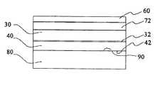
- FIG. 1is a cross section view of the first substrate with epitaxially grown graded Si 1 ⁇ x Ge x and relaxed Si 1 ⁇ y Ge y layers.
- FIG. 2is a cross section view of the first semiconductor substrate shown in FIG. 1 bonded to a second substrate with or without an insulator layer.
- FIG. 3is a cross section view of the first substrate shown in FIG. 2 thinned by grinding and polishing from its back side.
- FIG. 4is a cross section view of the remainder of the first substrate shown in FIG. 3 after the step of etching and stopping at the graded Si 1 ⁇ x Ge x layer by a highly selective wet etching process.
- FIG. 5is a cross section view of the remaining Si 1 ⁇ x Ge x layer from FIG. 4 polished away and the Si 1 ⁇ y Ge y layer smoothed with a chemical-mechanical planarization (CMP) process.
- CMPchemical-mechanical planarization
- FIG. 6is a cross section view of an epitaxially grown strained Si/SiGe layer or a p-i-n photodetector epitaxially grown over the smoothed Si 1 ⁇ y Ge y layer from FIG. 5 .
- FIG. 1a cross section view of a partial embodiment of the invention is shown comprising a substrate 10 and a plurality of layers 20 , 30 and 40 .
- Substrate 10may be a single crystal material such as Si, SiGe, SiGeC, SiC etc. suitable for forming epitaxial layers thereon.
- An epitaxial graded layer 20 of Si 1 ⁇ x Ge xis formed on the upper surface 12 of substrate 10 .
- the upper surface 22 of graded layer 20is substantially relaxed or completely relaxed. The relaxation may be due to a modified Frank-Read mechanism described by LeGoues et al. in U.S. Pat. No. 5,659,187 which issued on Aug. 19, 1997 and is incorporated herein by reference .
- a method for forming a graded SiGe layer 20is described in U.S. Pat. No. 5,659,187 by LeGoues et al.
- Layer 20 as well as layer 30may be formed in a UHV CVD process as described in U.S. Pat. No. 5,298,452 by B. S. Meyerson which issued Mar. 29, 1994 and is incorporated herein by reference.
- the concentration x of Gemay range from zero to a value in the range from 0.2 to 0.5.
- Layer 20may have a thickness in the range from about 3,000 angstroms to 1000 nm.
- Epitaxial layer 30is comprised substantially or completely of relaxed Si 1 ⁇ y Ge y and is formed on upper surface 22 of layer 20 .
- Layer 30may have a thickness in the range from 200 nm to 1000 nm.
- the Ge content y in layer 30is chosen to match the crystal lattice constant of upper surface 22 of layer 20 such that layer 30 is relaxed or essentially strain free.
- the Ge content y in layer 30may be equal to or about the value of x at upper surface 22 .
- the value ymay be in the range from about 0.2 to about 0.5.
- An encapsulation layer 40may be formed over relaxed layer 30 .
- Encapsulation layer 40may be formed on upper surface 32 of layer 30 via PECVD, LPCVD, UHV CVD or spin-on techniques.
- Encapsulation layer 40may have an upper surface 42 .
- the encapsulation materialmay be, for example, Si, SiO 2 , Poly Si, Si 3 N 4 , low-k dielectric materials, for example, Diamond Like Carbon (DLC), Fluorinated Diamond Like Carbon (FDLC), a polymer of Si, C, O, and H or a combination of any two or more of the foregoing materials.
- DLCDiamond Like Carbon
- FDLCFluorinated Diamond Like Carbon
- SiCOHOne example of a polymer of Si, C, O, and H is SiCOH which is described in Ser. No. 09/107567 filed Jun. 29, 1998 by Grill et al. entitled “Hydrogenated Oxidized Silicon Carbon Material” (Docket YOR919980245US1) which is incorporated herein by reference.
- the deposition temperature for forming layer 40may be below 900° C.
- the thickness of the encapsulation layeris in the range from about 5 nm to about 500 nm. Encapsulation layer 40 functions to protect upper surface 32 of layer 30 or to provide an isolation layer.
- a second substrate 80is bonded to upper surface 32 of layer 30 or to upper surface 42 of layer 40 .
- surface 32 of layer 30 or surface 42 of layer 40is polished by a Chemo-Mechanical Planarization or Polishing (CMP) process to smooth surface 42 to a planar surface having a surface roughness in root mean square (RMS) in the range from about 0.3 nm to about 1 nm.
- CMPChemo-Mechanical Planarization or Polishing
- Substrate 80which may be a semiconductor such as Si, SiGe, SiGeC, SiC, sapphire, glass, ceramic, or metal and has an upper surface 90 which may be polished as above to provide a smooth upper surface 90 having a RMS in the range from about 0.3 nm to about 1 nm.
- the top surface 42 of layer 40 shown in FIG. 1is turned upside down and brought into contact with surface 90 of substrate 80 .
- the two surfaces 42 and 90are brought together by the wafer bonding approach.
- the bonded surfaces or 42 and 90are annealed at a temperature in the range from about 20° C. to about 500° C. for a time period in the range from about 2 hours to about 50 hours.
- Another embodimentuses intermediate layers such as Ge, or metal materials which either have a low-melting point or react with silicon to form a silicide such materials may be tungsten (W), cobalt (Co), titanium (Ti) etc. to achieve high bonding strength at anneal temperatures in the range from 100° to 800° C.
- the annealcan be either a furnace anneal or a rapid thermal anneal (RTA).
- FIG. 3shows the removal of the majority of the first substrate 10 which is in the range from about 600 um to about 750 um in thickness with a grinding or a combination of grinding and polishing process.
- the remaining layer 70 of the first substrate 10has a thickness in the range from about 50 um to about 100 um.
- FIG. 4shows the removal of layer 70 such as with a wet etching process in a solution of ethylenediamine, pyrocatechol, pyrazine, water (EPPW or EDP) at a temperature in the range from about 90° C. to about 120° C. or in a solution of 20% KOH at a temperature in the range from about 70 to about 85° C. or in another organic Si etch solution of TMAH (tetramethyl ammoniumhydroxide, (CH 3 ) 4 NOH).
- TMAHtetramethyl ammoniumhydroxide, (CH 3 ) 4 NOH.
- EPPW, KOH or TMAHhas a much higher etching rate of Si compared to Si 1 ⁇ y Ge y (y>0.1), as a result, the etching process stops nicely at the relaxed Si 1 ⁇ y Ge y without any additional etch-stop layer such as the p ++ SiGe etch-stop as described in U.S. Pat. No. 5,906,951 which issued May 25, 1999 to J. O. Chu et al.
- FIG. 5shows the cross-section view of a SiGe layer on insulator or a SiGe/Si heterostructure after applying a CMP process step to remove the step-graded Si 1 ⁇ x Ge x layer 20 .
- the structurehas relaxed Si 1 ⁇ y Ge y layer 30 on top.
- the chemical-mechanical planarization (CMP) processis used to remove the graded Si 1 ⁇ x Ge x layer 20 and to adjust the thickness of the transferred relaxed Si 1 ⁇ y Ge y layer 30 .
- a final touch polishing and cleaningis used to smooth and clean the surface for epitaxial growth of strained Si/SiGe or for the deposition of a layer of n + Si as needed for form a p-i-n photodetector.
- a layer 60 of strained Si/SiGe or of n + Siis epitaxially grown or formed over SiGe layer 30 .
- an optional epitaxial SiGe buffer layer 72 over layer 30may be needed before the growth of the strained Si/SiGe layer 60 .
Landscapes
- Engineering & Computer Science (AREA)
- Microelectronics & Electronic Packaging (AREA)
- Condensed Matter Physics & Semiconductors (AREA)
- General Physics & Mathematics (AREA)
- Manufacturing & Machinery (AREA)
- Computer Hardware Design (AREA)
- Physics & Mathematics (AREA)
- Power Engineering (AREA)
- Recrystallisation Techniques (AREA)
- Element Separation (AREA)
- Bipolar Transistors (AREA)
- Junction Field-Effect Transistors (AREA)
- Thin Film Transistor (AREA)
Abstract
Description
- This invention relates to transferring a SiGe layer onto a second substrate and forming a new material structure that has emerging applications in microelectronics and optoelectronics. In particular, a strained Si/SiGe layer on an insulator structure is useful for fabricating high speed devices such as complementary metal oxide semiconductor (CMOS) transistors, modulation doped field effect transistors (MODFETs), high electron mobility transistors (HEMTs), and bipolar transistors (BTs); SiGe layer on Si heterostructures can be used to produce photodetectors to provide Si-based far infrared detection for communication, surveillance and medical applications.
- For applications in microelectronics, high carrier mobilities are desirable. It has been found that electron mobility in strained Si/SiGe channels is significantly higher than that in bulk Si. For example, measured values of electron mobility in strained Si at room temperature are about 3000 cm2/Vs as opposed to 400 cm2/Vs in bulk Si. Similarly, hole mobility in strained SiGe with high Ge concentration (60%˜80%) reaches up to 800 cm2/Vs the value of which is about 5 times the hole mobility of 150 cm2Vs in bulk Si. The use of these materials in state-of-the-art Si devices is expected to result in much higher performances, higher operating speeds in particular. However, the underlying conducting substrate for MODFETs and HBTs or the interaction of the underlying substrate with active device region in CMOS are undesirable features which limit the full implementation of high speed devices. To resolve the problem, an insulating layer is proposed to isolate the SiGe device layer from the substrate. Therefore, there is a need for techniques capable of fabricating strained Si/SiGe on insulator materials.
- There are two available techniques for making SiGe-On-Insulator (SGOI). One is via SIMOX as reported in a publication by T. Mizuno et al. entitled “High Performance Strained-Si p-MOSFETs on SiGe-on-Insulator Substrates Fabricated by SIMOX Technology,” IEDM, 99-934. However, this method has several limits because the oxygen implantation induces further damages in the relaxed SiGe layer in addition to the existing defects caused by lattice mismatch. And, the high temperature anneal (>1100° C.) needed to form oxide after the oxygen implantation is detrimental to the strained Si/SiGe layers since Ge tends to diffuse and agglomerate at temperatures above 600° C., this effect becomes more significant when Ge content is higher than 10%.
- The second technique of making SiGe on insulator is via selective etching with the aid of an etch stop. In U.S. Pat. No. 5,906,951 by J. O. Chu and K. E. Ismail which issued in May 1999, a method of utilizing wafer bonding and backside wafer etching in KOH with a p++-doped SiGe etch-stop to transfer a layer of strained Si/SiGe on a SOI substrate was described. However, the etching selectivity of SiGe to p++-doped SiGe etch-stop in KOH decreases sharply as the doping level in the etch stop layer is below 1019/cm3, therefore, the strained Si/SiGe layer may also be subjected to KOH etching if etching could not stop uniformly at the p++ SiGe etch-stop layer due to variation of dopants in the p++ etch-stop layer. Furthermore, since the SiGe etch-stop layer is heavily doped with boron in the range from about 5×10¹⁹to about 5×10²⁰/cm3, there are chances of auto-doping of the strained Si/SiGe during thermal treatment.
- For fiberoptic applications, SiGe/Si heterojunction diodes are a good choice for demodulating 1.3-1.6 um light at 300K. The use of 30% to 50% Ge is suggested to achieve absorption at the desired 1.3-1.6 um wavelength and low defects such as dislocations in the SiGe layer is needed to enhance the photodetector sensitivity. The state-of-the-art technology to achieve SiGe/Si heterojunction diodes with high responsivity, low noise, and fast response is to form a 100-period SiGe/Si strained layer superlattice. However, the alloy then no longer behaves like the bulk material due to the quantum size effect. The net result of the quantum size effect is that the absorption occurs at wavelengths (1.1-1.3 um) shorter than expected. Therefore, a bulk SiGe alloy with desirable Ge content and low defects is needed to fabricate photodetectors that would absorb lights in the range of 1.3-1.6 um.
- The invention provides a method capable of transferring a low defect SiGe layer onto a desirable substrate using the etch-back method but without any additional heavily doped etch-stop layer. The key feature of this invention is that a SiGe layer serves both as the layer over which the epitaxial strained Si/SiGe is grown but also as an etch-stop layer itself in some specific etching solutions. In other words, the SiGe layer is a self-etch-stop in this case. As a result, the process of fabricating strained Si/SiGe on insulator or a SiGe/Si heterostucture is greatly simplified and the quality of the strained Si/SiGe or SiGe/Si heterostucture is significantly improved.
- In accordance with the present invention, a method for transferring low defect SiGe bulk layer onto a second substrate and forming strained Si/SiGe on an insulator (SGOI) or SiGe/Si heterostructure is described. This approach comprises the steps of selecting a semiconductor substrate, forming a first expitaxial graded layer of Si1−xGexover the semiconductor substrate, forming a second relaxed Si1−yGeyover the first graded Si1−xGexlayer, selecting a second substrate, bonding the first substrate to said second substrate to form a joined substrate, grinding and polishing the first substrate from its backside to remove the majority of said first substrate, etching the remaining material of the first substrate and stopping at the Si1−xGexutilizing a SiGe highly selective wet etch process, applying chemical-mechanical planarization (CMP) to remove the defective portion of the graded Si1−xGexlayer, smoothing the surface of the Si1−xGxlayer by a CMP process step, growing strained Si/SiGe layers over the smoothed surface of the Si1−xGexlayer for MOSFET, MODFET, HEMT or BT for microelectronic applications, or growing SiGe photodectors for applications in optoelectronics.
- The invention provides a method capable of transferring a low defect SiGe layer onto a desirable substrate using the etch-back method but without any additional heavily doped etch-stop layer. The key feature of this invention is that a SiGe layer serves both as the layer over which the epitaxial strained Si/SiGe is grown but also as an etch-stop layer itself in some specific etching solutions. In other words, the SiGe layer is a self-etch-stop in this case. As a result, the process of fabricating strained Si/SiGe on insulator or a SiGe/Si heterostucture is greatly simplified and the quality of the strained Si/SiGe or SiGe/Si heterostucture is significantly improved.
- The invention is described in more details thereinafter relative to non-limitative embodiments and with reference to the attached drawings, wherein show:
FIG. 1 is a cross section view of the first substrate with epitaxially grown graded Si1−xGexand relaxed Si1−yGeylayers.FIG. 2 is a cross section view of the first semiconductor substrate shown inFIG. 1 bonded to a second substrate with or without an insulator layer.FIG. 3 is a cross section view of the first substrate shown inFIG. 2 thinned by grinding and polishing from its back side.FIG. 4 is a cross section view of the remainder of the first substrate shown inFIG. 3 after the step of etching and stopping at the graded Si1−xGexlayer by a highly selective wet etching process.FIG. 5 is a cross section view of the remaining Si1−xGexlayer fromFIG. 4 polished away and the Si1−yGeylayer smoothed with a chemical-mechanical planarization (CMP) process.FIG. 6 is a cross section view of an epitaxially grown strained Si/SiGe layer or a p-i-n photodetector epitaxially grown over the smoothed Si1−yGeylayer fromFIG. 5 .- The embodiment which will now be described in conjunction with the above drawings relates to the formation of a layer of monocrystalline strained Si/SiGe on an insulator material (SGOI) or a SiGe layer on Si with the aid of planarization of surfaces, wafer bonding and a selective wet etching process using SiGe as the etch-stop layer.
- Referring now to
FIG. 1 , a cross section view of a partial embodiment of the invention is shown comprising asubstrate 10 and a plurality oflayers Substrate 10 may be a single crystal material such as Si, SiGe, SiGeC, SiC etc. suitable for forming epitaxial layers thereon. An epitaxial gradedlayer 20 of Si1−xGexis formed on theupper surface 12 ofsubstrate 10. Theupper surface 22 of gradedlayer 20 is substantially relaxed or completely relaxed. The relaxation may be due to a modified Frank-Read mechanism described by LeGoues et al. in U.S. Pat. No. 5,659,187 which issued on Aug. 19, 1997 and is incorporated herein by reference . A method for forming a gradedSiGe layer 20 is described in U.S. Pat. No. 5,659,187 by LeGoues et al.Layer 20 as well as layer30 (to be described below) may be formed in a UHV CVD process as described in U.S. Pat. No. 5,298,452 by B. S. Meyerson which issued Mar. 29, 1994 and is incorporated herein by reference. Inlayer 20, the concentration x of Ge may range from zero to a value in the range from 0.2 to 0.5.Layer 20 may have a thickness in the range from about 3,000 angstroms to 1000 nm. Epitaxial layer 30 is comprised substantially or completely of relaxed Si1−yGeyand is formed onupper surface 22 oflayer 20.Layer 30 may have a thickness in the range from 200 nm to 1000 nm. The Ge content y inlayer 30 is chosen to match the crystal lattice constant ofupper surface 22 oflayer 20 such thatlayer 30 is relaxed or essentially strain free. The Ge content y inlayer 30 may be equal to or about the value of x atupper surface 22. The value y may be in the range from about 0.2 to about 0.5. Anencapsulation layer 40 may be formed overrelaxed layer 30.Encapsulation layer 40 may be formed onupper surface 32 oflayer 30 via PECVD, LPCVD, UHV CVD or spin-on techniques.Encapsulation layer 40 may have anupper surface 42. The encapsulation material may be, for example, Si, SiO2, Poly Si, Si3N4, low-k dielectric materials, for example, Diamond Like Carbon (DLC), Fluorinated Diamond Like Carbon (FDLC), a polymer of Si, C, O, and H or a combination of any two or more of the foregoing materials. One example of a polymer of Si, C, O, and H is SiCOH which is described in Ser. No. 09/107567 filed Jun. 29, 1998 by Grill et al. entitled “Hydrogenated Oxidized Silicon Carbon Material” (Docket YOR919980245US1) which is incorporated herein by reference. The deposition temperature for forminglayer 40 may be below 900° C. The thickness of the encapsulation layer is in the range from about 5 nm to about 500 nm.Encapsulation layer 40 functions to protectupper surface 32 oflayer 30 or to provide an isolation layer.- In
FIG. 2 , asecond substrate 80 is bonded toupper surface 32 oflayer 30 or toupper surface 42 oflayer 40. Prior to wafer bonding,surface 32 oflayer 30 orsurface 42 oflayer 40 is polished by a Chemo-Mechanical Planarization or Polishing (CMP) process to smoothsurface 42 to a planar surface having a surface roughness in root mean square (RMS) in the range from about 0.3 nm to about 1 nm.Substrate 80 which may be a semiconductor such as Si, SiGe, SiGeC, SiC, sapphire, glass, ceramic, or metal and has anupper surface 90 which may be polished as above to provide a smoothupper surface 90 having a RMS in the range from about 0.3 nm to about 1 nm. - For a further description on polishing to reduce surface roughness, reference is made to Ser. No. 09/675841 filed Sep. 29, 2000 by D. F. Canaperi et al. entitled “A Method of Wafer Smoothing for Bonding Using Chemo-Mechanical Polishing (CMP)” (Docket No. YOR920000683US1) which is incorporated herein by reference.
- For a further description on bonding wafers to provide a bonded structure, reference is made to Ser. No. 09/675840 filed Sep. 29, 2000 by D. F. Canaperi et al. entitled “Preparation of Strained Si/SiGe on Insulator by Hydrogen Induced Layer Transfer Technique” (Docket No. YOR920000345US1) which is incorporated herein by reference. The method of making SGOI by wafer bonding and H-implantation induced layer transfer is described in Ser. No. 09/675840. This method can produce SiGe with higher Ge content onto an insulator compared to the prior art. Further, this method can reduce the amount of defects in the SiGe layer due to the elimination of the misfit dislocations compared to the prior art. However, with this method, the transferred SiGe layer is relatively thin (<1 um) and transferring a high Ge content layer is still difficult to achieve due to implantation of H and annealing at 500 to 600° C. to induce layer transfer.
- The
top surface 42 oflayer 40 shown inFIG. 1 is turned upside down and brought into contact withsurface 90 ofsubstrate 80. The twosurfaces FIG. 3 shows the removal of the majority of thefirst substrate 10 which is in the range from about 600 um to about 750 um in thickness with a grinding or a combination of grinding and polishing process. The remaininglayer 70 of thefirst substrate 10 has a thickness in the range from about 50 um to about 100 um.FIG. 4 shows the removal oflayer 70 such as with a wet etching process in a solution of ethylenediamine, pyrocatechol, pyrazine, water (EPPW or EDP) at a temperature in the range from about 90° C. to about 120° C. or in a solution of 20% KOH at a temperature in the range from about 70 to about 85° C. or in another organic Si etch solution of TMAH (tetramethyl ammoniumhydroxide, (CH3)4NOH). The etching selectivity of Si (100) to Si1−xGex(y=0.15˜0.3) in EPPW is experimentally determined to be in the range of 50-1800. The etching selectivity of Si (100) to Si1−xGex(y=0.2˜0.3) in KOH is experimentally determined to be in the range of 350-1280, and the etching selectivity of Si (100) to Si1−xGex(y=0.2˜0.3) in TMAH is experimentally determined to be in the range of 50-115. In a prior art of U.S. Pat. No. 5,476,813 which issued Dec. 19, 1995 to H. Naruse by a mixed solution of KOH, K2Cr2O7, and propanol is used for selective etching of silicon while stopping at SiGe layer. However, a much lower selectivity of about 17 to 20 is achieved. In our invention, EPPW, KOH or TMAH has a much higher etching rate of Si compared to Si1−yGey(y>0.1), as a result, the etching process stops nicely at the relaxed Si1−yGeywithout any additional etch-stop layer such as the p++ SiGe etch-stop as described in U.S. Pat. No. 5,906,951 which issued May 25, 1999 to J. O. Chu et al.FIG. 5 shows the cross-section view of a SiGe layer on insulator or a SiGe/Si heterostructure after applying a CMP process step to remove the step-graded Si1−xGexlayer20. The structure has relaxed Si1−yGeylayer30 on top. The chemical-mechanical planarization (CMP) process is used to remove the graded Si1−xGexlayer20 and to adjust the thickness of the transferred relaxed Si1−yGeylayer30. A final touch polishing and cleaning is used to smooth and clean the surface for epitaxial growth of strained Si/SiGe or for the deposition of a layer of n+ Si as needed for form a p-i-n photodetector.- In
FIG. 6 , alayer 60 of strained Si/SiGe or of n+ Si is epitaxially grown or formed overSiGe layer 30. For the epitaxial growth of strained Si/SiGe layer, an optional epitaxialSiGe buffer layer 72 overlayer 30 may be needed before the growth of the strained Si/SiGe layer 60. - It should be noted in the drawing that like elements or components are referred to by like and corresponding reference numerals.
- While there has been described and illustrated a method for forming strained Si or SiGe on SiGe on insulator (SGOI) or strained SiGe/Si heterostructure using wafer bonding and wet etching, it will be apparent to those skilled in the art that modifications and variations are possible without deviating from the broad scope of the invention which shall be limited solely by the scope of the claims appended hereto.
Claims (42)
Priority Applications (3)
| Application Number | Priority Date | Filing Date | Title |
|---|---|---|---|
| US10/948,421US7427773B2 (en) | 2000-10-19 | 2004-09-23 | Layer transfer of low defect SiGe using an etch-back process |
| US12/181,489US20090026495A1 (en) | 2000-10-19 | 2008-07-29 | LAYER TRANSFER OF LOW DEFECT SiGe USING AN ETCH-BACK PROCESS |
| US12/181,613US7786468B2 (en) | 2000-10-19 | 2008-07-29 | Layer transfer of low defect SiGe using an etch-back process |
Applications Claiming Priority (2)
| Application Number | Priority Date | Filing Date | Title |
|---|---|---|---|
| US09/692,606US6890835B1 (en) | 2000-10-19 | 2000-10-19 | Layer transfer of low defect SiGe using an etch-back process |
| US10/948,421US7427773B2 (en) | 2000-10-19 | 2004-09-23 | Layer transfer of low defect SiGe using an etch-back process |
Related Parent Applications (1)
| Application Number | Title | Priority Date | Filing Date |
|---|---|---|---|
| US09/692,606DivisionUS6890835B1 (en) | 2000-10-19 | 2000-10-19 | Layer transfer of low defect SiGe using an etch-back process |
Related Child Applications (2)
| Application Number | Title | Priority Date | Filing Date |
|---|---|---|---|
| US12/181,489DivisionUS20090026495A1 (en) | 2000-10-19 | 2008-07-29 | LAYER TRANSFER OF LOW DEFECT SiGe USING AN ETCH-BACK PROCESS |
| US12/181,613DivisionUS7786468B2 (en) | 2000-10-19 | 2008-07-29 | Layer transfer of low defect SiGe using an etch-back process |
Publications (2)
| Publication Number | Publication Date |
|---|---|
| US20050104067A1true US20050104067A1 (en) | 2005-05-19 |
| US7427773B2 US7427773B2 (en) | 2008-09-23 |
Family
ID=24781275
Family Applications (4)
| Application Number | Title | Priority Date | Filing Date |
|---|---|---|---|
| US09/692,606Expired - Fee RelatedUS6890835B1 (en) | 2000-10-19 | 2000-10-19 | Layer transfer of low defect SiGe using an etch-back process |
| US10/948,421Expired - Fee RelatedUS7427773B2 (en) | 2000-10-19 | 2004-09-23 | Layer transfer of low defect SiGe using an etch-back process |
| US12/181,489AbandonedUS20090026495A1 (en) | 2000-10-19 | 2008-07-29 | LAYER TRANSFER OF LOW DEFECT SiGe USING AN ETCH-BACK PROCESS |
| US12/181,613Expired - Fee RelatedUS7786468B2 (en) | 2000-10-19 | 2008-07-29 | Layer transfer of low defect SiGe using an etch-back process |
Family Applications Before (1)
| Application Number | Title | Priority Date | Filing Date |
|---|---|---|---|
| US09/692,606Expired - Fee RelatedUS6890835B1 (en) | 2000-10-19 | 2000-10-19 | Layer transfer of low defect SiGe using an etch-back process |
Family Applications After (2)
| Application Number | Title | Priority Date | Filing Date |
|---|---|---|---|
| US12/181,489AbandonedUS20090026495A1 (en) | 2000-10-19 | 2008-07-29 | LAYER TRANSFER OF LOW DEFECT SiGe USING AN ETCH-BACK PROCESS |
| US12/181,613Expired - Fee RelatedUS7786468B2 (en) | 2000-10-19 | 2008-07-29 | Layer transfer of low defect SiGe using an etch-back process |
Country Status (9)
| Country | Link |
|---|---|
| US (4) | US6890835B1 (en) |
| EP (1) | EP1327263A1 (en) |
| JP (1) | JP2004512683A (en) |
| KR (1) | KR100613182B1 (en) |
| CN (1) | CN100472748C (en) |
| AU (1) | AU2001287881A1 (en) |
| IL (2) | IL155395A0 (en) |
| TW (1) | TW521395B (en) |
| WO (1) | WO2002033746A1 (en) |
Cited By (10)
| Publication number | Priority date | Publication date | Assignee | Title |
|---|---|---|---|---|
| US20050280026A1 (en)* | 2004-06-16 | 2005-12-22 | Isaacson David M | Strained silicon-on-silicon by wafer bonding and layer transfer |
| US20070218647A1 (en)* | 2004-09-13 | 2007-09-20 | International Business Machines Corporation | METHOD OF CREATING DEFECT FREE HIGH Ge CONTENT (> 25%) SiGe-ON-INSULATOR (SGOI) SUBSTRATES USING WAFER BONDING TECHNIQUES |
| US20080128868A1 (en)* | 2004-12-24 | 2008-06-05 | Tracit Technologies | Method of Transferring a Circuit Onto a Ground Plane |
| US7538008B2 (en) | 2006-05-04 | 2009-05-26 | Siltronic Ag | Method for producing a layer structure |
| US20090206348A1 (en)* | 2006-04-25 | 2009-08-20 | Osram Opto Semiconductors Gmbh | Composite Substrate, and Method for the Production of a Composite Substrate |
| US20110272694A1 (en)* | 2007-12-27 | 2011-11-10 | Michiko Takei | Insulating substrate for semiconductor apparatus, semiconductor apparatus, and method for manufacturing semiconductor apparatus |
| US20140183601A1 (en)* | 2011-06-23 | 2014-07-03 | Soitec | Method for transferring a layer of a semiconductor and substrate comprising a confinement structure |
| US11056382B2 (en) | 2018-03-19 | 2021-07-06 | Globalfoundries U.S. Inc. | Cavity formation within and under semiconductor devices |
| US20220130866A1 (en)* | 2019-03-04 | 2022-04-28 | Board Of Regents, The University Of Texas System | Silicon-On-Oxide-On-Silicon |
| US20230025306A1 (en)* | 2021-07-23 | 2023-01-26 | Commissariat à l'énergie atomique et aux énergies alternatives | Method for manufacturing a soi or sigeoi type semiconductor-on-insulator substrate by besoi and structure for manufacturing such a substrate |
Families Citing this family (72)
| Publication number | Priority date | Publication date | Assignee | Title |
|---|---|---|---|---|
| US7227176B2 (en)* | 1998-04-10 | 2007-06-05 | Massachusetts Institute Of Technology | Etch stop layer system |
| JP3883784B2 (en)* | 2000-05-24 | 2007-02-21 | 三洋電機株式会社 | Plate-shaped body and method for manufacturing semiconductor device |
| US6830976B2 (en) | 2001-03-02 | 2004-12-14 | Amberwave Systems Corproation | Relaxed silicon germanium platform for high speed CMOS electronics and high speed analog circuits |
| US6703688B1 (en) | 2001-03-02 | 2004-03-09 | Amberwave Systems Corporation | Relaxed silicon germanium platform for high speed CMOS electronics and high speed analog circuits |
| WO2002082514A1 (en) | 2001-04-04 | 2002-10-17 | Massachusetts Institute Of Technology | A method for semiconductor device fabrication |
| US6717213B2 (en)* | 2001-06-29 | 2004-04-06 | Intel Corporation | Creation of high mobility channels in thin-body SOI devices |
| JP2003249641A (en)* | 2002-02-22 | 2003-09-05 | Sharp Corp | Semiconductor substrate, method of manufacturing the same, and semiconductor device |
| US20030227057A1 (en) | 2002-06-07 | 2003-12-11 | Lochtefeld Anthony J. | Strained-semiconductor-on-insulator device structures |
| US6995430B2 (en) | 2002-06-07 | 2006-02-07 | Amberwave Systems Corporation | Strained-semiconductor-on-insulator device structures |
| US7074623B2 (en)* | 2002-06-07 | 2006-07-11 | Amberwave Systems Corporation | Methods of forming strained-semiconductor-on-insulator finFET device structures |
| JP2004014856A (en)* | 2002-06-07 | 2004-01-15 | Sharp Corp | Method for manufacturing semiconductor substrate and method for manufacturing semiconductor device |
| US7157119B2 (en) | 2002-06-25 | 2007-01-02 | Ppg Industries Ohio, Inc. | Method and compositions for applying multiple overlying organic pigmented decorations on ceramic substrates |
| US6936869B2 (en)* | 2002-07-09 | 2005-08-30 | International Rectifier Corporation | Heterojunction field effect transistors using silicon-germanium and silicon-carbon alloys |
| US7018910B2 (en) | 2002-07-09 | 2006-03-28 | S.O.I.Tec Silicon On Insulator Technologies S.A. | Transfer of a thin layer from a wafer comprising a buffer layer |
| US6841457B2 (en)* | 2002-07-16 | 2005-01-11 | International Business Machines Corporation | Use of hydrogen implantation to improve material properties of silicon-germanium-on-insulator material made by thermal diffusion |
| US6707106B1 (en)* | 2002-10-18 | 2004-03-16 | Advanced Micro Devices, Inc. | Semiconductor device with tensile strain silicon introduced by compressive material in a buried oxide layer |
| KR100874788B1 (en)* | 2003-01-07 | 2008-12-18 | 에스. 오. 이. 떼끄 씰리꽁 오 냉쉴라또흐 떼끄놀로지 | Recycling method by mechanical means of a wafer including a peeling structure after thin layer peeling |
| US20090325362A1 (en)* | 2003-01-07 | 2009-12-31 | Nabil Chhaimi | Method of recycling an epitaxied donor wafer |
| JP4659732B2 (en)* | 2003-01-27 | 2011-03-30 | 台湾積體電路製造股▲ふん▼有限公司 | Method for forming a semiconductor layer |
| US7049660B2 (en)* | 2003-05-30 | 2006-05-23 | International Business Machines Corporation | High-quality SGOI by oxidation near the alloy melting temperature |
| US6855963B1 (en)* | 2003-08-29 | 2005-02-15 | International Business Machines Corporation | Ultra high-speed Si/SiGe modulation-doped field effect transistors on ultra thin SOI/SGOI substrate |
| US7029980B2 (en) | 2003-09-25 | 2006-04-18 | Freescale Semiconductor Inc. | Method of manufacturing SOI template layer |
| FR2860340B1 (en) | 2003-09-30 | 2006-01-27 | Soitec Silicon On Insulator | INDIRECT BONDING WITH DISAPPEARANCE OF THE BONDING LAYER |
| JP2005109346A (en) | 2003-10-01 | 2005-04-21 | Seiko Epson Corp | Semiconductor device and manufacturing method of semiconductor device |
| FR2863771B1 (en)* | 2003-12-10 | 2007-03-02 | Soitec Silicon On Insulator | PROCESS FOR PROCESSING A MULTILAYER WAFER HAVING A DIFFERENTIAL OF THERMAL CHARACTERISTICS |
| JP4700324B2 (en)* | 2003-12-25 | 2011-06-15 | シルトロニック・ジャパン株式会社 | Manufacturing method of semiconductor substrate |
| US20060124961A1 (en)* | 2003-12-26 | 2006-06-15 | Canon Kabushiki Kaisha | Semiconductor substrate, manufacturing method thereof, and semiconductor device |
| JP2005210062A (en)* | 2003-12-26 | 2005-08-04 | Canon Inc | Semiconductor member, manufacturing method thereof, and semiconductor device |
| US7550370B2 (en)* | 2004-01-16 | 2009-06-23 | International Business Machines Corporation | Method of forming thin SGOI wafers with high relaxation and low stacking fault defect density |
| US7064396B2 (en) | 2004-03-01 | 2006-06-20 | Freescale Semiconductor, Inc. | Integrated circuit with multiple spacer insulating region widths |
| US7241647B2 (en) | 2004-08-17 | 2007-07-10 | Freescale Semiconductor, Inc. | Graded semiconductor layer |
| KR100612892B1 (en)* | 2004-11-12 | 2006-08-14 | 삼성전자주식회사 | Semiconductor device and fabricating method of the same |
| US7393733B2 (en) | 2004-12-01 | 2008-07-01 | Amberwave Systems Corporation | Methods of forming hybrid fin field-effect transistor structures |
| US7282402B2 (en) | 2005-03-30 | 2007-10-16 | Freescale Semiconductor, Inc. | Method of making a dual strained channel semiconductor device |
| US8007675B1 (en)* | 2005-07-11 | 2011-08-30 | National Semiconductor Corporation | System and method for controlling an etch process for a single crystal having a buried layer |
| US20070117350A1 (en)* | 2005-08-03 | 2007-05-24 | Memc Electronic Materials, Inc. | Strained silicon on insulator (ssoi) with layer transfer from oxidized donor |
| DE102006007293B4 (en)* | 2006-01-31 | 2023-04-06 | OSRAM Opto Semiconductors Gesellschaft mit beschränkter Haftung | Method for producing a quasi-substrate wafer and a semiconductor body produced using such a quasi-substrate wafer |
| US7923353B2 (en)* | 2006-03-27 | 2011-04-12 | Okmetic Oyj | Gettering method and a wafer using the same |
| EP2016618A1 (en)* | 2006-04-24 | 2009-01-21 | Sören Berg | Hybrid wafers |
| KR100765024B1 (en)* | 2006-06-21 | 2007-10-09 | 닛산 지도우샤 가부시키가이샤 | Manufacturing Method of Semiconductor Device |
| EP1928020B1 (en)* | 2006-11-30 | 2020-04-22 | Soitec | Method of manufacturing a semiconductor heterostructure |
| US7893475B2 (en)* | 2007-01-24 | 2011-02-22 | Macronix International Co., Ltd. | Dynamic random access memory cell and manufacturing method thereof |
| JP5465830B2 (en)* | 2007-11-27 | 2014-04-09 | 信越化学工業株式会社 | Manufacturing method of bonded substrate |
| FR2929758B1 (en)* | 2008-04-07 | 2011-02-11 | Commissariat Energie Atomique | TRANSFER METHOD USING A FERROELECTRIC SUBSTRATE |
| US8058143B2 (en)* | 2009-01-21 | 2011-11-15 | Freescale Semiconductor, Inc. | Substrate bonding with metal germanium silicon material |
| GB2501432B (en)* | 2009-02-19 | 2013-12-04 | Iqe Silicon Compounds Ltd | Photovoltaic cell |
| GB2467934B (en)* | 2009-02-19 | 2013-10-30 | Iqe Silicon Compounds Ltd | Photovoltaic cell |
| GB2467935B (en) | 2009-02-19 | 2013-10-30 | Iqe Silicon Compounds Ltd | Formation of thin layers of GaAs and germanium materials |
| JP5397079B2 (en)* | 2009-08-11 | 2014-01-22 | ソニー株式会社 | Video signal processing apparatus, enhancement gain generation method, and program |
| US20110086444A1 (en)* | 2009-10-14 | 2011-04-14 | Taiwan Semiconductor Manufacturing Company, Ltd. | Process for producing substrates free of patterns using an alpha stepper to ensure results |
| JP2011254051A (en)* | 2010-06-04 | 2011-12-15 | Sumitomo Electric Ind Ltd | Silicon carbide substrate manufacturing method, semiconductor device manufacturing method, silicon carbide substrate and semiconductor device |
| CN102376876B (en)* | 2010-08-05 | 2013-09-18 | 中芯国际集成电路制造(上海)有限公司 | Phase change nonvolatile memory and processing method thereof |
| US8486744B2 (en)* | 2010-09-28 | 2013-07-16 | Taiwan Semiconductor Manufacturing Company, Ltd. | Multiple bonding in wafer level packaging |
| CN102299093A (en)* | 2011-06-30 | 2011-12-28 | 上海新傲科技股份有限公司 | Method for preparing semiconductor substrate with insulation burying layer and semiconductor substrate |
| KR20140071353A (en)* | 2011-08-01 | 2014-06-11 | 바스프 에스이 | Method of manufacturing semiconductor devices comprising chemical mechanical polishing of elemental germanium and / or Si 1 x Gex material in the presence of a chemical mechanical polishing composition having a pH value of 3.0 to 5.5 |
| CN103165512A (en)* | 2011-12-14 | 2013-06-19 | 中国科学院上海微系统与信息技术研究所 | Extremely thin semiconductor-on-insulator material and preparation method thereof |
| CN103165511B (en)* | 2011-12-14 | 2015-07-22 | 中国科学院上海微系统与信息技术研究所 | Method for manufacturing germanium on insulator (GOI) |
| CN102637607B (en)* | 2011-12-29 | 2016-02-24 | 上海新傲科技股份有限公司 | Three-dimension packaging method |
| US10084063B2 (en)* | 2014-06-23 | 2018-09-25 | Taiwan Semiconductor Manufacturing Company Ltd. | Semiconductor device and manufacturing method thereof |
| WO2015198117A1 (en) | 2014-06-26 | 2015-12-30 | Soitec | Semiconductor structures including bonding layers, multijunction photovoltaic cells and related methods |
| CN105845546B (en) | 2015-01-15 | 2019-11-05 | 联华电子股份有限公司 | Epitaxial manufacturing process of illumination |
| CN105990472A (en)* | 2015-02-04 | 2016-10-05 | 深圳市立洋光电子有限公司 | Surface treatment method of silicon substrate LED luminous chip |
| CN107667416B (en)* | 2015-06-01 | 2021-08-31 | 环球晶圆股份有限公司 | Method of making semiconductor-on-insulator |
| SG11201802818VA (en)* | 2015-10-13 | 2018-05-30 | Univ Nanyang Tech | Method of manufacturing a germanium-on-insulator substrate |
| FR3049761B1 (en)* | 2016-03-31 | 2018-10-05 | Soitec | METHOD FOR MANUFACTURING A STRUCTURE FOR FORMING A THREE DIMENSIONAL MONOLITHIC INTEGRATED CIRCUIT |
| EP3252800A1 (en)* | 2016-05-31 | 2017-12-06 | Laser Systems & Solutions of Europe | Deep junction electronic device and process for manufacturing thereof |
| KR101889352B1 (en) | 2016-09-13 | 2018-08-20 | 한국과학기술연구원 | Semicondutor device including strained germanium and method for manufacturing the same |
| FR3064398B1 (en)* | 2017-03-21 | 2019-06-07 | Soitec | SEMICONDUCTOR TYPE STRUCTURE ON INSULATION, ESPECIALLY FOR A FRONT-SIDE TYPE IMAGE SENSOR, AND METHOD FOR MANUFACTURING SUCH STRUCTURE |
| CN107302037B (en)* | 2017-06-12 | 2019-05-17 | 北京工业大学 | The SiGe/Si Heterojunction phototransistor detector of base area Ge component segmentation distribution |
| CN108878263B (en)* | 2018-06-25 | 2022-03-18 | 中国科学院微电子研究所 | Semiconductor structure and manufacturing method thereof |
| TWI788869B (en)* | 2021-06-04 | 2023-01-01 | 合晶科技股份有限公司 | High electron mobility transistor and composite substrate thereof |
| US11923237B2 (en)* | 2021-08-30 | 2024-03-05 | Taiwan Semiconductor Manufacturing Company, Ltd. | Manufacturing method of semiconductor device |
Citations (20)
| Publication number | Priority date | Publication date | Assignee | Title |
|---|---|---|---|---|
| US4826787A (en)* | 1986-03-18 | 1989-05-02 | Fujitsu Limited | Method for adhesion of silicon or silicon dioxide plate |
| US5013681A (en)* | 1989-09-29 | 1991-05-07 | The United States Of America As Represented By The Secretary Of The Navy | Method of producing a thin silicon-on-insulator layer |
| US5240876A (en)* | 1991-02-22 | 1993-08-31 | Harris Corporation | Method of fabricating SOI wafer with SiGe as an etchback film in a BESOI process |
| US5298452A (en)* | 1986-09-12 | 1994-03-29 | International Business Machines Corporation | Method and apparatus for low temperature, low pressure chemical vapor deposition of epitaxial silicon layers |
| US5387555A (en)* | 1992-09-03 | 1995-02-07 | Harris Corporation | Bonded wafer processing with metal silicidation |
| US5462883A (en)* | 1991-06-28 | 1995-10-31 | International Business Machines Corporation | Method of fabricating defect-free silicon on an insulating substrate |
| US5476813A (en)* | 1993-11-15 | 1995-12-19 | Kabushiki Kaisha Toshiba | Method of manufacturing a bonded semiconductor substrate and a dielectric isolated bipolar transistor |
| US5650353A (en)* | 1992-09-29 | 1997-07-22 | Shin-Etsu Handotai Co., Ltd. | Method for production of SOI substrate |
| US5659187A (en)* | 1991-05-31 | 1997-08-19 | International Business Machines Corporation | Low defect density/arbitrary lattice constant heteroepitaxial layers |
| US5906951A (en)* | 1997-04-30 | 1999-05-25 | International Business Machines Corporation | Strained Si/SiGe layers on insulator |
| US6103597A (en)* | 1996-04-11 | 2000-08-15 | Commissariat A L'energie Atomique | Method of obtaining a thin film of semiconductor material |
| US6118181A (en)* | 1998-07-29 | 2000-09-12 | Agilent Technologies, Inc. | System and method for bonding wafers |
| US6153495A (en)* | 1998-03-09 | 2000-11-28 | Intersil Corporation | Advanced methods for making semiconductor devices by low temperature direct bonding |
| US6255731B1 (en)* | 1997-07-30 | 2001-07-03 | Canon Kabushiki Kaisha | SOI bonding structure |
| US6323108B1 (en)* | 1999-07-27 | 2001-11-27 | The United States Of America As Represented By The Secretary Of The Navy | Fabrication ultra-thin bonded semiconductor layers |
| US6328796B1 (en)* | 1999-02-01 | 2001-12-11 | The United States Of America As Represented By The Secretary Of The Navy | Single-crystal material on non-single-crystalline substrate |
| US20020072130A1 (en)* | 2000-08-16 | 2002-06-13 | Zhi-Yuan Cheng | Process for producing semiconductor article using graded expital growth |
| US6521041B2 (en)* | 1998-04-10 | 2003-02-18 | Massachusetts Institute Of Technology | Etch stop layer system |
| US6524935B1 (en)* | 2000-09-29 | 2003-02-25 | International Business Machines Corporation | Preparation of strained Si/SiGe on insulator by hydrogen induced layer transfer technique |
| US6689211B1 (en)* | 1999-04-09 | 2004-02-10 | Massachusetts Institute Of Technology | Etch stop layer system |
Family Cites Families (16)
| Publication number | Priority date | Publication date | Assignee | Title |
|---|---|---|---|---|
| US5230768A (en)* | 1990-03-26 | 1993-07-27 | Sharp Kabushiki Kaisha | Method for the production of SiC single crystals by using a specific substrate crystal orientation |
| JPH0515453A (en) | 1991-07-09 | 1993-01-26 | Matsushita Electric Ind Co Ltd | Water heater |
| JPH0515453U (en)* | 1991-08-05 | 1993-02-26 | 横河電機株式会社 | SOI substrate |
| JP2959352B2 (en)* | 1993-08-10 | 1999-10-06 | 信越半導体株式会社 | Method of manufacturing semiconductor wafer and analysis method by SIMS |
| JP3265493B2 (en)* | 1994-11-24 | 2002-03-11 | ソニー株式会社 | Method for manufacturing SOI substrate |
| JPH08148659A (en)* | 1994-11-24 | 1996-06-07 | Mitsubishi Materials Corp | Manufacture of soi substrate |
| JP3441277B2 (en)* | 1995-12-26 | 2003-08-25 | 株式会社東芝 | Semiconductor device and manufacturing method thereof |
| JP3443343B2 (en)* | 1997-12-03 | 2003-09-02 | 松下電器産業株式会社 | Semiconductor device |
| EP0991126B1 (en)* | 1997-12-09 | 2006-10-18 | Seiko Epson Corporation | Method of manufacturing an electrooptic device |
| JP2000031491A (en)* | 1998-07-14 | 2000-01-28 | Hitachi Ltd | Semiconductor device, method of manufacturing semiconductor device, semiconductor substrate, and method of manufacturing semiconductor substrate |
| AU1717600A (en)* | 1998-11-10 | 2000-05-29 | Biocrystal Limited | Methods for identification and verification |
| CN1168147C (en)* | 1999-01-14 | 2004-09-22 | 松下电器产业株式会社 | Manufacturing method of semiconductor crystal |
| JP3607194B2 (en)* | 1999-11-26 | 2005-01-05 | 株式会社東芝 | Semiconductor device, semiconductor device manufacturing method, and semiconductor substrate |
| US6550353B2 (en)* | 2000-06-07 | 2003-04-22 | The Gates Corporation | Geared drive ring coupler |
| US6656313B2 (en)* | 2001-06-11 | 2003-12-02 | International Business Machines Corporation | Structure and method for improved adhesion between two polymer films |
| WO2003017336A2 (en)* | 2001-08-13 | 2003-02-27 | Amberwave Systems Corporation | Dram trench capacitor and method of making the same |
- 2000
- 2000-10-19USUS09/692,606patent/US6890835B1/ennot_activeExpired - Fee Related
- 2001
- 2001-09-17CNCNB018176550Apatent/CN100472748C/ennot_activeExpired - Fee Related
- 2001-09-17KRKR1020037005157Apatent/KR100613182B1/ennot_activeExpired - Fee Related
- 2001-09-17AUAU2001287881Apatent/AU2001287881A1/ennot_activeAbandoned
- 2001-09-17ILIL15539501Apatent/IL155395A0/ennot_activeIP Right Cessation
- 2001-09-17JPJP2002537047Apatent/JP2004512683A/ennot_activeWithdrawn
- 2001-09-17EPEP01967506Apatent/EP1327263A1/ennot_activeWithdrawn
- 2001-09-17WOPCT/GB2001/004159patent/WO2002033746A1/enactiveApplication Filing
- 2001-10-16TWTW090125554Apatent/TW521395B/ennot_activeIP Right Cessation
- 2003
- 2003-04-11ILIL155395Apatent/IL155395A/ennot_activeIP Right Cessation
- 2004
- 2004-09-23USUS10/948,421patent/US7427773B2/ennot_activeExpired - Fee Related
- 2008
- 2008-07-29USUS12/181,489patent/US20090026495A1/ennot_activeAbandoned
- 2008-07-29USUS12/181,613patent/US7786468B2/ennot_activeExpired - Fee Related
Patent Citations (23)
| Publication number | Priority date | Publication date | Assignee | Title |
|---|---|---|---|---|
| US4826787A (en)* | 1986-03-18 | 1989-05-02 | Fujitsu Limited | Method for adhesion of silicon or silicon dioxide plate |
| US5298452A (en)* | 1986-09-12 | 1994-03-29 | International Business Machines Corporation | Method and apparatus for low temperature, low pressure chemical vapor deposition of epitaxial silicon layers |
| US5013681A (en)* | 1989-09-29 | 1991-05-07 | The United States Of America As Represented By The Secretary Of The Navy | Method of producing a thin silicon-on-insulator layer |
| US5240876A (en)* | 1991-02-22 | 1993-08-31 | Harris Corporation | Method of fabricating SOI wafer with SiGe as an etchback film in a BESOI process |
| US5659187A (en)* | 1991-05-31 | 1997-08-19 | International Business Machines Corporation | Low defect density/arbitrary lattice constant heteroepitaxial layers |
| US5462883A (en)* | 1991-06-28 | 1995-10-31 | International Business Machines Corporation | Method of fabricating defect-free silicon on an insulating substrate |
| US5387555A (en)* | 1992-09-03 | 1995-02-07 | Harris Corporation | Bonded wafer processing with metal silicidation |
| US5569620A (en)* | 1992-09-03 | 1996-10-29 | Harris Corporation | Bonded wafer processing with metal silicidation |
| US5650353A (en)* | 1992-09-29 | 1997-07-22 | Shin-Etsu Handotai Co., Ltd. | Method for production of SOI substrate |
| US5476813A (en)* | 1993-11-15 | 1995-12-19 | Kabushiki Kaisha Toshiba | Method of manufacturing a bonded semiconductor substrate and a dielectric isolated bipolar transistor |
| US6103597A (en)* | 1996-04-11 | 2000-08-15 | Commissariat A L'energie Atomique | Method of obtaining a thin film of semiconductor material |
| US5906951A (en)* | 1997-04-30 | 1999-05-25 | International Business Machines Corporation | Strained Si/SiGe layers on insulator |
| US6059895A (en)* | 1997-04-30 | 2000-05-09 | International Business Machines Corporation | Strained Si/SiGe layers on insulator |
| US6255731B1 (en)* | 1997-07-30 | 2001-07-03 | Canon Kabushiki Kaisha | SOI bonding structure |
| US6153495A (en)* | 1998-03-09 | 2000-11-28 | Intersil Corporation | Advanced methods for making semiconductor devices by low temperature direct bonding |
| US6521041B2 (en)* | 1998-04-10 | 2003-02-18 | Massachusetts Institute Of Technology | Etch stop layer system |
| US6118181A (en)* | 1998-07-29 | 2000-09-12 | Agilent Technologies, Inc. | System and method for bonding wafers |
| US6328796B1 (en)* | 1999-02-01 | 2001-12-11 | The United States Of America As Represented By The Secretary Of The Navy | Single-crystal material on non-single-crystalline substrate |
| US6689211B1 (en)* | 1999-04-09 | 2004-02-10 | Massachusetts Institute Of Technology | Etch stop layer system |
| US6323108B1 (en)* | 1999-07-27 | 2001-11-27 | The United States Of America As Represented By The Secretary Of The Navy | Fabrication ultra-thin bonded semiconductor layers |
| US20020072130A1 (en)* | 2000-08-16 | 2002-06-13 | Zhi-Yuan Cheng | Process for producing semiconductor article using graded expital growth |
| US6573126B2 (en)* | 2000-08-16 | 2003-06-03 | Massachusetts Institute Of Technology | Process for producing semiconductor article using graded epitaxial growth |
| US6524935B1 (en)* | 2000-09-29 | 2003-02-25 | International Business Machines Corporation | Preparation of strained Si/SiGe on insulator by hydrogen induced layer transfer technique |
Cited By (17)
| Publication number | Priority date | Publication date | Assignee | Title |
|---|---|---|---|---|
| US7495266B2 (en)* | 2004-06-16 | 2009-02-24 | Massachusetts Institute Of Technology | Strained silicon-on-silicon by wafer bonding and layer transfer |
| US20050280026A1 (en)* | 2004-06-16 | 2005-12-22 | Isaacson David M | Strained silicon-on-silicon by wafer bonding and layer transfer |
| US20070218647A1 (en)* | 2004-09-13 | 2007-09-20 | International Business Machines Corporation | METHOD OF CREATING DEFECT FREE HIGH Ge CONTENT (> 25%) SiGe-ON-INSULATOR (SGOI) SUBSTRATES USING WAFER BONDING TECHNIQUES |
| US7445977B2 (en)* | 2004-09-13 | 2008-11-04 | International Business Machines Corporation | Method of creating defect free high Ge content (> 25%) SiGe-on-insulator (SGOI) substrates using wafer bonding techniques |
| US8298915B2 (en) | 2004-12-24 | 2012-10-30 | S.O.I. Tec Silicon On Insulator Technologies | Method of transferring a circuit onto a ground plane |
| US20080128868A1 (en)* | 2004-12-24 | 2008-06-05 | Tracit Technologies | Method of Transferring a Circuit Onto a Ground Plane |
| US20090206348A1 (en)* | 2006-04-25 | 2009-08-20 | Osram Opto Semiconductors Gmbh | Composite Substrate, and Method for the Production of a Composite Substrate |
| US8502264B2 (en) | 2006-04-25 | 2013-08-06 | Osram Opto Semiconductors Gmbh | Composite substrate, and method for the production of a composite substrate |
| US7538008B2 (en) | 2006-05-04 | 2009-05-26 | Siltronic Ag | Method for producing a layer structure |
| US20110272694A1 (en)* | 2007-12-27 | 2011-11-10 | Michiko Takei | Insulating substrate for semiconductor apparatus, semiconductor apparatus, and method for manufacturing semiconductor apparatus |
| US8421076B2 (en)* | 2007-12-27 | 2013-04-16 | Sharp Kabushiki Kaisha | Insulating substrate for semiconductor apparatus, semiconductor apparatus, and method for manufacturing semiconductor apparatus |
| US20140183601A1 (en)* | 2011-06-23 | 2014-07-03 | Soitec | Method for transferring a layer of a semiconductor and substrate comprising a confinement structure |
| US9716029B2 (en)* | 2011-06-23 | 2017-07-25 | Soitec | Method for transferring a layer of a semiconductor and substrate comprising a confinement structure |
| US11056382B2 (en) | 2018-03-19 | 2021-07-06 | Globalfoundries U.S. Inc. | Cavity formation within and under semiconductor devices |
| US20220130866A1 (en)* | 2019-03-04 | 2022-04-28 | Board Of Regents, The University Of Texas System | Silicon-On-Oxide-On-Silicon |
| US20230025306A1 (en)* | 2021-07-23 | 2023-01-26 | Commissariat à l'énergie atomique et aux énergies alternatives | Method for manufacturing a soi or sigeoi type semiconductor-on-insulator substrate by besoi and structure for manufacturing such a substrate |
| US12438036B2 (en)* | 2021-07-23 | 2025-10-07 | Commissariat à l'énergie atomique et aux énergies alternatives | Method for manufacturing a SOI or SiGeOI type semiconductor-on-insulator substrate by BESOI and structure for manufacturing such a substrate |
Also Published As
| Publication number | Publication date |
|---|---|
| US7427773B2 (en) | 2008-09-23 |
| US20090026495A1 (en) | 2009-01-29 |
| KR20030051714A (en) | 2003-06-25 |
| IL155395A0 (en) | 2003-11-23 |
| CN100472748C (en) | 2009-03-25 |
| US20090267052A1 (en) | 2009-10-29 |
| AU2001287881A1 (en) | 2002-04-29 |
| IL155395A (en) | 2007-05-15 |
| KR100613182B1 (en) | 2006-08-17 |
| EP1327263A1 (en) | 2003-07-16 |
| CN1531751A (en) | 2004-09-22 |
| US6890835B1 (en) | 2005-05-10 |
| WO2002033746A1 (en) | 2002-04-25 |
| TW521395B (en) | 2003-02-21 |
| JP2004512683A (en) | 2004-04-22 |
| US7786468B2 (en) | 2010-08-31 |
Similar Documents
| Publication | Publication Date | Title |
|---|---|---|
| US6890835B1 (en) | Layer transfer of low defect SiGe using an etch-back process | |
| US6524935B1 (en) | Preparation of strained Si/SiGe on insulator by hydrogen induced layer transfer technique | |
| Maszara | Silicon‐On‐Insulator by wafer bonding: A review | |
| Taraschi et al. | Strained Si, SiGe, and Ge on-insulator: review of wafer bonding fabrication techniques | |
| Huang et al. | SiGe-on-insulator prepared by wafer bonding and layer transfer for high-performance field-effect transistors | |
| US7414259B2 (en) | Strained germanium-on-insulator device structures | |
| US6927147B2 (en) | Coplanar integration of lattice-mismatched semiconductor with silicon via wafer bonding virtual substrates | |
| US6995427B2 (en) | Semiconductor structure for providing strained crystalline layer on insulator and method for fabricating same | |
| JP2010016390A (en) | Process for producing semiconductor product using graded epitaxial growth | |
| WO2004084264A2 (en) | DUAL STRAIN-STATE SiGe LAYERS FOR MICROELECTRONICS | |
| WO2004021420A9 (en) | Fabrication method for a monocrystalline semiconductor layer on a substrate | |
| TWI699832B (en) | A method of manufacturing silicon germanium-on-insulator | |
| EP1443550A1 (en) | A method for fabricating a strained crystalline layer on an insulator, a semiconductor structure therefor, and a fabricated semiconductor structure | |
| WO1998042010A1 (en) | Bonded soi wafers using high energy implant | |
| JPH07153928A (en) | Semiconductor substrate and manufacturing method thereof | |
| HK1068188A (en) | Layer transfer of low defect sige using an etch-back process | |
| JP2006269552A (en) | Method of manufacturing semiconductor wafer | |
| Li et al. | BESOI using a silicon germanium etch stop |
Legal Events
| Date | Code | Title | Description |
|---|---|---|---|
| FEPP | Fee payment procedure | Free format text:PAYOR NUMBER ASSIGNED (ORIGINAL EVENT CODE: ASPN); ENTITY STATUS OF PATENT OWNER: LARGE ENTITY | |
| STCF | Information on status: patent grant | Free format text:PATENTED CASE | |
| REMI | Maintenance fee reminder mailed | ||
| FPAY | Fee payment | Year of fee payment:4 | |
| SULP | Surcharge for late payment | ||
| AS | Assignment | Owner name:GLOBALFOUNDRIES U.S. 2 LLC, NEW YORK Free format text:ASSIGNMENT OF ASSIGNORS INTEREST;ASSIGNOR:INTERNATIONAL BUSINESS MACHINES CORPORATION;REEL/FRAME:036550/0001 Effective date:20150629 | |
| AS | Assignment | Owner name:GLOBALFOUNDRIES INC., CAYMAN ISLANDS Free format text:ASSIGNMENT OF ASSIGNORS INTEREST;ASSIGNORS:GLOBALFOUNDRIES U.S. 2 LLC;GLOBALFOUNDRIES U.S. INC.;REEL/FRAME:036779/0001 Effective date:20150910 | |
| FPAY | Fee payment | Year of fee payment:8 | |
| AS | Assignment | Owner name:WILMINGTON TRUST, NATIONAL ASSOCIATION, DELAWARE Free format text:SECURITY AGREEMENT;ASSIGNOR:GLOBALFOUNDRIES INC.;REEL/FRAME:049490/0001 Effective date:20181127 | |
| FEPP | Fee payment procedure | Free format text:MAINTENANCE FEE REMINDER MAILED (ORIGINAL EVENT CODE: REM.); ENTITY STATUS OF PATENT OWNER: LARGE ENTITY | |
| LAPS | Lapse for failure to pay maintenance fees | Free format text:PATENT EXPIRED FOR FAILURE TO PAY MAINTENANCE FEES (ORIGINAL EVENT CODE: EXP.); ENTITY STATUS OF PATENT OWNER: LARGE ENTITY | |
| STCH | Information on status: patent discontinuation | Free format text:PATENT EXPIRED DUE TO NONPAYMENT OF MAINTENANCE FEES UNDER 37 CFR 1.362 | |
| FP | Lapsed due to failure to pay maintenance fee | Effective date:20200923 | |
| AS | Assignment | Owner name:GLOBALFOUNDRIES INC., CAYMAN ISLANDS Free format text:RELEASE BY SECURED PARTY;ASSIGNOR:WILMINGTON TRUST, NATIONAL ASSOCIATION;REEL/FRAME:054636/0001 Effective date:20201117 | |
| AS | Assignment | Owner name:GLOBALFOUNDRIES U.S. INC., NEW YORK Free format text:RELEASE BY SECURED PARTY;ASSIGNOR:WILMINGTON TRUST, NATIONAL ASSOCIATION;REEL/FRAME:056987/0001 Effective date:20201117 |