US20050101148A1 - Method for preventing an increase in contact hole width during contact formation - Google Patents
Method for preventing an increase in contact hole width during contact formationDownload PDFInfo
- Publication number
- US20050101148A1 US20050101148A1US10/705,631US70563103AUS2005101148A1US 20050101148 A1US20050101148 A1US 20050101148A1US 70563103 AUS70563103 AUS 70563103AUS 2005101148 A1US2005101148 A1US 2005101148A1
- Authority
- US
- United States
- Prior art keywords
- contact hole
- layer
- situated
- native oxide
- barrier layer
- Prior art date
- Legal status (The legal status is an assumption and is not a legal conclusion. Google has not performed a legal analysis and makes no representation as to the accuracy of the status listed.)
- Granted
Links
Images


Classifications
- H—ELECTRICITY
- H01—ELECTRIC ELEMENTS
- H01L—SEMICONDUCTOR DEVICES NOT COVERED BY CLASS H10
- H01L21/00—Processes or apparatus adapted for the manufacture or treatment of semiconductor or solid state devices or of parts thereof
- H01L21/70—Manufacture or treatment of devices consisting of a plurality of solid state components formed in or on a common substrate or of parts thereof; Manufacture of integrated circuit devices or of parts thereof
- H01L21/71—Manufacture of specific parts of devices defined in group H01L21/70
- H01L21/768—Applying interconnections to be used for carrying current between separate components within a device comprising conductors and dielectrics
- H01L21/76838—Applying interconnections to be used for carrying current between separate components within a device comprising conductors and dielectrics characterised by the formation and the after-treatment of the conductors
- H01L21/76841—Barrier, adhesion or liner layers
- H01L21/76843—Barrier, adhesion or liner layers formed in openings in a dielectric
- H01L21/76844—Bottomless liners
- H—ELECTRICITY
- H01—ELECTRIC ELEMENTS
- H01L—SEMICONDUCTOR DEVICES NOT COVERED BY CLASS H10
- H01L21/00—Processes or apparatus adapted for the manufacture or treatment of semiconductor or solid state devices or of parts thereof
- H01L21/02—Manufacture or treatment of semiconductor devices or of parts thereof
- H01L21/04—Manufacture or treatment of semiconductor devices or of parts thereof the devices having potential barriers, e.g. a PN junction, depletion layer or carrier concentration layer
- H01L21/18—Manufacture or treatment of semiconductor devices or of parts thereof the devices having potential barriers, e.g. a PN junction, depletion layer or carrier concentration layer the devices having semiconductor bodies comprising elements of Group IV of the Periodic Table or AIIIBV compounds with or without impurities, e.g. doping materials
- H01L21/28—Manufacture of electrodes on semiconductor bodies using processes or apparatus not provided for in groups H01L21/20 - H01L21/268
- H—ELECTRICITY
- H01—ELECTRIC ELEMENTS
- H01L—SEMICONDUCTOR DEVICES NOT COVERED BY CLASS H10
- H01L21/00—Processes or apparatus adapted for the manufacture or treatment of semiconductor or solid state devices or of parts thereof
- H01L21/70—Manufacture or treatment of devices consisting of a plurality of solid state components formed in or on a common substrate or of parts thereof; Manufacture of integrated circuit devices or of parts thereof
- H01L21/71—Manufacture of specific parts of devices defined in group H01L21/70
- H01L21/768—Applying interconnections to be used for carrying current between separate components within a device comprising conductors and dielectrics
- H01L21/76801—Applying interconnections to be used for carrying current between separate components within a device comprising conductors and dielectrics characterised by the formation and the after-treatment of the dielectrics, e.g. smoothing
- H01L21/76802—Applying interconnections to be used for carrying current between separate components within a device comprising conductors and dielectrics characterised by the formation and the after-treatment of the dielectrics, e.g. smoothing by forming openings in dielectrics
- H—ELECTRICITY
- H01—ELECTRIC ELEMENTS
- H01L—SEMICONDUCTOR DEVICES NOT COVERED BY CLASS H10
- H01L21/00—Processes or apparatus adapted for the manufacture or treatment of semiconductor or solid state devices or of parts thereof
- H01L21/02—Manufacture or treatment of semiconductor devices or of parts thereof
- H01L21/04—Manufacture or treatment of semiconductor devices or of parts thereof the devices having potential barriers, e.g. a PN junction, depletion layer or carrier concentration layer
- H01L21/18—Manufacture or treatment of semiconductor devices or of parts thereof the devices having potential barriers, e.g. a PN junction, depletion layer or carrier concentration layer the devices having semiconductor bodies comprising elements of Group IV of the Periodic Table or AIIIBV compounds with or without impurities, e.g. doping materials
- H01L21/30—Treatment of semiconductor bodies using processes or apparatus not provided for in groups H01L21/20 - H01L21/26
- H01L21/31—Treatment of semiconductor bodies using processes or apparatus not provided for in groups H01L21/20 - H01L21/26 to form insulating layers thereon, e.g. for masking or by using photolithographic techniques; After treatment of these layers; Selection of materials for these layers
- H01L21/3205—Deposition of non-insulating-, e.g. conductive- or resistive-, layers on insulating layers; After-treatment of these layers
- H—ELECTRICITY
- H01—ELECTRIC ELEMENTS
- H01L—SEMICONDUCTOR DEVICES NOT COVERED BY CLASS H10
- H01L21/00—Processes or apparatus adapted for the manufacture or treatment of semiconductor or solid state devices or of parts thereof
- H01L21/70—Manufacture or treatment of devices consisting of a plurality of solid state components formed in or on a common substrate or of parts thereof; Manufacture of integrated circuit devices or of parts thereof
- H01L21/71—Manufacture of specific parts of devices defined in group H01L21/70
- H01L21/768—Applying interconnections to be used for carrying current between separate components within a device comprising conductors and dielectrics
- H01L21/76801—Applying interconnections to be used for carrying current between separate components within a device comprising conductors and dielectrics characterised by the formation and the after-treatment of the dielectrics, e.g. smoothing
- H01L21/76802—Applying interconnections to be used for carrying current between separate components within a device comprising conductors and dielectrics characterised by the formation and the after-treatment of the dielectrics, e.g. smoothing by forming openings in dielectrics
- H01L21/76814—Applying interconnections to be used for carrying current between separate components within a device comprising conductors and dielectrics characterised by the formation and the after-treatment of the dielectrics, e.g. smoothing by forming openings in dielectrics post-treatment or after-treatment, e.g. cleaning or removal of oxides on underlying conductors
- H—ELECTRICITY
- H01—ELECTRIC ELEMENTS
- H01L—SEMICONDUCTOR DEVICES NOT COVERED BY CLASS H10
- H01L21/00—Processes or apparatus adapted for the manufacture or treatment of semiconductor or solid state devices or of parts thereof
- H01L21/70—Manufacture or treatment of devices consisting of a plurality of solid state components formed in or on a common substrate or of parts thereof; Manufacture of integrated circuit devices or of parts thereof
- H01L21/71—Manufacture of specific parts of devices defined in group H01L21/70
- H01L21/768—Applying interconnections to be used for carrying current between separate components within a device comprising conductors and dielectrics
- H01L21/76838—Applying interconnections to be used for carrying current between separate components within a device comprising conductors and dielectrics characterised by the formation and the after-treatment of the conductors
- H01L21/76841—Barrier, adhesion or liner layers
- H01L21/76853—Barrier, adhesion or liner layers characterized by particular after-treatment steps
- H01L21/76865—Selective removal of parts of the layer
Definitions
- the present inventionis generally in the field of semiconductor device fabrication. More particularly, the present invention is in the field of contact formation for semiconductor devices in a semiconductor die.
- Contactsare utilized, among other things, to provide connections between a transistor region of a semiconductor die and an interconnect metal layer situated above the transistor region. To achieve high circuit density, these contacts, which generally have a high aspect ratio, must fit within a small area of the semiconductor die without touching or otherwise interfering with each other. As such, it is important to control contact hole width during contact formation to achieve a contact having a sufficiently small width.
- a contact holeis typically defined by lithography and etched in an oxide layer, which can be situated, for example, over a transistor region of a semiconductor die.
- the resulting contact holecan be formed over a silicide layer, which can be connected to, for example, a source or drain area in the transistor region of the semiconductor die.
- the contact holeis then lined with a barrier layer comprising a metal, such as titanium, and filled with a metal, such as tungsten, to form a contact.
- a native oxide layer that forms over the silicide layermust first be removed.
- the native oxide layeris typically removed by utilizing a sputter etch process comprising argon.
- top corner portions of the oxide layer than defines the contact holeare also etched in addition to the native oxide layer, which causes the top of the contact hole to increase in width.
- the contact that is formed after the contact hole has been filled with tungstenhas an undesirable increased width compared to the initial width of the patterned contact hole.
- the present inventionis directed to method for preventing an increase in contact hole width during contact formation.
- the present inventionaddresses and resolves the need in the art for a method for forming a contact over a transistor region of a semiconductor die that prevents an undesirable increase in contact hole width during contact formation.
- a method for forming a contact over a silicide layer situated in a semiconductor diecomprises a step of depositing a barrier layer on sidewalls of a contact hole and on a native oxide layer situated at a bottom of the contact hole, where the sidewalls are defined by the contact hole in a dielectric layer.
- the barrier layermay be titanium/titanium nitride and dielectric layer may be PECVD oxide.
- the step of depositing the barrier layer on the sidewalls of the contact hole and on the native oxide layercan be optimized such that the barrier layer has a greater thickness at a top of the contact hole than a thickness at the bottom of the contact hole.
- the methodfurther comprises a step of removing a portion of the barrier layer and the native oxide layer situated at the bottom of the contact hole to expose the silicide layer.
- the portion of the barrier layer and the native oxide layer situated at the bottom of the contact holecan be removed by utilizing a sputter etch process.
- the contact holecomprises an electrical contact width, where the electrical contact width is not increased by the sputter etch process.
- the dielectric layercomprises top corner regions situated adjacent to the contact hole, where the top corner regions of the dielectric layer are not etch during the step of removing the portion of the barrier layer and the native oxide layer situated at the bottom of the contact hole.
- FIG. 1is a flowchart corresponding to exemplary method steps according to one embodiment of the present invention.
- FIG. 2Aillustrates a cross-sectional view of a portion of a wafer processed according to an embodiment of the invention, corresponding to certain steps of the flowchart in FIG. 1 .
- FIG. 2Billustrates a cross-sectional view of a portion of a wafer processed according to an embodiment of the invention, corresponding to certain steps of the flowchart in FIG. 1 .
- FIG. 3is a flowchart corresponding to exemplary method steps according to one embodiment of the present invention.
- FIG. 4Aillustrates a cross-sectional view of a portion of a wafer processed according to an embodiment of the invention, corresponding to certain steps of the flowchart in FIG. 3 .
- FIG. 4Billustrates a cross-sectional view of a portion of a wafer processed according to an embodiment of the invention, corresponding to certain steps of the flowchart in FIG. 3 .
- FIG. 5is a flowchart corresponding to exemplary method steps according to one embodiment of the present invention.
- FIG. 6Aillustrates a cross-sectional view of a portion of a wafer processed according to an embodiment of the invention, corresponding to certain steps of the flowchart in FIG. 5 .
- FIG. 6Billustrates a cross-sectional view of a portion of a wafer processed according to an embodiment of the invention, corresponding to certain steps of the flowchart in FIG. 5 .
- the present inventionis directed to method for preventing increased contact hole width during contact formation in a semiconductor die.
- the following descriptioncontains specific information pertaining to the implementation of the present invention.
- One skilled in the artwill recognize that the present invention may be implemented in a manner different from that specifically discussed in the present application. Moreover, some of the specific details of the invention are not discussed in order not to obscure the invention.
- FIG. 1shows a flowchart illustrating an exemplary method for forming a contact over a transistor region in a semiconductor die according to one embodiment of the present invention.
- Certain details and featureshave been left out of flowchart 100 that are apparent to a person of ordinary skill in the art.
- a stepmay consist of one or more substeps or may involve specialized equipment or materials, as known in the art.
- Steps 150 and 152 indicated in flowchart 100are sufficient to describe one embodiment of the present invention, other embodiments of the invention may utilize steps different from those shown in flowchart 100 .
- processing steps shown in flowchart 100are performed on a wafer, which, prior to step 150 , includes a contact hole formed in a dielectric layer and a native oxide layer situated over a silicide layer at the bottom of the contact hole, where the dielectric layer and silicide layer can be situated over a transistor region of a substrate (not shown in any of the figures).
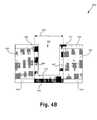
- Structures 250 and 252 in FIGS. 2A and 2Billustrate the result of performing, on a structure including a contact hole formed in a dielectric layer situated over a transistor region of a substrate (not shown in any of the figures) discussed above, steps 150 and 152 of flowchart 100 , respectively.
- barrier layer 202is deposited over dielectric layer 204 , on sidewalls 206 and 207 of contact hole 208 , and over native oxide layer 210 situated at bottom 212 of contact hole 208 and also situated over silicide layer 214 .
- dielectric layer 204is situated over dielectric layer 216 , which is situated over a transistor region of a substrate (not shown in FIG. 2A ).
- Dielectric layer 204can comprise silicon dioxide, which can be deposited, for example, in a plasma enhanced chemical vapor deposition (“PECVD”) process.
- PECVDplasma enhanced chemical vapor deposition
- Native oxide layer 210is situated over silicide layer 214 at bottom 212 of contact hole 208 and can comprise thermally grown oxide.
- native oxide layer 210can have a thickness of between 10.0 Angstroms and 50.0 Angstroms.
- Barrier layer 202can be deposited on sidewalls 206 and 207 of contact hole 208 , over native oxide layer 210 , and over dielectric layer 204 in a manner known in the art and can comprise titanium/titanium nitride (“Ti/TiN”). In other embodiments, barrier layer 202 may comprise a different combination of metals or an appropriate single metal.
- the deposition of barrier layer 202can be optimized such that portions 218 of barrier layer 202 situated adjacent to top corner regions 222 at the top of contact hole 208 have a greater thickness than portion 219 of barrier layer 202 situated at bottom 212 of contact hole 208 .
- portions 218 of barrier layer 202provide sufficient protection for top corner regions 222 of dielectric layer 604 during a subsequent sputter etch process.
- Contact hole width 220which is the distance between sidewall 206 and 207 of contact hole 208 , is also referred to as “electrical contact width” in the present application. Referring to FIG. 2A , the result of step 150 of flowchart 100 is illustrated by structure 250 .
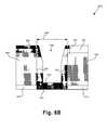
- step 152 of flowchart 100portion 219 of barrier layer 202 and native oxide layer 210 situated at bottom 212 of contact hole 208 are removed to expose silicide layer 214 .
- Portion 219 of barrier layer 202 situated at bottom 212 of contact hole 208 and native oxide layer 210can be removed by utilizing a sputter etch process, which can comprise argon (“Ar”). The sputter etch process also removes portions of barrier layer 202 situated at the top of sidewalls 206 and 207 . However, since portions 218 of barrier layer 202 (shown in FIG.
- step 152 of flowchart 100is illustrated by structure 252 .
- the present inventionavoids etching top corner regions 222 of dielectric layer 204 .
- the present inventionadvantageously achieves a contact having a contact hole width that is not increased during the contact formation process.
- FIG. 3shows a flowchart illustrating an exemplary method for forming a contact over a transistor region of a wafer according to one embodiment of the present invention.
- Certain details and featureshave been left out of flowchart 300 that are apparent to a person of ordinary skill in the art.
- a stepmay consist of one or more substeps or may involve specialized equipment or materials, as known in the art.
- Steps 350 and 352 indicated in flowchart 300are sufficient to describe one embodiment of the present invention, other embodiments of the invention may utilize steps different from those shown in flowchart 300 .
- processing steps shown in flowchart 300are performed on a wafer, which, prior to step 350 , includes a contact hole formed in a dielectric layer and a native oxide layer situated over a silicide layer at the bottom of the contact hole, where the dielectric layer and silicide layer can be situated over a transistor region of a substrate (not shown in any of the figures).
- Structures 350 and 352 in FIGS. 4A and 4Billustrate the result of performing, on a structure including a contact hole formed in a dielectric layer situated over a transistor region of a substrate (not shown in any of the figures) discussed above, steps 350 and 352 of flowchart 300 , respectively.
- step 350 of flowchart 300native oxide layer 410 situated over silicide layer 414 is removed at bottom 412 of contact hole 408 by utilizing reactive hydrogen pre-clean 430 . It is noted that although native oxide layer 410 is removed at step 350 , native oxide layer 410 is shown in FIG. 4A to better illustrate the present embodiment of the invention. In FIG.
- dielectric layers 404 and 416 , sidewalls 406 and 407 , contact hole 408 , native oxide layer 410 , and silicide layer 414 in structure 450correspond, respectively, to dielectric layers 204 and 216 , sidewalls 206 and 207 , contact hole 208 , native oxide layer 210 , and silicide layer 214 in structure 250 in FIG. 2A .
- dielectric layer 404comprises PECVD oxide, which can be hardened in an annealing process after it (i.e. PECVD oxide) has been deposited.
- PECVD oxidei.e. PECVD oxide
- dielectric layer 404is much harder than native oxide layer 410 , which comprises silicon oxide that is thermally grown at room temperature.
- contact hole width 420which is the distance between sidewalls 406 and 407 of contact hole 408 , is not increased after performance of reactive hydrogen pre-clean 430 .
- Contact hole width 420is similar to contact hole width 220 in FIG. 2A and is also referred to as “electrical contact width” in the present application. Referring to FIG. 4A , the result of step 350 of flowchart 300 is illustrated by structure 450 .
- barrier layer 432is deposited on sidewalls 406 and 407 of contact hole 408 , over silicide layer 414 situated at bottom 412 of contact hole 408 , and over dielectric layer 404 .
- Barrier layer 432can be deposited in a manner known in the art and can comprise Ti/TiN. In other embodiments, barrier layer 432 may comprise a different combination of metals or an appropriate single metal.
- Contact hole 408can be filled with a metal such as tungsten in a subsequent step to complete contact formation. Referring to FIG. 4B , the result of step 352 of flowchart 300 is illustrated by structure 452 .
- the present inventionadvantageously provides a contact having a contact hole width that does not increase during contact formation.
- FIG. 5shows a flowchart illustrating an exemplary method for forming a contact over a transistor region of a wafer according to an embodiment of the present invention.
- Certain details and featureshave been left out of flowchart 500 that are apparent to a person of ordinary skill in the art.
- a stepmay consist of one or more substeps or may involve specialized equipment or materials, as known in the art.
- Steps 550 and 552 indicated in flowchart 500are sufficient to describe one embodiment of the present invention, other embodiments of the invention may utilize steps different from those shown in flowchart 500 .
- processing steps shown in flowchart 500are performed on a wafer, which, prior to step 550 , includes a contact hole formed in a dielectric layer and a native oxide layer situated over a silicide layer at the bottom of the contact hole, where the dielectric layer and silicide layer can be situated over a transistor region of a substrate (not shown in any of the figures).
- Structures 550 and 552 in FIGS. 6A and 6Billustrate the result of performing, on a structure including a contact hole formed in a dielectric layer situated over a transistor region of a substrate (not shown in any of the figures) discussed above, steps 550 and 552 of flowchart 500 , respectively.
- barrier layer 602is deposited on sidewalls 606 and 607 of contact hole 608 , over native oxide layer 610 situated at bottom 612 of contact hole 608 , and over dielectric layer 604 , which is situated over dielectric layer 616 .
- Step 550 in FIG. 5corresponds to step 350 in FIG. 3 .
- barrier layer 602 , dielectric layers 604 and 616 , sidewalls 606 and 607 , contact hole 608 , native oxide layer 610 , bottom 612 , silicide layer 614 , portions 618 , portion 619 , contact hole width 620 , and top corner regions 622 in structure 650 in FIG. 6Acorrespond, respectively, to barrier layer 202 , dielectric layers 204 and 216 , sidewalls 206 and 207 , contact hole 208 , native oxide layer 210 , bottom 212 , silicide layer 214 , portions 218 , portion 219 , contact hole width 220 , and top corner regions 222 in structure 250 in FIG. 2A .
- contact hole width 420is also referred to as “electrical contact width” in the present application. Similar to barrier layer 202 in FIG. 2A , the deposition of barrier layer 602 can be optimized in the present embodiment such that portions 618 of barrier layer 602 situated adjacent to top corner portions 222 at the top of contact hole 608 have a greater thickness than portion 619 of barrier layer 602 situated at bottom 612 of contact hole 608 . Referring to FIG. 6A , the result of step 550 of flowchart 500 is illustrated by structure 650 .
- a simultaneous sputter etch/deposition processis performed to remove native oxide layer 610 situated over silicide layer 614 at bottom 612 of contact hole 608 .
- Arcan be utilized for sputter etching and Ti/TiN can be deposited on sidewalls 606 and bottom 612 of contact hole 608 , utilizing, for example, a sputter deposition technique.
- the simultaneous sputter etch/deposition processcan utilize an appropriate sputter etch/deposition ratio such that native oxide layer 610 is etched (i.e. removed).
- the ratio of Ar and Ti/TiN moleculescan be selected to achieve a sputter etch/deposition ratio of between 1.0 and 2.0.
- a sputter etch/deposition ratio greater than 1.0the present embodiment achieves removal of native oxide layer 610 while protecting top corner regions 622 of dielectric layer 604 by depositing Ti/TiN back onto sidewalls 606 and 607 of contact hole 608 .
- Contact hole 608can be filled with a metal such as tungsten in a subsequent step to complete contact formation. Referring to FIG. 6B , the result of step 552 of flowchart 500 is illustrated by structure 652 .
- the present inventionachieves removal of a native oxide layer at the bottom of a contact hole situated over a silicide layer while preventing an undesirable increase in contact hole width during contact formation.
- the present inventionachieves removal of a native oxide layer at the bottom of a contact hole while preventing an undesirable increase in contact hole width during contact formation.
- a conventional contact formation processwhich utilizes an Ar sputter etch to remove a native oxide layer prior to barrier layer deposition, results in an undesirable increase in contact hole width.
Landscapes
- Engineering & Computer Science (AREA)
- Physics & Mathematics (AREA)
- Condensed Matter Physics & Semiconductors (AREA)
- General Physics & Mathematics (AREA)
- Manufacturing & Machinery (AREA)
- Computer Hardware Design (AREA)
- Microelectronics & Electronic Packaging (AREA)
- Power Engineering (AREA)
- Internal Circuitry In Semiconductor Integrated Circuit Devices (AREA)
- Electrodes Of Semiconductors (AREA)
Abstract
Description
- The present invention is generally in the field of semiconductor device fabrication. More particularly, the present invention is in the field of contact formation for semiconductor devices in a semiconductor die.
- Contacts are utilized, among other things, to provide connections between a transistor region of a semiconductor die and an interconnect metal layer situated above the transistor region. To achieve high circuit density, these contacts, which generally have a high aspect ratio, must fit within a small area of the semiconductor die without touching or otherwise interfering with each other. As such, it is important to control contact hole width during contact formation to achieve a contact having a sufficiently small width.
- During a conventional contact fabrication process, a contact hole is typically defined by lithography and etched in an oxide layer, which can be situated, for example, over a transistor region of a semiconductor die. The resulting contact hole can be formed over a silicide layer, which can be connected to, for example, a source or drain area in the transistor region of the semiconductor die. The contact hole is then lined with a barrier layer comprising a metal, such as titanium, and filled with a metal, such as tungsten, to form a contact. However, before the barrier layer can be deposited on the sidewalls of the contact hole and on the silicide layer situated at the bottom of contact hole, a native oxide layer that forms over the silicide layer must first be removed. In the conventional contact fabrication process, the native oxide layer is typically removed by utilizing a sputter etch process comprising argon.
- However, during the sputter etch process, top corner portions of the oxide layer than defines the contact hole are also etched in addition to the native oxide layer, which causes the top of the contact hole to increase in width. As a result, the contact that is formed after the contact hole has been filled with tungsten has an undesirable increased width compared to the initial width of the patterned contact hole.
- Thus, there is a need in the art for a method for forming a contact over a transistor region of a semiconductor die that prevents an undesirable increase in contact hole width during contact formation.
- The present invention is directed to method for preventing an increase in contact hole width during contact formation. The present invention addresses and resolves the need in the art for a method for forming a contact over a transistor region of a semiconductor die that prevents an undesirable increase in contact hole width during contact formation.
- According to one exemplary embodiment, a method for forming a contact over a silicide layer situated in a semiconductor die comprises a step of depositing a barrier layer on sidewalls of a contact hole and on a native oxide layer situated at a bottom of the contact hole, where the sidewalls are defined by the contact hole in a dielectric layer. For example, the barrier layer may be titanium/titanium nitride and dielectric layer may be PECVD oxide. The step of depositing the barrier layer on the sidewalls of the contact hole and on the native oxide layer can be optimized such that the barrier layer has a greater thickness at a top of the contact hole than a thickness at the bottom of the contact hole.
- According to this exemplary embodiment, the method further comprises a step of removing a portion of the barrier layer and the native oxide layer situated at the bottom of the contact hole to expose the silicide layer. For example, the portion of the barrier layer and the native oxide layer situated at the bottom of the contact hole can be removed by utilizing a sputter etch process. The contact hole comprises an electrical contact width, where the electrical contact width is not increased by the sputter etch process. The dielectric layer comprises top corner regions situated adjacent to the contact hole, where the top corner regions of the dielectric layer are not etch during the step of removing the portion of the barrier layer and the native oxide layer situated at the bottom of the contact hole. Other features and advantages of the present invention will become more readily apparent to those of ordinary skill in the art after reviewing the following detailed description and accompanying drawings.
FIG. 1 is a flowchart corresponding to exemplary method steps according to one embodiment of the present invention.FIG. 2A illustrates a cross-sectional view of a portion of a wafer processed according to an embodiment of the invention, corresponding to certain steps of the flowchart inFIG. 1 .FIG. 2B illustrates a cross-sectional view of a portion of a wafer processed according to an embodiment of the invention, corresponding to certain steps of the flowchart inFIG. 1 .FIG. 3 is a flowchart corresponding to exemplary method steps according to one embodiment of the present invention.FIG. 4A illustrates a cross-sectional view of a portion of a wafer processed according to an embodiment of the invention, corresponding to certain steps of the flowchart inFIG. 3 .FIG. 4B illustrates a cross-sectional view of a portion of a wafer processed according to an embodiment of the invention, corresponding to certain steps of the flowchart inFIG. 3 .FIG. 5 is a flowchart corresponding to exemplary method steps according to one embodiment of the present invention.FIG. 6A illustrates a cross-sectional view of a portion of a wafer processed according to an embodiment of the invention, corresponding to certain steps of the flowchart inFIG. 5 .FIG. 6B illustrates a cross-sectional view of a portion of a wafer processed according to an embodiment of the invention, corresponding to certain steps of the flowchart inFIG. 5 .- The present invention is directed to method for preventing increased contact hole width during contact formation in a semiconductor die. The following description contains specific information pertaining to the implementation of the present invention. One skilled in the art will recognize that the present invention may be implemented in a manner different from that specifically discussed in the present application. Moreover, some of the specific details of the invention are not discussed in order not to obscure the invention.
- The drawings in the present application and their accompanying detailed description are directed to merely exemplary embodiments of the invention. To maintain brevity, other embodiments of the present invention are not specifically described in the present application and are not specifically illustrated by the present drawings.
FIG. 1 shows a flowchart illustrating an exemplary method for forming a contact over a transistor region in a semiconductor die according to one embodiment of the present invention. Certain details and features have been left out offlowchart 100 that are apparent to a person of ordinary skill in the art. For example, a step may consist of one or more substeps or may involve specialized equipment or materials, as known in the art.Steps flowchart 100 are sufficient to describe one embodiment of the present invention, other embodiments of the invention may utilize steps different from those shown inflowchart 100. It is noted that the processing steps shown inflowchart 100 are performed on a wafer, which, prior tostep 150, includes a contact hole formed in a dielectric layer and a native oxide layer situated over a silicide layer at the bottom of the contact hole, where the dielectric layer and silicide layer can be situated over a transistor region of a substrate (not shown in any of the figures).Structures FIGS. 2A and 2B illustrate the result of performing, on a structure including a contact hole formed in a dielectric layer situated over a transistor region of a substrate (not shown in any of the figures) discussed above,steps flowchart 100, respectively.- Referring now to
step 150 inFIG. 1 andstructure 250 inFIG. 2A , atstep 150 offlowchart 100,barrier layer 202 is deposited overdielectric layer 204, onsidewalls contact hole 208, and overnative oxide layer 210 situated atbottom 212 ofcontact hole 208 and also situated oversilicide layer 214. As shown inFIG. 2A ,dielectric layer 204 is situated overdielectric layer 216, which is situated over a transistor region of a substrate (not shown inFIG. 2A ).Dielectric layer 204 can comprise silicon dioxide, which can be deposited, for example, in a plasma enhanced chemical vapor deposition (“PECVD”) process. Silicon dioxide deposited in a PECVD process is also referred to as “PECVD oxide” in the present application.Native oxide layer 210 is situated oversilicide layer 214 atbottom 212 ofcontact hole 208 and can comprise thermally grown oxide. By way of example,native oxide layer 210 can have a thickness of between 10.0 Angstroms and 50.0 Angstroms.Barrier layer 202 can be deposited onsidewalls contact hole 208, overnative oxide layer 210, and overdielectric layer 204 in a manner known in the art and can comprise titanium/titanium nitride (“Ti/TiN”). In other embodiments,barrier layer 202 may comprise a different combination of metals or an appropriate single metal. In the present embodiment, the deposition ofbarrier layer 202 can be optimized such thatportions 218 ofbarrier layer 202 situated adjacent totop corner regions 222 at the top ofcontact hole 208 have a greater thickness thanportion 219 ofbarrier layer 202 situated atbottom 212 ofcontact hole 208. As a result,portions 218 ofbarrier layer 202 provide sufficient protection fortop corner regions 222 ofdielectric layer 604 during a subsequent sputter etch process.Contact hole width 220, which is the distance betweensidewall contact hole 208, is also referred to as “electrical contact width” in the present application. Referring toFIG. 2A , the result ofstep 150 offlowchart 100 is illustrated bystructure 250. - Continuing with
step 152 inFIG. 1 andstructure 252 inFIG. 2B , atstep 152 offlowchart 100,portion 219 ofbarrier layer 202 andnative oxide layer 210 situated atbottom 212 ofcontact hole 208 are removed to exposesilicide layer 214.Portion 219 ofbarrier layer 202 situated atbottom 212 ofcontact hole 208 andnative oxide layer 210 can be removed by utilizing a sputter etch process, which can comprise argon (“Ar”). The sputter etch process also removes portions ofbarrier layer 202 situated at the top ofsidewalls portions 218 of barrier layer202 (shown inFIG. 2A ) have sufficient thickness to protecttop corner regions 222 ofdielectric layer 204,top corner regions 222 are not etched during the sputter etch process. As a result,contact hole width 220 is not increased during the sputter etch process.Contact hole 208 can be filled with a metal such as tungsten in a subsequent step to complete contact formation. Referring toFIG. 2B , the result ofstep 152 offlowchart 100 is illustrated bystructure 252. - Thus, in the embodiment of the present invention in
FIG. 1 , by formingbarrier layer 202 prior to performing a sputter etch process to removenative oxide layer 210 and optimizing the formation ofbarrier layer 202, the present invention avoids etchingtop corner regions 222 ofdielectric layer 204. As a result, the present invention advantageously achieves a contact having a contact hole width that is not increased during the contact formation process. FIG. 3 shows a flowchart illustrating an exemplary method for forming a contact over a transistor region of a wafer according to one embodiment of the present invention. Certain details and features have been left out offlowchart 300 that are apparent to a person of ordinary skill in the art. For example, a step may consist of one or more substeps or may involve specialized equipment or materials, as known in the art.Steps flowchart 300 are sufficient to describe one embodiment of the present invention, other embodiments of the invention may utilize steps different from those shown inflowchart 300. It is noted that the processing steps shown inflowchart 300 are performed on a wafer, which, prior to step350, includes a contact hole formed in a dielectric layer and a native oxide layer situated over a silicide layer at the bottom of the contact hole, where the dielectric layer and silicide layer can be situated over a transistor region of a substrate (not shown in any of the figures).Structures FIGS. 4A and 4B illustrate the result of performing, on a structure including a contact hole formed in a dielectric layer situated over a transistor region of a substrate (not shown in any of the figures) discussed above, steps350 and352 offlowchart 300, respectively.- Referring now to step350 in
FIG. 3 andstructure 450 inFIG. 4A , atstep 350 offlowchart 300,native oxide layer 410 situated oversilicide layer 414 is removed atbottom 412 ofcontact hole 408 by utilizingreactive hydrogen pre-clean 430. It is noted that althoughnative oxide layer 410 is removed atstep 350,native oxide layer 410 is shown inFIG. 4A to better illustrate the present embodiment of the invention. InFIG. 4A ,dielectric layers sidewalls contact hole 408,native oxide layer 410, andsilicide layer 414 instructure 450 correspond, respectively, todielectric layers sidewalls contact hole 208,native oxide layer 210, andsilicide layer 214 instructure 250 inFIG. 2A . In the present embodiment,dielectric layer 404 comprises PECVD oxide, which can be hardened in an annealing process after it (i.e. PECVD oxide) has been deposited. Thus,dielectric layer 404 is much harder thannative oxide layer 410, which comprises silicon oxide that is thermally grown at room temperature. As a result, whennative oxide layer 410 is etched away (i.e. removed) by the reactive hydrogen pre-clean, i.e.reactive hydrogen pre-clean 430,top corner regions 422 ofdielectric layer 404, which are situated at the tops ofsidewalls 406, are not etched. Thus,contact hole width 420, which is the distance betweensidewalls contact hole 408, is not increased after performance ofreactive hydrogen pre-clean 430.Contact hole width 420 is similar to contacthole width 220 inFIG. 2A and is also referred to as “electrical contact width” in the present application. Referring toFIG. 4A , the result ofstep 350 offlowchart 300 is illustrated bystructure 450. - Continuing with
step 352 inFIG. 3 andstructure 452 inFIG. 4B , atstep 352 offlowchart 300,barrier layer 432 is deposited onsidewalls contact hole 408, oversilicide layer 414 situated atbottom 412 ofcontact hole 408, and overdielectric layer 404.Barrier layer 432 can be deposited in a manner known in the art and can comprise Ti/TiN. In other embodiments,barrier layer 432 may comprise a different combination of metals or an appropriate single metal.Contact hole 408 can be filled with a metal such as tungsten in a subsequent step to complete contact formation. Referring toFIG. 4B , the result ofstep 352 offlowchart 300 is illustrated bystructure 452. - Thus, in the embodiment of the present invention in
FIG. 3 , by utilizing a reactive hydrogen pre-clean process to remove a native oxide layer at the bottom of a contact hole prior to depositing a barrier layer in the contact hole, the present invention advantageously provides a contact having a contact hole width that does not increase during contact formation. FIG. 5 shows a flowchart illustrating an exemplary method for forming a contact over a transistor region of a wafer according to an embodiment of the present invention. Certain details and features have been left out offlowchart 500 that are apparent to a person of ordinary skill in the art. For example, a step may consist of one or more substeps or may involve specialized equipment or materials, as known in the art.Steps flowchart 500 are sufficient to describe one embodiment of the present invention, other embodiments of the invention may utilize steps different from those shown inflowchart 500. It is noted that the processing steps shown inflowchart 500 are performed on a wafer, which, prior to step550, includes a contact hole formed in a dielectric layer and a native oxide layer situated over a silicide layer at the bottom of the contact hole, where the dielectric layer and silicide layer can be situated over a transistor region of a substrate (not shown in any of the figures).Structures FIGS. 6A and 6B illustrate the result of performing, on a structure including a contact hole formed in a dielectric layer situated over a transistor region of a substrate (not shown in any of the figures) discussed above, steps550 and552 offlowchart 500, respectively.- Referring now to step550 in
FIG. 5 andstructure 450 inFIG. 4A , atstep 550 offlowchart 500,barrier layer 602 is deposited onsidewalls contact hole 608, overnative oxide layer 610 situated atbottom 612 ofcontact hole 608, and overdielectric layer 604, which is situated overdielectric layer 616. Step550 inFIG. 5 corresponds to step350 inFIG. 3 . In particular,barrier layer 602,dielectric layers sidewalls contact hole 608,native oxide layer 610, bottom612,silicide layer 614,portions 618,portion 619,contact hole width 620, andtop corner regions 622 instructure 650 inFIG. 6A correspond, respectively, tobarrier layer 202,dielectric layers sidewalls contact hole 208,native oxide layer 210, bottom212,silicide layer 214,portions 218,portion 219,contact hole width 220, andtop corner regions 222 instructure 250 inFIG. 2A . Thus, similar to contacthole width 220 inFIG. 2A ,contact hole width 420 is also referred to as “electrical contact width” in the present application. Similar tobarrier layer 202 inFIG. 2A , the deposition ofbarrier layer 602 can be optimized in the present embodiment such thatportions 618 ofbarrier layer 602 situated adjacent totop corner portions 222 at the top ofcontact hole 608 have a greater thickness thanportion 619 ofbarrier layer 602 situated atbottom 612 ofcontact hole 608. Referring toFIG. 6A , the result ofstep 550 offlowchart 500 is illustrated bystructure 650. - Continuing with
step 552 inFIG. 5 andstructure 652 inFIG. 6B , atstep 552 offlowchart 500, a simultaneous sputter etch/deposition process is performed to removenative oxide layer 610 situated oversilicide layer 614 atbottom 612 ofcontact hole 608. In the simultaneous sputter etch/deposition process, Ar can be utilized for sputter etching and Ti/TiN can be deposited onsidewalls 606 andbottom 612 ofcontact hole 608, utilizing, for example, a sputter deposition technique. The simultaneous sputter etch/deposition process can utilize an appropriate sputter etch/deposition ratio such thatnative oxide layer 610 is etched (i.e. removed). By way of example, the ratio of Ar and Ti/TiN molecules can be selected to achieve a sputter etch/deposition ratio of between 1.0 and 2.0. Thus, by utilizing a sputter etch/deposition ratio greater than 1.0, the present embodiment achieves removal ofnative oxide layer 610 while protectingtop corner regions 622 ofdielectric layer 604 by depositing Ti/TiN back ontosidewalls contact hole 608.Contact hole 608 can be filled with a metal such as tungsten in a subsequent step to complete contact formation. Referring toFIG. 6B , the result ofstep 552 offlowchart 500 is illustrated bystructure 652. - Thus, in the embodiment of the present invention in
FIG. 5 , by utilizing a simultaneous sputter etch/deposition process, the present invention achieves removal of a native oxide layer at the bottom of a contact hole situated over a silicide layer while preventing an undesirable increase in contact hole width during contact formation. - Thus, as discussed above, in embodiments of the invention in
FIGS. 1, 3 , and5, by appropriately selecting the sequence and techniques for sputter etch and barrier layer deposition processes, the present invention achieves removal of a native oxide layer at the bottom of a contact hole while preventing an undesirable increase in contact hole width during contact formation. In contrast, a conventional contact formation process, which utilizes an Ar sputter etch to remove a native oxide layer prior to barrier layer deposition, results in an undesirable increase in contact hole width. - From the above description of exemplary embodiments of the invention it is manifest that various techniques can be used for implementing the concepts of the present invention without departing from its scope. Moreover, while the invention has been described with specific reference to certain embodiments, a person of ordinary skill in the art would recognize that changes could be made in form and detail without departing from the spirit and the scope of the invention. The described exemplary embodiments are to be considered in all respects as illustrative and not restrictive. It should also be understood that the invention is not limited to the particular exemplary embodiments described herein, but is capable of many rearrangements, modifications, and substitutions without departing from the scope of the invention.
- Thus, method for preventing an increase in contact hole width during contact formation has been described.
Claims (20)
Priority Applications (8)
| Application Number | Priority Date | Filing Date | Title |
|---|---|---|---|
| US10/705,631US7005387B2 (en) | 2003-11-08 | 2003-11-08 | Method for preventing an increase in contact hole width during contact formation |
| PCT/US2004/033417WO2005048342A1 (en) | 2003-11-08 | 2004-10-08 | Method for preventing an increase in contact hole width during contact formation |
| DE112004002156TDE112004002156T5 (en) | 2003-11-08 | 2004-10-08 | A method of preventing the increase in contact hole width during contact making |
| KR1020067008659AKR101180977B1 (en) | 2003-11-08 | 2004-10-08 | Method for preventing an increase in contact hole width during contact formation |
| CNA2004800337772ACN1883045A (en) | 2003-11-08 | 2004-10-08 | Method for preventing an increase in contact hole width during contact formation |
| JP2006539499AJP4662943B2 (en) | 2003-11-08 | 2004-10-08 | How to prevent an increase in contact hole width during contact formation |
| GB0608285AGB2423635B (en) | 2003-11-08 | 2004-10-08 | Method for preventing an increase in contact hole width during contact formation |
| TW093131505ATWI359475B (en) | 2003-11-08 | 2004-10-18 | Method for preventing an increase in contact hole |
Applications Claiming Priority (1)
| Application Number | Priority Date | Filing Date | Title |
|---|---|---|---|
| US10/705,631US7005387B2 (en) | 2003-11-08 | 2003-11-08 | Method for preventing an increase in contact hole width during contact formation |
Publications (2)
| Publication Number | Publication Date |
|---|---|
| US20050101148A1true US20050101148A1 (en) | 2005-05-12 |
| US7005387B2 US7005387B2 (en) | 2006-02-28 |
Family
ID=34552414
Family Applications (1)
| Application Number | Title | Priority Date | Filing Date |
|---|---|---|---|
| US10/705,631Expired - Fee RelatedUS7005387B2 (en) | 2003-11-08 | 2003-11-08 | Method for preventing an increase in contact hole width during contact formation |
Country Status (8)
| Country | Link |
|---|---|
| US (1) | US7005387B2 (en) |
| JP (1) | JP4662943B2 (en) |
| KR (1) | KR101180977B1 (en) |
| CN (1) | CN1883045A (en) |
| DE (1) | DE112004002156T5 (en) |
| GB (1) | GB2423635B (en) |
| TW (1) | TWI359475B (en) |
| WO (1) | WO2005048342A1 (en) |
Cited By (3)
| Publication number | Priority date | Publication date | Assignee | Title |
|---|---|---|---|---|
| US20080038910A1 (en)* | 2006-08-10 | 2008-02-14 | Advanced Micro Devices, Inc. | Multiple lithography for reduced negative feature corner rounding |
| US20090050471A1 (en)* | 2007-08-24 | 2009-02-26 | Spansion Llc | Process of forming an electronic device including depositing layers within openings |
| CN110718501A (en)* | 2018-07-13 | 2020-01-21 | 爱思开海力士有限公司 | Gap filling method and method for manufacturing semiconductor device using the same |
Families Citing this family (3)
| Publication number | Priority date | Publication date | Assignee | Title |
|---|---|---|---|---|
| JP6494940B2 (en)* | 2013-07-25 | 2019-04-03 | ラム リサーチ コーポレーションLam Research Corporation | Void-free tungsten filling to different size features |
| US9972504B2 (en) | 2015-08-07 | 2018-05-15 | Lam Research Corporation | Atomic layer etching of tungsten for enhanced tungsten deposition fill |
| WO2024147230A1 (en) | 2023-01-05 | 2024-07-11 | 富士電機株式会社 | Semiconductor device, and manufacturing method for same |
Citations (10)
| Publication number | Priority date | Publication date | Assignee | Title |
|---|---|---|---|---|
| US6010958A (en)* | 1997-05-20 | 2000-01-04 | United Microelectronics Corp. | Method for improving the planarization of dielectric layer in the fabrication of metallic interconnects |
| US6204550B1 (en)* | 1997-11-21 | 2001-03-20 | Lsi Logic Corporation | Method and composition for reducing gate oxide damage during RF sputter clean |
| US20010012695A1 (en)* | 2000-02-08 | 2001-08-09 | Won-Hwa Jin | Bit line and manufacturing method thereof |
| US6303505B1 (en)* | 1998-07-09 | 2001-10-16 | Advanced Micro Devices, Inc. | Copper interconnect with improved electromigration resistance |
| US20020045355A1 (en)* | 2000-01-29 | 2002-04-18 | Samsung Electronics Co., Ltd. | Method of manufacturing a semiconductor device having a silicide layer |
| US6452273B1 (en)* | 1999-01-02 | 2002-09-17 | Samsung Electronics Co., Ltd. | Semiconductor integrated circuit device and method of manufacturing the same |
| US6498091B1 (en)* | 2000-11-01 | 2002-12-24 | Applied Materials, Inc. | Method of using a barrier sputter reactor to remove an underlying barrier layer |
| US6511575B1 (en)* | 1998-11-12 | 2003-01-28 | Canon Kabushiki Kaisha | Treatment apparatus and method utilizing negative hydrogen ion |
| US20030073304A1 (en)* | 2001-10-16 | 2003-04-17 | Applied Materials, Inc. | Selective tungsten stud as copper diffusion barrier to silicon contact |
| US6806187B2 (en)* | 1999-03-15 | 2004-10-19 | Micron Technology, Inc. | Electrical contact for high dielectric constant capacitors and method for fabricating the same |
Family Cites Families (11)
| Publication number | Priority date | Publication date | Assignee | Title |
|---|---|---|---|---|
| JPH0513411A (en)* | 1991-07-02 | 1993-01-22 | Nec Corp | Manufacture of semiconductor device |
| JPH0661181A (en) | 1992-08-11 | 1994-03-04 | Sony Corp | Method of forming barrier metal |
| JP3237917B2 (en)* | 1992-09-22 | 2001-12-10 | 沖電気工業株式会社 | Method for manufacturing semiconductor device |
| JPH06349824A (en)* | 1993-06-10 | 1994-12-22 | Toshiba Corp | Manufacture of semiconductor device |
| JPH09116009A (en)* | 1995-10-23 | 1997-05-02 | Sony Corp | Forming method for connecting hole |
| JPH09139358A (en)* | 1995-11-13 | 1997-05-27 | Sony Corp | Method for manufacturing semiconductor device |
| US5985762A (en)* | 1997-05-19 | 1999-11-16 | International Business Machines Corporation | Method of forming a self-aligned copper diffusion barrier in vias |
| JP3201318B2 (en)* | 1997-11-05 | 2001-08-20 | 日本電気株式会社 | Method for manufacturing semiconductor device |
| JP4221859B2 (en)* | 1999-02-12 | 2009-02-12 | 株式会社デンソー | Manufacturing method of semiconductor device |
| JP2000323571A (en)* | 1999-05-14 | 2000-11-24 | Sony Corp | Manufacture of semiconductor device |
| US6624066B2 (en) | 2001-02-14 | 2003-09-23 | Texas Instruments Incorporated | Reliable interconnects with low via/contact resistance |
- 2003
- 2003-11-08USUS10/705,631patent/US7005387B2/ennot_activeExpired - Fee Related
- 2004
- 2004-10-08KRKR1020067008659Apatent/KR101180977B1/ennot_activeExpired - Fee Related
- 2004-10-08GBGB0608285Apatent/GB2423635B/ennot_activeExpired - Fee Related
- 2004-10-08CNCNA2004800337772Apatent/CN1883045A/enactivePending
- 2004-10-08JPJP2006539499Apatent/JP4662943B2/ennot_activeExpired - Fee Related
- 2004-10-08DEDE112004002156Tpatent/DE112004002156T5/ennot_activeCeased
- 2004-10-08WOPCT/US2004/033417patent/WO2005048342A1/enactiveApplication Filing
- 2004-10-18TWTW093131505Apatent/TWI359475B/ennot_activeIP Right Cessation
Patent Citations (10)
| Publication number | Priority date | Publication date | Assignee | Title |
|---|---|---|---|---|
| US6010958A (en)* | 1997-05-20 | 2000-01-04 | United Microelectronics Corp. | Method for improving the planarization of dielectric layer in the fabrication of metallic interconnects |
| US6204550B1 (en)* | 1997-11-21 | 2001-03-20 | Lsi Logic Corporation | Method and composition for reducing gate oxide damage during RF sputter clean |
| US6303505B1 (en)* | 1998-07-09 | 2001-10-16 | Advanced Micro Devices, Inc. | Copper interconnect with improved electromigration resistance |
| US6511575B1 (en)* | 1998-11-12 | 2003-01-28 | Canon Kabushiki Kaisha | Treatment apparatus and method utilizing negative hydrogen ion |
| US6452273B1 (en)* | 1999-01-02 | 2002-09-17 | Samsung Electronics Co., Ltd. | Semiconductor integrated circuit device and method of manufacturing the same |
| US6806187B2 (en)* | 1999-03-15 | 2004-10-19 | Micron Technology, Inc. | Electrical contact for high dielectric constant capacitors and method for fabricating the same |
| US20020045355A1 (en)* | 2000-01-29 | 2002-04-18 | Samsung Electronics Co., Ltd. | Method of manufacturing a semiconductor device having a silicide layer |
| US20010012695A1 (en)* | 2000-02-08 | 2001-08-09 | Won-Hwa Jin | Bit line and manufacturing method thereof |
| US6498091B1 (en)* | 2000-11-01 | 2002-12-24 | Applied Materials, Inc. | Method of using a barrier sputter reactor to remove an underlying barrier layer |
| US20030073304A1 (en)* | 2001-10-16 | 2003-04-17 | Applied Materials, Inc. | Selective tungsten stud as copper diffusion barrier to silicon contact |
Cited By (4)
| Publication number | Priority date | Publication date | Assignee | Title |
|---|---|---|---|---|
| US20080038910A1 (en)* | 2006-08-10 | 2008-02-14 | Advanced Micro Devices, Inc. | Multiple lithography for reduced negative feature corner rounding |
| US20090050471A1 (en)* | 2007-08-24 | 2009-02-26 | Spansion Llc | Process of forming an electronic device including depositing layers within openings |
| WO2009029431A1 (en)* | 2007-08-24 | 2009-03-05 | Spansion Llc | Process of forming an electronic device including depositing layers within openings |
| CN110718501A (en)* | 2018-07-13 | 2020-01-21 | 爱思开海力士有限公司 | Gap filling method and method for manufacturing semiconductor device using the same |
Also Published As
| Publication number | Publication date |
|---|---|
| JP4662943B2 (en) | 2011-03-30 |
| KR101180977B1 (en) | 2012-09-07 |
| GB0608285D0 (en) | 2006-06-07 |
| GB2423635A (en) | 2006-08-30 |
| JP2007511087A (en) | 2007-04-26 |
| TWI359475B (en) | 2012-03-01 |
| DE112004002156T5 (en) | 2006-09-14 |
| CN1883045A (en) | 2006-12-20 |
| GB2423635B (en) | 2007-05-30 |
| KR20060107763A (en) | 2006-10-16 |
| TW200524077A (en) | 2005-07-16 |
| WO2005048342A1 (en) | 2005-05-26 |
| US7005387B2 (en) | 2006-02-28 |
Similar Documents
| Publication | Publication Date | Title |
|---|---|---|
| US8877651B2 (en) | Semiconductor device and manufacturing method involving multilayer contact etch stop | |
| US6468904B1 (en) | RPO process for selective CoSix formation | |
| JP4587774B2 (en) | Method for forming a semiconductor device | |
| US6107171A (en) | Method to manufacture metal gate of integrated circuits | |
| KR100871920B1 (en) | Semiconductor device and manufacturing method thereof | |
| US20070066047A1 (en) | Method of forming opening and contact | |
| US20030203615A1 (en) | Method for depositing barrier layers in an opening | |
| US7005387B2 (en) | Method for preventing an increase in contact hole width during contact formation | |
| US7067417B2 (en) | Methods of removing resistive remnants from contact holes using silicidation | |
| US6372640B1 (en) | Method of locally forming metal silicide layers | |
| US9449922B2 (en) | Contact critical dimension control | |
| US8003528B2 (en) | Semiconductor structure and method for making the same | |
| KR100503312B1 (en) | Method for manufacturing a contact electrode of semiconductor device | |
| US6706596B2 (en) | Method for forming flash memory cell | |
| US20080070417A1 (en) | Method of etching semiconductor device and method of fabricating semiconductor device using the same | |
| KR100634258B1 (en) | Manufacturing Method of Semiconductor Device | |
| KR100370143B1 (en) | Method for forming contact plug of Semiconductor device | |
| US7700451B2 (en) | Method of manufacturing a transistor | |
| KR100714039B1 (en) | Method for fabrication a semiconductor device | |
| KR100642917B1 (en) | Metal wiring formation method of semiconductor device | |
| US20110223768A1 (en) | Method for Forming Contact Opening | |
| KR100755053B1 (en) | Bit line formation method of semiconductor device | |
| US20200043737A1 (en) | Method for silicidation of semiconductor device, and corresponding semiconductor device | |
| JP2006203109A (en) | Semiconductor device and manufacturing method thereof | |
| KR0167238B1 (en) | Wiring Manufacturing Method of Semiconductor Device |
Legal Events
| Date | Code | Title | Description |
|---|---|---|---|
| AS | Assignment | Owner name:ADVANCED MICRO DEVICES, INC., CALIFORNIA Free format text:ASSIGNMENT OF ASSIGNORS INTEREST;ASSIGNORS:HOPPER DAWN;KINOSHITA, HIROYUKI;WOO, CHRISTY;REEL/FRAME:014697/0055 Effective date:20031020 | |
| FPAY | Fee payment | Year of fee payment:4 | |
| AS | Assignment | Owner name:GLOBALFOUNDRIES INC., CAYMAN ISLANDS Free format text:AFFIRMATION OF PATENT ASSIGNMENT;ASSIGNOR:ADVANCED MICRO DEVICES, INC.;REEL/FRAME:023119/0083 Effective date:20090630 | |
| FPAY | Fee payment | Year of fee payment:8 | |
| FEPP | Fee payment procedure | Free format text:MAINTENANCE FEE REMINDER MAILED (ORIGINAL EVENT CODE: REM.) | |
| LAPS | Lapse for failure to pay maintenance fees | Free format text:PATENT EXPIRED FOR FAILURE TO PAY MAINTENANCE FEES (ORIGINAL EVENT CODE: EXP.) | |
| STCH | Information on status: patent discontinuation | Free format text:PATENT EXPIRED DUE TO NONPAYMENT OF MAINTENANCE FEES UNDER 37 CFR 1.362 | |
| FP | Lapsed due to failure to pay maintenance fee | Effective date:20180228 | |
| AS | Assignment | Owner name:GLOBALFOUNDRIES U.S. INC., NEW YORK Free format text:RELEASE BY SECURED PARTY;ASSIGNOR:WILMINGTON TRUST, NATIONAL ASSOCIATION;REEL/FRAME:056987/0001 Effective date:20201117 |