US20050097488A1 - Method of partitioning an integrated circuit design for physical design verification - Google Patents
Method of partitioning an integrated circuit design for physical design verificationDownload PDFInfo
- Publication number
- US20050097488A1 US20050097488A1US10/697,357US69735703AUS2005097488A1US 20050097488 A1US20050097488 A1US 20050097488A1US 69735703 AUS69735703 AUS 69735703AUS 2005097488 A1US2005097488 A1US 2005097488A1
- Authority
- US
- United States
- Prior art keywords
- run
- decks
- deck
- partitioned
- physical design
- Prior art date
- Legal status (The legal status is an assumption and is not a legal conclusion. Google has not performed a legal analysis and makes no representation as to the accuracy of the status listed.)
- Granted
Links
Images


Classifications
- G—PHYSICS
- G06—COMPUTING OR CALCULATING; COUNTING
- G06F—ELECTRIC DIGITAL DATA PROCESSING
- G06F30/00—Computer-aided design [CAD]
- G06F30/30—Circuit design
- G06F30/39—Circuit design at the physical level
- G06F30/398—Design verification or optimisation, e.g. using design rule check [DRC], layout versus schematics [LVS] or finite element methods [FEM]
Definitions
- the present inventionrelates generally to the design of integrated circuits. More specifically, but without limitation thereto, the present invention relates to methods of partitioning an integrated circuit design into a smaller address space to increase efficiency of physical design verification tools.
- Physical design verification toolsare typically run on 32-bit processors and 64-bit processors to verify integrated circuit designs represented by GDS2 files.
- the 32-bit processorshave an address space that can accommodate integrated circuit designs up to 3.5 gigabytes in size, while the 64-bit processors have a larger address space that affords the capability of accommodating integrated designs larger than 3.5 gigabytes.
- a method of partitioning an integrated circuit design for physical design verificationincludes steps of:
- a computer program product for partitioning an integrated circuit design for physical design verificationincludes:
- FIG. 1illustrates a flow diagram of a typical physical design verification process of the prior art
- FIG. 2illustrates a flow diagram of a physical design verification process according to an embodiment of the present invention.
- FIG. 3illustrates a flow chart of a method of partitioning an integrated circuit design for physical design verification according to an embodiment of the present invention.
- GDS2Graphic Data System stream format
- the GDS2 formatis an industry standard used by commercially available physical verification tools to represent physical design data.
- FIG. 1illustrates a flow diagram of a typical physical design verification process of the prior art. Shown in FIG. 1 are a user interface 102 , a composite run deck 104 , a stream-out tool 106 , a GDS2 design database 108 , physical design verification side files 110 , a physical design verification environment 112 , a PERL (Practical Extraction and Report Language) engine 114 , a physical design verification tool 116 , physical design verification results 118 , and physical design verification log files 120 .
- PERLPractical Extraction and Report Language
- the user interface 102includes a database of commercially available place and route tools that assist the circuit designer in optimizing placement and routing and to meet the timing constraints for a specific integrated design.
- the composite run deck 104is a file that contains all the rules for verifying an integrated circuit design for a specific technology, for example, a transistor size of 0.18 micron, 0.13 micron or 0.09 micron, and/or layer-stack combination, that is, the number of metal layers used in the design.
- the metal layersmay be used, for example, for connecting the functional blocks in the design, for routing clock nets, for distributing power, and for bonding out to the I/O pads of the chip.
- the composite run deck 104is typically a text file that implements the various rule requirements in a rule format such as the Standard Verification Rule Format (SVRF) commonly used by commercially available physical verification tools.
- SVRFStandard Verification Rule Format
- the stream-out tool 106generates a GDS2 file from the optimized design received from the user interface 102 .
- the GDS2 design database 108is the file generated by the stream-out tool 106 that contains the physical representation of the integrated circuit design optimized by the user interface 102 .
- the size of the GDS2 filevaries according to the complexity of the integrated circuit design.
- the physical design verification side files 110typically include information such as the name of the GDS2 file, the area or layout window of the physical design, a list of rule checks that are needed to verify the physical design, and other information for performing the verification of the physical design.
- the physical design verification environment 112includes the PERL (Practical Extraction and Report Language) engine 114 and the physical design verification tool 116 .
- the PERL engine 114parses and processes the composite run deck 104 , the GDS2 design database 108 , and the physical design verification side files 110 to generate a wrapper file defining the locations of input and output files and the run deck for the physical design verification tool 116 .
- the physical design verification tool 116may be, for example, a commercially available software program that performs the verification of the physical design on the GDS design database 108 according to the wrapper file generated by the PERL engine 114 to validate the adherence of the integrated circuit design to the rules specified in the composite run deck 104 .
- the physical design verification results 118is a file that includes a summary of the rule checks performed on the integrated circuit design and the number of violations detected for each of the rules.
- the physical design verification log files 120detail the locations within the GDS design database 108 of each of the rule violations so that the circuit designer can readily correct problems in an efficient manner.
- Disadvantages of using the single composite run deck 104 to verify all the design rulesinclude the long run time required for large GDS2 design files, the inability to use economical processors such as 32-bit LINUX processors for integrated circuit designs larger than 3.5 gigabytes, and the lack of intelligent job-spawning capabilities to partition the rule checking among multiple processors.
- the method of the present inventionovercomes the address space limitation of the 32-bit processors for integrated designs larger than 3.5 gigabytes by partitioning the integrated circuit design so that physical design verification may be performed by multiple 32-bit processors operating in parallel to reduce turnaround time and processor cost.
- a method of partitioning an integrated circuit design for physical design verificationincludes steps of:
- FIG. 2illustrates a flow diagram of a physical design verification process according to an embodiment of the present invention. Shown in FIG. 2 are a user interface 102 , a stream-out tool 106 , a GDS2 design database 108 , a PERL (Practical Extraction and Report Language) engine 114 , partitioned run decks 202 , physical verification tool processors 204 , 206 and 208 , parsed data decks 210 , 212 and 214 , and a physical design verification tool 216 .
- PERLPractical Extraction and Report Language
- the user interface 102generates inputs for the physical design verification tool 216 for making appropriate decisions for setting up the validation flow, for example, information about the available server farm queues for assigning partitioned run decks as explained in further detail below.
- the stream-out tool 106 , the GDS2 design database 108 , and PERL (Practical Extraction and Report Language) engine 114may be the same as that described above for FIG. 1 .
- the partitioned run decks 202are a partitioning of the composite run deck 104 of FIG.1 .
- the partitioningis performed by identifying the physical design data that is referenced by each rule check. For example, some of the partitioned run decks 202 are specific to metal layer rules, while others are specific to base layer rules, others to antenna rules, and so on.
- the composite run deck 104is partitioned so that so that the number of physical design layers referenced by each of the partitioned run decks 202 is a minimum, thereby ensuring that as many as possible of the partitioned run decks 202 can be run on faster processors having less memory than larger, slower processors.
- the partitioned run decks 202allows the GDS file 108 to be parsed into the separate parsed data decks 210 , 212 and 214 that may be run in parallel by the physical verification tool processors 204 , 206 and 208 .
- An important feature of the design verification process of the present inventionis that it is independent of the technology type and the layer/stack combination used in the integrated circuit design.
- the physical design verification tool 216filters the GDS design file 108 into the parsed data decks 210 , 212 and 214 corresponding to each of the partitioned run decks 202 so that each of the parsed data decks 210 , 212 and 214 contains only the physical design information from the GDS2 design database 108 that is required to perform the physical design verification for each corresponding partitioned run deck 202 .
- the physical design verification tool 216also assigns each of the parsed data decks 210 , 212 and 214 to a queue in a server farm illustrated in this example by the physical verification tool processors 204 , 206 and 208 .
- the physical design verification tool 216uses information received from the user interface 102 to determine the amount of memory available in the physical verification tool processors 204 , 206 and 208 .
- the physical verification tool processors 204 , 206 and 208perform the physical design verification for each of the parsed data decks 210 , 212 and 214 in parallel, advantageously reducing the turnaround time previously required for the entire GDS design database 108 . and reducing the processor memory requirement so that use of processors having a memory bit width of, for example, 32 bits is maximized. This feature minimizes the resource requirements from slower, larger processors having a bit width of, for example, 64 bits.
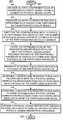
- FIG. 3illustrates a flow chart 300 of a method of partitioning an integrated circuit design for physical design verification according to an embodiment of the present invention.
- Step 302is the entry point of the flow chart 600 .
- step 304a representation of an integrated circuit design having a number of physical design layers is received as input via the user interface 202 in FIG. 2 .
- the representationis a GDS2 design database, however, other formats for representing a circuit design may also be used to practice the present invention within the scope of the appended claims.
- step 306a composite run deck such as the composite run deck 104 in FIG. 1 that specifies the rule checks to be performed on the integrated circuit design is received as input.
- the composite run deckis partitioned to create the partitioned run decks 202 so that the number of physical design layers referenced by each of the partitioned run decks 202 is a minimum as described above.
- the composite run deckmay be partitioned into eight partitioned run decks 202 based on functionality and layer dependencies associated with the rules in each of the partitioned run decks 202 .
- a sub-directoryis created for each of the eight partitioned run decks 202 for spawning off the physical verification process on each of the eight partitioned run decks 202 .
- the modular character of the partitioned run decksadvantageously enhances their maintainability, so that updates may readily be incorporated as needed.
- step 310the representation of the integrated circuit design is parsed to filter only the physical design layers required for each of the partitioned run decks to create a filtered data deck for each of the partitioned run decks.
- a metal-2 spacing rule checkrequires only the metal-2 design data from the GDS2 design file, so the portion of the filtered data deck created for the metal-2 spacing rule check would contain only the metal-2 design data from the GDS2 design file.
- Each of the filtered data decks 210 , 212 and 214is a reduced set of the GDS2 design database 108 that includes only the physical design layers required to perform the rule check for each corresponding partitioned run deck without undermining the thoroughness of the validation of the integrated circuit design with respect to each of the rules contained in the partitioned run decks.
- the filtering of the physical design layers to include only the physical design layers required to perform the rule check for the corresponding partitioned run deck 202is an important feature of the present invention.
- step 312the filtered data deck for each of the partitioned run decks is generated as output.
- a memory size required to run each filtered data deck on a physical design verification processoris determined from the filtered data deck for each of the partitioned run decks.
- Other resource characteristicssuch as processor speed and availability may also be weighed for intelligently distributing each filtered data deck to a physical design verification processor.
- each filtered data deckis assigned to a separate processor queue in a server farm according to the memory size and other resource considerations for each filtered data deck.
- the memory size required to run a filtered data deckis less than 3.5 gigabytes, and the physical design verification process for the filtered data deck may be assigned, for example, to a 32-bit LINUX server farm queue. If the size of the filtered data deck GDS2 file exceeds 3.5 gigabytes, then the physical design verification process for the filtered data deck may be assigned, for example, to a 64-bit SOLARIS server farm queue. The 3.5 gigabyte limit is unlikely to be exceeded, however, except for rule checks that require full database connectivity information.
- Each filtered data deckis accordingly assigned to a separate client processor that may be run concurrently with one other, advantageously reducing the turnaround time for the physical design verification of the entire integrated circuit design. Also, the assignment process may be fully automated to minimize user intervention during the physical design verification process.
- step 318a physical design verification is performed in parallel for each filtered data deck on each separate physical design verification processor.
- Step 320is the exit point of the flow chart 300 .
- the method of the present inventionprovides a flexible and robust architecture that can accommodate both in-house and third-party physical design verification tools and can work with a wide variety of computer resources.
- a computer program product for analyzing noise for an integrated circuit designincludes:
Landscapes
- Engineering & Computer Science (AREA)
- Computer Hardware Design (AREA)
- Physics & Mathematics (AREA)
- Theoretical Computer Science (AREA)
- Evolutionary Computation (AREA)
- Geometry (AREA)
- General Engineering & Computer Science (AREA)
- General Physics & Mathematics (AREA)
- Design And Manufacture Of Integrated Circuits (AREA)
Abstract
Description
- 1. Field of the Invention
- The present invention relates generally to the design of integrated circuits. More specifically, but without limitation thereto, the present invention relates to methods of partitioning an integrated circuit design into a smaller address space to increase efficiency of physical design verification tools.
- 2. Description of Related Art
- Physical design verification tools are typically run on 32-bit processors and 64-bit processors to verify integrated circuit designs represented by GDS2 files. The 32-bit processors have an address space that can accommodate integrated circuit designs up to 3.5 gigabytes in size, while the 64-bit processors have a larger address space that affords the capability of accommodating integrated designs larger than 3.5 gigabytes.
- In one aspect of the present invention, a method of partitioning an integrated circuit design for physical design verification includes steps of:
- (a) receiving as input a representation of an integrated circuit design having a number of physical design layers;
- (b) receiving as input a composite run deck specifying rule checks to be performed on the integrated circuit design;
- (c) partitioning the composite run deck into partitioned run decks so that the number of physical design layers referenced by each of the partitioned run decks is a minimum;
- (d) parsing the representation of the integrated circuit design to filter only the physical design layers required for each of the partitioned run decks into a filtered data deck for each of the partitioned run decks; and
- (e) generating as output the filtered data deck for each of the partitioned run decks.
- In another aspect of the present invention, a computer program product for partitioning an integrated circuit design for physical design verification includes:
- a medium for embodying a computer program for input to a computer; and
- a computer program embodied in the medium for causing the computer to perform steps of:
- (a) receiving as input a representation of an integrated circuit design having a number of physical design layers;
- (b) receiving as input a composite run deck specifying rule checks to be performed on the integrated circuit design;
- (c) partitioning the composite run deck into partitioned run decks so that the number of physical design layers referenced by each of the partitioned run decks is a minimum;
- (d) parsing the representation of the integrated circuit design to filter only the physical design layers required for each of the partitioned run decks into a filtered data deck for each of the partitioned run decks; and
- (e) generating as output the filtered data deck for each of the partitioned run decks.
- The present invention is illustrated by way of example and not limitation in the accompanying figures, in which like references indicate similar elements throughout the several views of the drawings, and in which:
FIG. 1 illustrates a flow diagram of a typical physical design verification process of the prior art;FIG. 2 illustrates a flow diagram of a physical design verification process according to an embodiment of the present invention; andFIG. 3 illustrates a flow chart of a method of partitioning an integrated circuit design for physical design verification according to an embodiment of the present invention.- Elements in the figures are illustrated for simplicity and clarity and have not necessarily been drawn to scale. For example, the dimensions of some elements in the figures may be exaggerated relative to other elements to point out distinctive features in the illustrated embodiments of the present invention.
- An important step in the design of integrated circuits is physical design verification, which ensures that all spatial constraints are satisfied for the traces and devices formed in various layers of an integrated circuit die. The structures formed in the several layers of an integrated circuit die are typically represented in a GDS2 (Graphic Data System stream format) file that contains the chip topological information for creating the masks used in manufacturing the integrated circuit dies. The GDS2 format is an industry standard used by commercially available physical verification tools to represent physical design data.
FIG. 1 illustrates a flow diagram of a typical physical design verification process of the prior art. Shown inFIG. 1 are auser interface 102, acomposite run deck 104, a stream-outtool 106, a GDS2design database 108, physical designverification side files 110, a physicaldesign verification environment 112, a PERL (Practical Extraction and Report Language)engine 114, a physicaldesign verification tool 116, physicaldesign verification results 118, and physical designverification log files 120.- The
user interface 102 includes a database of commercially available place and route tools that assist the circuit designer in optimizing placement and routing and to meet the timing constraints for a specific integrated design. - The
composite run deck 104 is a file that contains all the rules for verifying an integrated circuit design for a specific technology, for example, a transistor size of 0.18 micron, 0.13 micron or 0.09 micron, and/or layer-stack combination, that is, the number of metal layers used in the design. The metal layers may be used, for example, for connecting the functional blocks in the design, for routing clock nets, for distributing power, and for bonding out to the I/O pads of the chip. Thecomposite run deck 104 is typically a text file that implements the various rule requirements in a rule format such as the Standard Verification Rule Format (SVRF) commonly used by commercially available physical verification tools. - The stream-out
tool 106 generates a GDS2 file from the optimized design received from theuser interface 102. - The GDS2
design database 108 is the file generated by the stream-outtool 106 that contains the physical representation of the integrated circuit design optimized by theuser interface 102. The size of the GDS2 file varies according to the complexity of the integrated circuit design. - The physical design
verification side files 110 typically include information such as the name of the GDS2 file, the area or layout window of the physical design, a list of rule checks that are needed to verify the physical design, and other information for performing the verification of the physical design. - The physical
design verification environment 112 includes the PERL (Practical Extraction and Report Language)engine 114 and the physicaldesign verification tool 116. The PERLengine 114 parses and processes thecomposite run deck 104, the GDS2design database 108, and the physical designverification side files 110 to generate a wrapper file defining the locations of input and output files and the run deck for the physicaldesign verification tool 116. The physicaldesign verification tool 116 may be, for example, a commercially available software program that performs the verification of the physical design on the GDSdesign database 108 according to the wrapper file generated by the PERLengine 114 to validate the adherence of the integrated circuit design to the rules specified in thecomposite run deck 104. - The physical
design verification results 118 is a file that includes a summary of the rule checks performed on the integrated circuit design and the number of violations detected for each of the rules. - The physical design
verification log files 120 detail the locations within the GDSdesign database 108 of each of the rule violations so that the circuit designer can readily correct problems in an efficient manner. - Disadvantages of using the single
composite run deck 104 to verify all the design rules include the long run time required for large GDS2 design files, the inability to use economical processors such as 32-bit LINUX processors for integrated circuit designs larger than 3.5 gigabytes, and the lack of intelligent job-spawning capabilities to partition the rule checking among multiple processors. - It is generally advantageous to run physical design verification tools on processors having a memory bit width of, for example, 32 bits, which are generally faster and less expensive than larger 64-bit processors, however the 32-bit processors are limited to integrated circuit designs of no more than about 3.5 gigabytes in size. The method of the present invention overcomes the address space limitation of the 32-bit processors for integrated designs larger than 3.5 gigabytes by partitioning the integrated circuit design so that physical design verification may be performed by multiple 32-bit processors operating in parallel to reduce turnaround time and processor cost.
- In one aspect of the present invention, a method of partitioning an integrated circuit design for physical design verification includes steps of:
- (a) receiving as input a representation of an integrated circuit design having a number of physical design layers;
- (b) receiving as input a composite run deck specifying rule checks to be performed on the integrated circuit design;
- (c) partitioning the composite run deck into partitioned run decks so that the number of physical design layers referenced by each of the partitioned run decks is a minimum;
- (d) parsing the representation of the integrated circuit design to filter only the physical design layers required for each of the partitioned run decks into a filtered data deck for each of the partitioned run decks; and
- (e) generating as output the filtered data deck for each of the partitioned run decks.
FIG. 2 illustrates a flow diagram of a physical design verification process according to an embodiment of the present invention. Shown inFIG. 2 are auser interface 102, a stream-outtool 106, a GDS2design database 108, a PERL (Practical Extraction and Report Language)engine 114, partitionedrun decks 202, physicalverification tool processors data decks design verification tool 216.- The
user interface 102 generates inputs for the physicaldesign verification tool 216 for making appropriate decisions for setting up the validation flow, for example, information about the available server farm queues for assigning partitioned run decks as explained in further detail below. - The stream-out
tool 106, the GDS2design database 108, and PERL (Practical Extraction and Report Language)engine 114 may be the same as that described above forFIG. 1 . - The
partitioned run decks 202 are a partitioning of thecomposite run deck 104 ofFIG.1 . The partitioning is performed by identifying the physical design data that is referenced by each rule check. For example, some of the partitionedrun decks 202 are specific to metal layer rules, while others are specific to base layer rules, others to antenna rules, and so on. When the physical design data from theGDS2 design database 108 referenced by each rule check is identified, thecomposite run deck 104 is partitioned so that so that the number of physical design layers referenced by each of the partitionedrun decks 202 is a minimum, thereby ensuring that as many as possible of the partitionedrun decks 202 can be run on faster processors having less memory than larger, slower processors. Thepartitioned run decks 202 allows the GDS file108 to be parsed into the separate parseddata decks verification tool processors - The physical
design verification tool 216 filters theGDS design file 108 into the parseddata decks run decks 202 so that each of the parseddata decks GDS2 design database 108 that is required to perform the physical design verification for each corresponding partitionedrun deck 202. The physicaldesign verification tool 216 also assigns each of the parseddata decks verification tool processors design verification tool 216 uses information received from theuser interface 102 to determine the amount of memory available in the physicalverification tool processors - The physical
verification tool processors data decks GDS design database 108. and reducing the processor memory requirement so that use of processors having a memory bit width of, for example, 32 bits is maximized. This feature minimizes the resource requirements from slower, larger processors having a bit width of, for example, 64 bits. FIG. 3 illustrates aflow chart 300 of a method of partitioning an integrated circuit design for physical design verification according to an embodiment of the present invention.- Step302 is the entry point of the flow chart600.
- In
step 304, a representation of an integrated circuit design having a number of physical design layers is received as input via theuser interface 202 inFIG. 2 . In this example, the representation is a GDS2 design database, however, other formats for representing a circuit design may also be used to practice the present invention within the scope of the appended claims. - In
step 306, a composite run deck such as thecomposite run deck 104 inFIG. 1 that specifies the rule checks to be performed on the integrated circuit design is received as input. - In
step 308, the composite run deck is partitioned to create thepartitioned run decks 202 so that the number of physical design layers referenced by each of the partitionedrun decks 202 is a minimum as described above. For example, the composite run deck may be partitioned into eightpartitioned run decks 202 based on functionality and layer dependencies associated with the rules in each of the partitionedrun decks 202. A sub-directory is created for each of the eightpartitioned run decks 202 for spawning off the physical verification process on each of the eightpartitioned run decks 202. - The modular character of the partitioned run decks advantageously enhances their maintainability, so that updates may readily be incorporated as needed.
- In
step 310, the representation of the integrated circuit design is parsed to filter only the physical design layers required for each of the partitioned run decks to create a filtered data deck for each of the partitioned run decks. For example, a metal-2 spacing rule check requires only the metal-2 design data from the GDS2 design file, so the portion of the filtered data deck created for the metal-2 spacing rule check would contain only the metal-2 design data from the GDS2 design file. - In this example, three filtered
data decks data decks GDS2 design database 108 that includes only the physical design layers required to perform the rule check for each corresponding partitioned run deck without undermining the thoroughness of the validation of the integrated circuit design with respect to each of the rules contained in the partitioned run decks. The filtering of the physical design layers to include only the physical design layers required to perform the rule check for the corresponding partitionedrun deck 202 is an important feature of the present invention. - In
step 312, the filtered data deck for each of the partitioned run decks is generated as output. - In
step 314, a memory size required to run each filtered data deck on a physical design verification processor is determined from the filtered data deck for each of the partitioned run decks. Other resource characteristics such as processor speed and availability may also be weighed for intelligently distributing each filtered data deck to a physical design verification processor. - In
step 316, each filtered data deck is assigned to a separate processor queue in a server farm according to the memory size and other resource considerations for each filtered data deck. Typically, the memory size required to run a filtered data deck is less than 3.5 gigabytes, and the physical design verification process for the filtered data deck may be assigned, for example, to a 32-bit LINUX server farm queue. If the size of the filtered data deck GDS2 file exceeds 3.5 gigabytes, then the physical design verification process for the filtered data deck may be assigned, for example, to a 64-bit SOLARIS server farm queue. The 3.5 gigabyte limit is unlikely to be exceeded, however, except for rule checks that require full database connectivity information. Each filtered data deck is accordingly assigned to a separate client processor that may be run concurrently with one other, advantageously reducing the turnaround time for the physical design verification of the entire integrated circuit design. Also, the assignment process may be fully automated to minimize user intervention during the physical design verification process. - In
step 318, a physical design verification is performed in parallel for each filtered data deck on each separate physical design verification processor. - Step320 is the exit point of the
flow chart 300. - As may be appreciated from the above, the method of the present invention provides a flexible and robust architecture that can accommodate both in-house and third-party physical design verification tools and can work with a wide variety of computer resources.
- Although the method of the present invention illustrated by the flowchart descriptions above are described and shown with reference to specific steps performed in a specific order, these steps may be combined, sub-divided, or reordered without departing from the scope of the claims. Unless specifically indicated herein, the order and grouping of steps is not a limitation of the present invention.
- The steps described above with regard to the flow charts described above may also be implemented by instructions performed on a computer according to well-known computer programming techniques.
- In another aspect of the present invention, a computer program product for analyzing noise for an integrated circuit design includes:
- a medium for embodying a computer program for input to a computer; and
- a computer program embodied in the medium for causing the computer to perform steps of:
- (a) receiving as input a representation of an integrated circuit design having a number of physical design layers;
- (b) receiving as input a composite run deck specifying rule checks to be performed on the integrated circuit design;
- (c) partitioning the composite run deck into partitioned run decks so that the number of physical design layers referenced by each of the partitioned run decks is a minimum;
- (d) parsing the representation of the integrated circuit design to filter only the physical design layers required for each of the partitioned run decks into a filtered data deck for each of the partitioned run decks; and
- (e) generating as output the filtered data deck for each of the partitioned run decks.
- While the invention herein disclosed has been described by means of specific embodiments and applications thereof, numerous modifications and variations could be made thereto by those skilled in the art without departing from the scope of the invention set forth in the following claims.
Claims (14)
Priority Applications (1)
| Application Number | Priority Date | Filing Date | Title |
|---|---|---|---|
| US10/697,357US7107559B2 (en) | 2003-10-29 | 2003-10-29 | Method of partitioning an integrated circuit design for physical design verification |
Applications Claiming Priority (1)
| Application Number | Priority Date | Filing Date | Title |
|---|---|---|---|
| US10/697,357US7107559B2 (en) | 2003-10-29 | 2003-10-29 | Method of partitioning an integrated circuit design for physical design verification |
Publications (2)
| Publication Number | Publication Date |
|---|---|
| US20050097488A1true US20050097488A1 (en) | 2005-05-05 |
| US7107559B2 US7107559B2 (en) | 2006-09-12 |
Family
ID=34550337
Family Applications (1)
| Application Number | Title | Priority Date | Filing Date |
|---|---|---|---|
| US10/697,357Expired - LifetimeUS7107559B2 (en) | 2003-10-29 | 2003-10-29 | Method of partitioning an integrated circuit design for physical design verification |
Country Status (1)
| Country | Link |
|---|---|
| US (1) | US7107559B2 (en) |
Cited By (10)
| Publication number | Priority date | Publication date | Assignee | Title |
|---|---|---|---|---|
| US20060064656A1 (en)* | 2004-09-22 | 2006-03-23 | Viswanathan Lakshmanan | Method of early physical design validation and identification of texted metal short circuits in an integrated circuit design |
| US7155693B1 (en) | 2003-04-23 | 2006-12-26 | Magma Design Automation, Inc. | Floorplanning a hierarchical physical design to improve placement and routing |
| US7185305B1 (en) | 2000-11-15 | 2007-02-27 | Magma Design Automation, Inc. | Creating a power distribution arrangement with tapered metal wires for a physical design |
| US20070157140A1 (en)* | 2005-12-29 | 2007-07-05 | Holesovsky Alan L | Method and computer program product for trimming the analysis of physical layout versus schematic design comparison |
| US7353488B1 (en) | 2004-05-27 | 2008-04-01 | Magma Design Automation, Inc. | Flow definition language for designing integrated circuit implementation flows |
| US20080109778A1 (en)* | 2006-10-23 | 2008-05-08 | Inventec Corporation | Setting method of line pitch/line width layout for logic circuit |
| US20090049416A1 (en)* | 2005-12-12 | 2009-02-19 | International Business Machines Corporation | Computer Program Product for Extending Incremental Verification of Circuit Design to Encompass Verification Restraints |
| US8769468B1 (en)* | 2013-01-09 | 2014-07-01 | International Business Machines Corporation | Automatic generation of wire tag lists for a metal stack |
| US11461223B2 (en) | 2020-06-09 | 2022-10-04 | Methodics, Inc. | Efficient computing hardware and software component design testing through test fragmentation and isolated execution within a discrete computing environment |
| US11669439B2 (en)* | 2020-06-09 | 2023-06-06 | Methodics, Inc. | Computing hardware and software design testing auditability, including for critical control systems, functional safety, and autonomous vehicle component certification |
Families Citing this family (8)
| Publication number | Priority date | Publication date | Assignee | Title |
|---|---|---|---|---|
| US7913206B1 (en) | 2004-09-16 | 2011-03-22 | Cadence Design Systems, Inc. | Method and mechanism for performing partitioning of DRC operations |
| US7302654B2 (en)* | 2004-10-27 | 2007-11-27 | Lsi Corporation | Method of automating place and route corrections for an integrated circuit design from physical design validation |
| US7617464B2 (en)* | 2005-05-20 | 2009-11-10 | Synopsys, Inc. | Verifying an IC layout in individual regions and combining results |
| US7409656B1 (en) | 2005-09-12 | 2008-08-05 | Cadence Design Systems, Inc. | Method and system for parallelizing computing operations |
| US7904852B1 (en) | 2005-09-12 | 2011-03-08 | Cadence Design Systems, Inc. | Method and system for implementing parallel processing of electronic design automation tools |
| US8448096B1 (en) | 2006-06-30 | 2013-05-21 | Cadence Design Systems, Inc. | Method and system for parallel processing of IC design layouts |
| US7657856B1 (en) | 2006-09-12 | 2010-02-02 | Cadence Design Systems, Inc. | Method and system for parallel processing of IC design layouts |
| CN102054081A (en) | 2009-10-30 | 2011-05-11 | 新思科技有限公司 | Method and device for verifying physical design applied to integrated circuit |
Citations (14)
| Publication number | Priority date | Publication date | Assignee | Title |
|---|---|---|---|---|
| US5519628A (en)* | 1993-02-19 | 1996-05-21 | International Business Machines Corporation | System and method for formulating subsets of a hierarchical circuit design |
| US5528508A (en)* | 1993-02-19 | 1996-06-18 | International Business Machines Corporation | System and method for verifying a hierarchical circuit design |
| US5768585A (en)* | 1995-11-21 | 1998-06-16 | Intel Corporation | System and method for synchronizing multiple processors during power-on self testing |
| US6009251A (en)* | 1997-09-30 | 1999-12-28 | Synopsys, Inc. | Method and system for layout verification of an integrated circuit design with reusable subdesigns |
| US6289488B1 (en)* | 1997-02-24 | 2001-09-11 | Lucent Technologies Inc. | Hardware-software co-synthesis of hierarchical heterogeneous distributed embedded systems |
| US6378110B1 (en)* | 1998-03-31 | 2002-04-23 | Synopsys, Inc. | Layer-based rule checking for an integrated circuit layout |
| US20020138813A1 (en)* | 2001-03-20 | 2002-09-26 | Cheehoe Teh | System & method for performing design rule check |
| US6606735B1 (en)* | 1999-10-14 | 2003-08-12 | Synopsys, Inc. | Method and system for using error and filter layers in each DRC rule |
| US6668359B1 (en)* | 2001-10-31 | 2003-12-23 | Lsi Logic Corporation | Verilog to vital translator |
| US20040025126A1 (en)* | 2002-08-05 | 2004-02-05 | Culler Jason Harold | System and method for providing compliant mapping between chip bond locations and package bond locations for an integrated circuit |
| US6829754B1 (en)* | 2002-06-04 | 2004-12-07 | Lsi Logic Corporation | Method and system for checking for power errors in ASIC designs |
| US20050055654A1 (en)* | 2003-09-08 | 2005-03-10 | Jai-Ming Lin | Method for checking an IC layout |
| US20050108666A1 (en)* | 2003-11-06 | 2005-05-19 | Li-Fu Chang | Delta information design closure in integrated circuit fabrication |
| US20050125754A1 (en)* | 1999-11-30 | 2005-06-09 | Schubert Nils E. | Hardware debugging in a hardware description language |
- 2003
- 2003-10-29USUS10/697,357patent/US7107559B2/ennot_activeExpired - Lifetime
Patent Citations (15)
| Publication number | Priority date | Publication date | Assignee | Title |
|---|---|---|---|---|
| US5528508A (en)* | 1993-02-19 | 1996-06-18 | International Business Machines Corporation | System and method for verifying a hierarchical circuit design |
| US5519628A (en)* | 1993-02-19 | 1996-05-21 | International Business Machines Corporation | System and method for formulating subsets of a hierarchical circuit design |
| US5768585A (en)* | 1995-11-21 | 1998-06-16 | Intel Corporation | System and method for synchronizing multiple processors during power-on self testing |
| US6289488B1 (en)* | 1997-02-24 | 2001-09-11 | Lucent Technologies Inc. | Hardware-software co-synthesis of hierarchical heterogeneous distributed embedded systems |
| US6009251A (en)* | 1997-09-30 | 1999-12-28 | Synopsys, Inc. | Method and system for layout verification of an integrated circuit design with reusable subdesigns |
| US6378110B1 (en)* | 1998-03-31 | 2002-04-23 | Synopsys, Inc. | Layer-based rule checking for an integrated circuit layout |
| US6606735B1 (en)* | 1999-10-14 | 2003-08-12 | Synopsys, Inc. | Method and system for using error and filter layers in each DRC rule |
| US20050125754A1 (en)* | 1999-11-30 | 2005-06-09 | Schubert Nils E. | Hardware debugging in a hardware description language |
| US20020138813A1 (en)* | 2001-03-20 | 2002-09-26 | Cheehoe Teh | System & method for performing design rule check |
| US6816997B2 (en)* | 2001-03-20 | 2004-11-09 | Cheehoe Teh | System and method for performing design rule check |
| US6668359B1 (en)* | 2001-10-31 | 2003-12-23 | Lsi Logic Corporation | Verilog to vital translator |
| US6829754B1 (en)* | 2002-06-04 | 2004-12-07 | Lsi Logic Corporation | Method and system for checking for power errors in ASIC designs |
| US20040025126A1 (en)* | 2002-08-05 | 2004-02-05 | Culler Jason Harold | System and method for providing compliant mapping between chip bond locations and package bond locations for an integrated circuit |
| US20050055654A1 (en)* | 2003-09-08 | 2005-03-10 | Jai-Ming Lin | Method for checking an IC layout |
| US20050108666A1 (en)* | 2003-11-06 | 2005-05-19 | Li-Fu Chang | Delta information design closure in integrated circuit fabrication |
Cited By (17)
| Publication number | Priority date | Publication date | Assignee | Title |
|---|---|---|---|---|
| US7185305B1 (en) | 2000-11-15 | 2007-02-27 | Magma Design Automation, Inc. | Creating a power distribution arrangement with tapered metal wires for a physical design |
| US7155693B1 (en) | 2003-04-23 | 2006-12-26 | Magma Design Automation, Inc. | Floorplanning a hierarchical physical design to improve placement and routing |
| US20070136709A1 (en)* | 2003-04-23 | 2007-06-14 | Magma Design Automation, Inc. | Floorplanning A Hierarchical Physical Design To Improve Placement And Routing |
| US7353488B1 (en) | 2004-05-27 | 2008-04-01 | Magma Design Automation, Inc. | Flow definition language for designing integrated circuit implementation flows |
| US20060064656A1 (en)* | 2004-09-22 | 2006-03-23 | Viswanathan Lakshmanan | Method of early physical design validation and identification of texted metal short circuits in an integrated circuit design |
| US7149989B2 (en)* | 2004-09-22 | 2006-12-12 | Lsi Logic Corporation | Method of early physical design validation and identification of texted metal short circuits in an integrated circuit design |
| US7779378B2 (en) | 2005-12-12 | 2010-08-17 | International Business Machines Corporation | Computer program product for extending incremental verification of circuit design to encompass verification restraints |
| US20090049416A1 (en)* | 2005-12-12 | 2009-02-19 | International Business Machines Corporation | Computer Program Product for Extending Incremental Verification of Circuit Design to Encompass Verification Restraints |
| US7480878B2 (en)* | 2005-12-29 | 2009-01-20 | Lsi Logic Corportion | Method and system for layout versus schematic validation of integrated circuit designs |
| US20070157140A1 (en)* | 2005-12-29 | 2007-07-05 | Holesovsky Alan L | Method and computer program product for trimming the analysis of physical layout versus schematic design comparison |
| US20080109778A1 (en)* | 2006-10-23 | 2008-05-08 | Inventec Corporation | Setting method of line pitch/line width layout for logic circuit |
| US8769468B1 (en)* | 2013-01-09 | 2014-07-01 | International Business Machines Corporation | Automatic generation of wire tag lists for a metal stack |
| CN103914585A (en)* | 2013-01-09 | 2014-07-09 | 国际商业机器公司 | Automatic generation of wire tag lists for a metal stack |
| US20140223397A1 (en)* | 2013-01-09 | 2014-08-07 | International Business Machines Corporation | Automatic Generation of Wire Tag Lists for a Metal Stack |
| US9092591B2 (en)* | 2013-01-09 | 2015-07-28 | International Business Machines Corporation | Automatic generation of wire tag lists for a metal stack |
| US11461223B2 (en) | 2020-06-09 | 2022-10-04 | Methodics, Inc. | Efficient computing hardware and software component design testing through test fragmentation and isolated execution within a discrete computing environment |
| US11669439B2 (en)* | 2020-06-09 | 2023-06-06 | Methodics, Inc. | Computing hardware and software design testing auditability, including for critical control systems, functional safety, and autonomous vehicle component certification |
Also Published As
| Publication number | Publication date |
|---|---|
| US7107559B2 (en) | 2006-09-12 |
Similar Documents
| Publication | Publication Date | Title |
|---|---|---|
| US7107559B2 (en) | Method of partitioning an integrated circuit design for physical design verification | |
| US7107568B2 (en) | System and method for reducing wire delay or congestion during synthesis of hardware solvers | |
| US8423605B2 (en) | Parallel distributed processing method and computer system | |
| US6990651B2 (en) | Advanced design format library for integrated circuit design synthesis and floorplanning tools | |
| US5553001A (en) | Method for optimizing resource allocation starting from a high level | |
| US20190079794A1 (en) | Flexible physical function and virtual function mapping | |
| WO2009079244A1 (en) | System and method for routing connections | |
| US7376921B2 (en) | Methods for tiling integrated circuit designs | |
| US9256707B2 (en) | Trace routing according to freeform sketches | |
| US8127259B2 (en) | Synthesis constraint creating device, behavioral synthesis device, synthesis constraint creating method and recording medium | |
| US7302654B2 (en) | Method of automating place and route corrections for an integrated circuit design from physical design validation | |
| US8006215B1 (en) | Circuit clustering during placement | |
| US20080301607A1 (en) | Method, system, and computer program product for hierarchical integrated circuit repartitioning | |
| US7260803B2 (en) | Incremental dummy metal insertions | |
| US8631375B2 (en) | Via selection in integrated circuit design | |
| US7222321B2 (en) | System and method for manipulating an integrated circuit layout | |
| US8055733B2 (en) | Method, apparatus, and computer program product for implementing importation and converging system definitions during planning phase for logical partition (LPAR) systems | |
| Chang et al. | ECO optimization using metal-configurable gate-array spare cells | |
| JP3193167B2 (en) | Logic synthesis system | |
| US20030177456A1 (en) | Method, system and computer product to translate electronic schematic files between computer aided design platforms | |
| US20050138580A1 (en) | Method of generating dependency specification file capable of reconfiguring function block of soft IP and recording medium storing codes embodying the method | |
| CN118210457B (en) | Metamodel-based SaaS metadata layered migration method and device | |
| US20040025131A1 (en) | Method and apparatus for placing repeater banks in integrated circuit design | |
| CN120179408A (en) | Server partitioning method, server and storage medium | |
| JP2715931B2 (en) | Semiconductor integrated circuit design support method |
Legal Events
| Date | Code | Title | Description |
|---|---|---|---|
| AS | Assignment | Owner name:LSI LOGIC CORPORATION, CALIFORNIA Free format text:ASSIGNMENT OF ASSIGNORS INTEREST;ASSIGNORS:LAKSHMANAN, VISWANATHAN;BLINNE, RICHARD D.;KUPPINGER, JONATHAN P.;REEL/FRAME:014660/0720 Effective date:20031024 | |
| STCF | Information on status: patent grant | Free format text:PATENTED CASE | |
| FEPP | Fee payment procedure | Free format text:PAYOR NUMBER ASSIGNED (ORIGINAL EVENT CODE: ASPN); ENTITY STATUS OF PATENT OWNER: LARGE ENTITY | |
| FPAY | Fee payment | Year of fee payment:4 | |
| FPAY | Fee payment | Year of fee payment:8 | |
| AS | Assignment | Owner name:DEUTSCHE BANK AG NEW YORK BRANCH, AS COLLATERAL AG Free format text:PATENT SECURITY AGREEMENT;ASSIGNORS:LSI CORPORATION;AGERE SYSTEMS LLC;REEL/FRAME:032856/0031 Effective date:20140506 | |
| AS | Assignment | Owner name:LSI CORPORATION, CALIFORNIA Free format text:CHANGE OF NAME;ASSIGNOR:LSI LOGIC CORPORATION;REEL/FRAME:033102/0270 Effective date:20070406 | |
| AS | Assignment | Owner name:AVAGO TECHNOLOGIES GENERAL IP (SINGAPORE) PTE. LTD Free format text:ASSIGNMENT OF ASSIGNORS INTEREST;ASSIGNOR:LSI CORPORATION;REEL/FRAME:035390/0388 Effective date:20140814 | |
| AS | Assignment | Owner name:AGERE SYSTEMS LLC, PENNSYLVANIA Free format text:TERMINATION AND RELEASE OF SECURITY INTEREST IN PATENT RIGHTS (RELEASES RF 032856-0031);ASSIGNOR:DEUTSCHE BANK AG NEW YORK BRANCH, AS COLLATERAL AGENT;REEL/FRAME:037684/0039 Effective date:20160201 Owner name:LSI CORPORATION, CALIFORNIA Free format text:TERMINATION AND RELEASE OF SECURITY INTEREST IN PATENT RIGHTS (RELEASES RF 032856-0031);ASSIGNOR:DEUTSCHE BANK AG NEW YORK BRANCH, AS COLLATERAL AGENT;REEL/FRAME:037684/0039 Effective date:20160201 | |
| AS | Assignment | Owner name:BANK OF AMERICA, N.A., AS COLLATERAL AGENT, NORTH CAROLINA Free format text:PATENT SECURITY AGREEMENT;ASSIGNOR:AVAGO TECHNOLOGIES GENERAL IP (SINGAPORE) PTE. LTD.;REEL/FRAME:037808/0001 Effective date:20160201 Owner name:BANK OF AMERICA, N.A., AS COLLATERAL AGENT, NORTH Free format text:PATENT SECURITY AGREEMENT;ASSIGNOR:AVAGO TECHNOLOGIES GENERAL IP (SINGAPORE) PTE. LTD.;REEL/FRAME:037808/0001 Effective date:20160201 | |
| AS | Assignment | Owner name:AVAGO TECHNOLOGIES GENERAL IP (SINGAPORE) PTE. LTD., SINGAPORE Free format text:TERMINATION AND RELEASE OF SECURITY INTEREST IN PATENTS;ASSIGNOR:BANK OF AMERICA, N.A., AS COLLATERAL AGENT;REEL/FRAME:041710/0001 Effective date:20170119 Owner name:AVAGO TECHNOLOGIES GENERAL IP (SINGAPORE) PTE. LTD Free format text:TERMINATION AND RELEASE OF SECURITY INTEREST IN PATENTS;ASSIGNOR:BANK OF AMERICA, N.A., AS COLLATERAL AGENT;REEL/FRAME:041710/0001 Effective date:20170119 | |
| AS | Assignment | Owner name:BELL SEMICONDUCTOR, LLC, ILLINOIS Free format text:ASSIGNMENT OF ASSIGNORS INTEREST;ASSIGNORS:AVAGO TECHNOLOGIES GENERAL IP (SINGAPORE) PTE. LTD.;BROADCOM CORPORATION;REEL/FRAME:044887/0109 Effective date:20171208 | |
| AS | Assignment | Owner name:CORTLAND CAPITAL MARKET SERVICES LLC, AS COLLATERA Free format text:SECURITY INTEREST;ASSIGNORS:HILCO PATENT ACQUISITION 56, LLC;BELL SEMICONDUCTOR, LLC;BELL NORTHERN RESEARCH, LLC;REEL/FRAME:045216/0020 Effective date:20180124 | |
| MAFP | Maintenance fee payment | Free format text:PAYMENT OF MAINTENANCE FEE, 12TH YEAR, LARGE ENTITY (ORIGINAL EVENT CODE: M1553) Year of fee payment:12 | |
| AS | Assignment | Owner name:BELL NORTHERN RESEARCH, LLC, ILLINOIS Free format text:RELEASE BY SECURED PARTY;ASSIGNOR:CORTLAND CAPITAL MARKET SERVICES LLC;REEL/FRAME:059720/0223 Effective date:20220401 Owner name:BELL SEMICONDUCTOR, LLC, ILLINOIS Free format text:RELEASE BY SECURED PARTY;ASSIGNOR:CORTLAND CAPITAL MARKET SERVICES LLC;REEL/FRAME:059720/0223 Effective date:20220401 Owner name:HILCO PATENT ACQUISITION 56, LLC, ILLINOIS Free format text:RELEASE BY SECURED PARTY;ASSIGNOR:CORTLAND CAPITAL MARKET SERVICES LLC;REEL/FRAME:059720/0223 Effective date:20220401 |