US20050095422A1 - Inorganic/organic hybrid nanolaminate barrier film - Google Patents
Inorganic/organic hybrid nanolaminate barrier filmDownload PDFInfo
- Publication number
- US20050095422A1 US20050095422A1US10/698,988US69898803AUS2005095422A1US 20050095422 A1US20050095422 A1US 20050095422A1US 69898803 AUS69898803 AUS 69898803AUS 2005095422 A1US2005095422 A1US 2005095422A1
- Authority
- US
- United States
- Prior art keywords
- barrier film
- day
- layers
- fluorinated
- organic
- Prior art date
- Legal status (The legal status is an assumption and is not a legal conclusion. Google has not performed a legal analysis and makes no representation as to the accuracy of the status listed.)
- Granted
Links
- 230000004888barrier functionEffects0.000titleclaimsabstractdescription55
- 238000000034methodMethods0.000claimsabstractdescription18
- 239000011368organic materialSubstances0.000claimsabstractdescription8
- 229910010272inorganic materialInorganic materials0.000claimsabstractdescription7
- 239000011147inorganic materialSubstances0.000claimsabstractdescription7
- 239000010410layerSubstances0.000claimsdescription47
- 239000002243precursorSubstances0.000claimsdescription29
- LFQSCWFLJHTTHZ-UHFFFAOYSA-NEthanolChemical compoundCCOLFQSCWFLJHTTHZ-UHFFFAOYSA-N0.000claimsdescription27
- 229920000642polymerPolymers0.000claimsdescription26
- 238000000576coating methodMethods0.000claimsdescription24
- XLYOFNOQVPJJNP-UHFFFAOYSA-NwaterSubstancesOXLYOFNOQVPJJNP-UHFFFAOYSA-N0.000claimsdescription19
- 239000004094surface-active agentSubstances0.000claimsdescription18
- 239000000203mixtureSubstances0.000claimsdescription16
- 239000011248coating agentSubstances0.000claimsdescription14
- 239000000758substrateSubstances0.000claimsdescription12
- QVGXLLKOCUKJST-UHFFFAOYSA-Natomic oxygenChemical compound[O]QVGXLLKOCUKJST-UHFFFAOYSA-N0.000claimsdescription11
- 125000001165hydrophobic groupChemical group0.000claimsdescription11
- 239000012044organic layerSubstances0.000claimsdescription11
- 229910052760oxygenInorganic materials0.000claimsdescription11
- 239000001301oxygenSubstances0.000claimsdescription11
- 230000035699permeabilityEffects0.000claimsdescription11
- BOTDANWDWHJENH-UHFFFAOYSA-NTetraethyl orthosilicateChemical compoundCCO[Si](OCC)(OCC)OCCBOTDANWDWHJENH-UHFFFAOYSA-N0.000claimsdescription8
- 150000004703alkoxidesChemical class0.000claimsdescription7
- 239000000178monomerSubstances0.000claimsdescription7
- -1Ba2+ cationsChemical class0.000claimsdescription6
- 239000004696Poly ether ether ketoneSubstances0.000claimsdescription6
- 239000000693micelleSubstances0.000claimsdescription6
- 230000005693optoelectronicsEffects0.000claimsdescription6
- 229920002530polyetherether ketonePolymers0.000claimsdescription6
- 239000003795chemical substances by applicationSubstances0.000claimsdescription5
- 229920000058polyacrylatePolymers0.000claimsdescription5
- 239000011112polyethylene naphthalateSubstances0.000claimsdescription5
- YGYNBBAUIYTWBF-UHFFFAOYSA-N2,6-dimethylnaphthaleneChemical compoundC1=C(C)C=CC2=CC(C)=CC=C21YGYNBBAUIYTWBF-UHFFFAOYSA-N0.000claimsdescription4
- LZZYPRNAOMGNLH-UHFFFAOYSA-MCetrimonium bromideChemical group[Br-].CCCCCCCCCCCCCCCC[N+](C)(C)CLZZYPRNAOMGNLH-UHFFFAOYSA-M0.000claimsdescription4
- IISBACLAFKSPIT-UHFFFAOYSA-Nbisphenol AChemical compoundC=1C=C(O)C=CC=1C(C)(C)C1=CC=C(O)C=C1IISBACLAFKSPIT-UHFFFAOYSA-N0.000claimsdescription4
- 239000007822coupling agentSubstances0.000claimsdescription4
- 238000000151depositionMethods0.000claimsdescription4
- 230000003075superhydrophobic effectEffects0.000claimsdescription4
- XDLMVUHYZWKMMD-UHFFFAOYSA-N3-trimethoxysilylpropyl 2-methylprop-2-enoateChemical compoundCO[Si](OC)(OC)CCCOC(=O)C(C)=CXDLMVUHYZWKMMD-UHFFFAOYSA-N0.000claimsdescription3
- 239000004971Cross linkerSubstances0.000claimsdescription3
- QNAYBMKLOCPYGJ-REOHCLBHSA-NL-alanineChemical compoundC[C@H](N)C(O)=OQNAYBMKLOCPYGJ-REOHCLBHSA-N0.000claimsdescription3
- AGPKZVBTJJNPAG-WHFBIAKZSA-NL-isoleucineChemical compoundCC[C@H](C)[C@H](N)C(O)=OAGPKZVBTJJNPAG-WHFBIAKZSA-N0.000claimsdescription3
- ROHFNLRQFUQHCH-YFKPBYRVSA-NL-leucineChemical compoundCC(C)C[C@H](N)C(O)=OROHFNLRQFUQHCH-YFKPBYRVSA-N0.000claimsdescription3
- FFEARJCKVFRZRR-BYPYZUCNSA-NL-methionineChemical compoundCSCC[C@H](N)C(O)=OFFEARJCKVFRZRR-BYPYZUCNSA-N0.000claimsdescription3
- COLNVLDHVKWLRT-QMMMGPOBSA-NL-phenylalanineChemical compoundOC(=O)[C@@H](N)CC1=CC=CC=C1COLNVLDHVKWLRT-QMMMGPOBSA-N0.000claimsdescription3
- QIVBCDIJIAJPQS-VIFPVBQESA-NL-tryptophaneChemical compoundC1=CC=C2C(C[C@H](N)C(O)=O)=CNC2=C1QIVBCDIJIAJPQS-VIFPVBQESA-N0.000claimsdescription3
- OUYCCCASQSFEME-QMMMGPOBSA-NL-tyrosineChemical compoundOC(=O)[C@@H](N)CC1=CC=C(O)C=C1OUYCCCASQSFEME-QMMMGPOBSA-N0.000claimsdescription3
- KZSNJWFQEVHDMF-BYPYZUCNSA-NL-valineChemical compoundCC(C)[C@H](N)C(O)=OKZSNJWFQEVHDMF-BYPYZUCNSA-N0.000claimsdescription3
- ROHFNLRQFUQHCH-UHFFFAOYSA-NLeucineNatural productsCC(C)CC(N)C(O)=OROHFNLRQFUQHCH-UHFFFAOYSA-N0.000claimsdescription3
- 229920012266Poly(ether sulfone) PESPolymers0.000claimsdescription3
- QIVBCDIJIAJPQS-UHFFFAOYSA-NTryptophanNatural productsC1=CC=C2C(CC(N)C(O)=O)=CNC2=C1QIVBCDIJIAJPQS-UHFFFAOYSA-N0.000claimsdescription3
- KZSNJWFQEVHDMF-UHFFFAOYSA-NValineNatural productsCC(C)C(N)C(O)=OKZSNJWFQEVHDMF-UHFFFAOYSA-N0.000claimsdescription3
- 235000004279alanineNutrition0.000claimsdescription3
- 125000003118aryl groupChemical group0.000claimsdescription3
- 125000001797benzyl groupChemical group[H]C1=C([H])C([H])=C(C([H])=C1[H])C([H])([H])*0.000claimsdescription3
- 230000015572biosynthetic processEffects0.000claimsdescription3
- 229910001914chlorine tetroxideInorganic materials0.000claimsdescription3
- 238000003618dip coatingMethods0.000claimsdescription3
- 239000003999initiatorSubstances0.000claimsdescription3
- 229960000310isoleucineDrugs0.000claimsdescription3
- AGPKZVBTJJNPAG-UHFFFAOYSA-NisoleucineNatural productsCCC(C)C(N)C(O)=OAGPKZVBTJJNPAG-UHFFFAOYSA-N0.000claimsdescription3
- 238000004519manufacturing processMethods0.000claimsdescription3
- 229930182817methionineNatural products0.000claimsdescription3
- 125000002496methyl groupChemical group[H]C([H])([H])*0.000claimsdescription3
- VLTRZXGMWDSKGL-UHFFFAOYSA-MperchlorateChemical compound[O-]Cl(=O)(=O)=OVLTRZXGMWDSKGL-UHFFFAOYSA-M0.000claimsdescription3
- COLNVLDHVKWLRT-UHFFFAOYSA-NphenylalanineNatural productsOC(=O)C(N)CC1=CC=CC=C1COLNVLDHVKWLRT-UHFFFAOYSA-N0.000claimsdescription3
- 238000004528spin coatingMethods0.000claimsdescription3
- OUYCCCASQSFEME-UHFFFAOYSA-NtyrosineNatural productsOC(=O)C(N)CC1=CC=C(O)C=C1OUYCCCASQSFEME-UHFFFAOYSA-N0.000claimsdescription3
- 239000004474valineSubstances0.000claimsdescription3
- 239000004695Polyether sulfoneSubstances0.000claimsdescription2
- 238000000137annealingMethods0.000claimsdescription2
- 235000013361beverageNutrition0.000claimsdescription2
- 235000009508confectioneryNutrition0.000claimsdescription2
- 238000000354decomposition reactionMethods0.000claimsdescription2
- 235000013305foodNutrition0.000claimsdescription2
- 238000010438heat treatmentMethods0.000claimsdescription2
- 235000021485packed foodNutrition0.000claimsdescription2
- 239000000825pharmaceutical preparationSubstances0.000claimsdescription2
- 229940127557pharmaceutical productDrugs0.000claimsdescription2
- 229920003207poly(ethylene-2,6-naphthalate)Polymers0.000claimsdescription2
- 229920006393polyether sulfonePolymers0.000claimsdescription2
- 238000005507sprayingMethods0.000claimsdescription2
- QROGIFZRVHSFLM-UHFFFAOYSA-Nprop-1-enylbenzeneChemical classCC=CC1=CC=CC=C1QROGIFZRVHSFLM-UHFFFAOYSA-N0.000claims2
- 150000003440styrenesChemical class0.000claims2
- IXCSERBJSXMMFS-UHFFFAOYSA-Nhydrogen chlorideSubstancesCl.ClIXCSERBJSXMMFS-UHFFFAOYSA-N0.000claims1
- 238000001338self-assemblyMethods0.000abstractdescription6
- 239000002114nanocompositeSubstances0.000abstractdescription3
- 239000010408filmSubstances0.000description29
- 239000000463materialSubstances0.000description10
- VEXZGXHMUGYJMC-UHFFFAOYSA-NHydrochloric acidChemical compoundClVEXZGXHMUGYJMC-UHFFFAOYSA-N0.000description6
- PPBRXRYQALVLMV-UHFFFAOYSA-NStyreneChemical compoundC=CC1=CC=CC=C1PPBRXRYQALVLMV-UHFFFAOYSA-N0.000description4
- KPUWHANPEXNPJT-UHFFFAOYSA-NdisiloxaneChemical class[SiH3]O[SiH3]KPUWHANPEXNPJT-UHFFFAOYSA-N0.000description4
- 238000001704evaporationMethods0.000description4
- 230000008020evaporationEffects0.000description4
- 230000002209hydrophobic effectEffects0.000description4
- 239000004033plasticSubstances0.000description4
- 229920003023plasticPolymers0.000description4
- 239000010409thin filmSubstances0.000description4
- 150000001450anionsChemical class0.000description3
- 150000001768cationsChemical class0.000description3
- 230000007613environmental effectEffects0.000description3
- 230000003993interactionEffects0.000description3
- 238000006116polymerization reactionMethods0.000description3
- 239000010936titaniumSubstances0.000description3
- OGBWMWKMTUSNKE-UHFFFAOYSA-N1-(2-methylprop-2-enoyloxy)hexyl 2-methylprop-2-enoateChemical compoundCCCCCC(OC(=O)C(C)=C)OC(=O)C(C)=COGBWMWKMTUSNKE-UHFFFAOYSA-N0.000description2
- JLBJTVDPSNHSKJ-UHFFFAOYSA-N4-MethylstyreneChemical compoundCC1=CC=C(C=C)C=C1JLBJTVDPSNHSKJ-UHFFFAOYSA-N0.000description2
- LCGLNKUTAGEVQW-UHFFFAOYSA-NDimethyl etherChemical compoundCOCLCGLNKUTAGEVQW-UHFFFAOYSA-N0.000description2
- 229910052581Si3N4Inorganic materials0.000description2
- VYPSYNLAJGMNEJ-UHFFFAOYSA-NSilicium dioxideChemical compoundO=[Si]=OVYPSYNLAJGMNEJ-UHFFFAOYSA-N0.000description2
- KYIKRXIYLAGAKQ-UHFFFAOYSA-NabcnChemical compoundC1CCCCC1(C#N)N=NC1(C#N)CCCCC1KYIKRXIYLAGAKQ-UHFFFAOYSA-N0.000description2
- 238000013459approachMethods0.000description2
- ISAOCJYIOMOJEB-UHFFFAOYSA-NbenzoinChemical compoundC=1C=CC=CC=1C(O)C(=O)C1=CC=CC=C1ISAOCJYIOMOJEB-UHFFFAOYSA-N0.000description2
- 239000007789gasSubstances0.000description2
- 239000011521glassSubstances0.000description2
- 238000010348incorporationMethods0.000description2
- 230000000977initiatory effectEffects0.000description2
- 229910052751metalInorganic materials0.000description2
- 239000002184metalSubstances0.000description2
- 229910052719titaniumInorganic materials0.000description2
- VXUYXOFXAQZZMF-UHFFFAOYSA-Ntitanium(IV) isopropoxideChemical compoundCC(C)O[Ti](OC(C)C)(OC(C)C)OC(C)CVXUYXOFXAQZZMF-UHFFFAOYSA-N0.000description2
- NIXOWILDQLNWCW-UHFFFAOYSA-MAcrylateChemical compound[O-]C(=O)C=CNIXOWILDQLNWCW-UHFFFAOYSA-M0.000description1
- 102100020870La-related protein 6Human genes0.000description1
- 108050008265La-related protein 6Proteins0.000description1
- 239000004698PolyethyleneSubstances0.000description1
- XUIMIQQOPSSXEZ-UHFFFAOYSA-NSiliconChemical compound[Si]XUIMIQQOPSSXEZ-UHFFFAOYSA-N0.000description1
- 244000028419Styrax benzoinSpecies0.000description1
- 235000000126Styrax benzoinNutrition0.000description1
- 235000008411Sumatra benzointreeNutrition0.000description1
- RTAQQCXQSZGOHL-UHFFFAOYSA-NTitaniumChemical compound[Ti]RTAQQCXQSZGOHL-UHFFFAOYSA-N0.000description1
- 230000004075alterationEffects0.000description1
- 229910052782aluminiumInorganic materials0.000description1
- PNEYBMLMFCGWSK-UHFFFAOYSA-Naluminium oxideInorganic materials[O-2].[O-2].[O-2].[Al+3].[Al+3]PNEYBMLMFCGWSK-UHFFFAOYSA-N0.000description1
- 229940024606amino acidDrugs0.000description1
- 235000001014amino acidNutrition0.000description1
- 150000001413amino acidsChemical class0.000description1
- 229910052788bariumInorganic materials0.000description1
- 230000008901benefitEffects0.000description1
- 229960002130benzoinDrugs0.000description1
- 230000005540biological transmissionEffects0.000description1
- 229910052796boronInorganic materials0.000description1
- 229910052793cadmiumInorganic materials0.000description1
- 238000006243chemical reactionMethods0.000description1
- 229910052804chromiumInorganic materials0.000description1
- 238000004140cleaningMethods0.000description1
- 229910052681coesiteInorganic materials0.000description1
- 239000002131composite materialSubstances0.000description1
- 150000001875compoundsChemical class0.000description1
- 238000009833condensationMethods0.000description1
- 230000005494condensationEffects0.000description1
- 229910052802copperInorganic materials0.000description1
- 229910052593corundumInorganic materials0.000description1
- 229910052906cristobaliteInorganic materials0.000description1
- 230000008021depositionEffects0.000description1
- 238000010586diagramMethods0.000description1
- 239000006185dispersionSubstances0.000description1
- 239000000975dyeSubstances0.000description1
- 229910052737goldInorganic materials0.000description1
- 235000019382gum benzoicNutrition0.000description1
- DKAGJZJALZXOOV-UHFFFAOYSA-Nhydrate;hydrochlorideChemical compoundO.ClDKAGJZJALZXOOV-UHFFFAOYSA-N0.000description1
- 229910052741iridiumInorganic materials0.000description1
- 229910052742ironInorganic materials0.000description1
- 229910052745leadInorganic materials0.000description1
- 239000004973liquid crystal related substanceSubstances0.000description1
- 230000002535lyotropic effectEffects0.000description1
- 229910052748manganeseInorganic materials0.000description1
- 229910044991metal oxideInorganic materials0.000description1
- 150000004706metal oxidesChemical class0.000description1
- 238000012986modificationMethods0.000description1
- 230000004048modificationEffects0.000description1
- 229910052750molybdenumInorganic materials0.000description1
- 239000002086nanomaterialSubstances0.000description1
- 229910052758niobiumInorganic materials0.000description1
- 150000004767nitridesChemical class0.000description1
- 230000003287optical effectEffects0.000description1
- 239000000049pigmentSubstances0.000description1
- 229920000573polyethylenePolymers0.000description1
- 239000002861polymer materialSubstances0.000description1
- 229920000307polymer substratePolymers0.000description1
- 230000000379polymerizing effectEffects0.000description1
- 229920001296polysiloxanePolymers0.000description1
- 238000002360preparation methodMethods0.000description1
- 230000008569processEffects0.000description1
- 238000012545processingMethods0.000description1
- 150000004760silicatesChemical class0.000description1
- 229910052710siliconInorganic materials0.000description1
- 239000010703siliconSubstances0.000description1
- 239000000377silicon dioxideSubstances0.000description1
- HQVNEWCFYHHQES-UHFFFAOYSA-Nsilicon nitrideChemical compoundN12[Si]34N5[Si]62N3[Si]51N64HQVNEWCFYHHQES-UHFFFAOYSA-N0.000description1
- 229910052709silverInorganic materials0.000description1
- 239000002356single layerSubstances0.000description1
- 238000000638solvent extractionMethods0.000description1
- 238000004544sputter depositionMethods0.000description1
- 238000003756stirringMethods0.000description1
- 229910052682stishoviteInorganic materials0.000description1
- 239000000126substanceSubstances0.000description1
- 229910052715tantalumInorganic materials0.000description1
- 229910052718tinInorganic materials0.000description1
- JMXKSZRRTHPKDL-UHFFFAOYSA-Ntitanium ethoxideChemical compound[Ti+4].CC[O-].CC[O-].CC[O-].CC[O-]JMXKSZRRTHPKDL-UHFFFAOYSA-N0.000description1
- 229910052723transition metalInorganic materials0.000description1
- 150000003624transition metalsChemical class0.000description1
- 229910052905tridymiteInorganic materials0.000description1
- 229910052721tungstenInorganic materials0.000description1
- 229910052720vanadiumInorganic materials0.000description1
- 229910001845yogo sapphireInorganic materials0.000description1
- 229910052727yttriumInorganic materials0.000description1
- 229910052725zincInorganic materials0.000description1
- 229910052726zirconiumInorganic materials0.000description1
Images

Classifications
- B—PERFORMING OPERATIONS; TRANSPORTING
- B05—SPRAYING OR ATOMISING IN GENERAL; APPLYING FLUENT MATERIALS TO SURFACES, IN GENERAL
- B05D—PROCESSES FOR APPLYING FLUENT MATERIALS TO SURFACES, IN GENERAL
- B05D7/00—Processes, other than flocking, specially adapted for applying liquids or other fluent materials to particular surfaces or for applying particular liquids or other fluent materials
- B05D7/50—Multilayers
- B05D7/56—Three layers or more
- B—PERFORMING OPERATIONS; TRANSPORTING
- B05—SPRAYING OR ATOMISING IN GENERAL; APPLYING FLUENT MATERIALS TO SURFACES, IN GENERAL
- B05D—PROCESSES FOR APPLYING FLUENT MATERIALS TO SURFACES, IN GENERAL
- B05D1/00—Processes for applying liquids or other fluent materials
- B05D1/002—Processes for applying liquids or other fluent materials the substrate being rotated
- B05D1/005—Spin coating
- B—PERFORMING OPERATIONS; TRANSPORTING
- B05—SPRAYING OR ATOMISING IN GENERAL; APPLYING FLUENT MATERIALS TO SURFACES, IN GENERAL
- B05D—PROCESSES FOR APPLYING FLUENT MATERIALS TO SURFACES, IN GENERAL
- B05D1/00—Processes for applying liquids or other fluent materials
- B05D1/02—Processes for applying liquids or other fluent materials performed by spraying
- B—PERFORMING OPERATIONS; TRANSPORTING
- B05—SPRAYING OR ATOMISING IN GENERAL; APPLYING FLUENT MATERIALS TO SURFACES, IN GENERAL
- B05D—PROCESSES FOR APPLYING FLUENT MATERIALS TO SURFACES, IN GENERAL
- B05D1/00—Processes for applying liquids or other fluent materials
- B05D1/18—Processes for applying liquids or other fluent materials performed by dipping
- B—PERFORMING OPERATIONS; TRANSPORTING
- B05—SPRAYING OR ATOMISING IN GENERAL; APPLYING FLUENT MATERIALS TO SURFACES, IN GENERAL
- B05D—PROCESSES FOR APPLYING FLUENT MATERIALS TO SURFACES, IN GENERAL
- B05D1/00—Processes for applying liquids or other fluent materials
- B05D1/30—Processes for applying liquids or other fluent materials performed by gravity only, i.e. flow coating
- B—PERFORMING OPERATIONS; TRANSPORTING
- B05—SPRAYING OR ATOMISING IN GENERAL; APPLYING FLUENT MATERIALS TO SURFACES, IN GENERAL
- B05D—PROCESSES FOR APPLYING FLUENT MATERIALS TO SURFACES, IN GENERAL
- B05D3/00—Pretreatment of surfaces to which liquids or other fluent materials are to be applied; After-treatment of applied coatings, e.g. intermediate treating of an applied coating preparatory to subsequent applications of liquids or other fluent materials
- B05D3/02—Pretreatment of surfaces to which liquids or other fluent materials are to be applied; After-treatment of applied coatings, e.g. intermediate treating of an applied coating preparatory to subsequent applications of liquids or other fluent materials by baking
- B05D3/0254—After-treatment
- H—ELECTRICITY
- H10—SEMICONDUCTOR DEVICES; ELECTRIC SOLID-STATE DEVICES NOT OTHERWISE PROVIDED FOR
- H10K—ORGANIC ELECTRIC SOLID-STATE DEVICES
- H10K50/00—Organic light-emitting devices
- H10K50/80—Constructional details
- H10K50/84—Passivation; Containers; Encapsulations
- H10K50/844—Encapsulations
- H10K50/8445—Encapsulations multilayered coatings having a repetitive structure, e.g. having multiple organic-inorganic bilayers
- B—PERFORMING OPERATIONS; TRANSPORTING
- B05—SPRAYING OR ATOMISING IN GENERAL; APPLYING FLUENT MATERIALS TO SURFACES, IN GENERAL
- B05D—PROCESSES FOR APPLYING FLUENT MATERIALS TO SURFACES, IN GENERAL
- B05D5/00—Processes for applying liquids or other fluent materials to surfaces to obtain special surface effects, finishes or structures
- B05D5/08—Processes for applying liquids or other fluent materials to surfaces to obtain special surface effects, finishes or structures to obtain an anti-friction or anti-adhesive surface
- B05D5/083—Processes for applying liquids or other fluent materials to surfaces to obtain special surface effects, finishes or structures to obtain an anti-friction or anti-adhesive surface involving the use of fluoropolymers
- B—PERFORMING OPERATIONS; TRANSPORTING
- B82—NANOTECHNOLOGY
- B82Y—SPECIFIC USES OR APPLICATIONS OF NANOSTRUCTURES; MEASUREMENT OR ANALYSIS OF NANOSTRUCTURES; MANUFACTURE OR TREATMENT OF NANOSTRUCTURES
- B82Y30/00—Nanotechnology for materials or surface science, e.g. nanocomposites
- Y—GENERAL TAGGING OF NEW TECHNOLOGICAL DEVELOPMENTS; GENERAL TAGGING OF CROSS-SECTIONAL TECHNOLOGIES SPANNING OVER SEVERAL SECTIONS OF THE IPC; TECHNICAL SUBJECTS COVERED BY FORMER USPC CROSS-REFERENCE ART COLLECTIONS [XRACs] AND DIGESTS
- Y10—TECHNICAL SUBJECTS COVERED BY FORMER USPC
- Y10T—TECHNICAL SUBJECTS COVERED BY FORMER US CLASSIFICATION
- Y10T428/00—Stock material or miscellaneous articles
- Y10T428/13—Hollow or container type article [e.g., tube, vase, etc.]
- Y10T428/1303—Paper containing [e.g., paperboard, cardboard, fiberboard, etc.]
- Y—GENERAL TAGGING OF NEW TECHNOLOGICAL DEVELOPMENTS; GENERAL TAGGING OF CROSS-SECTIONAL TECHNOLOGIES SPANNING OVER SEVERAL SECTIONS OF THE IPC; TECHNICAL SUBJECTS COVERED BY FORMER USPC CROSS-REFERENCE ART COLLECTIONS [XRACs] AND DIGESTS
- Y10—TECHNICAL SUBJECTS COVERED BY FORMER USPC
- Y10T—TECHNICAL SUBJECTS COVERED BY FORMER US CLASSIFICATION
- Y10T428/00—Stock material or miscellaneous articles
- Y10T428/13—Hollow or container type article [e.g., tube, vase, etc.]
- Y10T428/1352—Polymer or resin containing [i.e., natural or synthetic]
- Y10T428/1355—Elemental metal containing [e.g., substrate, foil, film, coating, etc.]
- Y10T428/1359—Three or more layers [continuous layer]
- Y—GENERAL TAGGING OF NEW TECHNOLOGICAL DEVELOPMENTS; GENERAL TAGGING OF CROSS-SECTIONAL TECHNOLOGIES SPANNING OVER SEVERAL SECTIONS OF THE IPC; TECHNICAL SUBJECTS COVERED BY FORMER USPC CROSS-REFERENCE ART COLLECTIONS [XRACs] AND DIGESTS
- Y10—TECHNICAL SUBJECTS COVERED BY FORMER USPC
- Y10T—TECHNICAL SUBJECTS COVERED BY FORMER US CLASSIFICATION
- Y10T428/00—Stock material or miscellaneous articles
- Y10T428/13—Hollow or container type article [e.g., tube, vase, etc.]
- Y10T428/1352—Polymer or resin containing [i.e., natural or synthetic]
- Y10T428/139—Open-ended, self-supporting conduit, cylinder, or tube-type article
- Y—GENERAL TAGGING OF NEW TECHNOLOGICAL DEVELOPMENTS; GENERAL TAGGING OF CROSS-SECTIONAL TECHNOLOGIES SPANNING OVER SEVERAL SECTIONS OF THE IPC; TECHNICAL SUBJECTS COVERED BY FORMER USPC CROSS-REFERENCE ART COLLECTIONS [XRACs] AND DIGESTS
- Y10—TECHNICAL SUBJECTS COVERED BY FORMER USPC
- Y10T—TECHNICAL SUBJECTS COVERED BY FORMER US CLASSIFICATION
- Y10T428/00—Stock material or miscellaneous articles
- Y10T428/26—Web or sheet containing structurally defined element or component, the element or component having a specified physical dimension
- Y10T428/263—Coating layer not in excess of 5 mils thick or equivalent
- Y10T428/264—Up to 3 mils
- Y10T428/265—1 mil or less
- Y—GENERAL TAGGING OF NEW TECHNOLOGICAL DEVELOPMENTS; GENERAL TAGGING OF CROSS-SECTIONAL TECHNOLOGIES SPANNING OVER SEVERAL SECTIONS OF THE IPC; TECHNICAL SUBJECTS COVERED BY FORMER USPC CROSS-REFERENCE ART COLLECTIONS [XRACs] AND DIGESTS
- Y10—TECHNICAL SUBJECTS COVERED BY FORMER USPC
- Y10T—TECHNICAL SUBJECTS COVERED BY FORMER US CLASSIFICATION
- Y10T428/00—Stock material or miscellaneous articles
- Y10T428/29—Coated or structually defined flake, particle, cell, strand, strand portion, rod, filament, macroscopic fiber or mass thereof
- Y10T428/2982—Particulate matter [e.g., sphere, flake, etc.]
- Y10T428/2991—Coated
- Y10T428/2998—Coated including synthetic resin or polymer
Definitions
- the present inventionis directed to barrier films and more particularly to multilayer barrier coatings.
- the active elements of polymer-based LEDsmay require incorporation of barrier layers with oxygen permeability levels as low as 10 ⁇ 5 cc/m 2 /day and water vapor permeability levels as low as 10 ⁇ 6 g/m 2 /day.
- a 7 mil thick coating of polyethylene teraphthalate (PET)has an oxygen transmission rate of 8.7 cc/m 2 /day and a water vapor permeability of 10 g/m 2 /day.
- PETpolyethylene teraphthalate
- State of the art plasticssuch as Alcar can protect components with oxygen and water vapor permeability levels of about 7 cc/m 2 /day and 0.016 g/m 2 /day respectively.
- Single barrier coatings of thin films of inorganic materialssuch as Al, SiO 2 Al 2 O 3 and Si 3 N 4 can be vacuum deposited on polymer substrates to improve barrier impermeability.
- Such single layer coatingscan reduce oxygen and water vapor permeability to levels of about 10 ⁇ 3 cc/m 2 /day and 10 ⁇ 3 g/m 2 /day respectively.
- Multilayer barrier coatingshave been developed using a “sandwich” strategy with an inorganic layer is situated between two polymer layers to further improve the aggregate barrier properties.
- Sheats and coworkersU.S. Pat. No. 6,146,225
- a 35 nm thick silicon nitrideas an inorganic layer
- a one micron thick layer of an acrylateas the polymer material to achieve a barrier with a water-vapor permeation rate of 1.8 ⁇ 10 ⁇ 7 g/m 2 /day, which is about 40 times better than the requirement for most optoelectronic devices.
- this materialis not optically transparent, limiting its use to certain applications only.
- the vacuum-based deposition methodslimit both the area upon which a coating can be placed (the area must be smaller than the deposition chamber), which in turn limits their use for larger area devices.
- flash evaporation and sputter depositiondo not tend to provide for uniform conformal coatings of large area surfaces, especially for non-planar substrates with inherent curvature (or even three-dimensional barrier-protection targets). It would be desirable to have a multi-layer, transparent, and durable film that provides for uniform, inexpensive and conformal coating of larger areas with effective environmental resistance in a range of environments.
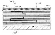
- FIG. 1is a cross-sectional schematic diagram of an inorganic/organic hybrid nanolaminate barrier film according to an embodiment of the present invention.
- Embodiments of the present inventionare directed to an inorganic/organic hybrid barrier nanolaminate film and methods for making the film.
- the film 100shown schematically in FIG. 1 , generally includes multiple alternating layers of organic material 102 and inorganic material 104 .
- the thickness of the inorganic layers 102 and organic layers 104can be from about 0.1 nm to about 1 nm or from about 1 nm to about 10 nm or from about 1 nm to about 100 nm.
- the inorganic layers 102can be silicates, although other inorganic materials can be formed from suitable alkoxides as described below.
- the barrier film 100can be made substantially transparent by appropriate choice of the number, thickness, and composition of the inorganic layers 102 and organic layers 104 . Although a relatively small number of layers is shown in FIG. 1 for the sake of clarity, a barrier film for a typical device can have many more layers, e.g., several thousand.
- the organic layers 104are polymers such as polyethylene naphthalate (PEN), polyether etherketone (PEEK), or polyether sulfone (PES).
- PENpolyethylene naphthalate
- PEEKpolyether etherketone
- PESpolyether sulfone
- polymers created from styrene polymer precursors, methyl styrene polymer precursors, (meth)acrylate polymer precursors, both fluorinated and non-fluorinated forms of these precursors, and combinations of two or more of these precursorscan be used as the organic layers 104 .
- These organic materialsare desirable because of their superior thermal properties and excellent gas barrier characteristics.
- one or more of the organic layers 104e.g., an uppermost layer 110 , may optionally be a superhydrophobic layer such as fluoroalkylsilane.
- Fluoroalkylsilane thin filmsare described, e.g., by Akira Nakajima et al., in “Transparent Superhydrophobic Thin Films with Self-Cleaning Properties”, Langmuir 2000, 16, 7044-7047, which is incorporated herein by reference.
- the layer structure of the barrier film 100provides a long path for water or oxygen to penetrate the barrier film to an underlying substrate 106 , e.g., via pinholes and/or gaps at interfaces between layers as indicated by the path 108 .
- the permeability of the nanolaminate barrier film 100 to oxygen and water vaporcan be adjusted by changing the number of layers. By using hundreds to thousands of interdigitated inorganic layers 102 and organic layers 104 within the barrier film 100 , the large number of layers combined with randomly located pinholes within the nanolaminate results in tortuous paths for molecules such as water vapor and oxygen that might enter from the environment outside of the barrier film 100 . The more layers, the more tortuous the path for permeating molecules. Thus, the more layers, the less permeable the barrier film 100 is to water vapor and oxygen. In embodiments of the present invention, there can be 100 or more, 1000 or more, 10,000 or more or 100,000 or more individual layers in the composite barrier film 100 .
- hydrophobic groupscan be incorporated into or eliminated from the polymer precursors used to form the organic layers 104 to tune (increase and/or decrease) the hydrophobicity of the resulting organic layers 104 and, in turn, adjust the permeability of the barrier film 100 .
- non-polar hydrophobic groupsincluding but not limited to methyl groups and benzyl (aromatic) groups, can be attached to the polymer precursors.
- increasing ionic strengthincreases hydrophobic interactions.
- the anions and cations listed beloware in a series from those that highly favor hydrophobic interactions to those that decrease hydrophobic interactions.
- any of these anions and/or cations and/or similar compoundscan be incorporated into the polymer precursors, resulting in polymers with tuned hydrophobicity.
- hydrophobic amino acidssuch as tryptophan, isoleucine, phenylalanine, tyrosine, leucine, valine, methionine, and alanine could be used as side chains for the polymer precursors.
- Gemini surfactantsare highly reactive and could be used as structure-directing agents. Gemini surfactants have two hydrophilic head groups and two hydrophobic groups in the molecule, in contrast to conventional surfactants that have only single hydrophilic and single hydrophobic groups.
- the oxygen permeability of the barrier film 100can be made less than about 1 cc/m 2 /day, 0.1 cc/m 2 /day, 0.01 cc/m 2 /day, 10 ⁇ 3 cc/m 2 /day, 10 ⁇ 4 cc/m 2 /day, 10 ⁇ 5 cc/m 2 /day, 10 ⁇ 6 cc/m 2 /day, or 10 ⁇ 7 cc/m 2 /day.
- the water vapor permeability of the barrier film 100can be made less than about 1 g/m 2 /day, 0.1 g/m 2 /day, 0.01 g/m 2 /day, 10 ⁇ 3 g/m 2 /day, 10 ⁇ 4 g/m 2 /day, 10 ⁇ 5 g/m 2 /day, 10 ⁇ 6 g/m 2 /day, or 10 ⁇ 7 g/m 2 /day.
- the nanolaminate barrier film 100can be made in a single-step (or few sequential step) process by self-assembly using sol-gel techniques.
- Self-assembly of nanocomposite materials using sol-gel techniquesis described, e.g., in U.S. Pat. No. 6,264,741 to Brinker et al., the entire contents of which are incorporated by reference.
- a solcan be prepared, e.g., by combining one or more alkoxides, an alcohol, water and dilute hydrochloric acid (HCl) and heating the resulting mixture.
- a coupling agentis then introduced to the mixture followed by a surfactant (or Gemini surfactant), in a quantity sufficient that the initial surfactant concentration is below the critical micelle concentration.
- a surfactantor Gemini surfactant
- one or more polymer precursorse.g., monomers suitable for the formation of PEN, PEEK or PES are then added followed by a cross-linker agent and an initiator.
- the polymer precursorscan include styrene polymer precursors, methyl styrene polymer precursors, (meth)acrylate polymer precursors, either fluorinated or non-fluorinated forms of these, precursors and combinations of two or more of these precursors.
- a substrateis coated with the sol and the alcohol is allowed to evaporate. The alcohol evaporation drives a self-assembly reaction that forms the multilayer barrier structure described with respect to FIG. 1 .
- Suitable alkoxidesare structured around a central element X.
- Suitable central elements Xinclude Al, B, Ba, Pb, Se, Si, and Sn.
- Other suitable central elements Xinclude transition metals, e.g., Ag, Au, Cd, Co, Cr, Cu, Fe, Ir, Mn, Mo, Nb, Ni, Sr, Ta, Ti, V, W, Y, Zn, Zr, etc.
- suitable alkoxidesinclude polysiloxanes such as tetraethylorthosilicate (TEOS).
- TEOStetraethylorthosilicate
- suitable alkoxidesinclude titanium ethoxide or titanium isopropoxide.
- a solcan be prepared, e.g., by combining tetraethylorthosilicate (Si(OCH 2 CH 3 ) 4 , also known as TEOS), ethanol, water and dilute HCl (dilute so as to minimize the siloxane condensation rate) in molar ratios of 1:3.8:1:5 ⁇ 10 ⁇ 5 respectively and heated at about 60° C. for about 90 minutes.
- the solis then diluted with ethanol in a 1:2 ration after which water and dilute HCl are added.
- a coupling agentsuch as 7-octenlytrimethoxysilane (OTS), or methacryloxypropyl trimethoxysilane (MPS) is then introduced to the mixture followed by a surfactant such as cetyltrimethylammonium bromide (CTAB) so that the initial surfactant concentration is below the critical micelle concentration.
- a surfactantsuch as cetyltrimethylammonium bromide (CTAB)
- a monomere.g., 2,6-Dimethylnaphthalene (DMN; to create polyethylene naphthalate (PEN)
- PENpolyethylene naphthalate
- B/FSdi-para-fluorophenylsulfone
- HDMhexanedioldimethacrylate
- BMEbenzoin dimethylether
- ACBN1,1′-azobis(1-cyclohexane carbonitrile
- the concentration of the surfactant, water, ethanol, TEOS, and organic monomerscan be varied. Annealing the films at about 125° C.-150° C. or greater (and/or below the decomposition temperature of the organic materials) further densifies the siloxane material and improves impermeability.
- the substrate 106can be coated with the sol mixture by any suitable technique, such as dip coating, spin coating, spray coating, web coating, or microgravure web coating.
- suitable coating machinesare commercially available, e.g., from Faustel, Inc., of Germantown, Wis.
- a Continuous Coater Type BA from Werner Mathis AG of Zurich, Switzerlandmay be used to coat the substrate with the sol mixture. It is desirable to coat the substrate with the sol in a wet layer approximately 1 microns to 10 microns to 100 microns thick. Thicker wet layers, e.g., about 100 microns to about 1 millimeter thick, can also be used. Since the barrier film 100 can be fabricated without the use of vacuum equipment, the processing is simple and comparatively low in cost.
- the substratecan be rapidly coated with the sol, e.g., by dip coating (e.g., about 25 cm/min dip and withdrawal rate; for large area substrates) or spin coating (e.g., about 1500 rpm for about 1 minute for small area substrates).
- dip coatinge.g., about 25 cm/min dip and withdrawal rate; for large area substrates
- spin coatinge.g., about 1500 rpm for about 1 minute for small area substrates.
- the ethanol component of the solbegins to evaporate, and the increasing concentrations of water and surfactant cause the surfactant concentration to exceed the critical micelle concentration, resulting in both micelle formation and the incorporation of the alcohol-soluble organic monomers into the micellar interiors.
- This TEOS and CTAB-based sol gel chemistryprovides for self-assembly of nanostructures whose chemical backbones condense into dense, stable materials.
- Evaporation-induced partitioningprovides a means to promote the co-dispersion of both organic and inorganic components throughout the nascent and emerging siloxane framework of the sol gel.
- the silica-surfactant-monomer micellesself-assemble into interfacially organized liquid crystal, lyotropic mesophases on a time scale of about 10 seconds.
- Polymerization of the organic material in the alternating interfacial layerscan be induced by either ultraviolet light or heat, which also stabilizes the polymerizing inorganic siloxane framework.
- the resulting nanocomposite structure in the multi-layer filmis stabilized by (a) organic polymerization, (b) inorganic polymerization, and (c) covalent bonding at the organic interfacial surfaces.
- a single coating stepcan produce films at least 1000 nm thick comprised of individual layers, each roughly 1 nm thick. By taking advantage of the self-assembling nature of the materials, each set of 1000 layers can be formed in only seconds. A greater number of layers in the resulting barrier film can be obtained by repeating the coating and evaporation sequence multiple times and/or by depositing thicker coatings.
- Conformal or non-conformal nanolaminate barrier coatings of the type described abovecan be applied to a variety of planar and non-planar surfaces, in two- and three-dimensions. More specifically, this nanolaminate approach could be used to encapsulate and or protect optoelectronic devices (e.g., LEDs, solar cells, FETs, lasers), pharmaceutical products (tablets in packages, etc), medical devices, food products (packaged foods, beverages, candies), display screens (touch panel displays, flat panel displays), and electroluminescent windows and other windows and transparent films and coatings, electronic components as well as the chassis for appliances used in rugged environments.
- optoelectronic devicese.g., LEDs, solar cells, FETs, lasers
- pharmaceutical productstablets in packages, etc
- medical devicese.g., food products (packaged foods, beverages, candies), display screens (touch panel displays, flat panel displays), and electroluminescent windows and other windows and transparent films and coatings, electronic components as well as the chassis for
- the nanolaminatecould be colored to provide for use as an optical filter in a variety of optoelectronic devices.
Landscapes
- Life Sciences & Earth Sciences (AREA)
- Engineering & Computer Science (AREA)
- Wood Science & Technology (AREA)
- Chemical & Material Sciences (AREA)
- Inorganic Chemistry (AREA)
- Physics & Mathematics (AREA)
- Optics & Photonics (AREA)
- Laminated Bodies (AREA)
- Application Of Or Painting With Fluid Materials (AREA)
- Silicates, Zeolites, And Molecular Sieves (AREA)
- Photovoltaic Devices (AREA)
- Electroluminescent Light Sources (AREA)
Abstract
Description
- The present invention is directed to barrier films and more particularly to multilayer barrier coatings.
- Many products that are sensitive to their environment require a barrier that is highly impermeable to water, oxygen and other gases while remaining lightweight and durable. For example, optoelectronic devices require transparent barrier materials to extend their useful operating lives. Currently, glass is used as a transparent barrier material. Unfortunately, glass is often undesirable because it is either too fragile or too heavy or both. Plastics are more lightweight and less fragile materials. Unfortunately, commercially available plastics lack the desired level of environmental resistance for many optoelectronic applications.
- For example, to build durable devices, the active elements of polymer-based LEDs may require incorporation of barrier layers with oxygen permeability levels as low as 10−5cc/m2/day and water vapor permeability levels as low as 10−6g/m2/day. A 7 mil thick coating of polyethylene teraphthalate (PET) has an oxygen transmission rate of 8.7 cc/m2/day and a water vapor permeability of 10 g/m2/day. State of the art plastics such as Alcar can protect components with oxygen and water vapor permeability levels of about 7 cc/m2/day and 0.016 g/m2/day respectively.
- Single barrier coatings of thin films of inorganic materials such as Al, SiO2Al2O3and Si3N4can be vacuum deposited on polymer substrates to improve barrier impermeability. Such single layer coatings can reduce oxygen and water vapor permeability to levels of about 10−3cc/m2/day and 10−3g/m2/day respectively.
- Multilayer barrier coatings have been developed using a “sandwich” strategy with an inorganic layer is situated between two polymer layers to further improve the aggregate barrier properties. Sheats and coworkers (U.S. Pat. No. 6,146,225) used a 35 nm thick silicon nitride as an inorganic layer and a one micron thick layer of an acrylate as the polymer material to achieve a barrier with a water-vapor permeation rate of 1.8×10⁻⁷g/m2/day, which is about 40 times better than the requirement for most optoelectronic devices. However, this material is not optically transparent, limiting its use to certain applications only.
- More recently, Graff and colleagues (U.S. Pat. No. 6,413,645; U.S. Pat. No. 6,573,652 and U.S. Pat. No. 6,623,861) have developed barrier materials using a multi-stack approach where each stack includes a sputter-deposited, 40 nm barrier layer of a metal oxide, metal nitride, or metal carbide, followed by a flash-evaporated, one micron layer of an acrylate polymer or multilayer thin films comprised of flash-evaporated plastic. While these multi-stack barrier films have useful environmental resistance relative to many previously developed materials, their vacuum-based mode of production is time-consuming and relatively expensive, especially for multiple-stack coatings. Further, the vacuum-based deposition methods limit both the area upon which a coating can be placed (the area must be smaller than the deposition chamber), which in turn limits their use for larger area devices. In addition, flash evaporation and sputter deposition do not tend to provide for uniform conformal coatings of large area surfaces, especially for non-planar substrates with inherent curvature (or even three-dimensional barrier-protection targets). It would be desirable to have a multi-layer, transparent, and durable film that provides for uniform, inexpensive and conformal coating of larger areas with effective environmental resistance in a range of environments.
- Thus, there is a need in the art, for a barrier film that overcomes the above disadvantages and a corresponding method for making such a film.
- The teachings of the present invention can be readily understood by considering the following detailed description in conjunction with the accompanying drawings, in which:
FIG. 1 is a cross-sectional schematic diagram of an inorganic/organic hybrid nanolaminate barrier film according to an embodiment of the present invention.- Although the following detailed description contains many specific details for the purposes of illustration, anyone of ordinary skill in the art will appreciate that many variations and alterations to the following details are within the scope of the invention. Accordingly, the exemplary embodiments of the invention described below are set forth without any loss of generality to, and without imposing limitations upon, the claimed invention.
- Embodiments of the present invention are directed to an inorganic/organic hybrid barrier nanolaminate film and methods for making the film. The
film 100, shown schematically inFIG. 1 , generally includes multiple alternating layers oforganic material 102 andinorganic material 104. The thickness of theinorganic layers 102 andorganic layers 104 can be from about 0.1 nm to about 1 nm or from about 1 nm to about 10 nm or from about 1 nm to about 100 nm. Theinorganic layers 102 can be silicates, although other inorganic materials can be formed from suitable alkoxides as described below. Thebarrier film 100 can be made substantially transparent by appropriate choice of the number, thickness, and composition of theinorganic layers 102 andorganic layers 104. Although a relatively small number of layers is shown inFIG. 1 for the sake of clarity, a barrier film for a typical device can have many more layers, e.g., several thousand. - The
organic layers 104 are polymers such as polyethylene naphthalate (PEN), polyether etherketone (PEEK), or polyether sulfone (PES). In addition, polymers created from styrene polymer precursors, methyl styrene polymer precursors, (meth)acrylate polymer precursors, both fluorinated and non-fluorinated forms of these precursors, and combinations of two or more of these precursors can be used as theorganic layers 104. These organic materials are desirable because of their superior thermal properties and excellent gas barrier characteristics. Furthermore, one or more of theorganic layers 104, e.g., anuppermost layer 110, may optionally be a superhydrophobic layer such as fluoroalkylsilane. Fluoroalkylsilane thin films are described, e.g., by Akira Nakajima et al., in “Transparent Superhydrophobic Thin Films with Self-Cleaning Properties”, Langmuir 2000, 16, 7044-7047, which is incorporated herein by reference. - The layer structure of the
barrier film 100 provides a long path for water or oxygen to penetrate the barrier film to anunderlying substrate 106, e.g., via pinholes and/or gaps at interfaces between layers as indicated by thepath 108. The permeability of thenanolaminate barrier film 100 to oxygen and water vapor can be adjusted by changing the number of layers. By using hundreds to thousands of interdigitatedinorganic layers 102 andorganic layers 104 within thebarrier film 100, the large number of layers combined with randomly located pinholes within the nanolaminate results in tortuous paths for molecules such as water vapor and oxygen that might enter from the environment outside of thebarrier film 100. The more layers, the more tortuous the path for permeating molecules. Thus, the more layers, the less permeable thebarrier film 100 is to water vapor and oxygen. In embodiments of the present invention, there can be 100 or more, 1000 or more, 10,000 or more or 100,000 or more individual layers in thecomposite barrier film 100. - Furthermore, hydrophobic groups can be incorporated into or eliminated from the polymer precursors used to form the
organic layers 104 to tune (increase and/or decrease) the hydrophobicity of the resultingorganic layers 104 and, in turn, adjust the permeability of thebarrier film 100. For example, non-polar hydrophobic groups, including but not limited to methyl groups and benzyl (aromatic) groups, can be attached to the polymer precursors. In general, increasing ionic strength increases hydrophobic interactions. For example, the anions and cations listed below are in a series from those that highly favor hydrophobic interactions to those that decrease hydrophobic interactions. - Anions: PO43−, SO42−, CH3COO−, Cl−, Br−, NO−, ClO4−, I−, SCn−.
- Cations: NH4+, Rb+, K+, Na+, Cs+, Li+, Mg2+, Ca2+, Ba2+.
- Any of these anions and/or cations and/or similar compounds can be incorporated into the polymer precursors, resulting in polymers with tuned hydrophobicity.
- In addition, hydrophobic amino acids such as tryptophan, isoleucine, phenylalanine, tyrosine, leucine, valine, methionine, and alanine could be used as side chains for the polymer precursors.
- Furthermore, Gemini surfactants (also called dimeric surfactants) are highly reactive and could be used as structure-directing agents. Gemini surfactants have two hydrophilic head groups and two hydrophobic groups in the molecule, in contrast to conventional surfactants that have only single hydrophilic and single hydrophobic groups.
- By suitable choice of the number and composition of layers, the oxygen permeability of the
barrier film 100 can be made less than about 1 cc/m2/day, 0.1 cc/m2/day, 0.01 cc/m2/day, 10−3cc/m2/day, 10−4cc/m2/day, 10−5cc/m2/day, 10−6cc/m2/day, or 10−7cc/m2/day. Similarly, the water vapor permeability of thebarrier film 100 can be made less than about 1 g/m2/day, 0.1 g/m2/day, 0.01 g/m2/day, 10−3g/m2/day, 10−4g/m2/day, 10−5g/m2/day, 10−6g/m2/day, or 10−7g/m2/day. - The
nanolaminate barrier film 100 can be made in a single-step (or few sequential step) process by self-assembly using sol-gel techniques. Self-assembly of nanocomposite materials using sol-gel techniques is described, e.g., in U.S. Pat. No. 6,264,741 to Brinker et al., the entire contents of which are incorporated by reference. Generally speaking, a sol can be prepared, e.g., by combining one or more alkoxides, an alcohol, water and dilute hydrochloric acid (HCl) and heating the resulting mixture. A coupling agent is then introduced to the mixture followed by a surfactant (or Gemini surfactant), in a quantity sufficient that the initial surfactant concentration is below the critical micelle concentration. Subsequently, one or more polymer precursors, e.g., monomers suitable for the formation of PEN, PEEK or PES are then added followed by a cross-linker agent and an initiator. Alternatively, the polymer precursors can include styrene polymer precursors, methyl styrene polymer precursors, (meth)acrylate polymer precursors, either fluorinated or non-fluorinated forms of these, precursors and combinations of two or more of these precursors. A substrate is coated with the sol and the alcohol is allowed to evaporate. The alcohol evaporation drives a self-assembly reaction that forms the multilayer barrier structure described with respect toFIG. 1 . - Suitable alkoxides are structured around a central element X. Suitable central elements X include Al, B, Ba, Pb, Se, Si, and Sn. Other suitable central elements X include transition metals, e.g., Ag, Au, Cd, Co, Cr, Cu, Fe, Ir, Mn, Mo, Nb, Ni, Sr, Ta, Ti, V, W, Y, Zn, Zr, etc.
- For silicon (Si)-based
inorganic layers 102 examples of suitable alkoxides include polysiloxanes such as tetraethylorthosilicate (TEOS). For titanium (Ti)-basedinorganic layers 102 examples of suitable alkoxides include titanium ethoxide or titanium isopropoxide. - Sol Preparation and Tuning
- By way of example, and without loss of generality, a sol can be prepared, e.g., by combining tetraethylorthosilicate (Si(OCH2CH3)4, also known as TEOS), ethanol, water and dilute HCl (dilute so as to minimize the siloxane condensation rate) in molar ratios of 1:3.8:1:5×10⁻⁵respectively and heated at about 60° C. for about 90 minutes. The sol is then diluted with ethanol in a 1:2 ration after which water and dilute HCl are added. A coupling agent such as 7-octenlytrimethoxysilane (OTS), or methacryloxypropyl trimethoxysilane (MPS) is then introduced to the mixture followed by a surfactant such as cetyltrimethylammonium bromide (CTAB) so that the initial surfactant concentration is below the critical micelle concentration. After stirring for about one hour, a monomer (e.g., 2,6-Dimethylnaphthalene (DMN; to create polyethylene naphthalate (PEN)), or a set of monomers such as bisphenol A and di-para-fluorophenylsulfone (B/FS, to create polyether sulfone (PES)) is then added followed by a cross-linker agent (such as hexanedioldimethacrylate (HDM) and an initiator. For ultraviolet initiation benzoin dimethylether (BME), can be added. For thermal initiation, 1,1′-azobis(1-cyclohexane carbonitrile) (ACHN) can be used).
- To tune the chemistry of the sol, the concentration of the surfactant, water, ethanol, TEOS, and organic monomers can be varied. Annealing the films at about 125° C.-150° C. or greater (and/or below the decomposition temperature of the organic materials) further densifies the siloxane material and improves impermeability.
- Coating and Nanolaminate Self-Assembly
- The
substrate 106 can be coated with the sol mixture by any suitable technique, such as dip coating, spin coating, spray coating, web coating, or microgravure web coating. Suitable coating machines are commercially available, e.g., from Faustel, Inc., of Germantown, Wis. In particular, a Continuous Coater Type BA from Werner Mathis AG of Zurich, Switzerland may be used to coat the substrate with the sol mixture. It is desirable to coat the substrate with the sol in a wet layer approximately 1 microns to 10 microns to 100 microns thick. Thicker wet layers, e.g., about 100 microns to about 1 millimeter thick, can also be used. Since thebarrier film 100 can be fabricated without the use of vacuum equipment, the processing is simple and comparatively low in cost. - By way of example, the substrate can be rapidly coated with the sol, e.g., by dip coating (e.g., about 25 cm/min dip and withdrawal rate; for large area substrates) or spin coating (e.g., about 1500 rpm for about 1 minute for small area substrates). After coating, the ethanol component of the sol begins to evaporate, and the increasing concentrations of water and surfactant cause the surfactant concentration to exceed the critical micelle concentration, resulting in both micelle formation and the incorporation of the alcohol-soluble organic monomers into the micellar interiors. This TEOS and CTAB-based sol gel chemistry provides for self-assembly of nanostructures whose chemical backbones condense into dense, stable materials.
- Evaporation-induced partitioning provides a means to promote the co-dispersion of both organic and inorganic components throughout the nascent and emerging siloxane framework of the sol gel. As the ethanol continues to evaporate, the silica-surfactant-monomer micelles self-assemble into interfacially organized liquid crystal, lyotropic mesophases on a time scale of about 10 seconds. Polymerization of the organic material in the alternating interfacial layers can be induced by either ultraviolet light or heat, which also stabilizes the polymerizing inorganic siloxane framework. The resulting nanocomposite structure in the multi-layer film is stabilized by (a) organic polymerization, (b) inorganic polymerization, and (c) covalent bonding at the organic interfacial surfaces. A single coating step can produce films at least 1000 nm thick comprised of individual layers, each roughly 1 nm thick. By taking advantage of the self-assembling nature of the materials, each set of 1000 layers can be formed in only seconds. A greater number of layers in the resulting barrier film can be obtained by repeating the coating and evaporation sequence multiple times and/or by depositing thicker coatings.
- Options and Alternative Embodiments
- Conformal or non-conformal nanolaminate barrier coatings of the type described above can be applied to a variety of planar and non-planar surfaces, in two- and three-dimensions. More specifically, this nanolaminate approach could be used to encapsulate and or protect optoelectronic devices (e.g., LEDs, solar cells, FETs, lasers), pharmaceutical products (tablets in packages, etc), medical devices, food products (packaged foods, beverages, candies), display screens (touch panel displays, flat panel displays), and electroluminescent windows and other windows and transparent films and coatings, electronic components as well as the chassis for appliances used in rugged environments.
- Furthermore, by incorporating dyes or pigments into the film, the nanolaminate could be colored to provide for use as an optical filter in a variety of optoelectronic devices.
- While the above is a complete description of the preferred embodiment of the present invention, it is possible to use various alternatives, modifications and equivalents. Therefore, the scope of the present invention should be determined not with reference to the above description but should, instead, be determined with reference to the appended claims, along with their full scope of equivalents. The appended claims are not to be interpreted as including means-plus-function limitations, unless such a limitation is explicitly recited in a given claim using the phrase “means for.”
Claims (24)
Priority Applications (7)
| Application Number | Priority Date | Filing Date | Title |
|---|---|---|---|
| US10/698,988US8722160B2 (en) | 2003-10-31 | 2003-10-31 | Inorganic/organic hybrid nanolaminate barrier film |
| JP2006538120AJP5703431B2 (en) | 2003-10-31 | 2004-10-18 | Method for forming inorganic / organic hybrid nanolaminate barrier film |
| TW093131587ATWI376825B (en) | 2003-10-31 | 2004-10-18 | Inorganic/organic hybrid nanolaminate barrier film |
| PCT/US2004/034993WO2005044551A1 (en) | 2003-10-31 | 2004-10-18 | Inorganic/organic hybrid nanolaminate barrier film |
| EP04796054AEP1682339A4 (en) | 2003-10-31 | 2004-10-18 | Inorganic/organic hybrid nanolaminate barrier film |
| JP2013185134AJP2013256132A (en) | 2003-10-31 | 2013-09-06 | Inorganic/organic hybrid nanolaminate barrier film |
| US14/274,527US20140314958A1 (en) | 2003-10-31 | 2014-05-09 | Inorganic/organic hybrid nanolaminate barrier film |
Applications Claiming Priority (1)
| Application Number | Priority Date | Filing Date | Title |
|---|---|---|---|
| US10/698,988US8722160B2 (en) | 2003-10-31 | 2003-10-31 | Inorganic/organic hybrid nanolaminate barrier film |
Related Child Applications (1)
| Application Number | Title | Priority Date | Filing Date |
|---|---|---|---|
| US14/274,527DivisionUS20140314958A1 (en) | 2003-10-31 | 2014-05-09 | Inorganic/organic hybrid nanolaminate barrier film |
Publications (2)
| Publication Number | Publication Date |
|---|---|
| US20050095422A1true US20050095422A1 (en) | 2005-05-05 |
| US8722160B2 US8722160B2 (en) | 2014-05-13 |
Family
ID=34550810
Family Applications (2)
| Application Number | Title | Priority Date | Filing Date |
|---|---|---|---|
| US10/698,988Expired - Fee RelatedUS8722160B2 (en) | 2003-10-31 | 2003-10-31 | Inorganic/organic hybrid nanolaminate barrier film |
| US14/274,527AbandonedUS20140314958A1 (en) | 2003-10-31 | 2014-05-09 | Inorganic/organic hybrid nanolaminate barrier film |
Family Applications After (1)
| Application Number | Title | Priority Date | Filing Date |
|---|---|---|---|
| US14/274,527AbandonedUS20140314958A1 (en) | 2003-10-31 | 2014-05-09 | Inorganic/organic hybrid nanolaminate barrier film |
Country Status (5)
| Country | Link |
|---|---|
| US (2) | US8722160B2 (en) |
| EP (1) | EP1682339A4 (en) |
| JP (2) | JP5703431B2 (en) |
| TW (1) | TWI376825B (en) |
| WO (1) | WO2005044551A1 (en) |
Cited By (52)
| Publication number | Priority date | Publication date | Assignee | Title |
|---|---|---|---|---|
| US20050271893A1 (en)* | 2004-06-04 | 2005-12-08 | Applied Microstructures, Inc. | Controlled vapor deposition of multilayered coatings adhered by an oxide layer |
| US20050271810A1 (en)* | 2004-06-04 | 2005-12-08 | Boris Kobrin | High aspect ratio performance coatings for biological microfluidics |
| US20060157103A1 (en)* | 2005-01-20 | 2006-07-20 | Nanosolar, Inc. | Optoelectronic architecture having compound conducting substrate cross-reference to related application |
| US20060275950A1 (en)* | 2005-06-01 | 2006-12-07 | Woo-Jae Lee | Method of manufacturing a flexible display device |
| US20070005024A1 (en)* | 2005-06-10 | 2007-01-04 | Jan Weber | Medical devices having superhydrophobic surfaces, superhydrophilic surfaces, or both |
| US20070020392A1 (en)* | 2004-06-04 | 2007-01-25 | Applied Microstructures, Inc. | Functional organic based vapor deposited coatings adhered by an oxide layer |
| US7227066B1 (en)* | 2004-04-21 | 2007-06-05 | Nanosolar, Inc. | Polycrystalline optoelectronic devices based on templating technique |
| US20070157968A1 (en)* | 2006-01-12 | 2007-07-12 | Stanbery Billy J | Compositions including controlled segregated phase domain structures |
| US20070160763A1 (en)* | 2006-01-12 | 2007-07-12 | Stanbery Billy J | Methods of making controlled segregated phase domain structures |
| US20070160770A1 (en)* | 2006-01-12 | 2007-07-12 | Stanbery Billy J | Apparatus for making controlled segregated phase domain structures |
| KR100763933B1 (en) | 2006-07-11 | 2007-10-05 | 인하대학교 산학협력단 | Process for preparing organic-inorganic hybrid material |
| US20080017242A1 (en)* | 2006-04-21 | 2008-01-24 | Sanjai Sinha | Group iv nanoparticles in an oxide matrix and devices made therefrom |
| US20080070034A1 (en)* | 2006-09-20 | 2008-03-20 | Battelle Memorial Institute | Nanostructured thin film optical coatings |
| US20080311028A1 (en)* | 2007-06-18 | 2008-12-18 | Stanbery Billy J | Assemblies of anisotropic nanoparticles |
| US20090032108A1 (en)* | 2007-03-30 | 2009-02-05 | Craig Leidholm | Formation of photovoltaic absorber layers on foil substrates |
| US20090079934A1 (en)* | 2007-09-24 | 2009-03-26 | Qspex Technologies, Inc. | Method for manufacturing polarized ophthalmic lenses |
| US7510913B2 (en) | 2003-04-11 | 2009-03-31 | Vitex Systems, Inc. | Method of making an encapsulated plasma sensitive device |
| USRE40787E1 (en) | 1999-10-25 | 2009-06-23 | Battelle Memorial Institute | Multilayer plastic substrates |
| US20090233108A1 (en)* | 2008-03-17 | 2009-09-17 | Naoki Tsukamoto | Vacuum film formation method for inorganic layer, barrier laminate, device, and optical component |
| US20100031997A1 (en)* | 2008-08-11 | 2010-02-11 | Basol Bulent M | Flexible thin film photovoltaic modules and manufacturing the same |
| US20100129545A1 (en)* | 2008-11-21 | 2010-05-27 | Buck Thomas Lavee | Method Of Coating Tubes Using A Self-Assembly Process |
| US20100151209A1 (en)* | 2008-12-15 | 2010-06-17 | Industrial Technology Research Institute | Organic/inorganic multi-layered gas barrier film |
| US7767498B2 (en) | 2005-08-25 | 2010-08-03 | Vitex Systems, Inc. | Encapsulated devices and method of making |
| US7772487B1 (en) | 2004-10-16 | 2010-08-10 | Nanosolar, Inc. | Photovoltaic cell with enhanced energy transfer |
| US20100258180A1 (en)* | 2009-02-04 | 2010-10-14 | Yuepeng Deng | Method of forming an indium-containing transparent conductive oxide film, metal targets used in the method and photovoltaic devices utilizing said films |
| US20100310770A1 (en)* | 2009-06-05 | 2010-12-09 | Baosheng Sang | Process for synthesizing a thin film or composition layer via non-contact pressure containment |
| US20100315353A1 (en)* | 2009-06-12 | 2010-12-16 | Au Optronics Corp. | Flexible Touch Display Apparatus |
| US20110062049A1 (en)* | 2009-09-11 | 2011-03-17 | Pro-Pak Industries, Inc. | Load tray and method for unitizing a palletized load |
| US20110189080A1 (en)* | 2010-02-04 | 2011-08-04 | Curtis Calvin J | Methods of making copper selenium precursor compositions with a targeted copper selenide content and precursor compositions and thin films resulting therefrom |
| US20120052244A1 (en)* | 2009-05-05 | 2012-03-01 | Fraunhofer-Gesellschaft Zur Foerderung Der Angewandten Forschung E.V. | Layer system having barrier properties and a structured conductive layer, method for producing the same, and use of such a layer system |
| US8158450B1 (en) | 2006-05-05 | 2012-04-17 | Nanosolar, Inc. | Barrier films and high throughput manufacturing processes for photovoltaic devices |
| US8418418B2 (en) | 2009-04-29 | 2013-04-16 | 3Form, Inc. | Architectural panels with organic photovoltaic interlayers and methods of forming the same |
| US8590338B2 (en) | 2009-12-31 | 2013-11-26 | Samsung Mobile Display Co., Ltd. | Evaporator with internal restriction |
| US20140150843A1 (en)* | 2011-04-01 | 2014-06-05 | NuvoSun, Inc. | Shingle-like photovoltaic modules |
| EP2706612A3 (en)* | 2012-09-05 | 2014-07-02 | Raytheon Company | Radome film |
| US8808457B2 (en) | 2002-04-15 | 2014-08-19 | Samsung Display Co., Ltd. | Apparatus for depositing a multilayer coating on discrete sheets |
| CN104037352A (en)* | 2013-03-07 | 2014-09-10 | 海洋王照明科技股份有限公司 | Organic light emission diode and preparation method thereof |
| US20140349422A1 (en)* | 2011-02-08 | 2014-11-27 | Applied Materials, Inc. | Method for hybrid encapsulation of an organic light emitting diode |
| US8900366B2 (en) | 2002-04-15 | 2014-12-02 | Samsung Display Co., Ltd. | Apparatus for depositing a multilayer coating on discrete sheets |
| US8927315B1 (en) | 2005-01-20 | 2015-01-06 | Aeris Capital Sustainable Ip Ltd. | High-throughput assembly of series interconnected solar cells |
| US8955217B2 (en) | 1999-10-25 | 2015-02-17 | Samsung Display Co., Ltd. | Method for edge sealing barrier films |
| US9105797B2 (en) | 2012-05-31 | 2015-08-11 | Alliance For Sustainable Energy, Llc | Liquid precursor inks for deposition of In—Se, Ga—Se and In—Ga—Se |
| US9130084B2 (en) | 2010-05-21 | 2015-09-08 | Alliance for Substainable Energy, LLC | Liquid precursor for deposition of copper selenide and method of preparing the same |
| US9142408B2 (en) | 2010-08-16 | 2015-09-22 | Alliance For Sustainable Energy, Llc | Liquid precursor for deposition of indium selenide and method of preparing the same |
| US9184410B2 (en) | 2008-12-22 | 2015-11-10 | Samsung Display Co., Ltd. | Encapsulated white OLEDs having enhanced optical output |
| US9337446B2 (en) | 2008-12-22 | 2016-05-10 | Samsung Display Co., Ltd. | Encapsulated RGB OLEDs having enhanced optical output |
| CN105593797A (en)* | 2013-09-30 | 2016-05-18 | 凸版印刷株式会社 | Touch panel |
| WO2017215544A1 (en)* | 2016-06-14 | 2017-12-21 | 中国科学院理化技术研究所 | Preparation method for hydrophobic inorganic powder material |
| CN109888128A (en)* | 2019-03-25 | 2019-06-14 | 京东方科技集团股份有限公司 | OLED display panel packaging method and display panel manufacturing method |
| WO2019114574A1 (en)* | 2017-12-15 | 2019-06-20 | Boe Technology Group Co., Ltd. | Display component packaging assembly, manufacturing method thereof, and display apparatus |
| US10730790B2 (en) | 2015-02-25 | 2020-08-04 | Corning Incorporated | Optical structures and articles with multilayer stacks having high hardness and methods for making the same |
| US10950821B2 (en) | 2007-01-26 | 2021-03-16 | Samsung Display Co., Ltd. | Method of encapsulating an environmentally sensitive device |
Families Citing this family (15)
| Publication number | Priority date | Publication date | Assignee | Title |
|---|---|---|---|---|
| US8722160B2 (en)* | 2003-10-31 | 2014-05-13 | Aeris Capital Sustainable Ip Ltd. | Inorganic/organic hybrid nanolaminate barrier film |
| FR2956869B1 (en) | 2010-03-01 | 2014-05-16 | Alex Hr Roustaei | SYSTEM FOR PRODUCING HIGH CAPACITY FLEXIBLE FILM FOR PHOTOVOLTAIC AND OLED CELLS BY CYCLIC LAYER DEPOSITION |
| KR101891987B1 (en)* | 2011-05-31 | 2018-08-28 | 엘지디스플레이 주식회사 | Organic Light Emitting Device and Method for manufacturing the same |
| DE102011056761A1 (en) | 2011-12-21 | 2013-08-08 | Leibniz-Institut Für Neue Materialien Gemeinnützige Gmbh | Pigmented, finely structured tribological composite material |
| WO2013091685A1 (en) | 2011-12-21 | 2013-06-27 | Leibniz-Institut Für Neue Materialien Gemeinnützige Gmbh | Highly structured composite material and process for the manufacture of protective coatings for corroding substrates |
| US20140370217A1 (en) | 2011-12-21 | 2014-12-18 | Tenaris Connections Limited | Corrosion Resistant Equipment for Oil and/or Gas Applications |
| CN103374138A (en)* | 2012-04-25 | 2013-10-30 | 深圳富泰宏精密工业有限公司 | Shell and preparation method thereof |
| JP6946185B2 (en)* | 2014-11-17 | 2021-10-06 | セイジ・エレクトロクロミクス,インコーポレイテッド | Multiple barrier layer sealed laminate |
| KR102421600B1 (en) | 2015-11-20 | 2022-07-18 | 삼성디스플레이 주식회사 | Touch sensing unit, display device and fabrication method of the touch screen |
| KR102127463B1 (en)* | 2017-08-18 | 2020-06-29 | 한국과학기술원 | Encapsulation structure for transparent flexible organic electronic device |
| US10529951B2 (en) | 2017-08-18 | 2020-01-07 | Korea Advanced Institute Of Science And Technology | Encapsulation structure for transparent flexible organic electronic device |
| KR102578827B1 (en) | 2018-04-24 | 2023-09-15 | 삼성전자주식회사 | Flexible organic-inorganic passivation layer an method of fabricating the same |
| CN109950418A (en)* | 2019-03-18 | 2019-06-28 | 云谷(固安)科技有限公司 | Display panel and display screen |
| KR102417793B1 (en)* | 2020-12-15 | 2022-07-14 | 포항공과대학교 산학협력단 | Composition for an organic-inorganic hybrid gas barrier film containing a fluorine-based precursor and amphiphilic legged structured polymeric alkoxysilane precursor and a gas barrier film using the same |
| CN117812931B (en)* | 2023-12-27 | 2025-02-11 | 惠科股份有限公司 | Method for manufacturing display panel, display panel and display device |
Citations (14)
| Publication number | Priority date | Publication date | Assignee | Title |
|---|---|---|---|---|
| US4869755A (en)* | 1987-07-30 | 1989-09-26 | Nukem Gmbh | Encapsulation of a photovoltaic element |
| US5372888A (en)* | 1991-02-06 | 1994-12-13 | Matsushita Electric Industrial Co., Ltd. | Chemically adsorbed film and method of manufacturing the same |
| US5554670A (en)* | 1994-09-12 | 1996-09-10 | Cornell Research Foundation, Inc. | Method of preparing layered silicate-epoxy nanocomposites |
| US6057035A (en)* | 1997-06-06 | 2000-05-02 | Triton Systems, Inc. | High-temperature polymer/inorganic nanocomposites |
| US6133522A (en)* | 1997-08-27 | 2000-10-17 | Canon Kabushiki Kaisha | Solar cell module and reinforcing member for solar cell module |
| US6146224A (en)* | 1996-01-11 | 2000-11-14 | Mccarthy; Peter T. | High efficiency hydrofoil and swim fin designs |
| US6264741B1 (en)* | 1998-11-25 | 2001-07-24 | Sandia Corporation | Self-assembly of nanocomposite materials |
| US6413645B1 (en)* | 2000-04-20 | 2002-07-02 | Battelle Memorial Institute | Ultrabarrier substrates |
| US6472467B1 (en)* | 1999-10-21 | 2002-10-29 | Dow Global Technologies Inc. | Inorganic/organic compositions |
| US6573652B1 (en)* | 1999-10-25 | 2003-06-03 | Battelle Memorial Institute | Encapsulated display devices |
| US6623861B2 (en)* | 2001-04-16 | 2003-09-23 | Battelle Memorial Institute | Multilayer plastic substrates |
| US6727513B2 (en)* | 2000-03-31 | 2004-04-27 | Seiko Epson Corporation | Method of manufacturing organic EL element |
| US6818163B1 (en)* | 1999-02-12 | 2004-11-16 | Dow Global Technologies Inc. | Nanocomposite articles and process for making |
| US6866901B2 (en)* | 1999-10-25 | 2005-03-15 | Vitex Systems, Inc. | Method for edge sealing barrier films |
Family Cites Families (9)
| Publication number | Priority date | Publication date | Assignee | Title |
|---|---|---|---|---|
| JPS5947987B2 (en)* | 1979-10-08 | 1984-11-22 | 富士写真フイルム株式会社 | Matsuto film that can be added/edited |
| DE3884435T2 (en)* | 1987-03-25 | 1994-02-17 | Hitachi Ltd | Processes for producing high-purity water and process for using this water. |
| JPH07270615A (en) | 1994-03-31 | 1995-10-20 | Central Glass Co Ltd | Holographic laminated body |
| US6146225A (en) | 1998-07-30 | 2000-11-14 | Agilent Technologies, Inc. | Transparent, flexible permeability barrier for organic electroluminescent devices |
| WO2000078540A1 (en)* | 1999-06-17 | 2000-12-28 | Triton Systems, Inc. | High performance nanocomposites |
| CA2404013A1 (en)* | 2000-04-21 | 2001-11-01 | Hongyou Fan | Prototyping of patterned functional nanostructures |
| DE60127527T2 (en)* | 2001-01-19 | 2007-12-13 | 3M Innovative Properties Co., St. Paul | Water-soluble or water-dispersible fluorochemical silanes to make substrates oil and water repellent |
| US20040168627A1 (en)* | 2003-02-27 | 2004-09-02 | Sharp Laboratories Of America, Inc. | Atomic layer deposition of oxide film |
| US8722160B2 (en)* | 2003-10-31 | 2014-05-13 | Aeris Capital Sustainable Ip Ltd. | Inorganic/organic hybrid nanolaminate barrier film |
- 2003
- 2003-10-31USUS10/698,988patent/US8722160B2/ennot_activeExpired - Fee Related
- 2004
- 2004-10-18EPEP04796054Apatent/EP1682339A4/ennot_activeWithdrawn
- 2004-10-18JPJP2006538120Apatent/JP5703431B2/ennot_activeExpired - Fee Related
- 2004-10-18TWTW093131587Apatent/TWI376825B/enactive
- 2004-10-18WOPCT/US2004/034993patent/WO2005044551A1/enactiveApplication Filing
- 2013
- 2013-09-06JPJP2013185134Apatent/JP2013256132A/enactivePending
- 2014
- 2014-05-09USUS14/274,527patent/US20140314958A1/ennot_activeAbandoned
Patent Citations (14)
| Publication number | Priority date | Publication date | Assignee | Title |
|---|---|---|---|---|
| US4869755A (en)* | 1987-07-30 | 1989-09-26 | Nukem Gmbh | Encapsulation of a photovoltaic element |
| US5372888A (en)* | 1991-02-06 | 1994-12-13 | Matsushita Electric Industrial Co., Ltd. | Chemically adsorbed film and method of manufacturing the same |
| US5554670A (en)* | 1994-09-12 | 1996-09-10 | Cornell Research Foundation, Inc. | Method of preparing layered silicate-epoxy nanocomposites |
| US6146224A (en)* | 1996-01-11 | 2000-11-14 | Mccarthy; Peter T. | High efficiency hydrofoil and swim fin designs |
| US6057035A (en)* | 1997-06-06 | 2000-05-02 | Triton Systems, Inc. | High-temperature polymer/inorganic nanocomposites |
| US6133522A (en)* | 1997-08-27 | 2000-10-17 | Canon Kabushiki Kaisha | Solar cell module and reinforcing member for solar cell module |
| US6264741B1 (en)* | 1998-11-25 | 2001-07-24 | Sandia Corporation | Self-assembly of nanocomposite materials |
| US6818163B1 (en)* | 1999-02-12 | 2004-11-16 | Dow Global Technologies Inc. | Nanocomposite articles and process for making |
| US6472467B1 (en)* | 1999-10-21 | 2002-10-29 | Dow Global Technologies Inc. | Inorganic/organic compositions |
| US6573652B1 (en)* | 1999-10-25 | 2003-06-03 | Battelle Memorial Institute | Encapsulated display devices |
| US6866901B2 (en)* | 1999-10-25 | 2005-03-15 | Vitex Systems, Inc. | Method for edge sealing barrier films |
| US6727513B2 (en)* | 2000-03-31 | 2004-04-27 | Seiko Epson Corporation | Method of manufacturing organic EL element |
| US6413645B1 (en)* | 2000-04-20 | 2002-07-02 | Battelle Memorial Institute | Ultrabarrier substrates |
| US6623861B2 (en)* | 2001-04-16 | 2003-09-23 | Battelle Memorial Institute | Multilayer plastic substrates |
Cited By (83)
| Publication number | Priority date | Publication date | Assignee | Title |
|---|---|---|---|---|
| US8955217B2 (en) | 1999-10-25 | 2015-02-17 | Samsung Display Co., Ltd. | Method for edge sealing barrier films |
| USRE40787E1 (en) | 1999-10-25 | 2009-06-23 | Battelle Memorial Institute | Multilayer plastic substrates |
| US8808457B2 (en) | 2002-04-15 | 2014-08-19 | Samsung Display Co., Ltd. | Apparatus for depositing a multilayer coating on discrete sheets |
| US8900366B2 (en) | 2002-04-15 | 2014-12-02 | Samsung Display Co., Ltd. | Apparatus for depositing a multilayer coating on discrete sheets |
| US9839940B2 (en) | 2002-04-15 | 2017-12-12 | Samsung Display Co., Ltd. | Apparatus for depositing a multilayer coating on discrete sheets |
| US7510913B2 (en) | 2003-04-11 | 2009-03-31 | Vitex Systems, Inc. | Method of making an encapsulated plasma sensitive device |
| US8545972B2 (en) | 2003-06-27 | 2013-10-01 | Applied Microstructures, Inc. | Controlled vapor deposition of multilayered coatings adhered by an oxide layer |
| US20100304132A1 (en)* | 2003-06-27 | 2010-12-02 | Applied Microstructures, Inc. | Controlled vapor deposition of multilayered coatings adhered by an oxide layer |
| US7227066B1 (en)* | 2004-04-21 | 2007-06-05 | Nanosolar, Inc. | Polycrystalline optoelectronic devices based on templating technique |
| US20070020392A1 (en)* | 2004-06-04 | 2007-01-25 | Applied Microstructures, Inc. | Functional organic based vapor deposited coatings adhered by an oxide layer |
| US20050271893A1 (en)* | 2004-06-04 | 2005-12-08 | Applied Microstructures, Inc. | Controlled vapor deposition of multilayered coatings adhered by an oxide layer |
| US7879396B2 (en) | 2004-06-04 | 2011-02-01 | Applied Microstructures, Inc. | High aspect ratio performance coatings for biological microfluidics |
| US7776396B2 (en) | 2004-06-04 | 2010-08-17 | Applied Microstructures, Inc. | Controlled vapor deposition of multilayered coatings adhered by an oxide layer |
| US20080026146A1 (en)* | 2004-06-04 | 2008-01-31 | Applied Microstrctures, Inc. | Method of depositing a multilayer coating with a variety of oxide adhesion layers and organic layers |
| US20050271900A1 (en)* | 2004-06-04 | 2005-12-08 | Boris Kobrin | Controlled vapor deposition of multilayered coatings adhered by an oxide layer |
| US20050271810A1 (en)* | 2004-06-04 | 2005-12-08 | Boris Kobrin | High aspect ratio performance coatings for biological microfluidics |
| US7772487B1 (en) | 2004-10-16 | 2010-08-10 | Nanosolar, Inc. | Photovoltaic cell with enhanced energy transfer |
| US7838868B2 (en) | 2005-01-20 | 2010-11-23 | Nanosolar, Inc. | Optoelectronic architecture having compound conducting substrate |
| US20060157103A1 (en)* | 2005-01-20 | 2006-07-20 | Nanosolar, Inc. | Optoelectronic architecture having compound conducting substrate cross-reference to related application |
| US8927315B1 (en) | 2005-01-20 | 2015-01-06 | Aeris Capital Sustainable Ip Ltd. | High-throughput assembly of series interconnected solar cells |
| US20060275950A1 (en)* | 2005-06-01 | 2006-12-07 | Woo-Jae Lee | Method of manufacturing a flexible display device |
| US20070005024A1 (en)* | 2005-06-10 | 2007-01-04 | Jan Weber | Medical devices having superhydrophobic surfaces, superhydrophilic surfaces, or both |
| US7767498B2 (en) | 2005-08-25 | 2010-08-03 | Vitex Systems, Inc. | Encapsulated devices and method of making |
| US7767904B2 (en) | 2006-01-12 | 2010-08-03 | Heliovolt Corporation | Compositions including controlled segregated phase domain structures |
| US20070157968A1 (en)* | 2006-01-12 | 2007-07-12 | Stanbery Billy J | Compositions including controlled segregated phase domain structures |
| US8647533B2 (en) | 2006-01-12 | 2014-02-11 | Heliovolt Corporation | Compositions including controlled segregated phase domain structure with segregated phase domain array |
| US8084685B2 (en) | 2006-01-12 | 2011-12-27 | Heliovolt Corporation | Apparatus for making controlled segregated phase domain structures |
| US20070160763A1 (en)* | 2006-01-12 | 2007-07-12 | Stanbery Billy J | Methods of making controlled segregated phase domain structures |
| US20070160770A1 (en)* | 2006-01-12 | 2007-07-12 | Stanbery Billy J | Apparatus for making controlled segregated phase domain structures |
| US7943846B2 (en)* | 2006-04-21 | 2011-05-17 | Innovalight, Inc. | Group IV nanoparticles in an oxide matrix and devices made therefrom |
| US20080017242A1 (en)* | 2006-04-21 | 2008-01-24 | Sanjai Sinha | Group iv nanoparticles in an oxide matrix and devices made therefrom |
| US8158450B1 (en) | 2006-05-05 | 2012-04-17 | Nanosolar, Inc. | Barrier films and high throughput manufacturing processes for photovoltaic devices |
| US20120291856A1 (en)* | 2006-05-05 | 2012-11-22 | Sheats James R | Barrier films and high throughput manufacturing processes for photovoltaic devices |
| KR100763933B1 (en) | 2006-07-11 | 2007-10-05 | 인하대학교 산학협력단 | Process for preparing organic-inorganic hybrid material |
| US20080070034A1 (en)* | 2006-09-20 | 2008-03-20 | Battelle Memorial Institute | Nanostructured thin film optical coatings |
| US8088502B2 (en)* | 2006-09-20 | 2012-01-03 | Battelle Memorial Institute | Nanostructured thin film optical coatings |
| US10950821B2 (en) | 2007-01-26 | 2021-03-16 | Samsung Display Co., Ltd. | Method of encapsulating an environmentally sensitive device |
| US20090032108A1 (en)* | 2007-03-30 | 2009-02-05 | Craig Leidholm | Formation of photovoltaic absorber layers on foil substrates |
| US8034317B2 (en) | 2007-06-18 | 2011-10-11 | Heliovolt Corporation | Assemblies of anisotropic nanoparticles |
| US7939048B2 (en) | 2007-06-18 | 2011-05-10 | Heliovolt Corporation | Assemblies of anisotropic nanoparticles |
| US20080311028A1 (en)* | 2007-06-18 | 2008-12-18 | Stanbery Billy J | Assemblies of anisotropic nanoparticles |
| US7942523B2 (en) | 2007-09-24 | 2011-05-17 | Qspex Technologies, Inc. | Method for manufacturing polarized ophthalmic lenses |
| WO2009042660A1 (en)* | 2007-09-24 | 2009-04-02 | Qspex Technologies, Inc. | Method for manufacturing polarized ophthalmic lenses |
| US20090079934A1 (en)* | 2007-09-24 | 2009-03-26 | Qspex Technologies, Inc. | Method for manufacturing polarized ophthalmic lenses |
| CN101932435A (en)* | 2007-09-24 | 2010-12-29 | Qspex科技有限公司 | Method for manufacturing polarized ophthalmic lenses |
| US9017524B2 (en)* | 2008-03-17 | 2015-04-28 | Fujifilm Corporation | Vacuum film formation method for inorganic layer, barrier laminate, device, and optical component |
| US20090233108A1 (en)* | 2008-03-17 | 2009-09-17 | Naoki Tsukamoto | Vacuum film formation method for inorganic layer, barrier laminate, device, and optical component |
| US20100031997A1 (en)* | 2008-08-11 | 2010-02-11 | Basol Bulent M | Flexible thin film photovoltaic modules and manufacturing the same |
| CN102223957A (en)* | 2008-11-21 | 2011-10-19 | 康宁股份有限公司 | Method of coating tubes using a self-assembly process |
| US8389050B2 (en)* | 2008-11-21 | 2013-03-05 | Corning Incorporated | Method of coating tubes using a self-assembly process |
| US20100129545A1 (en)* | 2008-11-21 | 2010-05-27 | Buck Thomas Lavee | Method Of Coating Tubes Using A Self-Assembly Process |
| WO2010059682A1 (en)* | 2008-11-21 | 2010-05-27 | Corning Incorporated | Method of coating tubes using a self-assembly process |
| CN102223957B (en)* | 2008-11-21 | 2014-03-12 | 康宁股份有限公司 | Method for coating tubes using self-assembly process |
| US9073287B2 (en)* | 2008-12-15 | 2015-07-07 | Industrial Technology Research Insititute | Organic/inorganic multi-layered gas barrier film |
| US20100151209A1 (en)* | 2008-12-15 | 2010-06-17 | Industrial Technology Research Institute | Organic/inorganic multi-layered gas barrier film |
| US9184410B2 (en) | 2008-12-22 | 2015-11-10 | Samsung Display Co., Ltd. | Encapsulated white OLEDs having enhanced optical output |
| US9362530B2 (en) | 2008-12-22 | 2016-06-07 | Samsung Display Co., Ltd. | Encapsulated white OLEDs having enhanced optical output |
| US9337446B2 (en) | 2008-12-22 | 2016-05-10 | Samsung Display Co., Ltd. | Encapsulated RGB OLEDs having enhanced optical output |
| US20100258180A1 (en)* | 2009-02-04 | 2010-10-14 | Yuepeng Deng | Method of forming an indium-containing transparent conductive oxide film, metal targets used in the method and photovoltaic devices utilizing said films |
| US8418418B2 (en) | 2009-04-29 | 2013-04-16 | 3Form, Inc. | Architectural panels with organic photovoltaic interlayers and methods of forming the same |
| US9076731B2 (en) | 2009-04-29 | 2015-07-07 | 3Form, Llc | Architectural panels with organic photovoltaic interlayers and methods of forming the same |
| US20120052244A1 (en)* | 2009-05-05 | 2012-03-01 | Fraunhofer-Gesellschaft Zur Foerderung Der Angewandten Forschung E.V. | Layer system having barrier properties and a structured conductive layer, method for producing the same, and use of such a layer system |
| US20100310770A1 (en)* | 2009-06-05 | 2010-12-09 | Baosheng Sang | Process for synthesizing a thin film or composition layer via non-contact pressure containment |
| US8436819B2 (en)* | 2009-06-12 | 2013-05-07 | Au Optronics Corp. | Flexible touch display apparatus |
| US20100315353A1 (en)* | 2009-06-12 | 2010-12-16 | Au Optronics Corp. | Flexible Touch Display Apparatus |
| US20110062049A1 (en)* | 2009-09-11 | 2011-03-17 | Pro-Pak Industries, Inc. | Load tray and method for unitizing a palletized load |
| US8590338B2 (en) | 2009-12-31 | 2013-11-26 | Samsung Mobile Display Co., Ltd. | Evaporator with internal restriction |
| US8904819B2 (en) | 2009-12-31 | 2014-12-09 | Samsung Display Co., Ltd. | Evaporator with internal restriction |
| US8021641B2 (en) | 2010-02-04 | 2011-09-20 | Alliance For Sustainable Energy, Llc | Methods of making copper selenium precursor compositions with a targeted copper selenide content and precursor compositions and thin films resulting therefrom |
| US20110189080A1 (en)* | 2010-02-04 | 2011-08-04 | Curtis Calvin J | Methods of making copper selenium precursor compositions with a targeted copper selenide content and precursor compositions and thin films resulting therefrom |
| US9130084B2 (en) | 2010-05-21 | 2015-09-08 | Alliance for Substainable Energy, LLC | Liquid precursor for deposition of copper selenide and method of preparing the same |
| US9142408B2 (en) | 2010-08-16 | 2015-09-22 | Alliance For Sustainable Energy, Llc | Liquid precursor for deposition of indium selenide and method of preparing the same |
| US20140349422A1 (en)* | 2011-02-08 | 2014-11-27 | Applied Materials, Inc. | Method for hybrid encapsulation of an organic light emitting diode |
| US20140150843A1 (en)* | 2011-04-01 | 2014-06-05 | NuvoSun, Inc. | Shingle-like photovoltaic modules |
| US9105797B2 (en) | 2012-05-31 | 2015-08-11 | Alliance For Sustainable Energy, Llc | Liquid precursor inks for deposition of In—Se, Ga—Se and In—Ga—Se |
| EP2706612A3 (en)* | 2012-09-05 | 2014-07-02 | Raytheon Company | Radome film |
| CN104037352A (en)* | 2013-03-07 | 2014-09-10 | 海洋王照明科技股份有限公司 | Organic light emission diode and preparation method thereof |
| US20160202810A1 (en)* | 2013-09-30 | 2016-07-14 | Toppan Printing Co., Ltd. | Touch panel |
| CN105593797A (en)* | 2013-09-30 | 2016-05-18 | 凸版印刷株式会社 | Touch panel |
| US10730790B2 (en) | 2015-02-25 | 2020-08-04 | Corning Incorporated | Optical structures and articles with multilayer stacks having high hardness and methods for making the same |
| WO2017215544A1 (en)* | 2016-06-14 | 2017-12-21 | 中国科学院理化技术研究所 | Preparation method for hydrophobic inorganic powder material |
| WO2019114574A1 (en)* | 2017-12-15 | 2019-06-20 | Boe Technology Group Co., Ltd. | Display component packaging assembly, manufacturing method thereof, and display apparatus |
| CN109888128A (en)* | 2019-03-25 | 2019-06-14 | 京东方科技集团股份有限公司 | OLED display panel packaging method and display panel manufacturing method |
Also Published As
| Publication number | Publication date |
|---|---|
| EP1682339A1 (en) | 2006-07-26 |
| US20140314958A1 (en) | 2014-10-23 |
| JP5703431B2 (en) | 2015-04-22 |
| US8722160B2 (en) | 2014-05-13 |
| WO2005044551A1 (en) | 2005-05-19 |
| TWI376825B (en) | 2012-11-11 |
| TW200520275A (en) | 2005-06-16 |
| EP1682339A4 (en) | 2010-08-11 |
| JP2007533430A (en) | 2007-11-22 |
| JP2013256132A (en) | 2013-12-26 |
Similar Documents
| Publication | Publication Date | Title |
|---|---|---|
| US8722160B2 (en) | Inorganic/organic hybrid nanolaminate barrier film | |
| US6503634B1 (en) | Barrier films | |
| CN104781263B (en) | Urea (many) (methyl) acrylate (many) silanes and the product for including the composition | |
| KR101762299B1 (en) | High-barrier composites and method for the production thereof | |
| AU2004294417B2 (en) | Gas barrier layered product and packaging medium, and method for producing gas barrier layered product | |
| CN101189125B (en) | Gas barrier laminate, method for producing same, and package using same | |
| US20100112270A1 (en) | Multilayer film, method for manufacture thereof and articles including the same | |
| CN108883604A (en) | Gas barrier film | |
| CN103958184B (en) | Composite structure, packaging material and molded article using same, and their manufacturing method and coating liquid | |
| US20030077462A1 (en) | Barrier films | |
| JPH0970917A (en) | Transparent gas barrier laminate | |
| KR101557497B1 (en) | Thin film having a gradient of material composition and method of manufacturing the same | |
| JP7061284B2 (en) | Barrier film | |
| JP4097947B2 (en) | Transparent water vapor barrier film | |
| JP4306148B2 (en) | Laminated packaging material | |
| JP3933894B2 (en) | Transparent water vapor barrier film | |
| CN110379923A (en) | Flexible base board and its manufacturing method, organic light emitting display panel | |
| WO2007042993A2 (en) | A laminated material having a high oxygen-barrier effect | |
| WO2023195474A1 (en) | Gas barrier laminate, packaging film, packaging container, and packaged product | |
| JP2009248558A (en) | Gas barrier laminated film | |
| JP2019059052A (en) | Gas barrier laminate for infusion bag and package for infusion bag | |
| JP7579980B2 (en) | Moisture and oxygen barrier laminate with improved durability and flexibility | |
| JP4974557B2 (en) | Retort processing paper container | |
| KR101535004B1 (en) | Preparation of High Oxygen Barrier Films for Medical Solution Bags | |
| JP2007244938A (en) | Manufacturing method of barrier laminate |
Legal Events
| Date | Code | Title | Description |
|---|---|---|---|
| AS | Assignment | Owner name:NANOSOLAR, INC., CALIFORNIA Free format text:ASSIGNMENT OF ASSIGNORS INTEREST;ASSIGNORS:SAGER, BRIAN M.;ROSCHEISEN, MARTIN R.;REEL/FRAME:015039/0504 Effective date:20040224 | |
| AS | Assignment | Owner name:AERIS CAPITAL SUSTAINABLE IMPACT PRIVATE INVESTMEN Free format text:SECURITY AGREE,EMT;ASSIGNOR:NANOSOLAR, INC.;REEL/FRAME:029556/0418 Effective date:20121109 | |
| FEPP | Fee payment procedure | Free format text:PAYOR NUMBER ASSIGNED (ORIGINAL EVENT CODE: ASPN); ENTITY STATUS OF PATENT OWNER: SMALL ENTITY | |
| AS | Assignment | Owner name:AERIS CAPITAL SUSTAINABLE IP LTD., CAYMAN ISLANDS Free format text:ASSIGNMENT OF ASSIGNORS INTEREST;ASSIGNOR:NANOSOLAR, INC.;REEL/FRAME:032869/0690 Effective date:20131223 | |
| AS | Assignment | Owner name:AERIS CAPITAL SUSTAINABLE IP LTD., CAYMAN ISLANDS Free format text:ASSIGNMENT OF ASSIGNORS INTEREST;ASSIGNOR:NANOSOLAR, INC.;REEL/FRAME:033016/0420 Effective date:20131223 | |
| FEPP | Fee payment procedure | Free format text:MAINTENANCE FEE REMINDER MAILED (ORIGINAL EVENT CODE: REM.) | |
| LAPS | Lapse for failure to pay maintenance fees | Free format text:PATENT EXPIRED FOR FAILURE TO PAY MAINTENANCE FEES (ORIGINAL EVENT CODE: EXP.) | |
| STCH | Information on status: patent discontinuation | Free format text:PATENT EXPIRED DUE TO NONPAYMENT OF MAINTENANCE FEES UNDER 37 CFR 1.362 |