US20050093174A1 - Reduced footprint packaged microelectronic components and methods for manufacturing such microelectronic components - Google Patents
Reduced footprint packaged microelectronic components and methods for manufacturing such microelectronic componentsDownload PDFInfo
- Publication number
- US20050093174A1 US20050093174A1US10/818,323US81832304AUS2005093174A1US 20050093174 A1US20050093174 A1US 20050093174A1US 81832304 AUS81832304 AUS 81832304AUS 2005093174 A1US2005093174 A1US 2005093174A1
- Authority
- US
- United States
- Prior art keywords
- microelectronic component
- substrate
- microelectronic
- package
- overhang
- Prior art date
- Legal status (The legal status is an assumption and is not a legal conclusion. Google has not performed a legal analysis and makes no representation as to the accuracy of the status listed.)
- Granted
Links
- 238000004377microelectronicMethods0.000titleclaimsabstractdescription248
- 238000000034methodMethods0.000titleclaimsabstractdescription19
- 238000004519manufacturing processMethods0.000titleclaimsdescription8
- 239000000758substrateSubstances0.000claimsabstractdescription95
- 239000000463materialSubstances0.000claimsabstractdescription46
- 239000004065semiconductorSubstances0.000claimsdescription30
- 239000008393encapsulating agentSubstances0.000claimsdescription23
- 230000009969flowable effectEffects0.000claimsdescription6
- 239000011324beadSubstances0.000claimsdescription3
- 230000008878couplingEffects0.000claims2
- 238000010168coupling processMethods0.000claims2
- 238000005859coupling reactionMethods0.000claims2
- 238000003825pressingMethods0.000claims1
- 235000012431wafersNutrition0.000description42
- 230000008569processEffects0.000description6
- 238000013461designMethods0.000description5
- 230000008901benefitEffects0.000description4
- 238000004891communicationMethods0.000description3
- 230000006870functionEffects0.000description3
- XUIMIQQOPSSXEZ-UHFFFAOYSA-NSiliconChemical compound[Si]XUIMIQQOPSSXEZ-UHFFFAOYSA-N0.000description2
- 230000001154acute effectEffects0.000description2
- 238000010438heat treatmentMethods0.000description2
- 229910052710siliconInorganic materials0.000description2
- 239000010703siliconSubstances0.000description2
- 239000004593EpoxySubstances0.000description1
- 230000003466anti-cipated effectEffects0.000description1
- 238000013459approachMethods0.000description1
- 230000015556catabolic processEffects0.000description1
- 239000000919ceramicSubstances0.000description1
- 238000001816coolingMethods0.000description1
- 230000002596correlated effectEffects0.000description1
- 230000000875corresponding effectEffects0.000description1
- 238000006731degradation reactionMethods0.000description1
- 230000002708enhancing effectEffects0.000description1
- 230000007613environmental effectEffects0.000description1
- 239000003822epoxy resinSubstances0.000description1
- 238000005530etchingMethods0.000description1
- 230000008570general processEffects0.000description1
- 239000011521glassSubstances0.000description1
- LNEPOXFFQSENCJ-UHFFFAOYSA-NhaloperidolChemical compoundC1CC(O)(C=2C=CC(Cl)=CC=2)CCN1CCCC(=O)C1=CC=C(F)C=C1LNEPOXFFQSENCJ-UHFFFAOYSA-N0.000description1
- 230000001788irregularEffects0.000description1
- 238000000608laser ablationMethods0.000description1
- 238000005259measurementMethods0.000description1
- 238000012986modificationMethods0.000description1
- 230000004048modificationEffects0.000description1
- 238000000465mouldingMethods0.000description1
- 239000011368organic materialSubstances0.000description1
- 239000004033plasticSubstances0.000description1
- 229920000647polyepoxidePolymers0.000description1
- 238000012545processingMethods0.000description1
- 230000009467reductionEffects0.000description1
- 229920005989resinPolymers0.000description1
- 239000011347resinSubstances0.000description1
- 238000000518rheometryMethods0.000description1
- 229910000679solderInorganic materials0.000description1
- 125000006850spacer groupChemical group0.000description1
- 239000000126substanceSubstances0.000description1
- 239000012815thermoplastic materialSubstances0.000description1
- 229920001187thermosetting polymerPolymers0.000description1
Images


Classifications
- H—ELECTRICITY
- H01—ELECTRIC ELEMENTS
- H01L—SEMICONDUCTOR DEVICES NOT COVERED BY CLASS H10
- H01L24/00—Arrangements for connecting or disconnecting semiconductor or solid-state bodies; Methods or apparatus related thereto
- H01L24/80—Methods for connecting semiconductor or other solid state bodies using means for bonding being attached to, or being formed on, the surface to be connected
- H01L24/83—Methods for connecting semiconductor or other solid state bodies using means for bonding being attached to, or being formed on, the surface to be connected using a layer connector
- H—ELECTRICITY
- H01—ELECTRIC ELEMENTS
- H01L—SEMICONDUCTOR DEVICES NOT COVERED BY CLASS H10
- H01L24/00—Arrangements for connecting or disconnecting semiconductor or solid-state bodies; Methods or apparatus related thereto
- H01L24/01—Means for bonding being attached to, or being formed on, the surface to be connected, e.g. chip-to-package, die-attach, "first-level" interconnects; Manufacturing methods related thereto
- H01L24/26—Layer connectors, e.g. plate connectors, solder or adhesive layers; Manufacturing methods related thereto
- H01L24/31—Structure, shape, material or disposition of the layer connectors after the connecting process
- H01L24/32—Structure, shape, material or disposition of the layer connectors after the connecting process of an individual layer connector
- H—ELECTRICITY
- H10—SEMICONDUCTOR DEVICES; ELECTRIC SOLID-STATE DEVICES NOT OTHERWISE PROVIDED FOR
- H10D—INORGANIC ELECTRIC SEMICONDUCTOR DEVICES
- H10D62/00—Semiconductor bodies, or regions thereof, of devices having potential barriers
- H10D62/10—Shapes, relative sizes or dispositions of the regions of the semiconductor bodies; Shapes of the semiconductor bodies
- H10D62/117—Shapes of semiconductor bodies
- H—ELECTRICITY
- H01—ELECTRIC ELEMENTS
- H01L—SEMICONDUCTOR DEVICES NOT COVERED BY CLASS H10
- H01L2224/00—Indexing scheme for arrangements for connecting or disconnecting semiconductor or solid-state bodies and methods related thereto as covered by H01L24/00
- H01L2224/01—Means for bonding being attached to, or being formed on, the surface to be connected, e.g. chip-to-package, die-attach, "first-level" interconnects; Manufacturing methods related thereto
- H01L2224/26—Layer connectors, e.g. plate connectors, solder or adhesive layers; Manufacturing methods related thereto
- H01L2224/2612—Auxiliary members for layer connectors, e.g. spacers
- H01L2224/26122—Auxiliary members for layer connectors, e.g. spacers being formed on the semiconductor or solid-state body to be connected
- H01L2224/26145—Flow barriers
- H—ELECTRICITY
- H01—ELECTRIC ELEMENTS
- H01L—SEMICONDUCTOR DEVICES NOT COVERED BY CLASS H10
- H01L2224/00—Indexing scheme for arrangements for connecting or disconnecting semiconductor or solid-state bodies and methods related thereto as covered by H01L24/00
- H01L2224/01—Means for bonding being attached to, or being formed on, the surface to be connected, e.g. chip-to-package, die-attach, "first-level" interconnects; Manufacturing methods related thereto
- H01L2224/26—Layer connectors, e.g. plate connectors, solder or adhesive layers; Manufacturing methods related thereto
- H01L2224/27—Manufacturing methods
- H01L2224/27011—Involving a permanent auxiliary member, i.e. a member which is left at least partly in the finished device, e.g. coating, dummy feature
- H01L2224/27013—Involving a permanent auxiliary member, i.e. a member which is left at least partly in the finished device, e.g. coating, dummy feature for holding or confining the layer connector, e.g. solder flow barrier
- H—ELECTRICITY
- H01—ELECTRIC ELEMENTS
- H01L—SEMICONDUCTOR DEVICES NOT COVERED BY CLASS H10
- H01L2224/00—Indexing scheme for arrangements for connecting or disconnecting semiconductor or solid-state bodies and methods related thereto as covered by H01L24/00
- H01L2224/01—Means for bonding being attached to, or being formed on, the surface to be connected, e.g. chip-to-package, die-attach, "first-level" interconnects; Manufacturing methods related thereto
- H01L2224/26—Layer connectors, e.g. plate connectors, solder or adhesive layers; Manufacturing methods related thereto
- H01L2224/28—Structure, shape, material or disposition of the layer connectors prior to the connecting process
- H01L2224/29—Structure, shape, material or disposition of the layer connectors prior to the connecting process of an individual layer connector
- H01L2224/29001—Core members of the layer connector
- H01L2224/29099—Material
- H01L2224/2919—Material with a principal constituent of the material being a polymer, e.g. polyester, phenolic based polymer, epoxy
- H—ELECTRICITY
- H01—ELECTRIC ELEMENTS
- H01L—SEMICONDUCTOR DEVICES NOT COVERED BY CLASS H10
- H01L2224/00—Indexing scheme for arrangements for connecting or disconnecting semiconductor or solid-state bodies and methods related thereto as covered by H01L24/00
- H01L2224/01—Means for bonding being attached to, or being formed on, the surface to be connected, e.g. chip-to-package, die-attach, "first-level" interconnects; Manufacturing methods related thereto
- H01L2224/26—Layer connectors, e.g. plate connectors, solder or adhesive layers; Manufacturing methods related thereto
- H01L2224/31—Structure, shape, material or disposition of the layer connectors after the connecting process
- H01L2224/32—Structure, shape, material or disposition of the layer connectors after the connecting process of an individual layer connector
- H01L2224/321—Disposition
- H01L2224/32151—Disposition the layer connector connecting between a semiconductor or solid-state body and an item not being a semiconductor or solid-state body, e.g. chip-to-substrate, chip-to-passive
- H01L2224/32221—Disposition the layer connector connecting between a semiconductor or solid-state body and an item not being a semiconductor or solid-state body, e.g. chip-to-substrate, chip-to-passive the body and the item being stacked
- H01L2224/32225—Disposition the layer connector connecting between a semiconductor or solid-state body and an item not being a semiconductor or solid-state body, e.g. chip-to-substrate, chip-to-passive the body and the item being stacked the item being non-metallic, e.g. insulating substrate with or without metallisation
- H—ELECTRICITY
- H01—ELECTRIC ELEMENTS
- H01L—SEMICONDUCTOR DEVICES NOT COVERED BY CLASS H10
- H01L2224/00—Indexing scheme for arrangements for connecting or disconnecting semiconductor or solid-state bodies and methods related thereto as covered by H01L24/00
- H01L2224/01—Means for bonding being attached to, or being formed on, the surface to be connected, e.g. chip-to-package, die-attach, "first-level" interconnects; Manufacturing methods related thereto
- H01L2224/42—Wire connectors; Manufacturing methods related thereto
- H01L2224/47—Structure, shape, material or disposition of the wire connectors after the connecting process
- H01L2224/48—Structure, shape, material or disposition of the wire connectors after the connecting process of an individual wire connector
- H01L2224/4805—Shape
- H01L2224/4809—Loop shape
- H01L2224/48091—Arched
- H—ELECTRICITY
- H01—ELECTRIC ELEMENTS
- H01L—SEMICONDUCTOR DEVICES NOT COVERED BY CLASS H10
- H01L2224/00—Indexing scheme for arrangements for connecting or disconnecting semiconductor or solid-state bodies and methods related thereto as covered by H01L24/00
- H01L2224/01—Means for bonding being attached to, or being formed on, the surface to be connected, e.g. chip-to-package, die-attach, "first-level" interconnects; Manufacturing methods related thereto
- H01L2224/42—Wire connectors; Manufacturing methods related thereto
- H01L2224/47—Structure, shape, material or disposition of the wire connectors after the connecting process
- H01L2224/48—Structure, shape, material or disposition of the wire connectors after the connecting process of an individual wire connector
- H01L2224/481—Disposition
- H01L2224/48151—Connecting between a semiconductor or solid-state body and an item not being a semiconductor or solid-state body, e.g. chip-to-substrate, chip-to-passive
- H01L2224/48221—Connecting between a semiconductor or solid-state body and an item not being a semiconductor or solid-state body, e.g. chip-to-substrate, chip-to-passive the body and the item being stacked
- H01L2224/48225—Connecting between a semiconductor or solid-state body and an item not being a semiconductor or solid-state body, e.g. chip-to-substrate, chip-to-passive the body and the item being stacked the item being non-metallic, e.g. insulating substrate with or without metallisation
- H01L2224/48227—Connecting between a semiconductor or solid-state body and an item not being a semiconductor or solid-state body, e.g. chip-to-substrate, chip-to-passive the body and the item being stacked the item being non-metallic, e.g. insulating substrate with or without metallisation connecting the wire to a bond pad of the item
- H—ELECTRICITY
- H01—ELECTRIC ELEMENTS
- H01L—SEMICONDUCTOR DEVICES NOT COVERED BY CLASS H10
- H01L2224/00—Indexing scheme for arrangements for connecting or disconnecting semiconductor or solid-state bodies and methods related thereto as covered by H01L24/00
- H01L2224/01—Means for bonding being attached to, or being formed on, the surface to be connected, e.g. chip-to-package, die-attach, "first-level" interconnects; Manufacturing methods related thereto
- H01L2224/42—Wire connectors; Manufacturing methods related thereto
- H01L2224/47—Structure, shape, material or disposition of the wire connectors after the connecting process
- H01L2224/49—Structure, shape, material or disposition of the wire connectors after the connecting process of a plurality of wire connectors
- H01L2224/491—Disposition
- H01L2224/4912—Layout
- H01L2224/49171—Fan-out arrangements
- H—ELECTRICITY
- H01—ELECTRIC ELEMENTS
- H01L—SEMICONDUCTOR DEVICES NOT COVERED BY CLASS H10
- H01L2224/00—Indexing scheme for arrangements for connecting or disconnecting semiconductor or solid-state bodies and methods related thereto as covered by H01L24/00
- H01L2224/73—Means for bonding being of different types provided for in two or more of groups H01L2224/10, H01L2224/18, H01L2224/26, H01L2224/34, H01L2224/42, H01L2224/50, H01L2224/63, H01L2224/71
- H01L2224/732—Location after the connecting process
- H01L2224/73251—Location after the connecting process on different surfaces
- H01L2224/73265—Layer and wire connectors
- H—ELECTRICITY
- H01—ELECTRIC ELEMENTS
- H01L—SEMICONDUCTOR DEVICES NOT COVERED BY CLASS H10
- H01L2224/00—Indexing scheme for arrangements for connecting or disconnecting semiconductor or solid-state bodies and methods related thereto as covered by H01L24/00
- H01L2224/80—Methods for connecting semiconductor or other solid state bodies using means for bonding being attached to, or being formed on, the surface to be connected
- H01L2224/83—Methods for connecting semiconductor or other solid state bodies using means for bonding being attached to, or being formed on, the surface to be connected using a layer connector
- H01L2224/83009—Pre-treatment of the layer connector or the bonding area
- H01L2224/83051—Forming additional members, e.g. dam structures
- H—ELECTRICITY
- H01—ELECTRIC ELEMENTS
- H01L—SEMICONDUCTOR DEVICES NOT COVERED BY CLASS H10
- H01L2224/00—Indexing scheme for arrangements for connecting or disconnecting semiconductor or solid-state bodies and methods related thereto as covered by H01L24/00
- H01L2224/80—Methods for connecting semiconductor or other solid state bodies using means for bonding being attached to, or being formed on, the surface to be connected
- H01L2224/83—Methods for connecting semiconductor or other solid state bodies using means for bonding being attached to, or being formed on, the surface to be connected using a layer connector
- H01L2224/838—Bonding techniques
- H01L2224/8385—Bonding techniques using a polymer adhesive, e.g. an adhesive based on silicone, epoxy, polyimide, polyester
- H—ELECTRICITY
- H01—ELECTRIC ELEMENTS
- H01L—SEMICONDUCTOR DEVICES NOT COVERED BY CLASS H10
- H01L23/00—Details of semiconductor or other solid state devices
- H01L23/28—Encapsulations, e.g. encapsulating layers, coatings, e.g. for protection
- H01L23/31—Encapsulations, e.g. encapsulating layers, coatings, e.g. for protection characterised by the arrangement or shape
- H01L23/3107—Encapsulations, e.g. encapsulating layers, coatings, e.g. for protection characterised by the arrangement or shape the device being completely enclosed
- H01L23/3121—Encapsulations, e.g. encapsulating layers, coatings, e.g. for protection characterised by the arrangement or shape the device being completely enclosed a substrate forming part of the encapsulation
- H—ELECTRICITY
- H01—ELECTRIC ELEMENTS
- H01L—SEMICONDUCTOR DEVICES NOT COVERED BY CLASS H10
- H01L24/00—Arrangements for connecting or disconnecting semiconductor or solid-state bodies; Methods or apparatus related thereto
- H01L24/73—Means for bonding being of different types provided for in two or more of groups H01L24/10, H01L24/18, H01L24/26, H01L24/34, H01L24/42, H01L24/50, H01L24/63, H01L24/71
- H—ELECTRICITY
- H01—ELECTRIC ELEMENTS
- H01L—SEMICONDUCTOR DEVICES NOT COVERED BY CLASS H10
- H01L2924/00—Indexing scheme for arrangements or methods for connecting or disconnecting semiconductor or solid-state bodies as covered by H01L24/00
- H01L2924/01—Chemical elements
- H01L2924/01005—Boron [B]
- H—ELECTRICITY
- H01—ELECTRIC ELEMENTS
- H01L—SEMICONDUCTOR DEVICES NOT COVERED BY CLASS H10
- H01L2924/00—Indexing scheme for arrangements or methods for connecting or disconnecting semiconductor or solid-state bodies as covered by H01L24/00
- H01L2924/01—Chemical elements
- H01L2924/01006—Carbon [C]
- H—ELECTRICITY
- H01—ELECTRIC ELEMENTS
- H01L—SEMICONDUCTOR DEVICES NOT COVERED BY CLASS H10
- H01L2924/00—Indexing scheme for arrangements or methods for connecting or disconnecting semiconductor or solid-state bodies as covered by H01L24/00
- H01L2924/01—Chemical elements
- H01L2924/01013—Aluminum [Al]
- H—ELECTRICITY
- H01—ELECTRIC ELEMENTS
- H01L—SEMICONDUCTOR DEVICES NOT COVERED BY CLASS H10
- H01L2924/00—Indexing scheme for arrangements or methods for connecting or disconnecting semiconductor or solid-state bodies as covered by H01L24/00
- H01L2924/01—Chemical elements
- H01L2924/01033—Arsenic [As]
- H—ELECTRICITY
- H01—ELECTRIC ELEMENTS
- H01L—SEMICONDUCTOR DEVICES NOT COVERED BY CLASS H10
- H01L2924/00—Indexing scheme for arrangements or methods for connecting or disconnecting semiconductor or solid-state bodies as covered by H01L24/00
- H01L2924/01—Chemical elements
- H01L2924/01074—Tungsten [W]
- H—ELECTRICITY
- H01—ELECTRIC ELEMENTS
- H01L—SEMICONDUCTOR DEVICES NOT COVERED BY CLASS H10
- H01L2924/00—Indexing scheme for arrangements or methods for connecting or disconnecting semiconductor or solid-state bodies as covered by H01L24/00
- H01L2924/01—Chemical elements
- H01L2924/01087—Francium [Fr]
- H—ELECTRICITY
- H01—ELECTRIC ELEMENTS
- H01L—SEMICONDUCTOR DEVICES NOT COVERED BY CLASS H10
- H01L2924/00—Indexing scheme for arrangements or methods for connecting or disconnecting semiconductor or solid-state bodies as covered by H01L24/00
- H01L2924/013—Alloys
- H01L2924/014—Solder alloys
- H—ELECTRICITY
- H01—ELECTRIC ELEMENTS
- H01L—SEMICONDUCTOR DEVICES NOT COVERED BY CLASS H10
- H01L2924/00—Indexing scheme for arrangements or methods for connecting or disconnecting semiconductor or solid-state bodies as covered by H01L24/00
- H01L2924/06—Polymers
- H01L2924/0665—Epoxy resin
- H—ELECTRICITY
- H01—ELECTRIC ELEMENTS
- H01L—SEMICONDUCTOR DEVICES NOT COVERED BY CLASS H10
- H01L2924/00—Indexing scheme for arrangements or methods for connecting or disconnecting semiconductor or solid-state bodies as covered by H01L24/00
- H01L2924/06—Polymers
- H01L2924/078—Adhesive characteristics other than chemical
- H01L2924/07802—Adhesive characteristics other than chemical not being an ohmic electrical conductor
- H—ELECTRICITY
- H01—ELECTRIC ELEMENTS
- H01L—SEMICONDUCTOR DEVICES NOT COVERED BY CLASS H10
- H01L2924/00—Indexing scheme for arrangements or methods for connecting or disconnecting semiconductor or solid-state bodies as covered by H01L24/00
- H01L2924/095—Indexing scheme for arrangements or methods for connecting or disconnecting semiconductor or solid-state bodies as covered by H01L24/00 with a principal constituent of the material being a combination of two or more materials provided in the groups H01L2924/013 - H01L2924/0715
- H01L2924/097—Glass-ceramics, e.g. devitrified glass
- H01L2924/09701—Low temperature co-fired ceramic [LTCC]
- H—ELECTRICITY
- H01—ELECTRIC ELEMENTS
- H01L—SEMICONDUCTOR DEVICES NOT COVERED BY CLASS H10
- H01L2924/00—Indexing scheme for arrangements or methods for connecting or disconnecting semiconductor or solid-state bodies as covered by H01L24/00
- H01L2924/10—Details of semiconductor or other solid state devices to be connected
- H01L2924/1015—Shape
- H01L2924/10155—Shape being other than a cuboid
- H01L2924/10158—Shape being other than a cuboid at the passive surface
- H—ELECTRICITY
- H01—ELECTRIC ELEMENTS
- H01L—SEMICONDUCTOR DEVICES NOT COVERED BY CLASS H10
- H01L2924/00—Indexing scheme for arrangements or methods for connecting or disconnecting semiconductor or solid-state bodies as covered by H01L24/00
- H01L2924/10—Details of semiconductor or other solid state devices to be connected
- H01L2924/102—Material of the semiconductor or solid state bodies
- H01L2924/1025—Semiconducting materials
- H01L2924/10251—Elemental semiconductors, i.e. Group IV
- H01L2924/10253—Silicon [Si]
- H—ELECTRICITY
- H01—ELECTRIC ELEMENTS
- H01L—SEMICONDUCTOR DEVICES NOT COVERED BY CLASS H10
- H01L2924/00—Indexing scheme for arrangements or methods for connecting or disconnecting semiconductor or solid-state bodies as covered by H01L24/00
- H01L2924/10—Details of semiconductor or other solid state devices to be connected
- H01L2924/11—Device type
- H01L2924/12—Passive devices, e.g. 2 terminal devices
- H01L2924/1204—Optical Diode
- H01L2924/12042—LASER
- H—ELECTRICITY
- H01—ELECTRIC ELEMENTS
- H01L—SEMICONDUCTOR DEVICES NOT COVERED BY CLASS H10
- H01L2924/00—Indexing scheme for arrangements or methods for connecting or disconnecting semiconductor or solid-state bodies as covered by H01L24/00
- H01L2924/10—Details of semiconductor or other solid state devices to be connected
- H01L2924/11—Device type
- H01L2924/14—Integrated circuits
- H01L2924/143—Digital devices
- H01L2924/1433—Application-specific integrated circuit [ASIC]
Definitions
- the present inventiongenerally relates to microelectronic components.
- aspects of the inventionhave particular utility in connection with packaged microelectronic components, e.g., packaged semiconductor dies.
- FIGS. 1 and 2schematically illustrate a conventional die package 10 .
- This package 10includes a semiconductor die 20 that is attached to a front surface 52 of a substrate 50 by a die attach paste 40 .
- the die attach paste 40is typically applied in a plastic or flowable state and the die 20 is pressed onto the paste, causing excess paste 40 to bleed out from underneath the die 20 .
- a plurality of bonding wires 70electrically connect contacts 24 carried by the die 20 to bond pads 54 carried by the upper surface 52 of the substrate 50 .
- the bond pads 54 of the substrate 50are connected to ball bond pads 58 on the back surface 56 of the substrate 50 by vias 60 . These ball bond pads 58 may be used, for example, to carry solder balls to electrically connect the package 10 to another microelectronic component.
- An encapsulant 80(shown in phantom and FIG. 1 ) covers the top and sides 28 of the die 20 .
- the bond pads 54 of the substrate 50must be spaced a sufficient distance d to minimize the chance that the die attach paste 40 will bleed out far enough to cover the bond-pad 54 .
- the periphery 62 of the substrate 50is spaced at least a minimum distance D from the periphery 28 of the die 20 .
- the lateral dimensions of the encapsulant 80are typically about the same as those of the substrate 50 , such that the periphery 82 of the encapsulant 80 is generally flush with the periphery 62 of the substrate 50 .
- Typical dimensions for the minimum distance Dare at least about one millimeter.
- At least one conventional package 10achieves a minimum distance D of about 0.8 millimeters by dicing the packages with the saw blade cutting the width of the bond pads 54 . Since the periphery 62 is spaced the minimum distance D from each side of the rectangular die 20 , such a conventional package 10 is about 1.6 millimeters wider than the die 20 of the package 10 .
- FIG. 1is a schematic cross-sectional view of a conventional die package taken along line 1 - 1 of FIG. 2 .
- FIG. 2is a schematic top view of the conventional die package of FIG. 1 .
- FIG. 3is a schematic cross-sectional view of a microelectronic component package in accordance with one embodiment of the invention, taken along line 3 - 3 of FIG. 4 .
- FIG. 4is a schematic top view of the microelectronic component package of FIG. 3 .
- FIG. 5is an enlarged, schematic side view of the microelectronic component of the microelectronic component package of FIGS. 3 and 4 .
- FIG. 6is a schematic side view of a microelectronic component in accordance with another embodiment of the invention.
- FIG. 7is a schematic side view of a different embodiment of the invention.
- FIG. 8is a schematic side view of a microelectronic component in accordance with still another embodiment of the invention.
- FIG. 9is a schematic top view of a semiconductor wafer that may be processed in accordance with other embodiments of the invention.
- FIG. 10is an enlarged view of the encircled portion of FIG. 9 designated “ FIG. 10 .”
- FIGS. 11-14schematically illustrate sequential stages of processing the semiconductor wafer of FIGS. 9 and 10 in accordance with one particular embodiment of the invention.
- microelectronic componentand “microelectronic component assembly” may encompass a variety of articles of manufacture, including one or more memory modules (e.g., SIMM, DIMM, DRAM, flash-memory), ASICs, processors, semiconductor wafers, semiconductor dies singulated from such wafers, or any of a variety of other types of microelectronic devices or components therefor.
- memory modulese.g., SIMM, DIMM, DRAM, flash-memory
- a microelectronic component package in accordance with one embodiment of the inventionincludes a substrate, a microelectronic component, and a cementitious material.
- the substratehas a mounting surface.
- the microelectronic componenthas a first surface and a second surface.
- the first surfacehas a surface area greater than a surface area of the second surface.
- the cementitious materialattaches the second surface of the microelectronic component to the mounting surface of the substrate.
- the cementitious materialextends outwardly beyond a perimeter of the second surface of the microelectronic component, but covers a surface area of the mounting surface that is no greater than the surface area of the first surface of the microelectronic component.
- microelectronic component packagethat also includes a substrate, a microelectronic component, and a cementitious material.
- the microelectronic component in this embodimenthas a first side having a first profile and a second side having a second profile that is smaller than the first profile. A difference between the first profile and the second profile defines a lateral overhang.
- the cementitious materialattaches the second side of the microelectronic component to the substrate. A quantity of the cementitious material extends into, but not laterally beyond, an overhang space between the overhang and the substrate.
- a microelectronic component package in accordance with a further embodiment of the inventionincludes a substrate, a microelectronic component that has a front dimension larger than a back dimension, and a paste between the microelectronic component and the substrate that bonds the microelectronic component to the substrate.
- the pastehas a dimension that is larger than the back dimension, but is smaller than the front dimension.
- a microelectronic component package in accordance with still another embodiment of the inventionincludes a substrate, a semiconductor die, at least one wire, and an encapsulant.
- the semiconductor diehas a first surface, a second surface, and an edge extending between the first surface and the second surface.
- the first surfacehas a first surface area and the second surface has a second surface area that is less than the first surface area.
- the at least one wireelectrically couples a component contact carried by the first surface to a contact carried by the substrate.
- the encapsulantcovers the semiconductor die and the at least one wire.
- the encapsulanthas an edge spaced laterally from the edge of the semiconductor die by no more than about 0.5 millimeters.
- a microfeature workpiece in accordance with an alternative embodiment of the inventioncomprises a wafer that has a first surface and a second surface and includes first and second microelectronic components.
- the first surfacecarries a first set of contacts associated with the first microelectronic component and a second set of contacts associated with the second microelectronic component.
- the second surfaceis spaced from the first surface by a wafer thickness.
- a gapextends along a first path between the first set of contacts and the second set of contacts.
- the gapextends inwardly from the first surface a first distance that is less than the wafer thickness, defining a remaining distance between the gap and a plane of the second surface.
- a channelextends inwardly from the second surface a second distance that is less than or equal to the remaining distance.
- the channelis wider than the gap and follows a second path that corresponds to the first path. If so desired, the second path may be directly juxtaposed with the first path and/or the channel may be in direct communication with the gap.
- One additional embodiment of the inventionprovides a method of manufacturing a microelectronic component.
- a first kerfis formed in a first surface along a first edge of a microelectronic component.
- the microelectronic componenthas a target thickness and the first kerf extends into the target thickness a first distance of between about one mil and about one-half the target thickness.
- a second kerfis formed in the first surface along a second edge of the microelectronic component. The second kerf extends into the target thickness a second distance of between about one mil and about one-half the target thickness.
- the first surface of the microelectronic componentis attached to a surface of a substrate.
- the first sectiondescribes aspects of microelectronic components in certain embodiments of the invention.
- the second sectionoutlines methods of manufacturing microelectronic components in accordance with other embodiments of the invention.
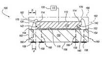
- FIGS. 3-5illustrate aspects of a microelectronic component package 100 in accordance with one embodiment of the invention.
- FIG. 4is a schematic top view of the microelectronic component package 100 .
- FIG. 3is a schematic cross-sectional view of the package 100 taken along line 3 - 3 of FIG. 4 and
- FIG. 5is a side view of the microelectronic component 110 shown in FIGS. 3 and 4 .
- the microelectronic component package 100includes a microelectronic component 110 attached to a mounting surface 152 of a substrate 150 by a cementitious material 140 .
- Aspects of the substrate 150may be similar to aspects of the substrate 50 illustrated in FIGS. 1 and 2 .
- the substrate 150 of the microelectronic component package 100may include a plurality of substrate contacts 154 carried on the mounting surface 152 and a plurality of back contacts 158 carried on a back surface 156 .
- the substrate contacts 154may be electrically coupled to the back contacts 158 by circuitry 160 , e.g., vias through the thickness of the substrate 150 .
- the substrate 150may be flexible or rigid and have any desired configuration.
- the substrate 150may be formed of materials commonly used in microelectronic substrates, such as ceramic, silicon, glass, or combinations thereof.
- the substrate 150may be formed of an organic material or other material suitable for printed circuit boards (PCBs).
- the substrate 150comprises a printed circuitboard such as an FR-4 or FR-5 PCB. If so desired, thermal vias (not shown) may pass through the substrate 150 to assist in cooling the microelectronic component 110 during operation.
- the term “microelectronic component”is intended to cover a variety of different articles.
- the microelectronic component 110may include an integrated circuit 135 (shown schematically in FIGS. 3 and 5 ).
- the microelectronic component 110may comprise a semiconductor die such as a silicon die carrying the integrated circuitry 135 .
- the microelectronic component 110is illustrated in the drawings as comprising a single element, it should be understood that the microelectronic component 110 can comprise any number of subcomponents.
- the microelectronic component 110may comprise two or more stacked semiconductor dies.
- the microelectronic component 110 shown in FIGS. 3-5includes an active surface 112 that carries a plurality of component contacts 114 .
- a back surface 116 of the microelectronic component 110is spaced from, and may be generally parallel to, the active surface 112 . This defines a thickness T ( FIG. 5 ) of the microelectronic component 110 .
- a periphery 120 of the microelectronic component 110extends between the active surface 112 and the back surface 116 .
- the conventional semiconductor die 20 shown in FIGS. 1 and 2has a generally flat edge that extends generally perpendicularly from one surface to the other surface of the die 20 .
- the microelectronic component 110 of FIGS. 3-5includes an irregular or stepped periphery 120 . As shown in FIG. 5 , this stepped periphery includes a first portion 122 that extends rearwardly from the active surface 112 , a third portion 126 that extends inwardly from the back surface 116 , and an intermediate second portion 124 that extends between the first portion 122 and the third portion 126 .
- At least one of the first, second, and third portions 122 , 124 , and 126is oriented at an angle with respect to the active surface 112 that differs from the angle at which at least one of the other portions of the periphery 120 is oriented with respect to the active surface 112 .
- the first and second portions 122 and 126 of the microelectronic component 100 shown in FIGS. 3-5are generally parallel to one another and oriented at an angle that is generally perpendicular to the active surface 112 .
- the second portion 124may be generally parallel to or oriented at an oblique angle, e.g., an acute angle, with respect to the active surface 112 .
- an oblique anglee.g., an acute angle
- the second portion 124is generally parallel to the active surface 112 and meets each of the first and third portions 122 and 126 of the periphery 120 at a right angle. This defines an overhang 125 that extends laterally outwardly beyond a perimeter of the back surface 116 at a location spaced from the back surface 116 .
- the periphery 120 of the microelectronic component 110may have a generally L-shaped notch having a width W defined by the width of the second portion 124 and a height h defined by the third portion 126 .
- Suitable dimensions for the width W and the height hmay vary depending on the size and type of microelectronic component 110 being used, the nature (e.g., initial rheology) of the cementitious material 140 , and the application for which the microelectronic component package 110 is intended.
- the width Wis between about 1 and about 10 mils (about 25-250 microns), with a range of about 2-5 mils (about 50-125 microns) being suitable for many applications.
- the height h of the L-shaped notch in this embodimentmay also range from about 1 mil to about 10 mils (about 25-250 microns). The height h should be sufficient to insure that the active region 113 of the microelectronic component 110 , which may carry some or all of the integrated circuit 135 , remains intact.
- the overhanghas a thickness that includes both the active region 113 and a thickness of the underlying semiconductor body to help preserve the integrity of the active region 113 .
- the height h of the third portion 126 of the periphery 120is no more than about one half of the thickness T of the microelectronic component 110 .
- a height h of about 2-5 mils (about 50-125 microns)is expected to suffice for semiconductor dies that are about 8-10 mils (about 200-250 microns) thick.
- the periphery 120 of the microelectronic component 110extends laterally inwardly in a direction from the active surface 112 to the back surface 116 of the microelectronic component 110 .
- the back surface 116has a surface area that is smaller than the surface area of the active surface 112 of the microelectronic component 110 .
- the profile of the back surface 116(shown in dashed lines in FIG. 4 ) is smaller than the profile of the active surface 112 .
- a transverse width of the active surface 112is greater than the corresponding transverse width of the back surface 116 . If the overhang 125 ( FIG. 5 ) is about 2-6 mils wide, as noted above, the difference in transverse width of the active and back surfaces 112 and 116 would be about 4-12 mils (about 100-300 microns).
- the microelectronic component 110 of FIGS. 3-5is generally rectangular in shape and has a periphery 120 that extends laterally inwardly along each of its four edges. If so desired, the width W of the overhang 125 ( FIG. 5 ) may be substantially constant, generally centering the back surface 116 with respect to the active surface 112 . In other embodiments, the width W of the overhang 125 may vary around the length of the periphery 120 . In an alternative embodiment, only a portion of the periphery 120 of the microelectronic component 110 includes an overhang.
- microelectronic components 110may include one or two rows of component contacts 114 that extend parallel to opposed edges of the microelectronic component 110 rather than extending around the entire periphery of the microelectronic component 110 , as shown in FIG. 4 .
- itmay suffice to include an overhang 125 on one or each of the opposed edges parallel to the row or rows of contacts 114 .
- the remaining edges of the microelectronic component 110may be substantially flat between the active surface 112 and the back surface 116 .
- Other configurations suitable for other specific applicationswill be readily apparent to those of ordinary skill in the art.
- the microelectronic component 110is attached to the substrate 150 with the back surface 116 of the microelectronic component 110 juxtaposed with the mounting surface 152 of the substrate 150 and the active surface 112 of the microelectronic component 110 oriented away from the substrate 150 .
- the second portion ( 124 in FIG. 5 ) of the microelectronic component periphery 120is oriented generally parallel to and spaced from the mounting surface 152 of the substrate 150 . This defines an overhang space 142 between the overhang 125 of the microelectronic component 110 and the mounting surface 152 of the substrate 150 .
- the microelectronic component 110is attached to the substrate 150 by a cementitious material 140 .
- the cementitious material 140bonds at least the back surface 116 of the microelectronic component 110 to the mounting surface 152 of the substrate 150 . As shown in FIG. 3 , it may also adhere to the third portion 126 of the component periphery 120 .
- the cementitious material 140is in direct contact with the back surface 116 of the microelectronic component 110 and the mounting surface 152 of the substrate 150 with no additional intervening layers.
- a layer of a soldermaskmay be disposed between the cementitious material 140 and one or both of the back surface 116 and the mounting surface 152 .
- the cementitious material 140will be flowable or plastically deformable in at least an initial state. In some embodiments, the cementitious material 140 may also be curable into a more rigid state, which may also promote more effective bonding of the microelectronic component 110 to the substrate 150 .
- the cementitious material 140may be an epoxy, a thermoplastic material, a thermoset material, or any other material having suitable chemical and mechanical properties that will adequately bond the microelectronic component 110 to the substrate 150 .
- the cementitious material 140may comprise any one of a variety of commercially available die attach pastes.
- a quantity of the cementitious material 140may be deposited on one or both of the back surface 116 of the microelectronic component 110 and the mounting surface 152 of the substrate 150 .
- the back surface 116 of the microelectronic component 110may then be juxtaposed with a target area associated with the substrate contacts 154 .
- a distance between the back surface 116 and mounting surface 152may be reduced by moving one or more of the substrate 150 and the microelectronic component 110 . As this distance is reduced, any excess cementitious material 140 may squeeze or “bleed” out to define a bead about at least a portion of the perimeter of the back surface 116 .
- the excess cementitious material 140is received in the overhang space 142 between the second portion ( 124 in FIG. 5 ) of the microelectronic component periphery 120 and the mounting surface 152 .
- the excess cementitious material 140may extend into, but not laterally beyond, the overhang space 142 .
- the cementitious material 140may have a profile that is smaller than the profile of the active surface 112 of the microelectronic component 110 but is larger than the profile of the microelectronic component back surface 116 .
- the cementitious material 140extends outwardly beyond the perimeter of the back surface 116 , but covers a surface area of the mounting surface 152 of the substrate 150 that is no greater than the surface area of the active surface 112 of the microelectronic component 110 .
- the wire bond pads 54 of the conventional package 10 of FIG. 1must be spaced a distance d that is sufficient to accommodate any bleed out of the die attach paste 40 without compromising the surface of the bond pads 54 .
- the periphery 62 of the substrate(and, in FIG. 1 , the periphery 82 of the encapsulant 180 ) must be spaced a minimum distance D from the die periphery 28 that is typically at least about 0.8 mm, with most packages 10 having a minimum distance of at least about 1 mm.
- the overhang space 142may accommodate some or all of any cementitious material 140 bleed out, allowing the substrate contacts 154 to be spaced a smaller distance d from the periphery 120 of the microelectronic component 110 .
- Thispermits the use of a smaller substrate 150 having a periphery 162 spaced a smaller minimum distance D that may be less than 1 mm.
- the distance Dmay be on the order of about 0.5 mm or less.
- a distance D of 0.5 mm or less in accordance with embodiments of the inventioncan reduce the overall lateral dimension of the microelectronic component package 100 by 1 mm or more. Particularly for small hand-held devices, e.g., mobile phones, such a reduction in package size can provide substantial benefit.
- a larger diemay be used in a package 100 that is the same size as the conventional package 10 . This may permit more circuitry to be included in the integrated circuit 135 , enhancing performance and circuit design options.
- At least one of the component contacts 114may be electrically coupled to one of the substrate contacts 154 by a bonding wire 170 , typically after the microelectronic component 110 is attached to the substrate 150 by the cementitious material 140 .
- each of the component contacts 114is coupled to a separate one of the substrate contacts 154 by a separate bonding wire 170 .
- the microelectronic component package 100may also include an encapsulant 180 that covers the active surface 112 and at least a portion of the periphery 120 of the microelectronic component 110 ; a portion of the substrate mounting surface 152 ; and the bonding wire or wires 170 .
- the encapsulant 180substantially fills any portion of the overhang space 142 that is not occupied by the bead of cementitious material 140 .
- the encapsulant 180is substantially coextensive with the mounting surface 152 of the substrate 150 , providing an encapsulant periphery 182 that is substantially flush with the periphery 162 of the substrate 150 .
- the encapsulant 180may be delivered as a flowable material into a conventional mold and subsequently cured, e.g., by heat treatment, UV exposure or any combination of heating and UV exposure.
- the cementitious material 140 and the encapsulant 180may both be cured using the same general process, e.g., they may both be UV-curable resins.
- suitable epoxy resins and other dielectric flowable materialsare widely commercially available.
- Embodiments of the present inventionmay provide additional advantages not realized in Tian et al., though. Interposing a spacer between the die and the substrate assembly of this reference elevates the die a distance above the substrate assembly. This, in turn, raises the front surface of the die.
- the microelectronic component 110which may comprise a semiconductor die, is separated from the mounting surface 152 of the substrate 150 only by a relatively thin layer of cementitious material 140 . As a consequence, the additional height of a separate support is eliminated, allowing a reduced thickness between the active surface 112 of the microelectronic component 110 and the mounting surface 52 of the substrate 150 .
- this reduced thickness in the package 100 of FIG. 3permits the outer surface of the encapsulant 180 to be closer to the substrate 150 , reducing the thickness and weight of the package 100 .
- an encapsulant having the same thickness as that employed in Tian et al.is employed in the package 100 of FIG. 3 , there will be more clearance between the outer surface of the encapsulant 180 and the loop height of the bonding wires 170 . This increased clearance reduces the chance that a portion of the bonding wire may be exposed and subjected to environmental degradation, and may also decrease the risk of undue wire sweep during the encapsulant molding process.
- the bonding wires 170 in FIG. 3may be shorter than those employed by Tian et al. because they traverse a shorter distance between the contacts 114 and 154 . Shorter wires 170 , in turn, can improve electrical performance and reduce costs.
- FIGS. 6-8illustrate various microelectronic components in accordance with other embodiments of the invention. Each of these microelectronic components may be employed in a microelectronic component package in accordance with the invention, e.g., by using the microelectronic component of any one of FIG. 6-8 in place of the microelectronic component 110 in FIGS. 3 and 4 .
- the microelectronic component 210has an active surface 212 spaced from a back surface 216 by a thickness T.
- a plurality of component contacts 214may be carried by the active surface 212 and electrically coupled to an integrated circuit 235 carried at least in part in an active region 213 of the microelectronic component 210 .
- the periphery of the microelectronic component 210has a first portion 222 oriented at a first angle with respect to the active surface 212 and a second surface 224 oriented at a second, different angle with respect to the active surface 212 . In the particular implementation shown in FIG.
- the first portion 222may be generally perpendicular to the active surface 212 and the second portion 224 extends laterally inwardly in a direction from the active surface 212 toward the back surface 216 .
- the junction 223 between the first portion 222 and the second portion 224may be spaced a height h inwardly from the plane of the back surface 216 and spaced a width W laterally outwardly from a perimeter of the back surface 216 .
- the thickness T, height h, and width W measurementsmay be similar to those outlined above for the microelectronic component 110 ( FIG. 5 ).
- the first portion 222occupies a remaining portion R of the thickness T of the microelectronic component 210 .
- this remainder Rincludes both the active region 213 and a portion of the underlying base.
- this microelectronic component 210is juxtaposed with a substrate 150 ( FIGS. 3 and 4 ) in forming a microelectronic component package similar to the package 100 discussed above, the juxtaposition of the second portion 224 of the component periphery 220 with the mounting surface of the substrate will define an overhang space analogous to the overhang space 142 shown in FIG. 3 .
- FIG. 7illustrates a microelectronic component 310 in accordance with another embodiment of the invention.
- This microelectronic component 310includes an active surface 312 spaced from a back surface 316 by a thickness T.
- Component contacts 314 carried by the active surface 312may be in electrical communication with an integrated circuit 335 carried at least in part in an active region 313 of the microelectronic component 310 .
- the periphery 320may be generally flat along each side of the microelectronic component 310 , but oriented obliquely to, e.g., at an acute angle with respect to, the active surface 312 .
- the perimeter of the back surface 316may be spaced laterally inwardly a width W from the perimeter of the active surface 312 .
- the width Wmay be similar to, or perhaps less than, those discussed above in connection with the microelectronic component 110 of FIG. 5 .
- This microelectronic component 310will also define a space between the periphery 320 and the mounting surface of a substrate analogous to the overhang space 142 shown in FIG. 3 .
- FIG. 8A microelectronic component 410 in accordance with still another embodiment of the invention is shown in FIG. 8 .
- This microelectronic component 410includes an active surface 412 spaced from a back surface 416 by a thickness T.
- Component contacts 414 carried by the active surface 412may be in electrical communication within an integrated circuit 435 carried at least in part in an active region 413 of the microelectronic component 410 .
- the periphery 420 of the microelectronic component 410includes a first portion 422 and a second portion 424 . Unlike the preceding embodiments, the second portion 424 has a generally arcuate shape.
- a perimeter of the back surface 416is spaced a width W laterally inwardly from the perimeter of the active surface 412 .
- the second portion 424 of the perimeter 420meets the first portion 422 at a height h inwardly from the back surface 416 , leaving an overhang 425 spaced from the point of the back surface 416 .
- the height his more than fifty percent of the thickness T, but the overhang 425 still includes the active region 413 and a portion of the underlying base to better insure the integrity of the active region 413 .
- the height h of the first portion 422 from the back surface 416may be on the order of no greater than fifty percent of the thickness T.
- FIGS. 9-11schematically illustrate a microfeature workpiece, typified as a semiconductor wafer 500 , that may be processed in accordance with an embodiment of the invention.
- the wafer 500has a front surface 512 and a back surface 516 ( FIG. 11 ) spaced from the front surface 512 by a wafer thickness T.
- the wafer 500may include a plurality of microelectronic components 520 , e.g., semiconductor dies, typically arranged in a regular array.
- the aligned spaces between the microelectronic components 520may define a set of generally parallel first “streets” 522 ( FIG. 10 ) and a set of generally parallel second streets 524 ( FIG. 10 ).
- the first streets 522may be oriented at an angle, e.g., 90 degrees, with respect to the second streets 524 .
- each of the microelectronic components 520may include a plurality of contacts 525 carried by the front surface 512 ( FIG. 9 ) of the wafer 500 .
- a set of these contacts 525may be associated with each of the microelectronic components 520 . (The contacts 525 have been omitted from FIGS. 9 and 11 - 14 to simplify the illustration.)
- FIGS. 11-14schematically illustrate stages in the manufacture of a microelectronic component 110 in accordance with one particular embodiment of the invention.
- the wafer 500is attached to a first temporary support 560 , e.g., a polymeric film such as a die attach tape.
- the terminal-bearing front surface 512 of the wafer 500is juxtaposed with, and may be adhered directly to, the temporary support 560 .
- the back surface 516 of the wafer 500is oriented away from the temporary support 560 .
- a series of generally parallel channels 530may extend inwardly from the back surface 516 of the wafer 500 toward the front surface 512 .
- the depth of these channels 530may be substantially equivalent to the height h of the third segment 126 of the microelectronic component periphery 120 shown in FIG. 5 , e.g., about 2-5 mils (about 50-125 microns).
- the wafer 500may be processed in accordance with embodiments of the invention before the back surface 516 of the wafer 500 is planarized to define a final target thickness of the wafer 500 and, hence, of the microelectronic components 520 .
- the depth of the channels 530may include the desired height h and the additional thickness of the wafer 500 to be removed in the planarizing process.
- the channel 530may extend a distance of at least about 1 mil (about 25 microns) into the target thickness, i.e., at least about 1 mil beyond the thickness to be removed by planarizing.
- the channel 530may extend into the target thickness about 1 mil to about one-half the target thickness.
- the channels 530also have a channel width C that is at least as great as the width W of the second portion 124 of the microelectronic component periphery 120 shown in FIG. 5 . In the particular embodiment shown in FIGS. 12-14 , this channel width C is greater than twice the target width W.
- the channels 530may follow a path that generally corresponds to the path of the streets 522 between adjacent microelectronic components 520 .
- a midline of each of the channels 530may be generally parallel to and follow along a midline of one of the streets 522 .
- the midlines of the channels 530may be spaced laterally from the midlines of the associated streets 522 . Such an embodiment may be advantageous where an overhang 125 ( FIG. 5 ) is provided only along one edge of the microelectronic component 520 , for example.
- FIG. 12illustrates a single pair of parallel channels 530 , each of which follows a path that corresponds to one of the generally parallel first streets 522 .
- a similar series of parallel channels 530may follow paths that correspond to the set of second streets 524 ( FIG. 10 ).
- the resultant second set of parallel channels(not shown in FIG. 12 ) would intersect at least some of the channels 530 that follow paths correlated to the first streets 522 .
- the channels 530may be formed using any of a variety of techniques known for cutting wafers 500 .
- the channels 530may be formed using a conventional wafer saw, with the dicing blade width of the wafer saw being generally commensurate with the channel width C.
- Another embodiment of the inventionmay employ laser ablation or selective etching to form the channels 530 .
- the temporary support 560 shown in FIGS. 11 and 12may serve multiple functions.
- the temporary support 560may physically support the wafer 500 during the process of cutting the channels 530 .
- the temporary support 560may also or may instead protect the contact-bearing front surface 512 of the wafer 500 during the process of forming the channels 530 . Both of these functions may also be useful in a planarizing step if the channels 530 are formed in the wafer 500 before the wafer 500 has been planarized to the target thickness T. If the functions of the temporary support 560 are deemed unnecessary, the temporary support 560 may be omitted and the channels 530 may be formed without employing the temporary support 560 .
- the temporary support 560has been removed from the front surface 512 of the wafer 500 .
- a second temporary support 562has been attached to the back surface 516 of the wafer 500 .
- Suitable materials for the temporary support 562may be substantially the same as those mentioned above for the first temporary support 560 .
- the temporary support 562may be attached to the generally coplanar portions of the back surface 516 left after forming the channels 530 . This will leave a remaining thickness r of the wafer 500 spaced above the temporary support 562 .
- the wafer 500may be separated or “singulated” into a series of separate microelectronic components, each of which may be the same as the microelectronic component 110 of FIGS. 3-5 . In the embodiment shown in FIG. 14 , this is accomplished by forming a series of parallel gaps 540 that extend entirely through the remaining thickness r so the gaps 540 communicate with the associated channels 530 . In other embodiments, the gaps 540 may not extend completely through the remaining thickness r, leaving a relatively thin connection (not shown) between adjacent microelectronic components 520 . As is known in the art, the wafer 500 may be broken along these thin sections, with the combination of the gaps 540 and channels 530 serving as score lines between adjacent microelectronic components 520 .
- the gaps 540 in FIG. 14generally follow along the streets 522 in the wafer 500 of FIG. 13 . As the embodiment of FIGS. 12 and 13 generally aligns the midlines of the channels 530 with the midline of the associated streets 522 , this will generally center the gap 540 with respect to the associated channel 530 . In other embodiments, the gap 540 may be displaced laterally from the position shown in FIG. 14 , e.g., at one side or the other of the associated channel 530 .
- the channel width C of the channels 530may be greater than a gap width G of the associated gaps 540 .
- the relative difference in the dimensions of the channels 530 and the associated gaps 540will depend at least in part on the desired width W of the overhang 125 in the finished microelectronic component 110 . If the microelectronic component 110 includes an overhang 125 on only one of its two opposed sides, the channel width C may be approximately equal to the sum of the desired overhang width W and the gap width G.
- the gap 540may then be cut into or through the remaining thickness r ( FIG. 13 ) with a side of the gap 540 generally aligned with a side of the associated channel 530 .
- the microelectronic component 110has an overhang 125 on each of the two opposed sides shown in the drawing. Each of these overhangs 125 may have substantially the same overhang width W.
- the channel width C in this embodimentmay be approximately equal to the gap width G plus two times the overhang width W.
- the channel width Cshould be about 4-12 mils (about 100-300 microns) greater than the gap width G.
- the gaps 540may be formed using a wafer saw having a blade width of about 1.2-4 mils (about 30-100 microns).
- the channel width Cwould be about 5.2-16 mils (about 130-400 microns).
- These channels 530may be formed using a wafer saw with a dicing blade width approximately equal to the channel width C.
- FIGS. 11-14illustrate one possible process for forming microelectronic components, e.g., microelectronic components 110 , in accordance with one embodiment of the invention.
- the first temporary support 560may remain attached to the front surface 512 of the wafer 500 when forming the gaps 540 and a dicing blade of a wafer saw or other cutting tool may be directed into the channels 530 to cut the gaps 540 from the channel 530 toward the front surface 512 .
- the gap 540may extend through some or all of the remaining thickness r; if the gaps 540 do not extend through the entire remaining thickness r, they may serve as score lines for breaking the wafer 500 in a subsequent step.
- the wafer 500may be diced by forming the gap 540 through some or substantially all of the thickness T of the wafer 500 .
- the channels 530may then be formed by cutting inwardly from the back surface 516 of the wafer 500 , effectively widening a portion of the gap 540 to form a kerf on one or both of the adjacent edges of the microelectronic components 110 .
- the overhangs 125may be formed on already singulated microelectronic components 110 by cutting one kerf along one edge of the microelectronic component 110 and cutting another kerf along the opposite edge of the microelectronic component 110 .
Landscapes
- Engineering & Computer Science (AREA)
- Computer Hardware Design (AREA)
- Microelectronics & Electronic Packaging (AREA)
- Power Engineering (AREA)
- Die Bonding (AREA)
- Manufacturing Of Printed Wiring (AREA)
- Structures Or Materials For Encapsulating Or Coating Semiconductor Devices Or Solid State Devices (AREA)
Abstract
Description
- This application claims foreign priority benefits of Singapore Application No. 200306527-3, filed Oct. 31, 2003, the entirety of which is incorporated herein by reference.
- 1. Technical Field
- The present invention generally relates to microelectronic components.
- Aspects of the invention have particular utility in connection with packaged microelectronic components, e.g., packaged semiconductor dies.
- 2. Background
FIGS. 1 and 2 schematically illustrate a conventional diepackage 10.- This
package 10 includes asemiconductor die 20 that is attached to afront surface 52 of asubstrate 50 by a dieattach paste 40. The dieattach paste 40 is typically applied in a plastic or flowable state and the die20 is pressed onto the paste, causingexcess paste 40 to bleed out from underneath the die20. A plurality ofbonding wires 70 electrically connectcontacts 24 carried by the die20 tobond pads 54 carried by theupper surface 52 of thesubstrate 50. Thebond pads 54 of thesubstrate 50 are connected toball bond pads 58 on theback surface 56 of thesubstrate 50 byvias 60. Theseball bond pads 58 may be used, for example, to carry solder balls to electrically connect thepackage 10 to another microelectronic component. An encapsulant80 (shown in phantom andFIG. 1 ) covers the top andsides 28 of the die20. - Generally, the
bond pads 54 of thesubstrate 50 must be spaced a sufficient distance d to minimize the chance that thedie attach paste 40 will bleed out far enough to cover the bond-pad 54. To accommodate the size of thebond pads 54, theperiphery 62 of thesubstrate 50 is spaced at least a minimum distance D from theperiphery 28 of thedie 20. As suggested inFIG. 1 , the lateral dimensions of theencapsulant 80 are typically about the same as those of thesubstrate 50, such that theperiphery 82 of theencapsulant 80 is generally flush with theperiphery 62 of thesubstrate 50. Typical dimensions for the minimum distance D are at least about one millimeter. At least oneconventional package 10 achieves a minimum distance D of about 0.8 millimeters by dicing the packages with the saw blade cutting the width of thebond pads 54. Since theperiphery 62 is spaced the minimum distance D from each side of therectangular die 20, such aconventional package 10 is about 1.6 millimeters wider than the die20 of thepackage 10. - Market pressures to reduce the size of electronic devices, e.g., mobile telephones and hand-held computing devices, place a premium on the space or “real estate” available for mounting microelectronic components on a printed circuitboard or the like. Similar density pressures also impact manufacturers of computers and other larger-scale electronic devices. An extra 2.5 millimeters per
package 10, for example, can significantly add to the dimensions of an array of packaged memory chips, for example. FIG. 1 is a schematic cross-sectional view of a conventional die package taken along line1-1 ofFIG. 2 .FIG. 2 is a schematic top view of the conventional die package ofFIG. 1 .FIG. 3 is a schematic cross-sectional view of a microelectronic component package in accordance with one embodiment of the invention, taken along line3-3 ofFIG. 4 .FIG. 4 is a schematic top view of the microelectronic component package ofFIG. 3 .FIG. 5 is an enlarged, schematic side view of the microelectronic component of the microelectronic component package ofFIGS. 3 and 4 .FIG. 6 is a schematic side view of a microelectronic component in accordance with another embodiment of the invention.FIG. 7 is a schematic side view of a different embodiment of the invention.FIG. 8 is a schematic side view of a microelectronic component in accordance with still another embodiment of the invention.FIG. 9 is a schematic top view of a semiconductor wafer that may be processed in accordance with other embodiments of the invention.FIG. 10 is an enlarged view of the encircled portion ofFIG. 9 designated “FIG. 10 .”FIGS. 11-14 schematically illustrate sequential stages of processing the semiconductor wafer ofFIGS. 9 and 10 in accordance with one particular embodiment of the invention.- A. Overview
- Various embodiments of the present invention provide packaged microelectronic components and methods of manufacturing packaged microelectronic components. The terms “microelectronic component” and “microelectronic component assembly” may encompass a variety of articles of manufacture, including one or more memory modules (e.g., SIMM, DIMM, DRAM, flash-memory), ASICs, processors, semiconductor wafers, semiconductor dies singulated from such wafers, or any of a variety of other types of microelectronic devices or components therefor.
- A microelectronic component package in accordance with one embodiment of the invention includes a substrate, a microelectronic component, and a cementitious material. The substrate has a mounting surface. The microelectronic component has a first surface and a second surface. The first surface has a surface area greater than a surface area of the second surface. The cementitious material attaches the second surface of the microelectronic component to the mounting surface of the substrate. The cementitious material extends outwardly beyond a perimeter of the second surface of the microelectronic component, but covers a surface area of the mounting surface that is no greater than the surface area of the first surface of the microelectronic component.
- Another embodiment of the invention provides a microelectronic component package that also includes a substrate, a microelectronic component, and a cementitious material. The microelectronic component in this embodiment has a first side having a first profile and a second side having a second profile that is smaller than the first profile. A difference between the first profile and the second profile defines a lateral overhang. The cementitious material attaches the second side of the microelectronic component to the substrate. A quantity of the cementitious material extends into, but not laterally beyond, an overhang space between the overhang and the substrate.
- A microelectronic component package in accordance with a further embodiment of the invention includes a substrate, a microelectronic component that has a front dimension larger than a back dimension, and a paste between the microelectronic component and the substrate that bonds the microelectronic component to the substrate. The paste has a dimension that is larger than the back dimension, but is smaller than the front dimension.
- A microelectronic component package in accordance with still another embodiment of the invention includes a substrate, a semiconductor die, at least one wire, and an encapsulant. The semiconductor die has a first surface, a second surface, and an edge extending between the first surface and the second surface. The first surface has a first surface area and the second surface has a second surface area that is less than the first surface area. The at least one wire electrically couples a component contact carried by the first surface to a contact carried by the substrate. The encapsulant covers the semiconductor die and the at least one wire. The encapsulant has an edge spaced laterally from the edge of the semiconductor die by no more than about 0.5 millimeters.
- A microfeature workpiece in accordance with an alternative embodiment of the invention comprises a wafer that has a first surface and a second surface and includes first and second microelectronic components. The first surface carries a first set of contacts associated with the first microelectronic component and a second set of contacts associated with the second microelectronic component. The second surface is spaced from the first surface by a wafer thickness. A gap extends along a first path between the first set of contacts and the second set of contacts. The gap extends inwardly from the first surface a first distance that is less than the wafer thickness, defining a remaining distance between the gap and a plane of the second surface. A channel extends inwardly from the second surface a second distance that is less than or equal to the remaining distance. The channel is wider than the gap and follows a second path that corresponds to the first path. If so desired, the second path may be directly juxtaposed with the first path and/or the channel may be in direct communication with the gap.
- One additional embodiment of the invention provides a method of manufacturing a microelectronic component. In accordance with this embodiment, a first kerf is formed in a first surface along a first edge of a microelectronic component. The microelectronic component has a target thickness and the first kerf extends into the target thickness a first distance of between about one mil and about one-half the target thickness. A second kerf is formed in the first surface along a second edge of the microelectronic component. The second kerf extends into the target thickness a second distance of between about one mil and about one-half the target thickness. The first surface of the microelectronic component is attached to a surface of a substrate.
- For ease of understanding, the following discussion is broken down into two areas of emphasis. The first section describes aspects of microelectronic components in certain embodiments of the invention. The second section outlines methods of manufacturing microelectronic components in accordance with other embodiments of the invention.
- B. Packaged Microelectronic Components
FIGS. 3-5 illustrate aspects of amicroelectronic component package 100 in accordance with one embodiment of the invention.FIG. 4 is a schematic top view of themicroelectronic component package 100.FIG. 3 is a schematic cross-sectional view of thepackage 100 taken along line3-3 ofFIG. 4 andFIG. 5 is a side view of themicroelectronic component 110 shown inFIGS. 3 and 4 .- Turning first to
FIGS. 3 and 4 , themicroelectronic component package 100 includes amicroelectronic component 110 attached to a mountingsurface 152 of asubstrate 150 by acementitious material 140. Aspects of thesubstrate 150 may be similar to aspects of thesubstrate 50 illustrated inFIGS. 1 and 2 . In particular, thesubstrate 150 of themicroelectronic component package 100 may include a plurality ofsubstrate contacts 154 carried on the mountingsurface 152 and a plurality ofback contacts 158 carried on aback surface 156. Thesubstrate contacts 154 may be electrically coupled to theback contacts 158 bycircuitry 160, e.g., vias through the thickness of thesubstrate 150. - The
substrate 150 may be flexible or rigid and have any desired configuration. In one embodiment, thesubstrate 150 may be formed of materials commonly used in microelectronic substrates, such as ceramic, silicon, glass, or combinations thereof. Alternatively, thesubstrate 150 may be formed of an organic material or other material suitable for printed circuit boards (PCBs). In one particular embodiment, thesubstrate 150 comprises a printed circuitboard such as an FR-4 or FR-5 PCB. If so desired, thermal vias (not shown) may pass through thesubstrate 150 to assist in cooling themicroelectronic component 110 during operation. - As noted above, the term “microelectronic component” is intended to cover a variety of different articles. In many embodiments, the
microelectronic component 110 may include an integrated circuit135 (shown schematically inFIGS. 3 and 5 ). For example, themicroelectronic component 110 may comprise a semiconductor die such as a silicon die carrying theintegrated circuitry 135. Although themicroelectronic component 110 is illustrated in the drawings as comprising a single element, it should be understood that themicroelectronic component 110 can comprise any number of subcomponents. For example, themicroelectronic component 110 may comprise two or more stacked semiconductor dies. - The
microelectronic component 110 shown inFIGS. 3-5 includes anactive surface 112 that carries a plurality ofcomponent contacts 114. Aback surface 116 of themicroelectronic component 110 is spaced from, and may be generally parallel to, theactive surface 112. This defines a thickness T (FIG. 5 ) of themicroelectronic component 110. Aperiphery 120 of themicroelectronic component 110 extends between theactive surface 112 and theback surface 116. - The conventional semiconductor die20 shown in
FIGS. 1 and 2 has a generally flat edge that extends generally perpendicularly from one surface to the other surface of thedie 20. In contrast, themicroelectronic component 110 ofFIGS. 3-5 includes an irregular or steppedperiphery 120. As shown inFIG. 5 , this stepped periphery includes afirst portion 122 that extends rearwardly from theactive surface 112, athird portion 126 that extends inwardly from theback surface 116, and an intermediatesecond portion 124 that extends between thefirst portion 122 and thethird portion 126. In one embodiment of the invention, at least one of the first, second, andthird portions active surface 112 that differs from the angle at which at least one of the other portions of theperiphery 120 is oriented with respect to theactive surface 112. The first andsecond portions microelectronic component 100 shown inFIGS. 3-5 are generally parallel to one another and oriented at an angle that is generally perpendicular to theactive surface 112. Thesecond portion 124 may be generally parallel to or oriented at an oblique angle, e.g., an acute angle, with respect to theactive surface 112. In the particular embodiment shown inFIG. 5 , thesecond portion 124 is generally parallel to theactive surface 112 and meets each of the first andthird portions periphery 120 at a right angle. This defines anoverhang 125 that extends laterally outwardly beyond a perimeter of theback surface 116 at a location spaced from theback surface 116. - As suggested in
FIG. 5 , theperiphery 120 of themicroelectronic component 110 may have a generally L-shaped notch having a width W defined by the width of thesecond portion 124 and a height h defined by thethird portion 126. Suitable dimensions for the width W and the height h may vary depending on the size and type ofmicroelectronic component 110 being used, the nature (e.g., initial rheology) of thecementitious material 140, and the application for which themicroelectronic component package 110 is intended. In one embodiment of the invention employing a semiconductor die as themicroelectronic component 100, the width W is between about 1 and about 10 mils (about 25-250 microns), with a range of about 2-5 mils (about 50-125 microns) being suitable for many applications. The height h of the L-shaped notch in this embodiment may also range from about 1 mil to about 10 mils (about 25-250 microns). The height h should be sufficient to insure that theactive region 113 of themicroelectronic component 110, which may carry some or all of theintegrated circuit 135, remains intact. In the embodiment shown, the overhang has a thickness that includes both theactive region 113 and a thickness of the underlying semiconductor body to help preserve the integrity of theactive region 113. In one particular-embodiment, the height h of thethird portion 126 of theperiphery 120 is no more than about one half of the thickness T of themicroelectronic component 110. For example, a height h of about 2-5 mils (about 50-125 microns) is expected to suffice for semiconductor dies that are about 8-10 mils (about 200-250 microns) thick. - By virtue of its laterally inwardly extending
second portion 124, theperiphery 120 of themicroelectronic component 110 extends laterally inwardly in a direction from theactive surface 112 to theback surface 116 of themicroelectronic component 110. As a consequence, theback surface 116 has a surface area that is smaller than the surface area of theactive surface 112 of themicroelectronic component 110. The profile of the back surface116 (shown in dashed lines inFIG. 4 ) is smaller than the profile of theactive surface 112. In this illustrated embodiment, a transverse width of theactive surface 112 is greater than the corresponding transverse width of theback surface 116. If the overhang125 (FIG. 5 ) is about 2-6 mils wide, as noted above, the difference in transverse width of the active andback surfaces - The
microelectronic component 110 ofFIGS. 3-5 is generally rectangular in shape and has aperiphery 120 that extends laterally inwardly along each of its four edges. If so desired, the width W of the overhang125 (FIG. 5 ) may be substantially constant, generally centering theback surface 116 with respect to theactive surface 112. In other embodiments, the width W of theoverhang 125 may vary around the length of theperiphery 120. In an alternative embodiment, only a portion of theperiphery 120 of themicroelectronic component 110 includes an overhang. Somemicroelectronic components 110, for example, may include one or two rows ofcomponent contacts 114 that extend parallel to opposed edges of themicroelectronic component 110 rather than extending around the entire periphery of themicroelectronic component 110, as shown inFIG. 4 . For such amicroelectronic component 110, it may suffice to include anoverhang 125 on one or each of the opposed edges parallel to the row or rows ofcontacts 114. The remaining edges of themicroelectronic component 110 may be substantially flat between theactive surface 112 and theback surface 116. Other configurations suitable for other specific applications will be readily apparent to those of ordinary skill in the art. - As shown in
FIG. 3 , themicroelectronic component 110 is attached to thesubstrate 150 with theback surface 116 of themicroelectronic component 110 juxtaposed with the mountingsurface 152 of thesubstrate 150 and theactive surface 112 of themicroelectronic component 110 oriented away from thesubstrate 150. In this orientation, the second portion (124 inFIG. 5 ) of themicroelectronic component periphery 120 is oriented generally parallel to and spaced from the mountingsurface 152 of thesubstrate 150. This defines anoverhang space 142 between theoverhang 125 of themicroelectronic component 110 and the mountingsurface 152 of thesubstrate 150. - As noted above, the
microelectronic component 110 is attached to thesubstrate 150 by acementitious material 140. In particular, thecementitious material 140 bonds at least theback surface 116 of themicroelectronic component 110 to the mountingsurface 152 of thesubstrate 150. As shown inFIG. 3 , it may also adhere to thethird portion 126 of thecomponent periphery 120. In the embodiment illustrated inFIG. 3 , thecementitious material 140 is in direct contact with theback surface 116 of themicroelectronic component 110 and the mountingsurface 152 of thesubstrate 150 with no additional intervening layers. In another embodiment, a layer of a soldermask may be disposed between thecementitious material 140 and one or both of theback surface 116 and the mountingsurface 152. - It is anticipated that the
cementitious material 140 will be flowable or plastically deformable in at least an initial state. In some embodiments, thecementitious material 140 may also be curable into a more rigid state, which may also promote more effective bonding of themicroelectronic component 110 to thesubstrate 150. Thecementitious material 140 may be an epoxy, a thermoplastic material, a thermoset material, or any other material having suitable chemical and mechanical properties that will adequately bond themicroelectronic component 110 to thesubstrate 150. In embodiments employing a semiconductor die as themicroelectronic component 110, for example, thecementitious material 140 may comprise any one of a variety of commercially available die attach pastes. - In assembling the
microelectronic component package 100, a quantity of thecementitious material 140 may be deposited on one or both of theback surface 116 of themicroelectronic component 110 and the mountingsurface 152 of thesubstrate 150. Theback surface 116 of themicroelectronic component 110 may then be juxtaposed with a target area associated with thesubstrate contacts 154. A distance between theback surface 116 and mountingsurface 152 may be reduced by moving one or more of thesubstrate 150 and themicroelectronic component 110. As this distance is reduced, any excesscementitious material 140 may squeeze or “bleed” out to define a bead about at least a portion of the perimeter of theback surface 116. At least some, and preferably at least a majority, of the excesscementitious material 140 is received in theoverhang space 142 between the second portion (124 inFIG. 5 ) of themicroelectronic component periphery 120 and the mountingsurface 152. In one useful embodiment, the excesscementitious material 140 may extend into, but not laterally beyond, theoverhang space 142. - As suggested in
FIG. 4 , thecementitious material 140 may have a profile that is smaller than the profile of theactive surface 112 of themicroelectronic component 110 but is larger than the profile of the microelectronic component backsurface 116. In one embodiment, thecementitious material 140 extends outwardly beyond the perimeter of theback surface 116, but covers a surface area of the mountingsurface 152 of thesubstrate 150 that is no greater than the surface area of theactive surface 112 of themicroelectronic component 110. - Comparing
FIGS. 1 and 3 , highlights certain benefits of embodiments of the present invention. As noted above, thewire bond pads 54 of theconventional package 10 ofFIG. 1 must be spaced a distance d that is sufficient to accommodate any bleed out of the die attachpaste 40 without compromising the surface of thebond pads 54. As a consequence, theperiphery 62 of the substrate (and, inFIG. 1 , theperiphery 82 of the encapsulant180) must be spaced a minimum distance D from thedie periphery 28 that is typically at least about 0.8 mm, withmost packages 10 having a minimum distance of at least about 1 mm. - In contrast, the
overhang space 142 may accommodate some or all of anycementitious material 140 bleed out, allowing thesubstrate contacts 154 to be spaced a smaller distance d from theperiphery 120 of themicroelectronic component 110. This, in turn, permits the use of asmaller substrate 150 having aperiphery 162 spaced a smaller minimum distance D that may be less than 1 mm. - In one advantageous embodiment, the distance D may be on the order of about 0.5 mm or less.
- Compared to a
conventional die package 10 having a minimum distance D of about 1 mm from each side of the die20, employing a distance D of 0.5 mm or less in accordance with embodiments of the invention can reduce the overall lateral dimension of themicroelectronic component package 100 by 1 mm or more. Particularly for small hand-held devices, e.g., mobile phones, such a reduction in package size can provide substantial benefit. Alternatively, a larger die may be used in apackage 100 that is the same size as theconventional package 10. This may permit more circuitry to be included in theintegrated circuit 135, enhancing performance and circuit design options. - At least one of the
component contacts 114 may be electrically coupled to one of thesubstrate contacts 154 by abonding wire 170, typically after themicroelectronic component 110 is attached to thesubstrate 150 by thecementitious material 140. In the particular embodiment shown inFIGS. 3 and 4 , each of thecomponent contacts 114 is coupled to a separate one of thesubstrate contacts 154 by aseparate bonding wire 170. - As suggested by a broken line in
FIG. 3 , themicroelectronic component package 100 may also include anencapsulant 180 that covers theactive surface 112 and at least a portion of theperiphery 120 of themicroelectronic component 110; a portion of thesubstrate mounting surface 152; and the bonding wire orwires 170. In one embodiment, theencapsulant 180 substantially fills any portion of theoverhang space 142 that is not occupied by the bead ofcementitious material 140. In the design shown inFIG. 3 , theencapsulant 180 is substantially coextensive with the mountingsurface 152 of thesubstrate 150, providing anencapsulant periphery 182 that is substantially flush with theperiphery 162 of thesubstrate 150. - Any of a variety of materials may be used as the
encapsulant 180. In one embodiment, theencapsulant 180 may be delivered as a flowable material into a conventional mold and subsequently cured, e.g., by heat treatment, UV exposure or any combination of heating and UV exposure. In one useful implementation, thecementitious material 140 and theencapsulant 180 may both be cured using the same general process, e.g., they may both be UV-curable resins. A wide variety of suitable epoxy resins and other dielectric flowable materials are widely commercially available. - U.S. Patent Application Publication No. US 2003/0107138 A1 (Tian et al., the entirety of which is incorporated herein by reference), which is owned by the assignee of the present invention, discloses a variety of die package designs. In several of those designs, a support is disposed between the die and the surface of a substrate assembly. In at least one of the disclosed designs, the support is smaller than the die. The support is attached to the substrate by a paste, e.g., a flowable die attach paste. The size difference between the support and the die is said to accommodate bleed out of the paste.
- Embodiments of the present invention may provide additional advantages not realized in Tian et al., though. Interposing a spacer between the die and the substrate assembly of this reference elevates the die a distance above the substrate assembly. This, in turn, raises the front surface of the die. In the
package 100 shown inFIG. 3 , themicroelectronic component 110, which may comprise a semiconductor die, is separated from the mountingsurface 152 of thesubstrate 150 only by a relatively thin layer ofcementitious material 140. As a consequence, the additional height of a separate support is eliminated, allowing a reduced thickness between theactive surface 112 of themicroelectronic component 110 and the mountingsurface 52 of thesubstrate 150. - In one implementation, this reduced thickness in the
package 100 ofFIG. 3 permits the outer surface of theencapsulant 180 to be closer to thesubstrate 150, reducing the thickness and weight of thepackage 100. Alternatively, if an encapsulant having the same thickness as that employed in Tian et al. is employed in thepackage 100 ofFIG. 3 , there will be more clearance between the outer surface of theencapsulant 180 and the loop height of thebonding wires 170. This increased clearance reduces the chance that a portion of the bonding wire may be exposed and subjected to environmental degradation, and may also decrease the risk of undue wire sweep during the encapsulant molding process. In addition, thebonding wires 170 inFIG. 3 may be shorter than those employed by Tian et al. because they traverse a shorter distance between thecontacts Shorter wires 170, in turn, can improve electrical performance and reduce costs. FIGS. 6-8 illustrate various microelectronic components in accordance with other embodiments of the invention. Each of these microelectronic components may be employed in a microelectronic component package in accordance with the invention, e.g., by using the microelectronic component of any one ofFIG. 6-8 in place of themicroelectronic component 110 inFIGS. 3 and 4 .- In
FIG. 6 , themicroelectronic component 210 has anactive surface 212 spaced from aback surface 216 by a thickness T. A plurality ofcomponent contacts 214 may be carried by theactive surface 212 and electrically coupled to anintegrated circuit 235 carried at least in part in anactive region 213 of themicroelectronic component 210. The periphery of themicroelectronic component 210 has afirst portion 222 oriented at a first angle with respect to theactive surface 212 and asecond surface 224 oriented at a second, different angle with respect to theactive surface 212. In the particular implementation shown inFIG. 6 , thefirst portion 222 may be generally perpendicular to theactive surface 212 and thesecond portion 224 extends laterally inwardly in a direction from theactive surface 212 toward theback surface 216. Thejunction 223 between thefirst portion 222 and thesecond portion 224 may be spaced a height h inwardly from the plane of theback surface 216 and spaced a width W laterally outwardly from a perimeter of theback surface 216. The thickness T, height h, and width W measurements may be similar to those outlined above for the microelectronic component110 (FIG. 5 ). InFIG. 6 , thefirst portion 222 occupies a remaining portion R of the thickness T of themicroelectronic component 210. In one embodiment, this remainder R includes both theactive region 213 and a portion of the underlying base. When thismicroelectronic component 210 is juxtaposed with a substrate150 (FIGS. 3 and 4 ) in forming a microelectronic component package similar to thepackage 100 discussed above, the juxtaposition of thesecond portion 224 of thecomponent periphery 220 with the mounting surface of the substrate will define an overhang space analogous to theoverhang space 142 shown inFIG. 3 . FIG. 7 illustrates amicroelectronic component 310 in accordance with another embodiment of the invention. Thismicroelectronic component 310 includes anactive surface 312 spaced from aback surface 316 by a thicknessT. Component contacts 314 carried by theactive surface 312 may be in electrical communication with anintegrated circuit 335 carried at least in part in anactive region 313 of themicroelectronic component 310. In the particular illustrated embodiment, theperiphery 320 may be generally flat along each side of themicroelectronic component 310, but oriented obliquely to, e.g., at an acute angle with respect to, theactive surface 312. The perimeter of theback surface 316 may be spaced laterally inwardly a width W from the perimeter of theactive surface 312. In one embodiment, the width W may be similar to, or perhaps less than, those discussed above in connection with themicroelectronic component 110 ofFIG. 5 . Thismicroelectronic component 310 will also define a space between theperiphery 320 and the mounting surface of a substrate analogous to theoverhang space 142 shown inFIG. 3 .- A
microelectronic component 410 in accordance with still another embodiment of the invention is shown inFIG. 8 . Thismicroelectronic component 410 includes anactive surface 412 spaced from aback surface 416 by a thicknessT. Component contacts 414 carried by theactive surface 412 may be in electrical communication within anintegrated circuit 435 carried at least in part in anactive region 413 of themicroelectronic component 410. Theperiphery 420 of themicroelectronic component 410 includes afirst portion 422 and asecond portion 424. Unlike the preceding embodiments, thesecond portion 424 has a generally arcuate shape. A perimeter of theback surface 416 is spaced a width W laterally inwardly from the perimeter of theactive surface 412. Thesecond portion 424 of theperimeter 420 meets thefirst portion 422 at a height h inwardly from theback surface 416, leaving anoverhang 425 spaced from the point of theback surface 416. In the particular embodiment shown inFIG. 8 , the height h is more than fifty percent of the thickness T, but theoverhang 425 still includes theactive region 413 and a portion of the underlying base to better insure the integrity of theactive region 413. In another embodiment, the height h of thefirst portion 422 from theback surface 416 may be on the order of no greater than fifty percent of the thickness T. - C. Methods of Manufacturing Microelectronic Components
FIGS. 9-11 schematically illustrate a microfeature workpiece, typified as asemiconductor wafer 500, that may be processed in accordance with an embodiment of the invention. Thewafer 500 has afront surface 512 and a back surface516 (FIG. 11 ) spaced from thefront surface 512 by a wafer thickness T. As is known in the art, thewafer 500 may include a plurality ofmicroelectronic components 520, e.g., semiconductor dies, typically arranged in a regular array. The aligned spaces between themicroelectronic components 520 may define a set of generally parallel first “streets”522 (FIG. 10 ) and a set of generally parallel second streets524 (FIG. 10 ). Thefirst streets 522 may be oriented at an angle, e.g., 90 degrees, with respect to thesecond streets 524. As shown inFIG. 10 , each of themicroelectronic components 520 may include a plurality ofcontacts 525 carried by the front surface512 (FIG. 9 ) of thewafer 500. A set of thesecontacts 525 may be associated with each of themicroelectronic components 520. (Thecontacts 525 have been omitted fromFIGS. 9 and 11 -14 to simplify the illustration.)FIGS. 11-14 schematically illustrate stages in the manufacture of amicroelectronic component 110 in accordance with one particular embodiment of the invention. InFIG. 11 , thewafer 500 is attached to a firsttemporary support 560, e.g., a polymeric film such as a die attach tape. The terminal-bearingfront surface 512 of thewafer 500 is juxtaposed with, and may be adhered directly to, thetemporary support 560. Theback surface 516 of thewafer 500 is oriented away from thetemporary support 560. As shown inFIG. 12 , a series of generallyparallel channels 530 may extend inwardly from theback surface 516 of thewafer 500 toward thefront surface 512. The depth of thesechannels 530 may be substantially equivalent to the height h of thethird segment 126 of themicroelectronic component periphery 120 shown inFIG. 5 , e.g., about 2-5 mils (about 50-125 microns).- In some circumstances, the
wafer 500 may be processed in accordance with embodiments of the invention before theback surface 516 of thewafer 500 is planarized to define a final target thickness of thewafer 500 and, hence, of themicroelectronic components 520. In such a circumstance, the depth of thechannels 530 may include the desired height h and the additional thickness of thewafer 500 to be removed in the planarizing process. In one exemplary embodiment, thechannel 530 may extend a distance of at least about 1 mil (about 25 microns) into the target thickness, i.e., at least about 1 mil beyond the thickness to be removed by planarizing. For example, thechannel 530 may extend into the target thickness about 1 mil to about one-half the target thickness. - The
channels 530 also have a channel width C that is at least as great as the width W of thesecond portion 124 of themicroelectronic component periphery 120 shown inFIG. 5 . In the particular embodiment shown inFIGS. 12-14 , this channel width C is greater than twice the target width W. - The
channels 530 may follow a path that generally corresponds to the path of thestreets 522 between adjacentmicroelectronic components 520. In the particular illustrated embodiment, a midline of each of thechannels 530 may be generally parallel to and follow along a midline of one of thestreets 522. In other embodiments, the midlines of thechannels 530 may be spaced laterally from the midlines of the associatedstreets 522. Such an embodiment may be advantageous where an overhang125 (FIG. 5 ) is provided only along one edge of themicroelectronic component 520, for example. FIG. 12 illustrates a single pair ofparallel channels 530, each of which follows a path that corresponds to one of the generally parallelfirst streets 522. In embodiments such as that illustrated inFIGS. 3-5 wherein the overhang extends around the entire periphery of themicroelectronic component 110, a similar series ofparallel channels 530 may follow paths that correspond to the set of second streets524 (FIG. 10 ). The resultant second set of parallel channels (not shown inFIG. 12 ) would intersect at least some of thechannels 530 that follow paths correlated to thefirst streets 522.- The
channels 530 may be formed using any of a variety of techniques known for cuttingwafers 500. In one particular example, thechannels 530 may be formed using a conventional wafer saw, with the dicing blade width of the wafer saw being generally commensurate with the channel width C. Another embodiment of the invention may employ laser ablation or selective etching to form thechannels 530. - The
temporary support 560 shown inFIGS. 11 and 12 may serve multiple functions. For example, thetemporary support 560 may physically support thewafer 500 during the process of cutting thechannels 530. Thetemporary support 560 may also or may instead protect the contact-bearingfront surface 512 of thewafer 500 during the process of forming thechannels 530. Both of these functions may also be useful in a planarizing step if thechannels 530 are formed in thewafer 500 before thewafer 500 has been planarized to the target thickness T. If the functions of thetemporary support 560 are deemed unnecessary, thetemporary support 560 may be omitted and thechannels 530 may be formed without employing thetemporary support 560. - In
FIG. 13 , thetemporary support 560 has been removed from thefront surface 512 of thewafer 500. A secondtemporary support 562 has been attached to theback surface 516 of thewafer 500. Suitable materials for thetemporary support 562 may be substantially the same as those mentioned above for the firsttemporary support 560. - The
temporary support 562 may be attached to the generally coplanar portions of theback surface 516 left after forming thechannels 530. This will leave a remaining thickness r of thewafer 500 spaced above thetemporary support 562. - By cutting through the remaining thickness r of the
wafer 500 between thechannels 530 and thefront surface 512, thewafer 500 may be separated or “singulated” into a series of separate microelectronic components, each of which may be the same as themicroelectronic component 110 ofFIGS. 3-5 . In the embodiment shown inFIG. 14 , this is accomplished by forming a series ofparallel gaps 540 that extend entirely through the remaining thickness r so thegaps 540 communicate with the associatedchannels 530. In other embodiments, thegaps 540 may not extend completely through the remaining thickness r, leaving a relatively thin connection (not shown) between adjacentmicroelectronic components 520. As is known in the art, thewafer 500 may be broken along these thin sections, with the combination of thegaps 540 andchannels 530 serving as score lines between adjacentmicroelectronic components 520. - The
gaps 540 inFIG. 14 generally follow along thestreets 522 in thewafer 500 ofFIG. 13 . As the embodiment ofFIGS. 12 and 13 generally aligns the midlines of thechannels 530 with the midline of the associatedstreets 522, this will generally center thegap 540 with respect to the associatedchannel 530. In other embodiments, thegap 540 may be displaced laterally from the position shown inFIG. 14 , e.g., at one side or the other of the associatedchannel 530. - The channel width C of the
channels 530 may be greater than a gap width G of the associatedgaps 540. The relative difference in the dimensions of thechannels 530 and the associatedgaps 540 will depend at least in part on the desired width W of theoverhang 125 in the finishedmicroelectronic component 110. If themicroelectronic component 110 includes anoverhang 125 on only one of its two opposed sides, the channel width C may be approximately equal to the sum of the desired overhang width W and the gap width G. Thegap 540 may then be cut into or through the remaining thickness r (FIG. 13 ) with a side of thegap 540 generally aligned with a side of the associatedchannel 530. - In the embodiment shown in
FIG. 14 , themicroelectronic component 110 has anoverhang 125 on each of the two opposed sides shown in the drawing. Each of theseoverhangs 125 may have substantially the same overhang width W. The channel width C in this embodiment may be approximately equal to the gap width G plus two times the overhang width W. By generally aligning the midlines of thegaps 540 with the midlines of the associatedchannels 530, the remaining thickness r (FIG. 13 ) may be divided into twooverhangs 125, each of which has approximately the same width W. - As noted above, some embodiments of the invention employing semiconductor dies as the
microelectronic component 110 may have overhang widths W of about 2-6 mils (about 50-150 microns). In forming such amicroelectronic component 110 in accordance with the process outlined inFIGS. 11-14 , the channel width C should be about 4-12 mils (about 100-300 microns) greater than the gap width G. In one example, thegaps 540 may be formed using a wafer saw having a blade width of about 1.2-4 mils (about 30-100 microns). To formmicroelectronic components 110 having a uniform overhang width W of 2-6 mils (50-150 microns), the channel width C would be about 5.2-16 mils (about 130-400 microns). Thesechannels 530 may be formed using a wafer saw with a dicing blade width approximately equal to the channel width C. FIGS. 11-14 illustrate one possible process for forming microelectronic components, e.g.,microelectronic components 110, in accordance with one embodiment of the invention. A variety of other approaches may be used, though. In another embodiment, for example, the firsttemporary support 560 may remain attached to thefront surface 512 of thewafer 500 when forming thegaps 540 and a dicing blade of a wafer saw or other cutting tool may be directed into thechannels 530 to cut thegaps 540 from thechannel 530 toward thefront surface 512. In such an embodiment, thegap 540 may extend through some or all of the remaining thickness r; if thegaps 540 do not extend through the entire remaining thickness r, they may serve as score lines for breaking thewafer 500 in a subsequent step. In still another embodiment, thewafer 500 may be diced by forming thegap 540 through some or substantially all of the thickness T of thewafer 500. Thechannels 530 may then be formed by cutting inwardly from theback surface 516 of thewafer 500, effectively widening a portion of thegap 540 to form a kerf on one or both of the adjacent edges of themicroelectronic components 110. In one alternative embodiment, theoverhangs 125 may be formed on already singulatedmicroelectronic components 110 by cutting one kerf along one edge of themicroelectronic component 110 and cutting another kerf along the opposite edge of themicroelectronic component 110.- The above-detailed embodiments and examples are intended to be illustrative, not exhaustive, and those skilled in the art will recognize that various equivalent modifications are possible within the scope of the invention. For example, whereas steps are presented in a given order, alternative embodiments may perform steps in a different order. The various embodiments described herein can be combined to provide further embodiments.
- In general, the terms used in the following claims should not be construed to limit the invention to the specific embodiments disclosed in the specification unless the preceding description explicitly defines such terms. The inventors reserve the right to add additional claims after filing the application to pursue additional claim forms for other aspects of the invention.
Claims (52)
Priority Applications (1)
| Application Number | Priority Date | Filing Date | Title |
|---|---|---|---|
| US11/748,979US7691726B2 (en) | 2003-10-31 | 2007-05-15 | Reduced footprint packaged microelectronic components and methods for manufacturing such microelectronic components |
Applications Claiming Priority (2)
| Application Number | Priority Date | Filing Date | Title |
|---|---|---|---|
| SG200306527-3 | 2003-10-31 | ||
| SG200306527-3ASG153627A1 (en) | 2003-10-31 | 2003-10-31 | Reduced footprint packaged microelectronic components and methods for manufacturing such microelectronic components |
Related Child Applications (1)
| Application Number | Title | Priority Date | Filing Date |
|---|---|---|---|
| US11/748,979ContinuationUS7691726B2 (en) | 2003-10-31 | 2007-05-15 | Reduced footprint packaged microelectronic components and methods for manufacturing such microelectronic components |
Publications (2)
| Publication Number | Publication Date |
|---|---|
| US20050093174A1true US20050093174A1 (en) | 2005-05-05 |
| US7218001B2 US7218001B2 (en) | 2007-05-15 |
Family
ID=34545994
Family Applications (2)
| Application Number | Title | Priority Date | Filing Date |
|---|---|---|---|
| US10/818,323Expired - Fee RelatedUS7218001B2 (en) | 2003-10-31 | 2004-04-05 | Reduced footprint packaged microelectronic components and methods for manufacturing such microelectronic components |
| US11/748,979Expired - LifetimeUS7691726B2 (en) | 2003-10-31 | 2007-05-15 | Reduced footprint packaged microelectronic components and methods for manufacturing such microelectronic components |
Family Applications After (1)
| Application Number | Title | Priority Date | Filing Date |
|---|---|---|---|
| US11/748,979Expired - LifetimeUS7691726B2 (en) | 2003-10-31 | 2007-05-15 | Reduced footprint packaged microelectronic components and methods for manufacturing such microelectronic components |
Country Status (2)
| Country | Link |
|---|---|
| US (2) | US7218001B2 (en) |
| SG (1) | SG153627A1 (en) |
Cited By (21)
| Publication number | Priority date | Publication date | Assignee | Title |
|---|---|---|---|---|
| US20060197203A1 (en)* | 2005-03-03 | 2006-09-07 | Advanced Semiconductor Engineering, Inc. | Die structure of package and method of manufacturing the same |
| US20060202319A1 (en)* | 2004-08-19 | 2006-09-14 | Swee Seng Eric T | Assemblies and multi-chip modules including stacked semiconductor dice having centrally located, wire bonded bond pads |
| US20070111399A1 (en)* | 2005-11-14 | 2007-05-17 | Goida Thomas M | Method of fabricating an exposed die package |
| US7276790B2 (en) | 2004-07-29 | 2007-10-02 | Micron Technology, Inc. | Methods of forming a multi-chip module having discrete spacers |
| US20080073757A1 (en)* | 2006-09-25 | 2008-03-27 | Steven Alfred Kummerl | Semiconductor dies and methods and apparatus to mold lock a semiconductor die |
| CN100573855C (en)* | 2006-01-06 | 2009-12-23 | 日月光半导体制造股份有限公司 | Die package structure and manufacturing method thereof |
| EP2230688A1 (en)* | 2009-03-20 | 2010-09-22 | Nxp B.V. | Fan out semiconductor package and manufacturing method |
| US20130037966A1 (en)* | 2011-08-10 | 2013-02-14 | Freescale Semiconductor, Inc | Semiconductor device die bonding |
| US20130157414A1 (en)* | 2011-12-20 | 2013-06-20 | Nxp B. V. | Stacked-die package and method therefor |
| KR101333398B1 (en)* | 2012-02-14 | 2013-11-28 | 앰코 테크놀로지 코리아 주식회사 | Semiconductor device and manufacturing method thereof |
| US20140346642A1 (en)* | 2011-09-06 | 2014-11-27 | Vishay Semiconductor Gmbh | Surface mountable electronic component |
| EP2947692A3 (en)* | 2013-12-20 | 2016-01-13 | Analog Devices, Inc. | Integrated device die and package with stress reduction features |
| US9768098B2 (en)* | 2014-12-23 | 2017-09-19 | Texas Instruments Incorporated | Packaged semiconductor device having stacked attached chips overhanging the assembly pad |
| US20190074431A1 (en)* | 2017-09-04 | 2019-03-07 | Rohm Co., Ltd. | Semiconductor device |
| US10287161B2 (en) | 2015-07-23 | 2019-05-14 | Analog Devices, Inc. | Stress isolation features for stacked dies |
| US11127716B2 (en) | 2018-04-12 | 2021-09-21 | Analog Devices International Unlimited Company | Mounting structures for integrated device packages |
| US11214065B2 (en) | 2017-07-28 | 2022-01-04 | Hewlett-Packard Development Company, L.P. | Fluid ejection die interlocked with molded body |
| US11664340B2 (en) | 2020-07-13 | 2023-05-30 | Analog Devices, Inc. | Negative fillet for mounting an integrated device die to a carrier |
| US20240107797A1 (en)* | 2012-03-16 | 2024-03-28 | Universal Display Corporation | Electronic device with reduced non-device edge area |
| WO2025122180A1 (en)* | 2023-12-08 | 2025-06-12 | Semiconductor Components Industries, Llc | Semiconductor devices with sidewall recesses |
| US12446451B2 (en)* | 2023-11-29 | 2025-10-14 | Universal Display Corporation | Electronic device with reduced non-device edge area |
Families Citing this family (21)
| Publication number | Priority date | Publication date | Assignee | Title |
|---|---|---|---|---|
| WO2004053931A2 (en)* | 2002-12-09 | 2004-06-24 | Advanced Interconnect Technologies Limited | Package having exposed integrated circuit device |
| SG153627A1 (en) | 2003-10-31 | 2009-07-29 | Micron Technology Inc | Reduced footprint packaged microelectronic components and methods for manufacturing such microelectronic components |
| SG149724A1 (en)* | 2007-07-24 | 2009-02-27 | Micron Technology Inc | Semicoductor dies with recesses, associated leadframes, and associated systems and methods |
| SG149725A1 (en)* | 2007-07-24 | 2009-02-27 | Micron Technology Inc | Thin semiconductor die packages and associated systems and methods |
| JP4696227B2 (en) | 2007-12-28 | 2011-06-08 | スパンション エルエルシー | Manufacturing method of semiconductor device |
| US8513801B2 (en)* | 2008-08-18 | 2013-08-20 | Stats Chippac Ltd. | Integrated circuit package system |
| KR100986544B1 (en)* | 2009-06-10 | 2010-10-07 | 엘지이노텍 주식회사 | Semiconductor light emitting device and fabrication method thereof |
| US9768120B2 (en)* | 2012-11-21 | 2017-09-19 | Infineon Technologies Austria Ag | Semiconductor device assembly including a chip carrier, semiconductor wafer and method of manufacturing a semiconductor device |
| US9117801B2 (en)* | 2013-05-15 | 2015-08-25 | Infineon Technologies Ag | Semiconductor devices having a glass substrate, and method for manufacturing thereof |
| US9318405B2 (en)* | 2014-05-01 | 2016-04-19 | Qualcomm Incorporated | Wafer level package without sidewall cracking |
| JP2016157880A (en)* | 2015-02-26 | 2016-09-01 | ルネサスエレクトロニクス株式会社 | Method of manufacturing semiconductor device, and semiconductor device |
| DE102016114463B4 (en)* | 2016-08-04 | 2019-10-17 | Infineon Technologies Ag | THE FASTENING METHOD AND SEMICONDUCTOR COMPONENTS MADE ON THE BASIS OF SUCH PROCEDURES |
| KR102647175B1 (en) | 2016-12-13 | 2024-03-14 | 삼성전자주식회사 | Semiconductor package and fabrication method thereof |
| US10535588B2 (en)* | 2017-01-18 | 2020-01-14 | Stmicroelectronics, Inc. | Die with metallized sidewall and method of manufacturing |
| KR102255758B1 (en) | 2017-04-26 | 2021-05-26 | 삼성전자주식회사 | Semiconductor device package and method for fabricating the same |
| US11056455B2 (en) | 2017-08-01 | 2021-07-06 | Analog Devices, Inc. | Negative fillet for mounting an integrated device die to a carrier |
| JPWO2019087700A1 (en)* | 2017-11-01 | 2020-12-03 | ソニーセミコンダクタソリューションズ株式会社 | Image sensor, image sensor, electronic device, and method for manufacturing the image sensor |
| US11721657B2 (en) | 2019-06-14 | 2023-08-08 | Stmicroelectronics Pte Ltd | Wafer level chip scale package having varying thicknesses |
| KR20230000679A (en) | 2021-06-25 | 2023-01-03 | 삼성전자주식회사 | Semiconductor package including non-conductive film and method of forming the same |
| CN113611692B (en)* | 2021-07-29 | 2023-05-26 | 矽磐微电子(重庆)有限公司 | MCM packaging structure and manufacturing method thereof |
| DE102023101894A1 (en) | 2023-01-26 | 2024-08-01 | Infineon Technologies Ag | Stress relief structure as a lateral edge region of a semiconductor body |
Citations (86)
| Publication number | Priority date | Publication date | Assignee | Title |
|---|---|---|---|---|
| US5062565A (en)* | 1990-07-13 | 1991-11-05 | Micron Technology, Inc. | Method for combining die attach and wirebond in the assembly of a semiconductor package |
| US5107328A (en)* | 1991-02-13 | 1992-04-21 | Micron Technology, Inc. | Packaging means for a semiconductor die having particular shelf structure |
| US5138434A (en)* | 1991-01-22 | 1992-08-11 | Micron Technology, Inc. | Packaging for semiconductor logic devices |
| US5394844A (en)* | 1993-01-08 | 1995-03-07 | Fuji Jukogyo Kabushiki Kaisha | Fuel pressure control method and system for direct fuel injection engine |
| US5402638A (en)* | 1993-10-04 | 1995-04-04 | General Electric Company | Spillage drag reducing flade engine |
| US5593927A (en)* | 1993-10-14 | 1997-01-14 | Micron Technology, Inc. | Method for packaging semiconductor dice |
| US5677566A (en)* | 1995-05-08 | 1997-10-14 | Micron Technology, Inc. | Semiconductor chip package |
| US5696033A (en)* | 1995-08-16 | 1997-12-09 | Micron Technology, Inc. | Method for packaging a semiconductor die |
| US5739585A (en)* | 1995-11-27 | 1998-04-14 | Micron Technology, Inc. | Single piece package for semiconductor die |
| US5851845A (en)* | 1995-12-18 | 1998-12-22 | Micron Technology, Inc. | Process for packaging a semiconductor die using dicing and testing |
| US5866953A (en)* | 1996-05-24 | 1999-02-02 | Micron Technology, Inc. | Packaged die on PCB with heat sink encapsulant |
| US5891753A (en)* | 1997-01-24 | 1999-04-06 | Micron Technology, Inc. | Method and apparatus for packaging flip chip bare die on printed circuit boards |
| US5893726A (en)* | 1997-12-15 | 1999-04-13 | Micron Technology, Inc. | Semiconductor package with pre-fabricated cover and method of fabrication |
| US5933713A (en)* | 1998-04-06 | 1999-08-03 | Micron Technology, Inc. | Method of forming overmolded chip scale package and resulting product |
| US5938956A (en)* | 1996-09-10 | 1999-08-17 | Micron Technology, Inc. | Circuit and method for heating an adhesive to package or rework a semiconductor die |
| US5958100A (en)* | 1993-06-03 | 1999-09-28 | Micron Technology, Inc. | Process of making a glass semiconductor package |
| US5986209A (en)* | 1997-07-09 | 1999-11-16 | Micron Technology, Inc. | Package stack via bottom leaded plastic (BLP) packaging |
| US5990566A (en)* | 1998-05-20 | 1999-11-23 | Micron Technology, Inc. | High density semiconductor package |
| US5989941A (en)* | 1997-12-12 | 1999-11-23 | Micron Technology, Inc. | Encapsulated integrated circuit packaging |
| US5994784A (en)* | 1997-12-18 | 1999-11-30 | Micron Technology, Inc. | Die positioning in integrated circuit packaging |
| US6008074A (en)* | 1998-10-01 | 1999-12-28 | Micron Technology, Inc. | Method of forming a synchronous-link dynamic random access memory edge-mounted device |
| US6008070A (en)* | 1998-05-21 | 1999-12-28 | Micron Technology, Inc. | Wafer level fabrication and assembly of chip scale packages |
| US6020629A (en)* | 1998-06-05 | 2000-02-01 | Micron Technology, Inc. | Stacked semiconductor package and method of fabrication |
| US6025728A (en)* | 1997-04-25 | 2000-02-15 | Micron Technology, Inc. | Semiconductor package with wire bond protective member |
| US6028365A (en)* | 1998-03-30 | 2000-02-22 | Micron Technology, Inc. | Integrated circuit package and method of fabrication |
| US6046496A (en)* | 1997-11-04 | 2000-04-04 | Micron Technology Inc | Chip package |
| US6048755A (en)* | 1998-11-12 | 2000-04-11 | Micron Technology, Inc. | Method for fabricating BGA package using substrate with patterned solder mask open in die attach area |
| US6049125A (en)* | 1997-12-29 | 2000-04-11 | Micron Technology, Inc. | Semiconductor package with heat sink and method of fabrication |
| US6048744A (en)* | 1997-09-15 | 2000-04-11 | Micron Technology, Inc. | Integrated circuit package alignment feature |
| US6066514A (en)* | 1996-10-18 | 2000-05-23 | Micron Technology, Inc. | Adhesion enhanced semiconductor die for mold compound packaging |
| US6072236A (en)* | 1996-03-07 | 2000-06-06 | Micron Technology, Inc. | Micromachined chip scale package |
| US6075288A (en)* | 1998-06-08 | 2000-06-13 | Micron Technology, Inc. | Semiconductor package having interlocking heat sinks and method of fabrication |
| US6089920A (en)* | 1998-05-04 | 2000-07-18 | Micron Technology, Inc. | Modular die sockets with flexible interconnects for packaging bare semiconductor die |
| US6097087A (en)* | 1997-10-31 | 2000-08-01 | Micron Technology, Inc. | Semiconductor package including flex circuit, interconnects and dense array external contacts |
| US6103547A (en)* | 1997-01-17 | 2000-08-15 | Micron Technology, Inc. | High speed IC package configuration |
| US6107122A (en)* | 1997-08-04 | 2000-08-22 | Micron Technology, Inc. | Direct die contact (DDC) semiconductor package |
| US6107680A (en)* | 1995-01-04 | 2000-08-22 | Micron Technology, Inc. | Packaging for bare dice employing EMR-sensitive adhesives |
| US6117382A (en)* | 1998-02-05 | 2000-09-12 | Micron Technology, Inc. | Method for encasing array packages |
| US6130474A (en)* | 1996-12-30 | 2000-10-10 | Micron Technology, Inc. | Leads under chip IC package |
| US6159764A (en)* | 1997-07-02 | 2000-12-12 | Micron Technology, Inc. | Varied-thickness heat sink for integrated circuit (IC) packages and method of fabricating IC packages |
| US6165887A (en)* | 1997-04-22 | 2000-12-26 | Micron Technology , Inc. | Method of improving interconnect of semiconductor devices by using a flattened ball bond |
| US6172419B1 (en)* | 1998-02-24 | 2001-01-09 | Micron Technology, Inc. | Low profile ball grid array package |
| US6184465B1 (en)* | 1998-11-12 | 2001-02-06 | Micron Technology, Inc. | Semiconductor package |
| US6198172B1 (en)* | 1997-02-20 | 2001-03-06 | Micron Technology, Inc. | Semiconductor chip package |
| US6208519B1 (en)* | 1999-08-31 | 2001-03-27 | Micron Technology, Inc. | Thermally enhanced semiconductor package |
| US6210992B1 (en)* | 1999-08-31 | 2001-04-03 | Micron Technology, Inc. | Controlling packaging encapsulant leakage |
| US6215175B1 (en)* | 1998-07-06 | 2001-04-10 | Micron Technology, Inc. | Semiconductor package having metal foil die mounting plate |
| US6229202B1 (en)* | 2000-01-10 | 2001-05-08 | Micron Technology, Inc. | Semiconductor package having downset leadframe for reducing package bow |
| US6228548B1 (en)* | 1998-02-27 | 2001-05-08 | Micron Technology, Inc. | Method of making a multichip semiconductor package |
| US6247629B1 (en)* | 1997-09-08 | 2001-06-19 | Micron Technology, Inc. | Wire bond monitoring system for layered packages |
| US6259153B1 (en)* | 1998-08-20 | 2001-07-10 | Micron Technology, Inc. | Transverse hybrid LOC package |
| US6261865B1 (en)* | 1998-10-06 | 2001-07-17 | Micron Technology, Inc. | Multi chip semiconductor package and method of construction |
| US6277671B1 (en)* | 1998-10-20 | 2001-08-21 | Micron Technology, Inc. | Methods of forming integrated circuit packages |
| US6284571B1 (en)* | 1997-07-02 | 2001-09-04 | Micron Technology, Inc. | Lead frame assemblies with voltage reference plane and IC packages including same |
| US6291894B1 (en)* | 1998-08-31 | 2001-09-18 | Micron Technology, Inc. | Method and apparatus for a semiconductor package for vertical surface mounting |
| US6294839B1 (en)* | 1999-08-30 | 2001-09-25 | Micron Technology, Inc. | Apparatus and methods of packaging and testing die |
| US6303985B1 (en)* | 1998-11-12 | 2001-10-16 | Micron Technology, Inc. | Semiconductor lead frame and package with stiffened mounting paddle |
| US6303981B1 (en)* | 1999-09-01 | 2001-10-16 | Micron Technology, Inc. | Semiconductor package having stacked dice and leadframes and method of fabrication |
| US6310288B1 (en)* | 1996-05-21 | 2001-10-30 | Micron Technology, Inc. | Underfill coating for loc package |
| US6310390B1 (en)* | 1999-04-08 | 2001-10-30 | Micron Technology, Inc. | BGA package and method of fabrication |
| US6316285B1 (en)* | 1998-09-02 | 2001-11-13 | Micron Technology, Inc. | Passivation layer for packaged integrated circuits |
| US6314639B1 (en)* | 1998-02-23 | 2001-11-13 | Micron Technology, Inc. | Chip scale package with heat spreader and method of manufacture |
| US6326244B1 (en)* | 1998-09-03 | 2001-12-04 | Micron Technology, Inc. | Method of making a cavity ball grid array apparatus |
| US6326687B1 (en)* | 1998-09-01 | 2001-12-04 | Micron Technology, Inc. | IC package with dual heat spreaders |
| US6326698B1 (en)* | 2000-06-08 | 2001-12-04 | Micron Technology, Inc. | Semiconductor devices having protective layers thereon through which contact pads are exposed and stereolithographic methods of fabricating such semiconductor devices |
| US6329220B1 (en)* | 1999-11-23 | 2001-12-11 | Micron Technology, Inc. | Packages for semiconductor die |
| US6331453B1 (en)* | 1999-12-16 | 2001-12-18 | Micron Technology, Inc. | Method for fabricating semiconductor packages using mold tooling fixture with flash control cavities |
| US6331221B1 (en)* | 1998-04-15 | 2001-12-18 | Micron Technology, Inc. | Process for providing electrical connection between a semiconductor die and a semiconductor die receiving member |
| US6365434B1 (en)* | 2000-06-28 | 2002-04-02 | Micron Technology, Inc. | Method and apparatus for reduced flash encapsulation of microelectronic devices |
| US20020096766A1 (en)* | 2001-01-24 | 2002-07-25 | Chen Wen Chuan | Package structure of integrated circuits and method for packaging the same |
| US6432796B1 (en)* | 2000-06-28 | 2002-08-13 | Micron Technology, Inc. | Method and apparatus for marking microelectronic dies and microelectronic devices |
| US6451709B1 (en)* | 1998-09-03 | 2002-09-17 | Micron Technology, Inc. | Methodology of removing misplaced encapsulant for attachment of heat sinks in a chip on board package |
| US6548757B1 (en)* | 2000-08-28 | 2003-04-15 | Micron Technology, Inc. | Microelectronic device assemblies having a shielded input and methods for manufacturing and operating such microelectronic device assemblies |
| US6558600B1 (en)* | 2000-05-04 | 2003-05-06 | Micron Technology, Inc. | Method for packaging microelectronic substrates |
| US6561479B1 (en)* | 2000-08-23 | 2003-05-13 | Micron Technology, Inc. | Small scale actuators and methods for their formation and use |
| US6564979B2 (en)* | 2001-07-18 | 2003-05-20 | Micron Technology, Inc. | Method and apparatus for dispensing adhesive on microelectronic substrate supports |
| US6576495B1 (en)* | 2000-08-30 | 2003-06-10 | Micron Technology, Inc. | Microelectronic assembly with pre-disposed fill material and associated method of manufacture |
| US6576494B1 (en)* | 2000-06-28 | 2003-06-10 | Micron Technology, Inc. | Recessed encapsulated microelectronic devices and methods for formation |
| US6589820B1 (en)* | 2000-06-16 | 2003-07-08 | Micron Technology, Inc. | Method and apparatus for packaging a microelectronic die |
| US6614092B2 (en)* | 2000-08-16 | 2003-09-02 | Micron Technology, Inc. | Microelectronic device package with conductive elements and associated method of manufacture |
| US6622380B1 (en)* | 2002-02-12 | 2003-09-23 | Micron Technology, Inc. | Methods for manufacturing microelectronic devices and methods for mounting microelectronic packages to circuit boards |
| US6650013B2 (en)* | 2001-08-29 | 2003-11-18 | Micron Technology, Inc. | Method of manufacturing wire bonded microelectronic device assemblies |
| US6673649B1 (en)* | 2002-07-05 | 2004-01-06 | Micron Technology, Inc. | Microelectronic device packages and methods for controlling the disposition of non-conductive materials in such packages |
| US6680524B2 (en)* | 2000-10-26 | 2004-01-20 | Matsushita Electric Industrial Co., Ltd. | Semiconductor device and method for fabricating the same |
| US6759745B2 (en)* | 2001-09-13 | 2004-07-06 | Texas Instruments Incorporated | Semiconductor device and manufacturing method thereof |
| US6825572B2 (en)* | 2001-12-08 | 2004-11-30 | Micron Technology, Inc. | Die package |
Family Cites Families (5)
| Publication number | Priority date | Publication date | Assignee | Title |
|---|---|---|---|---|
| USRE36469E (en) | 1988-09-30 | 1999-12-28 | Micron Technology, Inc. | Packaging for semiconductor logic devices |
| USD394844S (en) | 1997-04-25 | 1998-06-02 | Micron Technology, Inc. | Temporary package for semiconductor dice |
| USD402638S (en) | 1997-04-25 | 1998-12-15 | Micron Technology, Inc. | Temporary package for semiconductor dice |
| US6670719B2 (en) | 1999-08-25 | 2003-12-30 | Micron Technology, Inc. | Microelectronic device package filled with liquid or pressurized gas and associated method of manufacture |
| SG153627A1 (en) | 2003-10-31 | 2009-07-29 | Micron Technology Inc | Reduced footprint packaged microelectronic components and methods for manufacturing such microelectronic components |
- 2003
- 2003-10-31SGSG200306527-3Apatent/SG153627A1/enunknown
- 2004
- 2004-04-05USUS10/818,323patent/US7218001B2/ennot_activeExpired - Fee Related
- 2007
- 2007-05-15USUS11/748,979patent/US7691726B2/ennot_activeExpired - Lifetime
Patent Citations (99)
| Publication number | Priority date | Publication date | Assignee | Title |
|---|---|---|---|---|
| US5062565A (en)* | 1990-07-13 | 1991-11-05 | Micron Technology, Inc. | Method for combining die attach and wirebond in the assembly of a semiconductor package |
| US5138434A (en)* | 1991-01-22 | 1992-08-11 | Micron Technology, Inc. | Packaging for semiconductor logic devices |
| US5107328A (en)* | 1991-02-13 | 1992-04-21 | Micron Technology, Inc. | Packaging means for a semiconductor die having particular shelf structure |
| US5394844A (en)* | 1993-01-08 | 1995-03-07 | Fuji Jukogyo Kabushiki Kaisha | Fuel pressure control method and system for direct fuel injection engine |
| US5958100A (en)* | 1993-06-03 | 1999-09-28 | Micron Technology, Inc. | Process of making a glass semiconductor package |
| US5402638A (en)* | 1993-10-04 | 1995-04-04 | General Electric Company | Spillage drag reducing flade engine |
| US5593927A (en)* | 1993-10-14 | 1997-01-14 | Micron Technology, Inc. | Method for packaging semiconductor dice |
| US6107680A (en)* | 1995-01-04 | 2000-08-22 | Micron Technology, Inc. | Packaging for bare dice employing EMR-sensitive adhesives |
| US5677566A (en)* | 1995-05-08 | 1997-10-14 | Micron Technology, Inc. | Semiconductor chip package |
| US5696033A (en)* | 1995-08-16 | 1997-12-09 | Micron Technology, Inc. | Method for packaging a semiconductor die |
| US5739585A (en)* | 1995-11-27 | 1998-04-14 | Micron Technology, Inc. | Single piece package for semiconductor die |
| US5851845A (en)* | 1995-12-18 | 1998-12-22 | Micron Technology, Inc. | Process for packaging a semiconductor die using dicing and testing |
| US6072236A (en)* | 1996-03-07 | 2000-06-06 | Micron Technology, Inc. | Micromachined chip scale package |
| US6124634A (en)* | 1996-03-07 | 2000-09-26 | Micron Technology, Inc. | Micromachined chip scale package |
| US6310288B1 (en)* | 1996-05-21 | 2001-10-30 | Micron Technology, Inc. | Underfill coating for loc package |
| US5866953A (en)* | 1996-05-24 | 1999-02-02 | Micron Technology, Inc. | Packaged die on PCB with heat sink encapsulant |
| US6252308B1 (en)* | 1996-05-24 | 2001-06-26 | Micron Technology, Inc. | Packaged die PCB with heat sink encapsulant |
| US5938956A (en)* | 1996-09-10 | 1999-08-17 | Micron Technology, Inc. | Circuit and method for heating an adhesive to package or rework a semiconductor die |
| US6066514A (en)* | 1996-10-18 | 2000-05-23 | Micron Technology, Inc. | Adhesion enhanced semiconductor die for mold compound packaging |
| US6130474A (en)* | 1996-12-30 | 2000-10-10 | Micron Technology, Inc. | Leads under chip IC package |
| US6103547A (en)* | 1997-01-17 | 2000-08-15 | Micron Technology, Inc. | High speed IC package configuration |
| US5898224A (en)* | 1997-01-24 | 1999-04-27 | Micron Technology, Inc. | Apparatus for packaging flip chip bare die on printed circuit boards |
| US5891753A (en)* | 1997-01-24 | 1999-04-06 | Micron Technology, Inc. | Method and apparatus for packaging flip chip bare die on printed circuit boards |
| US6198172B1 (en)* | 1997-02-20 | 2001-03-06 | Micron Technology, Inc. | Semiconductor chip package |
| US6165887A (en)* | 1997-04-22 | 2000-12-26 | Micron Technology , Inc. | Method of improving interconnect of semiconductor devices by using a flattened ball bond |
| US6025728A (en)* | 1997-04-25 | 2000-02-15 | Micron Technology, Inc. | Semiconductor package with wire bond protective member |
| US6284571B1 (en)* | 1997-07-02 | 2001-09-04 | Micron Technology, Inc. | Lead frame assemblies with voltage reference plane and IC packages including same |
| US6159764A (en)* | 1997-07-02 | 2000-12-12 | Micron Technology, Inc. | Varied-thickness heat sink for integrated circuit (IC) packages and method of fabricating IC packages |
| US5986209A (en)* | 1997-07-09 | 1999-11-16 | Micron Technology, Inc. | Package stack via bottom leaded plastic (BLP) packaging |
| US6150717A (en)* | 1997-08-04 | 2000-11-21 | Micron Technology, Inc. | Direct die contact (DDC) semiconductor package |
| US6107122A (en)* | 1997-08-04 | 2000-08-22 | Micron Technology, Inc. | Direct die contact (DDC) semiconductor package |
| US6247629B1 (en)* | 1997-09-08 | 2001-06-19 | Micron Technology, Inc. | Wire bond monitoring system for layered packages |
| US6048744A (en)* | 1997-09-15 | 2000-04-11 | Micron Technology, Inc. | Integrated circuit package alignment feature |
| US6246108B1 (en)* | 1997-09-15 | 2001-06-12 | Micron Technology, Inc. | Integrated circuit package including lead frame with electrically isolated alignment feature |
| US6097087A (en)* | 1997-10-31 | 2000-08-01 | Micron Technology, Inc. | Semiconductor package including flex circuit, interconnects and dense array external contacts |
| US6046496A (en)* | 1997-11-04 | 2000-04-04 | Micron Technology Inc | Chip package |
| US5989941A (en)* | 1997-12-12 | 1999-11-23 | Micron Technology, Inc. | Encapsulated integrated circuit packaging |
| US5893726A (en)* | 1997-12-15 | 1999-04-13 | Micron Technology, Inc. | Semiconductor package with pre-fabricated cover and method of fabrication |
| US5994784A (en)* | 1997-12-18 | 1999-11-30 | Micron Technology, Inc. | Die positioning in integrated circuit packaging |
| US6326242B1 (en)* | 1997-12-29 | 2001-12-04 | Micron Technology, Inc. | Semiconductor package with heat sink and method of fabrication |
| US6049125A (en)* | 1997-12-29 | 2000-04-11 | Micron Technology, Inc. | Semiconductor package with heat sink and method of fabrication |
| US6332766B1 (en)* | 1998-02-05 | 2001-12-25 | Micron Technology, Inc. | Apparatus for encasing array packages |
| US6117382A (en)* | 1998-02-05 | 2000-09-12 | Micron Technology, Inc. | Method for encasing array packages |
| US6314639B1 (en)* | 1998-02-23 | 2001-11-13 | Micron Technology, Inc. | Chip scale package with heat spreader and method of manufacture |
| US6172419B1 (en)* | 1998-02-24 | 2001-01-09 | Micron Technology, Inc. | Low profile ball grid array package |
| US6228548B1 (en)* | 1998-02-27 | 2001-05-08 | Micron Technology, Inc. | Method of making a multichip semiconductor package |
| US6028365A (en)* | 1998-03-30 | 2000-02-22 | Micron Technology, Inc. | Integrated circuit package and method of fabrication |
| US5933713A (en)* | 1998-04-06 | 1999-08-03 | Micron Technology, Inc. | Method of forming overmolded chip scale package and resulting product |
| US6331221B1 (en)* | 1998-04-15 | 2001-12-18 | Micron Technology, Inc. | Process for providing electrical connection between a semiconductor die and a semiconductor die receiving member |
| US6089920A (en)* | 1998-05-04 | 2000-07-18 | Micron Technology, Inc. | Modular die sockets with flexible interconnects for packaging bare semiconductor die |
| US5990566A (en)* | 1998-05-20 | 1999-11-23 | Micron Technology, Inc. | High density semiconductor package |
| US6326697B1 (en)* | 1998-05-21 | 2001-12-04 | Micron Technology, Inc. | Hermetically sealed chip scale packages formed by wafer level fabrication and assembly |
| US6008070A (en)* | 1998-05-21 | 1999-12-28 | Micron Technology, Inc. | Wafer level fabrication and assembly of chip scale packages |
| US6020629A (en)* | 1998-06-05 | 2000-02-01 | Micron Technology, Inc. | Stacked semiconductor package and method of fabrication |
| US6075288A (en)* | 1998-06-08 | 2000-06-13 | Micron Technology, Inc. | Semiconductor package having interlocking heat sinks and method of fabrication |
| US6215175B1 (en)* | 1998-07-06 | 2001-04-10 | Micron Technology, Inc. | Semiconductor package having metal foil die mounting plate |
| US6259153B1 (en)* | 1998-08-20 | 2001-07-10 | Micron Technology, Inc. | Transverse hybrid LOC package |
| US6291894B1 (en)* | 1998-08-31 | 2001-09-18 | Micron Technology, Inc. | Method and apparatus for a semiconductor package for vertical surface mounting |
| US6326687B1 (en)* | 1998-09-01 | 2001-12-04 | Micron Technology, Inc. | IC package with dual heat spreaders |
| US6316285B1 (en)* | 1998-09-02 | 2001-11-13 | Micron Technology, Inc. | Passivation layer for packaged integrated circuits |
| US6451709B1 (en)* | 1998-09-03 | 2002-09-17 | Micron Technology, Inc. | Methodology of removing misplaced encapsulant for attachment of heat sinks in a chip on board package |
| US6326244B1 (en)* | 1998-09-03 | 2001-12-04 | Micron Technology, Inc. | Method of making a cavity ball grid array apparatus |
| US6008074A (en)* | 1998-10-01 | 1999-12-28 | Micron Technology, Inc. | Method of forming a synchronous-link dynamic random access memory edge-mounted device |
| US6261865B1 (en)* | 1998-10-06 | 2001-07-17 | Micron Technology, Inc. | Multi chip semiconductor package and method of construction |
| US6277671B1 (en)* | 1998-10-20 | 2001-08-21 | Micron Technology, Inc. | Methods of forming integrated circuit packages |
| US6303985B1 (en)* | 1998-11-12 | 2001-10-16 | Micron Technology, Inc. | Semiconductor lead frame and package with stiffened mounting paddle |
| US6048755A (en)* | 1998-11-12 | 2000-04-11 | Micron Technology, Inc. | Method for fabricating BGA package using substrate with patterned solder mask open in die attach area |
| US6184465B1 (en)* | 1998-11-12 | 2001-02-06 | Micron Technology, Inc. | Semiconductor package |
| US6310390B1 (en)* | 1999-04-08 | 2001-10-30 | Micron Technology, Inc. | BGA package and method of fabrication |
| US6294839B1 (en)* | 1999-08-30 | 2001-09-25 | Micron Technology, Inc. | Apparatus and methods of packaging and testing die |
| US6208519B1 (en)* | 1999-08-31 | 2001-03-27 | Micron Technology, Inc. | Thermally enhanced semiconductor package |
| US6210992B1 (en)* | 1999-08-31 | 2001-04-03 | Micron Technology, Inc. | Controlling packaging encapsulant leakage |
| US6303981B1 (en)* | 1999-09-01 | 2001-10-16 | Micron Technology, Inc. | Semiconductor package having stacked dice and leadframes and method of fabrication |
| US6329220B1 (en)* | 1999-11-23 | 2001-12-11 | Micron Technology, Inc. | Packages for semiconductor die |
| US6331453B1 (en)* | 1999-12-16 | 2001-12-18 | Micron Technology, Inc. | Method for fabricating semiconductor packages using mold tooling fixture with flash control cavities |
| US6258624B1 (en)* | 2000-01-10 | 2001-07-10 | Micron Technology, Inc. | Semiconductor package having downset leadframe for reducing package bow |
| US6229202B1 (en)* | 2000-01-10 | 2001-05-08 | Micron Technology, Inc. | Semiconductor package having downset leadframe for reducing package bow |
| US6558600B1 (en)* | 2000-05-04 | 2003-05-06 | Micron Technology, Inc. | Method for packaging microelectronic substrates |
| US6326698B1 (en)* | 2000-06-08 | 2001-12-04 | Micron Technology, Inc. | Semiconductor devices having protective layers thereon through which contact pads are exposed and stereolithographic methods of fabricating such semiconductor devices |
| US6589820B1 (en)* | 2000-06-16 | 2003-07-08 | Micron Technology, Inc. | Method and apparatus for packaging a microelectronic die |
| US6653173B2 (en)* | 2000-06-16 | 2003-11-25 | Micron Technology, Inc. | Method and apparatus for packaging a microelectronic die |
| US6576494B1 (en)* | 2000-06-28 | 2003-06-10 | Micron Technology, Inc. | Recessed encapsulated microelectronic devices and methods for formation |
| US6432796B1 (en)* | 2000-06-28 | 2002-08-13 | Micron Technology, Inc. | Method and apparatus for marking microelectronic dies and microelectronic devices |
| US6365434B1 (en)* | 2000-06-28 | 2002-04-02 | Micron Technology, Inc. | Method and apparatus for reduced flash encapsulation of microelectronic devices |
| US6638595B2 (en)* | 2000-06-28 | 2003-10-28 | Micron Technology, Inc. | Method and apparatus for reduced flash encapsulation of microelectronic devices |
| US6644949B2 (en)* | 2000-06-28 | 2003-11-11 | Micron Technology, Inc. | Apparatus for reduced flash encapsulation of microelectronic devices |
| US6614092B2 (en)* | 2000-08-16 | 2003-09-02 | Micron Technology, Inc. | Microelectronic device package with conductive elements and associated method of manufacture |
| US6561479B1 (en)* | 2000-08-23 | 2003-05-13 | Micron Technology, Inc. | Small scale actuators and methods for their formation and use |
| US6672325B2 (en)* | 2000-08-23 | 2004-01-06 | Micron Technology, Inc. | Small scale actuators and methods for their formation and use |
| US6548757B1 (en)* | 2000-08-28 | 2003-04-15 | Micron Technology, Inc. | Microelectronic device assemblies having a shielded input and methods for manufacturing and operating such microelectronic device assemblies |
| US6576495B1 (en)* | 2000-08-30 | 2003-06-10 | Micron Technology, Inc. | Microelectronic assembly with pre-disposed fill material and associated method of manufacture |
| US6680524B2 (en)* | 2000-10-26 | 2004-01-20 | Matsushita Electric Industrial Co., Ltd. | Semiconductor device and method for fabricating the same |
| US20020096766A1 (en)* | 2001-01-24 | 2002-07-25 | Chen Wen Chuan | Package structure of integrated circuits and method for packaging the same |
| US6564979B2 (en)* | 2001-07-18 | 2003-05-20 | Micron Technology, Inc. | Method and apparatus for dispensing adhesive on microelectronic substrate supports |
| US6650013B2 (en)* | 2001-08-29 | 2003-11-18 | Micron Technology, Inc. | Method of manufacturing wire bonded microelectronic device assemblies |
| US6759745B2 (en)* | 2001-09-13 | 2004-07-06 | Texas Instruments Incorporated | Semiconductor device and manufacturing method thereof |
| US6825572B2 (en)* | 2001-12-08 | 2004-11-30 | Micron Technology, Inc. | Die package |
| US6622380B1 (en)* | 2002-02-12 | 2003-09-23 | Micron Technology, Inc. | Methods for manufacturing microelectronic devices and methods for mounting microelectronic packages to circuit boards |
| US6673649B1 (en)* | 2002-07-05 | 2004-01-06 | Micron Technology, Inc. | Microelectronic device packages and methods for controlling the disposition of non-conductive materials in such packages |
Cited By (32)
| Publication number | Priority date | Publication date | Assignee | Title |
|---|---|---|---|---|
| US9070641B2 (en) | 2004-07-29 | 2015-06-30 | Micron Technology, Inc. | Methods for forming assemblies and multi-chip modules including stacked semiconductor dice |
| US7276790B2 (en) | 2004-07-29 | 2007-10-02 | Micron Technology, Inc. | Methods of forming a multi-chip module having discrete spacers |
| US20090121338A1 (en)* | 2004-07-29 | 2009-05-14 | Micron Technology, Inc. | Assemblies and multi chip modules including stacked semiconductor dice having centrally located, wire bonded bond pads |
| US11101245B2 (en) | 2004-07-29 | 2021-08-24 | Micron Technology, Inc. | Multi-chip modules including stacked semiconductor dice |
| US8237290B2 (en) | 2004-07-29 | 2012-08-07 | Micron Technology, Inc. | Assemblies and multi-chip modules including stacked semiconductor dice having centrally located, wire bonded bond pads |
| US20060202319A1 (en)* | 2004-08-19 | 2006-09-14 | Swee Seng Eric T | Assemblies and multi-chip modules including stacked semiconductor dice having centrally located, wire bonded bond pads |
| US7492039B2 (en) | 2004-08-19 | 2009-02-17 | Micron Technology, Inc. | Assemblies and multi-chip modules including stacked semiconductor dice having centrally located, wire bonded bond pads |
| US20060197203A1 (en)* | 2005-03-03 | 2006-09-07 | Advanced Semiconductor Engineering, Inc. | Die structure of package and method of manufacturing the same |
| US20070111399A1 (en)* | 2005-11-14 | 2007-05-17 | Goida Thomas M | Method of fabricating an exposed die package |
| CN100573855C (en)* | 2006-01-06 | 2009-12-23 | 日月光半导体制造股份有限公司 | Die package structure and manufacturing method thereof |
| US20080073757A1 (en)* | 2006-09-25 | 2008-03-27 | Steven Alfred Kummerl | Semiconductor dies and methods and apparatus to mold lock a semiconductor die |
| EP2230688A1 (en)* | 2009-03-20 | 2010-09-22 | Nxp B.V. | Fan out semiconductor package and manufacturing method |
| WO2010106515A1 (en)* | 2009-03-20 | 2010-09-23 | Nxp B.V. | Fan out semiconductor package and manufacturing method |
| US20130037966A1 (en)* | 2011-08-10 | 2013-02-14 | Freescale Semiconductor, Inc | Semiconductor device die bonding |
| US20140346642A1 (en)* | 2011-09-06 | 2014-11-27 | Vishay Semiconductor Gmbh | Surface mountable electronic component |
| US10629485B2 (en)* | 2011-09-06 | 2020-04-21 | Vishay Semiconductor Gmbh | Surface mountable electronic component |
| US20130157414A1 (en)* | 2011-12-20 | 2013-06-20 | Nxp B. V. | Stacked-die package and method therefor |
| KR101333398B1 (en)* | 2012-02-14 | 2013-11-28 | 앰코 테크놀로지 코리아 주식회사 | Semiconductor device and manufacturing method thereof |
| US20240107797A1 (en)* | 2012-03-16 | 2024-03-28 | Universal Display Corporation | Electronic device with reduced non-device edge area |
| EP2947692A3 (en)* | 2013-12-20 | 2016-01-13 | Analog Devices, Inc. | Integrated device die and package with stress reduction features |
| US9698127B2 (en) | 2013-12-20 | 2017-07-04 | Analog Devices, Inc. | Integrated device die and package with stress reduction features |
| US9343367B2 (en) | 2013-12-20 | 2016-05-17 | Analog Devices, Inc. | Integrated device die and package with stress reduction features |
| US9768098B2 (en)* | 2014-12-23 | 2017-09-19 | Texas Instruments Incorporated | Packaged semiconductor device having stacked attached chips overhanging the assembly pad |
| US10287161B2 (en) | 2015-07-23 | 2019-05-14 | Analog Devices, Inc. | Stress isolation features for stacked dies |
| US11214065B2 (en) | 2017-07-28 | 2022-01-04 | Hewlett-Packard Development Company, L.P. | Fluid ejection die interlocked with molded body |
| US20190074431A1 (en)* | 2017-09-04 | 2019-03-07 | Rohm Co., Ltd. | Semiconductor device |
| US10535812B2 (en)* | 2017-09-04 | 2020-01-14 | Rohm Co., Ltd. | Semiconductor device |
| US10944046B2 (en)* | 2017-09-04 | 2021-03-09 | Rohm Co., Ltd. | Semiconductor device |
| US11127716B2 (en) | 2018-04-12 | 2021-09-21 | Analog Devices International Unlimited Company | Mounting structures for integrated device packages |
| US11664340B2 (en) | 2020-07-13 | 2023-05-30 | Analog Devices, Inc. | Negative fillet for mounting an integrated device die to a carrier |
| US12446451B2 (en)* | 2023-11-29 | 2025-10-14 | Universal Display Corporation | Electronic device with reduced non-device edge area |
| WO2025122180A1 (en)* | 2023-12-08 | 2025-06-12 | Semiconductor Components Industries, Llc | Semiconductor devices with sidewall recesses |
Also Published As
| Publication number | Publication date |
|---|---|
| US20080067634A1 (en) | 2008-03-20 |
| US7218001B2 (en) | 2007-05-15 |
| SG153627A1 (en) | 2009-07-29 |
| US7691726B2 (en) | 2010-04-06 |
Similar Documents
| Publication | Publication Date | Title |
|---|---|---|
| US7691726B2 (en) | Reduced footprint packaged microelectronic components and methods for manufacturing such microelectronic components | |
| US6759745B2 (en) | Semiconductor device and manufacturing method thereof | |
| US7514293B2 (en) | Method of manufacturing a semiconductor device | |
| US7575953B2 (en) | Stacked die with a recess in a die BGA package | |
| US6949821B2 (en) | Semiconductor package | |
| EP1179844A2 (en) | Semiconductor packaging | |
| US20040043537A1 (en) | Method of manufacturing a semiconductor device having a flexible wiring substrate | |
| US8163604B2 (en) | Integrated circuit package system using etched leadframe | |
| CN209785926U (en) | semiconductor device with a plurality of transistors | |
| US7242101B2 (en) | Integrated circuit die with pedestal | |
| KR20010080201A (en) | Semiconductor device and method of manufacture thereof | |
| JP2001028420A (en) | Semiconductor device and manufacturing method thereof | |
| US6064112A (en) | Resin-molded semiconductor device having a lead on chip structure | |
| US20080251938A1 (en) | Semiconductor chip package and method of manufacture | |
| US8193643B2 (en) | Semiconductor device and method for fabricating the same | |
| US7884462B2 (en) | Insulation covering structure for a semiconductor element with a single die dimension and a manufacturing method thereof | |
| JP2001298144A (en) | Semiconductor device and manufacturing method thereof | |
| KR20020028474A (en) | Electrical connection method between chips and substrate in multi chip package | |
| US20070114672A1 (en) | Semiconductor device and method of manufacturing the same | |
| JP4994148B2 (en) | Manufacturing method of semiconductor device | |
| US12368136B2 (en) | Semiconductor package and a method of manufacturing the semiconductor package | |
| US12266583B2 (en) | Flip chip package unit and associated packaging method | |
| US20230230949A1 (en) | Semiconductor package with exposed electrical contacts | |
| US20250014982A1 (en) | Method of manufacturing semiconductor devices, corresponding pre-molded leadframe and semiconductor device | |
| KR100279249B1 (en) | Stacked Package and Manufacturing Method |
Legal Events
| Date | Code | Title | Description |
|---|---|---|---|
| AS | Assignment | Owner name:MICRON TECHNOLOGY, INC., OHIO Free format text:ASSIGNMENT OF ASSIGNORS INTEREST;ASSIGNOR:SENG, ERIC TAN SWEE;REEL/FRAME:015189/0001 Effective date:20040217 | |
| FEPP | Fee payment procedure | Free format text:PAYOR NUMBER ASSIGNED (ORIGINAL EVENT CODE: ASPN); ENTITY STATUS OF PATENT OWNER: LARGE ENTITY | |
| STCF | Information on status: patent grant | Free format text:PATENTED CASE | |
| FPAY | Fee payment | Year of fee payment:4 | |
| FPAY | Fee payment | Year of fee payment:8 | |
| AS | Assignment | Owner name:U.S. BANK NATIONAL ASSOCIATION, AS COLLATERAL AGENT, CALIFORNIA Free format text:SECURITY INTEREST;ASSIGNOR:MICRON TECHNOLOGY, INC.;REEL/FRAME:038669/0001 Effective date:20160426 Owner name:U.S. BANK NATIONAL ASSOCIATION, AS COLLATERAL AGEN Free format text:SECURITY INTEREST;ASSIGNOR:MICRON TECHNOLOGY, INC.;REEL/FRAME:038669/0001 Effective date:20160426 | |
| AS | Assignment | Owner name:MORGAN STANLEY SENIOR FUNDING, INC., AS COLLATERAL AGENT, MARYLAND Free format text:PATENT SECURITY AGREEMENT;ASSIGNOR:MICRON TECHNOLOGY, INC.;REEL/FRAME:038954/0001 Effective date:20160426 Owner name:MORGAN STANLEY SENIOR FUNDING, INC., AS COLLATERAL Free format text:PATENT SECURITY AGREEMENT;ASSIGNOR:MICRON TECHNOLOGY, INC.;REEL/FRAME:038954/0001 Effective date:20160426 | |
| AS | Assignment | Owner name:U.S. BANK NATIONAL ASSOCIATION, AS COLLATERAL AGENT, CALIFORNIA Free format text:CORRECTIVE ASSIGNMENT TO CORRECT THE REPLACE ERRONEOUSLY FILED PATENT #7358718 WITH THE CORRECT PATENT #7358178 PREVIOUSLY RECORDED ON REEL 038669 FRAME 0001. ASSIGNOR(S) HEREBY CONFIRMS THE SECURITY INTEREST;ASSIGNOR:MICRON TECHNOLOGY, INC.;REEL/FRAME:043079/0001 Effective date:20160426 Owner name:U.S. BANK NATIONAL ASSOCIATION, AS COLLATERAL AGEN Free format text:CORRECTIVE ASSIGNMENT TO CORRECT THE REPLACE ERRONEOUSLY FILED PATENT #7358718 WITH THE CORRECT PATENT #7358178 PREVIOUSLY RECORDED ON REEL 038669 FRAME 0001. ASSIGNOR(S) HEREBY CONFIRMS THE SECURITY INTEREST;ASSIGNOR:MICRON TECHNOLOGY, INC.;REEL/FRAME:043079/0001 Effective date:20160426 | |
| AS | Assignment | Owner name:JPMORGAN CHASE BANK, N.A., AS COLLATERAL AGENT, ILLINOIS Free format text:SECURITY INTEREST;ASSIGNORS:MICRON TECHNOLOGY, INC.;MICRON SEMICONDUCTOR PRODUCTS, INC.;REEL/FRAME:047540/0001 Effective date:20180703 Owner name:JPMORGAN CHASE BANK, N.A., AS COLLATERAL AGENT, IL Free format text:SECURITY INTEREST;ASSIGNORS:MICRON TECHNOLOGY, INC.;MICRON SEMICONDUCTOR PRODUCTS, INC.;REEL/FRAME:047540/0001 Effective date:20180703 | |
| AS | Assignment | Owner name:MICRON TECHNOLOGY, INC., IDAHO Free format text:RELEASE BY SECURED PARTY;ASSIGNOR:U.S. BANK NATIONAL ASSOCIATION, AS COLLATERAL AGENT;REEL/FRAME:047243/0001 Effective date:20180629 | |
| FEPP | Fee payment procedure | Free format text:MAINTENANCE FEE REMINDER MAILED (ORIGINAL EVENT CODE: REM.); ENTITY STATUS OF PATENT OWNER: LARGE ENTITY | |
| LAPS | Lapse for failure to pay maintenance fees | Free format text:PATENT EXPIRED FOR FAILURE TO PAY MAINTENANCE FEES (ORIGINAL EVENT CODE: EXP.); ENTITY STATUS OF PATENT OWNER: LARGE ENTITY | |
| STCH | Information on status: patent discontinuation | Free format text:PATENT EXPIRED DUE TO NONPAYMENT OF MAINTENANCE FEES UNDER 37 CFR 1.362 | |
| FP | Lapsed due to failure to pay maintenance fee | Effective date:20190515 | |
| AS | Assignment | Owner name:MICRON TECHNOLOGY, INC., IDAHO Free format text:RELEASE BY SECURED PARTY;ASSIGNOR:MORGAN STANLEY SENIOR FUNDING, INC., AS COLLATERAL AGENT;REEL/FRAME:050937/0001 Effective date:20190731 | |
| AS | Assignment | Owner name:MICRON TECHNOLOGY, INC., IDAHO Free format text:RELEASE BY SECURED PARTY;ASSIGNOR:JPMORGAN CHASE BANK, N.A., AS COLLATERAL AGENT;REEL/FRAME:051028/0001 Effective date:20190731 Owner name:MICRON SEMICONDUCTOR PRODUCTS, INC., IDAHO Free format text:RELEASE BY SECURED PARTY;ASSIGNOR:JPMORGAN CHASE BANK, N.A., AS COLLATERAL AGENT;REEL/FRAME:051028/0001 Effective date:20190731 |