US20050093072A1 - Method of assessing potential for charging damage in soi designs and structures for eliminating potential for damage - Google Patents
Method of assessing potential for charging damage in soi designs and structures for eliminating potential for damageDownload PDFInfo
- Publication number
- US20050093072A1 US20050093072A1US10/605,888US60588803AUS2005093072A1US 20050093072 A1US20050093072 A1US 20050093072A1US 60588803 AUS60588803 AUS 60588803AUS 2005093072 A1US2005093072 A1US 2005093072A1
- Authority
- US
- United States
- Prior art keywords
- conductor
- gate
- soi
- drain
- source
- Prior art date
- Legal status (The legal status is an assumption and is not a legal conclusion. Google has not performed a legal analysis and makes no representation as to the accuracy of the status listed.)
- Granted
Links
- 238000000034methodMethods0.000titleabstractdescription17
- 238000013461designMethods0.000titleabstractdescription13
- 239000004020conductorSubstances0.000claimsabstractdescription64
- 239000012212insulatorSubstances0.000claimsabstractdescription9
- 229910052710siliconInorganic materials0.000claimsabstractdescription6
- 239000010703siliconSubstances0.000claimsabstractdescription6
- 238000012545processingMethods0.000abstractdescription6
- 239000002184metalSubstances0.000description9
- 229910052751metalInorganic materials0.000description9
- 230000003071parasitic effectEffects0.000description6
- 238000010586diagramMethods0.000description4
- 238000009825accumulationMethods0.000description3
- 238000009792diffusion processMethods0.000description3
- 150000002739metalsChemical class0.000description3
- 238000012986modificationMethods0.000description3
- 230000004048modificationEffects0.000description3
- 230000000694effectsEffects0.000description2
- 238000005516engineering processMethods0.000description2
- 238000013459approachMethods0.000description1
- 238000001514detection methodMethods0.000description1
- 238000004519manufacturing processMethods0.000description1
- 239000000758substrateSubstances0.000description1
Images


Classifications
- H—ELECTRICITY
- H10—SEMICONDUCTOR DEVICES; ELECTRIC SOLID-STATE DEVICES NOT OTHERWISE PROVIDED FOR
- H10D—INORGANIC ELECTRIC SEMICONDUCTOR DEVICES
- H10D89/00—Aspects of integrated devices not covered by groups H10D84/00 - H10D88/00
- H10D89/60—Integrated devices comprising arrangements for electrical or thermal protection, e.g. protection circuits against electrostatic discharge [ESD]
- H10D89/601—Integrated devices comprising arrangements for electrical or thermal protection, e.g. protection circuits against electrostatic discharge [ESD] for devices having insulated gate electrodes, e.g. for IGFETs or IGBTs
Definitions
- the present inventiongenerally relates to protection circuitry and more particularly to a method and structure that includes a shunt device between the source/drain and gate of SOI transistors which may develop a voltage differential between the source/drain and gate during wafer fabrication.
- the shunt deviceeliminates the potential for charging damage from processing.
- SOIsilicon-over-insulator
- the inventionprovides a method of altering an integrated circuit design having silicon over insulator (SOI) transistors.
- SOIsilicon over insulator
- the inventionprevents damage from a potential difference between the source/drain and gate of SOI transistors by tracing electrical nets in the integrated circuit design, identifying SOI transistors that may have a voltage differential between the source/drain and gate as potentially damaged SOI transistors (based on the tracing of the electrical nets), and connecting a shunt device across the source/drain and the gate of each of the potentially damaged SOI transistors.
- the inventioncan also connect compensating antennae to each of the nodes to balance the charging and eliminate the potential for damage.
- the shunt device and the compensating conductoreliminate the potential for charging damage to the gate of each of the potentially damaged SOI transistors.
- the tracing processis performed assuming all metals and diffusions are conductive. The tracing, the identifying, and the connecting processes are repeated at each level of wiring within the integrated circuit design.
- the inventioncompares aspect ratios of vias connected to the source/drain and the gate of each of the SOI transistors to determine whether a voltage differential might exist between the source/drain and the gate.
- the inventioncan compare chip locations of conductors connected to the source/drain and the gate of each of the SOI transistors to determine whether a voltage differential might exist between the source/drain and the gate.
- the inventioncan compare parasitic capacitances of conductors connected to the source/drain and the gate of each of the SOI transistors to determine whether a voltage differential might exist between the source/drain and the gate.
- the foregoing processproduces a protection circuit for an integrated circuit device that includes silicon over insulator (SOI) transistors and has a shunt device connected from the source/drain to the gate of at least one of the SOI transistors.
- the structurecan also include a compensating conductor connected to one or the other or both of the source/drain or gate of the susceptible device through a series device.
- the series device and the compensating conductoreliminate the potential for charging damage between the source/drain and the gate of the SOI transistor.
- the shunt and the series devicesperform no function other than eliminating the potential for charging damage.
- the shunt and series devicecould be, for example, an FET connected as a diode.
- the shunt deviceshould be positioned in parallel with the SOI transistor.
- the shunt devicecan be positioned between a first conductor connected to the source/drain of the SOI transistor and a second conductor connected to the gate of the SOI transistor.
- the series devicecan be positioned between a first conductor connected to the SOI transistor and a second conductor that is not connected to the SOI transistor.
- the inventioncan further include a second shunt device, wherein the shunt device is connected to a first conductor and the second shunt device is connected to a second conductor, where the first conductor is connected to the source/drain of the SOI transistor and the second conductor is connected to the gate of the SOI transistor.
- FIG. 1is a schematic diagram of a SOI circuit
- FIG. 2is a schematic diagram of a SOI circuit with a shunt
- FIG. 3is a schematic diagram of a SOI circuit with series devices.
- FIG. 4is a flow diagram illustrating a method of the invention.
- the inventiontraces electrical nets assuming that metals and diffusions (even when they are cut by an FET gate) are conductive, determines the characteristics of the charge-collecting antennas on each node of each FET, assesses the potential for charging damage on each device.
- a shunt device and/or a compensating antennais placed to eliminate the potential for charging damage.
- each nodegate and source/drain
- the source and drain of each transistorhave the same potential during the processing. Therefore, the source and drain are considered synonymous in this application and are sometimes referred to herein as a single unit using the terminology “source/drain.”
- the conductive connections to the gate and source/drainare identified as either a high-aspect ratio or low-aspect ratio via by examining their shapes and locations with respect to the edge of the metal wire.
- the effective net on each nodeis determined by considering all FETs to be conductive (this is a realistic assumption as there is large leakage from each source/drain to the floating well, particularly under the typical processing conditions of elevated temperature and in the presence of photons).
- the deviceis not considered to be subject to damage.
- the potential for charging damageis assessed by considering how different and how large the antennas on the two nodes are. If the possibility of damage is considered to be too large, then a shunt device may be inserted from gate to source/drain, the antenna on one or the other of the nodes may be redesigned to balance the charging, or an additional dummy antenna may be added to one or the other node to balance the design.
- the dummy antennamay be connected with an otherwise non-functional transistor as a “series device.”
- the ultimate circuit configurationis not complete, so at each level of wiring (M1, M2, etc.) the charging situation is re-assessed.
- the total number of nodes to be examinedreduces as higher levels of wiring are considered, until there is effectively only one single node at the final wiring level.
- the damagemay be observed to occur only on devices of a particular type, and in a particular configuration.
- One such exampleis that “thick”(>2 nm) pfets with high-aspect ratio vias on the gate node may be the only susceptible configuration, and all others may be safely ignored.
- FIG. 4shows of the invention in flowchart form. More specifically, FIG. 4 shows that the invention prevents damage from current flow between the source/drain and gate of SOI transistors by tracing electrical nets in the integrated circuit design 40 , identifying SOI transistors that may have a voltage differential between the source/drain and gate as potentially damaged SOI transistors 42 (based on the tracing of the electrical nets), and connecting a shunt device to one of the source/drain and the gate of each of the potentially damaged SOI transistors 44 .
- the inventioncan also connect compensating conductors to the potentially damaged transistor, possibly through series device 46 .
- the series device and the compensating conductoreliminate the potential for charging damage between the source/drain and the gate of each of the potentially damaged SOI transistors.
- the tracing processis performed assuming all metals and diffusions are conductive. Further, the tracing, the identifying, and the connecting processes are repeated at each level of wiring within the integrated circuit design.
- the inventionuses a number of different processes to determine whether a voltage differential may exist between the source/drain and gate of each SOI transistor. For example, the invention compares aspect ratios of vias connected to the source/drain and the gate of each of the SOI transistors to determine whether a voltage differential may exist between the source/drain and the gate. As mentioned above, the physical design of the conductive shapes that are connected to the gate and source/drain are compared to determine if such conductive shapes will act in similar manners as antennae with respect to charge accumulation. This can be accomplished using any conventional shapes processing program. Therefore, the invention obtains the length, width, height, etc. dimensions of the various conductors from the conventional shapes processing program and compares these different shapes. For example, a via embedded in a long thin metal wire will have different antenna characteristics than a via within a wide plate. If the shapes are not balanced, the charge accumulation is not likely to be balanced.
- the inventioncan compare chip locations of conductors connected to the source/drain and the gate of each of the SOI transistors to determine whether a voltage differential may exist between the source/drain and the gate.
- a voltage differentialmay exist between the source/drain and the gate.
- the location, direction, length, etc. of the conductors connected to the gate and to the source/drainare compared to determine whether their different positions within the chip (or circuit) would cause a voltage differential.
- the proximity of other conductive linesis considered by the invention. Therefore, other conductive lines that are within a predetermined proximity (and/or that carry a predetermined voltage level) will be considered to leak a certain predetermined percentage of the voltage to the conductor in question.
- the inventioncan compare parasitic capacitances of conductors connected to the source/drain and the gate of each of the SOI transistors to determine whether a voltage differential may exist between the source/drain and the gate.
- the inventionuses any conventional parasitic capacitance calculator to determine the parasitic capacitance of a conductor connected to the gate and compares this parasitic capacitance to a conductor connected to the source/drain.
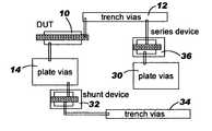
- FIG. 1illustrates a potentially damaged SOI transistor 10 that has its gate connected to a plate via 14 and its source/drain connected to a trench via 12 (or vice versa).
- the inventionidentifies this SOI transistor 10 as having the potential to be damaged because charge accumulation on the plate via 14 will be substantially different than the trench via 12 because the long narrow shape of the trench via-antenna 12 provides a greater antenna effect and will accumulate a more positive potential than will the plate via-antenna 14 .
- the inventionadds a shunt device 20 connected to either the source/drain or gate.
- the shunt deviceis, for example, a diode-connected transistor that has its gate tied to its source.
- the structurecan also include a compensating conductor 30 connected through an additional series device 36 as shown in FIG. 3 .
- the inventioncan add more series devices 32 and potentially more conductive features 34 , if needed, in order to balance the charging effects.
- the shunt deviceshould be positioned in parallel with the SOI transistor.
- the shunt devicecan be positioned between a first conductor connected to the source/drain of the SOI transistor and a second conductor connected to the gate of the SOI transistor.
- a series devicecan be positioned between a first conductor connected to the SOI transistor and a second conductor (e.g., 30 , 34 ) that is not connected to the SOI transistor.
- the inventioncan further include additional series devices (e.g., 32 , 36 ), wherein the first series device is connected to a first conductor and the second series device is connected to a second conductor, where the first conductor is connected to the source/drain of the SOI transistor and the second conductor is connected to the gate of the SOI transistor.
- additional series devicese.g., 32 , 36
- the designermay choose the most appropriate means of eliminating the potential for damage. For example, a very large damage-susceptible device may be readily protected by the addition of a shunt device, where the additional leakage across the shunt device will not affect normal circuit operation. For locations where the leakage is unacceptable, a compensating antenna may be added. Additional capacitive load is the penalty for this approach. For locations where neither leakage nor capacitive load is acceptable to the normal circuit operation, connection of the compensating antenna through the series device is the best option.
- the additional conductive features 30 , 34 and series devices 32 , 36 shown in FIG. 3are merely exemplary devices added by the application. These examples primarily add the series devices and conductive features to balance the antenna affects due to via configuration differences. Series devices and conductive features may be added to compensate for other differences such as proximity of conductive lines, uneven positioning within the chip, etc. In addition, other devices such as large FETs can be added to compensate for other unbalances, including parasitic capacitance.
- the compensating devices and conductive shapesare added to the circuit to eliminate the potential for charging damage between the source/drain and the gate of the SOI transistor. Further, these devices and compensating structures perform no function other than eliminating the potential for charging damage.
- the inventionprovides rapid design flow from the checking algorithm and repair options provided, increased flexibility in choice of processes and tooling that might damage less robustly designed products, and improved reliability and yield in damage-free SOI products.
Landscapes
- Semiconductor Integrated Circuits (AREA)
- Thin Film Transistor (AREA)
Abstract
Description
- 1. Field of the Invention
- The present invention generally relates to protection circuitry and more particularly to a method and structure that includes a shunt device between the source/drain and gate of SOI transistors which may develop a voltage differential between the source/drain and gate during wafer fabrication. The shunt device eliminates the potential for charging damage from processing.
- 2. Description of Related Art
- One problem that exists when designing integrated circuits with silicon-over-insulator (SOI) transistors relates to the detection of which SOI transistors may be susceptible to charging damage, and to providing protection once such a susceptible device is identified. In SOI it is not possible to “tie down” a floating gate in the traditional sense, such as by adding a diode connection to the substrate or nwell. SOI technologies are inherently less susceptible to charging damage because both the source/drain and the gate tend to have similar antennae, so the potential of both nodes varies together. This is not, however, certain in all cases. The invention described below is designed to detect and modify the integrated circuit design to eliminate the possibility of charging damage.
- The invention provides a method of altering an integrated circuit design having silicon over insulator (SOI) transistors. The invention prevents damage from a potential difference between the source/drain and gate of SOI transistors by tracing electrical nets in the integrated circuit design, identifying SOI transistors that may have a voltage differential between the source/drain and gate as potentially damaged SOI transistors (based on the tracing of the electrical nets), and connecting a shunt device across the source/drain and the gate of each of the potentially damaged SOI transistors. In addition, the invention can also connect compensating antennae to each of the nodes to balance the charging and eliminate the potential for damage.
- The shunt device and the compensating conductor eliminate the potential for charging damage to the gate of each of the potentially damaged SOI transistors. The tracing process is performed assuming all metals and diffusions are conductive. The tracing, the identifying, and the connecting processes are repeated at each level of wiring within the integrated circuit design.
- The invention compares aspect ratios of vias connected to the source/drain and the gate of each of the SOI transistors to determine whether a voltage differential might exist between the source/drain and the gate. Alternatively, the invention can compare chip locations of conductors connected to the source/drain and the gate of each of the SOI transistors to determine whether a voltage differential might exist between the source/drain and the gate. Also, the invention can compare parasitic capacitances of conductors connected to the source/drain and the gate of each of the SOI transistors to determine whether a voltage differential might exist between the source/drain and the gate.
- The foregoing process produces a protection circuit for an integrated circuit device that includes silicon over insulator (SOI) transistors and has a shunt device connected from the source/drain to the gate of at least one of the SOI transistors. The structure can also include a compensating conductor connected to one or the other or both of the source/drain or gate of the susceptible device through a series device. The series device and the compensating conductor eliminate the potential for charging damage between the source/drain and the gate of the SOI transistor. Further, the shunt and the series devices perform no function other than eliminating the potential for charging damage. The shunt and series device could be, for example, an FET connected as a diode.
- The shunt device should be positioned in parallel with the SOI transistor. Thus, the shunt device can be positioned between a first conductor connected to the source/drain of the SOI transistor and a second conductor connected to the gate of the SOI transistor. Alternatively, the series device can be positioned between a first conductor connected to the SOI transistor and a second conductor that is not connected to the SOI transistor. Also, the invention can further include a second shunt device, wherein the shunt device is connected to a first conductor and the second shunt device is connected to a second conductor, where the first conductor is connected to the source/drain of the SOI transistor and the second conductor is connected to the gate of the SOI transistor.
- These, and other, aspects and objects of the present invention will be better appreciated and understood when considered in conjunction with the following description and the accompanying drawings. It should be understood, however, that the following description, while indicating preferred embodiments of the present invention and numerous specific details thereof, is given by way of illustration and not of limitation. Many changes and modifications may be made within the scope of the present invention without departing from the spirit thereof, and the invention includes all such modifications.
- The invention will be better understood from the following detailed description with reference to the drawings, in which:
FIG. 1 is a schematic diagram of a SOI circuit;FIG. 2 is a schematic diagram of a SOI circuit with a shunt;FIG. 3 is a schematic diagram of a SOI circuit with series devices; andFIG. 4 is a flow diagram illustrating a method of the invention.- The present invention and the various features and advantageous details thereof are explained more fully with reference to the nonlimiting embodiments that are illustrated in the accompanying drawings and detailed in the following description. It should be noted that the features illustrated in the drawings are not necessarily drawn to scale. Descriptions of well-known components and processing techniques are omitted so as to not unnecessarily obscure the present invention in detail. The examples used herein are intended merely to facilitate an understanding of ways in which the invention may be practiced and to further enable those of skill in the art to practice the invention. Accordingly, the examples should not be construed as limiting the scope of the invention.
- As mentioned above, even SOI design structures produce the possibility of charging damage. For example, it is possible to create a differential antenna by the arrangement of vias within the metal line. Vias placed in narrow metal lines have a larger aspect ratio than vias placed well within large metal plates, and may therefore charge to a different potential when exposed to a plasma. This occurs in either via-first or trough-first processes, although the specific sensitive process then varies. If the gate and source/drain have different via/metal configurations, then charging damage can occur.
- To address this problem, the invention traces electrical nets assuming that metals and diffusions (even when they are cut by an FET gate) are conductive, determines the characteristics of the charge-collecting antennas on each node of each FET, assesses the potential for charging damage on each device. Where appropriate, a shunt device and/or a compensating antenna, perhaps connected through a series device, is placed to eliminate the potential for charging damage.
- More specifically, the vias on each node (gate and source/drain) of each FET are categorized and counted. The source and drain of each transistor have the same potential during the processing. Therefore, the source and drain are considered synonymous in this application and are sometimes referred to herein as a single unit using the terminology “source/drain.” The conductive connections to the gate and source/drain are identified as either a high-aspect ratio or low-aspect ratio via by examining their shapes and locations with respect to the edge of the metal wire. The effective net on each node is determined by considering all FETs to be conductive (this is a realistic assumption as there is large leakage from each source/drain to the floating well, particularly under the typical processing conditions of elevated temperature and in the presence of photons). If the two nodes are in fact on the same net (assuming conductive FETs) then the device is not considered to be subject to damage. The potential for charging damage is assessed by considering how different and how large the antennas on the two nodes are. If the possibility of damage is considered to be too large, then a shunt device may be inserted from gate to source/drain, the antenna on one or the other of the nodes may be redesigned to balance the charging, or an additional dummy antenna may be added to one or the other node to balance the design. The dummy antenna may be connected with an otherwise non-functional transistor as a “series device.”
- During processing, the ultimate circuit configuration is not complete, so at each level of wiring (M1, M2, etc.) the charging situation is re-assessed. The total number of nodes to be examined reduces as higher levels of wiring are considered, until there is effectively only one single node at the final wiring level. Various degrees of refinement are possible, depending on the specifics of the particular technology. For example, the damage may be observed to occur only on devices of a particular type, and in a particular configuration. One such example is that “thick”(>2 nm) pfets with high-aspect ratio vias on the gate node may be the only susceptible configuration, and all others may be safely ignored.
FIG. 4 shows of the invention in flowchart form. More specifically,FIG. 4 shows that the invention prevents damage from current flow between the source/drain and gate of SOI transistors by tracing electrical nets in theintegrated circuit design 40, identifying SOI transistors that may have a voltage differential between the source/drain and gate as potentially damaged SOI transistors42 (based on the tracing of the electrical nets), and connecting a shunt device to one of the source/drain and the gate of each of the potentially damagedSOI transistors 44. In addition, the invention can also connect compensating conductors to the potentially damaged transistor, possibly throughseries device 46. The series device and the compensating conductor eliminate the potential for charging damage between the source/drain and the gate of each of the potentially damaged SOI transistors. As mentioned above, the tracing process is performed assuming all metals and diffusions are conductive. Further, the tracing, the identifying, and the connecting processes are repeated at each level of wiring within the integrated circuit design.- The invention uses a number of different processes to determine whether a voltage differential may exist between the source/drain and gate of each SOI transistor. For example, the invention compares aspect ratios of vias connected to the source/drain and the gate of each of the SOI transistors to determine whether a voltage differential may exist between the source/drain and the gate. As mentioned above, the physical design of the conductive shapes that are connected to the gate and source/drain are compared to determine if such conductive shapes will act in similar manners as antennae with respect to charge accumulation. This can be accomplished using any conventional shapes processing program. Therefore, the invention obtains the length, width, height, etc. dimensions of the various conductors from the conventional shapes processing program and compares these different shapes. For example, a via embedded in a long thin metal wire will have different antenna characteristics than a via within a wide plate. If the shapes are not balanced, the charge accumulation is not likely to be balanced.
- In addition, the invention can compare chip locations of conductors connected to the source/drain and the gate of each of the SOI transistors to determine whether a voltage differential may exist between the source/drain and the gate. Again, using any conventional integrated circuit model program the location, direction, length, etc. of the conductors connected to the gate and to the source/drain are compared to determine whether their different positions within the chip (or circuit) would cause a voltage differential. Further, the proximity of other conductive lines is considered by the invention. Therefore, other conductive lines that are within a predetermined proximity (and/or that carry a predetermined voltage level) will be considered to leak a certain predetermined percentage of the voltage to the conductor in question. Also, the invention can compare parasitic capacitances of conductors connected to the source/drain and the gate of each of the SOI transistors to determine whether a voltage differential may exist between the source/drain and the gate. Thus, the invention uses any conventional parasitic capacitance calculator to determine the parasitic capacitance of a conductor connected to the gate and compares this parasitic capacitance to a conductor connected to the source/drain.
- For example,
FIG. 1 illustrates a potentially damagedSOI transistor 10 that has its gate connected to a plate via14 and its source/drain connected to a trench via12 (or vice versa). As mentioned above, the invention identifies thisSOI transistor 10 as having the potential to be damaged because charge accumulation on the plate via14 will be substantially different than the trench via12 because the long narrow shape of the trench via-antenna 12 provides a greater antenna effect and will accumulate a more positive potential than will the plate via-antenna 14. As shown inFIG. 2 , the invention adds ashunt device 20 connected to either the source/drain or gate. The shunt device is, for example, a diode-connected transistor that has its gate tied to its source. The structure can also include a compensatingconductor 30 connected through anadditional series device 36 as shown inFIG. 3 . Also, the invention can addmore series devices 32 and potentially moreconductive features 34, if needed, in order to balance the charging effects. - As shown in
FIG. 2 , the shunt device should be positioned in parallel with the SOI transistor. Thus, the shunt device can be positioned between a first conductor connected to the source/drain of the SOI transistor and a second conductor connected to the gate of the SOI transistor. Alternatively, a series device can be positioned between a first conductor connected to the SOI transistor and a second conductor (e.g.,30,34) that is not connected to the SOI transistor. Also, the invention can further include additional series devices (e.g.,32,36), wherein the first series device is connected to a first conductor and the second series device is connected to a second conductor, where the first conductor is connected to the source/drain of the SOI transistor and the second conductor is connected to the gate of the SOI transistor. - Once the susceptible devices are identified by the tracing program, the designer may choose the most appropriate means of eliminating the potential for damage. For example, a very large damage-susceptible device may be readily protected by the addition of a shunt device, where the additional leakage across the shunt device will not affect normal circuit operation. For locations where the leakage is unacceptable, a compensating antenna may be added. Additional capacitive load is the penalty for this approach. For locations where neither leakage nor capacitive load is acceptable to the normal circuit operation, connection of the compensating antenna through the series device is the best option.
- The additional
conductive features series devices FIG. 3 are merely exemplary devices added by the application. These examples primarily add the series devices and conductive features to balance the antenna affects due to via configuration differences. Series devices and conductive features may be added to compensate for other differences such as proximity of conductive lines, uneven positioning within the chip, etc. In addition, other devices such as large FETs can be added to compensate for other unbalances, including parasitic capacitance. The compensating devices and conductive shapes are added to the circuit to eliminate the potential for charging damage between the source/drain and the gate of the SOI transistor. Further, these devices and compensating structures perform no function other than eliminating the potential for charging damage. The invention provides rapid design flow from the checking algorithm and repair options provided, increased flexibility in choice of processes and tooling that might damage less robustly designed products, and improved reliability and yield in damage-free SOI products. - While the invention has been described in terms of preferred embodiments, those skilled in the art will recognize that the invention can be practiced with modification within the spirit and scope of the appended claims.
Claims (17)
Priority Applications (4)
| Application Number | Priority Date | Filing Date | Title |
|---|---|---|---|
| US10/605,888US7067886B2 (en) | 2003-11-04 | 2003-11-04 | Method of assessing potential for charging damage in SOI designs and structures for eliminating potential for damage |
| US11/003,988US7132318B2 (en) | 2003-11-04 | 2004-12-04 | Method of assessing potential for charging damage in SOI designs and structures for eliminating potential for damage |
| US11/275,482US7470959B2 (en) | 2003-11-04 | 2006-01-09 | Integrated circuit structures for preventing charging damage |
| US11/749,775US7560345B2 (en) | 2003-11-04 | 2007-05-17 | Method of assessing potential for charging damage in integrated circuit designs and structures for preventing charging damage |
Applications Claiming Priority (1)
| Application Number | Priority Date | Filing Date | Title |
|---|---|---|---|
| US10/605,888US7067886B2 (en) | 2003-11-04 | 2003-11-04 | Method of assessing potential for charging damage in SOI designs and structures for eliminating potential for damage |
Related Child Applications (1)
| Application Number | Title | Priority Date | Filing Date |
|---|---|---|---|
| US11/003,988DivisionUS7132318B2 (en) | 2003-11-04 | 2004-12-04 | Method of assessing potential for charging damage in SOI designs and structures for eliminating potential for damage |
Publications (2)
| Publication Number | Publication Date |
|---|---|
| US20050093072A1true US20050093072A1 (en) | 2005-05-05 |
| US7067886B2 US7067886B2 (en) | 2006-06-27 |
Family
ID=34549683
Family Applications (2)
| Application Number | Title | Priority Date | Filing Date |
|---|---|---|---|
| US10/605,888Expired - Fee RelatedUS7067886B2 (en) | 2003-11-04 | 2003-11-04 | Method of assessing potential for charging damage in SOI designs and structures for eliminating potential for damage |
| US11/003,988Expired - Fee RelatedUS7132318B2 (en) | 2003-11-04 | 2004-12-04 | Method of assessing potential for charging damage in SOI designs and structures for eliminating potential for damage |
Family Applications After (1)
| Application Number | Title | Priority Date | Filing Date |
|---|---|---|---|
| US11/003,988Expired - Fee RelatedUS7132318B2 (en) | 2003-11-04 | 2004-12-04 | Method of assessing potential for charging damage in SOI designs and structures for eliminating potential for damage |
Country Status (1)
| Country | Link |
|---|---|
| US (2) | US7067886B2 (en) |
Cited By (30)
| Publication number | Priority date | Publication date | Assignee | Title |
|---|---|---|---|---|
| US20090026082A1 (en)* | 2006-12-14 | 2009-01-29 | Ion Torrent Systems Incorporated | Methods and apparatus for measuring analytes using large scale FET arrays |
| US20100197507A1 (en)* | 2006-12-14 | 2010-08-05 | Ion Torrent Systems Incorporated | Methods and apparatus for measuring analytes using large scale fet arrays |
| US8217433B1 (en) | 2010-06-30 | 2012-07-10 | Life Technologies Corporation | One-transistor pixel array |
| US8263336B2 (en) | 2009-05-29 | 2012-09-11 | Life Technologies Corporation | Methods and apparatus for measuring analytes |
| US20130005096A1 (en)* | 2011-07-01 | 2013-01-03 | Samsung Electronics Co., Ltd. | Semiconductor device and method of fabricating the same |
| US8349167B2 (en) | 2006-12-14 | 2013-01-08 | Life Technologies Corporation | Methods and apparatus for detecting molecular interactions using FET arrays |
| US8470164B2 (en) | 2008-06-25 | 2013-06-25 | Life Technologies Corporation | Methods and apparatus for measuring analytes using large scale FET arrays |
| US8653567B2 (en) | 2010-07-03 | 2014-02-18 | Life Technologies Corporation | Chemically sensitive sensor with lightly doped drains |
| US8673627B2 (en) | 2009-05-29 | 2014-03-18 | Life Technologies Corporation | Apparatus and methods for performing electrochemical reactions |
| US8685324B2 (en) | 2010-09-24 | 2014-04-01 | Life Technologies Corporation | Matched pair transistor circuits |
| US8747748B2 (en) | 2012-01-19 | 2014-06-10 | Life Technologies Corporation | Chemical sensor with conductive cup-shaped sensor surface |
| US8753812B2 (en) | 2004-11-12 | 2014-06-17 | The Board Of Trustees Of The Leland Stanford Junior University | Charge perturbation detection method for DNA and other molecules |
| US8776573B2 (en) | 2009-05-29 | 2014-07-15 | Life Technologies Corporation | Methods and apparatus for measuring analytes |
| US8821798B2 (en) | 2012-01-19 | 2014-09-02 | Life Technologies Corporation | Titanium nitride as sensing layer for microwell structure |
| US8858782B2 (en) | 2010-06-30 | 2014-10-14 | Life Technologies Corporation | Ion-sensing charge-accumulation circuits and methods |
| US8936763B2 (en) | 2008-10-22 | 2015-01-20 | Life Technologies Corporation | Integrated sensor arrays for biological and chemical analysis |
| US9080968B2 (en) | 2013-01-04 | 2015-07-14 | Life Technologies Corporation | Methods and systems for point of use removal of sacrificial material |
| US9109251B2 (en) | 2004-06-25 | 2015-08-18 | University Of Hawaii | Ultrasensitive biosensors |
| US9270264B2 (en) | 2012-05-29 | 2016-02-23 | Life Technologies Corporation | System for reducing noise in a chemical sensor array |
| US9618475B2 (en) | 2010-09-15 | 2017-04-11 | Life Technologies Corporation | Methods and apparatus for measuring analytes |
| US9835585B2 (en) | 2013-03-15 | 2017-12-05 | Life Technologies Corporation | Chemical sensor with protruded sensor surface |
| US9841398B2 (en) | 2013-01-08 | 2017-12-12 | Life Technologies Corporation | Methods for manufacturing well structures for low-noise chemical sensors |
| US9970984B2 (en) | 2011-12-01 | 2018-05-15 | Life Technologies Corporation | Method and apparatus for identifying defects in a chemical sensor array |
| US9995708B2 (en) | 2013-03-13 | 2018-06-12 | Life Technologies Corporation | Chemical sensor with sidewall spacer sensor surface |
| US10100357B2 (en) | 2013-05-09 | 2018-10-16 | Life Technologies Corporation | Windowed sequencing |
| US10422767B2 (en) | 2013-03-15 | 2019-09-24 | Life Technologies Corporation | Chemical sensor with consistent sensor surface areas |
| US10458942B2 (en) | 2013-06-10 | 2019-10-29 | Life Technologies Corporation | Chemical sensor array having multiple sensors per well |
| US10767224B2 (en) | 2014-12-18 | 2020-09-08 | Life Technologies Corporation | High data rate integrated circuit with power management |
| US11307166B2 (en) | 2010-07-01 | 2022-04-19 | Life Technologies Corporation | Column ADC |
| FR3123501A1 (en)* | 2021-05-25 | 2022-12-02 | Stmicroelectronics Sa | Passive electrostatic discharge sensor and method for detecting electrostatic discharges. |
Families Citing this family (17)
| Publication number | Priority date | Publication date | Assignee | Title |
|---|---|---|---|---|
| US7470959B2 (en)* | 2003-11-04 | 2008-12-30 | International Business Machines Corporation | Integrated circuit structures for preventing charging damage |
| US20070271540A1 (en)* | 2006-05-16 | 2007-11-22 | International Business Machines Corporation | Structure and method for reducing susceptibility to charging damage in soi designs |
| US11339430B2 (en) | 2007-07-10 | 2022-05-24 | Life Technologies Corporation | Methods and apparatus for measuring analytes using large scale FET arrays |
| US7712057B2 (en)* | 2007-12-13 | 2010-05-04 | International Business Machines Corporation | Determining allowance antenna area as function of total gate insulator area for SOI technology |
| US20120261274A1 (en) | 2009-05-29 | 2012-10-18 | Life Technologies Corporation | Methods and apparatus for measuring analytes |
| TWI539172B (en) | 2010-06-30 | 2016-06-21 | 生命技術公司 | Methods and apparatus for testing isfet arrays |
| US8962366B2 (en) | 2013-01-28 | 2015-02-24 | Life Technologies Corporation | Self-aligned well structures for low-noise chemical sensors |
| US8841217B1 (en) | 2013-03-13 | 2014-09-23 | Life Technologies Corporation | Chemical sensor with protruded sensor surface |
| EP2972279B1 (en) | 2013-03-15 | 2021-10-06 | Life Technologies Corporation | Chemical sensors with consistent sensor surface areas |
| JP6671274B2 (en) | 2013-03-15 | 2020-03-25 | ライフ テクノロジーズ コーポレーション | Chemical device with thin conductive element |
| US9116117B2 (en) | 2013-03-15 | 2015-08-25 | Life Technologies Corporation | Chemical sensor with sidewall sensor surface |
| CN107407656B (en) | 2014-12-18 | 2020-04-07 | 生命科技公司 | Method and apparatus for measuring analytes using large scale FET arrays |
| KR102593647B1 (en) | 2014-12-18 | 2023-10-26 | 라이프 테크놀로지스 코포레이션 | High data rate integrated circuit with transmitter configuration |
| US9378329B1 (en) | 2015-05-08 | 2016-06-28 | International Business Machines Corporation | Immunity to inline charging damage in circuit designs |
| US9990459B2 (en) | 2016-03-18 | 2018-06-05 | International Business Machines Corporation | Checking wafer-level integrated designs for antenna rule compliance |
| US10346580B2 (en) | 2016-03-25 | 2019-07-09 | International Business Machines Corporation | Checking wafer-level integrated designs for rule compliance |
| US10002800B2 (en) | 2016-05-13 | 2018-06-19 | International Business Machines Corporation | Prevention of charging damage in full-depletion devices |
Citations (26)
| Publication number | Priority date | Publication date | Assignee | Title |
|---|---|---|---|---|
| US5923067A (en)* | 1997-04-04 | 1999-07-13 | International Business Machines Corporation | 3-D CMOS-on-SOI ESD structure and method |
| US5994742A (en)* | 1995-12-08 | 1999-11-30 | Texas Instruments Incorporated | Plasma emission triggered protection device for protecting against charge-induced damage |
| US5998299A (en)* | 1996-12-09 | 1999-12-07 | Texas Instruments Incorporated | Protection structures for the suppression of plasma damage |
| US6016062A (en)* | 1995-10-13 | 2000-01-18 | Texas Instruments Incorporated | Process related damage monitor (predator)--systematic variation of antenna parameters to determine charge damage |
| US6194233B1 (en)* | 1998-08-21 | 2001-02-27 | International Business Machines Corporation | Integrated circuit and method of manufacture for avoiding damage by electrostatic charge |
| US6207996B1 (en)* | 1998-11-30 | 2001-03-27 | Seiko Instuments Inc. | Semiconductor device and method for manufacturing the same |
| US6235642B1 (en)* | 2000-01-14 | 2001-05-22 | United Microelectronics Corporation | Method for reducing plasma charging damages |
| US20010006243A1 (en)* | 1999-12-27 | 2001-07-05 | Yasuyuki Morishita | Input-output protection device for semiconductor integrated circuit |
| US6292927B1 (en)* | 1998-12-07 | 2001-09-18 | Artisan Components, Inc. | Reduction of process antenna effects in integrated circuits |
| US20010028056A1 (en)* | 2000-04-05 | 2001-10-11 | Matsushita Electronics Corporation | Evaluation method of semiconductor chargeup damage and apparatus therefor |
| US20010045667A1 (en)* | 2000-04-21 | 2001-11-29 | Hiroshi Yamauchi | Semiconductor device and process of manufacturing the same |
| US20010046718A1 (en)* | 1997-03-31 | 2001-11-29 | Ali Akbar Iranmanesh | Method and apparatus for reducing process-induced charge buildup |
| US20020000579A1 (en)* | 1999-10-06 | 2002-01-03 | Fujitsu Limited | Semiconductor device having a gate insulation film resistant to dielectric breakdown. |
| US20020031617A1 (en)* | 2000-09-12 | 2002-03-14 | Masahiro Sumiya | Plasma processing apparatus and method with controlled biasing functions |
| US20020037651A1 (en)* | 1999-11-12 | 2002-03-28 | Tzung-Han Lee | Method for minimizing damage of process charging phenomena |
| US20020050617A1 (en)* | 2000-10-30 | 2002-05-02 | Oki Electric Industry Co., Ltd. | Semiconductor device |
| US20020063298A1 (en)* | 2000-11-29 | 2002-05-30 | United Microelectronics Corp. | Semiconductor device for preventing process-induced charging damages |
| US6414358B1 (en)* | 2001-09-28 | 2002-07-02 | Intel Corporation | Arrangements to reduce charging damage in structures of integrated circuits |
| US6417544B1 (en)* | 2001-06-11 | 2002-07-09 | Chartered Semiconductor Manufacturing Ltd. | Diode-like plasma induced damage protection structure |
| US20020096723A1 (en)* | 1999-12-31 | 2002-07-25 | Kaoru Awaka | Transient frequency in dynamic threshold metal-oxide-semiconductor field effect transistors |
| US20020142526A1 (en)* | 2001-03-30 | 2002-10-03 | International Business Machines Corporation | Structures and methods to minimize plasma charging damage in silicon on insulator devices |
| US20020158348A1 (en)* | 2001-04-27 | 2002-10-31 | Motorola, Inc. | Semiconductor structure and method for reducing charge damage |
| US6504212B1 (en)* | 2000-02-03 | 2003-01-07 | International Business Machines Corporation | Method and apparatus for enhanced SOI passgate operations |
| US20030068878A1 (en)* | 2001-09-28 | 2003-04-10 | Lin Wallace W. | Arrangements to reduce charging damage in structures of integrated circuits |
| US20030075762A1 (en)* | 2001-09-28 | 2003-04-24 | Lin Wallace W. | Arrangements to reduce charging damage in structures of integrated circuits |
| US20030114015A1 (en)* | 1999-04-07 | 2003-06-19 | Ken Tokashiki | Apparatus for fabricating a semiconductor device and method of doing the same |
Family Cites Families (1)
| Publication number | Priority date | Publication date | Assignee | Title |
|---|---|---|---|---|
| JP2004235199A (en)* | 2003-01-28 | 2004-08-19 | Renesas Technology Corp | Semiconductor device |
- 2003
- 2003-11-04USUS10/605,888patent/US7067886B2/ennot_activeExpired - Fee Related
- 2004
- 2004-12-04USUS11/003,988patent/US7132318B2/ennot_activeExpired - Fee Related
Patent Citations (30)
| Publication number | Priority date | Publication date | Assignee | Title |
|---|---|---|---|---|
| US6016062A (en)* | 1995-10-13 | 2000-01-18 | Texas Instruments Incorporated | Process related damage monitor (predator)--systematic variation of antenna parameters to determine charge damage |
| US5994742A (en)* | 1995-12-08 | 1999-11-30 | Texas Instruments Incorporated | Plasma emission triggered protection device for protecting against charge-induced damage |
| US5998299A (en)* | 1996-12-09 | 1999-12-07 | Texas Instruments Incorporated | Protection structures for the suppression of plasma damage |
| US20030027399A1 (en)* | 1997-03-31 | 2003-02-06 | Iranmanesh Ali Akbar | Method and apparatus for reducing process-induced charge buildup |
| US20010046718A1 (en)* | 1997-03-31 | 2001-11-29 | Ali Akbar Iranmanesh | Method and apparatus for reducing process-induced charge buildup |
| US5923067A (en)* | 1997-04-04 | 1999-07-13 | International Business Machines Corporation | 3-D CMOS-on-SOI ESD structure and method |
| US6194233B1 (en)* | 1998-08-21 | 2001-02-27 | International Business Machines Corporation | Integrated circuit and method of manufacture for avoiding damage by electrostatic charge |
| US6207996B1 (en)* | 1998-11-30 | 2001-03-27 | Seiko Instuments Inc. | Semiconductor device and method for manufacturing the same |
| US6292927B1 (en)* | 1998-12-07 | 2001-09-18 | Artisan Components, Inc. | Reduction of process antenna effects in integrated circuits |
| US20030114015A1 (en)* | 1999-04-07 | 2003-06-19 | Ken Tokashiki | Apparatus for fabricating a semiconductor device and method of doing the same |
| US20020000579A1 (en)* | 1999-10-06 | 2002-01-03 | Fujitsu Limited | Semiconductor device having a gate insulation film resistant to dielectric breakdown. |
| US20020037651A1 (en)* | 1999-11-12 | 2002-03-28 | Tzung-Han Lee | Method for minimizing damage of process charging phenomena |
| US20010006243A1 (en)* | 1999-12-27 | 2001-07-05 | Yasuyuki Morishita | Input-output protection device for semiconductor integrated circuit |
| US20020096723A1 (en)* | 1999-12-31 | 2002-07-25 | Kaoru Awaka | Transient frequency in dynamic threshold metal-oxide-semiconductor field effect transistors |
| US6235642B1 (en)* | 2000-01-14 | 2001-05-22 | United Microelectronics Corporation | Method for reducing plasma charging damages |
| US6504212B1 (en)* | 2000-02-03 | 2003-01-07 | International Business Machines Corporation | Method and apparatus for enhanced SOI passgate operations |
| US20010028056A1 (en)* | 2000-04-05 | 2001-10-11 | Matsushita Electronics Corporation | Evaluation method of semiconductor chargeup damage and apparatus therefor |
| US6441397B2 (en)* | 2000-04-05 | 2002-08-27 | Matsushita Electronics Corporation | Evaluation of semiconductor chargeup damage and apparatus therefor |
| US20010045667A1 (en)* | 2000-04-21 | 2001-11-29 | Hiroshi Yamauchi | Semiconductor device and process of manufacturing the same |
| US20020031617A1 (en)* | 2000-09-12 | 2002-03-14 | Masahiro Sumiya | Plasma processing apparatus and method with controlled biasing functions |
| US20020050617A1 (en)* | 2000-10-30 | 2002-05-02 | Oki Electric Industry Co., Ltd. | Semiconductor device |
| US6448599B1 (en)* | 2000-11-29 | 2002-09-10 | United Microelectronics Corp. | Semiconductor device for preventing process-induced charging damages |
| US20020063298A1 (en)* | 2000-11-29 | 2002-05-30 | United Microelectronics Corp. | Semiconductor device for preventing process-induced charging damages |
| US20020142526A1 (en)* | 2001-03-30 | 2002-10-03 | International Business Machines Corporation | Structures and methods to minimize plasma charging damage in silicon on insulator devices |
| US20020158348A1 (en)* | 2001-04-27 | 2002-10-31 | Motorola, Inc. | Semiconductor structure and method for reducing charge damage |
| US6417544B1 (en)* | 2001-06-11 | 2002-07-09 | Chartered Semiconductor Manufacturing Ltd. | Diode-like plasma induced damage protection structure |
| US6414358B1 (en)* | 2001-09-28 | 2002-07-02 | Intel Corporation | Arrangements to reduce charging damage in structures of integrated circuits |
| US20030068878A1 (en)* | 2001-09-28 | 2003-04-10 | Lin Wallace W. | Arrangements to reduce charging damage in structures of integrated circuits |
| US20030075762A1 (en)* | 2001-09-28 | 2003-04-24 | Lin Wallace W. | Arrangements to reduce charging damage in structures of integrated circuits |
| US6566716B2 (en)* | 2001-09-28 | 2003-05-20 | Intel Corporation | Arrangements to reduce charging damage in structures of integrated circuits using polysilicon or metal plate(s) |
Cited By (106)
| Publication number | Priority date | Publication date | Assignee | Title |
|---|---|---|---|---|
| US10563252B2 (en) | 2004-06-25 | 2020-02-18 | University Of Hawaii | Ultrasensitive biosensors |
| US9109251B2 (en) | 2004-06-25 | 2015-08-18 | University Of Hawaii | Ultrasensitive biosensors |
| US8753812B2 (en) | 2004-11-12 | 2014-06-17 | The Board Of Trustees Of The Leland Stanford Junior University | Charge perturbation detection method for DNA and other molecules |
| US9228971B2 (en) | 2004-11-12 | 2016-01-05 | The Board Of Trustees Of The Leland Stanford Junior University | Charge perturbation detection system for DNA and other molecules |
| US12139749B2 (en) | 2004-11-12 | 2024-11-12 | The Board Of Trustees Of The Leland Stanford Junior University | Charge perturbation detection system for DNA and other molecules |
| US10822641B2 (en) | 2004-11-12 | 2020-11-03 | The Board Of Trustees Of The Leland Stanford Junior University | Charge perturbation detection system for DNA and other molecules |
| US8313639B2 (en) | 2006-12-14 | 2012-11-20 | Life Technologies Corporation | Methods and apparatus for measuring analytes using large scale FET arrays |
| US8764969B2 (en) | 2006-12-14 | 2014-07-01 | Life Technologies Corporation | Methods for operating chemically sensitive sensors with sample and hold capacitors |
| US8262900B2 (en) | 2006-12-14 | 2012-09-11 | Life Technologies Corporation | Methods and apparatus for measuring analytes using large scale FET arrays |
| US8269261B2 (en) | 2006-12-14 | 2012-09-18 | Life Technologies Corporation | Methods and apparatus for measuring analytes using large scale FET arrays |
| US8293082B2 (en) | 2006-12-14 | 2012-10-23 | Life Technologies Corporation | Methods and apparatus for measuring analytes using large scale FET arrays |
| US8306757B2 (en) | 2006-12-14 | 2012-11-06 | Life Technologies Corporation | Methods and apparatus for measuring analytes using large scale FET arrays |
| US8658017B2 (en) | 2006-12-14 | 2014-02-25 | Life Technologies Corporation | Methods for operating an array of chemically-sensitive sensors |
| US8313625B2 (en) | 2006-12-14 | 2012-11-20 | Life Technologies Corporation | Methods and apparatus for measuring analytes using large scale FET arrays |
| US8317999B2 (en) | 2006-12-14 | 2012-11-27 | Life Technologies Corporation | Methods and apparatus for measuring analytes using large scale FET arrays |
| US9989489B2 (en) | 2006-12-14 | 2018-06-05 | Life Technnologies Corporation | Methods for calibrating an array of chemically-sensitive sensors |
| US8349167B2 (en) | 2006-12-14 | 2013-01-08 | Life Technologies Corporation | Methods and apparatus for detecting molecular interactions using FET arrays |
| US20090026082A1 (en)* | 2006-12-14 | 2009-01-29 | Ion Torrent Systems Incorporated | Methods and apparatus for measuring analytes using large scale FET arrays |
| US8415716B2 (en) | 2006-12-14 | 2013-04-09 | Life Technologies Corporation | Chemically sensitive sensors with feedback circuits |
| US9951382B2 (en) | 2006-12-14 | 2018-04-24 | Life Technologies Corporation | Methods and apparatus for measuring analytes using large scale FET arrays |
| US9404920B2 (en) | 2006-12-14 | 2016-08-02 | Life Technologies Corporation | Methods and apparatus for detecting molecular interactions using FET arrays |
| US8426898B2 (en) | 2006-12-14 | 2013-04-23 | Life Technologies Corporation | Methods and apparatus for measuring analytes using large scale FET arrays |
| US8426899B2 (en) | 2006-12-14 | 2013-04-23 | Life Technologies Corporation | Methods and apparatus for measuring analytes using large scale FET arrays |
| US20120129728A1 (en)* | 2006-12-14 | 2012-05-24 | Life Technologies Corporation | Methods and Apparatus for Measuring Analytes Using Large Scale FET Arrays |
| US20110230375A1 (en)* | 2006-12-14 | 2011-09-22 | Life Technologies Corporation | Methods and apparatus for measuring analytes using large scale fet arrays |
| US8435395B2 (en) | 2006-12-14 | 2013-05-07 | Life Technologies Corporation | Methods and apparatus for measuring analytes using large scale FET arrays |
| US8441044B2 (en) | 2006-12-14 | 2013-05-14 | Life Technologies Corporation | Methods for manufacturing low noise chemically-sensitive field effect transistors |
| US8445945B2 (en) | 2006-12-14 | 2013-05-21 | Life Technologies Corporation | Low noise chemically-sensitive field effect transistors |
| US8450781B2 (en) | 2006-12-14 | 2013-05-28 | Life Technologies Corporation | Methods and apparatus for measuring analytes using large scale FET arrays |
| US9039888B2 (en) | 2006-12-14 | 2015-05-26 | Life Technologies Corporation | Methods and apparatus for detecting molecular interactions using FET arrays |
| US8685230B2 (en) | 2006-12-14 | 2014-04-01 | Life Technologies Corporation | Methods and apparatus for high-speed operation of a chemically-sensitive sensor array |
| US20100197507A1 (en)* | 2006-12-14 | 2010-08-05 | Ion Torrent Systems Incorporated | Methods and apparatus for measuring analytes using large scale fet arrays |
| US8492800B2 (en) | 2006-12-14 | 2013-07-23 | Life Technologies Corporation | Chemically sensitive sensors with sample and hold capacitors |
| US8492799B2 (en) | 2006-12-14 | 2013-07-23 | Life Technologies Corporation | Methods and apparatus for detecting molecular interactions using FET arrays |
| US8496802B2 (en) | 2006-12-14 | 2013-07-30 | Life Technologies Corporation | Methods for operating chemically-sensitive sample and hold sensors |
| US8502278B2 (en) | 2006-12-14 | 2013-08-06 | Life Technologies Corporation | Chemically-sensitive sample and hold sensors |
| US8519448B2 (en) | 2006-12-14 | 2013-08-27 | Life Technologies Corporation | Chemically-sensitive array with active and reference sensors |
| US8264014B2 (en)* | 2006-12-14 | 2012-09-11 | Life Technologies Corporation | Methods and apparatus for measuring analytes using large scale FET arrays |
| US8575664B2 (en) | 2006-12-14 | 2013-11-05 | Life Technologies Corporation | Chemically-sensitive sensor array calibration circuitry |
| US8530941B2 (en) | 2006-12-14 | 2013-09-10 | Life Technologies Corporation | Methods and apparatus for measuring analytes using large scale FET arrays |
| US8535513B2 (en) | 2006-12-14 | 2013-09-17 | Life Technologies Corporation | Methods and apparatus for measuring analytes using large scale FET arrays |
| US8540867B2 (en) | 2006-12-14 | 2013-09-24 | Life Technologies Corporation | Methods and apparatus for detecting molecular interactions using FET arrays |
| US8540866B2 (en) | 2006-12-14 | 2013-09-24 | Life Technologies Corporation | Methods and apparatus for detecting molecular interactions using FET arrays |
| US8540865B2 (en) | 2006-12-14 | 2013-09-24 | Life Technologies Corporation | Methods and apparatus for detecting molecular interactions using FET arrays |
| US8540868B2 (en) | 2006-12-14 | 2013-09-24 | Life Technologies Corporation | Methods and apparatus for detecting molecular interactions using FET arrays |
| US8558288B2 (en) | 2006-12-14 | 2013-10-15 | Life Technologies Corporation | Methods and apparatus for measuring analytes using large scale FET arrays |
| US8524057B2 (en) | 2008-06-25 | 2013-09-03 | Life Technologies Corporation | Methods and apparatus for measuring analytes using large scale FET arrays |
| US8470164B2 (en) | 2008-06-25 | 2013-06-25 | Life Technologies Corporation | Methods and apparatus for measuring analytes using large scale FET arrays |
| US8936763B2 (en) | 2008-10-22 | 2015-01-20 | Life Technologies Corporation | Integrated sensor arrays for biological and chemical analysis |
| US9964515B2 (en) | 2008-10-22 | 2018-05-08 | Life Technologies Corporation | Integrated sensor arrays for biological and chemical analysis |
| US8673627B2 (en) | 2009-05-29 | 2014-03-18 | Life Technologies Corporation | Apparatus and methods for performing electrochemical reactions |
| US8776573B2 (en) | 2009-05-29 | 2014-07-15 | Life Technologies Corporation | Methods and apparatus for measuring analytes |
| US8592154B2 (en) | 2009-05-29 | 2013-11-26 | Life Technologies Corporation | Methods and apparatus for high speed operation of a chemically-sensitive sensor array |
| US8263336B2 (en) | 2009-05-29 | 2012-09-11 | Life Technologies Corporation | Methods and apparatus for measuring analytes |
| US8698212B2 (en) | 2009-05-29 | 2014-04-15 | Life Technologies Corporation | Active chemically-sensitive sensors |
| US9927393B2 (en) | 2009-05-29 | 2018-03-27 | Life Technologies Corporation | Methods and apparatus for measuring analytes |
| US8742469B2 (en) | 2009-05-29 | 2014-06-03 | Life Technologies Corporation | Active chemically-sensitive sensors with correlated double sampling |
| US8748947B2 (en) | 2009-05-29 | 2014-06-10 | Life Technologies Corporation | Active chemically-sensitive sensors with reset switch |
| US8994076B2 (en) | 2009-05-29 | 2015-03-31 | Life Technologies Corporation | Chemically-sensitive field effect transistor based pixel array with protection diodes |
| US8592153B1 (en) | 2009-05-29 | 2013-11-26 | Life Technologies Corporation | Methods for manufacturing high capacitance microwell structures of chemically-sensitive sensors |
| US8822205B2 (en) | 2009-05-29 | 2014-09-02 | Life Technologies Corporation | Active chemically-sensitive sensors with source follower amplifier |
| US8766327B2 (en) | 2009-05-29 | 2014-07-01 | Life Technologies Corporation | Active chemically-sensitive sensors with in-sensor current sources |
| US8432149B2 (en) | 2010-06-30 | 2013-04-30 | Life Technologies Corporation | Array column integrator |
| US8731847B2 (en) | 2010-06-30 | 2014-05-20 | Life Technologies Corporation | Array configuration and readout scheme |
| US8415177B2 (en) | 2010-06-30 | 2013-04-09 | Life Technologies Corporation | Two-transistor pixel array |
| US8823380B2 (en) | 2010-06-30 | 2014-09-02 | Life Technologies Corporation | Capacitive charge pump |
| US10641729B2 (en) | 2010-06-30 | 2020-05-05 | Life Technologies Corporation | Column ADC |
| US8524487B2 (en) | 2010-06-30 | 2013-09-03 | Life Technologies Corporation | One-transistor pixel array with cascoded column circuit |
| US8415176B2 (en) | 2010-06-30 | 2013-04-09 | Life Technologies Corporation | One-transistor pixel array |
| US8858782B2 (en) | 2010-06-30 | 2014-10-14 | Life Technologies Corporation | Ion-sensing charge-accumulation circuits and methods |
| US8487790B2 (en) | 2010-06-30 | 2013-07-16 | Life Technologies Corporation | Chemical detection circuit including a serializer circuit |
| US8421437B2 (en) | 2010-06-30 | 2013-04-16 | Life Technologies Corporation | Array column integrator |
| US8455927B2 (en) | 2010-06-30 | 2013-06-04 | Life Technologies Corporation | One-transistor pixel array with cascoded column circuit |
| US8247849B2 (en) | 2010-06-30 | 2012-08-21 | Life Technologies Corporation | Two-transistor pixel array |
| US8432150B2 (en) | 2010-06-30 | 2013-04-30 | Life Technologies Corporation | Methods for operating an array column integrator |
| US8772698B2 (en) | 2010-06-30 | 2014-07-08 | Life Technologies Corporation | CCD-based multi-transistor active pixel sensor array |
| US9164070B2 (en) | 2010-06-30 | 2015-10-20 | Life Technologies Corporation | Column adc |
| US8217433B1 (en) | 2010-06-30 | 2012-07-10 | Life Technologies Corporation | One-transistor pixel array |
| US9239313B2 (en) | 2010-06-30 | 2016-01-19 | Life Technologies Corporation | Ion-sensing charge-accumulation circuits and methods |
| US11307166B2 (en) | 2010-07-01 | 2022-04-19 | Life Technologies Corporation | Column ADC |
| US8653567B2 (en) | 2010-07-03 | 2014-02-18 | Life Technologies Corporation | Chemically sensitive sensor with lightly doped drains |
| US9960253B2 (en) | 2010-07-03 | 2018-05-01 | Life Technologies Corporation | Chemically sensitive sensor with lightly doped drains |
| US9618475B2 (en) | 2010-09-15 | 2017-04-11 | Life Technologies Corporation | Methods and apparatus for measuring analytes |
| US9958414B2 (en) | 2010-09-15 | 2018-05-01 | Life Technologies Corporation | Apparatus for measuring analytes including chemical sensor array |
| US9958415B2 (en) | 2010-09-15 | 2018-05-01 | Life Technologies Corporation | ChemFET sensor including floating gate |
| US9110015B2 (en) | 2010-09-24 | 2015-08-18 | Life Technologies Corporation | Method and system for delta double sampling |
| US8685324B2 (en) | 2010-09-24 | 2014-04-01 | Life Technologies Corporation | Matched pair transistor circuits |
| US8796036B2 (en) | 2010-09-24 | 2014-08-05 | Life Technologies Corporation | Method and system for delta double sampling |
| US20130005096A1 (en)* | 2011-07-01 | 2013-01-03 | Samsung Electronics Co., Ltd. | Semiconductor device and method of fabricating the same |
| US8853010B2 (en)* | 2011-07-01 | 2014-10-07 | Samsung Electronics Co., Ltd. | Semiconductor device and method of fabricating the same |
| US9970984B2 (en) | 2011-12-01 | 2018-05-15 | Life Technologies Corporation | Method and apparatus for identifying defects in a chemical sensor array |
| US8747748B2 (en) | 2012-01-19 | 2014-06-10 | Life Technologies Corporation | Chemical sensor with conductive cup-shaped sensor surface |
| US8821798B2 (en) | 2012-01-19 | 2014-09-02 | Life Technologies Corporation | Titanium nitride as sensing layer for microwell structure |
| US9270264B2 (en) | 2012-05-29 | 2016-02-23 | Life Technologies Corporation | System for reducing noise in a chemical sensor array |
| US9852919B2 (en) | 2013-01-04 | 2017-12-26 | Life Technologies Corporation | Methods and systems for point of use removal of sacrificial material |
| US9080968B2 (en) | 2013-01-04 | 2015-07-14 | Life Technologies Corporation | Methods and systems for point of use removal of sacrificial material |
| US9841398B2 (en) | 2013-01-08 | 2017-12-12 | Life Technologies Corporation | Methods for manufacturing well structures for low-noise chemical sensors |
| US9995708B2 (en) | 2013-03-13 | 2018-06-12 | Life Technologies Corporation | Chemical sensor with sidewall spacer sensor surface |
| US10422767B2 (en) | 2013-03-15 | 2019-09-24 | Life Technologies Corporation | Chemical sensor with consistent sensor surface areas |
| US9835585B2 (en) | 2013-03-15 | 2017-12-05 | Life Technologies Corporation | Chemical sensor with protruded sensor surface |
| US10655175B2 (en) | 2013-05-09 | 2020-05-19 | Life Technologies Corporation | Windowed sequencing |
| US10100357B2 (en) | 2013-05-09 | 2018-10-16 | Life Technologies Corporation | Windowed sequencing |
| US11028438B2 (en) | 2013-05-09 | 2021-06-08 | Life Technologies Corporation | Windowed sequencing |
| US10458942B2 (en) | 2013-06-10 | 2019-10-29 | Life Technologies Corporation | Chemical sensor array having multiple sensors per well |
| US10767224B2 (en) | 2014-12-18 | 2020-09-08 | Life Technologies Corporation | High data rate integrated circuit with power management |
| FR3123501A1 (en)* | 2021-05-25 | 2022-12-02 | Stmicroelectronics Sa | Passive electrostatic discharge sensor and method for detecting electrostatic discharges. |
Also Published As
| Publication number | Publication date |
|---|---|
| US7132318B2 (en) | 2006-11-07 |
| US7067886B2 (en) | 2006-06-27 |
| US20050098799A1 (en) | 2005-05-12 |
Similar Documents
| Publication | Publication Date | Title |
|---|---|---|
| US7067886B2 (en) | Method of assessing potential for charging damage in SOI designs and structures for eliminating potential for damage | |
| USRE43326E1 (en) | Tap connections for circuits with leakage suppression capability | |
| US20110234307A1 (en) | Countermeasure method and device against an attack by fault injection in an electronic microcircuit | |
| US6594809B2 (en) | Low leakage antenna diode insertion for integrated circuits | |
| US8881085B1 (en) | Cell-level electrostatic discharge protection for an integrated circuit | |
| US8054597B2 (en) | Electrostatic discharge structures and methods of manufacture | |
| US6624480B2 (en) | Arrangements to reduce charging damage in structures of integrated circuits | |
| US7560345B2 (en) | Method of assessing potential for charging damage in integrated circuit designs and structures for preventing charging damage | |
| US6566716B2 (en) | Arrangements to reduce charging damage in structures of integrated circuits using polysilicon or metal plate(s) | |
| US20130161749A1 (en) | Semiconductor integrated circuit | |
| Li et al. | Substrate resistance modeling and circuit-level simulation of parasitic device coupling effects for CMOS I/O circuits under ESD stress | |
| US20080310059A1 (en) | Esd protection design method and related circuit thereof | |
| US6414358B1 (en) | Arrangements to reduce charging damage in structures of integrated circuits | |
| EP3147945A1 (en) | Esd detection circuit | |
| JP2003324151A (en) | Semiconductor integrated circuit device, mounting substrate device, and wiring cutting method for mounting substrate device | |
| US6509585B2 (en) | Electrostatic discharge protective device incorporating silicon controlled rectifier devices | |
| US7889468B2 (en) | Protection of integrated electronic circuits from electrostatic discharge | |
| US20070271540A1 (en) | Structure and method for reducing susceptibility to charging damage in soi designs | |
| TWI666755B (en) | Electrostatic discharge protection structure, integrated circuit, and method for protecting core circuit of integrated circuit from electrostatic discharge event received by conductive pad of the integrated circuit | |
| US8014112B2 (en) | Integrated circuit with device for protection against electrostatic discharges | |
| US20110095340A1 (en) | Soft error reduction circuit and method | |
| US6775116B2 (en) | Method and apparatus for preventing buffers from being damaged by electrical charges collected on lines connected to the buffers | |
| KR101679347B1 (en) | Semiconductor device | |
| US20220406769A1 (en) | Device mismatch mitigation for medium range and beyond distances | |
| US10490996B2 (en) | Integrated circuit |
Legal Events
| Date | Code | Title | Description |
|---|---|---|---|
| AS | Assignment | Owner name:INTERNATIONAL BUSINESS MACHINES CORPORATION, NEW Y Free format text:ASSIGNMENT OF ASSIGNORS INTEREST;ASSIGNORS:BONGES, III, HENRY A.;HARMON, DAVID L.;HOOK, TERENCE B.;AND OTHERS;REEL/FRAME:014100/0738 Effective date:20031031 | |
| FEPP | Fee payment procedure | Free format text:PAYOR NUMBER ASSIGNED (ORIGINAL EVENT CODE: ASPN); ENTITY STATUS OF PATENT OWNER: LARGE ENTITY | |
| FPAY | Fee payment | Year of fee payment:4 | |
| REMI | Maintenance fee reminder mailed | ||
| LAPS | Lapse for failure to pay maintenance fees | ||
| STCH | Information on status: patent discontinuation | Free format text:PATENT EXPIRED DUE TO NONPAYMENT OF MAINTENANCE FEES UNDER 37 CFR 1.362 | |
| FP | Lapsed due to failure to pay maintenance fee | Effective date:20140627 | |
| AS | Assignment | Owner name:GLOBALFOUNDRIES U.S. 2 LLC, NEW YORK Free format text:ASSIGNMENT OF ASSIGNORS INTEREST;ASSIGNOR:INTERNATIONAL BUSINESS MACHINES CORPORATION;REEL/FRAME:036550/0001 Effective date:20150629 | |
| AS | Assignment | Owner name:GLOBALFOUNDRIES INC., CAYMAN ISLANDS Free format text:ASSIGNMENT OF ASSIGNORS INTEREST;ASSIGNORS:GLOBALFOUNDRIES U.S. 2 LLC;GLOBALFOUNDRIES U.S. INC.;REEL/FRAME:036779/0001 Effective date:20150910 |