US20050087356A1 - Build-up structures with multi-angle vias for chip to chip interconnects and optical bussing - Google Patents
Build-up structures with multi-angle vias for chip to chip interconnects and optical bussingDownload PDFInfo
- Publication number
- US20050087356A1 US20050087356A1US10/704,131US70413103AUS2005087356A1US 20050087356 A1US20050087356 A1US 20050087356A1US 70413103 AUS70413103 AUS 70413103AUS 2005087356 A1US2005087356 A1US 2005087356A1
- Authority
- US
- United States
- Prior art keywords
- build
- die
- comprised
- substrate
- vias
- Prior art date
- Legal status (The legal status is an assumption and is not a legal conclusion. Google has not performed a legal analysis and makes no representation as to the accuracy of the status listed.)
- Granted
Links
- 230000003287optical effectEffects0.000titleclaimsabstractdescription43
- RYGMFSIKBFXOCR-UHFFFAOYSA-NCopperChemical compound[Cu]RYGMFSIKBFXOCR-UHFFFAOYSA-N0.000claimsabstractdescription33
- 239000000758substrateSubstances0.000claimsabstractdescription31
- 229910052802copperInorganic materials0.000claimsabstractdescription29
- 239000010949copperSubstances0.000claimsabstractdescription29
- 239000003989dielectric materialSubstances0.000claimsabstractdescription24
- 239000002184metalSubstances0.000claimsabstractdescription13
- 229910052751metalInorganic materials0.000claimsabstractdescription13
- 239000003990capacitorSubstances0.000claimsabstractdescription6
- 239000000463materialSubstances0.000claimsdescription19
- 229910000679solderInorganic materials0.000claimsdescription10
- 239000010408filmSubstances0.000claimsdescription8
- 238000007747platingMethods0.000claimsdescription8
- 239000002131composite materialSubstances0.000claimsdescription6
- 239000002114nanocompositeSubstances0.000claimsdescription4
- 239000004977Liquid-crystal polymers (LCPs)Substances0.000claimsdescription3
- 229910052710siliconInorganic materials0.000claimsdescription3
- 239000010703siliconSubstances0.000claimsdescription3
- JBRZTFJDHDCESZ-UHFFFAOYSA-NAsGaChemical compound[As]#[Ga]JBRZTFJDHDCESZ-UHFFFAOYSA-N0.000claimsdescription2
- 239000000446fuelSubstances0.000claimsdescription2
- 239000007783nanoporous materialSubstances0.000claimsdescription2
- 239000010409thin filmSubstances0.000claimsdescription2
- 235000012431wafersNutrition0.000claims6
- 229920000106Liquid crystal polymerPolymers0.000claims2
- 229910001218Gallium arsenideInorganic materials0.000claims1
- 229910052782aluminiumInorganic materials0.000claims1
- XAGFODPZIPBFFR-UHFFFAOYSA-NaluminiumChemical compound[Al]XAGFODPZIPBFFR-UHFFFAOYSA-N0.000claims1
- 239000011521glassSubstances0.000claims1
- 239000012212insulatorSubstances0.000claims1
- 229910044991metal oxideInorganic materials0.000claims1
- 150000004706metal oxidesChemical class0.000claims1
- TWNQGVIAIRXVLR-UHFFFAOYSA-Noxo(oxoalumanyloxy)alumaneChemical compoundO=[Al]O[Al]=OTWNQGVIAIRXVLR-UHFFFAOYSA-N0.000claims1
- 238000000034methodMethods0.000abstractdescription66
- 230000008569processEffects0.000abstractdescription62
- 238000000206photolithographyMethods0.000abstractdescription7
- 238000002174soft lithographyMethods0.000abstractdescription5
- 238000003754machiningMethods0.000abstractdescription2
- 239000000853adhesiveSubstances0.000description19
- 230000001070adhesive effectEffects0.000description19
- 239000010410layerSubstances0.000description17
- 238000004806packaging method and processMethods0.000description15
- 239000011295pitchSubstances0.000description10
- 239000004065semiconductorSubstances0.000description10
- 238000005516engineering processMethods0.000description8
- 238000003475laminationMethods0.000description8
- 239000013335mesoporous materialSubstances0.000description7
- 238000013461designMethods0.000description6
- 230000015572biosynthetic processEffects0.000description5
- 238000005755formation reactionMethods0.000description5
- 238000003801millingMethods0.000description5
- 238000012545processingMethods0.000description5
- 238000004528spin coatingMethods0.000description5
- 239000000126substanceSubstances0.000description5
- 239000004020conductorSubstances0.000description4
- 239000011889copper foilSubstances0.000description4
- 238000010586diagramMethods0.000description4
- 238000004544sputter depositionMethods0.000description4
- 230000035882stressEffects0.000description4
- 239000004593EpoxySubstances0.000description3
- 239000002313adhesive filmSubstances0.000description3
- 230000008901benefitEffects0.000description3
- 230000005540biological transmissionEffects0.000description3
- 238000001465metallisationMethods0.000description3
- 238000002360preparation methodMethods0.000description3
- 230000008054signal transmissionEffects0.000description3
- 238000012360testing methodMethods0.000description3
- CURLTUGMZLYLDI-UHFFFAOYSA-NCarbon dioxideChemical compoundO=C=OCURLTUGMZLYLDI-UHFFFAOYSA-N0.000description2
- 239000004642PolyimideSubstances0.000description2
- 229910000577Silicon-germaniumInorganic materials0.000description2
- 239000002390adhesive tapeSubstances0.000description2
- UMIVXZPTRXBADB-UHFFFAOYSA-NbenzocyclobuteneChemical compoundC1=CC=C2CCC2=C1UMIVXZPTRXBADB-UHFFFAOYSA-N0.000description2
- 239000011248coating agentSubstances0.000description2
- 238000000576coating methodMethods0.000description2
- 230000009477glass transitionEffects0.000description2
- PCHJSUWPFVWCPO-UHFFFAOYSA-NgoldChemical compound[Au]PCHJSUWPFVWCPO-UHFFFAOYSA-N0.000description2
- 230000006872improvementEffects0.000description2
- 238000004519manufacturing processMethods0.000description2
- -1mesocompositesSubstances0.000description2
- 238000012986modificationMethods0.000description2
- 230000004048modificationEffects0.000description2
- 230000037361pathwayEffects0.000description2
- 229920002577polybenzoxazolePolymers0.000description2
- 229920001721polyimidePolymers0.000description2
- 230000009467reductionEffects0.000description2
- 238000005476solderingMethods0.000description2
- 239000007787solidSubstances0.000description2
- 238000007704wet chemistry methodMethods0.000description2
- LEVVHYCKPQWKOP-UHFFFAOYSA-N[Si].[Ge]Chemical compound[Si].[Ge]LEVVHYCKPQWKOP-UHFFFAOYSA-N0.000description1
- 238000002835absorbanceMethods0.000description1
- 229910045601alloyInorganic materials0.000description1
- 239000000956alloySubstances0.000description1
- 230000004888barrier functionEffects0.000description1
- 229920001400block copolymerPolymers0.000description1
- 229910002092carbon dioxideInorganic materials0.000description1
- 239000001569carbon dioxideSubstances0.000description1
- 238000003486chemical etchingMethods0.000description1
- 238000001816coolingMethods0.000description1
- 239000012792core layerSubstances0.000description1
- 230000007547defectEffects0.000description1
- 230000002950deficientEffects0.000description1
- 230000000593degrading effectEffects0.000description1
- 230000032798delaminationEffects0.000description1
- 238000001514detection methodMethods0.000description1
- 238000005553drillingMethods0.000description1
- 239000008393encapsulating agentSubstances0.000description1
- 238000005538encapsulationMethods0.000description1
- 239000012467final productSubstances0.000description1
- 229920000592inorganic polymerPolymers0.000description1
- 230000013011matingEffects0.000description1
- 238000004377microelectronicMethods0.000description1
- 238000005459micromachiningMethods0.000description1
- 229920000620organic polymerPolymers0.000description1
- 238000001020plasma etchingMethods0.000description1
- 229920000642polymerPolymers0.000description1
- 239000000047productSubstances0.000description1
- 238000012216screeningMethods0.000description1
- 238000001228spectrumMethods0.000description1
- 238000009987spinningMethods0.000description1
- 230000008646thermal stressEffects0.000description1
Images


Classifications
- H—ELECTRICITY
- H05—ELECTRIC TECHNIQUES NOT OTHERWISE PROVIDED FOR
- H05K—PRINTED CIRCUITS; CASINGS OR CONSTRUCTIONAL DETAILS OF ELECTRIC APPARATUS; MANUFACTURE OF ASSEMBLAGES OF ELECTRICAL COMPONENTS
- H05K1/00—Printed circuits
- H05K1/18—Printed circuits structurally associated with non-printed electric components
- H05K1/182—Printed circuits structurally associated with non-printed electric components associated with components mounted in the printed circuit board, e.g. insert mounted components [IMC]
- H05K1/185—Components encapsulated in the insulating substrate of the printed circuit or incorporated in internal layers of a multilayer circuit
- B—PERFORMING OPERATIONS; TRANSPORTING
- B81—MICROSTRUCTURAL TECHNOLOGY
- B81C—PROCESSES OR APPARATUS SPECIALLY ADAPTED FOR THE MANUFACTURE OR TREATMENT OF MICROSTRUCTURAL DEVICES OR SYSTEMS
- B81C1/00—Manufacture or treatment of devices or systems in or on a substrate
- B81C1/00015—Manufacture or treatment of devices or systems in or on a substrate for manufacturing microsystems
- B81C1/00222—Integrating an electronic processing unit with a micromechanical structure
- B81C1/0023—Packaging together an electronic processing unit die and a micromechanical structure die
- G—PHYSICS
- G02—OPTICS
- G02B—OPTICAL ELEMENTS, SYSTEMS OR APPARATUS
- G02B6/00—Light guides; Structural details of arrangements comprising light guides and other optical elements, e.g. couplings
- G02B6/24—Coupling light guides
- G02B6/42—Coupling light guides with opto-electronic elements
- G02B6/43—Arrangements comprising a plurality of opto-electronic elements and associated optical interconnections
- H—ELECTRICITY
- H01—ELECTRIC ELEMENTS
- H01L—SEMICONDUCTOR DEVICES NOT COVERED BY CLASS H10
- H01L23/00—Details of semiconductor or other solid state devices
- H01L23/28—Encapsulations, e.g. encapsulating layers, coatings, e.g. for protection
- H01L23/31—Encapsulations, e.g. encapsulating layers, coatings, e.g. for protection characterised by the arrangement or shape
- H01L23/3107—Encapsulations, e.g. encapsulating layers, coatings, e.g. for protection characterised by the arrangement or shape the device being completely enclosed
- H01L23/3121—Encapsulations, e.g. encapsulating layers, coatings, e.g. for protection characterised by the arrangement or shape the device being completely enclosed a substrate forming part of the encapsulation
- H01L23/3128—Encapsulations, e.g. encapsulating layers, coatings, e.g. for protection characterised by the arrangement or shape the device being completely enclosed a substrate forming part of the encapsulation the substrate having spherical bumps for external connection
- H—ELECTRICITY
- H01—ELECTRIC ELEMENTS
- H01L—SEMICONDUCTOR DEVICES NOT COVERED BY CLASS H10
- H01L23/00—Details of semiconductor or other solid state devices
- H01L23/34—Arrangements for cooling, heating, ventilating or temperature compensation ; Temperature sensing arrangements
- H01L23/42—Fillings or auxiliary members in containers or encapsulations selected or arranged to facilitate heating or cooling
- H01L23/433—Auxiliary members in containers characterised by their shape, e.g. pistons
- H01L23/4334—Auxiliary members in encapsulations
- H—ELECTRICITY
- H01—ELECTRIC ELEMENTS
- H01L—SEMICONDUCTOR DEVICES NOT COVERED BY CLASS H10
- H01L23/00—Details of semiconductor or other solid state devices
- H01L23/52—Arrangements for conducting electric current within the device in operation from one component to another, i.e. interconnections, e.g. wires, lead frames
- H01L23/538—Arrangements for conducting electric current within the device in operation from one component to another, i.e. interconnections, e.g. wires, lead frames the interconnection structure between a plurality of semiconductor chips being formed on, or in, insulating substrates
- H01L23/5389—Arrangements for conducting electric current within the device in operation from one component to another, i.e. interconnections, e.g. wires, lead frames the interconnection structure between a plurality of semiconductor chips being formed on, or in, insulating substrates the chips being integrally enclosed by the interconnect and support structures
- H—ELECTRICITY
- H01—ELECTRIC ELEMENTS
- H01L—SEMICONDUCTOR DEVICES NOT COVERED BY CLASS H10
- H01L24/00—Arrangements for connecting or disconnecting semiconductor or solid-state bodies; Methods or apparatus related thereto
- H01L24/01—Means for bonding being attached to, or being formed on, the surface to be connected, e.g. chip-to-package, die-attach, "first-level" interconnects; Manufacturing methods related thereto
- H01L24/18—High density interconnect [HDI] connectors; Manufacturing methods related thereto
- H01L24/23—Structure, shape, material or disposition of the high density interconnect connectors after the connecting process
- H01L24/24—Structure, shape, material or disposition of the high density interconnect connectors after the connecting process of an individual high density interconnect connector
- H—ELECTRICITY
- H01—ELECTRIC ELEMENTS
- H01L—SEMICONDUCTOR DEVICES NOT COVERED BY CLASS H10
- H01L24/00—Arrangements for connecting or disconnecting semiconductor or solid-state bodies; Methods or apparatus related thereto
- H01L24/01—Means for bonding being attached to, or being formed on, the surface to be connected, e.g. chip-to-package, die-attach, "first-level" interconnects; Manufacturing methods related thereto
- H01L24/26—Layer connectors, e.g. plate connectors, solder or adhesive layers; Manufacturing methods related thereto
- H01L24/27—Manufacturing methods
- H—ELECTRICITY
- H01—ELECTRIC ELEMENTS
- H01L—SEMICONDUCTOR DEVICES NOT COVERED BY CLASS H10
- H01L24/00—Arrangements for connecting or disconnecting semiconductor or solid-state bodies; Methods or apparatus related thereto
- H01L24/01—Means for bonding being attached to, or being formed on, the surface to be connected, e.g. chip-to-package, die-attach, "first-level" interconnects; Manufacturing methods related thereto
- H01L24/26—Layer connectors, e.g. plate connectors, solder or adhesive layers; Manufacturing methods related thereto
- H01L24/28—Structure, shape, material or disposition of the layer connectors prior to the connecting process
- H01L24/29—Structure, shape, material or disposition of the layer connectors prior to the connecting process of an individual layer connector
- H—ELECTRICITY
- H01—ELECTRIC ELEMENTS
- H01L—SEMICONDUCTOR DEVICES NOT COVERED BY CLASS H10
- H01L24/00—Arrangements for connecting or disconnecting semiconductor or solid-state bodies; Methods or apparatus related thereto
- H01L24/80—Methods for connecting semiconductor or other solid state bodies using means for bonding being attached to, or being formed on, the surface to be connected
- H01L24/82—Methods for connecting semiconductor or other solid state bodies using means for bonding being attached to, or being formed on, the surface to be connected by forming build-up interconnects at chip-level, e.g. for high density interconnects [HDI]
- H—ELECTRICITY
- H01—ELECTRIC ELEMENTS
- H01L—SEMICONDUCTOR DEVICES NOT COVERED BY CLASS H10
- H01L24/00—Arrangements for connecting or disconnecting semiconductor or solid-state bodies; Methods or apparatus related thereto
- H01L24/80—Methods for connecting semiconductor or other solid state bodies using means for bonding being attached to, or being formed on, the surface to be connected
- H01L24/83—Methods for connecting semiconductor or other solid state bodies using means for bonding being attached to, or being formed on, the surface to be connected using a layer connector
- H—ELECTRICITY
- H05—ELECTRIC TECHNIQUES NOT OTHERWISE PROVIDED FOR
- H05K—PRINTED CIRCUITS; CASINGS OR CONSTRUCTIONAL DETAILS OF ELECTRIC APPARATUS; MANUFACTURE OF ASSEMBLAGES OF ELECTRICAL COMPONENTS
- H05K1/00—Printed circuits
- H05K1/18—Printed circuits structurally associated with non-printed electric components
- H05K1/182—Printed circuits structurally associated with non-printed electric components associated with components mounted in the printed circuit board, e.g. insert mounted components [IMC]
- H05K1/185—Components encapsulated in the insulating substrate of the printed circuit or incorporated in internal layers of a multilayer circuit
- H05K1/186—Components encapsulated in the insulating substrate of the printed circuit or incorporated in internal layers of a multilayer circuit manufactured by mounting on or connecting to patterned circuits before or during embedding
- H—ELECTRICITY
- H01—ELECTRIC ELEMENTS
- H01L—SEMICONDUCTOR DEVICES NOT COVERED BY CLASS H10
- H01L2223/00—Details relating to semiconductor or other solid state devices covered by the group H01L23/00
- H01L2223/58—Structural electrical arrangements for semiconductor devices not otherwise provided for
- H01L2223/64—Impedance arrangements
- H01L2223/66—High-frequency adaptations
- H01L2223/6661—High-frequency adaptations for passive devices
- H01L2223/6677—High-frequency adaptations for passive devices for antenna, e.g. antenna included within housing of semiconductor device
- H—ELECTRICITY
- H01—ELECTRIC ELEMENTS
- H01L—SEMICONDUCTOR DEVICES NOT COVERED BY CLASS H10
- H01L2224/00—Indexing scheme for arrangements for connecting or disconnecting semiconductor or solid-state bodies and methods related thereto as covered by H01L24/00
- H01L2224/01—Means for bonding being attached to, or being formed on, the surface to be connected, e.g. chip-to-package, die-attach, "first-level" interconnects; Manufacturing methods related thereto
- H01L2224/02—Bonding areas; Manufacturing methods related thereto
- H01L2224/023—Redistribution layers [RDL] for bonding areas
- H01L2224/0233—Structure of the redistribution layers
- H01L2224/02333—Structure of the redistribution layers being a bump
- H—ELECTRICITY
- H01—ELECTRIC ELEMENTS
- H01L—SEMICONDUCTOR DEVICES NOT COVERED BY CLASS H10
- H01L2224/00—Indexing scheme for arrangements for connecting or disconnecting semiconductor or solid-state bodies and methods related thereto as covered by H01L24/00
- H01L2224/01—Means for bonding being attached to, or being formed on, the surface to be connected, e.g. chip-to-package, die-attach, "first-level" interconnects; Manufacturing methods related thereto
- H01L2224/10—Bump connectors; Manufacturing methods related thereto
- H01L2224/12—Structure, shape, material or disposition of the bump connectors prior to the connecting process
- H01L2224/12105—Bump connectors formed on an encapsulation of the semiconductor or solid-state body, e.g. bumps on chip-scale packages
- H—ELECTRICITY
- H01—ELECTRIC ELEMENTS
- H01L—SEMICONDUCTOR DEVICES NOT COVERED BY CLASS H10
- H01L2224/00—Indexing scheme for arrangements for connecting or disconnecting semiconductor or solid-state bodies and methods related thereto as covered by H01L24/00
- H01L2224/01—Means for bonding being attached to, or being formed on, the surface to be connected, e.g. chip-to-package, die-attach, "first-level" interconnects; Manufacturing methods related thereto
- H01L2224/10—Bump connectors; Manufacturing methods related thereto
- H01L2224/15—Structure, shape, material or disposition of the bump connectors after the connecting process
- H01L2224/16—Structure, shape, material or disposition of the bump connectors after the connecting process of an individual bump connector
- H01L2224/161—Disposition
- H01L2224/16151—Disposition the bump connector connecting between a semiconductor or solid-state body and an item not being a semiconductor or solid-state body, e.g. chip-to-substrate, chip-to-passive
- H01L2224/16221—Disposition the bump connector connecting between a semiconductor or solid-state body and an item not being a semiconductor or solid-state body, e.g. chip-to-substrate, chip-to-passive the body and the item being stacked
- H01L2224/16225—Disposition the bump connector connecting between a semiconductor or solid-state body and an item not being a semiconductor or solid-state body, e.g. chip-to-substrate, chip-to-passive the body and the item being stacked the item being non-metallic, e.g. insulating substrate with or without metallisation
- H—ELECTRICITY
- H01—ELECTRIC ELEMENTS
- H01L—SEMICONDUCTOR DEVICES NOT COVERED BY CLASS H10
- H01L2224/00—Indexing scheme for arrangements for connecting or disconnecting semiconductor or solid-state bodies and methods related thereto as covered by H01L24/00
- H01L2224/01—Means for bonding being attached to, or being formed on, the surface to be connected, e.g. chip-to-package, die-attach, "first-level" interconnects; Manufacturing methods related thereto
- H01L2224/18—High density interconnect [HDI] connectors; Manufacturing methods related thereto
- H01L2224/23—Structure, shape, material or disposition of the high density interconnect connectors after the connecting process
- H01L2224/24—Structure, shape, material or disposition of the high density interconnect connectors after the connecting process of an individual high density interconnect connector
- H01L2224/241—Disposition
- H01L2224/24151—Connecting between a semiconductor or solid-state body and an item not being a semiconductor or solid-state body, e.g. chip-to-substrate, chip-to-passive
- H01L2224/24221—Connecting between a semiconductor or solid-state body and an item not being a semiconductor or solid-state body, e.g. chip-to-substrate, chip-to-passive the body and the item being stacked
- H01L2224/24225—Connecting between a semiconductor or solid-state body and an item not being a semiconductor or solid-state body, e.g. chip-to-substrate, chip-to-passive the body and the item being stacked the item being non-metallic, e.g. insulating substrate with or without metallisation
- H01L2224/24227—Connecting between a semiconductor or solid-state body and an item not being a semiconductor or solid-state body, e.g. chip-to-substrate, chip-to-passive the body and the item being stacked the item being non-metallic, e.g. insulating substrate with or without metallisation the HDI interconnect not connecting to the same level of the item at which the semiconductor or solid-state body is mounted, e.g. the semiconductor or solid-state body being mounted in a cavity or on a protrusion of the item
- H—ELECTRICITY
- H01—ELECTRIC ELEMENTS
- H01L—SEMICONDUCTOR DEVICES NOT COVERED BY CLASS H10
- H01L2224/00—Indexing scheme for arrangements for connecting or disconnecting semiconductor or solid-state bodies and methods related thereto as covered by H01L24/00
- H01L2224/01—Means for bonding being attached to, or being formed on, the surface to be connected, e.g. chip-to-package, die-attach, "first-level" interconnects; Manufacturing methods related thereto
- H01L2224/26—Layer connectors, e.g. plate connectors, solder or adhesive layers; Manufacturing methods related thereto
- H01L2224/28—Structure, shape, material or disposition of the layer connectors prior to the connecting process
- H01L2224/29—Structure, shape, material or disposition of the layer connectors prior to the connecting process of an individual layer connector
- H01L2224/29001—Core members of the layer connector
- H01L2224/29099—Material
- H01L2224/2919—Material with a principal constituent of the material being a polymer, e.g. polyester, phenolic based polymer, epoxy
- H—ELECTRICITY
- H01—ELECTRIC ELEMENTS
- H01L—SEMICONDUCTOR DEVICES NOT COVERED BY CLASS H10
- H01L2224/00—Indexing scheme for arrangements for connecting or disconnecting semiconductor or solid-state bodies and methods related thereto as covered by H01L24/00
- H01L2224/01—Means for bonding being attached to, or being formed on, the surface to be connected, e.g. chip-to-package, die-attach, "first-level" interconnects; Manufacturing methods related thereto
- H01L2224/26—Layer connectors, e.g. plate connectors, solder or adhesive layers; Manufacturing methods related thereto
- H01L2224/31—Structure, shape, material or disposition of the layer connectors after the connecting process
- H01L2224/32—Structure, shape, material or disposition of the layer connectors after the connecting process of an individual layer connector
- H01L2224/321—Disposition
- H01L2224/32151—Disposition the layer connector connecting between a semiconductor or solid-state body and an item not being a semiconductor or solid-state body, e.g. chip-to-substrate, chip-to-passive
- H01L2224/32221—Disposition the layer connector connecting between a semiconductor or solid-state body and an item not being a semiconductor or solid-state body, e.g. chip-to-substrate, chip-to-passive the body and the item being stacked
- H01L2224/32225—Disposition the layer connector connecting between a semiconductor or solid-state body and an item not being a semiconductor or solid-state body, e.g. chip-to-substrate, chip-to-passive the body and the item being stacked the item being non-metallic, e.g. insulating substrate with or without metallisation
- H—ELECTRICITY
- H01—ELECTRIC ELEMENTS
- H01L—SEMICONDUCTOR DEVICES NOT COVERED BY CLASS H10
- H01L2224/00—Indexing scheme for arrangements for connecting or disconnecting semiconductor or solid-state bodies and methods related thereto as covered by H01L24/00
- H01L2224/01—Means for bonding being attached to, or being formed on, the surface to be connected, e.g. chip-to-package, die-attach, "first-level" interconnects; Manufacturing methods related thereto
- H01L2224/26—Layer connectors, e.g. plate connectors, solder or adhesive layers; Manufacturing methods related thereto
- H01L2224/31—Structure, shape, material or disposition of the layer connectors after the connecting process
- H01L2224/32—Structure, shape, material or disposition of the layer connectors after the connecting process of an individual layer connector
- H01L2224/321—Disposition
- H01L2224/32151—Disposition the layer connector connecting between a semiconductor or solid-state body and an item not being a semiconductor or solid-state body, e.g. chip-to-substrate, chip-to-passive
- H01L2224/32221—Disposition the layer connector connecting between a semiconductor or solid-state body and an item not being a semiconductor or solid-state body, e.g. chip-to-substrate, chip-to-passive the body and the item being stacked
- H01L2224/32245—Disposition the layer connector connecting between a semiconductor or solid-state body and an item not being a semiconductor or solid-state body, e.g. chip-to-substrate, chip-to-passive the body and the item being stacked the item being metallic
- H—ELECTRICITY
- H01—ELECTRIC ELEMENTS
- H01L—SEMICONDUCTOR DEVICES NOT COVERED BY CLASS H10
- H01L2224/00—Indexing scheme for arrangements for connecting or disconnecting semiconductor or solid-state bodies and methods related thereto as covered by H01L24/00
- H01L2224/73—Means for bonding being of different types provided for in two or more of groups H01L2224/10, H01L2224/18, H01L2224/26, H01L2224/34, H01L2224/42, H01L2224/50, H01L2224/63, H01L2224/71
- H01L2224/732—Location after the connecting process
- H01L2224/73201—Location after the connecting process on the same surface
- H01L2224/73203—Bump and layer connectors
- H01L2224/73204—Bump and layer connectors the bump connector being embedded into the layer connector
- H—ELECTRICITY
- H01—ELECTRIC ELEMENTS
- H01L—SEMICONDUCTOR DEVICES NOT COVERED BY CLASS H10
- H01L2224/00—Indexing scheme for arrangements for connecting or disconnecting semiconductor or solid-state bodies and methods related thereto as covered by H01L24/00
- H01L2224/73—Means for bonding being of different types provided for in two or more of groups H01L2224/10, H01L2224/18, H01L2224/26, H01L2224/34, H01L2224/42, H01L2224/50, H01L2224/63, H01L2224/71
- H01L2224/732—Location after the connecting process
- H01L2224/73251—Location after the connecting process on different surfaces
- H01L2224/73267—Layer and HDI connectors
- H—ELECTRICITY
- H01—ELECTRIC ELEMENTS
- H01L—SEMICONDUCTOR DEVICES NOT COVERED BY CLASS H10
- H01L2224/00—Indexing scheme for arrangements for connecting or disconnecting semiconductor or solid-state bodies and methods related thereto as covered by H01L24/00
- H01L2224/80—Methods for connecting semiconductor or other solid state bodies using means for bonding being attached to, or being formed on, the surface to be connected
- H01L2224/83—Methods for connecting semiconductor or other solid state bodies using means for bonding being attached to, or being formed on, the surface to be connected using a layer connector
- H01L2224/831—Methods for connecting semiconductor or other solid state bodies using means for bonding being attached to, or being formed on, the surface to be connected using a layer connector the layer connector being supplied to the parts to be connected in the bonding apparatus
- H01L2224/83101—Methods for connecting semiconductor or other solid state bodies using means for bonding being attached to, or being formed on, the surface to be connected using a layer connector the layer connector being supplied to the parts to be connected in the bonding apparatus as prepeg comprising a layer connector, e.g. provided in an insulating plate member
- H—ELECTRICITY
- H01—ELECTRIC ELEMENTS
- H01L—SEMICONDUCTOR DEVICES NOT COVERED BY CLASS H10
- H01L2224/00—Indexing scheme for arrangements for connecting or disconnecting semiconductor or solid-state bodies and methods related thereto as covered by H01L24/00
- H01L2224/80—Methods for connecting semiconductor or other solid state bodies using means for bonding being attached to, or being formed on, the surface to be connected
- H01L2224/83—Methods for connecting semiconductor or other solid state bodies using means for bonding being attached to, or being formed on, the surface to be connected using a layer connector
- H01L2224/8319—Arrangement of the layer connectors prior to mounting
- H01L2224/83191—Arrangement of the layer connectors prior to mounting wherein the layer connectors are disposed only on the semiconductor or solid-state body
- H—ELECTRICITY
- H01—ELECTRIC ELEMENTS
- H01L—SEMICONDUCTOR DEVICES NOT COVERED BY CLASS H10
- H01L2224/00—Indexing scheme for arrangements for connecting or disconnecting semiconductor or solid-state bodies and methods related thereto as covered by H01L24/00
- H01L2224/80—Methods for connecting semiconductor or other solid state bodies using means for bonding being attached to, or being formed on, the surface to be connected
- H01L2224/83—Methods for connecting semiconductor or other solid state bodies using means for bonding being attached to, or being formed on, the surface to be connected using a layer connector
- H01L2224/838—Bonding techniques
- H—ELECTRICITY
- H01—ELECTRIC ELEMENTS
- H01L—SEMICONDUCTOR DEVICES NOT COVERED BY CLASS H10
- H01L2224/00—Indexing scheme for arrangements for connecting or disconnecting semiconductor or solid-state bodies and methods related thereto as covered by H01L24/00
- H01L2224/91—Methods for connecting semiconductor or solid state bodies including different methods provided for in two or more of groups H01L2224/80 - H01L2224/90
- H01L2224/92—Specific sequence of method steps
- H01L2224/922—Connecting different surfaces of the semiconductor or solid-state body with connectors of different types
- H01L2224/9222—Sequential connecting processes
- H01L2224/92242—Sequential connecting processes the first connecting process involving a layer connector
- H01L2224/92244—Sequential connecting processes the first connecting process involving a layer connector the second connecting process involving a build-up interconnect
- H—ELECTRICITY
- H01—ELECTRIC ELEMENTS
- H01L—SEMICONDUCTOR DEVICES NOT COVERED BY CLASS H10
- H01L2924/00—Indexing scheme for arrangements or methods for connecting or disconnecting semiconductor or solid-state bodies as covered by H01L24/00
- H01L2924/01—Chemical elements
- H01L2924/01005—Boron [B]
- H—ELECTRICITY
- H01—ELECTRIC ELEMENTS
- H01L—SEMICONDUCTOR DEVICES NOT COVERED BY CLASS H10
- H01L2924/00—Indexing scheme for arrangements or methods for connecting or disconnecting semiconductor or solid-state bodies as covered by H01L24/00
- H01L2924/01—Chemical elements
- H01L2924/01006—Carbon [C]
- H—ELECTRICITY
- H01—ELECTRIC ELEMENTS
- H01L—SEMICONDUCTOR DEVICES NOT COVERED BY CLASS H10
- H01L2924/00—Indexing scheme for arrangements or methods for connecting or disconnecting semiconductor or solid-state bodies as covered by H01L24/00
- H01L2924/01—Chemical elements
- H01L2924/01013—Aluminum [Al]
- H—ELECTRICITY
- H01—ELECTRIC ELEMENTS
- H01L—SEMICONDUCTOR DEVICES NOT COVERED BY CLASS H10
- H01L2924/00—Indexing scheme for arrangements or methods for connecting or disconnecting semiconductor or solid-state bodies as covered by H01L24/00
- H01L2924/01—Chemical elements
- H01L2924/01019—Potassium [K]
- H—ELECTRICITY
- H01—ELECTRIC ELEMENTS
- H01L—SEMICONDUCTOR DEVICES NOT COVERED BY CLASS H10
- H01L2924/00—Indexing scheme for arrangements or methods for connecting or disconnecting semiconductor or solid-state bodies as covered by H01L24/00
- H01L2924/01—Chemical elements
- H01L2924/01029—Copper [Cu]
- H—ELECTRICITY
- H01—ELECTRIC ELEMENTS
- H01L—SEMICONDUCTOR DEVICES NOT COVERED BY CLASS H10
- H01L2924/00—Indexing scheme for arrangements or methods for connecting or disconnecting semiconductor or solid-state bodies as covered by H01L24/00
- H01L2924/01—Chemical elements
- H01L2924/01032—Germanium [Ge]
- H—ELECTRICITY
- H01—ELECTRIC ELEMENTS
- H01L—SEMICONDUCTOR DEVICES NOT COVERED BY CLASS H10
- H01L2924/00—Indexing scheme for arrangements or methods for connecting or disconnecting semiconductor or solid-state bodies as covered by H01L24/00
- H01L2924/01—Chemical elements
- H01L2924/01033—Arsenic [As]
- H—ELECTRICITY
- H01—ELECTRIC ELEMENTS
- H01L—SEMICONDUCTOR DEVICES NOT COVERED BY CLASS H10
- H01L2924/00—Indexing scheme for arrangements or methods for connecting or disconnecting semiconductor or solid-state bodies as covered by H01L24/00
- H01L2924/01—Chemical elements
- H01L2924/01078—Platinum [Pt]
- H—ELECTRICITY
- H01—ELECTRIC ELEMENTS
- H01L—SEMICONDUCTOR DEVICES NOT COVERED BY CLASS H10
- H01L2924/00—Indexing scheme for arrangements or methods for connecting or disconnecting semiconductor or solid-state bodies as covered by H01L24/00
- H01L2924/01—Chemical elements
- H01L2924/01079—Gold [Au]
- H—ELECTRICITY
- H01—ELECTRIC ELEMENTS
- H01L—SEMICONDUCTOR DEVICES NOT COVERED BY CLASS H10
- H01L2924/00—Indexing scheme for arrangements or methods for connecting or disconnecting semiconductor or solid-state bodies as covered by H01L24/00
- H01L2924/01—Chemical elements
- H01L2924/01082—Lead [Pb]
- H—ELECTRICITY
- H01—ELECTRIC ELEMENTS
- H01L—SEMICONDUCTOR DEVICES NOT COVERED BY CLASS H10
- H01L2924/00—Indexing scheme for arrangements or methods for connecting or disconnecting semiconductor or solid-state bodies as covered by H01L24/00
- H01L2924/013—Alloys
- H01L2924/0132—Binary Alloys
- H—ELECTRICITY
- H01—ELECTRIC ELEMENTS
- H01L—SEMICONDUCTOR DEVICES NOT COVERED BY CLASS H10
- H01L2924/00—Indexing scheme for arrangements or methods for connecting or disconnecting semiconductor or solid-state bodies as covered by H01L24/00
- H01L2924/013—Alloys
- H01L2924/014—Solder alloys
- H—ELECTRICITY
- H01—ELECTRIC ELEMENTS
- H01L—SEMICONDUCTOR DEVICES NOT COVERED BY CLASS H10
- H01L2924/00—Indexing scheme for arrangements or methods for connecting or disconnecting semiconductor or solid-state bodies as covered by H01L24/00
- H01L2924/06—Polymers
- H01L2924/0665—Epoxy resin
- H—ELECTRICITY
- H01—ELECTRIC ELEMENTS
- H01L—SEMICONDUCTOR DEVICES NOT COVERED BY CLASS H10
- H01L2924/00—Indexing scheme for arrangements or methods for connecting or disconnecting semiconductor or solid-state bodies as covered by H01L24/00
- H01L2924/06—Polymers
- H01L2924/078—Adhesive characteristics other than chemical
- H01L2924/0781—Adhesive characteristics other than chemical being an ohmic electrical conductor
- H01L2924/07811—Extrinsic, i.e. with electrical conductive fillers
- H—ELECTRICITY
- H01—ELECTRIC ELEMENTS
- H01L—SEMICONDUCTOR DEVICES NOT COVERED BY CLASS H10
- H01L2924/00—Indexing scheme for arrangements or methods for connecting or disconnecting semiconductor or solid-state bodies as covered by H01L24/00
- H01L2924/10—Details of semiconductor or other solid state devices to be connected
- H01L2924/102—Material of the semiconductor or solid state bodies
- H01L2924/1025—Semiconducting materials
- H01L2924/1026—Compound semiconductors
- H01L2924/1032—III-V
- H01L2924/10329—Gallium arsenide [GaAs]
- H—ELECTRICITY
- H01—ELECTRIC ELEMENTS
- H01L—SEMICONDUCTOR DEVICES NOT COVERED BY CLASS H10
- H01L2924/00—Indexing scheme for arrangements or methods for connecting or disconnecting semiconductor or solid-state bodies as covered by H01L24/00
- H01L2924/10—Details of semiconductor or other solid state devices to be connected
- H01L2924/11—Device type
- H01L2924/12—Passive devices, e.g. 2 terminal devices
- H01L2924/1204—Optical Diode
- H01L2924/12042—LASER
- H—ELECTRICITY
- H01—ELECTRIC ELEMENTS
- H01L—SEMICONDUCTOR DEVICES NOT COVERED BY CLASS H10
- H01L2924/00—Indexing scheme for arrangements or methods for connecting or disconnecting semiconductor or solid-state bodies as covered by H01L24/00
- H01L2924/10—Details of semiconductor or other solid state devices to be connected
- H01L2924/11—Device type
- H01L2924/12—Passive devices, e.g. 2 terminal devices
- H01L2924/1204—Optical Diode
- H01L2924/12043—Photo diode
- H—ELECTRICITY
- H01—ELECTRIC ELEMENTS
- H01L—SEMICONDUCTOR DEVICES NOT COVERED BY CLASS H10
- H01L2924/00—Indexing scheme for arrangements or methods for connecting or disconnecting semiconductor or solid-state bodies as covered by H01L24/00
- H01L2924/15—Details of package parts other than the semiconductor or other solid state devices to be connected
- H01L2924/151—Die mounting substrate
- H01L2924/1515—Shape
- H01L2924/15153—Shape the die mounting substrate comprising a recess for hosting the device
- H—ELECTRICITY
- H01—ELECTRIC ELEMENTS
- H01L—SEMICONDUCTOR DEVICES NOT COVERED BY CLASS H10
- H01L2924/00—Indexing scheme for arrangements or methods for connecting or disconnecting semiconductor or solid-state bodies as covered by H01L24/00
- H01L2924/15—Details of package parts other than the semiconductor or other solid state devices to be connected
- H01L2924/151—Die mounting substrate
- H01L2924/15165—Monolayer substrate
- H—ELECTRICITY
- H01—ELECTRIC ELEMENTS
- H01L—SEMICONDUCTOR DEVICES NOT COVERED BY CLASS H10
- H01L2924/00—Indexing scheme for arrangements or methods for connecting or disconnecting semiconductor or solid-state bodies as covered by H01L24/00
- H01L2924/15—Details of package parts other than the semiconductor or other solid state devices to be connected
- H01L2924/151—Die mounting substrate
- H01L2924/153—Connection portion
- H01L2924/1531—Connection portion the connection portion being formed only on the surface of the substrate opposite to the die mounting surface
- H01L2924/15311—Connection portion the connection portion being formed only on the surface of the substrate opposite to the die mounting surface being a ball array, e.g. BGA
- H—ELECTRICITY
- H01—ELECTRIC ELEMENTS
- H01L—SEMICONDUCTOR DEVICES NOT COVERED BY CLASS H10
- H01L2924/00—Indexing scheme for arrangements or methods for connecting or disconnecting semiconductor or solid-state bodies as covered by H01L24/00
- H01L2924/19—Details of hybrid assemblies other than the semiconductor or other solid state devices to be connected
- H01L2924/1901—Structure
- H01L2924/1904—Component type
- H01L2924/19041—Component type being a capacitor
- H—ELECTRICITY
- H01—ELECTRIC ELEMENTS
- H01L—SEMICONDUCTOR DEVICES NOT COVERED BY CLASS H10
- H01L2924/00—Indexing scheme for arrangements or methods for connecting or disconnecting semiconductor or solid-state bodies as covered by H01L24/00
- H01L2924/19—Details of hybrid assemblies other than the semiconductor or other solid state devices to be connected
- H01L2924/1901—Structure
- H01L2924/1904—Component type
- H01L2924/19042—Component type being an inductor
- H—ELECTRICITY
- H01—ELECTRIC ELEMENTS
- H01L—SEMICONDUCTOR DEVICES NOT COVERED BY CLASS H10
- H01L2924/00—Indexing scheme for arrangements or methods for connecting or disconnecting semiconductor or solid-state bodies as covered by H01L24/00
- H01L2924/19—Details of hybrid assemblies other than the semiconductor or other solid state devices to be connected
- H01L2924/1901—Structure
- H01L2924/1904—Component type
- H01L2924/19043—Component type being a resistor
- H—ELECTRICITY
- H01—ELECTRIC ELEMENTS
- H01L—SEMICONDUCTOR DEVICES NOT COVERED BY CLASS H10
- H01L2924/00—Indexing scheme for arrangements or methods for connecting or disconnecting semiconductor or solid-state bodies as covered by H01L24/00
- H01L2924/30—Technical effects
- H01L2924/301—Electrical effects
- H01L2924/30107—Inductance
- H—ELECTRICITY
- H01—ELECTRIC ELEMENTS
- H01L—SEMICONDUCTOR DEVICES NOT COVERED BY CLASS H10
- H01L2924/00—Indexing scheme for arrangements or methods for connecting or disconnecting semiconductor or solid-state bodies as covered by H01L24/00
- H01L2924/30—Technical effects
- H01L2924/35—Mechanical effects
- H01L2924/351—Thermal stress
- H—ELECTRICITY
- H05—ELECTRIC TECHNIQUES NOT OTHERWISE PROVIDED FOR
- H05K—PRINTED CIRCUITS; CASINGS OR CONSTRUCTIONAL DETAILS OF ELECTRIC APPARATUS; MANUFACTURE OF ASSEMBLAGES OF ELECTRICAL COMPONENTS
- H05K1/00—Printed circuits
- H05K1/02—Details
- H05K1/0274—Optical details, e.g. printed circuits comprising integral optical means
- H—ELECTRICITY
- H05—ELECTRIC TECHNIQUES NOT OTHERWISE PROVIDED FOR
- H05K—PRINTED CIRCUITS; CASINGS OR CONSTRUCTIONAL DETAILS OF ELECTRIC APPARATUS; MANUFACTURE OF ASSEMBLAGES OF ELECTRICAL COMPONENTS
- H05K1/00—Printed circuits
- H05K1/02—Details
- H05K1/11—Printed elements for providing electric connections to or between printed circuits
- H05K1/115—Via connections; Lands around holes or via connections
- H—ELECTRICITY
- H05—ELECTRIC TECHNIQUES NOT OTHERWISE PROVIDED FOR
- H05K—PRINTED CIRCUITS; CASINGS OR CONSTRUCTIONAL DETAILS OF ELECTRIC APPARATUS; MANUFACTURE OF ASSEMBLAGES OF ELECTRICAL COMPONENTS
- H05K2201/00—Indexing scheme relating to printed circuits covered by H05K1/00
- H05K2201/09—Shape and layout
- H05K2201/09818—Shape or layout details not covered by a single group of H05K2201/09009 - H05K2201/09809
- H05K2201/09836—Oblique hole, via or bump
- H—ELECTRICITY
- H05—ELECTRIC TECHNIQUES NOT OTHERWISE PROVIDED FOR
- H05K—PRINTED CIRCUITS; CASINGS OR CONSTRUCTIONAL DETAILS OF ELECTRIC APPARATUS; MANUFACTURE OF ASSEMBLAGES OF ELECTRICAL COMPONENTS
- H05K2203/00—Indexing scheme relating to apparatus or processes for manufacturing printed circuits covered by H05K3/00
- H05K2203/06—Lamination
- H05K2203/061—Lamination of previously made multilayered subassemblies
Definitions
- the present inventionrelates to the field of high density and high speed semiconductor packages and optical interconnects.
- the present inventionprovides build-up structures for interconnecting single or multiple semiconductor chips, Microelectromechanical Machines (MEMs) and/or die thereof of various thicknesses embedded in multilayer structures, a System-In-Package, Wafer-Scale Packages, or metal clad laminates utilizing multi-angle optical and/or electrical vias and controlled CTE dielectrics such as mesocomposites, to achieve electrical and optical performance.
- MEMsMicroelectromechanical Machines
- CTE dielectricssuch as mesocomposites
- Chip Scale Packaginginvolves preparing a semiconductor die with appropriate dielectrics and conductive bumps on the active site of the die so that the die is properly prepared to attach to another interconnect such as a printed circuit board.
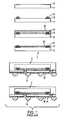
- FIG. 1a cut-away view of a prior art process through which an individual die undergoes bumping and dielectric coating, wherein the assembly is subsequently bonded to a substrate and the conductive bumps break through an adhesive to make electrical contact to the substrate, thereby completing a chip package.
- This preparationdoes not typically extend the physical dimensions of the die in length or width, which has given rise to the term “Chip Scale” for such a preparation.
- Chip Scale PackagesIn an effort to keep up with Moore's Law in Semiconductors, which predicts higher interconnection densities over time, a lot of focus has been spent on Chip Scale Packages to achieve thinner, denser packages and escape routing. Escape routing is the process of interconnecting close proximity die bond pads with mating bond pads in the chip package or the printed circuit board on the applied dielectrics of the CSP.
- the pitch on the diemaybe at 75 microns and the closest pitch obtainable on the printed circuit may be 250 microns.
- the work of providing escape routing through circuitry on the Chip Scale packagebecomes difficult as geometries keep shrinking.
- Chip Scale Packaginghas evolved the technologies of Build-up and Redistribution to assist in this escape routing.
- the state-of-the art in Chip Scale Packagingis the use of multiple layers of metallization and multiple layers of the dielectric to achieve the highest density microelectronic package. This forms a multilayer interconnect and this multilayer process is called Build-up because each dielectric is added sequentially. For formation of more than one metal layer, the process of spinning on a dielectric, forming via holes, metallization and photoimaging is repeated.
- the Build-up processis commonly utilized in the printed circuit and chip packaging manufacturing arenas for multilayer interconnects and is now being used in very dense packages where the Build-up process begins on the surface of the active silicon. These interconnects and packages are sometimes referred to as Wafer Scale Packaging (WSP).
- WSPWafer Scale Packaging
- FIG. 2is a cut-away view of a prior art process through which a multilayer package is prebuilt without a die, wherein an access port is etched in the substrate revealing the connections for the die, the die is placed in the access port, and the structure is bonded together.
- FIG. 3is a cut-away view of a prior art process through which a die is positioned and bonded in an access port of a substrate, wherein the dielectric layers and via interconnects are built on top of this structure.
- FIG. 4is a cut-away view of a prior art build-up on die process utilizing a carrier tape to position the die, wherein the carrier tape is subsequently removed and copper/dielectrics are deposited to form individual layers in a process similar to the Intel Corporation BBUL process.
- This technologyis an extension of Chip Scale Packaging and first locates multiple die on an adhesive tape or similar substrate and molds an encapsulant to secure the die in place.
- Another shortcoming of existing artis that it does not accommodate various component thicknesses during a multilayer structure embedding process because the build-up process requires a very level surface for the first dielectric and metal layers to be successful.
- Various die thicknesseswould be typical in a high speed system because more than one material is used for the wafer processing.
- High Speed systemsmay have multiple die fabricated with two different materials such as Gallium Arsenide (GAAS) and Silicon Germanium (SiGe). Each of these die substrate materials would have with their respective thickness profiles and the thickness difference's would not be suitable for existing build-up on die processes.
- GASGallium Arsenide
- SiGeSilicon Germanium
- Build-up on die and Chip Scale packagingalso have difficulty addressing thermal dissipation requirements of monolithic structures. Multiple die are typically placed in closer proximity to leverage the performance gains associated with such placement. However, as performance increases, the die dissipate more heat energy during operation, and consequently a means of dissipating the heat to an external cooling source either passively by conduction or with an active system becomes more critical.
- Existing build-up on die and CSP technologieshave difficulty in removing excess heat during operation of the system.
- build-up on die and chip scale packagingutilize copper vias with various configurations such as plated-through-holes, blind vias, buried vias, or microvias for interconnecting the die and the copper circuitry in a package.
- These viasconnect one circuitry layer (sometimes referred to as metal layer) to the next.
- These viasare usually formed 90 degrees to the plane of the circuitry, die, or dielectrics.
- a typical designmay take three circuitry layers and three dielectric layers to connect these bond sites utilizing 90 degree vias.
- 90 degree viasexhibit high degrees of stress between the via and the copper circuitry during a thermal excursion due to the CTE mismatch of copper circuitry and the dielectric materials. Cracks often initiate at the interface between the via and copper circuitry which can result in a circuitry failure and an electrical open circuit.
- the present inventionis directed to providing chip to chip optical and electrical interconnection by embedding semiconductor die and other active and passive components in a multilayer interconnect structure such as Microelectromechanical Machines (MEMs) and MEMs Sensors that substantially obviates one or more of the problems due to limitations and disadvantages of the prior art.
- MEMsMicroelectromechanical Machines
- MEMs Sensorsthat substantially obviates one or more of the problems due to limitations and disadvantages of the prior art.
- An object of the present inventionis to develop a means by which entire electronic systems, preferably with multiple active and passive components, can be packaged into one multilayer structure thereby achieving improved performance at high speeds including excellent electrical, mechanical, thermal, cost, and reliability characteristics.
- Another object of the present inventionis to create optical busses or interconnects between adjacent die to achieve a multi-fold improvement in bandwidth for electronic signals in applications such as microprocessor to memory cache bussing, microprocessor to microprocessor data exchange for multi-tasking, or data bussing in high end servers, routers or wireless local-area-networks (WLANS).
- applicationssuch as microprocessor to memory cache bussing, microprocessor to microprocessor data exchange for multi-tasking, or data bussing in high end servers, routers or wireless local-area-networks (WLANS).
- Another object of the present inventionis the creation multi-angled electrical conductive and/or optical vias for improved signal routing between the chips, improved testability of the die during the process, reduction in the amount of required circuitry layers, and improvement in the reduction of stress of the integrated structure during thermal excursions and during operation of the system.
- Another object of the present inventionis to integrate advanced materials to achieve the electrical, mechanical, optical, and thermal properties required of this new structure including nanocomposites, mesocomposites, mesoporous materials, very high Tg (glass transition temperature) organic dielectrics, anisotropic conductive films, copper-invar-copper and other CTE controlled materials which provide low dielectric constants for high speed signal transmission and optical transmission while reducing stress in the finished system.
- Mesocomposites and mesoporous materialsallow optical lasing, detection and wave guiding in addition to allowing formation of optical waveguides with either photo defined, laser, or soft-lithography methods.
- mesocomposites and mesoporous materialshave extremely low dielectric constants, typically on the order of approximately 2.0K, which allows very fast signal transmission speeds in adjacent conductors while maintaining coefficient of thermal expansions in the same order of magnitude of semiconductor substrates (approximately 4-10 ppm/degree Centigrade).
- Very high Tg organic dielectrics300 degrees Celsius provide excellent toughness, elongation properties, and low CTE below the glass transition temperature of the material which provides an excellent dielectric material for build-up on die.
- certain polymershave excellent moisture barrier and moisture uptake properties such as Liquid Crystal Polymers (LCPs) that have excellent properties for integrating and protecting Microelectromechanical Machines (MEMs) components in the build-up process and in the final product.
- LCPsLiquid Crystal Polymers
- MEMsMicroelectromechanical Machines
- the embodiments of the present invention described hereinmake use of a stud bumping process for preparation of die interconnect pads and also two methods of dielectric application to a wafer or singular die: a) spin coating and b) press lamination.
- the stud bumping processhas been demonstrated in die form.
- a typical stud bumping process machineis provided by a model 8098 Large Area Ball Bonder by Kulicke and Soffa.
- Stud bump wireis typically gold wire, although copper, solder, non-lead solder alloys and various other materials may be used without departing from the spirit or the scope of the invention.
- Spin coating and press laminationhave been demonstrated for a 6′′ diameter wafer.
- Typical dielectrics for a build-up process as implemented in the present inventioninclude nanocomposites, mesocomposites, and mesoporous materials such as those provided by SBA Materials, Inc. in Santa Barbara, Calif., also referred to as self-assembled inorganic/block-copolymer composites and mesoporous solids.
- Flexible Circuit materials and adhesivesare preferably similar to Dupont's Pyralux system.
- Very High Tg organic polymersare preferably used, such as Sumitomo's PolyBenzoxazole (PBO) 8000 series, which has a Tg of approximately 300C; Dow Chemical's BenzoCycloButene (BCB), which has a Tg of approximately 300C; HD Microsystems' (Joint venture Dupont/Hitachi) Polyimide (PIQ, PIX tradenames), which has a Tg greater than 300C; or Brewer Science Inc.'s polyimide photoimageable dielectrics.
- Thermally conductive adhesives and films used hereinare preferably similar to Ablefilm 561K.
- Epoxy coated copper as used hereinis preferably similar to Oak-Mitsui Coated Copper.
- Anisotropic conductive films used hereinare preferably of a type similar to ACF from ITO America and a product of the Sony Corporation.
- Embedded passive materials used hereinare preferably similar to high Dk 25 micron film laminates from 3M or Oak-Mitsui.
- Laser Machininghas been and will be utilized in this process using equipment such as, without limitation, the ESI Model 5430 UV Laser Microvia drilling machine.
- Solder sphere placement for interconnectionhas been implemented with equipment such as Shibuya's SolderBall Mounter Model SBM360.
- Sputtering of copper metal for interconnectshas been implemented with equipment such as SFI Metal Depositor Model 8600.
- Microlithographhas been performed with Spectrum 3 Ultratech Steppers.
- FIG. 1a cut-away view of a prior art process through which an individual die undergoes bumping and dielectric coating, wherein the assembly is subsequently bonded to a substrate, and the conductive bumps break through an adhesive to make electrical contact to the substrate, thereby completing a chip package.
- FIG. 2is a cut-away view of a prior art process through which a multilayer package is prebuilt without a die, wherein an access port is etched in the substrate revealing the connections for the die, the die is placed in the access port, and the structure is bonded together.
- FIG. 3is a cut-away view of a prior art process through which a die is positioned and bonded in an access port of a substrate, wherein the dielectric layers and via interconnects are built on top of this structure.
- FIG. 4is a cut-away view of a prior art build-up on die process utilizing a carrier tape to position the die, wherein the carrier tape is subsequently removed and copper/dielectrics are deposited to form individual layers in a process similar to the Intel Corporation BBUL process.
- FIG. 5is a diagram of Build-up on Die with Multi-Angle Stud Bumps and Dielectrics, wherein Vias are constructed by forming channels in a dielectric to accept conductor deposits.
- FIG. 6is a diagram of a build-up process utilizing multi-angle stud bumps and anisotropic conductive film of a first dielectric.
- FIG. 7is a diagram of a build-up process utilizing multi-angle optical vias which accept surface mount optical components.
- FIG. 8is a diagram of a build-up process utilizing multi-angle plated-through hole vias and anisotropic conductive adhesive to interconnect embedded die in a multilayer structure.
- FIG. 9is an optical interconnect build-up structure utilizing embedded VCSEL's multi-angle vias and mesoporous waveguides.
- FIG. 10is a metal core laminate with embedded die and passive components utilizing anisotropic adhesive and multi-angle stud bumps.
- FIG. 11is a multilayer printed circuit board utilizing a copper clad laminate with embedded components from FIG. 10 .
- FIG. 12illustrates preferred Escape Design geometries for Optical and Electrical multi-Angle Vias and Stud Bumping.
- FIG. 13illustrates Wafer Scale Build-up MEMs package with die attach.
- a build-up electrical structurethat is fabricated with a build-up process and multi-angle vias for interconnecting die or multiple die and/or passive components such as capacitors, Microelectromechanical Machines (MEMs), Nanoelectromechanical Machines (MEMs), Bioelectromechanical Machines (BioMEMs), sensors, planar capacitors, resistors, planar resistors, inductors, fuel cells, antennas, thin film batteries, VCSEL's, photodiodes, or other active and passive components is described herein.
- Typical preferred process times and temperaturesare 350° C. for one hour with normal prepregs, 250° C. for 90 seconds with mesoporous materials and 350° C. for 20 seconds for anistropic conductive adhesives.
- Typical process temperatures for very high Tg photo-imageable dielectricswould be 375° C. for 1 hour.
- Via formationsare preferably made with laser milling with an ultraviolet or carbon dioxide laser, although via formations can be made using a photolithography process followed by developing and/or chemical milling, or with soft lithography.
- Stud Bumpingpreferably utilizes gold wire and is performed with a stud bumping machine such as the K&S 300 mm stud bumping machine.
- Chip placementis preferably performed with standard chip placement robotics with placement accuracies to 0.5 micron.
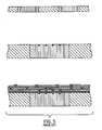
- FIG. 5illustrates a build-up on die with multi-Angle Via Process and structure.
- Die or other active componentssuch as MEMs 500 are tack-bonded into a multi-depth cavity 515 using a thermally conductive adhesive film 505 with a die bonding and placement machine.
- Multi-angle stud bumps 520are placed on the active sites of the die and/or components in each of the active sites requiring interconnection.
- a controlled CTE dielectric 530such as a mesoporous material or a very high Tg photo-imageable dielectric, is deposited over the die or multiple die utilizing a spin coating or lamination process thereby sandwiching and embedding the die.
- An optical waveguideis formed with the nanocomposites or nanoporous materials if required for chip to chip optical interconnects 535 and a dielectric channel 540 is formed to expose the stud bumping through soft lithography, photolithography or laser trenching.
- Copper plating 550is deposited on the surface and in the channels utilizing either wet chemistry plating or sputtering.
- copper circuitry 560is preferably etched in the copper plating utilizing photolithography and chemical milling, thereby forming a first circuitry (first metal) layer.
- Solder Mask 580 and solder balls 570are placed on the structure surface utilizing sphere drop equipment to complete the interconnect and to allow attachment to other interconnects.
- the multi-depth cavitiesaccommodate different die thicknesses and the multi-angle vias allow for escape routing from the die to other components.
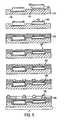
- FIG. 6illustrates a Build-up process using anisotropic adhesive with multi-angle vias.
- a thermally conductive adhesive pad 610is placed on heatsink 600 , which is preferably made of copper.
- Die or bare components such as MEMs 620are accurately positioned on the thermal adhesive and the components are preferably stud bumped utilizing a stud bumping process with multi-angle vias 630 .
- Copper foil 640is laminated onto this structure with anisotropic conductive adhesive 650 utilizing lamination equipment, thereby embedding the die within the structure.
- the anisotropic adhesiveallows conductivity to occur only in the vertical plane.
- the copperis etched into circuitry as in FIG.
- solder balls 660 and solder mask 670are placed on the circuitry utilizing sphere drop equipment and solder mask screening process equipment to complete the structure where connection between the multiangle vias and the copper circuitry is performed by the anisotropic conductive adhesive.
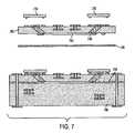
- FIG. 7illustrates another embodiment of the present invention.
- a flex circuit substructure 700with multi-angle vias 740 , is fabricated with an optical waveguide of mesocomposite material 730 applied to the bottom side of the flex circuit substructure and positioned between the optical vias of the substructure.
- the multiangle viasallow light to transmit by reflection through the optical via.
- This structureforms an optical pathway from a VCSEL laser light source 710 on the surface to a photodiode 720 , also on the surface with the light pathway following the multi-angle vias on either side of the optical waveguide.
- This flex circuitis then attached to a backplane multilayer 750 utilizing an adhesive film 745 with a lamination process and a plated-through hole process, thereby completing the optical and electrical interconnect.
- FIG. 8illustrates an electrical version of FIG. 7 with embedded die.
- a flex circuit 800 with multi-angle electrical vias 820is laminated to a multilayer substrate 850 with anisotropic conductive adhesive 830 .
- a completed multilayer substrate 860is produced by finishing the structure with a standard printed circuit process to achieve plated-through holes. Electrical interconnection between components and die is accomplished through the anisotropic conductive adhesive and the multi-angle stud bumping and electrical vias.
- FIG. 9is another embodiment of the present invention.
- active optical componentsincluding VSCEL 900 and Photodiode 910
- VSCEL 900 and Photodiode 910are tack bonded with a short time and temperature anisotropic conductive adhesive to a build-up on die composite 930 .
- a two-sided microflex with multi-angle vias 940is laminated to the structure utilizing a second ply of anistropic adhesive 920 .
- a mesoporous or mesocomposite waveguide 960is formed between the multi-angle optical vias to form a complete chip to chip light path through the optical vias and the optical waveguide.
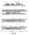
- FIG. 10is a preferred embodiment of the present invention in which a copper clad laminate structure is constructed with a build-up process and incorporates embedded die and active/passive components in the copper clad laminate. This structure can later be relaminated into another multilayer structure or printed circuit. Die 1010 and passive component or MEMs device 1030 with multi-angle stud bumps are accurately placed and tack bonded on epoxy coated copper foil 1020 .
- Composite 1060is formed utilizing a combination of prepreg 1040 , anisotropic conductive adhesive 1050 and epoxy coated copper foil 1020 . Subsequently, composite 1060 is etched with a normal printed circuit process to form an inner circuit layer for a multilayer system 1070 with embedded components.
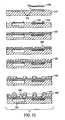
- FIG. 11illustrates a multilayer printed circuit and interconnect utilizing the multilayer core from FIG. 10 with embedded die and/or components.
- the inner core layer 1120is laminated with prepreg adhesive 1110 and copper foil 1100 in a lamination press.
- the structureis then processed with normal printed circuit processing to form blind vias 1130 and through hole vias 1140 .
- FIG. 12illustrates preferred geometries for multi-angle vias 1200 and for stud bumps 1210 .
- Preferred geometrical relationships between two different planes and their respective pitchesare shown in ISO view 1220 , top view 1230 and side view 1240 .
- the two pitch planesrepresent the tighter semiconductor die pitch plane 1250 and a wider pitch plane 1260 typical of printed circuits. These relationships can be used to determine the correct via angle, either electrically or optically, and the subsequent thickness necessary to achieve the angle for escape routing between the different planes of reference.
- FIG. 13illustrates a build-up on wafer with a multi-Angle Via Process and structure.
- Die or other active components 1300are preferably tack-bonded into a multi-depth cavity 1315 using a thermally conductive adhesive film 1305 with a die bonding and placement machine.
- Multi-angle stud bumps 1320are preferably placed on the active sites of the die and on the active MEMs devices which are integral to the wafer substrate 1310 .
- An alternative to the stud-bumpingis apply standard under bump metallization (UBM) as an interconnect interface.
- UBMunder bump metallization
- a controlled CTE dielectric 1330such as a mesoporous material or a very high Tg photo-imageable dielectric, is deposited over the wafer substrate utilizing a spin coating or lamination process thereby sandwiching and embedding the die.
- a dielectric channel 1340is formed to expose the stud bumping through soft lithography, photolithography or laser trenching.
- Copper plating 1350is deposited on the surface and in the channels utilizing either wet chemistry plating or sputtering.
- copper circuitry 1360is preferably etched in the copper plating utilizing photolithography and chemical milling, thereby forming a first circuitry (first metal) layer.
- Solder Mask 1380 and solder balls 1370are preferably placed on the structure surface utilizing sphere drop equipment to complete the interconnect and to allow attachment to other interconnects.
- Aperture Vias 1390are preferably formed through either the wafer substrate or through the top dielectrics by laser micromachining, chemical etching or through reactive ion etching to expose the active Microelectromechanical Machine (MEMs) active surfaces.
- MEMsMicroelectromechanical Machine
- the multi-depth cavitiescan accommodate different die thicknesses and the multi-angle vias allow for escape routing from the die to other components.
Landscapes
- Engineering & Computer Science (AREA)
- Microelectronics & Electronic Packaging (AREA)
- Computer Hardware Design (AREA)
- Power Engineering (AREA)
- Physics & Mathematics (AREA)
- Manufacturing & Machinery (AREA)
- General Physics & Mathematics (AREA)
- Condensed Matter Physics & Semiconductors (AREA)
- Optics & Photonics (AREA)
- Production Of Multi-Layered Print Wiring Board (AREA)
- Micromachines (AREA)
Abstract
Description
- The present invention is related to, and claims priority from, Provisional U.S. Patent Application Ser. No. 60/424,710, the teachings of which are incorporated herein by reference in their entirety.
- The present invention relates to the field of high density and high speed semiconductor packages and optical interconnects. In particular, the present invention provides build-up structures for interconnecting single or multiple semiconductor chips, Microelectromechanical Machines (MEMs) and/or die thereof of various thicknesses embedded in multilayer structures, a System-In-Package, Wafer-Scale Packages, or metal clad laminates utilizing multi-angle optical and/or electrical vias and controlled CTE dielectrics such as mesocomposites, to achieve electrical and optical performance.
- In the manufacturing of chip packaging, attempts have been made to maintain efficient interconnection between the die and other components as die and pad densities increase at a dramatic rate and geometries decrease at an equally dramatic rate. The technology roadmap for semiconductor packaging has technical drivers which describe meticulous efforts to bring the die closer to other components through thinner and denser chip packaging to achieve higher finished system functionality. In one such effort, a semiconductor package is sometimes eliminated and the die are placed directly on the printed circuit in a flip-chip process which often uses die that have been prepared for placement through a process known as “Chip Scale Packaging” or CSP.
- Chip Scale Packaging involves preparing a semiconductor die with appropriate dielectrics and conductive bumps on the active site of the die so that the die is properly prepared to attach to another interconnect such as a printed circuit board.
FIG. 1 a cut-away view of a prior art process through which an individual die undergoes bumping and dielectric coating, wherein the assembly is subsequently bonded to a substrate and the conductive bumps break through an adhesive to make electrical contact to the substrate, thereby completing a chip package. This preparation does not typically extend the physical dimensions of the die in length or width, which has given rise to the term “Chip Scale” for such a preparation. - In an effort to keep up with Moore's Law in Semiconductors, which predicts higher interconnection densities over time, a lot of focus has been spent on Chip Scale Packages to achieve thinner, denser packages and escape routing. Escape routing is the process of interconnecting close proximity die bond pads with mating bond pads in the chip package or the printed circuit board on the applied dielectrics of the CSP. The pitch on the die maybe at 75 microns and the closest pitch obtainable on the printed circuit may be 250 microns. The work of providing escape routing through circuitry on the Chip Scale package becomes difficult as geometries keep shrinking. Chip Scale Packaging has evolved the technologies of Build-up and Redistribution to assist in this escape routing.
- Build-up processes and Redistribution technology places dielectrics external to the active wafer or die surface for the Chip Scale Package, usually through a spin coating process in the wafer fab, followed by formation of holes in the dielectric usually through a photoimaging process. The wafer and dielectric then proceeds through a metallic sputtering process to apply a conductor to achieve interconnect vias through the holes in the dielectric and conductive material on the surface. The surface metal is then chemically milled to a circuitry pattern utilizing another photoimaging process thereby completing the external circuitry for a first metal layer on the wafer or die for the Chip Scale Package. After this process the wafer is sawed to release the Chip Scale Package which includes a singulated die.
- The state-of-the art in Chip Scale Packaging is the use of multiple layers of metallization and multiple layers of the dielectric to achieve the highest density microelectronic package. This forms a multilayer interconnect and this multilayer process is called Build-up because each dielectric is added sequentially. For formation of more than one metal layer, the process of spinning on a dielectric, forming via holes, metallization and photoimaging is repeated. The Build-up process is commonly utilized in the printed circuit and chip packaging manufacturing arenas for multilayer interconnects and is now being used in very dense packages where the Build-up process begins on the surface of the active silicon. These interconnects and packages are sometimes referred to as Wafer Scale Packaging (WSP).
FIG. 2 is a cut-away view of a prior art process through which a multilayer package is prebuilt without a die, wherein an access port is etched in the substrate revealing the connections for the die, the die is placed in the access port, and the structure is bonded together.FIG. 3 is a cut-away view of a prior art process through which a die is positioned and bonded in an access port of a substrate, wherein the dielectric layers and via interconnects are built on top of this structure. - Another multiple die version of Chip Scale Packaging is sometimes referred to as build-up on die or System-In-Package (SIP). Intel Corporation developed a version of build-up on die referred to as BBUL.
FIG. 4 is a cut-away view of a prior art build-up on die process utilizing a carrier tape to position the die, wherein the carrier tape is subsequently removed and copper/dielectrics are deposited to form individual layers in a process similar to the Intel Corporation BBUL process. This technology is an extension of Chip Scale Packaging and first locates multiple die on an adhesive tape or similar substrate and molds an encapsulant to secure the die in place. After removing the adhesive tape, a series of dielectrics and conductive layers are built upon these initial die thereby forming the chip to chip interconnect structure. There are benefits to the build-up on die process over typical chip packaging because of the close proximity that is possible with the die and the interconnections. This closer proximity provides improved electrical performance due to lower inductance of the vias and improved signal integrity because signals from die to die travel a shorter distance. - Complex build-up on die processing suffers from technological constraints due to reliability and quality issues when temperature excursions (as in soldering) cause fractures in the composite which are due to Coefficient of Thermal Expansion (CTE) differences between the various materials and components of the package. These issues are even more problematic when attempts are made to package multiple die of different geometries and materials in a monolithic structure. For example, encapsulation materials of the embedded die and the design of the vias often result in an undesirably rigid structure which, combined with the CTE mismatch materials, causes delamination (adhesion failure) during a thermal stress or soldering operation. Furthermore, the embedding of various components, such as sensors, MEMs (Micro Electromechnaical Machines), capacitors, resistors, inductors, transducers and antennas, each of which typically has a unique CTE, cannot be performed in multicomponent structures due to additional stress issues of the various materials and their different CTE values.
- Another shortcoming of existing art is that it does not accommodate various component thicknesses during a multilayer structure embedding process because the build-up process requires a very level surface for the first dielectric and metal layers to be successful. Various die thicknesses would be typical in a high speed system because more than one material is used for the wafer processing. High Speed systems may have multiple die fabricated with two different materials such as Gallium Arsenide (GAAS) and Silicon Germanium (SiGe). Each of these die substrate materials would have with their respective thickness profiles and the thickness difference's would not be suitable for existing build-up on die processes.
- Still another shortcoming of build-up on die prior art is that it does not facilitate die electrical testing prior to embedding. Semiconductor wafer processing techniques are known to have defects that are undetectable unless tested, and testing often occurs after the die is packaged. In a build-up on die process, if a die is defective, the entire monolithic structure will be wasted because testing cannot be performed very early in the process. Only known good die (KGD) can be used with prior art build-up on die processes.
- Build-up on Die and Chip Scale packaging do not accommodate optical transmission of data between chips in either discrete component technologies or in monolithic technologies. As digital broadband increases its bandwidth and microprocessor speeds increase, there are technology drivers to utilize optical waveguides, embedded optical components and solid state monolithic structures for die-to-die, or die-to-component interconnect structures. The bandwidth limit for copper transmission of digital signals, for example, is between 600 Megabits/second and 10 Gigabits/second depending on the circuit design and the absorbance of the dielectric materials. Optical signal transmission can increase available bandwidth to several times copper wire bandwidth. Existing build-up on die techniques do not accommodate the direct connection of optical components for die-to-die or component-to-component optical interconnections to tap into these higher bandwidths.
- Build-up on die and Chip Scale packaging also have difficulty addressing thermal dissipation requirements of monolithic structures. Multiple die are typically placed in closer proximity to leverage the performance gains associated with such placement. However, as performance increases, the die dissipate more heat energy during operation, and consequently a means of dissipating the heat to an external cooling source either passively by conduction or with an active system becomes more critical. Existing build-up on die and CSP technologies have difficulty in removing excess heat during operation of the system.
- Typically, build-up on die and chip scale packaging utilize copper vias with various configurations such as plated-through-holes, blind vias, buried vias, or microvias for interconnecting the die and the copper circuitry in a package. These vias connect one circuitry layer (sometimes referred to as metal layer) to the next. These vias are usually formed 90 degrees to the plane of the circuitry, die, or dielectrics.
- Although commonly used, sharp, 90 degree structures have several disadvantages when utilized unilaterally throughout a structure in high speed, high density designs. Both electrical signals and optical signals experience significant signal loss at a 90 degree bend. Electrical signals radiate significant amounts of energy and noise at the 90 degree bend thereby degrading the signal. Optical signals experience a more difficult hurdle because a relatively large percentage of the incoming optical light is reflected back to the source, never making the bend. Also, 90 degree angles are sometimes not the optimum escape design routing from the very tight pitch on the die to wider pitched components on other components. For example, a die could have a 75 micron pitch or distance between bonding pads. A printed circuit board may have a 250 micron pitch. A typical design may take three circuitry layers and three dielectric layers to connect these bond sites utilizing 90 degree vias. As the mismatch between the pitch of the die and the component increases, the likelihood of requiring more circuitry layers increases with 90 degree vias, thereby increasing the cost of the system. In addition, 90 degree vias exhibit high degrees of stress between the via and the copper circuitry during a thermal excursion due to the CTE mismatch of copper circuitry and the dielectric materials. Cracks often initiate at the interface between the via and copper circuitry which can result in a circuitry failure and an electrical open circuit.
- Accordingly, the present invention is directed to providing chip to chip optical and electrical interconnection by embedding semiconductor die and other active and passive components in a multilayer interconnect structure such as Microelectromechanical Machines (MEMs) and MEMs Sensors that substantially obviates one or more of the problems due to limitations and disadvantages of the prior art.
- An object of the present invention is to develop a means by which entire electronic systems, preferably with multiple active and passive components, can be packaged into one multilayer structure thereby achieving improved performance at high speeds including excellent electrical, mechanical, thermal, cost, and reliability characteristics.
- Another object of the present invention is to create optical busses or interconnects between adjacent die to achieve a multi-fold improvement in bandwidth for electronic signals in applications such as microprocessor to memory cache bussing, microprocessor to microprocessor data exchange for multi-tasking, or data bussing in high end servers, routers or wireless local-area-networks (WLANS).
- Another object of the present invention is the creation multi-angled electrical conductive and/or optical vias for improved signal routing between the chips, improved testability of the die during the process, reduction in the amount of required circuitry layers, and improvement in the reduction of stress of the integrated structure during thermal excursions and during operation of the system.
- Another object of the present invention is to integrate advanced materials to achieve the electrical, mechanical, optical, and thermal properties required of this new structure including nanocomposites, mesocomposites, mesoporous materials, very high Tg (glass transition temperature) organic dielectrics, anisotropic conductive films, copper-invar-copper and other CTE controlled materials which provide low dielectric constants for high speed signal transmission and optical transmission while reducing stress in the finished system. Mesocomposites and mesoporous materials allow optical lasing, detection and wave guiding in addition to allowing formation of optical waveguides with either photo defined, laser, or soft-lithography methods. Also mesocomposites and mesoporous materials have extremely low dielectric constants, typically on the order of approximately 2.0K, which allows very fast signal transmission speeds in adjacent conductors while maintaining coefficient of thermal expansions in the same order of magnitude of semiconductor substrates (approximately 4-10 ppm/degree Centigrade). Very high Tg organic dielectrics (300 degrees Celsius) provide excellent toughness, elongation properties, and low CTE below the glass transition temperature of the material which provides an excellent dielectric material for build-up on die. Furthermore, certain polymers have excellent moisture barrier and moisture uptake properties such as Liquid Crystal Polymers (LCPs) that have excellent properties for integrating and protecting Microelectromechanical Machines (MEMs) components in the build-up process and in the final product.
- Additional features and advantages of the invention will be set forth in the description which follows, and in part will be apparent from the description or may be learned by practice of the invention. The objectives and other advantages of the invention will be realized and attained by the structure particularly pointed out in the written description hereof and the appended drawings.
- The embodiments of the present invention described herein make use of a stud bumping process for preparation of die interconnect pads and also two methods of dielectric application to a wafer or singular die: a) spin coating and b) press lamination. The stud bumping process has been demonstrated in die form. A typical stud bumping process machine is provided by a model 8098 Large Area Ball Bonder by Kulicke and Soffa. Stud bump wire is typically gold wire, although copper, solder, non-lead solder alloys and various other materials may be used without departing from the spirit or the scope of the invention. Spin coating and press lamination have been demonstrated for a 6″ diameter wafer. Typical dielectrics for a build-up process as implemented in the present invention include nanocomposites, mesocomposites, and mesoporous materials such as those provided by SBA Materials, Inc. in Santa Barbara, Calif., also referred to as self-assembled inorganic/block-copolymer composites and mesoporous solids. Flexible Circuit materials and adhesives are preferably similar to Dupont's Pyralux system. Very High Tg organic polymers are preferably used, such as Sumitomo's PolyBenzoxazole (PBO) 8000 series, which has a Tg of approximately 300C; Dow Chemical's BenzoCycloButene (BCB), which has a Tg of approximately 300C; HD Microsystems' (Joint venture Dupont/Hitachi) Polyimide (PIQ, PIX tradenames), which has a Tg greater than 300C; or Brewer Science Inc.'s polyimide photoimageable dielectrics. Thermally conductive adhesives and films used herein are preferably similar to Ablefilm 561K. Epoxy coated copper as used herein is preferably similar to Oak-Mitsui Coated Copper. Anisotropic conductive films used herein are preferably of a type similar to ACF from ITO America and a product of the Sony Corporation. Embedded passive materials used herein are preferably similar to high Dk 25 micron film laminates from 3M or Oak-Mitsui. Laser Machining has been and will be utilized in this process using equipment such as, without limitation, the ESI Model 5430 UV Laser Microvia drilling machine. Solder sphere placement for interconnection has been implemented with equipment such as Shibuya's SolderBall Mounter Model SBM360. Sputtering of copper metal for interconnects has been implemented with equipment such as SFI Metal Depositor Model 8600. Microlithograph has been performed with
Spectrum 3 Ultratech Steppers. Dielectric Placement has been performed with spin coaters such as Karl Suss Model ACS-200 and anisotropic film bonders similar to those distributed by Ito America. The above-referenced materials and equipment are included herein as exemplary of those used in a preferred embodiment of the present invention, and should not be interpreted as limiting the scope of the invention thereto. It should be apparent to one skilled in the art that alternative materials and equipment may be substituted therefor without departing from the spirit or the scope of the invention. - It is to be understood that both the foregoing general description and the following detailed description are exemplary and explanatory and are intended to provide further explanation of the invention as claimed.
- The accompanying drawings, which are included to provide a further understanding of the invention and are incorporated in and constitute a part of this specification, illustrate embodiments of the invention and together with the description serve to explain the principles of the invention.
- In the drawings:
FIG. 1 a cut-away view of a prior art process through which an individual die undergoes bumping and dielectric coating, wherein the assembly is subsequently bonded to a substrate, and the conductive bumps break through an adhesive to make electrical contact to the substrate, thereby completing a chip package.FIG. 2 is a cut-away view of a prior art process through which a multilayer package is prebuilt without a die, wherein an access port is etched in the substrate revealing the connections for the die, the die is placed in the access port, and the structure is bonded together.FIG. 3 is a cut-away view of a prior art process through which a die is positioned and bonded in an access port of a substrate, wherein the dielectric layers and via interconnects are built on top of this structure.FIG. 4 is a cut-away view of a prior art build-up on die process utilizing a carrier tape to position the die, wherein the carrier tape is subsequently removed and copper/dielectrics are deposited to form individual layers in a process similar to the Intel Corporation BBUL process.FIG. 5 is a diagram of Build-up on Die with Multi-Angle Stud Bumps and Dielectrics, wherein Vias are constructed by forming channels in a dielectric to accept conductor deposits.FIG. 6 is a diagram of a build-up process utilizing multi-angle stud bumps and anisotropic conductive film of a first dielectric.FIG. 7 is a diagram of a build-up process utilizing multi-angle optical vias which accept surface mount optical components.FIG. 8 is a diagram of a build-up process utilizing multi-angle plated-through hole vias and anisotropic conductive adhesive to interconnect embedded die in a multilayer structure.FIG. 9 is an optical interconnect build-up structure utilizing embedded VCSEL's multi-angle vias and mesoporous waveguides.FIG. 10 is a metal core laminate with embedded die and passive components utilizing anisotropic adhesive and multi-angle stud bumps.FIG. 11 is a multilayer printed circuit board utilizing a copper clad laminate with embedded components fromFIG. 10 .FIG. 12 illustrates preferred Escape Design geometries for Optical and Electrical multi-Angle Vias and Stud Bumping.FIG. 13 illustrates Wafer Scale Build-up MEMs package with die attach.- Reference will now be made in detail to preferred embodiments of the present invention, examples of which are illustrated in the accompanying drawings.
- A build-up electrical structure that is fabricated with a build-up process and multi-angle vias for interconnecting die or multiple die and/or passive components such as capacitors, Microelectromechanical Machines (MEMs), Nanoelectromechanical Machines (MEMs), Bioelectromechanical Machines (BioMEMs), sensors, planar capacitors, resistors, planar resistors, inductors, fuel cells, antennas, thin film batteries, VCSEL's, photodiodes, or other active and passive components is described herein. Typical preferred process times and temperatures are 350° C. for one hour with normal prepregs, 250° C. for 90 seconds with mesoporous materials and 350° C. for 20 seconds for anistropic conductive adhesives. Typical process temperatures for very high Tg photo-imageable dielectrics would be 375° C. for 1 hour. Via formations are preferably made with laser milling with an ultraviolet or carbon dioxide laser, although via formations can be made using a photolithography process followed by developing and/or chemical milling, or with soft lithography. Stud Bumping preferably utilizes gold wire and is performed with a stud bumping machine such as the K&S 300 mm stud bumping machine. Chip placement is preferably performed with standard chip placement robotics with placement accuracies to 0.5 micron. The above-referenced process times, temperatures, and equipment are included herein as exemplary of those used in a preferred embodiment of the present invention, and should not be interpreted as limiting the scope of the invention thereto. It should be apparent to one skilled in the art that alternative process times, temperatures, and equipment may be substituted therefor without departing from the spirit or the scope of the invention.
FIG. 5 illustrates a build-up on die with multi-Angle Via Process and structure. Die or other active components such asMEMs 500 are tack-bonded into amulti-depth cavity 515 using a thermally conductiveadhesive film 505 with a die bonding and placement machine. Multi-angle stud bumps520 are placed on the active sites of the die and/or components in each of the active sites requiring interconnection. A controlledCTE dielectric 530, such as a mesoporous material or a very high Tg photo-imageable dielectric, is deposited over the die or multiple die utilizing a spin coating or lamination process thereby sandwiching and embedding the die. An optical waveguide is formed with the nanocomposites or nanoporous materials if required for chip to chip optical interconnects535 and adielectric channel 540 is formed to expose the stud bumping through soft lithography, photolithography or laser trenching. Copper plating550 is deposited on the surface and in the channels utilizing either wet chemistry plating or sputtering. In a subsequent step,copper circuitry 560 is preferably etched in the copper plating utilizing photolithography and chemical milling, thereby forming a first circuitry (first metal) layer.Solder Mask 580 andsolder balls 570 are placed on the structure surface utilizing sphere drop equipment to complete the interconnect and to allow attachment to other interconnects. The multi-depth cavities accommodate different die thicknesses and the multi-angle vias allow for escape routing from the die to other components.FIG. 6 illustrates a Build-up process using anisotropic adhesive with multi-angle vias. In a process similar to that illustrated inFIG. 5 , a thermally conductiveadhesive pad 610 is placed on heatsink600, which is preferably made of copper. Die or bare components such asMEMs 620 are accurately positioned on the thermal adhesive and the components are preferably stud bumped utilizing a stud bumping process withmulti-angle vias 630.Copper foil 640 is laminated onto this structure with anisotropic conductive adhesive650 utilizing lamination equipment, thereby embedding the die within the structure. The anisotropic adhesive allows conductivity to occur only in the vertical plane. The copper is etched into circuitry as inFIG. 5 utilizing normal printed circuit processing, such as photolithography and chemical milling.Solder balls 660 andsolder mask 670 are placed on the circuitry utilizing sphere drop equipment and solder mask screening process equipment to complete the structure where connection between the multiangle vias and the copper circuitry is performed by the anisotropic conductive adhesive.FIG. 7 illustrates another embodiment of the present invention. In this embodiment, aflex circuit substructure 700, withmulti-angle vias 740, is fabricated with an optical waveguide ofmesocomposite material 730 applied to the bottom side of the flex circuit substructure and positioned between the optical vias of the substructure. The multiangle vias allow light to transmit by reflection through the optical via. This structure forms an optical pathway from a VCSELlaser light source 710 on the surface to aphotodiode 720, also on the surface with the light pathway following the multi-angle vias on either side of the optical waveguide. This flex circuit is then attached to abackplane multilayer 750 utilizing anadhesive film 745 with a lamination process and a plated-through hole process, thereby completing the optical and electrical interconnect.FIG. 8 illustrates an electrical version ofFIG. 7 with embedded die. Aflex circuit 800 with multi-angleelectrical vias 820 is laminated to amultilayer substrate 850 with anisotropicconductive adhesive 830. A completedmultilayer substrate 860 is produced by finishing the structure with a standard printed circuit process to achieve plated-through holes. Electrical interconnection between components and die is accomplished through the anisotropic conductive adhesive and the multi-angle stud bumping and electrical vias.FIG. 9 is another embodiment of the present invention. In this embodiment, active optical components, includingVSCEL 900 andPhotodiode 910, are tack bonded with a short time and temperature anisotropic conductive adhesive to a build-up ondie composite 930. Subsequently, a two-sided microflex withmulti-angle vias 940 is laminated to the structure utilizing a second ply ofanistropic adhesive 920. After lamination a mesoporous ormesocomposite waveguide 960 is formed between the multi-angle optical vias to form a complete chip to chip light path through the optical vias and the optical waveguide.FIG. 10 is a preferred embodiment of the present invention in which a copper clad laminate structure is constructed with a build-up process and incorporates embedded die and active/passive components in the copper clad laminate. This structure can later be relaminated into another multilayer structure or printed circuit.Die 1010 and passive component orMEMs device 1030 with multi-angle stud bumps are accurately placed and tack bonded on epoxy coatedcopper foil 1020.Composite 1060 is formed utilizing a combination ofprepreg 1040, anisotropic conductive adhesive1050 and epoxy coatedcopper foil 1020. Subsequently, composite1060 is etched with a normal printed circuit process to form an inner circuit layer for amultilayer system 1070 with embedded components.FIG. 11 illustrates a multilayer printed circuit and interconnect utilizing the multilayer core fromFIG. 10 with embedded die and/or components. Theinner core layer 1120 is laminated with prepreg adhesive1110 andcopper foil 1100 in a lamination press. The structure is then processed with normal printed circuit processing to formblind vias 1130 and throughhole vias 1140.FIG. 12 illustrates preferred geometries formulti-angle vias 1200 and for stud bumps1210. Preferred geometrical relationships between two different planes and their respective pitches are shown inISO view 1220,top view 1230 andside view 1240. The two pitch planes represent the tighter semiconductor diepitch plane 1250 and awider pitch plane 1260 typical of printed circuits. These relationships can be used to determine the correct via angle, either electrically or optically, and the subsequent thickness necessary to achieve the angle for escape routing between the different planes of reference.FIG. 13 illustrates a build-up on wafer with a multi-Angle Via Process and structure. Die or otheractive components 1300 are preferably tack-bonded into amulti-depth cavity 1315 using a thermally conductiveadhesive film 1305 with a die bonding and placement machine. Multi-angle stud bumps1320 are preferably placed on the active sites of the die and on the active MEMs devices which are integral to the wafer substrate1310. An alternative to the stud-bumping is apply standard under bump metallization (UBM) as an interconnect interface. A controlledCTE dielectric 1330, such as a mesoporous material or a very high Tg photo-imageable dielectric, is deposited over the wafer substrate utilizing a spin coating or lamination process thereby sandwiching and embedding the die. Adielectric channel 1340 is formed to expose the stud bumping through soft lithography, photolithography or laser trenching. Copper plating1350 is deposited on the surface and in the channels utilizing either wet chemistry plating or sputtering. In a subsequent step,copper circuitry 1360 is preferably etched in the copper plating utilizing photolithography and chemical milling, thereby forming a first circuitry (first metal) layer.Solder Mask 1380 andsolder balls 1370 are preferably placed on the structure surface utilizing sphere drop equipment to complete the interconnect and to allow attachment to other interconnects.Aperture Vias 1390 are preferably formed through either the wafer substrate or through the top dielectrics by laser micromachining, chemical etching or through reactive ion etching to expose the active Microelectromechanical Machine (MEMs) active surfaces. The multi-depth cavities can accommodate different die thicknesses and the multi-angle vias allow for escape routing from the die to other components.- While the invention has been described in detail and with reference to specific embodiments thereof, it will be apparent to those skilled in the art that various changes and modifications can be made therein without departing from the spirit and scope thereof. Thus, it is intended that the present invention cover the modifications and variations of this invention provided they come within the scope of the appended claims and their equivalents.
Claims (43)
Priority Applications (2)
| Application Number | Priority Date | Filing Date | Title |
|---|---|---|---|
| US10/704,131US6919508B2 (en) | 2002-11-08 | 2003-11-10 | Build-up structures with multi-angle vias for chip to chip interconnects and optical bussing |
| US11/145,948US7011988B2 (en) | 2002-11-08 | 2005-06-07 | Build-up structures with multi-angle vias for Chip to Chip interconnects and optical bussing |
Applications Claiming Priority (2)
| Application Number | Priority Date | Filing Date | Title |
|---|---|---|---|
| US42471002P | 2002-11-08 | 2002-11-08 | |
| US10/704,131US6919508B2 (en) | 2002-11-08 | 2003-11-10 | Build-up structures with multi-angle vias for chip to chip interconnects and optical bussing |
Related Child Applications (1)
| Application Number | Title | Priority Date | Filing Date |
|---|---|---|---|
| US11/145,948ContinuationUS7011988B2 (en) | 2002-11-08 | 2005-06-07 | Build-up structures with multi-angle vias for Chip to Chip interconnects and optical bussing |
Publications (2)
| Publication Number | Publication Date |
|---|---|
| US20050087356A1true US20050087356A1 (en) | 2005-04-28 |
| US6919508B2 US6919508B2 (en) | 2005-07-19 |
Family
ID=34526080
Family Applications (2)
| Application Number | Title | Priority Date | Filing Date |
|---|---|---|---|
| US10/704,131Expired - Fee RelatedUS6919508B2 (en) | 2002-11-08 | 2003-11-10 | Build-up structures with multi-angle vias for chip to chip interconnects and optical bussing |
| US11/145,948Expired - Fee RelatedUS7011988B2 (en) | 2002-11-08 | 2005-06-07 | Build-up structures with multi-angle vias for Chip to Chip interconnects and optical bussing |
Family Applications After (1)
| Application Number | Title | Priority Date | Filing Date |
|---|---|---|---|
| US11/145,948Expired - Fee RelatedUS7011988B2 (en) | 2002-11-08 | 2005-06-07 | Build-up structures with multi-angle vias for Chip to Chip interconnects and optical bussing |
Country Status (1)
| Country | Link |
|---|---|
| US (2) | US6919508B2 (en) |
Cited By (38)
| Publication number | Priority date | Publication date | Assignee | Title |
|---|---|---|---|---|
| US20030222282A1 (en)* | 2002-04-29 | 2003-12-04 | Fjelstad Joseph C. | Direct-connect signaling system |
| US20050285266A1 (en)* | 2004-06-18 | 2005-12-29 | Martin Reiss | Arrangement for increasing the reliability of substrate-based BGA packages |
| US20060005384A1 (en)* | 2004-07-06 | 2006-01-12 | Advanced Semiconductor Engineering, Inc. | Manufacturing method of a multi-layer circuit board with an embedded passive component |
| DE102006005340A1 (en)* | 2006-02-07 | 2007-08-09 | Volkswagen Ag | Detecting device for operational data of fuel cell in fuel cell stack, has sensor plate integrated into fuel cell stack |
| JP2007260866A (en)* | 2006-03-29 | 2007-10-11 | Toshiba Corp | Semiconductor device and manufacturing method thereof |
| WO2009017271A3 (en)* | 2007-07-31 | 2009-09-24 | Wavenics, Inc | Metal-based package substrate, three-dimensional multi-layered package module using the same, and manufacturing method thereof |
| US7750446B2 (en) | 2002-04-29 | 2010-07-06 | Interconnect Portfolio Llc | IC package structures having separate circuit interconnection structures and assemblies constructed thereof |
| US20110057273A1 (en)* | 2009-09-04 | 2011-03-10 | Analog Devices, Inc. | System with Recessed Sensing or Processing Elements |
| US20110073357A1 (en)* | 2008-06-02 | 2011-03-31 | Nxp B.V. | Electronic device and method of manufacturing an electronic device |
| US20110298101A1 (en)* | 2010-06-02 | 2011-12-08 | Stats Chippac, Ltd. | Semiconductor Device and Method of Forming EMI Shielding Layer with Conductive Material Around Semiconductor Die |
| US20120104517A1 (en)* | 2010-11-01 | 2012-05-03 | Siliconware Precision Industries Co., Ltd. | Package structure with micro-electromechanical element and manufacturing method thereof |
| US20130301228A1 (en)* | 2011-01-30 | 2013-11-14 | Nantong Fujitsu Microelectronics Co., Ltd. | Packaging structure |
| CN104321865A (en)* | 2012-06-29 | 2015-01-28 | 英特尔公司 | Semiconductor package with mechanical fuse |
| WO2015038250A1 (en)* | 2013-09-11 | 2015-03-19 | Harris Corporation | Embedded electronic packaging and associated methods |
| US20150261040A1 (en)* | 2014-03-11 | 2015-09-17 | Samsung Display Co., Ltd. | Backlight unit and method of manufacturing the same |
| US20150318239A1 (en)* | 2013-10-23 | 2015-11-05 | Taiwan Semiconductor Manufacturing Company, Ltd. | Apparatus and method for chip placement and molding |
| GB2505802B (en)* | 2011-06-27 | 2016-01-06 | Intel Corp | Secondary device integration into coreless microelectronic device packages |
| US9407997B2 (en) | 2010-10-12 | 2016-08-02 | Invensense, Inc. | Microphone package with embedded ASIC |
| US9646851B2 (en) | 2010-04-02 | 2017-05-09 | Intel Corporation | Embedded semiconductive chips in reconstituted wafers, and systems containing same |
| US9663352B2 (en) | 2013-05-10 | 2017-05-30 | Murata Manufacturing Co., Ltd. | Microelectromechanical device and a method of manufacturing |
| US9666558B2 (en) | 2015-06-29 | 2017-05-30 | Point Engineering Co., Ltd. | Substrate for mounting a chip and chip package using the substrate |
| US20170181286A1 (en)* | 2015-12-21 | 2017-06-22 | Intel Corporation | Development of the advanced component in cavity technology |
| US20170207147A1 (en)* | 2009-11-10 | 2017-07-20 | Taiwan Semiconductor Manufacturing Co., Ltd. | Chip package having integrated capacitor |
| US20170221807A1 (en)* | 2016-02-02 | 2017-08-03 | Johnson Electric S.A. | Circuit Board and Smart Card Module and Smart Card Utilizing the Same |
| US9847462B2 (en) | 2013-10-29 | 2017-12-19 | Point Engineering Co., Ltd. | Array substrate for mounting chip and method for manufacturing the same |
| CN108962843A (en)* | 2017-05-19 | 2018-12-07 | Tdk株式会社 | Semiconducter IC built-in substrate and its manufacturing method |
| FR3070093A1 (en)* | 2017-08-14 | 2019-02-15 | Safran | ELECTRICAL DISTRIBUTION DEVICE HAVING BURNER CAPACITORS. |
| DE102017219711A1 (en)* | 2017-11-07 | 2019-05-09 | Fraunhofer-Gesellschaft zur Förderung der angewandten Forschung e.V. | METHOD FOR PRODUCING PLANAR THIN PACKAGES FOR MEMS SENSORS |
| CN109932850A (en)* | 2018-03-29 | 2019-06-25 | 京东方科技集团股份有限公司 | Electronic switches and remote keys |
| US10508961B2 (en) | 2012-06-28 | 2019-12-17 | Intel Corporation | Semiconductor package with air pressure sensor |
| CN111003682A (en)* | 2018-10-08 | 2020-04-14 | 凤凰先驱股份有限公司 | Electronic package and manufacturing method thereof |
| US20200174187A1 (en)* | 2018-11-29 | 2020-06-04 | Taiwan Semiconductor Manufacturing Co., Ltd. | Semiconductor package and manufacturing method thereof |
| US20210021025A1 (en)* | 2019-07-17 | 2021-01-21 | Dongwoo Fine-Chem Co., Ltd. | Antenna package and image display device including the same |
| CN113643991A (en)* | 2021-06-29 | 2021-11-12 | 华宇华源电子科技(深圳)有限公司 | Novel board-level plastic package processing method and structure |
| EP3905858A4 (en)* | 2018-12-27 | 2022-02-23 | ZTE Corporation | PRINTED CIRCUIT BOARD, METHOD OF FABRICATION AND ELECTRONIC DEVICE |
| US20220293547A1 (en)* | 2021-03-12 | 2022-09-15 | Yibu Semiconductor Co., Ltd. | Semiconductor packaging structure, method, device and electronic product |
| US20220320028A1 (en)* | 2021-04-01 | 2022-10-06 | Yibu Semiconductor Co., Ltd. | Semiconductor packaging structure, method, device and electronic product |
| US11602067B2 (en)* | 2018-04-25 | 2023-03-07 | Siemens Aktiengesellschaft | Backplane and method for producing same |
Families Citing this family (76)
| Publication number | Priority date | Publication date | Assignee | Title |
|---|---|---|---|---|
| US20020121707A1 (en)* | 2001-02-27 | 2002-09-05 | Chippac, Inc. | Super-thin high speed flip chip package |
| US8143108B2 (en) | 2004-10-07 | 2012-03-27 | Stats Chippac, Ltd. | Semiconductor device and method of dissipating heat from thin package-on-package mounted to substrate |
| USRE44438E1 (en) | 2001-02-27 | 2013-08-13 | Stats Chippac, Ltd. | Semiconductor device and method of dissipating heat from thin package-on-package mounted to substrate |
| KR100467833B1 (en)* | 2002-12-24 | 2005-01-25 | 삼성전기주식회사 | A method for forming multi-layer PCB for optical-waveguides |
| DE10352946B4 (en)* | 2003-11-11 | 2007-04-05 | Infineon Technologies Ag | Semiconductor component with semiconductor chip and rewiring layer and method for producing the same |
| US7335972B2 (en)* | 2003-11-13 | 2008-02-26 | Sandia Corporation | Heterogeneously integrated microsystem-on-a-chip |
| US7301242B2 (en)* | 2004-11-04 | 2007-11-27 | Tabula, Inc. | Programmable system in package |
| WO2006058142A2 (en)* | 2004-11-24 | 2006-06-01 | Sioptical, Inc. | Soi-based optical interconnect arrangement |
| US7241678B2 (en)* | 2005-01-06 | 2007-07-10 | United Microelectronics Corp. | Integrated die bumping process |
| TWI255518B (en)* | 2005-01-19 | 2006-05-21 | Via Tech Inc | Chip package |
| US8201124B1 (en) | 2005-03-15 | 2012-06-12 | Tabula, Inc. | System in package and method of creating system in package |
| TWI286807B (en)* | 2005-04-26 | 2007-09-11 | Phoenix Prec Technology Corp | Carrying structure of electronic component |
| US7500531B2 (en)* | 2005-10-03 | 2009-03-10 | Latourneau Technologies Drilling Systems, Inc. | Low speed AC motor for direct drive applications |
| KR100700922B1 (en)* | 2005-10-17 | 2007-03-28 | 삼성전기주식회사 | Substrate with a passive element and its manufacturing method |
| US8764664B2 (en) | 2005-11-28 | 2014-07-01 | Vizyontech Imaging, Inc. | Methods and apparatus for conformable medical data acquisition pad and configurable imaging system |
| US8067253B2 (en)* | 2005-12-21 | 2011-11-29 | Avery Dennison Corporation | Electrical device and method of manufacturing electrical devices using film embossing techniques to embed integrated circuits into film |
| TWI308382B (en)* | 2006-07-25 | 2009-04-01 | Phoenix Prec Technology Corp | Package structure having a chip embedded therein and method fabricating the same |
| KR100783277B1 (en) | 2006-08-31 | 2007-12-06 | 동부일렉트로닉스 주식회사 | Semiconductor device and manufacturing method |
| US8174119B2 (en) | 2006-11-10 | 2012-05-08 | Stats Chippac, Ltd. | Semiconductor package with embedded die |
| US8133762B2 (en) | 2009-03-17 | 2012-03-13 | Stats Chippac, Ltd. | Semiconductor device and method of providing z-interconnect conductive pillars with inner polymer core |
| US8193034B2 (en) | 2006-11-10 | 2012-06-05 | Stats Chippac, Ltd. | Semiconductor device and method of forming vertical interconnect structure using stud bumps |
| US7598610B2 (en)* | 2007-01-04 | 2009-10-06 | Phoenix Precision Technology Corporation | Plate structure having chip embedded therein and the manufacturing method of the same |
| US20080197469A1 (en)* | 2007-02-21 | 2008-08-21 | Advanced Chip Engineering Technology Inc. | Multi-chips package with reduced structure and method for forming the same |
| US20080205816A1 (en)* | 2007-02-26 | 2008-08-28 | Lu Daoqiang Daniel | Integrating electrical layer on optical sub-assembly for optical interconnects |
| TWM318186U (en)* | 2007-03-19 | 2007-09-01 | Lingsen Precision Ind Ltd | Structure of microelectromechanical device |
| US8510935B2 (en)* | 2007-07-10 | 2013-08-20 | Joseph C Fjelstad | Electronic assemblies without solder and methods for their manufacture |
| KR100888195B1 (en)* | 2007-08-06 | 2009-03-12 | 한국과학기술원 | Organic substrate manufacturing method with active element |
| US8258624B2 (en) | 2007-08-10 | 2012-09-04 | Intel Mobile Communications GmbH | Method for fabricating a semiconductor and semiconductor package |
| JP5063430B2 (en)* | 2008-03-25 | 2012-10-31 | 新光電気工業株式会社 | Module substrate having optical transmission mechanism and manufacturing method thereof |
| DE102008000842A1 (en)* | 2008-03-27 | 2009-10-01 | Robert Bosch Gmbh | Method for producing an electronic assembly |
| US7863096B2 (en)* | 2008-07-17 | 2011-01-04 | Fairchild Semiconductor Corporation | Embedded die package and process flow using a pre-molded carrier |
| US8338936B2 (en)* | 2008-07-24 | 2012-12-25 | Infineon Technologies Ag | Semiconductor device and manufacturing method |
| US20100022063A1 (en)* | 2008-07-28 | 2010-01-28 | Mete Erturk | Method of forming on-chip passive element |
| US20100019346A1 (en)* | 2008-07-28 | 2010-01-28 | Mete Erturk | Ic having flip chip passive element and design structure |
| TWI373113B (en)* | 2008-07-31 | 2012-09-21 | Unimicron Technology Corp | Method of fabricating printed circuit board having semiconductor components embedded therein |
| US7972936B1 (en)* | 2009-02-03 | 2011-07-05 | Hrl Laboratories, Llc | Method of fabrication of heterogeneous integrated circuits and devices thereof |
| US9299661B2 (en)* | 2009-03-24 | 2016-03-29 | General Electric Company | Integrated circuit package and method of making same |
| US8518749B2 (en) | 2009-06-22 | 2013-08-27 | Stats Chippac, Ltd. | Semiconductor device and method of forming prefabricated heat spreader frame with embedded semiconductor die |
| KR101111425B1 (en)* | 2009-12-30 | 2012-02-16 | 앰코 테크놀로지 코리아 주식회사 | Fan Out type semiconductor package |
| TWI469289B (en)* | 2009-12-31 | 2015-01-11 | 矽品精密工業股份有限公司 | Semiconductor package structure and fabrication method thereof |
| US8569894B2 (en) | 2010-01-13 | 2013-10-29 | Advanced Semiconductor Engineering, Inc. | Semiconductor package with single sided substrate design and manufacturing methods thereof |
| TWI496254B (en) | 2010-11-01 | 2015-08-11 | Unimicron Technology Corp | Package structure of embedded semiconductor component and manufacturing method thereof |
| US9406658B2 (en) | 2010-12-17 | 2016-08-02 | Advanced Semiconductor Engineering, Inc. | Embedded component device and manufacturing methods thereof |
| US8487426B2 (en)* | 2011-03-15 | 2013-07-16 | Advanced Semiconductor Engineering, Inc. | Semiconductor package with embedded die and manufacturing methods thereof |
| US8685790B2 (en) | 2012-02-15 | 2014-04-01 | Freescale Semiconductor, Inc. | Semiconductor device package having backside contact and method for manufacturing |
| US9064880B2 (en)* | 2012-12-28 | 2015-06-23 | Taiwan Semiconductor Manufacturing Company, Ltd. | Zero stand-off bonding system and method |
| US9209081B2 (en)* | 2013-02-21 | 2015-12-08 | Freescale Semiconductor, Inc. | Semiconductor grid array package |
| US9419156B2 (en) | 2013-08-30 | 2016-08-16 | Taiwan Semiconductor Manufacturing Co., Ltd. | Package and method for integration of heterogeneous integrated circuits |
| US9099623B2 (en) | 2013-08-30 | 2015-08-04 | Taiwan Semiconductor Manufacturing Company, Ltd. | Manufacture including substrate and package structure of optical chip |
| US10219384B2 (en) | 2013-11-27 | 2019-02-26 | At&S Austria Technologie & Systemtechnik Aktiengesellschaft | Circuit board structure |
| AT515101B1 (en) | 2013-12-12 | 2015-06-15 | Austria Tech & System Tech | Method for embedding a component in a printed circuit board |
| US11523520B2 (en)* | 2014-02-27 | 2022-12-06 | At&S Austria Technologie & Systemtechnik Aktiengesellschaft | Method for making contact with a component embedded in a printed circuit board |
| US20150262902A1 (en) | 2014-03-12 | 2015-09-17 | Invensas Corporation | Integrated circuits protected by substrates with cavities, and methods of manufacture |
| US9355997B2 (en) | 2014-03-12 | 2016-05-31 | Invensas Corporation | Integrated circuit assemblies with reinforcement frames, and methods of manufacture |
| US10425724B2 (en) | 2014-03-13 | 2019-09-24 | Starkey Laboratories, Inc. | Interposer stack inside a substrate for a hearing assistance device |
| US9165793B1 (en) | 2014-05-02 | 2015-10-20 | Invensas Corporation | Making electrical components in handle wafers of integrated circuit packages |
| US9741649B2 (en) | 2014-06-04 | 2017-08-22 | Invensas Corporation | Integrated interposer solutions for 2D and 3D IC packaging |
| US9412806B2 (en) | 2014-06-13 | 2016-08-09 | Invensas Corporation | Making multilayer 3D capacitors using arrays of upstanding rods or ridges |
| US9252127B1 (en) | 2014-07-10 | 2016-02-02 | Invensas Corporation | Microelectronic assemblies with integrated circuits and interposers with cavities, and methods of manufacture |
| CN105657983B (en)* | 2014-11-14 | 2018-12-07 | 欣兴电子股份有限公司 | Manufacturing method of circuit board |
| US9443921B2 (en) | 2015-02-10 | 2016-09-13 | Advanced Semiconductor Engineering, Inc. | Semiconductor package structure and semiconductor manufacturing process |
| CN107690697B (en)* | 2015-04-28 | 2021-09-07 | 荷兰应用自然科学研究组织Tno | Apparatus and method for soldering a plurality of chips using a flash lamp and a mask |
| US9478504B1 (en) | 2015-06-19 | 2016-10-25 | Invensas Corporation | Microelectronic assemblies with cavities, and methods of fabrication |
| US10083888B2 (en)* | 2015-11-19 | 2018-09-25 | Advanced Semiconductor Engineering, Inc. | Semiconductor device package |
| US10887439B2 (en)* | 2015-12-22 | 2021-01-05 | Intel Corporation | Microelectronic devices designed with integrated antennas on a substrate |
| US9704830B1 (en) | 2016-01-13 | 2017-07-11 | International Business Machines Corporation | Semiconductor structure and method of making |
| JP6716363B2 (en) | 2016-06-28 | 2020-07-01 | 株式会社アムコー・テクノロジー・ジャパン | Semiconductor package and manufacturing method thereof |
| US10141623B2 (en) | 2016-10-17 | 2018-11-27 | International Business Machines Corporation | Multi-layer printed circuit board having first and second coaxial vias coupled to a core of a dielectric waveguide disposed in the circuit board |
| WO2018079278A1 (en)* | 2016-10-25 | 2018-05-03 | 株式会社村田製作所 | Circuit module |
| TWI666743B (en)* | 2017-09-29 | 2019-07-21 | 英屬開曼群島商鳳凰先驅股份有限公司 | Sensor package and method of manufacturing the same |
| CN108039324B (en)* | 2017-11-09 | 2019-12-06 | 西安华为技术有限公司 | Packaging module and forming method thereof |
| US10957672B2 (en)* | 2017-11-13 | 2021-03-23 | Taiwan Semiconductor Manufacturing Company, Ltd. | Package structure and method of manufacturing the same |
| US10741534B2 (en)* | 2018-09-28 | 2020-08-11 | Intel Corporation | Multi-die microelectronic device with integral heat spreader |
| CN113519057B (en)* | 2018-10-26 | 2025-08-22 | 普赛昆腾公司 | Isolation of integrated waveguide detectors using back-end processing |
| CN110491787B (en)* | 2019-08-21 | 2021-12-10 | 上海交通大学 | Method and device for processing chip grooves with different depths by wet and dry method superposition and overlay |
| KR102334577B1 (en)* | 2019-11-22 | 2021-12-03 | 한국기계연구원 | Method of transferring device and method of manufacturing electric panel using the same |
Citations (5)
| Publication number | Priority date | Publication date | Assignee | Title |
|---|---|---|---|---|
| US6518090B2 (en)* | 2000-12-14 | 2003-02-11 | Sharp Kabushiki Kaisha | Semiconductor device and manufacturing method thereof |
| US6632028B1 (en)* | 2000-08-25 | 2003-10-14 | Vtr Optoelectronics, Inc. | Apparatus and method for aligning an optical fiber with an optical device |
| US6657124B2 (en)* | 1999-12-03 | 2003-12-02 | Tony H. Ho | Advanced electronic package |
| US6753208B1 (en)* | 1998-03-20 | 2004-06-22 | Mcsp, Llc | Wafer scale method of packaging integrated circuit die |
| US6781244B2 (en)* | 2002-05-13 | 2004-08-24 | National Semiconductor Corporation | Electrical die contact structure and fabrication method |
Family Cites Families (5)
| Publication number | Priority date | Publication date | Assignee | Title |
|---|---|---|---|---|
| US5843808A (en)* | 1996-01-11 | 1998-12-01 | Asat, Limited | Structure and method for automated assembly of a tab grid array package |
| US5999415A (en)* | 1998-11-18 | 1999-12-07 | Vlsi Technology, Inc. | BGA package using PCB and tape in a die-down configuration |
| TW445558B (en)* | 2000-04-14 | 2001-07-11 | Via Tech Inc | Manufacturing method for cavity-down plastic ball grid array package substrate |
| US6544812B1 (en)* | 2000-11-06 | 2003-04-08 | St Assembly Test Service Ltd. | Single unit automated assembly of flex enhanced ball grid array packages |
| US6569712B2 (en)* | 2001-10-19 | 2003-05-27 | Via Technologies, Inc. | Structure of a ball-grid array package substrate and processes for producing thereof |
- 2003
- 2003-11-10USUS10/704,131patent/US6919508B2/ennot_activeExpired - Fee Related
- 2005
- 2005-06-07USUS11/145,948patent/US7011988B2/ennot_activeExpired - Fee Related
Patent Citations (5)
| Publication number | Priority date | Publication date | Assignee | Title |
|---|---|---|---|---|
| US6753208B1 (en)* | 1998-03-20 | 2004-06-22 | Mcsp, Llc | Wafer scale method of packaging integrated circuit die |
| US6657124B2 (en)* | 1999-12-03 | 2003-12-02 | Tony H. Ho | Advanced electronic package |
| US6632028B1 (en)* | 2000-08-25 | 2003-10-14 | Vtr Optoelectronics, Inc. | Apparatus and method for aligning an optical fiber with an optical device |
| US6518090B2 (en)* | 2000-12-14 | 2003-02-11 | Sharp Kabushiki Kaisha | Semiconductor device and manufacturing method thereof |
| US6781244B2 (en)* | 2002-05-13 | 2004-08-24 | National Semiconductor Corporation | Electrical die contact structure and fabrication method |
Cited By (68)
| Publication number | Priority date | Publication date | Assignee | Title |
|---|---|---|---|---|
| US7307293B2 (en)* | 2002-04-29 | 2007-12-11 | Silicon Pipe, Inc. | Direct-connect integrated circuit signaling system for bypassing intra-substrate printed circuit signal paths |
| US7750446B2 (en) | 2002-04-29 | 2010-07-06 | Interconnect Portfolio Llc | IC package structures having separate circuit interconnection structures and assemblies constructed thereof |
| US20030222282A1 (en)* | 2002-04-29 | 2003-12-04 | Fjelstad Joseph C. | Direct-connect signaling system |
| US20050285266A1 (en)* | 2004-06-18 | 2005-12-29 | Martin Reiss | Arrangement for increasing the reliability of substrate-based BGA packages |
| US20060005384A1 (en)* | 2004-07-06 | 2006-01-12 | Advanced Semiconductor Engineering, Inc. | Manufacturing method of a multi-layer circuit board with an embedded passive component |
| DE102006005340A1 (en)* | 2006-02-07 | 2007-08-09 | Volkswagen Ag | Detecting device for operational data of fuel cell in fuel cell stack, has sensor plate integrated into fuel cell stack |
| JP2007260866A (en)* | 2006-03-29 | 2007-10-11 | Toshiba Corp | Semiconductor device and manufacturing method thereof |
| US20080318356A1 (en)* | 2006-03-29 | 2008-12-25 | Kabushiki Kaisha Toshiba | Semiconductor apparatus and method for manufacturing the same |
| US7875481B2 (en) | 2006-03-29 | 2011-01-25 | Kabushiki Kaisha Toshiba | Semiconductor apparatus and method for manufacturing the same |
| WO2009017271A3 (en)* | 2007-07-31 | 2009-09-24 | Wavenics, Inc | Metal-based package substrate, three-dimensional multi-layered package module using the same, and manufacturing method thereof |
| US20100326707A1 (en)* | 2007-07-31 | 2010-12-30 | Wavenics Inc. | Methal-based package substrate, three-dimensional multi-layered package module using the same, and manufacturing method thereof |
| US20110073357A1 (en)* | 2008-06-02 | 2011-03-31 | Nxp B.V. | Electronic device and method of manufacturing an electronic device |
| US8390083B2 (en)* | 2009-09-04 | 2013-03-05 | Analog Devices, Inc. | System with recessed sensing or processing elements |
| US20110057273A1 (en)* | 2009-09-04 | 2011-03-10 | Analog Devices, Inc. | System with Recessed Sensing or Processing Elements |
| US8779532B2 (en) | 2009-09-04 | 2014-07-15 | Analog Devices, Inc. | System with recessed sensing or processing elements |
| WO2011028484A3 (en)* | 2009-09-04 | 2011-05-19 | Analog Devices, Inc. | System with recessed sensing or processing elements |
| US10283443B2 (en)* | 2009-11-10 | 2019-05-07 | Taiwan Semiconductor Manufacturing Co., Ltd. | Chip package having integrated capacitor |
| US20170207147A1 (en)* | 2009-11-10 | 2017-07-20 | Taiwan Semiconductor Manufacturing Co., Ltd. | Chip package having integrated capacitor |
| US9646851B2 (en) | 2010-04-02 | 2017-05-09 | Intel Corporation | Embedded semiconductive chips in reconstituted wafers, and systems containing same |
| US9847234B2 (en) | 2010-04-02 | 2017-12-19 | Intel Corporation | Embedded semiconductive chips in reconstituted wafers, and systems containing same |
| US11257688B2 (en) | 2010-04-02 | 2022-02-22 | Intel Corporation | Embedded semiconductive chips in reconstituted wafers, and systems containing same |
| US10651051B2 (en) | 2010-04-02 | 2020-05-12 | Intel Corporation | Embedded semiconductive chips in reconstituted wafers, and systems containing same |
| US20110298101A1 (en)* | 2010-06-02 | 2011-12-08 | Stats Chippac, Ltd. | Semiconductor Device and Method of Forming EMI Shielding Layer with Conductive Material Around Semiconductor Die |
| US9484279B2 (en)* | 2010-06-02 | 2016-11-01 | STATS ChipPAC Pte. Ltd. | Semiconductor device and method of forming EMI shielding layer with conductive material around semiconductor die |
| US10643952B2 (en) | 2010-06-02 | 2020-05-05 | Jcet Semiconductor (Shaoxing) Co., Ltd. | Semiconductor device and method of forming EMI shielding layer with conductive material around semiconductor die |
| US9407997B2 (en) | 2010-10-12 | 2016-08-02 | Invensense, Inc. | Microphone package with embedded ASIC |
| US8741693B2 (en)* | 2010-11-01 | 2014-06-03 | Siliconware Precision Industries Co., Ltd. | Method for manufacturing package structure with micro-electromechanical element |
| US8610272B2 (en)* | 2010-11-01 | 2013-12-17 | Siliconware Precision Industries Co., Ltd. | Package structure with micro-electromechanical element and manufacturing method thereof |
| US20120104517A1 (en)* | 2010-11-01 | 2012-05-03 | Siliconware Precision Industries Co., Ltd. | Package structure with micro-electromechanical element and manufacturing method thereof |
| US9497862B2 (en)* | 2011-01-30 | 2016-11-15 | Nantong Fujitsu Microelectronics Co., Ltd. | Packaging structure |
| US20130301228A1 (en)* | 2011-01-30 | 2013-11-14 | Nantong Fujitsu Microelectronics Co., Ltd. | Packaging structure |
| GB2505802B (en)* | 2011-06-27 | 2016-01-06 | Intel Corp | Secondary device integration into coreless microelectronic device packages |
| US9686870B2 (en) | 2011-06-27 | 2017-06-20 | Intel Corporation | Method of forming a microelectronic device package |
| US10508961B2 (en) | 2012-06-28 | 2019-12-17 | Intel Corporation | Semiconductor package with air pressure sensor |
| CN104321865A (en)* | 2012-06-29 | 2015-01-28 | 英特尔公司 | Semiconductor package with mechanical fuse |
| US9663352B2 (en) | 2013-05-10 | 2017-05-30 | Murata Manufacturing Co., Ltd. | Microelectromechanical device and a method of manufacturing |
| US9892984B2 (en) | 2013-09-11 | 2018-02-13 | Harris Corporation | Embedded electronic packaging and associated methods |
| KR20160054488A (en)* | 2013-09-11 | 2016-05-16 | 해리스 코포레이션 | Embedded electronic packaging and associated methods |
| KR101719112B1 (en) | 2013-09-11 | 2017-03-22 | 해리스 코포레이션 | Embedded electronic packaging and associated methods |
| CN105518853A (en)* | 2013-09-11 | 2016-04-20 | 贺利实公司 | Embedded electronic packaging and associated methods |
| US9443789B2 (en) | 2013-09-11 | 2016-09-13 | Harris Corporation | Embedded electronic packaging and associated methods |
| WO2015038250A1 (en)* | 2013-09-11 | 2015-03-19 | Harris Corporation | Embedded electronic packaging and associated methods |
| US10269694B2 (en)* | 2013-10-23 | 2019-04-23 | Taiwan Semiconductor Manufacturing Company, Ltd. | Apparatus and method for chip placement and molding |
| US20150318239A1 (en)* | 2013-10-23 | 2015-11-05 | Taiwan Semiconductor Manufacturing Company, Ltd. | Apparatus and method for chip placement and molding |
| US9847462B2 (en) | 2013-10-29 | 2017-12-19 | Point Engineering Co., Ltd. | Array substrate for mounting chip and method for manufacturing the same |
| US10156752B2 (en)* | 2014-03-11 | 2018-12-18 | Samsung Display Co., Ltd. | Backlight unit and method of manufacturing the same |
| US20150261040A1 (en)* | 2014-03-11 | 2015-09-17 | Samsung Display Co., Ltd. | Backlight unit and method of manufacturing the same |
| US9666558B2 (en) | 2015-06-29 | 2017-05-30 | Point Engineering Co., Ltd. | Substrate for mounting a chip and chip package using the substrate |
| US10159152B2 (en)* | 2015-12-21 | 2018-12-18 | Intel Corporation | Development of the advanced component in cavity technology |
| US20170181286A1 (en)* | 2015-12-21 | 2017-06-22 | Intel Corporation | Development of the advanced component in cavity technology |
| US10014249B2 (en)* | 2016-02-02 | 2018-07-03 | Johnson Electric S.A. | Circuit board and smart card module and smart card utilizing the same |
| US20170221807A1 (en)* | 2016-02-02 | 2017-08-03 | Johnson Electric S.A. | Circuit Board and Smart Card Module and Smart Card Utilizing the Same |
| CN108962843A (en)* | 2017-05-19 | 2018-12-07 | Tdk株式会社 | Semiconducter IC built-in substrate and its manufacturing method |
| FR3070093A1 (en)* | 2017-08-14 | 2019-02-15 | Safran | ELECTRICAL DISTRIBUTION DEVICE HAVING BURNER CAPACITORS. |
| DE102017219711A1 (en)* | 2017-11-07 | 2019-05-09 | Fraunhofer-Gesellschaft zur Förderung der angewandten Forschung e.V. | METHOD FOR PRODUCING PLANAR THIN PACKAGES FOR MEMS SENSORS |
| US10752499B2 (en)* | 2017-11-07 | 2020-08-25 | Fraunhofer-Gesellschaft zur Förderung der angewandten Forschung e.V. | Method for manufacturing planar thin packages |
| CN109932850A (en)* | 2018-03-29 | 2019-06-25 | 京东方科技集团股份有限公司 | Electronic switches and remote keys |
| US11602067B2 (en)* | 2018-04-25 | 2023-03-07 | Siemens Aktiengesellschaft | Backplane and method for producing same |
| CN111003682A (en)* | 2018-10-08 | 2020-04-14 | 凤凰先驱股份有限公司 | Electronic package and manufacturing method thereof |
| US20200174187A1 (en)* | 2018-11-29 | 2020-06-04 | Taiwan Semiconductor Manufacturing Co., Ltd. | Semiconductor package and manufacturing method thereof |
| US10962711B2 (en)* | 2018-11-29 | 2021-03-30 | Taiwan Semiconductor Manufacturing Company, Ltd. | Semiconductor package and manufacturing method thereof |
| EP3905858A4 (en)* | 2018-12-27 | 2022-02-23 | ZTE Corporation | PRINTED CIRCUIT BOARD, METHOD OF FABRICATION AND ELECTRONIC DEVICE |
| KR20210009658A (en)* | 2019-07-17 | 2021-01-27 | 동우 화인켐 주식회사 | Antenna package and image display device including the same |
| US20210021025A1 (en)* | 2019-07-17 | 2021-01-21 | Dongwoo Fine-Chem Co., Ltd. | Antenna package and image display device including the same |
| KR102680178B1 (en)* | 2019-07-17 | 2024-06-28 | 동우 화인켐 주식회사 | Antenna package and image display device including the same |
| US20220293547A1 (en)* | 2021-03-12 | 2022-09-15 | Yibu Semiconductor Co., Ltd. | Semiconductor packaging structure, method, device and electronic product |
| US20220320028A1 (en)* | 2021-04-01 | 2022-10-06 | Yibu Semiconductor Co., Ltd. | Semiconductor packaging structure, method, device and electronic product |
| CN113643991A (en)* | 2021-06-29 | 2021-11-12 | 华宇华源电子科技(深圳)有限公司 | Novel board-level plastic package processing method and structure |
Also Published As
| Publication number | Publication date |
|---|---|
| US20050269687A1 (en) | 2005-12-08 |
| US7011988B2 (en) | 2006-03-14 |
| US6919508B2 (en) | 2005-07-19 |
Similar Documents
| Publication | Publication Date | Title |
|---|---|---|
| US6919508B2 (en) | Build-up structures with multi-angle vias for chip to chip interconnects and optical bussing | |
| US11652063B2 (en) | Semiconductor package and method of forming the same | |
| TWI765532B (en) | Semiconductor apparatus, method of manufacturing semiconductor apparatus, and semiconductor package | |
| US11508695B2 (en) | Redistribution layers in semiconductor packages and methods of forming same | |
| US11664323B2 (en) | Semiconductor package and method | |
| US11177201B2 (en) | Semiconductor packages including routing dies and methods of forming same | |
| US10304801B2 (en) | Redistribution layers in semiconductor packages and methods of forming same | |
| KR102108236B1 (en) | Metallization patterns in semiconductor packages and methods of forming the same | |
| US9048225B2 (en) | Semiconductor device and method for manufacturing semiconductor device | |
| US11158619B2 (en) | Redistribution layers in semiconductor packages and methods of forming same | |
| US9564364B2 (en) | Semiconductor device, semiconductor package, method for manufacturing semiconductor device, and method for manufacturing semiconductor package | |
| TW202125658A (en) | Method of manufacturing semiconductor device | |
| CN107437545B (en) | Semiconductor device and its manufacturing method | |
| CN105428265A (en) | Manufacturing method of semiconductor device | |
| TWI785296B (en) | Package structure, manufacturing method thereof, and package | |
| CN113140516A (en) | Package and method of forming the same | |
| CN112750706A (en) | Integrated circuit device and method of forming an integrated circuit package | |
| US11942435B2 (en) | Semiconductor package and method | |
| KR20250058731A (en) | Integrated circuit packages and methods of forming the same | |
| US20230091737A1 (en) | Semiconductor Devices and Methods of Manufacturing | |
| US20240413012A1 (en) | Semiconductor Device and Method | |
| KR20240166391A (en) | Integrated circuit packages and methods of forming the same |
Legal Events
| Date | Code | Title | Description |
|---|---|---|---|
| AS | Assignment | Owner name:WELLS FARGO BANK, NATIONAL ASSOCIATION, ARIZONA Free format text:SECURITY AGREEMENT;ASSIGNOR:FLIPCHIP INTERNATIONAL, LLC;REEL/FRAME:016630/0850 Effective date:20051012 | |
| AS | Assignment | Owner name:CAPITALSOURCE FINANCE LLC, MARYLAND Free format text:ACK OF INTEL. PROP. COLLATERAL LIEN;ASSIGNOR:FLIPCHIP INTERNATIONAL, LLC;REEL/FRAME:017186/0714 Effective date:20051013 | |
| FPAY | Fee payment | Year of fee payment:4 | |
| AS | Assignment | Owner name:FLIPCHIP INTERNATIONAL LLC, ARIZONA Free format text:RELEASE BY SECURED PARTY;ASSIGNOR:CAPITALSOURCE FINANCE LLC;REEL/FRAME:023134/0869 Effective date:20090821 | |
| AS | Assignment | Owner name:WELLS FARGO BANK, NATIONAL ASSOCIATION, ARIZONA Free format text:SECURITY AGREEMENT;ASSIGNOR:FLIPCHIP INTERNATIONAL, LLC;REEL/FRAME:027212/0515 Effective date:20111024 | |
| FPAY | Fee payment | Year of fee payment:8 | |
| REMI | Maintenance fee reminder mailed | ||
| LAPS | Lapse for failure to pay maintenance fees | ||
| STCH | Information on status: patent discontinuation | Free format text:PATENT EXPIRED DUE TO NONPAYMENT OF MAINTENANCE FEES UNDER 37 CFR 1.362 | |
| FP | Expired due to failure to pay maintenance fee | Effective date:20170719 | |
| AS | Assignment | Owner name:FLIPCHIP INTERNATIONAL, LLC, ARIZONA Free format text:RELEASE BY SECURED PARTY;ASSIGNOR:WELLS FARGO BANK, NATIONAL ASSOCIATION;REEL/FRAME:055292/0898 Effective date:20210215 |