US20050081013A1 - Multi-partition architecture for memory - Google Patents
Multi-partition architecture for memoryDownload PDFInfo
- Publication number
- US20050081013A1 US20050081013A1US10/683,075US68307503AUS2005081013A1US 20050081013 A1US20050081013 A1US 20050081013A1US 68307503 AUS68307503 AUS 68307503AUS 2005081013 A1US2005081013 A1US 2005081013A1
- Authority
- US
- United States
- Prior art keywords
- algorithm
- read
- memory
- datalines
- partitions
- Prior art date
- Legal status (The legal status is an assumption and is not a legal conclusion. Google has not performed a legal analysis and makes no representation as to the accuracy of the status listed.)
- Granted
Links
- 238000005192partitionMethods0.000titleclaimsabstractdescription107
- 230000015654memoryEffects0.000titleclaimsabstractdescription105
- 238000000034methodMethods0.000claimsdescription8
- 238000010586diagramMethods0.000description7
- 230000037361pathwayEffects0.000description3
- 230000001419dependent effectEffects0.000description2
- 230000006978adaptationEffects0.000description1
- 230000009977dual effectEffects0.000description1
- 238000012423maintenanceMethods0.000description1
- 238000004806packaging method and processMethods0.000description1
Images


Classifications
- G—PHYSICS
- G11—INFORMATION STORAGE
- G11C—STATIC STORES
- G11C5/00—Details of stores covered by group G11C11/00
- G11C5/02—Disposition of storage elements, e.g. in the form of a matrix array
- G11C5/025—Geometric lay-out considerations of storage- and peripheral-blocks in a semiconductor storage device
- G—PHYSICS
- G11—INFORMATION STORAGE
- G11C—STATIC STORES
- G11C7/00—Arrangements for writing information into, or reading information out from, a digital store
- G11C7/18—Bit line organisation; Bit line lay-out
- G—PHYSICS
- G11—INFORMATION STORAGE
- G11C—STATIC STORES
- G11C16/00—Erasable programmable read-only memories
- G11C16/02—Erasable programmable read-only memories electrically programmable
- G11C16/06—Auxiliary circuits, e.g. for writing into memory
- G11C16/26—Sensing or reading circuits; Data output circuits
Definitions
- the present inventionrelates generally to memories and in particular the present invention relates to memory architecture.
- Partition 100includes data sectors 102 , and row drivers, column pass gates, predecoders, and timers 104 .
- Sense ampsare dedicated by partitions, and circuits 106 to program sense amplifiers for read operations and the like are all dedicated by partition.
- the circuits for each partitioncan program or read blocks in that partition.
- the circuits necessary for read and program operationsare repeated for each partition block, such as partition blocks 202 , 204 , and 206 in a memory device such as device 200 shown in FIG. 2 .
- a flash device with 16 partitionshas 16 groupings of circuits, one for each partition, with each circuit individually capable of program or read operations as shown in FIG. 1 .
- FIG. 2shows a memory 200 with 32 partitions. This memory 202 therefore has 32 program rows as well as 32 sense amp rows. Memories such as this can quickly become very large as density increases.
- a multiple partition memory architectureincludes a number of partitions of memory cells, a number of groups of at least two partitions, a common program path and sense path circuit for each of the groups, and multiple separate read and algorithm datalines, each of the read and algorithm datalines spanning one of the groups and its common program path and sense path circuit.
- a method of reducing circuit overhead in a multiple partition memoryincludes providing a memory divided into a number of partitions, arranging the partitions into groups of at least two partitions, providing a common program path and sense path circuit for each of the groups, providing separate read and algorithm datalines, each of the read and algorithm datalines spanning one of the groups and its common program path and sense path circuit, and allowing a concurrent operation on any partition not already in operation.
- a processing systemin yet another embodiment, includes a processor and a memory coupled to the processor to store data provided by the processor and to provide data to the processor.
- the memoryincludes an array of memory cells addressable by address circuitry and input output circuitry, and control circuitry to read, write and erase the memory cells.
- the control circuitryincludes a multiple partition memory architecture having a number of partitions of memory cells, a number of groups of at least two partitions, a common program path and sense path circuit for each of the groups, and separate read and algorithm datalines, each of the read and algorithm datalines spanning one of the groups and its common program path and sense path circuit.
- FIG. 1is a block diagram of a typical prior art partition architecture
- FIG. 2is a block diagram of a typical prior art memory using the architecture of FIG. 1 ;
- FIG. 3is a block diagram of a partition placement according to one embodiment of the present invention.
- FIG. 4is a block diagram of block placement in a memory according to another embodiment of the present invention.
- FIG. 5is a block diagram of a portion of a memory according to another embodiment of the present invention.
- FIG. 6is a diagram of pass gate connections to a partition according to another embodiment of the present invention.
- FIG. 7is a diagram of a column decode structure according to another embodiment of the present invention.
- the embodiments of the present inventionreduce the amount of circuit overhead necessary for concurrent operation. This is accomplished in various embodiments by employing common program path and sense (or read) path circuits, which allow concurrent operation of many different partitions.
- each segment 302 , 304 , 306 , and 308 of the memory 300has four partitions and a single program/sense amp row.
- Segment 302comprises in this embodiment partitions labeled 0, 1, 2, and 3.
- Segment 304comprises in this embodiment partitions labeled 4, 5, 6, and 7.
- Segment 306comprises in this embodiment partitions labeled 8, 9, 10, and 11.
- Segment 308comprises in this embodiment partitions labeled 12, 13, 14, and 15.
- Each segment 302 , 304 , 306 , and 308has a break between its first two and its last two segments.
- Each segment 302 , 304 , 306 , and 308has in its break, respectively, a program row 310 , 312 , 314 , and 318 , comprising in one embodiment sense amplifiers and program pathways for each of the four partitions in the segment.
- Each segment (or “stack”) of partitionshas its own set of sense amplifiers and program pathways.
- four partitionsare “stacked,” but it should be understood that the number of partitions “stacked” is largely dependent upon the size of the die. Any number of stacked partitions could be used.
- the number of partitions which can be accessed by a single program pathway/sense amp rowsuch as rows 310 , 312 , 314 , and 316 , is limited only by the X to Y die ratio of the memory, which is defined by the packaging parameters, and by the speed required of the memory device.
- a number of partitions numbering 2, 4, 8, 16, or 32is concurrently accessed using the embodiments of the present invention.
- the space savings of these embodimentsis large, since only one set of program/sense circuits are needed where four or more were previously required. Since there is a single program/sense amp row and circuitry for multiple partitions, the circuitry can be designed with a number of features or options that previously would have been too complex and would have occupied too much real estate on the die to be feasibly incorporated into a memory. This is due to the physical number of circuits being reduced. The reduction in the number of circuits results in a much smaller impact on overall die size.
- Block placement for blocks within partitionsis shown in one embodiment in FIG. 4 .
- Memory 300is shown in FIG. 4 with the various partitions 0-15 broken down into eight main blocks for each partition.
- blocks 24-31comprise partition 3.
- eight blocks per partitionis shown by way of example and not by way of limitation. A different number of blocks, such as 4, 16, 32 or the like is within the scope of the present invention, and is determined in part by current and changing industry specifications.
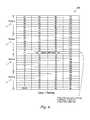
- FIG. 5shows a single section 500 of a memory such as memory 300 or the like.
- the section 500is in this embodiment a 64 Megabit section containing two 32 Megabit subsections 501 and 503 .
- Subsection 501contains four partitions 502 , 504 , 506 , and 508 , and a sense amplifier section 518 positioned between groupings of two partitions as shown.
- Subsection 503contains four partitions 508 , 510 , 512 , 514 , and 516 as shown, and a sense amplifier section 520 positioned between groupings of two partitions as shown.
- datalines 522 and 524 for read and datalines 526 and 528 for algorithm (or algo) modesare used, as is shown in greater detail in FIG. 5 .
- the datalines 522 , 524 , 526 , and 528originate from a program/sense amplifier row (not shown) and cross a plurality of partitions.
- Datalines 522 and 526cross subsection 501 and partitions 502 , 504 , 506 , and 508 ; and datalines 524 and 528 cross subsection 503 and partitions 510 , 512 , 514 , and 516 .
- Each datalineis locally switched onto a partition's block bitline through pass gates of a particular block if the block is selected, as will be described in further detail below.
- FIG. 5shows within groups of partitions in a “stack” how spanning is accomplished for the handling of a single sense amplifier row and program row ( 518 and 520 ) for multiple partitions. Rows within partitions and blocks are independently driven, so a typical row decode for a memory is used to decode rows. Columns, however, are linked differently because the datalines for read and algorithm modes span multiple partitions. Using a common sense amplifier with multiple partitions uses datalines that span all partitions in the particular memory subsection. Datalines are dedicated to either a read or an algorithm operation, allowing independent operation of read and algorithm operations. Concurrent operations can then be performed in a single subsection provided the operations are performed in different partitions.
- FIG. 6shows further detail of the connections of separate read datalines 522 and algorithm datalines 524 to blocks 0-7 within one partition, for example partition 506 .
- Each blockmay be selected for read or algorithm modes as is shown in FIG. 6 . If a block is selected for a read mode, it's pass gate 602 connected to a Zrd signal is turned on, that is the Zrd signal goes high. At the same time, since concurrent operations cannot happen in the same partition, the pass gate 604 connected to a Zalg signal is turned off, that is the Zalg signal goes low. In this situation, the dlcom line 606 is connected to the read dataline 522 .
- a blockIf a block is selected for an algorithm mode, it's pass gate 604 connected to the Zalg signal is turned on, that is the Zalg signal goes high. At the same time, since concurrent operations cannot happen in the same partition, the pass gate 602 connected to the Zrd signal is turned off, that is the Zrd signal goes low. In this situation, the dlcom line 606 is connected to the algorithm dataline 526 .
- the pass gate select signals Zalg and Zrdare block decoded to go high only if the particular block is selected.
- circuits inside each partitionkeep the Zrd signal from toggling if an algorithm is currently running in the selected block.
- Y and Z pass gates 608 for each blockdecode the YZ enable of every column of the block (column decoding).
- the independent devices 602 and 604are gate connected to the Zrd and Zalg signals for read and algorithm operations, respectively. Control circuitry on the gates of switches 602 and 604 have the lockouts.
- Drivers for the Y pass gates 610are drivers decoded by block select and partition select in typical fashion. That allows independent Z decoding, and reads on independent datalines without disturb issues.
- FIG. 7shows one embodiment 700 of a sense amplifier connection to allow simultaneous algorithm verifies and datasheet read operations.
- the read sense amplifiers 702 0 . . . 702 7are dedicated to read datalines, and one algorithm sense amplifier 704 per I/O is used for internal verifies during a program or erase operation. All circuits related to read and algorithm operations are separated and share only a common ground and supply connection. This prevents any events of one operation from affecting another operation.
- FIG. 7shows one I/O within a “stack” of multiple partitions. This is a local view of the block that is being accessed for a read operation.
- the grouping of 16 bitlines 706 0 . . . 706 7 , Y pass gates 708 0 . . . 708 7 , and Z pass gates 710 0 . . . 710 7is repeated for every block top to bottom.
- FIG. 7shows a grouping of every 16 bitlines 706 0 . . . 706 7 connected to a grouping of Y pass gates 708 0 . . . 708 7 , to Z pass gates 710 0 . . . 710 7 , and then to long datalines dl_read 0 . . . dl_read 7 that span multiple partitions into the grouping of read sense amplifiers 702 0 . . . 702 7 . Further from the grouping of Z pass gates 710 0 . . . 710 7 algorithm datalines dl_alg 0 . . . dl_alg 7 are connected to dedicated algorithm sense amplifier 704 .
- a single select algorithm signal in the group of signals sel_alg ⁇ 0 > . . . sel_alg ⁇ 7>, which are connected to the gates of the switches 712 0 . . . 712 7 respectively,is selected in this embodiment by an 8-1 multiplexor (not shown) that selects any one of the eight signals sel_alg ⁇ 0> . . . sel_alg ⁇ 7>.
- sel_alg ⁇ 7>maps the selected set of bitlines 706 0 . . . 706 7 to the algorithm sense amplifier 704 .
- the grouping of read datalines dl_read 0 . . . dl_read 7is connected to read sense amplifiers 702 0 . . . 702 7 . It should be understood that in this embodiment, eight read sense amplifiers are shown. The number of read sense amplifiers is dependent in large part upon the specification of the memory. If the specification of the memory is different, a different number of read sense amplifiers may be used, for example in page mode where a different page size is used.
- the various embodiments of the present inventionare amenable to use with memory devices having concurrent operations, including flash memories and the like, and to other devices with simultaneous read and program processes.
- a multi-partition architecture for concurrent operationhas been described that includes using a common program path and read paths to cover multiple partitions.
- the use of common program path and read paths for multiple partitionsreduces the amount of circuitry die size used, and allows for the maintenance of die size.
Landscapes
- Engineering & Computer Science (AREA)
- Microelectronics & Electronic Packaging (AREA)
- Read Only Memory (AREA)
Abstract
Description
- The present invention relates generally to memories and in particular the present invention relates to memory architecture.
- In flash memory products, it is common to design in functionality which supports concurrent operation between partitions or banks of flash memory. Each partition is typically a grouping of several blocks. Each block is individually accessible for program, eras, and read operations. Concurrent operation is dual operation in two different partitions simultaneously. For example, one block in one partition is being read which a different block in a different partition is being programmed or erased. Concurrency operations have been handled in the prior art by having an individual circuit for each partition, as is shown in the
partition architecture 100 ofFIG. 1 .Partition 100 includesdata sectors 102, and row drivers, column pass gates, predecoders, andtimers 104. Sense amps are dedicated by partitions, andcircuits 106 to program sense amplifiers for read operations and the like are all dedicated by partition. The circuits for each partition can program or read blocks in that partition. The circuits necessary for read and program operations are repeated for each partition block, such aspartition blocks device 200 shown inFIG. 2 . A flash device with 16 partitions has 16 groupings of circuits, one for each partition, with each circuit individually capable of program or read operations as shown inFIG. 1 . FIG. 2 shows amemory 200 with 32 partitions. Thismemory 202 therefore has 32 program rows as well as 32 sense amp rows. Memories such as this can quickly become very large as density increases.- With concurrent operational memories requiring an individual circuit for each partition block, and with the increasing density of memories and therefore the increasing number of partitions and memory blocks of current memories, individual circuitry for each partition block can cause serious issues with respect to die size. Further, as memory densities continue to increase, such an architecture may effectively limit memory density to below that which is available in order to maintain die size.
- For the reasons stated above, and for other reasons stated below which will become apparent to those skilled in the art upon reading and understanding the present specification, there is a need in the art for a memory architecture that reduces real estate overhead in the memory, and improving functionality while maintaining die size.
- The above-mentioned problems with concurrent operation in memories, increasing memory size and other problems are addressed by the present invention and will be understood by reading and studying the following specification.
- In one embodiment, a multiple partition memory architecture includes a number of partitions of memory cells, a number of groups of at least two partitions, a common program path and sense path circuit for each of the groups, and multiple separate read and algorithm datalines, each of the read and algorithm datalines spanning one of the groups and its common program path and sense path circuit.
- In another embodiment, a method of reducing circuit overhead in a multiple partition memory includes providing a memory divided into a number of partitions, arranging the partitions into groups of at least two partitions, providing a common program path and sense path circuit for each of the groups, providing separate read and algorithm datalines, each of the read and algorithm datalines spanning one of the groups and its common program path and sense path circuit, and allowing a concurrent operation on any partition not already in operation.
- In yet another embodiment, a processing system includes a processor and a memory coupled to the processor to store data provided by the processor and to provide data to the processor. The memory includes an array of memory cells addressable by address circuitry and input output circuitry, and control circuitry to read, write and erase the memory cells. The control circuitry includes a multiple partition memory architecture having a number of partitions of memory cells, a number of groups of at least two partitions, a common program path and sense path circuit for each of the groups, and separate read and algorithm datalines, each of the read and algorithm datalines spanning one of the groups and its common program path and sense path circuit.
- Other embodiments are described and claimed.
FIG. 1 is a block diagram of a typical prior art partition architecture;FIG. 2 is a block diagram of a typical prior art memory using the architecture ofFIG. 1 ;FIG. 3 is a block diagram of a partition placement according to one embodiment of the present invention;FIG. 4 is a block diagram of block placement in a memory according to another embodiment of the present invention;FIG. 5 is a block diagram of a portion of a memory according to another embodiment of the present invention;FIG. 6 is a diagram of pass gate connections to a partition according to another embodiment of the present invention; andFIG. 7 is a diagram of a column decode structure according to another embodiment of the present invention.- In the following detailed description of the invention, reference is made to the accompanying drawings that form a part hereof, and in which is shown, by way of illustration, specific embodiments in which the invention may be practiced. In the drawings, like numerals describe substantially similar components throughout the several views. These embodiments are described in sufficient detail to enable those skilled in the art to practice the invention. Other embodiments may be utilized and structural, logical, and electrical changes may be made without departing from the scope of the present invention.
- The following detailed description is, therefore, not to be taken in a limiting sense, and the scope of the present invention is defined only by the appended claims, along with the full scope of equivalents to which such claims are entitled.
- The embodiments of the present invention reduce the amount of circuit overhead necessary for concurrent operation. This is accomplished in various embodiments by employing common program path and sense (or read) path circuits, which allow concurrent operation of many different partitions.
- Referring to
FIG. 3 , a partition placement of architectures in amemory 300 is shown. In this example, eachsegment memory 300 has four partitions and a single program/sense amp row.Segment 302 comprises in this embodiment partitions labeled 0, 1, 2, and 3.Segment 304 comprises in this embodiment partitions labeled 4, 5, 6, and 7.Segment 306 comprises in this embodiment partitions labeled 8, 9, 10, and 11.Segment 308 comprises in this embodiment partitions labeled 12, 13, 14, and 15. Eachsegment segment program row - Each segment (or “stack”) of partitions has its own set of sense amplifiers and program pathways. In the embodiment shown, four partitions are “stacked,” but it should be understood that the number of partitions “stacked” is largely dependent upon the size of the die. Any number of stacked partitions could be used. The number of partitions which can be accessed by a single program pathway/sense amp row such as
rows - The space savings of these embodiments is large, since only one set of program/sense circuits are needed where four or more were previously required. Since there is a single program/sense amp row and circuitry for multiple partitions, the circuitry can be designed with a number of features or options that previously would have been too complex and would have occupied too much real estate on the die to be feasibly incorporated into a memory. This is due to the physical number of circuits being reduced. The reduction in the number of circuits results in a much smaller impact on overall die size.
- Block placement for blocks within partitions is shown in one embodiment in
FIG. 4 .Memory 300 is shown inFIG. 4 with the various partitions 0-15 broken down into eight main blocks for each partition. For example, blocks 24-31 comprisepartition 3. It should be understood that eight blocks per partition is shown by way of example and not by way of limitation. A different number of blocks, such as 4, 16, 32 or the like is within the scope of the present invention, and is determined in part by current and changing industry specifications. - To accomplish the various embodiments of the present invention, a structure such as that shown in
FIG. 5 is used.FIG. 5 shows asingle section 500 of a memory such asmemory 300 or the like. Thesection 500 is in this embodiment a 64 Megabit section containing two 32Megabit subsections Subsection 501 contains fourpartitions sense amplifier section 518 positioned between groupings of two partitions as shown.Subsection 503 contains fourpartitions sense amplifier section 520 positioned between groupings of two partitions as shown. In order to allow concurrent operations across multiple partitions,separate datalines FIG. 5 . Thedatalines Datalines cross subsection 501 andpartitions cross subsection 503 andpartitions FIG. 5 shows within groups of partitions in a “stack” how spanning is accomplished for the handling of a single sense amplifier row and program row (518 and520) for multiple partitions. Rows within partitions and blocks are independently driven, so a typical row decode for a memory is used to decode rows. Columns, however, are linked differently because the datalines for read and algorithm modes span multiple partitions. Using a common sense amplifier with multiple partitions uses datalines that span all partitions in the particular memory subsection. Datalines are dedicated to either a read or an algorithm operation, allowing independent operation of read and algorithm operations. Concurrent operations can then be performed in a single subsection provided the operations are performed in different partitions.FIG. 6 shows further detail of the connections of separate read datalines522 andalgorithm datalines 524 to blocks 0-7 within one partition, forexample partition 506. Each block may be selected for read or algorithm modes as is shown inFIG. 6 . If a block is selected for a read mode, it'spass gate 602 connected to a Zrd signal is turned on, that is the Zrd signal goes high. At the same time, since concurrent operations cannot happen in the same partition, thepass gate 604 connected to a Zalg signal is turned off, that is the Zalg signal goes low. In this situation, thedlcom line 606 is connected to theread dataline 522. If a block is selected for an algorithm mode, it'spass gate 604 connected to the Zalg signal is turned on, that is the Zalg signal goes high. At the same time, since concurrent operations cannot happen in the same partition, thepass gate 602 connected to the Zrd signal is turned off, that is the Zrd signal goes low. In this situation, thedlcom line 606 is connected to thealgorithm dataline 526.- The pass gate select signals Zalg and Zrd are block decoded to go high only if the particular block is selected. In one embodiment, circuits inside each partition keep the Zrd signal from toggling if an algorithm is currently running in the selected block. There is a lockout based on the algorithm mode in one embodiment, so if an algorithm is running, the block is prevented from any random access. Y and
Z pass gates 608 for each block decode the YZ enable of every column of the block (column decoding). Theindependent devices switches Y pass gates 610 are drivers decoded by block select and partition select in typical fashion. That allows independent Z decoding, and reads on independent datalines without disturb issues. FIG. 7 shows oneembodiment 700 of a sense amplifier connection to allow simultaneous algorithm verifies and datasheet read operations. In one embodiment, the read sense amplifiers7020. . .7027are dedicated to read datalines, and onealgorithm sense amplifier 704 per I/O is used for internal verifies during a program or erase operation. All circuits related to read and algorithm operations are separated and share only a common ground and supply connection. This prevents any events of one operation from affecting another operation.FIG. 7 shows one I/O within a “stack” of multiple partitions. This is a local view of the block that is being accessed for a read operation. The grouping of 16 bitlines7060. . .7067, Y pass gates7080. . .7087, and Z pass gates7100. . .7107is repeated for every block top to bottom.FIG. 7 shows a grouping of every 16 bitlines7060. . .7067connected to a grouping of Y pass gates7080. . .7087, to Z pass gates7100. . .7107, and then to long datalines dl_read0 . . . dl_read7 that span multiple partitions into the grouping of read sense amplifiers7020. . .7027. Further from the grouping of Z pass gates7100. . .7107algorithm datalines dl_alg0 . . . dl_alg7 are connected to dedicatedalgorithm sense amplifier 704. There is onealgorithm sense amplifier 704 per I/O. A group of switches7120. . .7127are connected between the Z pass gates7100. . .7107andalgorithm sense amplifier 704. A single select algorithm signal in the group of signals sel_alg<0 > . . . sel_alg<7>, which are connected to the gates of the switches7120. . .7127respectively, is selected in this embodiment by an 8-1 multiplexor (not shown) that selects any one of the eight signals sel_alg<0> . . . sel_alg<7>. The selection of one of the eight signals sel_alg<0> . . . sel_alg<7> maps the selected set of bitlines7060. . .7067to thealgorithm sense amplifier 704. The grouping of read datalines dl_read0 . . . dl_read7 is connected to read sense amplifiers7020. . .7027. It should be understood that in this embodiment, eight read sense amplifiers are shown. The number of read sense amplifiers is dependent in large part upon the specification of the memory. If the specification of the memory is different, a different number of read sense amplifiers may be used, for example in page mode where a different page size is used.- The various embodiments of the present invention are amenable to use with memory devices having concurrent operations, including flash memories and the like, and to other devices with simultaneous read and program processes.
- A multi-partition architecture for concurrent operation has been described that includes using a common program path and read paths to cover multiple partitions. The use of common program path and read paths for multiple partitions reduces the amount of circuitry die size used, and allows for the maintenance of die size.
- Although specific embodiments have been illustrated and described herein, it will be appreciated by those of ordinary skill in the art that any arrangement, which is calculated to achieve the same purpose, may be substituted for the specific embodiment shown. This application is intended to cover any adaptations or variations of the present invention. Therefore, it is manifestly intended that this invention be limited only by the claims and the equivalents thereof.
Claims (25)
Priority Applications (2)
| Application Number | Priority Date | Filing Date | Title |
|---|---|---|---|
| US10/683,075US8233322B2 (en) | 2003-10-10 | 2003-10-10 | Multi-partition memory with separated read and algorithm datalines |
| US13/561,519US20120294085A1 (en) | 2003-10-10 | 2012-07-30 | Multi-partition architecture for memory |
Applications Claiming Priority (1)
| Application Number | Priority Date | Filing Date | Title |
|---|---|---|---|
| US10/683,075US8233322B2 (en) | 2003-10-10 | 2003-10-10 | Multi-partition memory with separated read and algorithm datalines |
Related Child Applications (1)
| Application Number | Title | Priority Date | Filing Date |
|---|---|---|---|
| US13/561,519ContinuationUS20120294085A1 (en) | 2003-10-10 | 2012-07-30 | Multi-partition architecture for memory |
Publications (2)
| Publication Number | Publication Date |
|---|---|
| US20050081013A1true US20050081013A1 (en) | 2005-04-14 |
| US8233322B2 US8233322B2 (en) | 2012-07-31 |
Family
ID=34422654
Family Applications (2)
| Application Number | Title | Priority Date | Filing Date |
|---|---|---|---|
| US10/683,075Expired - LifetimeUS8233322B2 (en) | 2003-10-10 | 2003-10-10 | Multi-partition memory with separated read and algorithm datalines |
| US13/561,519AbandonedUS20120294085A1 (en) | 2003-10-10 | 2012-07-30 | Multi-partition architecture for memory |
Family Applications After (1)
| Application Number | Title | Priority Date | Filing Date |
|---|---|---|---|
| US13/561,519AbandonedUS20120294085A1 (en) | 2003-10-10 | 2012-07-30 | Multi-partition architecture for memory |
Country Status (1)
| Country | Link |
|---|---|
| US (2) | US8233322B2 (en) |
Cited By (5)
| Publication number | Priority date | Publication date | Assignee | Title |
|---|---|---|---|---|
| US20090067276A1 (en)* | 2007-09-11 | 2009-03-12 | Micron Technology, Inc. | Storing Operational Information in an Array of Memory Cells |
| WO2012168954A1 (en) | 2011-06-10 | 2012-12-13 | Micron Technology Inc. | Apparatus and methods to perform read-while write (rww) operations |
| WO2017123413A1 (en)* | 2016-01-11 | 2017-07-20 | Micron Technology, Inc. | Apparatuses and methods for concurrently accessing multiple partitions of a non-volatile memory |
| US20180166130A1 (en)* | 2015-05-14 | 2018-06-14 | Adesto Technologies Corporation | Concurrent read and reconfigured write operations in a memory device |
| US20220365695A1 (en)* | 2021-05-14 | 2022-11-17 | Nanjing Semidrive Technology Ltd. | Data processing method and device and electronic apparatus |
Citations (13)
| Publication number | Priority date | Publication date | Assignee | Title |
|---|---|---|---|---|
| US5570319A (en)* | 1992-10-14 | 1996-10-29 | Sun Microsystems, Inc. | Embedded access trees for memory arrays |
| US5675529A (en)* | 1995-07-07 | 1997-10-07 | Sun Microsystems, Inc. | Fast access memory array |
| US5847994A (en)* | 1997-09-08 | 1998-12-08 | Mitsubishi Denki Kabushiki Kaisha | Non-volatile semiconductor memory device having a back ground operation mode |
| US5894437A (en)* | 1998-01-23 | 1999-04-13 | Hyundai Elecronics America, Inc. | Concurrent read/write architecture for a flash memory |
| US6058461A (en)* | 1997-12-02 | 2000-05-02 | Advanced Micro Devices, Inc. | Computer system including priorities for memory operations and allowing a higher priority memory operation to interrupt a lower priority memory operation |
| US6292392B1 (en)* | 1997-09-30 | 2001-09-18 | Sharp Kabushiki Kaisha | Non-volatile semiconductor device |
| US6480929B1 (en)* | 1998-10-31 | 2002-11-12 | Advanced Micro Devices Inc. | Pseudo-concurrency between a volatile memory and a non-volatile memory on a same data bus |
| US6529409B1 (en)* | 2001-09-10 | 2003-03-04 | Silicon Storage Technology, Inc. | Integrated circuit for concurrent flash memory with uneven array architecture |
| US6587917B2 (en)* | 2001-05-29 | 2003-07-01 | Agilent Technologies, Inc. | Memory architecture for supporting concurrent access of different types |
| US6614685B2 (en)* | 2001-08-09 | 2003-09-02 | Multi Level Memory Technology | Flash memory array partitioning architectures |
| US6643212B1 (en)* | 2002-04-18 | 2003-11-04 | United Memories, Inc. | Simultaneous function dynamic random access memory device technique |
| US6822900B2 (en)* | 2001-04-13 | 2004-11-23 | Seiko Epson Corporation | Non-volatile semiconductor memory device |
| US6829194B2 (en)* | 1999-05-10 | 2004-12-07 | Kabushiki Kaisha Toshiba | Semiconductor device that enables simultaneous read and write/read operation |
- 2003
- 2003-10-10USUS10/683,075patent/US8233322B2/ennot_activeExpired - Lifetime
- 2012
- 2012-07-30USUS13/561,519patent/US20120294085A1/ennot_activeAbandoned
Patent Citations (13)
| Publication number | Priority date | Publication date | Assignee | Title |
|---|---|---|---|---|
| US5570319A (en)* | 1992-10-14 | 1996-10-29 | Sun Microsystems, Inc. | Embedded access trees for memory arrays |
| US5675529A (en)* | 1995-07-07 | 1997-10-07 | Sun Microsystems, Inc. | Fast access memory array |
| US5847994A (en)* | 1997-09-08 | 1998-12-08 | Mitsubishi Denki Kabushiki Kaisha | Non-volatile semiconductor memory device having a back ground operation mode |
| US6292392B1 (en)* | 1997-09-30 | 2001-09-18 | Sharp Kabushiki Kaisha | Non-volatile semiconductor device |
| US6058461A (en)* | 1997-12-02 | 2000-05-02 | Advanced Micro Devices, Inc. | Computer system including priorities for memory operations and allowing a higher priority memory operation to interrupt a lower priority memory operation |
| US5894437A (en)* | 1998-01-23 | 1999-04-13 | Hyundai Elecronics America, Inc. | Concurrent read/write architecture for a flash memory |
| US6480929B1 (en)* | 1998-10-31 | 2002-11-12 | Advanced Micro Devices Inc. | Pseudo-concurrency between a volatile memory and a non-volatile memory on a same data bus |
| US6829194B2 (en)* | 1999-05-10 | 2004-12-07 | Kabushiki Kaisha Toshiba | Semiconductor device that enables simultaneous read and write/read operation |
| US6822900B2 (en)* | 2001-04-13 | 2004-11-23 | Seiko Epson Corporation | Non-volatile semiconductor memory device |
| US6587917B2 (en)* | 2001-05-29 | 2003-07-01 | Agilent Technologies, Inc. | Memory architecture for supporting concurrent access of different types |
| US6614685B2 (en)* | 2001-08-09 | 2003-09-02 | Multi Level Memory Technology | Flash memory array partitioning architectures |
| US6529409B1 (en)* | 2001-09-10 | 2003-03-04 | Silicon Storage Technology, Inc. | Integrated circuit for concurrent flash memory with uneven array architecture |
| US6643212B1 (en)* | 2002-04-18 | 2003-11-04 | United Memories, Inc. | Simultaneous function dynamic random access memory device technique |
Cited By (16)
| Publication number | Priority date | Publication date | Assignee | Title |
|---|---|---|---|---|
| US7876638B2 (en) | 2007-09-11 | 2011-01-25 | Micron Technology, Inc. | Storing operational information in an array of memory cells |
| US20110199824A1 (en)* | 2007-09-11 | 2011-08-18 | Micron Technology, Inc. | Storing operational information in an array of memory cells |
| US8437217B2 (en) | 2007-09-11 | 2013-05-07 | Micron Technology, Inc. | Storing operational information in an array of memory cells |
| US20090067276A1 (en)* | 2007-09-11 | 2009-03-12 | Micron Technology, Inc. | Storing Operational Information in an Array of Memory Cells |
| US9767857B2 (en) | 2011-06-10 | 2017-09-19 | Micron Technology, Inc. | Apparatus and methods to perform read-while write (RWW) operations |
| WO2012168954A1 (en) | 2011-06-10 | 2012-12-13 | Micron Technology Inc. | Apparatus and methods to perform read-while write (rww) operations |
| US8995161B2 (en) | 2011-06-10 | 2015-03-31 | Micron Technology, Inc. | Apparatus and methods to perform read-while write (RWW) operations |
| US20180166130A1 (en)* | 2015-05-14 | 2018-06-14 | Adesto Technologies Corporation | Concurrent read and reconfigured write operations in a memory device |
| US10636480B2 (en)* | 2015-05-14 | 2020-04-28 | Adesto Technologies Corporation | Concurrent read and reconfigured write operations in a memory device |
| US11094375B2 (en) | 2015-05-14 | 2021-08-17 | Adesto Technologies Corporation | Concurrent read and reconfigured write operations in a memory device |
| WO2017123413A1 (en)* | 2016-01-11 | 2017-07-20 | Micron Technology, Inc. | Apparatuses and methods for concurrently accessing multiple partitions of a non-volatile memory |
| US10719237B2 (en) | 2016-01-11 | 2020-07-21 | Micron Technology, Inc. | Apparatuses and methods for concurrently accessing multiple partitions of a non-volatile memory |
| US11354040B2 (en) | 2016-01-11 | 2022-06-07 | Micron Technology, Inc. | Apparatuses and methods for concurrently accessing multiple partitions of a non-volatile memory |
| US11768603B2 (en) | 2016-01-11 | 2023-09-26 | Micron Technology, Inc. | Apparatuses and methods for concurrently accessing multiple partitions of a non-volatile memory |
| US20220365695A1 (en)* | 2021-05-14 | 2022-11-17 | Nanjing Semidrive Technology Ltd. | Data processing method and device and electronic apparatus |
| US12045488B2 (en)* | 2021-05-14 | 2024-07-23 | Nanjing Semidrive Technology Ltd. | Data processing method and device and electronic apparatus |
Also Published As
| Publication number | Publication date |
|---|---|
| US8233322B2 (en) | 2012-07-31 |
| US20120294085A1 (en) | 2012-11-22 |
Similar Documents
| Publication | Publication Date | Title |
|---|---|---|
| US7079417B2 (en) | Read-while-write flash memory devices having local row decoder circuits activated by separate read and write signals | |
| EP1397808B1 (en) | Steering gate and bit line segmentation in non-volatile memories | |
| US7580284B2 (en) | Flash memory devices and methods of programming the same by overlapping programming operations for multiple mats | |
| KR0179361B1 (en) | Bitline segmentation in logic memory arrays c 16/06 | |
| US20120294085A1 (en) | Multi-partition architecture for memory | |
| US6480417B2 (en) | Global/local memory decode with independent program and read paths and shared local decode | |
| US20080031075A1 (en) | Memory architecture with advanced main-bitline partitioning circuitry for enhanced erase/program/verify operations | |
| US8467252B2 (en) | Word line activation in memory devices | |
| US6026021A (en) | Semiconductor memory array partitioned into memory blocks and sub-blocks and method of addressing | |
| US8971129B2 (en) | NROM device with reduced power unit | |
| US20100070676A1 (en) | Memory Data Bus Placement and Control | |
| US6950337B2 (en) | Nonvolatile memory device with simultaneous read/write | |
| US6529409B1 (en) | Integrated circuit for concurrent flash memory with uneven array architecture | |
| US6631089B1 (en) | Bit line decoding scheme and circuit for dual bit memory array | |
| US5982680A (en) | Semiconductor memory | |
| US7646644B2 (en) | Nonvolatile memory device with multiple references and corresponding control method | |
| JPH06195964A (en) | Semiconductor memory | |
| KR20020017307A (en) | Semiconductor memory device of multi bank structure | |
| KR20050020188A (en) | Memory system sharing a plurality of memory chips and its programming method | |
| KR20070061479A (en) | Redundancy Control Method of Semiconductor Memory Device and Semiconductor Memory Device | |
| JP2004348857A (en) | Semiconductor device |
Legal Events
| Date | Code | Title | Description |
|---|---|---|---|
| AS | Assignment | Owner name:MICRON TECHNOLOGY, INC., IDAHO Free format text:ASSIGNMENT OF ASSIGNORS INTEREST;ASSIGNORS:PEKNY, THEODORE T.;GUALANDRI, STEPHEN J.;REEL/FRAME:014602/0353 Effective date:20031001 | |
| FEPP | Fee payment procedure | Free format text:PAYOR NUMBER ASSIGNED (ORIGINAL EVENT CODE: ASPN); ENTITY STATUS OF PATENT OWNER: LARGE ENTITY | |
| STCF | Information on status: patent grant | Free format text:PATENTED CASE | |
| CC | Certificate of correction | ||
| FPAY | Fee payment | Year of fee payment:4 | |
| AS | Assignment | Owner name:U.S. BANK NATIONAL ASSOCIATION, AS COLLATERAL AGENT, CALIFORNIA Free format text:SECURITY INTEREST;ASSIGNOR:MICRON TECHNOLOGY, INC.;REEL/FRAME:038669/0001 Effective date:20160426 Owner name:U.S. BANK NATIONAL ASSOCIATION, AS COLLATERAL AGEN Free format text:SECURITY INTEREST;ASSIGNOR:MICRON TECHNOLOGY, INC.;REEL/FRAME:038669/0001 Effective date:20160426 | |
| AS | Assignment | Owner name:MORGAN STANLEY SENIOR FUNDING, INC., AS COLLATERAL AGENT, MARYLAND Free format text:PATENT SECURITY AGREEMENT;ASSIGNOR:MICRON TECHNOLOGY, INC.;REEL/FRAME:038954/0001 Effective date:20160426 Owner name:MORGAN STANLEY SENIOR FUNDING, INC., AS COLLATERAL Free format text:PATENT SECURITY AGREEMENT;ASSIGNOR:MICRON TECHNOLOGY, INC.;REEL/FRAME:038954/0001 Effective date:20160426 | |
| AS | Assignment | Owner name:U.S. BANK NATIONAL ASSOCIATION, AS COLLATERAL AGENT, CALIFORNIA Free format text:CORRECTIVE ASSIGNMENT TO CORRECT THE REPLACE ERRONEOUSLY FILED PATENT #7358718 WITH THE CORRECT PATENT #7358178 PREVIOUSLY RECORDED ON REEL 038669 FRAME 0001. ASSIGNOR(S) HEREBY CONFIRMS THE SECURITY INTEREST;ASSIGNOR:MICRON TECHNOLOGY, INC.;REEL/FRAME:043079/0001 Effective date:20160426 Owner name:U.S. BANK NATIONAL ASSOCIATION, AS COLLATERAL AGEN Free format text:CORRECTIVE ASSIGNMENT TO CORRECT THE REPLACE ERRONEOUSLY FILED PATENT #7358718 WITH THE CORRECT PATENT #7358178 PREVIOUSLY RECORDED ON REEL 038669 FRAME 0001. ASSIGNOR(S) HEREBY CONFIRMS THE SECURITY INTEREST;ASSIGNOR:MICRON TECHNOLOGY, INC.;REEL/FRAME:043079/0001 Effective date:20160426 | |
| AS | Assignment | Owner name:JPMORGAN CHASE BANK, N.A., AS COLLATERAL AGENT, ILLINOIS Free format text:SECURITY INTEREST;ASSIGNORS:MICRON TECHNOLOGY, INC.;MICRON SEMICONDUCTOR PRODUCTS, INC.;REEL/FRAME:047540/0001 Effective date:20180703 Owner name:JPMORGAN CHASE BANK, N.A., AS COLLATERAL AGENT, IL Free format text:SECURITY INTEREST;ASSIGNORS:MICRON TECHNOLOGY, INC.;MICRON SEMICONDUCTOR PRODUCTS, INC.;REEL/FRAME:047540/0001 Effective date:20180703 | |
| AS | Assignment | Owner name:MICRON TECHNOLOGY, INC., IDAHO Free format text:RELEASE BY SECURED PARTY;ASSIGNOR:U.S. BANK NATIONAL ASSOCIATION, AS COLLATERAL AGENT;REEL/FRAME:047243/0001 Effective date:20180629 | |
| AS | Assignment | Owner name:MICRON TECHNOLOGY, INC., IDAHO Free format text:RELEASE BY SECURED PARTY;ASSIGNOR:MORGAN STANLEY SENIOR FUNDING, INC., AS COLLATERAL AGENT;REEL/FRAME:050937/0001 Effective date:20190731 | |
| AS | Assignment | Owner name:MICRON SEMICONDUCTOR PRODUCTS, INC., IDAHO Free format text:RELEASE BY SECURED PARTY;ASSIGNOR:JPMORGAN CHASE BANK, N.A., AS COLLATERAL AGENT;REEL/FRAME:051028/0001 Effective date:20190731 Owner name:MICRON TECHNOLOGY, INC., IDAHO Free format text:RELEASE BY SECURED PARTY;ASSIGNOR:JPMORGAN CHASE BANK, N.A., AS COLLATERAL AGENT;REEL/FRAME:051028/0001 Effective date:20190731 | |
| MAFP | Maintenance fee payment | Free format text:PAYMENT OF MAINTENANCE FEE, 8TH YEAR, LARGE ENTITY (ORIGINAL EVENT CODE: M1552); ENTITY STATUS OF PATENT OWNER: LARGE ENTITY Year of fee payment:8 | |
| MAFP | Maintenance fee payment | Free format text:PAYMENT OF MAINTENANCE FEE, 12TH YEAR, LARGE ENTITY (ORIGINAL EVENT CODE: M1553); ENTITY STATUS OF PATENT OWNER: LARGE ENTITY Year of fee payment:12 |