US20050079706A1 - Dual damascene structure and method - Google Patents
Dual damascene structure and methodDownload PDFInfo
- Publication number
- US20050079706A1 US20050079706A1US10/685,055US68505503AUS2005079706A1US 20050079706 A1US20050079706 A1US 20050079706A1US 68505503 AUS68505503 AUS 68505503AUS 2005079706 A1US2005079706 A1US 2005079706A1
- Authority
- US
- United States
- Prior art keywords
- dielectric material
- pattern
- mask layer
- layer
- depositing
- Prior art date
- Legal status (The legal status is an assumption and is not a legal conclusion. Google has not performed a legal analysis and makes no representation as to the accuracy of the status listed.)
- Granted
Links
- 238000000034methodMethods0.000titleclaimsabstractdescription150
- 230000009977dual effectEffects0.000titleabstractdescription45
- 239000003989dielectric materialSubstances0.000claimsabstractdescription192
- 239000004065semiconductorSubstances0.000claimsabstractdescription40
- 238000004140cleaningMethods0.000claimsabstractdescription35
- 238000004519manufacturing processMethods0.000claimsabstractdescription16
- 229910010272inorganic materialInorganic materials0.000claimsabstractdescription8
- 239000011147inorganic materialSubstances0.000claimsabstractdescription8
- 239000011368organic materialSubstances0.000claimsabstractdescription5
- 239000000463materialSubstances0.000claimsdescription49
- 229920002120photoresistant polymerPolymers0.000claimsdescription46
- 238000000151depositionMethods0.000claimsdescription40
- 238000000059patterningMethods0.000claimsdescription33
- 229910004012SiCxInorganic materials0.000claimsdescription28
- RYGMFSIKBFXOCR-UHFFFAOYSA-NCopperChemical compound[Cu]RYGMFSIKBFXOCR-UHFFFAOYSA-N0.000claimsdescription17
- 229910052802copperInorganic materials0.000claimsdescription17
- 239000010949copperSubstances0.000claimsdescription17
- 239000004020conductorSubstances0.000claimsdescription16
- VYPSYNLAJGMNEJ-UHFFFAOYSA-NSilicium dioxideChemical compoundO=[Si]=OVYPSYNLAJGMNEJ-UHFFFAOYSA-N0.000claimsdescription13
- 229920000642polymerPolymers0.000claimsdescription11
- 239000006117anti-reflective coatingSubstances0.000claimsdescription10
- 238000005530etchingMethods0.000claimsdescription10
- 239000000377silicon dioxideSubstances0.000claimsdescription6
- 229910052681coesiteInorganic materials0.000claimsdescription5
- 229910052906cristobaliteInorganic materials0.000claimsdescription5
- 229910052682stishoviteInorganic materials0.000claimsdescription5
- 229910052905tridymiteInorganic materials0.000claimsdescription5
- 238000005389semiconductor device fabricationMethods0.000claimsdescription4
- 229910020776SixNyInorganic materials0.000claimsdescription3
- 239000011521glassSubstances0.000claimsdescription3
- 150000004767nitridesChemical class0.000claimsdescription3
- 239000003870refractory metalSubstances0.000claimsdescription3
- 239000005368silicate glassSubstances0.000claimsdescription3
- 230000008569processEffects0.000description65
- 239000007789gasSubstances0.000description30
- 210000002381plasmaAnatomy0.000description19
- 235000012431wafersNutrition0.000description16
- 230000008901benefitEffects0.000description13
- 238000005229chemical vapour depositionMethods0.000description10
- 231100000572poisoningToxicity0.000description10
- 230000000607poisoning effectEffects0.000description10
- 229910052782aluminiumInorganic materials0.000description5
- XAGFODPZIPBFFR-UHFFFAOYSA-NaluminiumChemical compound[Al]XAGFODPZIPBFFR-UHFFFAOYSA-N0.000description5
- 239000011810insulating materialSubstances0.000description5
- 230000004888barrier functionEffects0.000description4
- 238000003682fluorination reactionMethods0.000description4
- 238000011065in-situ storageMethods0.000description4
- 239000011261inert gasSubstances0.000description4
- 238000001459lithographyMethods0.000description4
- 238000001465metallisationMethods0.000description4
- 239000000758substrateSubstances0.000description4
- 229910052581Si3N4Inorganic materials0.000description3
- QVGXLLKOCUKJST-UHFFFAOYSA-Natomic oxygenChemical compound[O]QVGXLLKOCUKJST-UHFFFAOYSA-N0.000description3
- 238000009792diffusion processMethods0.000description3
- RWRIWBAIICGTTQ-UHFFFAOYSA-NdifluoromethaneChemical compoundFCFRWRIWBAIICGTTQ-UHFFFAOYSA-N0.000description3
- 230000003116impacting effectEffects0.000description3
- 230000010354integrationEffects0.000description3
- 239000000203mixtureSubstances0.000description3
- 239000001301oxygenSubstances0.000description3
- 229910052760oxygenInorganic materials0.000description3
- 229910052710siliconInorganic materials0.000description3
- 239000010703siliconSubstances0.000description3
- HBMJWWWQQXIZIP-UHFFFAOYSA-Nsilicon carbideChemical compound[Si+]#[C-]HBMJWWWQQXIZIP-UHFFFAOYSA-N0.000description3
- 229910010271silicon carbideInorganic materials0.000description3
- 241000894007speciesSpecies0.000description3
- 239000000126substanceSubstances0.000description3
- IJGRMHOSHXDMSA-UHFFFAOYSA-NAtomic nitrogenChemical compoundN#NIJGRMHOSHXDMSA-UHFFFAOYSA-N0.000description2
- 229910004294SiNxHyInorganic materials0.000description2
- 239000002318adhesion promoterSubstances0.000description2
- 150000001412aminesChemical class0.000description2
- 230000015572biosynthetic processEffects0.000description2
- 230000008859changeEffects0.000description2
- 230000008021depositionEffects0.000description2
- 230000000694effectsEffects0.000description2
- NBVXSUQYWXRMNV-UHFFFAOYSA-NfluoromethaneChemical compoundFCNBVXSUQYWXRMNV-UHFFFAOYSA-N0.000description2
- 238000012986modificationMethods0.000description2
- 230000004048modificationEffects0.000description2
- 239000011148porous materialSubstances0.000description2
- 238000002203pretreatmentMethods0.000description2
- 230000001737promoting effectEffects0.000description2
- 229910000838Al alloyInorganic materials0.000description1
- 244000025254Cannabis sativaSpecies0.000description1
- OKTJSMMVPCPJKN-UHFFFAOYSA-NCarbonChemical compound[C]OKTJSMMVPCPJKN-UHFFFAOYSA-N0.000description1
- 229910000881Cu alloyInorganic materials0.000description1
- XPDWGBQVDMORPB-UHFFFAOYSA-NFluoroformChemical compoundFC(F)FXPDWGBQVDMORPB-UHFFFAOYSA-N0.000description1
- 229910001218Gallium arsenideInorganic materials0.000description1
- UFHFLCQGNIYNRP-UHFFFAOYSA-NHydrogenChemical compound[H][H]UFHFLCQGNIYNRP-UHFFFAOYSA-N0.000description1
- XUIMIQQOPSSXEZ-UHFFFAOYSA-NSiliconChemical compound[Si]XUIMIQQOPSSXEZ-UHFFFAOYSA-N0.000description1
- 229910004156TaNxInorganic materials0.000description1
- -1TaNx as an exampleChemical class0.000description1
- 230000004075alterationEffects0.000description1
- 229910052799carbonInorganic materials0.000description1
- 229910002091carbon monoxideInorganic materials0.000description1
- 150000001875compoundsChemical class0.000description1
- 238000010276constructionMethods0.000description1
- 230000007797corrosionEffects0.000description1
- 238000005260corrosionMethods0.000description1
- 230000003247decreasing effectEffects0.000description1
- 230000032798delaminationEffects0.000description1
- 238000007772electroless platingMethods0.000description1
- 238000009713electroplatingMethods0.000description1
- 229920002313fluoropolymerPolymers0.000description1
- 239000004811fluoropolymerSubstances0.000description1
- 239000001257hydrogenSubstances0.000description1
- 229910052739hydrogenInorganic materials0.000description1
- 239000012212insulatorSubstances0.000description1
- 150000002500ionsChemical class0.000description1
- 229910052751metalInorganic materials0.000description1
- 239000002184metalSubstances0.000description1
- 229910021421monocrystalline siliconInorganic materials0.000description1
- 229910052757nitrogenInorganic materials0.000description1
- QJGQUHMNIGDVPM-UHFFFAOYSA-Nnitrogen groupChemical group[N]QJGQUHMNIGDVPM-UHFFFAOYSA-N0.000description1
- 238000000206photolithographyMethods0.000description1
- 230000000379polymerizing effectEffects0.000description1
- 239000000376reactantSubstances0.000description1
- 238000010008shearingMethods0.000description1
- 235000012239silicon dioxideNutrition0.000description1
- HQVNEWCFYHHQES-UHFFFAOYSA-Nsilicon nitrideChemical compoundN12[Si]34N5[Si]62N3[Si]51N64HQVNEWCFYHHQES-UHFFFAOYSA-N0.000description1
- 229910052814silicon oxideInorganic materials0.000description1
- 239000002002slurrySubstances0.000description1
- 238000006467substitution reactionMethods0.000description1
- 238000004148unit processMethods0.000description1
- XLYOFNOQVPJJNP-UHFFFAOYSA-NwaterSubstancesOXLYOFNOQVPJJNP-UHFFFAOYSA-N0.000description1
Images


Classifications
- H—ELECTRICITY
- H01—ELECTRIC ELEMENTS
- H01L—SEMICONDUCTOR DEVICES NOT COVERED BY CLASS H10
- H01L21/00—Processes or apparatus adapted for the manufacture or treatment of semiconductor or solid state devices or of parts thereof
- H01L21/70—Manufacture or treatment of devices consisting of a plurality of solid state components formed in or on a common substrate or of parts thereof; Manufacture of integrated circuit devices or of parts thereof
- H01L21/71—Manufacture of specific parts of devices defined in group H01L21/70
- H01L21/768—Applying interconnections to be used for carrying current between separate components within a device comprising conductors and dielectrics
- H01L21/76801—Applying interconnections to be used for carrying current between separate components within a device comprising conductors and dielectrics characterised by the formation and the after-treatment of the dielectrics, e.g. smoothing
- H01L21/76835—Combinations of two or more different dielectric layers having a low dielectric constant
- H—ELECTRICITY
- H01—ELECTRIC ELEMENTS
- H01J—ELECTRIC DISCHARGE TUBES OR DISCHARGE LAMPS
- H01J37/00—Discharge tubes with provision for introducing objects or material to be exposed to the discharge, e.g. for the purpose of examination or processing thereof
- H01J37/32—Gas-filled discharge tubes
- H01J37/32431—Constructional details of the reactor
- H01J37/32798—Further details of plasma apparatus not provided for in groups H01J37/3244 - H01J37/32788; special provisions for cleaning or maintenance of the apparatus
- H01J37/32853—Hygiene
- H01J37/32862—In situ cleaning of vessels and/or internal parts
- H—ELECTRICITY
- H01—ELECTRIC ELEMENTS
- H01L—SEMICONDUCTOR DEVICES NOT COVERED BY CLASS H10
- H01L21/00—Processes or apparatus adapted for the manufacture or treatment of semiconductor or solid state devices or of parts thereof
- H01L21/02—Manufacture or treatment of semiconductor devices or of parts thereof
- H01L21/04—Manufacture or treatment of semiconductor devices or of parts thereof the devices having potential barriers, e.g. a PN junction, depletion layer or carrier concentration layer
- H01L21/18—Manufacture or treatment of semiconductor devices or of parts thereof the devices having potential barriers, e.g. a PN junction, depletion layer or carrier concentration layer the devices having semiconductor bodies comprising elements of Group IV of the Periodic Table or AIIIBV compounds with or without impurities, e.g. doping materials
- H01L21/30—Treatment of semiconductor bodies using processes or apparatus not provided for in groups H01L21/20 - H01L21/26
- H01L21/31—Treatment of semiconductor bodies using processes or apparatus not provided for in groups H01L21/20 - H01L21/26 to form insulating layers thereon, e.g. for masking or by using photolithographic techniques; After treatment of these layers; Selection of materials for these layers
- H01L21/3105—After-treatment
- H01L21/311—Etching the insulating layers by chemical or physical means
- H01L21/31105—Etching inorganic layers
- H01L21/31111—Etching inorganic layers by chemical means
- H01L21/31116—Etching inorganic layers by chemical means by dry-etching
- H—ELECTRICITY
- H01—ELECTRIC ELEMENTS
- H01L—SEMICONDUCTOR DEVICES NOT COVERED BY CLASS H10
- H01L21/00—Processes or apparatus adapted for the manufacture or treatment of semiconductor or solid state devices or of parts thereof
- H01L21/02—Manufacture or treatment of semiconductor devices or of parts thereof
- H01L21/04—Manufacture or treatment of semiconductor devices or of parts thereof the devices having potential barriers, e.g. a PN junction, depletion layer or carrier concentration layer
- H01L21/18—Manufacture or treatment of semiconductor devices or of parts thereof the devices having potential barriers, e.g. a PN junction, depletion layer or carrier concentration layer the devices having semiconductor bodies comprising elements of Group IV of the Periodic Table or AIIIBV compounds with or without impurities, e.g. doping materials
- H01L21/30—Treatment of semiconductor bodies using processes or apparatus not provided for in groups H01L21/20 - H01L21/26
- H01L21/31—Treatment of semiconductor bodies using processes or apparatus not provided for in groups H01L21/20 - H01L21/26 to form insulating layers thereon, e.g. for masking or by using photolithographic techniques; After treatment of these layers; Selection of materials for these layers
- H01L21/3105—After-treatment
- H01L21/311—Etching the insulating layers by chemical or physical means
- H01L21/31127—Etching organic layers
- H01L21/31133—Etching organic layers by chemical means
- H01L21/31138—Etching organic layers by chemical means by dry-etching
- H—ELECTRICITY
- H01—ELECTRIC ELEMENTS
- H01L—SEMICONDUCTOR DEVICES NOT COVERED BY CLASS H10
- H01L21/00—Processes or apparatus adapted for the manufacture or treatment of semiconductor or solid state devices or of parts thereof
- H01L21/02—Manufacture or treatment of semiconductor devices or of parts thereof
- H01L21/04—Manufacture or treatment of semiconductor devices or of parts thereof the devices having potential barriers, e.g. a PN junction, depletion layer or carrier concentration layer
- H01L21/18—Manufacture or treatment of semiconductor devices or of parts thereof the devices having potential barriers, e.g. a PN junction, depletion layer or carrier concentration layer the devices having semiconductor bodies comprising elements of Group IV of the Periodic Table or AIIIBV compounds with or without impurities, e.g. doping materials
- H01L21/30—Treatment of semiconductor bodies using processes or apparatus not provided for in groups H01L21/20 - H01L21/26
- H01L21/31—Treatment of semiconductor bodies using processes or apparatus not provided for in groups H01L21/20 - H01L21/26 to form insulating layers thereon, e.g. for masking or by using photolithographic techniques; After treatment of these layers; Selection of materials for these layers
- H01L21/3105—After-treatment
- H01L21/311—Etching the insulating layers by chemical or physical means
- H01L21/31144—Etching the insulating layers by chemical or physical means using masks
- H—ELECTRICITY
- H01—ELECTRIC ELEMENTS
- H01L—SEMICONDUCTOR DEVICES NOT COVERED BY CLASS H10
- H01L21/00—Processes or apparatus adapted for the manufacture or treatment of semiconductor or solid state devices or of parts thereof
- H01L21/02—Manufacture or treatment of semiconductor devices or of parts thereof
- H01L21/04—Manufacture or treatment of semiconductor devices or of parts thereof the devices having potential barriers, e.g. a PN junction, depletion layer or carrier concentration layer
- H01L21/18—Manufacture or treatment of semiconductor devices or of parts thereof the devices having potential barriers, e.g. a PN junction, depletion layer or carrier concentration layer the devices having semiconductor bodies comprising elements of Group IV of the Periodic Table or AIIIBV compounds with or without impurities, e.g. doping materials
- H01L21/30—Treatment of semiconductor bodies using processes or apparatus not provided for in groups H01L21/20 - H01L21/26
- H01L21/31—Treatment of semiconductor bodies using processes or apparatus not provided for in groups H01L21/20 - H01L21/26 to form insulating layers thereon, e.g. for masking or by using photolithographic techniques; After treatment of these layers; Selection of materials for these layers
- H01L21/3205—Deposition of non-insulating-, e.g. conductive- or resistive-, layers on insulating layers; After-treatment of these layers
- H01L21/321—After treatment
- H01L21/3213—Physical or chemical etching of the layers, e.g. to produce a patterned layer from a pre-deposited extensive layer
- H01L21/32133—Physical or chemical etching of the layers, e.g. to produce a patterned layer from a pre-deposited extensive layer by chemical means only
- H01L21/32135—Physical or chemical etching of the layers, e.g. to produce a patterned layer from a pre-deposited extensive layer by chemical means only by vapour etching only
- H01L21/32136—Physical or chemical etching of the layers, e.g. to produce a patterned layer from a pre-deposited extensive layer by chemical means only by vapour etching only using plasmas
- H—ELECTRICITY
- H01—ELECTRIC ELEMENTS
- H01L—SEMICONDUCTOR DEVICES NOT COVERED BY CLASS H10
- H01L21/00—Processes or apparatus adapted for the manufacture or treatment of semiconductor or solid state devices or of parts thereof
- H01L21/70—Manufacture or treatment of devices consisting of a plurality of solid state components formed in or on a common substrate or of parts thereof; Manufacture of integrated circuit devices or of parts thereof
- H01L21/71—Manufacture of specific parts of devices defined in group H01L21/70
- H01L21/768—Applying interconnections to be used for carrying current between separate components within a device comprising conductors and dielectrics
- H01L21/76801—Applying interconnections to be used for carrying current between separate components within a device comprising conductors and dielectrics characterised by the formation and the after-treatment of the dielectrics, e.g. smoothing
- H01L21/76802—Applying interconnections to be used for carrying current between separate components within a device comprising conductors and dielectrics characterised by the formation and the after-treatment of the dielectrics, e.g. smoothing by forming openings in dielectrics
- H01L21/76807—Applying interconnections to be used for carrying current between separate components within a device comprising conductors and dielectrics characterised by the formation and the after-treatment of the dielectrics, e.g. smoothing by forming openings in dielectrics for dual damascene structures
- H01L21/76811—Applying interconnections to be used for carrying current between separate components within a device comprising conductors and dielectrics characterised by the formation and the after-treatment of the dielectrics, e.g. smoothing by forming openings in dielectrics for dual damascene structures involving multiple stacked pre-patterned masks
- H—ELECTRICITY
- H01—ELECTRIC ELEMENTS
- H01L—SEMICONDUCTOR DEVICES NOT COVERED BY CLASS H10
- H01L21/00—Processes or apparatus adapted for the manufacture or treatment of semiconductor or solid state devices or of parts thereof
- H01L21/02—Manufacture or treatment of semiconductor devices or of parts thereof
- H01L21/02041—Cleaning
- H01L21/02043—Cleaning before device manufacture, i.e. Begin-Of-Line process
- H01L21/02046—Dry cleaning only
Definitions
- the present inventionrelates generally to the fabrication of semiconductor devices, and more particularly to the fabrication of a dual damascene structure.
- Semiconductor devicesare fabricated by sequentially depositing insulating (or dielectric) layers, conductive layers and semiconductive layers of material over a semiconductor substrate, and patterning the various layers using lithography to form circuit components and elements thereon.
- a common conductive material used in the past for conductive lineswas aluminum, which can be directly etched. For example, a layer of aluminum or aluminum alloy is deposited, a photoresist layer is deposited over the aluminum, the photoresist is patterned and developed, and the photoresist is used as a mask while exposed areas of the aluminum layer are etched away.
- Copperintroduces new challenges in semiconductor device fabrication. While copper is more conductive than aluminum, which is an advantage, it has a tendency to diffuse through dielectric layers, causing shorts and device failures. Therefore, liners are used to prevent this diffusion. Also, copper cannot be directly etched, particularly in small minimum feature sizes, which leads to the use of damascene methods to form copper conductive lines.
- an insulating layeris deposited over a semiconductor substrate, and the insulating layer is patterned, e.g. by depositing a photoresist, patterning and developing the photoresist, and using the photoresist as a mask for the insulating layer while exposed portions of the insulating layer are etched away.
- a conductive material(such as copper) is deposited over the patterned insulating layer, e.g. by chemical vapor deposition (CVD), electroplating or electro-less plating, or other deposition methods.
- the semiconductor substrateis chemically-mechanically polished (CMP) to remove excess conductive material from over the top surface of the insulating layer, leaving conductive lines or regions formed in the insulating layer.
- a dual damascene processmay be used to form a first layer of vias to connect to underlying conductive lines or elements, for example, and a second layer of conductive lines or regions may be formed over the vias.
- the viasare first patterned in the insulating layer through the entire thickness of the insulating layer, and then the conductive lines are patterned in a top portion of the insulating layer, often referred to as a “via-first” dual damascene patterning method.
- the conductive linesmay alternatively be patterned in a top portion of the insulating layer first, followed by the patterning of the vias through the entire thickness of the insulating layer, called a “line-first” dual damascene method.
- a dual damascene patterning processAs semiconductor device sizes decrease and the minimum feature size of the electrical components and conductive lines decrease, patterning an insulating layer in a dual damascene process becomes more and more difficult.
- one of the patterning stepsetches through the entire thickness of the insulating layer (forming the vias, for example), and the other patterning step etches only through part of the insulating layer (forming the conductive lines), using a timed etch, for example.
- low-dielectric constant (low-k) dielectric materialsparticularly used in conjunction with copper conductive lines, to reduce the RC time delay of the conductive lines.
- Some low-k dielectric materialsare porous and/or etch very quickly, and it can be difficult to adequately control the etch process, particularly in a dual damascene structure and process.
- Photoresist poisoningcan occur during a patterning process when etch chemistries containing nitrogen are used to pattern insulating layers comprising SiCOH-type (materials containing silicon, carbon, oxygen, and/or hydrogen) materials, which are often used as insulators.
- Photoresist poisoningcauses depth of focus problems and/or delamination of the photoresist, resulting in loss of control of the critical dimensions and the inability to print, which leads to device failures and decreased yields.
- Photoresist poisoningtends to be a problem in via-first dual damascene patterning methods and also in line-first dual damascene patterning methods because the subsequent application of photoresist is exposed to the amines generated during the previous etch process.
- the dual damascene insulating layerincludes a first insulating material having a first etch selectivity and a second insulating material having a second etch selectivity. Because the first etch selectivity is different from the second etch selectivity, the first and second insulating materials may be etched selective to one another, providing improved control for the dual damascene etch process.
- a method of fabricating a semiconductor deviceincludes providing a workpiece, disposing a first dielectric material over the workpiece, and disposing a second dielectric material over the first dielectric material.
- the second dielectric materialcomprises a different material than the first dielectric material, wherein the first dielectric material and the second dielectric material comprise a first insulating layer.
- a first patternis formed in the first dielectric material and a second pattern is formed in the second dielectric material, the second pattern being different from the first pattern.
- a method of fabricating a semiconductor deviceincludes providing a workpiece, forming a first insulating layer over the workpiece, forming a plurality of first conductive lines in the first insulating layer, disposing a first dielectric material over the first insulating layer, and disposing a second dielectric material over the first dielectric material.
- the second dielectric materialcomprises a different material than the first dielectric material, and the first dielectric material and the second dielectric material comprise a second insulating layer.
- the methodincludes forming a first pattern in the first dielectric material and a second pattern in the second dielectric material, the second pattern being different from the first pattern.
- a conductive materialis deposited over the patterned second dielectric material and the patterned first dielectric material.
- the conductive materialis removed from the top surface of the second dielectric material to form a plurality of second conductive lines in the second pattern of the second dielectric material and a plurality of vias in the first pattern of the first dielectric material.
- Yet another preferred embodiment of the present inventionis a method of cleaning a chamber that has been used to etch inorganic materials in semiconductor device fabrication, the chamber having polymer build-up on the interior walls thereof.
- the methodincludes introducing a plasma cleaning gas into the chamber to remove the polymer build-up on the chamber walls, without removing the semiconductor wafer that has been processed in the chamber and without etching a material layer of the semiconductor wafer.
- Advantages of preferred embodiments of the present inventioninclude providing a dual damascene hybrid dielectric stack having natural etch stops and enhanced reactive ion etch (RIE) profiles.
- the bottom layer of the hard maskis tunable for a particular application as a chemical-mechanical polish (CMP) stop layer.
- CMPchemical-mechanical polish
- Photoresist poisoning during a dual damascene etch processis prevented with the use of embodiments of the present invention.
- the materials used in the various layers of the structuremay be changed without impacting or affecting the remainder of the stack. Vias with substantially vertical sidewalls and smaller critical dimensions are achievable using embodiments of the present invention.
- Advantages of a method of forming a dual damascene structure according to an embodiment of the present inventioninclude providing a dual damascene etch process that enables a dual damascene integration scheme. Modifications may be made to a specific component of the etch process to account for a material change in the via patterning etch process or the line patterning etch process, which does not affect the remainder of the etch scheme. The need for a timed etch to pattern the shallower conductive line pattern, which is difficult to control, is eliminated.
- the dual damascene processmay be completed in a single chamber or alternatively in multiple chambers. A novel method of cleaning a chamber while the wafer remains in the chamber is also disclosed.
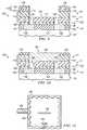
- FIG. 1shows a perspective view of a hybrid dielectric stack that will be patterned using a dual damascene method in accordance with an embodiment of the present invention, wherein the insulating layer to be patterned comprises a bi-layer of two different dielectric materials;
- FIG. 2is a flow chart for patterning a semiconductor device using the dual damascene method described herein;
- FIGS. 3 through 10show cross-sectional views of a semiconductor device at various stages of manufacturing in accordance with a dual damascene patterning method of an embodiment of the present invention.
- FIG. 11shows a chamber for processing semiconductor wafers in which polymers deposited on the chamber walls during the etching of inorganic material layers are cleaned or removed in-situ while a semiconductor wafer remains in the wafer in accordance with an embodiment of the present invention.
- FIG. 1shows a perspective view of a dielectric stack 100 in which a dual damascene structure will be fabricated in accordance with an embodiment of the present invention, wherein an insulating layer 110 to be patterned using a dual damascene process comprises a bi-layer of dielectric materials 112 and 114 .
- a first insulating layer 104which may comprise silicon dioxide or low-dielectric constant materials, for example, is deposited over a workpiece 102 .
- the workpiecemay include a semiconductor substrate comprising silicon or other semiconductor materials covered by an insulating layer, for example.
- the workpiecemay also include other active components or circuits, not shown.
- the workpiecemay comprise silicon oxide over single-crystal silicon, for example.
- the workpiecemay include other conductive layers or other semiconductor elements, e.g. transistors, diodes, etc. Compound semiconductors, GaAs, InP, Si/Ge, or SiC, as examples, may be used in place of silicon.
- a plurality of first conductive lines 106are formed in the first insulating layer 104 , for example, in a single damascene process.
- the first conductive lines 106may be formed using a subtractive etch process, followed by depositing the first insulating layer 104 over the patterned first conductive lines 106 , for example.
- the first conductive lines 106may comprise copper, a copper alloy, or other conductive materials, for example, and may include a liner formed over the patterned first insulating layer 104 to prevent diffusion of a metal such as copper into the first insulating layer 104 , for example, not shown.
- the thickness of the first conductive lines 106 and the first insulating layer 104may range from about 500 to 3000 Angstroms, as an example.
- the first conductive lines 106may be formed in a first metallization layer M1 of the semiconductor device, for example.
- a cap layer 108is deposited over the patterned first insulating layer 104 and the first conductive lines 106 .
- the cap layer 108comprises a copper cap that preferably functions as both a copper barrier, to prevent copper from diffusing or migrating into subsequently formed insulating layers (such as 112 ), and as an oxygen barrier, to prevent exposing the copper conductive lines 106 to oxygen in subsequent deposition and etch processes, which can cause corrosion.
- the cap layer 108preferably comprises silicon nitride (Si x N y ) or nitrogen-doped silicon carbide (N—SiC x ), as examples, although alternatively, the cap layer 108 may also comprise other insulating materials, for example.
- the cap layermay alternatively comprise SiC x , SiC x H y , SiCOH x , SiC x N y H z or SiN x H y , as examples.
- the material of the cap layer 108is selected to have a transparent effect on unit processes such as RIE.
- RIEunit processes
- a similar etch chemistrymay be used to etch either Si 3 N 4 or N—SiC x ; thus, these two materials may be used interchangeably in embodiments of the present invention without impacting the entire processing flow of the structure 100 .
- the cap layermay comprise a thickness of about 150 to 500 Angstroms, for example.
- An optional adhesion film 116may be formed on a top surface of the cap layer 108 .
- the adhesion film 116functions as an adhesion promoter for subsequently deposited first dielectric material 112 .
- the adhesion film 116may comprise AP6000TM manufactured by Dow Chemical Company or HOSP-BESTTM manufactured by Honeywell, Inc., as examples, although the adhesion film 116 may alternatively comprise other adhesion promoting materials.
- the adhesion film 116may be deposited by CVD or a spin-on process, as examples.
- the adhesion film 116may comprise a thickness of less than about 100 Angstroms, as an example.
- a second insulating layer 110 formed over the cap layer 108comprises a bi-layer including a first dielectric material 112 and a second dielectric material 114 , wherein the second dielectric material 114 preferably is etchable selective to the first dielectric material 112 in a dual damascene patterning process.
- a first dielectric material 112is deposited over the cap layer 108 or optional adhesion film 116 .
- the first dielectric material 112preferably comprises an inorganic dielectric material such as SiO 2 , undoped silicate glass (USG), fluorinated silicon glass (FSG), fluorinated tetraethoxysilate (FTEOS), SiCOH, or porous-SiCOH, as examples.
- the first dielectric material 112may be spun-on, or may be deposited by CVD, as examples.
- the cap layer 108may be treated with a plasma pre-treatment of the cap layer 108 prior to the CVD process.
- the plasma pre-treatmentexcites the surface of the cap layer 108 so that the CVD dielectric material 112 will deposit onto a dangling bond attraction.
- the first dielectric material 112may comprise a thickness of about 500 to 3000 Angstroms, for example.
- the first dielectric material 112comprises the portion of the second insulating layer 110 in which vias will be formed, in a dual damascene method.
- the first dielectric material 112comprises a via dielectric material or via insulating layer.
- the first conductive lines 106comprise copper
- the first dielectric material 114comprises a material having a coefficient of thermal expansion (CTE) that is close to the CTE of copper, or the CTE of the first conductive lines 106 , to prevent shearing or breaks in the electrical connection of the via to underlying first conductive lines over temperature-induced stress.
- CTEcoefficient of thermal expansion
- the first dielectric materialpreferably comprises a material having a low dielectric constant (e.g., having a dielectric constant k of 4.0 or less).
- a low dielectric constante.g., having a dielectric constant k of 4.0 or less.
- SiO 2typically has a k of about 4.0
- FSGtypically has a k of about 3.6
- FTEOStypically has a k of about 3.5
- SiCOHtypically has a k range of about 2.6-3.3
- porous-SiCOHtypically has a k range of less than 3.0.
- each material listed abovemay be etched by similar etch chemistries.
- a RIE using a fluorocarbon-based chemistryCH x F y
- CH x F yfluorocarbon-based chemistry
- An optional adhesion film 113may be formed on a top surface of the first dielectric material 112 .
- the adhesion film 113functions as an adhesion promoter for subsequently deposited second dielectric material 114 .
- the adhesion film 113may comprise AP6000TM manufactured by Dow Chemical Company or HOSP-BESTTM manufactured by Honeywell, Inc., as examples, although the adhesion film 113 may alternatively comprise other adhesion promoting materials.
- the adhesion film 113may be deposited by CVD or a spin-on process, as examples.
- the adhesion film 113may comprise a thickness of less than about 100 Angstroms, as an example.
- the second insulating layer 110includes a second dielectric material 114 deposited over the first dielectric material 112 .
- the second dielectric material 114preferably comprises an organic dielectric material such as SiLKTM or porous-SiLKTM manufactured by Dow Chemical Company, as examples.
- the second dielectric material 114may be spun-on, or may be deposited by CVD, as examples.
- the second dielectric material 114may comprise a thickness of about 500 to 3000 Angstroms, for example.
- the CTE of the second dielectric material 114does not have to closely match the CTE of the first conductive lines. Therefore, an organic material can be used.
- the second dielectric material 114preferably comprises a low-k dielectric material.
- SiLKTMtypically has a k of about 2.6 and porous-SiLKTM typically has a k of less than about 2.4.
- the etch process for the second dielectric material 114typically comprises a RIE using N 2 H 2 or N 2 O 2 plasmas, as examples. Because these etch chemistries do not remove or etch the first dielectric material 112 , a natural etch stop on the first dielectric material 112 is created. This allows scaling the RIE processes to smaller dimensions, because over-etching the second dielectric material 114 will not affect the first dielectric material 112 .
- the organic materials that may be used for the second dielectric material 114are typically etched with strip-type chemistries similar to the plasma strip processes used to remove photoresist, for example.
- the inorganic materials of the first dielectric material 112typically are etched with a fluoropolymer-based chemistry. Therefore, the etch processes and materials provide a natural etch step so that the etching of the second dielectric material 114 stops when the first dielectric material 112 is reached. End-pointing of the etch processes is made easier, and over-etching into the first dielectric material 112 is made possible because of the high etch selectivity of the second dielectric material 114 and the first dielectric material 112 . Therefore, a timed etch need not be relied upon to etch a second pattern, e.g., for conductive lines, in the second dielectric material 114 .
- the first dielectric material 112may comprise an organic dielectric material
- the second dielectric material 114comprises an inorganic dielectric material such as the organic and inorganic dielectric materials listed as examples, above.
- one of the first dielectric material 112 or second dielectric material 114comprises an organic dielectric material
- the other of the second dielectric material 114 or first dielectric material 112comprises an inorganic dielectric material.
- a hard mask 118is deposited over the second dielectric material 114 .
- the hard mask 118preferably comprises a tri-layer and may alternatively comprise two or more mask layers, for example.
- the multi-layered hard mask stack 118provides etch profile control and selectivity, acts as a CMP-stop and a barrier to prevent photoresist poisoning, and provides an enhanced lithographic process window for the depth of focus, to be described further herein.
- the thickness of the hard mask 118preferably may be tuned to the required CMP stop thickness (for the CMP process that will be used to remove excess conductive material from the top surface of the second dielectric material 114 after the damascene structure is filled, to be described further herein).
- the hard mask 118preferably comprises a first mask layer 120 , a second mask layer 126 formed over the first mask layer 120 , and a third mask layer 128 formed over the second mask layer 126 .
- the thickness of the mask layers 120 , 126 and 128may be altered to attain a CMP stop without sacrificing any material properties of the mask layers 120 , 126 or 128 in accordance with an embodiment of the present invention.
- the hard mask 118preferably comprises a first mask layer 120 comprising silicon carbide (SiC x ).
- the first mask layer 120in one embodiment comprises a first layer of SiC x (such as BLOkTM manufactured by Applied Materials) and a second layer of nitrogen-doped SiC x or N—SiC x (such as n-BLOkTM manufactured by Applied Materials) formed over the first layer of SiC x .
- the SiC x layermay comprise a thickness of between about 350 to 1000 Angstroms, and the N—SiC x layer may comprise a thickness of about 500 Angstroms or less, as examples.
- the first mask layer 120comprises a unitary low-k hard mask material that also serves as a CMP-stop material, comprising a material such as SiC x H y , SiCOH x , SiC x N y H z or SiN x H y , as examples.
- the low-k unitary hard maskmay comprise a thickness of between about 100 Angstroms to 1000 Angstroms, as example.
- the first mask layer 120provides a tunable CMP-stop window and enhances the RIE process window by eliminating micro-masking effects.
- the hard mask 118preferably comprises a second mask layer 126 disposed over the first mask layer 120 .
- the second mask layer 126preferably comprises Si 3 N 4 or SiO 2 , as examples.
- the second mask layer 126is preferably deposited by CVD and may comprise a thickness of about 150 to 500 Angstroms, for example.
- the second mask layer 126protects the underlying films 124 , 122 , 114 , and 112 from photoresist rework-induced damage. Photoresist rework may be required when trying to print a pattern. If there is misalignment after patterning the photoresist, the photoresist is removed, and then a fresh layer of photoresist is deposited and the patterning process is repeated, to attempt to obtain a better alignment.
- the strip processes usedmay comprise O 2 plasma, N 2 plasma, or H 2 plasma, as examples.
- the second mask layer 126prevents damage to the second dielectric material 114 and first dielectric material 112 from the plasma strip processes during
- the hard mask 118includes a third mask layer 128 disposed over the second mask layer 126 .
- the third mask layer 128preferably comprises a refractory metal nitride, such as TaN x as an example, although other materials may be used.
- the third mask layer 128may be deposited by CVD for example, and may comprise a thickness of 300 Angstroms or less.
- the third mask layer 128provides an improved depth of focus window for the lithography processes of the dual damascene structure 100 .
- the third mask layer 128in combination with the second mask layer 126 , prevents photoresist poisoning of subsequently-deposited photoresist 132 .
- the third mask layer 128also provides a higher etch selectivity to the organic and inorganic dielectric material (e.g. dielectric materials 112 and 114 ) etch processes. For example, a fluorocarbon-based etch affects TaN very slowly.
- the third mask layer 128functions as a line template in the present partial-via dual damascene patterning process.
- a photoresist(not shown in FIG. 1 ) is deposited over the third mask layer 128 , and the photoresist is patterned with a pattern 134 for second conductive lines that will be formed in the second dielectric material 114 , in a second metallization (M2) layer.
- the second conductive line pattern 134is transferred to the third mask layer 128 , using photolithography, as shown (e.g. by etching the third mask layer 128 using the patterned photoresist as a mask). Note that a top portion, e.g., less than about 100 Angstroms, of the second mask layer 126 may be removed while transferring the second conductive line pattern 134 to the third mask layer 128 , as shown.
- the combination of the third mask layer 128 and second mask layer 126prevents photoresist poisoning which typically would present a problem when SiCOH type materials are used for an insulating material.
- both the first dielectric material 112 and the second dielectric material 114are separated from the photoresist 132 by the multi-layer hard mask 118 . Therefore, if SiCOH-type materials are used for either the first dielectric material 112 or the second dielectric material 114 , photoresist poisoning does not occur, in accordance with embodiments of the present invention.
- An antireflective coating (ARC) 130is deposited over the hard mask 118 , as shown in FIG. 1 .
- the ARC 130comprises an organic or inorganic ARC commonly used to prevent reflection during a lithography process, and comprises a thickness of about 500 to 1500 Angstroms, for example.
- a photoresist 132is deposited over the ARC 130 .
- the photoresist 132is patterned with the pattern for vias 136 , as shown.
- the via pattern 136will be transferred to the first dielectric material 112 of the second insulating layer 110
- the second conductive line pattern 134will be transferred to the second dielectric material 114 of the second insulating layer 110 , shown and described herein with reference to FIGS. 3-9 .
- FIG. 2is a flow chart 140 for patterning a semiconductor device 100 using the dual damascene method described herein.
- FIGS. 3 through 10show cross-sectional views of a semiconductor device 100 at various stages of manufacturing in accordance with an embodiment of the present invention. The formation of a dual damascene structure in accordance with a preferred embodiment of the present invention by patterning the various layers of the dual damascene stack 100 shown in FIG. 1 will next be described, with reference to the flow chart in FIG. 2 and FIGS. 3-10 .
- FIG. 3shows a cross-sectional view of the dual damascene structure 100 shown in FIG. 1 .
- the second conductive line pattern 134has been formed in the third mask layer 128 of the hard mask.
- the via pattern 136has been formed in the photoresist 132 .
- the semiconductor deviceis subjected to a “via mask open” step 142 ( FIG. 2 ), as shown in FIG. 4 .
- the via mask open step 142preferably comprises a non-selective etch of the ARC 130 and all layers 128 , 126 and 120 of the hard mask 118 , for example.
- a top portion of the second dielectric material 114may be removed during the via mask open step, as shown in phantom. Note that a top portion of the photoresist 132 may also be removed during the via mask open.
- An advantage of using a non-selective etch for the via mask openis that any misalignment (e.g. by a distance d at 160 in FIG. 3 ) of the conductive line pattern 134 is opened (e.g., etched away) and removed, as shown in FIG. 4 .
- Another advantage of using a non-selective etch for the via mask openis that striations of the sidewalls of the vias may be prevented or minimized. Striations can cause star-shaped vias (rather than round vias, as is often desired), which can lead to shorting of adjacent vias in subsequent processing steps.
- the via mask openmay comprise a single step process, stopping in the second dielectric material 114 , or alternatively it may comprise a two step process with selectivity to the first mask layer 120 in the first step, and a first mask layer 120 only etch as part of the second step, for example.
- the etch chemistry of the via mask opencomprises O 2 gas with a flow rate ranging from about 10 to 100 standard cubic centimeters per minute (sccm), CF 4 gas with a flow rate ranging from about 10 to 200 sccm, and CH 2 F 2 gas with a flow rate ranging from about 0 to 50 sccm diluted in an inert gas such as Ar for about 10 seconds to 2 minutes, for example.
- the pressure for the via mask openmay range from about 20 to 300 mTorr, with an electrode plasma power density ranging from about 1 W/cm 2 to 10 W/cm 2 , and the bias power density ranging from about 0.1 W/cm 2 to 10 W/cm 2 .
- other etch chemistries, pressures, power density levels and timesmay be used for the via mask open, for example.
- the next processing stepcomprises a partial via step 144 ( FIG. 2 ) as shown in FIG. 5 .
- the via pattern 136 from the photoresist 132is transferred to the second dielectric material 114 or M2 metallization level of the second insulating layer 110 .
- exposed portions of the second dielectric material 114are etched while portions of the second dielectric material 114 protected by the hard mask 118 are not etched.
- the photoresistis preferably simultaneously removed from the top surface of the wafer, as shown in FIG. 5 .
- the partial via etchmay be endpointed so that the etch stops when the photoresist 132 is completely removed, for example.
- the partial via stepis preferably selective to the third mask layer 128 , the second mask layer 126 , and the first dielectric material 112 , in one embodiment.
- the etch chemistry for the partial via stepin one embodiment comprises N 2 gas with a flow rate ranging from about 100 to 1000 sccm, O 2 gas with a flow rate ranging from about 0 to 50 sccm, and H 2 gas with a flow rate ranging from about 0 to 500 sccm for about 15 seconds to 2 minutes, as an example.
- the pressure regimemay range from about 20 to 300 mTorr, with an electrode source power density ranging from about 1 W/cm 2 to 10 W/cm 2 , and a bias power density of about 2 W/cm 2 or less, as examples.
- other etch chemistries, pressures, power density levels and timesmay be used for the partial via step, for example.
- the partial via stepis optimized to ensure complete removal of all of the exposed second dielectric material 114 and photoresist 132 , while not producing sputter damage of the underlying first dielectric material 112 .
- Excessive overetch in this stepcan lead to the deposition of oxide on via walls which can affect via diameter and/or affect device reliability and performance.
- the overetch component in the partial via stepmay range from about 0% to 200% of the time required to clear the second dielectric material 114 and photoresist 132 , as an example.
- the next processing stepcomprises a trough open step 146 , ( FIG. 2 ) as shown in FIG. 6 .
- the purpose of this stepis to begin the transfer of the conductive line pattern 134 of the third mask layer 128 of the hard mask 118 .
- the remaining portions of the third mask layer 128are used as a mask to remove the second mask layer 126 and first mask layer 120 in the conductive line pattern 134 . Therefore, the trough open etch process is preferably selective to the third mask layer 128 .
- a top portion of the first dielectric material 112may be removed in the trough open step, as shown in phantom in FIG. 6 at 162 .
- Preferably, in the trough open etchall traces of the first mask layer are removed, while maintaining a high degree of selectivity to underlying second dielectric material 114 .
- the trough open stepcomprises an etch chemistry of O 2 gas with a flow rate ranging from about 10 to 50 sccm, CF 4 gas with a flow rate ranging from about 0 to 50 sccm, and CH 2 F 2 gas with a flow rate of about 50 sccm or less, diluted in an inert gas such as Ar for about 10 seconds to 1 minute, for example.
- the pressure regimemay range from about 50 to 150 mTorr, with an electrode power density ranging from about 1 W/cm 2 to 10 W/cm 2 , and a bias power density of about 2 W/cm 2 or less, as examples.
- other etch chemistries, pressures, power density levels and timesmay be used for the trough open step, for example.
- the next processing stepcomprises an oxide via etch step 148 ( FIG. 2 ), as shown in FIG. 7 .
- the via pattern 136 as defined in the partial via stepis transferred through the first dielectric material 112 (which may comprise oxide) of the V1 level.
- the via etch stepis preferably selective to the hard mask 118 and the second dielectric material 114 that is exposed in the trough areas at the sidewalls of the patterns 134 and 136 .
- the via etch stepis also preferably selective to the underlying cap layer 108 , which functions as an etch stop layer and diffusion barrier.
- An etch chemistry for the oxide via etch step in one embodimentcomprises O 2 gas with a flow rate ranging from about 10 to 50 sccm, CF 4 gas with a flow rate ranging from about 5 to 50 sccm, CO gas with flow rate of about 200 sccm or less, C 4 F 6 gas with a flow rate ranging from about 1 to 20 sccm, diluted in an inert gas such as Ar for about 10 seconds to 2 minutes, for example.
- the pressure regimemay range from about 30 to 100 mTorr, with an electrode plasma power density and bias power density of about 10 W/cm 2 or less, as examples.
- other etch chemistries, pressures, power density levels and timesmay be used for the oxide via etch step, for example.
- the oxide via etch stepmay be heavily polymerizing, forming polymers 184 on the interior surfaces of the processing chamber 180 for the semiconductor device 100 , as shown in FIG. 11 .
- the semiconductor device 100would result in polymers being removed from the chamber walls and forming aggressive reactant species that would chemically attack the hard mask 118 , which would degrade the fabrication process and lead to device failures.
- the processing chamberis cleaned while the wafer remains in the chamber (the in-situ chamber clean step 150 of FIG. 2 ), or the wafer is moved to a clean second processing chamber (step 152 of FIG. 2 ).
- the in-situ chamber cleaning processis a method of cleaning a chamber 180 that has been used to etch inorganic materials in semiconductor device fabrication, wherein the chamber has polymer build-up 184 on the interior walls thereof.
- the methodincludes, without removing a semiconductor wafer 182 that has been processed in the chamber 180 , introducing a plasma cleaning gas 186 into the chamber 180 to remove the polymer build-up 184 on the chamber walls without etching any material layers of the semiconductor wafer 182 .
- the plasma cleaning gas 186comprises a gas comprising O 2 gas diluted in Ar, He or N 2 .
- the O 2 concentrationmay comprise about 1% to 20% of the gas flow ratio, for example.
- the plasma cleaning gas 186may comprise other chemistries, for example.
- the methodmay further include applying power only to an electrode 188 in the chamber during cleaning, and not biasing the wafer during the cleaning method.
- the plasma electrode power density appliedmay comprise about 0.1 W/cm 2 to 10 W/cm 2 at a pressure of about 50 mTorr to 500 mTorr, for example.
- a hard mask(such as hard mask 118 of FIG. 1 ) formed on the semiconductor wafer 182 is not etched or removed during the cleaning method. In the cleaning process, any CF species that have formed on the interior walls of the chamber are converted to CN, CO or HF, as examples, which are then pumped out of the chamber (not shown).
- a trough etch step 153( FIG. 2 ) is then performed, as shown in FIG. 8 .
- the second dielectric material 114 remaining in the trough or conductive line pattern 134is selectively etched, with selectivity to the hard mask 118 , the cap layer 108 and the first dielectric material 112 .
- the hard mask 118 , cap layer 108 , and first dielectric material 112 structuresare defined in such a way as to ensure conductive line level dimensional control by maintaining a high degree of selectivity to the first conductive lines 106 which function as an etch stop layer.
- the degree of selectivityis such that the resulting etched structure is free of “grass” and other organic/inorganic residues, which could negatively affect device reliability performance.
- the trough etch stepmay comprise a single etch step or may comprise two or more etch steps.
- the trough etch stepcomprises an etch chemistry of N 2 gas with a flow rate ranging from about 100 to 1000 sccm, O 2 gas with a flow rate of about 50 sccm or less, H 2 gas with a flow rate of about 500 sccm or less for about 10 seconds to 2 minutes, for example.
- the pressure regimemay range from about 20 to 150 mTorr, with an electrode plasma power density ranging from about 1 W/cm 2 to 10 W/cm 2 , and a bias power density of about 2 W/cm 2 or less, as examples.
- other etch chemistries, pressures, power density levels and timesmay be used for the trough etch step, for example.
- the next processing stepcomprises a finish etch step 154 ( FIG. 2 ), as shown in FIG. 9 , in which the cap layer 108 is opened at the bottom of the via pattern 136 .
- the finish etchpreferably comprises an etch selective to the hard mask 118 and the exposed first dielectric material 112 .
- the finish etchmay comprise O 2 gas with flow rate of about 50 sccm or less, CF 4 gas with flow rate of about 50 sccm or less, N 2 gas with a flow rate of about 300 sccm or less, CHF 3 gas with flow rate of about 30 sccm or less, and CH 2 F 2 gas with flow rate of about 40 sccm or less, diluted in an inert gas such as Ar, for about 5 seconds to 30 seconds, as an example.
- the pressure regimemay range from about 50 to 150 mTorr, with an electrode plasma power density ranging from about 1 W/cm 2 to 10 W/cm 2 , and a bias power density of about 2 W/cm 2 or less, as examples.
- other etch chemistries, pressures, power and timesmay be used for the finish etch step, for example.
- a de-fluorination clean step 156( FIG. 2 ) is also shown in FIG. 9 .
- the de-fluorination clean stepany fluorinated organic species which may be absorbed to the wafer, conductive line pattern 134 sidewalls or via pattern 136 sidewalls are removed using a reducing plasma, for example.
- the etch chemistry for the de-fluorination clean stepcomprises N 2 gas with a flow rate ranging from about 100 to 1000 sccm and H 2 gas with a flow rate of about 500 sccm or less for about 5 to 30 seconds, as an example.
- the pressure regimemay range from about 100 to 150 mTorr, with an electrode plasma power density ranging from about 1 W/cm 2 to 10 W/cm 2 , and a bias power density ranging from about 2 W/cm 2 or less, as examples.
- electrode plasma power densityranging from about 1 W/cm 2 to 10 W/cm 2
- bias power densityranging from about 2 W/cm 2 or less
- other etch chemistries, pressures, power and timesmay be used for the de-fluorination clean step, for example.
- a conductive material 164is deposited over the patterned second dielectric material 114 and the patterned first dielectric material 112 , as shown in FIG. 10 .
- the conductive material 164is removed from the top surface of the second dielectric material, e.g., using a CMP process, leaving conductive material 164 in the via pattern 136 and conductive line pattern 134 to form vias 166 and conductive lines 168 , respectively.
- a portion of the hard mask 118may remain residing over the top surface of the second dielectric material 114 of the second insulating layer 110 after the CMP process.
- Advantages of embodiments of the present inventioninclude providing an insulating layer 110 for a dual damascene process and structure, in which the different materials of the dielectric layers 112 and 114 creates a natural etch stop. This results in improved RIE write profiles and the ability to form features such as vias 166 with substantially vertical sidewalls, rather than being tapered as in prior art via formation. Conductive lines 168 having smaller critical dimensions may be obtained with the improved manufacturing control provided by the bi-layer insulating layer 110 . The thickness and materials of the bottom mask layer 120 of the hard mask 118 are tunable for a particular application as a CMP stop layer. Photoresist poisoning during a dual damascene etch process is prevented with the use of embodiments of the present invention. The materials used in the various layers of the structure may be changed without impacting or affecting the remainder of the stack 100 .
- Advantages of the method of forming a dual damascene structure 100include providing a dual damascene etch process that enables a dual damascene integration scheme. Modifications may be made to a specific component of the etch process to account for a material change in the via patterning etch process or the line patterning etch process, which does not affect the remainder of the etch scheme. The need for a timed etch to pattern the shallower conductive line pattern 134 , which is difficult to control, is eliminated.
- the dual damascene processmay be completed in a single chamber or alternatively in multiple chambers. A novel method of cleaning a chamber while the wafer remains in the chamber is also disclosed.
Landscapes
- Engineering & Computer Science (AREA)
- Physics & Mathematics (AREA)
- Manufacturing & Machinery (AREA)
- Computer Hardware Design (AREA)
- Power Engineering (AREA)
- Microelectronics & Electronic Packaging (AREA)
- Condensed Matter Physics & Semiconductors (AREA)
- General Physics & Mathematics (AREA)
- Chemical & Material Sciences (AREA)
- Chemical Kinetics & Catalysis (AREA)
- General Chemical & Material Sciences (AREA)
- Plasma & Fusion (AREA)
- Inorganic Chemistry (AREA)
- Health & Medical Sciences (AREA)
- Epidemiology (AREA)
- Public Health (AREA)
- Analytical Chemistry (AREA)
- Internal Circuitry In Semiconductor Integrated Circuit Devices (AREA)
Abstract
Description
- This application relates to the following co-pending and commonly assigned patent applications: Ser. No. ______, filed concurrently herewith, entitled Dual Damascene Structure and Method, which application is hereby incorporated herein by reference.
- The present invention relates generally to the fabrication of semiconductor devices, and more particularly to the fabrication of a dual damascene structure.
- Semiconductor devices are fabricated by sequentially depositing insulating (or dielectric) layers, conductive layers and semiconductive layers of material over a semiconductor substrate, and patterning the various layers using lithography to form circuit components and elements thereon. A common conductive material used in the past for conductive lines was aluminum, which can be directly etched. For example, a layer of aluminum or aluminum alloy is deposited, a photoresist layer is deposited over the aluminum, the photoresist is patterned and developed, and the photoresist is used as a mask while exposed areas of the aluminum layer are etched away.
- There is a trend in the semiconductor industry towards the use of copper for conductive lines and metallization layers. Copper introduces new challenges in semiconductor device fabrication. While copper is more conductive than aluminum, which is an advantage, it has a tendency to diffuse through dielectric layers, causing shorts and device failures. Therefore, liners are used to prevent this diffusion. Also, copper cannot be directly etched, particularly in small minimum feature sizes, which leads to the use of damascene methods to form copper conductive lines.
- In a damascene method of forming conductive lines, an insulating layer is deposited over a semiconductor substrate, and the insulating layer is patterned, e.g. by depositing a photoresist, patterning and developing the photoresist, and using the photoresist as a mask for the insulating layer while exposed portions of the insulating layer are etched away. A conductive material (such as copper) is deposited over the patterned insulating layer, e.g. by chemical vapor deposition (CVD), electroplating or electro-less plating, or other deposition methods. The semiconductor substrate is chemically-mechanically polished (CMP) to remove excess conductive material from over the top surface of the insulating layer, leaving conductive lines or regions formed in the insulating layer.
- If one pattern is formed in the insulating layer, the process is referred to as a single damascene process. However, two patterns may also be formed in the insulating layer, with one pattern typically being etched deeper into the insulating layer than the other pattern. The two pattern process is referred to in the art as a dual damascene process. A dual damascene process may be used to form a first layer of vias to connect to underlying conductive lines or elements, for example, and a second layer of conductive lines or regions may be formed over the vias.
- In the prior art, typically either the vias are first patterned in the insulating layer through the entire thickness of the insulating layer, and then the conductive lines are patterned in a top portion of the insulating layer, often referred to as a “via-first” dual damascene patterning method. Or, the conductive lines may alternatively be patterned in a top portion of the insulating layer first, followed by the patterning of the vias through the entire thickness of the insulating layer, called a “line-first” dual damascene method.
- As semiconductor device sizes decrease and the minimum feature size of the electrical components and conductive lines decrease, patterning an insulating layer in a dual damascene process becomes more and more difficult. In a dual damascene patterning process, one of the patterning steps etches through the entire thickness of the insulating layer (forming the vias, for example), and the other patterning step etches only through part of the insulating layer (forming the conductive lines), using a timed etch, for example. There is a trend in the semiconductor industry towards the use of low-dielectric constant (low-k) dielectric materials, particularly used in conjunction with copper conductive lines, to reduce the RC time delay of the conductive lines. Some low-k dielectric materials are porous and/or etch very quickly, and it can be difficult to adequately control the etch process, particularly in a dual damascene structure and process.
- Another problem in dual damascene patterning is photoresist poisoning, which can occur during a patterning process when etch chemistries containing nitrogen are used to pattern insulating layers comprising SiCOH-type (materials containing silicon, carbon, oxygen, and/or hydrogen) materials, which are often used as insulators. The nitrogen-containing etch chemistries, in conjunction with the SiCOH-type materials, liberate amines that can interact with or migrate into the photoresist during a subsequent lithography step. Photoresist poisoning causes depth of focus problems and/or delamination of the photoresist, resulting in loss of control of the critical dimensions and the inability to print, which leads to device failures and decreased yields. Photoresist poisoning tends to be a problem in via-first dual damascene patterning methods and also in line-first dual damascene patterning methods because the subsequent application of photoresist is exposed to the amines generated during the previous etch process.
- Therefore, what is needed in the art is a dual damascene structure and method with improved control of patterning a damascene structure that avoids photoresist poisoning.
- Embodiments of the present invention solve these problems by providing a novel partial-via dual damascene structure and method. The dual damascene insulating layer includes a first insulating material having a first etch selectivity and a second insulating material having a second etch selectivity. Because the first etch selectivity is different from the second etch selectivity, the first and second insulating materials may be etched selective to one another, providing improved control for the dual damascene etch process.
- In accordance with a preferred embodiment of the present invention, a method of fabricating a semiconductor device includes providing a workpiece, disposing a first dielectric material over the workpiece, and disposing a second dielectric material over the first dielectric material. The second dielectric material comprises a different material than the first dielectric material, wherein the first dielectric material and the second dielectric material comprise a first insulating layer. A first pattern is formed in the first dielectric material and a second pattern is formed in the second dielectric material, the second pattern being different from the first pattern.
- In accordance with another preferred embodiment of the present invention, a method of fabricating a semiconductor device includes providing a workpiece, forming a first insulating layer over the workpiece, forming a plurality of first conductive lines in the first insulating layer, disposing a first dielectric material over the first insulating layer, and disposing a second dielectric material over the first dielectric material. The second dielectric material comprises a different material than the first dielectric material, and the first dielectric material and the second dielectric material comprise a second insulating layer. The method includes forming a first pattern in the first dielectric material and a second pattern in the second dielectric material, the second pattern being different from the first pattern. A conductive material is deposited over the patterned second dielectric material and the patterned first dielectric material. The conductive material is removed from the top surface of the second dielectric material to form a plurality of second conductive lines in the second pattern of the second dielectric material and a plurality of vias in the first pattern of the first dielectric material.
- Yet another preferred embodiment of the present invention is a method of cleaning a chamber that has been used to etch inorganic materials in semiconductor device fabrication, the chamber having polymer build-up on the interior walls thereof. The method includes introducing a plasma cleaning gas into the chamber to remove the polymer build-up on the chamber walls, without removing the semiconductor wafer that has been processed in the chamber and without etching a material layer of the semiconductor wafer.
- Advantages of preferred embodiments of the present invention include providing a dual damascene hybrid dielectric stack having natural etch stops and enhanced reactive ion etch (RIE) profiles. The bottom layer of the hard mask is tunable for a particular application as a chemical-mechanical polish (CMP) stop layer. Photoresist poisoning during a dual damascene etch process is prevented with the use of embodiments of the present invention. The materials used in the various layers of the structure may be changed without impacting or affecting the remainder of the stack. Vias with substantially vertical sidewalls and smaller critical dimensions are achievable using embodiments of the present invention.
- Advantages of a method of forming a dual damascene structure according to an embodiment of the present invention include providing a dual damascene etch process that enables a dual damascene integration scheme. Modifications may be made to a specific component of the etch process to account for a material change in the via patterning etch process or the line patterning etch process, which does not affect the remainder of the etch scheme. The need for a timed etch to pattern the shallower conductive line pattern, which is difficult to control, is eliminated. The dual damascene process may be completed in a single chamber or alternatively in multiple chambers. A novel method of cleaning a chamber while the wafer remains in the chamber is also disclosed.
- The foregoing has outlined rather broadly the features and technical advantages of embodiments of the present invention in order that the detailed description of the invention that follows may be better understood. Additional features and advantages of embodiments of the invention will be described hereinafter, which form the subject of the claims of the invention. It should be appreciated by those skilled in the art that the conception and specific embodiments disclosed may be readily utilized as a basis for modifying or designing other structures or processes for carrying out the same purposes of the present invention. It should also be realized by those skilled in the art that such equivalent constructions do not depart from the spirit and scope of the invention as set forth in the appended claims.
- For a more complete understanding of the present invention, and the advantages thereof, reference is now made to the following descriptions taken in conjunction with the accompanying drawings, in which:
FIG. 1 shows a perspective view of a hybrid dielectric stack that will be patterned using a dual damascene method in accordance with an embodiment of the present invention, wherein the insulating layer to be patterned comprises a bi-layer of two different dielectric materials;FIG. 2 is a flow chart for patterning a semiconductor device using the dual damascene method described herein;FIGS. 3 through 10 show cross-sectional views of a semiconductor device at various stages of manufacturing in accordance with a dual damascene patterning method of an embodiment of the present invention; andFIG. 11 shows a chamber for processing semiconductor wafers in which polymers deposited on the chamber walls during the etching of inorganic material layers are cleaned or removed in-situ while a semiconductor wafer remains in the wafer in accordance with an embodiment of the present invention.- Corresponding numerals and symbols in the different figures generally refer to corresponding parts unless otherwise indicated. The figures are drawn to clearly illustrate the relevant aspects of the preferred embodiments and are not necessarily drawn to scale.
- The making and using of the presently preferred embodiments are discussed in detail below. It should be appreciated, however, that the present invention provides many applicable inventive concepts that can be embodied in a wide variety of specific contexts. The specific embodiments discussed are merely illustrative of specific ways to make and use the invention, and do not limit the scope of the invention.
FIG. 1 shows a perspective view of adielectric stack 100 in which a dual damascene structure will be fabricated in accordance with an embodiment of the present invention, wherein an insulatinglayer 110 to be patterned using a dual damascene process comprises a bi-layer ofdielectric materials layer 104 which may comprise silicon dioxide or low-dielectric constant materials, for example, is deposited over aworkpiece 102. The workpiece may include a semiconductor substrate comprising silicon or other semiconductor materials covered by an insulating layer, for example. The workpiece may also include other active components or circuits, not shown. The workpiece may comprise silicon oxide over single-crystal silicon, for example. The workpiece may include other conductive layers or other semiconductor elements, e.g. transistors, diodes, etc. Compound semiconductors, GaAs, InP, Si/Ge, or SiC, as examples, may be used in place of silicon.- A plurality of first
conductive lines 106 are formed in the first insulatinglayer 104, for example, in a single damascene process. Alternatively, the firstconductive lines 106 may be formed using a subtractive etch process, followed by depositing the first insulatinglayer 104 over the patterned firstconductive lines 106, for example. The firstconductive lines 106 may comprise copper, a copper alloy, or other conductive materials, for example, and may include a liner formed over the patterned first insulatinglayer 104 to prevent diffusion of a metal such as copper into the first insulatinglayer 104, for example, not shown. The thickness of the firstconductive lines 106 and the first insulatinglayer 104 may range from about 500 to 3000 Angstroms, as an example. The firstconductive lines 106 may be formed in a first metallization layer M1 of the semiconductor device, for example. - A
cap layer 108 is deposited over the patterned first insulatinglayer 104 and the firstconductive lines 106. Thecap layer 108 comprises a copper cap that preferably functions as both a copper barrier, to prevent copper from diffusing or migrating into subsequently formed insulating layers (such as112), and as an oxygen barrier, to prevent exposing the copperconductive lines 106 to oxygen in subsequent deposition and etch processes, which can cause corrosion. Thecap layer 108 preferably comprises silicon nitride (SixNy) or nitrogen-doped silicon carbide (N—SiCx), as examples, although alternatively, thecap layer 108 may also comprise other insulating materials, for example. The cap layer may alternatively comprise SiCx, SiCxHy, SiCOHx, SiCxNyHzor SiNxHy, as examples. - Preferably, the material of the
cap layer 108 is selected to have a transparent effect on unit processes such as RIE. For example, from a RIE perspective, a similar etch chemistry may be used to etch either Si3N4or N—SiCx; thus, these two materials may be used interchangeably in embodiments of the present invention without impacting the entire processing flow of thestructure 100. The cap layer may comprise a thickness of about 150 to 500 Angstroms, for example. - An
optional adhesion film 116 may be formed on a top surface of thecap layer 108. Theadhesion film 116 functions as an adhesion promoter for subsequently deposited firstdielectric material 112. Theadhesion film 116 may comprise AP6000™ manufactured by Dow Chemical Company or HOSP-BEST™ manufactured by Honeywell, Inc., as examples, although theadhesion film 116 may alternatively comprise other adhesion promoting materials. Theadhesion film 116 may be deposited by CVD or a spin-on process, as examples. Theadhesion film 116 may comprise a thickness of less than about 100 Angstroms, as an example. - A second insulating
layer 110 formed over thecap layer 108 comprises a bi-layer including a firstdielectric material 112 and a seconddielectric material 114, wherein the seconddielectric material 114 preferably is etchable selective to the firstdielectric material 112 in a dual damascene patterning process. To form the second insulatinglayer 110, a firstdielectric material 112 is deposited over thecap layer 108 oroptional adhesion film 116. The firstdielectric material 112 preferably comprises an inorganic dielectric material such as SiO2, undoped silicate glass (USG), fluorinated silicon glass (FSG), fluorinated tetraethoxysilate (FTEOS), SiCOH, or porous-SiCOH, as examples. The firstdielectric material 112 may be spun-on, or may be deposited by CVD, as examples. In one embodiment, thecap layer 108 may be treated with a plasma pre-treatment of thecap layer 108 prior to the CVD process. The plasma pre-treatment excites the surface of thecap layer 108 so that theCVD dielectric material 112 will deposit onto a dangling bond attraction. The firstdielectric material 112 may comprise a thickness of about 500 to 3000 Angstroms, for example. - The first
dielectric material 112 comprises the portion of the second insulatinglayer 110 in which vias will be formed, in a dual damascene method. Thus, the firstdielectric material 112 comprises a via dielectric material or via insulating layer. If the firstconductive lines 106 comprise copper, preferably, the firstdielectric material 114 comprises a material having a coefficient of thermal expansion (CTE) that is close to the CTE of copper, or the CTE of the firstconductive lines 106, to prevent shearing or breaks in the electrical connection of the via to underlying first conductive lines over temperature-induced stress. - In one embodiment, the first dielectric material preferably comprises a material having a low dielectric constant (e.g., having a dielectric constant k of 4.0 or less). For example, SiO2typically has a k of about 4.0, FSG typically has a k of about 3.6, FTEOS typically has a k of about 3.5, SiCOH typically has a k range of about 2.6-3.3, and porous-SiCOH typically has a k range of less than 3.0.
- One advantage of these selections of materials for the first
dielectric material 112 is that typically, each material listed above may be etched by similar etch chemistries. For example, a RIE using a fluorocarbon-based chemistry (CHxFy) may be used to etch all of the possible materials that may be used for the firstdielectric material 112 described herein. This is advantageous in that these materials may be interchanged in the material stack without having to modify etch processing parameters of the dual damascene integration scheme. Also, in one embodiment, these materials are selected so that they may be etched selective to thecap layer 108. - An
optional adhesion film 113 may be formed on a top surface of the firstdielectric material 112. Theadhesion film 113 functions as an adhesion promoter for subsequently deposited seconddielectric material 114. Theadhesion film 113 may comprise AP6000™ manufactured by Dow Chemical Company or HOSP-BEST™ manufactured by Honeywell, Inc., as examples, although theadhesion film 113 may alternatively comprise other adhesion promoting materials. Theadhesion film 113 may be deposited by CVD or a spin-on process, as examples. Theadhesion film 113 may comprise a thickness of less than about 100 Angstroms, as an example. - The second
insulating layer 110 includes a seconddielectric material 114 deposited over the firstdielectric material 112. The seconddielectric material 114 preferably comprises an organic dielectric material such as SiLK™ or porous-SiLK™ manufactured by Dow Chemical Company, as examples. The seconddielectric material 114 may be spun-on, or may be deposited by CVD, as examples. The seconddielectric material 114 may comprise a thickness of about 500 to 3000 Angstroms, for example. - Advantageously, the CTE of the second
dielectric material 114 does not have to closely match the CTE of the first conductive lines. Therefore, an organic material can be used. The seconddielectric material 114 preferably comprises a low-k dielectric material. For example, SiLK™ typically has a k of about 2.6 and porous-SiLK™ typically has a k of less than about 2.4. - Another advantage of the materials listed that may be used for the second
dielectric material 114 is that etch chemistries used to etch the seconddielectric material 114 do not etch the firstdielectric material 112. For example, the etch process for the seconddielectric material 114 typically comprises a RIE using N2H2or N2O2plasmas, as examples. Because these etch chemistries do not remove or etch the firstdielectric material 112, a natural etch stop on the firstdielectric material 112 is created. This allows scaling the RIE processes to smaller dimensions, because over-etching the seconddielectric material 114 will not affect the firstdielectric material 112. - Advantageously, the organic materials that may be used for the second
dielectric material 114 are typically etched with strip-type chemistries similar to the plasma strip processes used to remove photoresist, for example. The inorganic materials of the firstdielectric material 112 typically are etched with a fluoropolymer-based chemistry. Therefore, the etch processes and materials provide a natural etch step so that the etching of the seconddielectric material 114 stops when the firstdielectric material 112 is reached. End-pointing of the etch processes is made easier, and over-etching into the firstdielectric material 112 is made possible because of the high etch selectivity of the seconddielectric material 114 and the firstdielectric material 112. Therefore, a timed etch need not be relied upon to etch a second pattern, e.g., for conductive lines, in the seconddielectric material 114. - In an alternative embodiment, the first
dielectric material 112 may comprise an organic dielectric material, and the seconddielectric material 114 comprises an inorganic dielectric material such as the organic and inorganic dielectric materials listed as examples, above. To achieve the etch selectivity between the first and seconddielectric materials dielectric material 112 or seconddielectric material 114 comprises an organic dielectric material, and the other of the seconddielectric material 114 or firstdielectric material 112 comprises an inorganic dielectric material. - A
hard mask 118 is deposited over the seconddielectric material 114. Thehard mask 118 preferably comprises a tri-layer and may alternatively comprise two or more mask layers, for example. The multi-layeredhard mask stack 118 provides etch profile control and selectivity, acts as a CMP-stop and a barrier to prevent photoresist poisoning, and provides an enhanced lithographic process window for the depth of focus, to be described further herein. The thickness of thehard mask 118 preferably may be tuned to the required CMP stop thickness (for the CMP process that will be used to remove excess conductive material from the top surface of the seconddielectric material 114 after the damascene structure is filled, to be described further herein). For example, thehard mask 118 preferably comprises afirst mask layer 120, asecond mask layer 126 formed over thefirst mask layer 120, and athird mask layer 128 formed over thesecond mask layer 126. The thickness of the mask layers120,126 and128 may be altered to attain a CMP stop without sacrificing any material properties of the mask layers120,126 or128 in accordance with an embodiment of the present invention. After the CMP process, it may be desirable to leave a portion of at least thefirst mask layer 120 disposed over the seconddielectric material 114, which may comprise a porous material, to prevent the ingress of water and CMP slurry into the pores of the seconddielectric material 114, for example. - The
hard mask 118 preferably comprises afirst mask layer 120 comprising silicon carbide (SiCx). Thefirst mask layer 120 in one embodiment comprises a first layer of SiCx(such as BLOk™ manufactured by Applied Materials) and a second layer of nitrogen-doped SiCxor N—SiCx(such as n-BLOk™ manufactured by Applied Materials) formed over the first layer of SiCx. The SiCxlayer may comprise a thickness of between about 350 to 1000 Angstroms, and the N—SiCxlayer may comprise a thickness of about 500 Angstroms or less, as examples. In another embodiment, thefirst mask layer 120 comprises a unitary low-k hard mask material that also serves as a CMP-stop material, comprising a material such as SiCxHy, SiCOHx, SiCxNyHzor SiNxHy, as examples. The low-k unitary hard mask may comprise a thickness of between about 100 Angstroms to 1000 Angstroms, as example. Thefirst mask layer 120 provides a tunable CMP-stop window and enhances the RIE process window by eliminating micro-masking effects. - The
hard mask 118 preferably comprises asecond mask layer 126 disposed over thefirst mask layer 120. Thesecond mask layer 126 preferably comprises Si3N4or SiO2, as examples. Thesecond mask layer 126 is preferably deposited by CVD and may comprise a thickness of about 150 to 500 Angstroms, for example. Thesecond mask layer 126 protects the underlyingfilms second mask layer 126 prevents damage to the seconddielectric material 114 and firstdielectric material 112 from the plasma strip processes during rework. - The
hard mask 118 includes athird mask layer 128 disposed over thesecond mask layer 126. Thethird mask layer 128 preferably comprises a refractory metal nitride, such as TaNxas an example, although other materials may be used. Thethird mask layer 128 may be deposited by CVD for example, and may comprise a thickness of 300 Angstroms or less. Thethird mask layer 128 provides an improved depth of focus window for the lithography processes of thedual damascene structure 100. Thethird mask layer 128, in combination with thesecond mask layer 126, prevents photoresist poisoning of subsequently-depositedphotoresist 132. Thethird mask layer 128 also provides a higher etch selectivity to the organic and inorganic dielectric material (e.g.dielectric materials 112 and114) etch processes. For example, a fluorocarbon-based etch affects TaN very slowly. - The
third mask layer 128 functions as a line template in the present partial-via dual damascene patterning process. In particular, a photoresist (not shown inFIG. 1 ) is deposited over thethird mask layer 128, and the photoresist is patterned with apattern 134 for second conductive lines that will be formed in the seconddielectric material 114, in a second metallization (M2) layer. The secondconductive line pattern 134 is transferred to thethird mask layer 128, using photolithography, as shown (e.g. by etching thethird mask layer 128 using the patterned photoresist as a mask). Note that a top portion, e.g., less than about 100 Angstroms, of thesecond mask layer 126 may be removed while transferring the secondconductive line pattern 134 to thethird mask layer 128, as shown. - In one embodiment, the combination of the
third mask layer 128 andsecond mask layer 126 prevents photoresist poisoning which typically would present a problem when SiCOH type materials are used for an insulating material. Advantageously, both the firstdielectric material 112 and the seconddielectric material 114 are separated from thephotoresist 132 by the multi-layerhard mask 118. Therefore, if SiCOH-type materials are used for either the firstdielectric material 112 or the seconddielectric material 114, photoresist poisoning does not occur, in accordance with embodiments of the present invention. - An antireflective coating (ARC)130 is deposited over the
hard mask 118, as shown inFIG. 1 . TheARC 130 comprises an organic or inorganic ARC commonly used to prevent reflection during a lithography process, and comprises a thickness of about 500 to 1500 Angstroms, for example. Aphotoresist 132 is deposited over theARC 130. Thephotoresist 132 is patterned with the pattern forvias 136, as shown. The viapattern 136 will be transferred to the firstdielectric material 112 of the second insulatinglayer 110, and the secondconductive line pattern 134 will be transferred to the seconddielectric material 114 of the second insulatinglayer 110, shown and described herein with reference toFIGS. 3-9 . FIG. 2 is aflow chart 140 for patterning asemiconductor device 100 using the dual damascene method described herein.FIGS. 3 through 10 show cross-sectional views of asemiconductor device 100 at various stages of manufacturing in accordance with an embodiment of the present invention. The formation of a dual damascene structure in accordance with a preferred embodiment of the present invention by patterning the various layers of the dualdamascene stack 100 shown inFIG. 1 will next be described, with reference to the flow chart inFIG. 2 andFIGS. 3-10 .- The process flow begins with the
dual damascene structure 100 ofFIG. 1 .FIG. 3 shows a cross-sectional view of thedual damascene structure 100 shown inFIG. 1 . The secondconductive line pattern 134 has been formed in thethird mask layer 128 of the hard mask. The viapattern 136 has been formed in thephotoresist 132. - The semiconductor device is subjected to a “via mask open” step142 (
FIG. 2 ), as shown inFIG. 4 . The via maskopen step 142 preferably comprises a non-selective etch of theARC 130 and alllayers hard mask 118, for example. Optionally, a top portion of the seconddielectric material 114 may be removed during the via mask open step, as shown in phantom. Note that a top portion of thephotoresist 132 may also be removed during the via mask open. - An advantage of using a non-selective etch for the via mask open is that any misalignment (e.g. by a distance d at160 in
FIG. 3 ) of theconductive line pattern 134 is opened (e.g., etched away) and removed, as shown inFIG. 4 . Another advantage of using a non-selective etch for the via mask open is that striations of the sidewalls of the vias may be prevented or minimized. Striations can cause star-shaped vias (rather than round vias, as is often desired), which can lead to shorting of adjacent vias in subsequent processing steps. - The via mask open may comprise a single step process, stopping in the second
dielectric material 114, or alternatively it may comprise a two step process with selectivity to thefirst mask layer 120 in the first step, and afirst mask layer 120 only etch as part of the second step, for example. - In one embodiment, the etch chemistry of the via mask open comprises O2gas with a flow rate ranging from about 10 to 100 standard cubic centimeters per minute (sccm), CF4gas with a flow rate ranging from about 10 to 200 sccm, and CH2F2gas with a flow rate ranging from about 0 to 50 sccm diluted in an inert gas such as Ar for about 10 seconds to 2 minutes, for example. The pressure for the via mask open may range from about 20 to 300 mTorr, with an electrode plasma power density ranging from about 1 W/cm2to 10 W/cm2, and the bias power density ranging from about 0.1 W/cm2to 10 W/cm2. Alternatively, other etch chemistries, pressures, power density levels and times may be used for the via mask open, for example.
- The next processing step comprises a partial via step144 (
FIG. 2 ) as shown inFIG. 5 . In the partial via step, the viapattern 136 from thephotoresist 132 is transferred to the seconddielectric material 114 or M2 metallization level of the second insulatinglayer 110. In particular, exposed portions of the seconddielectric material 114 are etched while portions of the seconddielectric material 114 protected by thehard mask 118 are not etched. In the partial via step, the photoresist is preferably simultaneously removed from the top surface of the wafer, as shown inFIG. 5 . The partial via etch may be endpointed so that the etch stops when thephotoresist 132 is completely removed, for example. Because the etchant chemistries do not etch the firstdielectric material 112, the etch stops on the firstdielectric material 112, and the etch may be continued until thephotoresist 132 is completely removed, leaving theconductive line pattern 134 of thehard mask 118 exposed. The partial via step is preferably selective to thethird mask layer 128, thesecond mask layer 126, and the firstdielectric material 112, in one embodiment. - The etch chemistry for the partial via step in one embodiment comprises N2gas with a flow rate ranging from about 100 to 1000 sccm, O2gas with a flow rate ranging from about 0 to 50 sccm, and H2gas with a flow rate ranging from about 0 to 500 sccm for about 15 seconds to 2 minutes, as an example. The pressure regime may range from about 20 to 300 mTorr, with an electrode source power density ranging from about 1 W/cm2to 10 W/cm2, and a bias power density of about 2 W/cm2or less, as examples. Alternatively, other etch chemistries, pressures, power density levels and times may be used for the partial via step, for example.
- Preferably, the partial via step is optimized to ensure complete removal of all of the exposed second
dielectric material 114 andphotoresist 132, while not producing sputter damage of the underlying firstdielectric material 112. Excessive overetch in this step can lead to the deposition of oxide on via walls which can affect via diameter and/or affect device reliability and performance. The overetch component in the partial via step may range from about 0% to 200% of the time required to clear the seconddielectric material 114 andphotoresist 132, as an example. - The next processing step comprises a trough
open step 146, (FIG. 2 ) as shown inFIG. 6 . The purpose of this step is to begin the transfer of theconductive line pattern 134 of thethird mask layer 128 of thehard mask 118. The remaining portions of thethird mask layer 128 are used as a mask to remove thesecond mask layer 126 andfirst mask layer 120 in theconductive line pattern 134. Therefore, the trough open etch process is preferably selective to thethird mask layer 128. Note that a top portion of the firstdielectric material 112 may be removed in the trough open step, as shown in phantom inFIG. 6 at162. Preferably, in the trough open etch, all traces of the first mask layer are removed, while maintaining a high degree of selectivity to underlying seconddielectric material 114. - In one embodiment, the trough open step comprises an etch chemistry of O2gas with a flow rate ranging from about 10 to 50 sccm, CF4gas with a flow rate ranging from about 0 to 50 sccm, and CH2F2gas with a flow rate of about 50 sccm or less, diluted in an inert gas such as Ar for about 10 seconds to 1 minute, for example. The pressure regime may range from about 50 to 150 mTorr, with an electrode power density ranging from about 1 W/cm2to 10 W/cm2, and a bias power density of about 2 W/cm2or less, as examples. Alternatively, other etch chemistries, pressures, power density levels and times may be used for the trough open step, for example.
- The next processing step comprises an oxide via etch step148 (
FIG. 2 ), as shown inFIG. 7 . In the oxide via etch step, the viapattern 136 as defined in the partial via step is transferred through the first dielectric material112 (which may comprise oxide) of the V1 level. The via etch step is preferably selective to thehard mask 118 and the seconddielectric material 114 that is exposed in the trough areas at the sidewalls of thepatterns underlying cap layer 108, which functions as an etch stop layer and diffusion barrier. - An etch chemistry for the oxide via etch step in one embodiment comprises O2gas with a flow rate ranging from about 10 to 50 sccm, CF4gas with a flow rate ranging from about 5 to 50 sccm, CO gas with flow rate of about 200 sccm or less, C4F6gas with a flow rate ranging from about 1 to 20 sccm, diluted in an inert gas such as Ar for about 10 seconds to 2 minutes, for example. The pressure regime may range from about 30 to 100 mTorr, with an electrode plasma power density and bias power density of about 10 W/cm2or less, as examples. Alternatively, other etch chemistries, pressures, power density levels and times may be used for the oxide via etch step, for example.
- The oxide via etch step may be heavily polymerizing, forming polymers184 on the interior surfaces of the
processing chamber 180 for thesemiconductor device 100, as shown inFIG. 11 . Continuing to process thesemiconductor device 100 would result in polymers being removed from the chamber walls and forming aggressive reactant species that would chemically attack thehard mask 118, which would degrade the fabrication process and lead to device failures. Thus, at this point in the manufacturing process flow, either the processing chamber is cleaned while the wafer remains in the chamber (the in-situ chamberclean step 150 ofFIG. 2 ), or the wafer is moved to a clean second processing chamber (step152 ofFIG. 2 ). - The novel in-situ chamber cleaning process of a semiconductor wafer in accordance with an embodiment of the present invention will next be described, with reference to
FIG. 11 . The in-situ chamber cleaning process is a method of cleaning achamber 180 that has been used to etch inorganic materials in semiconductor device fabrication, wherein the chamber has polymer build-up184 on the interior walls thereof. The method includes, without removing asemiconductor wafer 182 that has been processed in thechamber 180, introducing aplasma cleaning gas 186 into thechamber 180 to remove the polymer build-up184 on the chamber walls without etching any material layers of thesemiconductor wafer 182. In one embodiment, theplasma cleaning gas 186 comprises a gas comprising O2gas diluted in Ar, He or N2. The O2concentration may comprise about 1% to 20% of the gas flow ratio, for example. Alternatively, theplasma cleaning gas 186 may comprise other chemistries, for example. The method may further include applying power only to anelectrode 188 in the chamber during cleaning, and not biasing the wafer during the cleaning method. The plasma electrode power density applied may comprise about 0.1 W/cm2to 10 W/cm2at a pressure of about 50 mTorr to 500 mTorr, for example. In particular, preferably a hard mask (such ashard mask 118 ofFIG. 1 ) formed on thesemiconductor wafer 182 is not etched or removed during the cleaning method. In the cleaning process, any CF species that have formed on the interior walls of the chamber are converted to CN, CO or HF, as examples, which are then pumped out of the chamber (not shown). - Next, after either cleaning the processing chamber180 (
FIG. 11 ) or moving theworkpiece 102 to a clean processing chamber, a trough etch step153 (FIG. 2 ) is then performed, as shown inFIG. 8 . In the trough etch step, the seconddielectric material 114 remaining in the trough orconductive line pattern 134 is selectively etched, with selectivity to thehard mask 118, thecap layer 108 and the firstdielectric material 112. Preferably, thehard mask 118,cap layer 108, and firstdielectric material 112 structures are defined in such a way as to ensure conductive line level dimensional control by maintaining a high degree of selectivity to the firstconductive lines 106 which function as an etch stop layer. Also, preferably the degree of selectivity is such that the resulting etched structure is free of “grass” and other organic/inorganic residues, which could negatively affect device reliability performance. For these reasons, the trough etch step may comprise a single etch step or may comprise two or more etch steps. - In one embodiment, the trough etch step comprises an etch chemistry of N2gas with a flow rate ranging from about 100 to 1000 sccm, O2gas with a flow rate of about 50 sccm or less, H2gas with a flow rate of about 500 sccm or less for about 10 seconds to 2 minutes, for example. The pressure regime may range from about 20 to 150 mTorr, with an electrode plasma power density ranging from about 1 W/cm2to 10 W/cm2, and a bias power density of about 2 W/cm2or less, as examples. Alternatively, other etch chemistries, pressures, power density levels and times may be used for the trough etch step, for example.
- At this point in the manufacturing process flow, the
conductive line pattern 134 has been formed in the seconddielectric material 114 of the second insulatinglayer 110, and the viapattern 136 has been formed in the firstdielectric material 112 of the second insulatinglayer 110. Next, thecap layer 108 must be opened so that the vias will make electrical contact to the underlying firstconductive lines 106. Therefore, the next processing step comprises a finish etch step154 (FIG. 2 ), as shown inFIG. 9 , in which thecap layer 108 is opened at the bottom of the viapattern 136. The finish etch preferably comprises an etch selective to thehard mask 118 and the exposed firstdielectric material 112. - The finish etch may comprise O2gas with flow rate of about 50 sccm or less, CF4gas with flow rate of about 50 sccm or less, N2gas with a flow rate of about 300 sccm or less, CHF3gas with flow rate of about 30 sccm or less, and CH2F2gas with flow rate of about 40 sccm or less, diluted in an inert gas such as Ar, for about 5 seconds to 30 seconds, as an example. The pressure regime may range from about 50 to 150 mTorr, with an electrode plasma power density ranging from about 1 W/cm2to 10 W/cm2, and a bias power density of about 2 W/cm2or less, as examples. Alternatively, other etch chemistries, pressures, power and times may be used for the finish etch step, for example.
- A de-fluorination clean step156 (
FIG. 2 ) is also shown inFIG. 9 . In the de-fluorination clean step, any fluorinated organic species which may be absorbed to the wafer,conductive line pattern 134 sidewalls or viapattern 136 sidewalls are removed using a reducing plasma, for example. In one embodiment, the etch chemistry for the de-fluorination clean step comprises N2gas with a flow rate ranging from about 100 to 1000 sccm and H2gas with a flow rate of about 500 sccm or less for about 5 to 30 seconds, as an example. The pressure regime may range from about 100 to 150 mTorr, with an electrode plasma power density ranging from about 1 W/cm2to 10 W/cm2, and a bias power density ranging from about 2 W/cm2or less, as examples. Alternatively, other etch chemistries, pressures, power and times may be used for the de-fluorination clean step, for example. - Next, a
conductive material 164 is deposited over the patterned seconddielectric material 114 and the patterned firstdielectric material 112, as shown inFIG. 10 . Theconductive material 164 is removed from the top surface of the second dielectric material, e.g., using a CMP process, leavingconductive material 164 in the viapattern 136 andconductive line pattern 134 to form vias166 andconductive lines 168, respectively. Note that although not shown inFIG. 10 , a portion of thehard mask 118 may remain residing over the top surface of the seconddielectric material 114 of the second insulatinglayer 110 after the CMP process. - Advantages of embodiments of the present invention include providing an insulating
layer 110 for a dual damascene process and structure, in which the different materials of thedielectric layers vias 166 with substantially vertical sidewalls, rather than being tapered as in prior art via formation.Conductive lines 168 having smaller critical dimensions may be obtained with the improved manufacturing control provided by the bi-layer insulatinglayer 110. The thickness and materials of thebottom mask layer 120 of thehard mask 118 are tunable for a particular application as a CMP stop layer. Photoresist poisoning during a dual damascene etch process is prevented with the use of embodiments of the present invention. The materials used in the various layers of the structure may be changed without impacting or affecting the remainder of thestack 100. - Advantages of the method of forming a
dual damascene structure 100 according to an embodiment of the present invention include providing a dual damascene etch process that enables a dual damascene integration scheme. Modifications may be made to a specific component of the etch process to account for a material change in the via patterning etch process or the line patterning etch process, which does not affect the remainder of the etch scheme. The need for a timed etch to pattern the shallowerconductive line pattern 134, which is difficult to control, is eliminated. The dual damascene process may be completed in a single chamber or alternatively in multiple chambers. A novel method of cleaning a chamber while the wafer remains in the chamber is also disclosed. - Although embodiments of the present invention and their advantages have been described in detail, it should be understood that various changes, substitutions and alterations can be made herein without departing from the spirit and scope of the invention as defined by the appended claims. For example, it will be readily understood by those skilled in the art that the materials and processes described herein may be varied while remaining within the scope of the present invention. Moreover, the scope of the present application is not intended to be limited to the particular embodiments of the process, machine, manufacture, composition of matter, means, methods and steps described in the specification. As one of ordinary skill in the art will readily appreciate from the disclosure of the present invention, processes, machines, manufacture, compositions of matter, means, methods, or steps, presently existing or later to be developed, that perform substantially the same function or achieve substantially the same result as the corresponding embodiments described herein may be utilized according to the present invention. Accordingly, the appended claims are intended to include within their scope such processes, machines, manufacture, compositions of matter, means, methods, or steps.
Claims (49)
Priority Applications (1)
| Application Number | Priority Date | Filing Date | Title |
|---|---|---|---|
| US10/685,055US7125792B2 (en) | 2003-10-14 | 2003-10-14 | Dual damascene structure and method |
Applications Claiming Priority (1)
| Application Number | Priority Date | Filing Date | Title |
|---|---|---|---|
| US10/685,055US7125792B2 (en) | 2003-10-14 | 2003-10-14 | Dual damascene structure and method |
Publications (2)
| Publication Number | Publication Date |
|---|---|
| US20050079706A1true US20050079706A1 (en) | 2005-04-14 |
| US7125792B2 US7125792B2 (en) | 2006-10-24 |
Family
ID=34423085
Family Applications (1)
| Application Number | Title | Priority Date | Filing Date |
|---|---|---|---|
| US10/685,055Expired - LifetimeUS7125792B2 (en) | 2003-10-14 | 2003-10-14 | Dual damascene structure and method |
Country Status (1)
| Country | Link |
|---|---|
| US (1) | US7125792B2 (en) |
Cited By (150)
| Publication number | Priority date | Publication date | Assignee | Title |
|---|---|---|---|---|
| US20050208745A1 (en)* | 2004-03-19 | 2005-09-22 | Hermes Michael J | Methods of forming a conductive contact through a dielectric |
| US20050215039A1 (en)* | 2004-03-24 | 2005-09-29 | Hill Ervin T | Method and apparatus for self-aligned MOS patterning |
| US20050233590A1 (en)* | 2004-04-19 | 2005-10-20 | Lam Research Corporation | Waferless automatic cleaning after barrier removal |
| US20050269294A1 (en)* | 2004-06-08 | 2005-12-08 | Tokyo Electron Limited | Etching method |
| US20060068594A1 (en)* | 2004-09-28 | 2006-03-30 | Texas Instruments, Inc. | Method for line etch roughness (LER) reduction for low-k interconnect damascene trench etching |
| US20060099785A1 (en)* | 2004-11-10 | 2006-05-11 | International Busines Machines Corporation | De-fluorination after via etch to preserve passivation |
| US20060166484A1 (en)* | 2005-01-21 | 2006-07-27 | Yoshimitsu Ishikawa | Method for Cu metallization of highly reliable dual damascene structures |
| US20060196846A1 (en)* | 2005-03-01 | 2006-09-07 | Tokyo Electron Limited | Plasma processing method and apparatus, and method for measuring a density of fluorine in plasma |
| US20060196847A1 (en)* | 2005-03-02 | 2006-09-07 | Tokyo Electron Limited | Plasma processing method and apparatus |
| US7251799B2 (en) | 2005-08-30 | 2007-07-31 | Sony Corporation | Metal interconnect structure for integrated circuits and a design rule therefor |
| US20070298333A1 (en)* | 2006-04-28 | 2007-12-27 | Stmicroelectronics S.R.I. | Manufacturing process of an organic mask for microelectronic industry |
| US20080173985A1 (en)* | 2007-01-24 | 2008-07-24 | International Business Machines Corporation | Dielectric cap having material with optical band gap to substantially block uv radiation during curing treatment, and related methods |
| US7422975B2 (en) | 2005-08-18 | 2008-09-09 | Sony Corporation | Composite inter-level dielectric structure for an integrated circuit |
| US7465652B2 (en) | 2005-08-16 | 2008-12-16 | Sony Corporation | Method of forming a catalyst layer on the barrier layer of a conductive interconnect of a semiconductor device |
| US20090014834A1 (en)* | 2006-03-29 | 2009-01-15 | Promos Technologies Inc. | Contact plug structure |
| US20090111275A1 (en)* | 2007-10-24 | 2009-04-30 | Tokyo Electron Limited | Plasma etching method and storage medium |
| US20090142921A1 (en)* | 2005-03-25 | 2009-06-04 | Sandisk 3D Llc | Method for reducing dielectric overetch when making contact to conductive features |
| US20100297834A1 (en)* | 2005-03-25 | 2010-11-25 | Dunton Samuel V | Method for reducing dielectric overetch using a dielectric etch stop at a planar surface |
| US20110104891A1 (en)* | 2007-10-09 | 2011-05-05 | Amir Al-Bayati | Methods and apparatus of creating airgap in dielectric layers for the reduction of rc delay |
| US20120309196A1 (en)* | 2011-06-01 | 2012-12-06 | Shougang Mi | Manufacturing method for dual damascene structure |
| US8586468B2 (en) | 2005-08-24 | 2013-11-19 | Sony Corporation | Integrated circuit chip stack employing carbon nanotube interconnects |
| US8828878B2 (en) | 2011-06-01 | 2014-09-09 | United Microelectronics Corp. | Manufacturing method for dual damascene structure |
| US9299538B2 (en) | 2014-03-20 | 2016-03-29 | Applied Materials, Inc. | Radial waveguide systems and methods for post-match control of microwaves |
| US9299537B2 (en) | 2014-03-20 | 2016-03-29 | Applied Materials, Inc. | Radial waveguide systems and methods for post-match control of microwaves |
| US9343272B1 (en) | 2015-01-08 | 2016-05-17 | Applied Materials, Inc. | Self-aligned process |
| US9349605B1 (en) | 2015-08-07 | 2016-05-24 | Applied Materials, Inc. | Oxide etch selectivity systems and methods |
| US9355863B2 (en) | 2012-12-18 | 2016-05-31 | Applied Materials, Inc. | Non-local plasma oxide etch |
| US9355922B2 (en) | 2014-10-14 | 2016-05-31 | Applied Materials, Inc. | Systems and methods for internal surface conditioning in plasma processing equipment |
| US9355856B2 (en) | 2014-09-12 | 2016-05-31 | Applied Materials, Inc. | V trench dry etch |
| US9355862B2 (en) | 2014-09-24 | 2016-05-31 | Applied Materials, Inc. | Fluorine-based hardmask removal |
| US9362130B2 (en) | 2013-03-01 | 2016-06-07 | Applied Materials, Inc. | Enhanced etching processes using remote plasma sources |
| WO2016086616A1 (en)* | 2014-12-02 | 2016-06-09 | 京东方科技集团股份有限公司 | Display substrate and manufacturing method therefor, and display device |
| US9368364B2 (en) | 2014-09-24 | 2016-06-14 | Applied Materials, Inc. | Silicon etch process with tunable selectivity to SiO2 and other materials |
| US9373522B1 (en)* | 2015-01-22 | 2016-06-21 | Applied Mateials, Inc. | Titanium nitride removal |
| US9373517B2 (en) | 2012-08-02 | 2016-06-21 | Applied Materials, Inc. | Semiconductor processing with DC assisted RF power for improved control |
| US9378978B2 (en) | 2014-07-31 | 2016-06-28 | Applied Materials, Inc. | Integrated oxide recess and floating gate fin trimming |
| US9378969B2 (en) | 2014-06-19 | 2016-06-28 | Applied Materials, Inc. | Low temperature gas-phase carbon removal |
| US9385028B2 (en) | 2014-02-03 | 2016-07-05 | Applied Materials, Inc. | Air gap process |
| US9384997B2 (en) | 2012-11-20 | 2016-07-05 | Applied Materials, Inc. | Dry-etch selectivity |
| US9390937B2 (en) | 2012-09-20 | 2016-07-12 | Applied Materials, Inc. | Silicon-carbon-nitride selective etch |
| US9396989B2 (en) | 2014-01-27 | 2016-07-19 | Applied Materials, Inc. | Air gaps between copper lines |
| US9406523B2 (en) | 2014-06-19 | 2016-08-02 | Applied Materials, Inc. | Highly selective doped oxide removal method |
| US9412608B2 (en) | 2012-11-30 | 2016-08-09 | Applied Materials, Inc. | Dry-etch for selective tungsten removal |
| US9418858B2 (en) | 2011-10-07 | 2016-08-16 | Applied Materials, Inc. | Selective etch of silicon by way of metastable hydrogen termination |
| US9425058B2 (en) | 2014-07-24 | 2016-08-23 | Applied Materials, Inc. | Simplified litho-etch-litho-etch process |
| US9437451B2 (en) | 2012-09-18 | 2016-09-06 | Applied Materials, Inc. | Radical-component oxide etch |
| US9449846B2 (en) | 2015-01-28 | 2016-09-20 | Applied Materials, Inc. | Vertical gate separation |
| US9449845B2 (en) | 2012-12-21 | 2016-09-20 | Applied Materials, Inc. | Selective titanium nitride etching |
| TWI550684B (en)* | 2011-06-02 | 2016-09-21 | 聯華電子股份有限公司 | Double damascene structure manufacturing method |
| US9472417B2 (en) | 2013-11-12 | 2016-10-18 | Applied Materials, Inc. | Plasma-free metal etch |
| US9472412B2 (en) | 2013-12-02 | 2016-10-18 | Applied Materials, Inc. | Procedure for etch rate consistency |
| US9478432B2 (en) | 2014-09-25 | 2016-10-25 | Applied Materials, Inc. | Silicon oxide selective removal |
| US9496167B2 (en) | 2014-07-31 | 2016-11-15 | Applied Materials, Inc. | Integrated bit-line airgap formation and gate stack post clean |
| US9493879B2 (en) | 2013-07-12 | 2016-11-15 | Applied Materials, Inc. | Selective sputtering for pattern transfer |
| US9502258B2 (en) | 2014-12-23 | 2016-11-22 | Applied Materials, Inc. | Anisotropic gap etch |
| US9499898B2 (en) | 2014-03-03 | 2016-11-22 | Applied Materials, Inc. | Layered thin film heater and method of fabrication |
| US9553102B2 (en) | 2014-08-19 | 2017-01-24 | Applied Materials, Inc. | Tungsten separation |
| US9576809B2 (en) | 2013-11-04 | 2017-02-21 | Applied Materials, Inc. | Etch suppression with germanium |
| US9607856B2 (en) | 2013-03-05 | 2017-03-28 | Applied Materials, Inc. | Selective titanium nitride removal |
| US9659753B2 (en) | 2014-08-07 | 2017-05-23 | Applied Materials, Inc. | Grooved insulator to reduce leakage current |
| US9659792B2 (en) | 2013-03-15 | 2017-05-23 | Applied Materials, Inc. | Processing systems and methods for halide scavenging |
| CN106887387A (en)* | 2015-12-15 | 2017-06-23 | 中芯国际集成电路制造(上海)有限公司 | A kind of manufacture method of semiconductor devices |
| US9691645B2 (en) | 2015-08-06 | 2017-06-27 | Applied Materials, Inc. | Bolted wafer chuck thermal management systems and methods for wafer processing systems |
| US9721789B1 (en) | 2016-10-04 | 2017-08-01 | Applied Materials, Inc. | Saving ion-damaged spacers |
| US9728437B2 (en) | 2015-02-03 | 2017-08-08 | Applied Materials, Inc. | High temperature chuck for plasma processing systems |
| US9741593B2 (en) | 2015-08-06 | 2017-08-22 | Applied Materials, Inc. | Thermal management systems and methods for wafer processing systems |
| US9754800B2 (en) | 2010-05-27 | 2017-09-05 | Applied Materials, Inc. | Selective etch for silicon films |
| US9768034B1 (en) | 2016-11-11 | 2017-09-19 | Applied Materials, Inc. | Removal methods for high aspect ratio structures |
| US9773648B2 (en) | 2013-08-30 | 2017-09-26 | Applied Materials, Inc. | Dual discharge modes operation for remote plasma |
| US9842744B2 (en) | 2011-03-14 | 2017-12-12 | Applied Materials, Inc. | Methods for etch of SiN films |
| US9865484B1 (en) | 2016-06-29 | 2018-01-09 | Applied Materials, Inc. | Selective etch using material modification and RF pulsing |
| US9881805B2 (en) | 2015-03-02 | 2018-01-30 | Applied Materials, Inc. | Silicon selective removal |
| US9887096B2 (en) | 2012-09-17 | 2018-02-06 | Applied Materials, Inc. | Differential silicon oxide etch |
| US9885117B2 (en) | 2014-03-31 | 2018-02-06 | Applied Materials, Inc. | Conditioned semiconductor system parts |
| US9934942B1 (en) | 2016-10-04 | 2018-04-03 | Applied Materials, Inc. | Chamber with flow-through source |
| US9947549B1 (en) | 2016-10-10 | 2018-04-17 | Applied Materials, Inc. | Cobalt-containing material removal |
| US9966240B2 (en) | 2014-10-14 | 2018-05-08 | Applied Materials, Inc. | Systems and methods for internal surface conditioning assessment in plasma processing equipment |
| US9978564B2 (en) | 2012-09-21 | 2018-05-22 | Applied Materials, Inc. | Chemical control features in wafer process equipment |
| US10026621B2 (en) | 2016-11-14 | 2018-07-17 | Applied Materials, Inc. | SiN spacer profile patterning |
| US10043684B1 (en) | 2017-02-06 | 2018-08-07 | Applied Materials, Inc. | Self-limiting atomic thermal etching systems and methods |
| US10043674B1 (en) | 2017-08-04 | 2018-08-07 | Applied Materials, Inc. | Germanium etching systems and methods |
| US10049891B1 (en) | 2017-05-31 | 2018-08-14 | Applied Materials, Inc. | Selective in situ cobalt residue removal |
| US10062575B2 (en) | 2016-09-09 | 2018-08-28 | Applied Materials, Inc. | Poly directional etch by oxidation |
| US10062587B2 (en) | 2012-07-18 | 2018-08-28 | Applied Materials, Inc. | Pedestal with multi-zone temperature control and multiple purge capabilities |
| US10062578B2 (en) | 2011-03-14 | 2018-08-28 | Applied Materials, Inc. | Methods for etch of metal and metal-oxide films |
| US10062579B2 (en) | 2016-10-07 | 2018-08-28 | Applied Materials, Inc. | Selective SiN lateral recess |
| US10062585B2 (en) | 2016-10-04 | 2018-08-28 | Applied Materials, Inc. | Oxygen compatible plasma source |
| US10128086B1 (en) | 2017-10-24 | 2018-11-13 | Applied Materials, Inc. | Silicon pretreatment for nitride removal |
| US10134642B2 (en)* | 2016-09-28 | 2018-11-20 | International Business Machines Corporation | Semiconductor device and method of forming the semiconductor device |
| US10163696B2 (en) | 2016-11-11 | 2018-12-25 | Applied Materials, Inc. | Selective cobalt removal for bottom up gapfill |
| US10170336B1 (en) | 2017-08-04 | 2019-01-01 | Applied Materials, Inc. | Methods for anisotropic control of selective silicon removal |
| US10224210B2 (en) | 2014-12-09 | 2019-03-05 | Applied Materials, Inc. | Plasma processing system with direct outlet toroidal plasma source |
| US10242908B2 (en) | 2016-11-14 | 2019-03-26 | Applied Materials, Inc. | Airgap formation with damage-free copper |
| US10256079B2 (en) | 2013-02-08 | 2019-04-09 | Applied Materials, Inc. | Semiconductor processing systems having multiple plasma configurations |
| US10256112B1 (en) | 2017-12-08 | 2019-04-09 | Applied Materials, Inc. | Selective tungsten removal |
| US10283324B1 (en) | 2017-10-24 | 2019-05-07 | Applied Materials, Inc. | Oxygen treatment for nitride etching |
| US10283321B2 (en) | 2011-01-18 | 2019-05-07 | Applied Materials, Inc. | Semiconductor processing system and methods using capacitively coupled plasma |
| US10297458B2 (en) | 2017-08-07 | 2019-05-21 | Applied Materials, Inc. | Process window widening using coated parts in plasma etch processes |
| US10319649B2 (en) | 2017-04-11 | 2019-06-11 | Applied Materials, Inc. | Optical emission spectroscopy (OES) for remote plasma monitoring |
| US10319739B2 (en) | 2017-02-08 | 2019-06-11 | Applied Materials, Inc. | Accommodating imperfectly aligned memory holes |
| US10319600B1 (en) | 2018-03-12 | 2019-06-11 | Applied Materials, Inc. | Thermal silicon etch |
| US10354889B2 (en) | 2017-07-17 | 2019-07-16 | Applied Materials, Inc. | Non-halogen etching of silicon-containing materials |
| US20190259657A1 (en)* | 2016-03-25 | 2019-08-22 | Taiwan Semiconductor Manufacturing Co., Ltd. | Method of Forming Trenches with Different Depths |
| US10403507B2 (en) | 2017-02-03 | 2019-09-03 | Applied Materials, Inc. | Shaped etch profile with oxidation |
| US10431429B2 (en) | 2017-02-03 | 2019-10-01 | Applied Materials, Inc. | Systems and methods for radial and azimuthal control of plasma uniformity |
| US10465294B2 (en) | 2014-05-28 | 2019-11-05 | Applied Materials, Inc. | Oxide and metal removal |
| US10468267B2 (en) | 2017-05-31 | 2019-11-05 | Applied Materials, Inc. | Water-free etching methods |
| US10490406B2 (en) | 2018-04-10 | 2019-11-26 | Appled Materials, Inc. | Systems and methods for material breakthrough |
| US10497573B2 (en) | 2018-03-13 | 2019-12-03 | Applied Materials, Inc. | Selective atomic layer etching of semiconductor materials |
| US10504754B2 (en) | 2016-05-19 | 2019-12-10 | Applied Materials, Inc. | Systems and methods for improved semiconductor etching and component protection |
| US10504700B2 (en) | 2015-08-27 | 2019-12-10 | Applied Materials, Inc. | Plasma etching systems and methods with secondary plasma injection |
| US10522371B2 (en) | 2016-05-19 | 2019-12-31 | Applied Materials, Inc. | Systems and methods for improved semiconductor etching and component protection |
| US10541246B2 (en) | 2017-06-26 | 2020-01-21 | Applied Materials, Inc. | 3D flash memory cells which discourage cross-cell electrical tunneling |
| US10541184B2 (en) | 2017-07-11 | 2020-01-21 | Applied Materials, Inc. | Optical emission spectroscopic techniques for monitoring etching |
| US10546729B2 (en) | 2016-10-04 | 2020-01-28 | Applied Materials, Inc. | Dual-channel showerhead with improved profile |
| US10566206B2 (en) | 2016-12-27 | 2020-02-18 | Applied Materials, Inc. | Systems and methods for anisotropic material breakthrough |
| US10573527B2 (en) | 2018-04-06 | 2020-02-25 | Applied Materials, Inc. | Gas-phase selective etching systems and methods |
| US10573496B2 (en) | 2014-12-09 | 2020-02-25 | Applied Materials, Inc. | Direct outlet toroidal plasma source |
| US10593560B2 (en) | 2018-03-01 | 2020-03-17 | Applied Materials, Inc. | Magnetic induction plasma source for semiconductor processes and equipment |
| US10615047B2 (en) | 2018-02-28 | 2020-04-07 | Applied Materials, Inc. | Systems and methods to form airgaps |
| US10629473B2 (en) | 2016-09-09 | 2020-04-21 | Applied Materials, Inc. | Footing removal for nitride spacer |
| US10672642B2 (en) | 2018-07-24 | 2020-06-02 | Applied Materials, Inc. | Systems and methods for pedestal configuration |
| US10679870B2 (en) | 2018-02-15 | 2020-06-09 | Applied Materials, Inc. | Semiconductor processing chamber multistage mixing apparatus |
| US10699879B2 (en) | 2018-04-17 | 2020-06-30 | Applied Materials, Inc. | Two piece electrode assembly with gap for plasma control |
| US10727080B2 (en) | 2017-07-07 | 2020-07-28 | Applied Materials, Inc. | Tantalum-containing material removal |
| US10755941B2 (en) | 2018-07-06 | 2020-08-25 | Applied Materials, Inc. | Self-limiting selective etching systems and methods |
| US10854426B2 (en) | 2018-01-08 | 2020-12-01 | Applied Materials, Inc. | Metal recess for semiconductor structures |
| US10872778B2 (en) | 2018-07-06 | 2020-12-22 | Applied Materials, Inc. | Systems and methods utilizing solid-phase etchants |
| US10886137B2 (en) | 2018-04-30 | 2021-01-05 | Applied Materials, Inc. | Selective nitride removal |
| US10892198B2 (en) | 2018-09-14 | 2021-01-12 | Applied Materials, Inc. | Systems and methods for improved performance in semiconductor processing |
| US10903054B2 (en) | 2017-12-19 | 2021-01-26 | Applied Materials, Inc. | Multi-zone gas distribution systems and methods |
| US10920320B2 (en) | 2017-06-16 | 2021-02-16 | Applied Materials, Inc. | Plasma health determination in semiconductor substrate processing reactors |
| US10920319B2 (en) | 2019-01-11 | 2021-02-16 | Applied Materials, Inc. | Ceramic showerheads with conductive electrodes |
| US10943834B2 (en) | 2017-03-13 | 2021-03-09 | Applied Materials, Inc. | Replacement contact process |
| US10964512B2 (en) | 2018-02-15 | 2021-03-30 | Applied Materials, Inc. | Semiconductor processing chamber multistage mixing apparatus and methods |
| US11049755B2 (en) | 2018-09-14 | 2021-06-29 | Applied Materials, Inc. | Semiconductor substrate supports with embedded RF shield |
| US11062887B2 (en) | 2018-09-17 | 2021-07-13 | Applied Materials, Inc. | High temperature RF heater pedestals |
| US11121002B2 (en) | 2018-10-24 | 2021-09-14 | Applied Materials, Inc. | Systems and methods for etching metals and metal derivatives |
| US11239061B2 (en) | 2014-11-26 | 2022-02-01 | Applied Materials, Inc. | Methods and systems to enhance process uniformity |
| US11257693B2 (en) | 2015-01-09 | 2022-02-22 | Applied Materials, Inc. | Methods and systems to improve pedestal temperature control |
| US11276590B2 (en) | 2017-05-17 | 2022-03-15 | Applied Materials, Inc. | Multi-zone semiconductor substrate supports |
| US11276559B2 (en) | 2017-05-17 | 2022-03-15 | Applied Materials, Inc. | Semiconductor processing chamber for multiple precursor flow |
| US11328909B2 (en) | 2017-12-22 | 2022-05-10 | Applied Materials, Inc. | Chamber conditioning and removal processes |
| US11348830B2 (en) | 2016-03-25 | 2022-05-31 | Taiwan Semiconductor Manufacturing Co., Ltd. | Method of forming trenches with different depths |
| US11417534B2 (en) | 2018-09-21 | 2022-08-16 | Applied Materials, Inc. | Selective material removal |
| US11437242B2 (en) | 2018-11-27 | 2022-09-06 | Applied Materials, Inc. | Selective removal of silicon-containing materials |
| US11594428B2 (en) | 2015-02-03 | 2023-02-28 | Applied Materials, Inc. | Low temperature chuck for plasma processing systems |
| US11682560B2 (en) | 2018-10-11 | 2023-06-20 | Applied Materials, Inc. | Systems and methods for hafnium-containing film removal |
| US11721527B2 (en) | 2019-01-07 | 2023-08-08 | Applied Materials, Inc. | Processing chamber mixing systems |
| US12340979B2 (en) | 2017-05-17 | 2025-06-24 | Applied Materials, Inc. | Semiconductor processing chamber for improved precursor flow |
Families Citing this family (4)
| Publication number | Priority date | Publication date | Assignee | Title |
|---|---|---|---|---|
| US7781892B2 (en)* | 2005-12-22 | 2010-08-24 | Taiwan Semiconductor Manufacturing Company, Ltd. | Interconnect structure and method of fabricating same |
| US7994639B2 (en)* | 2007-07-31 | 2011-08-09 | International Business Machines Corporation | Microelectronic structure including dual damascene structure and high contrast alignment mark |
| US11961735B2 (en)* | 2021-06-04 | 2024-04-16 | Tokyo Electron Limited | Cyclic plasma processing |
| TWI848500B (en) | 2023-01-03 | 2024-07-11 | 力晶積成電子製造股份有限公司 | Manufacturing method of semiconductor structure |
Citations (12)
| Publication number | Priority date | Publication date | Assignee | Title |
|---|---|---|---|---|
| US6071809A (en)* | 1998-09-25 | 2000-06-06 | Rockwell Semiconductor Systems, Inc. | Methods for forming high-performing dual-damascene interconnect structures |
| US6197123B1 (en)* | 1997-12-18 | 2001-03-06 | Texas Instruments Incorporated | Method for cleaning a process chamber used for manufacturing substrates during nonproduction intervals |
| US20020074312A1 (en)* | 1999-05-03 | 2002-06-20 | Eric Ou-Yang | High density plasma post-etch treatment for a dielectric etch process |
| US20020164889A1 (en)* | 2001-05-02 | 2002-11-07 | Cheng-Yuan Tsai | Method for improving adhesion of low k materials with adjacent layer |
| US6479380B2 (en)* | 2000-05-25 | 2002-11-12 | Hitachi, Ltd. | Semiconductor device and manufacturing method thereof |
| US20030044725A1 (en)* | 2001-07-24 | 2003-03-06 | Chen-Chiu Hsue | Dual damascene process using metal hard mask |
| US20030054656A1 (en)* | 2001-09-19 | 2003-03-20 | Nec Corporation | Method for manufacturing semiconductor device including two-step ashing process of N2 plasma gas and N2/H2 plasma gas |
| US20030119307A1 (en)* | 2001-12-26 | 2003-06-26 | Applied Materials, Inc. | Method of forming a dual damascene structure |
| US6605874B2 (en)* | 2001-12-19 | 2003-08-12 | Intel Corporation | Method of making semiconductor device using an interconnect |
| US20040026364A1 (en)* | 2000-10-18 | 2004-02-12 | Yoshihide Kihara | Method of etching dual damascene structure |
| US6759321B2 (en)* | 1998-04-28 | 2004-07-06 | International Business Machines Corporation | Stabilization of fluorine-containing low-k dielectrics in a metal/insulator wiring structure by ultraviolet irradiation |
| US6787875B2 (en)* | 2002-08-05 | 2004-09-07 | Texas Instruments Incorporated | Self-aligned vias in an integrated circuit structure |
- 2003
- 2003-10-14USUS10/685,055patent/US7125792B2/ennot_activeExpired - Lifetime
Patent Citations (13)
| Publication number | Priority date | Publication date | Assignee | Title |
|---|---|---|---|---|
| US6197123B1 (en)* | 1997-12-18 | 2001-03-06 | Texas Instruments Incorporated | Method for cleaning a process chamber used for manufacturing substrates during nonproduction intervals |
| US6759321B2 (en)* | 1998-04-28 | 2004-07-06 | International Business Machines Corporation | Stabilization of fluorine-containing low-k dielectrics in a metal/insulator wiring structure by ultraviolet irradiation |
| US6071809A (en)* | 1998-09-25 | 2000-06-06 | Rockwell Semiconductor Systems, Inc. | Methods for forming high-performing dual-damascene interconnect structures |
| US20020074312A1 (en)* | 1999-05-03 | 2002-06-20 | Eric Ou-Yang | High density plasma post-etch treatment for a dielectric etch process |
| US6479380B2 (en)* | 2000-05-25 | 2002-11-12 | Hitachi, Ltd. | Semiconductor device and manufacturing method thereof |
| US6599830B2 (en)* | 2000-05-25 | 2003-07-29 | Hitachi, Ltd. | Semiconductor device and manufacturing method thereof |
| US20040026364A1 (en)* | 2000-10-18 | 2004-02-12 | Yoshihide Kihara | Method of etching dual damascene structure |
| US20020164889A1 (en)* | 2001-05-02 | 2002-11-07 | Cheng-Yuan Tsai | Method for improving adhesion of low k materials with adjacent layer |
| US20030044725A1 (en)* | 2001-07-24 | 2003-03-06 | Chen-Chiu Hsue | Dual damascene process using metal hard mask |
| US20030054656A1 (en)* | 2001-09-19 | 2003-03-20 | Nec Corporation | Method for manufacturing semiconductor device including two-step ashing process of N2 plasma gas and N2/H2 plasma gas |
| US6605874B2 (en)* | 2001-12-19 | 2003-08-12 | Intel Corporation | Method of making semiconductor device using an interconnect |
| US20030119307A1 (en)* | 2001-12-26 | 2003-06-26 | Applied Materials, Inc. | Method of forming a dual damascene structure |
| US6787875B2 (en)* | 2002-08-05 | 2004-09-07 | Texas Instruments Incorporated | Self-aligned vias in an integrated circuit structure |
Cited By (221)
| Publication number | Priority date | Publication date | Assignee | Title |
|---|---|---|---|---|
| US6979641B2 (en)* | 2004-03-19 | 2005-12-27 | Micron Technology, Inc. | Methods of forming a conductive contact through a dielectric |
| US20060030145A1 (en)* | 2004-03-19 | 2006-02-09 | Hermes Michael J | Methods of forming a conductive contact through a dielectric |
| US20050208745A1 (en)* | 2004-03-19 | 2005-09-22 | Hermes Michael J | Methods of forming a conductive contact through a dielectric |
| US7259093B2 (en) | 2004-03-19 | 2007-08-21 | Micron Technology, Inc. | Methods of forming a conductive contact through a dielectric |
| US7153780B2 (en)* | 2004-03-24 | 2006-12-26 | Intel Corporation | Method and apparatus for self-aligned MOS patterning |
| US20050215039A1 (en)* | 2004-03-24 | 2005-09-29 | Hill Ervin T | Method and apparatus for self-aligned MOS patterning |
| US20050233590A1 (en)* | 2004-04-19 | 2005-10-20 | Lam Research Corporation | Waferless automatic cleaning after barrier removal |
| US7211518B2 (en)* | 2004-04-19 | 2007-05-01 | Lam Research Corporation | Waferless automatic cleaning after barrier removal |
| US20050269294A1 (en)* | 2004-06-08 | 2005-12-08 | Tokyo Electron Limited | Etching method |
| US20060068594A1 (en)* | 2004-09-28 | 2006-03-30 | Texas Instruments, Inc. | Method for line etch roughness (LER) reduction for low-k interconnect damascene trench etching |
| US7192880B2 (en)* | 2004-09-28 | 2007-03-20 | Texas Instruments Incorporated | Method for line etch roughness (LER) reduction for low-k interconnect damascene trench etching |
| US20060099785A1 (en)* | 2004-11-10 | 2006-05-11 | International Busines Machines Corporation | De-fluorination after via etch to preserve passivation |
| US7282441B2 (en)* | 2004-11-10 | 2007-10-16 | International Business Machines Corporation | De-fluorination after via etch to preserve passivation |
| US7262127B2 (en)* | 2005-01-21 | 2007-08-28 | Sony Corporation | Method for Cu metallization of highly reliable dual damascene structures |
| US20060166484A1 (en)* | 2005-01-21 | 2006-07-27 | Yoshimitsu Ishikawa | Method for Cu metallization of highly reliable dual damascene structures |
| US20060196846A1 (en)* | 2005-03-01 | 2006-09-07 | Tokyo Electron Limited | Plasma processing method and apparatus, and method for measuring a density of fluorine in plasma |
| US20060196847A1 (en)* | 2005-03-02 | 2006-09-07 | Tokyo Electron Limited | Plasma processing method and apparatus |
| US8173036B2 (en)* | 2005-03-02 | 2012-05-08 | Tokyo Electron Limited | Plasma processing method and apparatus |
| US8008187B2 (en) | 2005-03-25 | 2011-08-30 | Sandisk 3D Llc | Method for reducing dielectric overetch using a dielectric etch stop at a planar surface |
| US20100297834A1 (en)* | 2005-03-25 | 2010-11-25 | Dunton Samuel V | Method for reducing dielectric overetch using a dielectric etch stop at a planar surface |
| US8741768B2 (en) | 2005-03-25 | 2014-06-03 | Sandisk 3D Llc | Method for reducing dielectric overetch when making contact to conductive features |
| US20110189840A1 (en)* | 2005-03-25 | 2011-08-04 | Petti Christopher J | Method for reducing dielectric overetch when making contact to conductive features |
| US8497204B2 (en) | 2005-03-25 | 2013-07-30 | Sandisk 3D Llc | Method for reducing dielectric overetch when making contact to conductive features |
| US7928007B2 (en)* | 2005-03-25 | 2011-04-19 | Sandisk 3D Llc | Method for reducing dielectric overetch when making contact to conductive features |
| US20090142921A1 (en)* | 2005-03-25 | 2009-06-04 | Sandisk 3D Llc | Method for reducing dielectric overetch when making contact to conductive features |
| US7465652B2 (en) | 2005-08-16 | 2008-12-16 | Sony Corporation | Method of forming a catalyst layer on the barrier layer of a conductive interconnect of a semiconductor device |
| US7422975B2 (en) | 2005-08-18 | 2008-09-09 | Sony Corporation | Composite inter-level dielectric structure for an integrated circuit |
| US8586468B2 (en) | 2005-08-24 | 2013-11-19 | Sony Corporation | Integrated circuit chip stack employing carbon nanotube interconnects |
| US7251799B2 (en) | 2005-08-30 | 2007-07-31 | Sony Corporation | Metal interconnect structure for integrated circuits and a design rule therefor |
| US7902631B2 (en)* | 2006-03-29 | 2011-03-08 | Promos Technologies, Inc. | Contact plug structure |
| US20090014834A1 (en)* | 2006-03-29 | 2009-01-15 | Promos Technologies Inc. | Contact plug structure |
| US20070298333A1 (en)* | 2006-04-28 | 2007-12-27 | Stmicroelectronics S.R.I. | Manufacturing process of an organic mask for microelectronic industry |
| US20080173985A1 (en)* | 2007-01-24 | 2008-07-24 | International Business Machines Corporation | Dielectric cap having material with optical band gap to substantially block uv radiation during curing treatment, and related methods |
| US20110104891A1 (en)* | 2007-10-09 | 2011-05-05 | Amir Al-Bayati | Methods and apparatus of creating airgap in dielectric layers for the reduction of rc delay |
| US9384999B2 (en)* | 2007-10-24 | 2016-07-05 | Tokyo Electron Limited | Plasma etching method and storage medium |
| US20090111275A1 (en)* | 2007-10-24 | 2009-04-30 | Tokyo Electron Limited | Plasma etching method and storage medium |
| US9754800B2 (en) | 2010-05-27 | 2017-09-05 | Applied Materials, Inc. | Selective etch for silicon films |
| US10283321B2 (en) | 2011-01-18 | 2019-05-07 | Applied Materials, Inc. | Semiconductor processing system and methods using capacitively coupled plasma |
| US10062578B2 (en) | 2011-03-14 | 2018-08-28 | Applied Materials, Inc. | Methods for etch of metal and metal-oxide films |
| US9842744B2 (en) | 2011-03-14 | 2017-12-12 | Applied Materials, Inc. | Methods for etch of SiN films |
| US8828878B2 (en) | 2011-06-01 | 2014-09-09 | United Microelectronics Corp. | Manufacturing method for dual damascene structure |
| US20120309196A1 (en)* | 2011-06-01 | 2012-12-06 | Shougang Mi | Manufacturing method for dual damascene structure |
| US8399359B2 (en)* | 2011-06-01 | 2013-03-19 | United Microelectronics Corp. | Manufacturing method for dual damascene structure |
| TWI550684B (en)* | 2011-06-02 | 2016-09-21 | 聯華電子股份有限公司 | Double damascene structure manufacturing method |
| US9418858B2 (en) | 2011-10-07 | 2016-08-16 | Applied Materials, Inc. | Selective etch of silicon by way of metastable hydrogen termination |
| US10062587B2 (en) | 2012-07-18 | 2018-08-28 | Applied Materials, Inc. | Pedestal with multi-zone temperature control and multiple purge capabilities |
| US9373517B2 (en) | 2012-08-02 | 2016-06-21 | Applied Materials, Inc. | Semiconductor processing with DC assisted RF power for improved control |
| US10032606B2 (en) | 2012-08-02 | 2018-07-24 | Applied Materials, Inc. | Semiconductor processing with DC assisted RF power for improved control |
| US9887096B2 (en) | 2012-09-17 | 2018-02-06 | Applied Materials, Inc. | Differential silicon oxide etch |
| US9437451B2 (en) | 2012-09-18 | 2016-09-06 | Applied Materials, Inc. | Radical-component oxide etch |
| US9390937B2 (en) | 2012-09-20 | 2016-07-12 | Applied Materials, Inc. | Silicon-carbon-nitride selective etch |
| US9978564B2 (en) | 2012-09-21 | 2018-05-22 | Applied Materials, Inc. | Chemical control features in wafer process equipment |
| US10354843B2 (en) | 2012-09-21 | 2019-07-16 | Applied Materials, Inc. | Chemical control features in wafer process equipment |
| US11264213B2 (en) | 2012-09-21 | 2022-03-01 | Applied Materials, Inc. | Chemical control features in wafer process equipment |
| US9384997B2 (en) | 2012-11-20 | 2016-07-05 | Applied Materials, Inc. | Dry-etch selectivity |
| US9412608B2 (en) | 2012-11-30 | 2016-08-09 | Applied Materials, Inc. | Dry-etch for selective tungsten removal |
| US9355863B2 (en) | 2012-12-18 | 2016-05-31 | Applied Materials, Inc. | Non-local plasma oxide etch |
| US9449845B2 (en) | 2012-12-21 | 2016-09-20 | Applied Materials, Inc. | Selective titanium nitride etching |
| US11024486B2 (en) | 2013-02-08 | 2021-06-01 | Applied Materials, Inc. | Semiconductor processing systems having multiple plasma configurations |
| US10256079B2 (en) | 2013-02-08 | 2019-04-09 | Applied Materials, Inc. | Semiconductor processing systems having multiple plasma configurations |
| US10424485B2 (en) | 2013-03-01 | 2019-09-24 | Applied Materials, Inc. | Enhanced etching processes using remote plasma sources |
| US9362130B2 (en) | 2013-03-01 | 2016-06-07 | Applied Materials, Inc. | Enhanced etching processes using remote plasma sources |
| US9607856B2 (en) | 2013-03-05 | 2017-03-28 | Applied Materials, Inc. | Selective titanium nitride removal |
| US9659792B2 (en) | 2013-03-15 | 2017-05-23 | Applied Materials, Inc. | Processing systems and methods for halide scavenging |
| US9704723B2 (en) | 2013-03-15 | 2017-07-11 | Applied Materials, Inc. | Processing systems and methods for halide scavenging |
| US9493879B2 (en) | 2013-07-12 | 2016-11-15 | Applied Materials, Inc. | Selective sputtering for pattern transfer |
| US9773648B2 (en) | 2013-08-30 | 2017-09-26 | Applied Materials, Inc. | Dual discharge modes operation for remote plasma |
| US9576809B2 (en) | 2013-11-04 | 2017-02-21 | Applied Materials, Inc. | Etch suppression with germanium |
| US9472417B2 (en) | 2013-11-12 | 2016-10-18 | Applied Materials, Inc. | Plasma-free metal etch |
| US9520303B2 (en) | 2013-11-12 | 2016-12-13 | Applied Materials, Inc. | Aluminum selective etch |
| US9711366B2 (en) | 2013-11-12 | 2017-07-18 | Applied Materials, Inc. | Selective etch for metal-containing materials |
| US9472412B2 (en) | 2013-12-02 | 2016-10-18 | Applied Materials, Inc. | Procedure for etch rate consistency |
| US9396989B2 (en) | 2014-01-27 | 2016-07-19 | Applied Materials, Inc. | Air gaps between copper lines |
| US9385028B2 (en) | 2014-02-03 | 2016-07-05 | Applied Materials, Inc. | Air gap process |
| US9499898B2 (en) | 2014-03-03 | 2016-11-22 | Applied Materials, Inc. | Layered thin film heater and method of fabrication |
| US9837249B2 (en) | 2014-03-20 | 2017-12-05 | Applied Materials, Inc. | Radial waveguide systems and methods for post-match control of microwaves |
| US9299538B2 (en) | 2014-03-20 | 2016-03-29 | Applied Materials, Inc. | Radial waveguide systems and methods for post-match control of microwaves |
| US9564296B2 (en) | 2014-03-20 | 2017-02-07 | Applied Materials, Inc. | Radial waveguide systems and methods for post-match control of microwaves |
| US9299537B2 (en) | 2014-03-20 | 2016-03-29 | Applied Materials, Inc. | Radial waveguide systems and methods for post-match control of microwaves |
| US9885117B2 (en) | 2014-03-31 | 2018-02-06 | Applied Materials, Inc. | Conditioned semiconductor system parts |
| US9903020B2 (en) | 2014-03-31 | 2018-02-27 | Applied Materials, Inc. | Generation of compact alumina passivation layers on aluminum plasma equipment components |
| US10465294B2 (en) | 2014-05-28 | 2019-11-05 | Applied Materials, Inc. | Oxide and metal removal |
| US9406523B2 (en) | 2014-06-19 | 2016-08-02 | Applied Materials, Inc. | Highly selective doped oxide removal method |
| US9378969B2 (en) | 2014-06-19 | 2016-06-28 | Applied Materials, Inc. | Low temperature gas-phase carbon removal |
| US9425058B2 (en) | 2014-07-24 | 2016-08-23 | Applied Materials, Inc. | Simplified litho-etch-litho-etch process |
| US9378978B2 (en) | 2014-07-31 | 2016-06-28 | Applied Materials, Inc. | Integrated oxide recess and floating gate fin trimming |
| US9496167B2 (en) | 2014-07-31 | 2016-11-15 | Applied Materials, Inc. | Integrated bit-line airgap formation and gate stack post clean |
| US9773695B2 (en) | 2014-07-31 | 2017-09-26 | Applied Materials, Inc. | Integrated bit-line airgap formation and gate stack post clean |
| US9659753B2 (en) | 2014-08-07 | 2017-05-23 | Applied Materials, Inc. | Grooved insulator to reduce leakage current |
| US9553102B2 (en) | 2014-08-19 | 2017-01-24 | Applied Materials, Inc. | Tungsten separation |
| US9355856B2 (en) | 2014-09-12 | 2016-05-31 | Applied Materials, Inc. | V trench dry etch |
| US9355862B2 (en) | 2014-09-24 | 2016-05-31 | Applied Materials, Inc. | Fluorine-based hardmask removal |
| US9368364B2 (en) | 2014-09-24 | 2016-06-14 | Applied Materials, Inc. | Silicon etch process with tunable selectivity to SiO2 and other materials |
| US9478434B2 (en) | 2014-09-24 | 2016-10-25 | Applied Materials, Inc. | Chlorine-based hardmask removal |
| US9837284B2 (en) | 2014-09-25 | 2017-12-05 | Applied Materials, Inc. | Oxide etch selectivity enhancement |
| US9613822B2 (en) | 2014-09-25 | 2017-04-04 | Applied Materials, Inc. | Oxide etch selectivity enhancement |
| US9478432B2 (en) | 2014-09-25 | 2016-10-25 | Applied Materials, Inc. | Silicon oxide selective removal |
| US10490418B2 (en) | 2014-10-14 | 2019-11-26 | Applied Materials, Inc. | Systems and methods for internal surface conditioning assessment in plasma processing equipment |
| US10796922B2 (en) | 2014-10-14 | 2020-10-06 | Applied Materials, Inc. | Systems and methods for internal surface conditioning assessment in plasma processing equipment |
| US9355922B2 (en) | 2014-10-14 | 2016-05-31 | Applied Materials, Inc. | Systems and methods for internal surface conditioning in plasma processing equipment |
| US10593523B2 (en) | 2014-10-14 | 2020-03-17 | Applied Materials, Inc. | Systems and methods for internal surface conditioning in plasma processing equipment |
| US10707061B2 (en) | 2014-10-14 | 2020-07-07 | Applied Materials, Inc. | Systems and methods for internal surface conditioning in plasma processing equipment |
| US9966240B2 (en) | 2014-10-14 | 2018-05-08 | Applied Materials, Inc. | Systems and methods for internal surface conditioning assessment in plasma processing equipment |
| US11239061B2 (en) | 2014-11-26 | 2022-02-01 | Applied Materials, Inc. | Methods and systems to enhance process uniformity |
| US11637002B2 (en) | 2014-11-26 | 2023-04-25 | Applied Materials, Inc. | Methods and systems to enhance process uniformity |
| US9634042B2 (en) | 2014-12-02 | 2017-04-25 | Boe Technology Group Co., Ltd. | Display substrate, method for manufacturing the same, and display device |
| WO2016086616A1 (en)* | 2014-12-02 | 2016-06-09 | 京东方科技集团股份有限公司 | Display substrate and manufacturing method therefor, and display device |
| US10224210B2 (en) | 2014-12-09 | 2019-03-05 | Applied Materials, Inc. | Plasma processing system with direct outlet toroidal plasma source |
| US10573496B2 (en) | 2014-12-09 | 2020-02-25 | Applied Materials, Inc. | Direct outlet toroidal plasma source |
| US9502258B2 (en) | 2014-12-23 | 2016-11-22 | Applied Materials, Inc. | Anisotropic gap etch |
| US9343272B1 (en) | 2015-01-08 | 2016-05-17 | Applied Materials, Inc. | Self-aligned process |
| US11257693B2 (en) | 2015-01-09 | 2022-02-22 | Applied Materials, Inc. | Methods and systems to improve pedestal temperature control |
| US9373522B1 (en)* | 2015-01-22 | 2016-06-21 | Applied Mateials, Inc. | Titanium nitride removal |
| US9449846B2 (en) | 2015-01-28 | 2016-09-20 | Applied Materials, Inc. | Vertical gate separation |
| US9728437B2 (en) | 2015-02-03 | 2017-08-08 | Applied Materials, Inc. | High temperature chuck for plasma processing systems |
| US12009228B2 (en) | 2015-02-03 | 2024-06-11 | Applied Materials, Inc. | Low temperature chuck for plasma processing systems |
| US11594428B2 (en) | 2015-02-03 | 2023-02-28 | Applied Materials, Inc. | Low temperature chuck for plasma processing systems |
| US10468285B2 (en) | 2015-02-03 | 2019-11-05 | Applied Materials, Inc. | High temperature chuck for plasma processing systems |
| US9881805B2 (en) | 2015-03-02 | 2018-01-30 | Applied Materials, Inc. | Silicon selective removal |
| US9741593B2 (en) | 2015-08-06 | 2017-08-22 | Applied Materials, Inc. | Thermal management systems and methods for wafer processing systems |
| US9691645B2 (en) | 2015-08-06 | 2017-06-27 | Applied Materials, Inc. | Bolted wafer chuck thermal management systems and methods for wafer processing systems |
| US10147620B2 (en) | 2015-08-06 | 2018-12-04 | Applied Materials, Inc. | Bolted wafer chuck thermal management systems and methods for wafer processing systems |
| US10607867B2 (en) | 2015-08-06 | 2020-03-31 | Applied Materials, Inc. | Bolted wafer chuck thermal management systems and methods for wafer processing systems |
| US10468276B2 (en) | 2015-08-06 | 2019-11-05 | Applied Materials, Inc. | Thermal management systems and methods for wafer processing systems |
| US11158527B2 (en) | 2015-08-06 | 2021-10-26 | Applied Materials, Inc. | Thermal management systems and methods for wafer processing systems |
| US9349605B1 (en) | 2015-08-07 | 2016-05-24 | Applied Materials, Inc. | Oxide etch selectivity systems and methods |
| US10424463B2 (en) | 2015-08-07 | 2019-09-24 | Applied Materials, Inc. | Oxide etch selectivity systems and methods |
| US10424464B2 (en) | 2015-08-07 | 2019-09-24 | Applied Materials, Inc. | Oxide etch selectivity systems and methods |
| US10504700B2 (en) | 2015-08-27 | 2019-12-10 | Applied Materials, Inc. | Plasma etching systems and methods with secondary plasma injection |
| US11476093B2 (en) | 2015-08-27 | 2022-10-18 | Applied Materials, Inc. | Plasma etching systems and methods with secondary plasma injection |
| CN106887387A (en)* | 2015-12-15 | 2017-06-23 | 中芯国际集成电路制造(上海)有限公司 | A kind of manufacture method of semiconductor devices |
| US11348830B2 (en) | 2016-03-25 | 2022-05-31 | Taiwan Semiconductor Manufacturing Co., Ltd. | Method of forming trenches with different depths |
| US11682579B2 (en) | 2016-03-25 | 2023-06-20 | Taiwan Semiconductor Manufacturing Co., Ltd | Method of forming trenches with different depths |
| US20190259657A1 (en)* | 2016-03-25 | 2019-08-22 | Taiwan Semiconductor Manufacturing Co., Ltd. | Method of Forming Trenches with Different Depths |
| US10861740B2 (en)* | 2016-03-25 | 2020-12-08 | Taiwan Semiconductor Manufacturing Co., Ltd. | Method of forming trenches with different depths |
| US11735441B2 (en) | 2016-05-19 | 2023-08-22 | Applied Materials, Inc. | Systems and methods for improved semiconductor etching and component protection |
| US10522371B2 (en) | 2016-05-19 | 2019-12-31 | Applied Materials, Inc. | Systems and methods for improved semiconductor etching and component protection |
| US10504754B2 (en) | 2016-05-19 | 2019-12-10 | Applied Materials, Inc. | Systems and methods for improved semiconductor etching and component protection |
| US12057329B2 (en) | 2016-06-29 | 2024-08-06 | Applied Materials, Inc. | Selective etch using material modification and RF pulsing |
| US9865484B1 (en) | 2016-06-29 | 2018-01-09 | Applied Materials, Inc. | Selective etch using material modification and RF pulsing |
| US10062575B2 (en) | 2016-09-09 | 2018-08-28 | Applied Materials, Inc. | Poly directional etch by oxidation |
| US10629473B2 (en) | 2016-09-09 | 2020-04-21 | Applied Materials, Inc. | Footing removal for nitride spacer |
| US10529628B2 (en) | 2016-09-28 | 2020-01-07 | International Business Machines Corporation | Semiconductor device and method of forming the semiconductor device |
| US10134642B2 (en)* | 2016-09-28 | 2018-11-20 | International Business Machines Corporation | Semiconductor device and method of forming the semiconductor device |
| US9721789B1 (en) | 2016-10-04 | 2017-08-01 | Applied Materials, Inc. | Saving ion-damaged spacers |
| US11049698B2 (en) | 2016-10-04 | 2021-06-29 | Applied Materials, Inc. | Dual-channel showerhead with improved profile |
| US10546729B2 (en) | 2016-10-04 | 2020-01-28 | Applied Materials, Inc. | Dual-channel showerhead with improved profile |
| US10062585B2 (en) | 2016-10-04 | 2018-08-28 | Applied Materials, Inc. | Oxygen compatible plasma source |
| US10541113B2 (en) | 2016-10-04 | 2020-01-21 | Applied Materials, Inc. | Chamber with flow-through source |
| US9934942B1 (en) | 2016-10-04 | 2018-04-03 | Applied Materials, Inc. | Chamber with flow-through source |
| US10224180B2 (en) | 2016-10-04 | 2019-03-05 | Applied Materials, Inc. | Chamber with flow-through source |
| US10062579B2 (en) | 2016-10-07 | 2018-08-28 | Applied Materials, Inc. | Selective SiN lateral recess |
| US10319603B2 (en) | 2016-10-07 | 2019-06-11 | Applied Materials, Inc. | Selective SiN lateral recess |
| US9947549B1 (en) | 2016-10-10 | 2018-04-17 | Applied Materials, Inc. | Cobalt-containing material removal |
| US9768034B1 (en) | 2016-11-11 | 2017-09-19 | Applied Materials, Inc. | Removal methods for high aspect ratio structures |
| US10186428B2 (en) | 2016-11-11 | 2019-01-22 | Applied Materials, Inc. | Removal methods for high aspect ratio structures |
| US10163696B2 (en) | 2016-11-11 | 2018-12-25 | Applied Materials, Inc. | Selective cobalt removal for bottom up gapfill |
| US10770346B2 (en) | 2016-11-11 | 2020-09-08 | Applied Materials, Inc. | Selective cobalt removal for bottom up gapfill |
| US10242908B2 (en) | 2016-11-14 | 2019-03-26 | Applied Materials, Inc. | Airgap formation with damage-free copper |
| US10600639B2 (en) | 2016-11-14 | 2020-03-24 | Applied Materials, Inc. | SiN spacer profile patterning |
| US10026621B2 (en) | 2016-11-14 | 2018-07-17 | Applied Materials, Inc. | SiN spacer profile patterning |
| US10566206B2 (en) | 2016-12-27 | 2020-02-18 | Applied Materials, Inc. | Systems and methods for anisotropic material breakthrough |
| US10431429B2 (en) | 2017-02-03 | 2019-10-01 | Applied Materials, Inc. | Systems and methods for radial and azimuthal control of plasma uniformity |
| US10403507B2 (en) | 2017-02-03 | 2019-09-03 | Applied Materials, Inc. | Shaped etch profile with oxidation |
| US10903052B2 (en) | 2017-02-03 | 2021-01-26 | Applied Materials, Inc. | Systems and methods for radial and azimuthal control of plasma uniformity |
| US10043684B1 (en) | 2017-02-06 | 2018-08-07 | Applied Materials, Inc. | Self-limiting atomic thermal etching systems and methods |
| US10319739B2 (en) | 2017-02-08 | 2019-06-11 | Applied Materials, Inc. | Accommodating imperfectly aligned memory holes |
| US10325923B2 (en) | 2017-02-08 | 2019-06-18 | Applied Materials, Inc. | Accommodating imperfectly aligned memory holes |
| US10529737B2 (en) | 2017-02-08 | 2020-01-07 | Applied Materials, Inc. | Accommodating imperfectly aligned memory holes |
| US10943834B2 (en) | 2017-03-13 | 2021-03-09 | Applied Materials, Inc. | Replacement contact process |
| US10319649B2 (en) | 2017-04-11 | 2019-06-11 | Applied Materials, Inc. | Optical emission spectroscopy (OES) for remote plasma monitoring |
| US11361939B2 (en) | 2017-05-17 | 2022-06-14 | Applied Materials, Inc. | Semiconductor processing chamber for multiple precursor flow |
| US12340979B2 (en) | 2017-05-17 | 2025-06-24 | Applied Materials, Inc. | Semiconductor processing chamber for improved precursor flow |
| US11276559B2 (en) | 2017-05-17 | 2022-03-15 | Applied Materials, Inc. | Semiconductor processing chamber for multiple precursor flow |
| US11915950B2 (en) | 2017-05-17 | 2024-02-27 | Applied Materials, Inc. | Multi-zone semiconductor substrate supports |
| US11276590B2 (en) | 2017-05-17 | 2022-03-15 | Applied Materials, Inc. | Multi-zone semiconductor substrate supports |
| US10049891B1 (en) | 2017-05-31 | 2018-08-14 | Applied Materials, Inc. | Selective in situ cobalt residue removal |
| US10497579B2 (en) | 2017-05-31 | 2019-12-03 | Applied Materials, Inc. | Water-free etching methods |
| US10468267B2 (en) | 2017-05-31 | 2019-11-05 | Applied Materials, Inc. | Water-free etching methods |
| US10920320B2 (en) | 2017-06-16 | 2021-02-16 | Applied Materials, Inc. | Plasma health determination in semiconductor substrate processing reactors |
| US10541246B2 (en) | 2017-06-26 | 2020-01-21 | Applied Materials, Inc. | 3D flash memory cells which discourage cross-cell electrical tunneling |
| US10727080B2 (en) | 2017-07-07 | 2020-07-28 | Applied Materials, Inc. | Tantalum-containing material removal |
| US10541184B2 (en) | 2017-07-11 | 2020-01-21 | Applied Materials, Inc. | Optical emission spectroscopic techniques for monitoring etching |
| US10354889B2 (en) | 2017-07-17 | 2019-07-16 | Applied Materials, Inc. | Non-halogen etching of silicon-containing materials |
| US10593553B2 (en) | 2017-08-04 | 2020-03-17 | Applied Materials, Inc. | Germanium etching systems and methods |
| US10170336B1 (en) | 2017-08-04 | 2019-01-01 | Applied Materials, Inc. | Methods for anisotropic control of selective silicon removal |
| US10043674B1 (en) | 2017-08-04 | 2018-08-07 | Applied Materials, Inc. | Germanium etching systems and methods |
| US11101136B2 (en) | 2017-08-07 | 2021-08-24 | Applied Materials, Inc. | Process window widening using coated parts in plasma etch processes |
| US10297458B2 (en) | 2017-08-07 | 2019-05-21 | Applied Materials, Inc. | Process window widening using coated parts in plasma etch processes |
| US10128086B1 (en) | 2017-10-24 | 2018-11-13 | Applied Materials, Inc. | Silicon pretreatment for nitride removal |
| US10283324B1 (en) | 2017-10-24 | 2019-05-07 | Applied Materials, Inc. | Oxygen treatment for nitride etching |
| US10256112B1 (en) | 2017-12-08 | 2019-04-09 | Applied Materials, Inc. | Selective tungsten removal |
| US12148597B2 (en) | 2017-12-19 | 2024-11-19 | Applied Materials, Inc. | Multi-zone gas distribution systems and methods |
| US10903054B2 (en) | 2017-12-19 | 2021-01-26 | Applied Materials, Inc. | Multi-zone gas distribution systems and methods |
| US11328909B2 (en) | 2017-12-22 | 2022-05-10 | Applied Materials, Inc. | Chamber conditioning and removal processes |
| US10861676B2 (en) | 2018-01-08 | 2020-12-08 | Applied Materials, Inc. | Metal recess for semiconductor structures |
| US10854426B2 (en) | 2018-01-08 | 2020-12-01 | Applied Materials, Inc. | Metal recess for semiconductor structures |
| US10964512B2 (en) | 2018-02-15 | 2021-03-30 | Applied Materials, Inc. | Semiconductor processing chamber multistage mixing apparatus and methods |
| US10679870B2 (en) | 2018-02-15 | 2020-06-09 | Applied Materials, Inc. | Semiconductor processing chamber multistage mixing apparatus |
| US10699921B2 (en) | 2018-02-15 | 2020-06-30 | Applied Materials, Inc. | Semiconductor processing chamber multistage mixing apparatus |
| US10615047B2 (en) | 2018-02-28 | 2020-04-07 | Applied Materials, Inc. | Systems and methods to form airgaps |
| US10593560B2 (en) | 2018-03-01 | 2020-03-17 | Applied Materials, Inc. | Magnetic induction plasma source for semiconductor processes and equipment |
| US11004689B2 (en) | 2018-03-12 | 2021-05-11 | Applied Materials, Inc. | Thermal silicon etch |
| US10319600B1 (en) | 2018-03-12 | 2019-06-11 | Applied Materials, Inc. | Thermal silicon etch |
| US10497573B2 (en) | 2018-03-13 | 2019-12-03 | Applied Materials, Inc. | Selective atomic layer etching of semiconductor materials |
| US10573527B2 (en) | 2018-04-06 | 2020-02-25 | Applied Materials, Inc. | Gas-phase selective etching systems and methods |
| US10490406B2 (en) | 2018-04-10 | 2019-11-26 | Appled Materials, Inc. | Systems and methods for material breakthrough |
| US10699879B2 (en) | 2018-04-17 | 2020-06-30 | Applied Materials, Inc. | Two piece electrode assembly with gap for plasma control |
| US10886137B2 (en) | 2018-04-30 | 2021-01-05 | Applied Materials, Inc. | Selective nitride removal |
| US10755941B2 (en) | 2018-07-06 | 2020-08-25 | Applied Materials, Inc. | Self-limiting selective etching systems and methods |
| US10872778B2 (en) | 2018-07-06 | 2020-12-22 | Applied Materials, Inc. | Systems and methods utilizing solid-phase etchants |
| US10672642B2 (en) | 2018-07-24 | 2020-06-02 | Applied Materials, Inc. | Systems and methods for pedestal configuration |
| US11049755B2 (en) | 2018-09-14 | 2021-06-29 | Applied Materials, Inc. | Semiconductor substrate supports with embedded RF shield |
| US10892198B2 (en) | 2018-09-14 | 2021-01-12 | Applied Materials, Inc. | Systems and methods for improved performance in semiconductor processing |
| US11062887B2 (en) | 2018-09-17 | 2021-07-13 | Applied Materials, Inc. | High temperature RF heater pedestals |
| US11417534B2 (en) | 2018-09-21 | 2022-08-16 | Applied Materials, Inc. | Selective material removal |
| US11682560B2 (en) | 2018-10-11 | 2023-06-20 | Applied Materials, Inc. | Systems and methods for hafnium-containing film removal |
| US11121002B2 (en) | 2018-10-24 | 2021-09-14 | Applied Materials, Inc. | Systems and methods for etching metals and metal derivatives |
| US11437242B2 (en) | 2018-11-27 | 2022-09-06 | Applied Materials, Inc. | Selective removal of silicon-containing materials |
| US11721527B2 (en) | 2019-01-07 | 2023-08-08 | Applied Materials, Inc. | Processing chamber mixing systems |
| US10920319B2 (en) | 2019-01-11 | 2021-02-16 | Applied Materials, Inc. | Ceramic showerheads with conductive electrodes |
Also Published As
| Publication number | Publication date |
|---|---|
| US7125792B2 (en) | 2006-10-24 |
Similar Documents
| Publication | Publication Date | Title |
|---|---|---|
| US7125792B2 (en) | Dual damascene structure and method | |
| US6380096B2 (en) | In-situ integrated oxide etch process particularly useful for copper dual damascene | |
| US6844266B2 (en) | Anisotropic etching of organic-containing insulating layers | |
| KR101046862B1 (en) | Organic BARC Etching Processes Can Be Used to Form Low Ultra-double Damascene Integrated Circuits | |
| US6821884B2 (en) | Method of fabricating a semiconductor device | |
| US7871908B2 (en) | Method of manufacturing semiconductor device | |
| US7977244B2 (en) | Semiconductor manufacturing process | |
| US20060246717A1 (en) | Method for fabricating a dual damascene and polymer removal | |
| US7242096B2 (en) | Semiconductor device and method for manufacturing the same | |
| US7473639B2 (en) | Method of forming dual damascene pattern | |
| US7091612B2 (en) | Dual damascene structure and method | |
| US7217663B2 (en) | Via hole and trench structures and fabrication methods thereof and dual damascene structures and fabrication methods thereof | |
| JP2004289155A (en) | Barc etching containing selective etching chemicals and high polymeric gas for control of cd | |
| KR100780680B1 (en) | Metal wiring formation method of semiconductor device | |
| US7172965B2 (en) | Method for manufacturing semiconductor device | |
| JP2005005697A (en) | Manufacturing method of semiconductor device | |
| JP4948278B2 (en) | Manufacturing method of semiconductor device | |
| US7326645B2 (en) | Methods for forming copper interconnect of semiconductor devices | |
| KR101138082B1 (en) | A method for forming a dual damascene pattern in semiconductor device | |
| KR100447322B1 (en) | Method of forming a metal line in semiconductor device | |
| US6949469B1 (en) | Methods and apparatus for the optimization of photo resist etching in a plasma processing system | |
| KR20050064661A (en) | Method of forming a metal wiring in a semiconductor device | |
| KR20040058954A (en) | Method of manufacturing a semiconductor device |
Legal Events
| Date | Code | Title | Description |
|---|---|---|---|
| AS | Assignment | Owner name:INTERNATIONAL BUSINESS MACHINES CORPORATION, NEW Y Free format text:ASSIGNMENT OF ASSIGNORS INTEREST;ASSIGNORS:KUMAR, KAUSHIK;LA TULIPE, DOUGLAS C.;DALTON, TIMOTHY;AND OTHERS;REEL/FRAME:014618/0229 Effective date:20031010 Owner name:INFINEON TECHNOLOGIES NORTH AMERICA CORP., CALIFOR Free format text:ASSIGNMENT OF ASSIGNORS INTEREST;ASSIGNORS:KALTALIOGLU, ERDEM;SCHACHT, JOCHEN;REEL/FRAME:014618/0240;SIGNING DATES FROM 20031010 TO 20031012 | |
| AS | Assignment | Owner name:INFINEON TECHNOLOGIES AG, GERMANY Free format text:ASSIGNMENT OF ASSIGNORS INTEREST;ASSIGNOR:INFINEON TECHNOLOGIES NORTH AMERICA CORP.;REEL/FRAME:015799/0306 Effective date:20050317 | |
| STCF | Information on status: patent grant | Free format text:PATENTED CASE | |
| FPAY | Fee payment | Year of fee payment:4 | |
| FPAY | Fee payment | Year of fee payment:8 | |
| MAFP | Maintenance fee payment | Free format text:PAYMENT OF MAINTENANCE FEE, 12TH YEAR, LARGE ENTITY (ORIGINAL EVENT CODE: M1553) Year of fee payment:12 |