US20050079638A1 - System and method for reducing shorting in memory cells - Google Patents
System and method for reducing shorting in memory cellsDownload PDFInfo
- Publication number
- US20050079638A1 US20050079638A1US10/684,967US68496703AUS2005079638A1US 20050079638 A1US20050079638 A1US 20050079638A1US 68496703 AUS68496703 AUS 68496703AUS 2005079638 A1US2005079638 A1US 2005079638A1
- Authority
- US
- United States
- Prior art keywords
- layer
- memory cell
- conductive layer
- magnetic memory
- etching
- Prior art date
- Legal status (The legal status is an assumption and is not a legal conclusion. Google has not performed a legal analysis and makes no representation as to the accuracy of the status listed.)
- Granted
Links
- 238000000034methodMethods0.000titleclaimsabstractdescription91
- 230000005291magnetic effectEffects0.000claimsabstractdescription79
- 238000005530etchingMethods0.000claimsabstractdescription46
- 230000004888barrier functionEffects0.000claimsabstractdescription39
- 125000006850spacer groupChemical group0.000claimsabstractdescription38
- 230000003647oxidationEffects0.000claimsabstractdescription20
- 238000007254oxidation reactionMethods0.000claimsabstractdescription20
- 239000002245particleSubstances0.000claimsabstractdescription17
- 239000006227byproductSubstances0.000claimsabstractdescription7
- 239000004020conductorSubstances0.000claimsdescription27
- 239000000463materialSubstances0.000claimsdescription27
- 230000001590oxidative effectEffects0.000claimsdescription24
- 239000012811non-conductive materialSubstances0.000claimsdescription19
- UGKDIUIOSMUOAW-UHFFFAOYSA-Niron nickelChemical compound[Fe].[Ni]UGKDIUIOSMUOAW-UHFFFAOYSA-N0.000claimsdescription12
- 229910052581Si3N4Inorganic materials0.000claimsdescription10
- 238000000992sputter etchingMethods0.000claimsdescription10
- 230000005641tunnelingEffects0.000claimsdescription10
- -1irridium-manganeseChemical compound0.000claimsdescription9
- TWNQGVIAIRXVLR-UHFFFAOYSA-Noxo(oxoalumanyloxy)alumaneChemical compoundO=[Al]O[Al]=OTWNQGVIAIRXVLR-UHFFFAOYSA-N0.000claimsdescription9
- HBMJWWWQQXIZIP-UHFFFAOYSA-Nsilicon carbideChemical compound[Si+]#[C-]HBMJWWWQQXIZIP-UHFFFAOYSA-N0.000claimsdescription9
- 229910010271silicon carbideInorganic materials0.000claimsdescription9
- 239000011810insulating materialSubstances0.000claimsdescription8
- HQVNEWCFYHHQES-UHFFFAOYSA-Nsilicon nitrideChemical compoundN12[Si]34N5[Si]62N3[Si]51N64HQVNEWCFYHHQES-UHFFFAOYSA-N0.000claimsdescription8
- 229910052715tantalumInorganic materials0.000claimsdescription8
- GUVRBAGPIYLISA-UHFFFAOYSA-Ntantalum atomChemical compound[Ta]GUVRBAGPIYLISA-UHFFFAOYSA-N0.000claimsdescription8
- 239000007800oxidant agentSubstances0.000claimsdescription7
- 238000001020plasma etchingMethods0.000claimsdescription7
- OKTJSMMVPCPJKN-UHFFFAOYSA-NCarbonChemical compound[C]OKTJSMMVPCPJKN-UHFFFAOYSA-N0.000claimsdescription6
- 229910052799carbonInorganic materials0.000claimsdescription6
- 238000003486chemical etchingMethods0.000claimsdescription6
- 238000000151depositionMethods0.000claimsdescription6
- RYGMFSIKBFXOCR-UHFFFAOYSA-NCopperChemical compound[Cu]RYGMFSIKBFXOCR-UHFFFAOYSA-N0.000claimsdescription5
- 239000010941cobaltSubstances0.000claimsdescription5
- 229910017052cobaltInorganic materials0.000claimsdescription5
- GUTLYIVDDKVIGB-UHFFFAOYSA-Ncobalt atomChemical compound[Co]GUTLYIVDDKVIGB-UHFFFAOYSA-N0.000claimsdescription5
- FQMNUIZEFUVPNU-UHFFFAOYSA-Ncobalt ironChemical compound[Fe].[Co].[Co]FQMNUIZEFUVPNU-UHFFFAOYSA-N0.000claimsdescription5
- 229910052802copperInorganic materials0.000claimsdescription5
- 239000010949copperSubstances0.000claimsdescription5
- VYPSYNLAJGMNEJ-UHFFFAOYSA-NSilicium dioxideChemical compoundO=[Si]=OVYPSYNLAJGMNEJ-UHFFFAOYSA-N0.000claimsdescription4
- CPLXHLVBOLITMK-UHFFFAOYSA-Nmagnesium oxideInorganic materials[Mg]=OCPLXHLVBOLITMK-UHFFFAOYSA-N0.000claimsdescription4
- 239000000395magnesium oxideSubstances0.000claimsdescription4
- AXZKOIWUVFPNLO-UHFFFAOYSA-Nmagnesium;oxygen(2-)Chemical compound[O-2].[Mg+2]AXZKOIWUVFPNLO-UHFFFAOYSA-N0.000claimsdescription4
- ZAUUZASCMSWKGX-UHFFFAOYSA-Nmanganese nickelChemical compound[Mn].[Ni]ZAUUZASCMSWKGX-UHFFFAOYSA-N0.000claimsdescription4
- IGOJMROYPFZEOR-UHFFFAOYSA-Nmanganese platinumChemical compound[Mn].[Pt]IGOJMROYPFZEOR-UHFFFAOYSA-N0.000claimsdescription4
- 229910052814silicon oxideInorganic materials0.000claimsdescription4
- 229910052721tungstenInorganic materials0.000claimsdescription4
- 239000010937tungstenSubstances0.000claimsdescription4
- 239000000615nonconductorSubstances0.000claimsdescription3
- 230000001131transforming effectEffects0.000claimsdescription3
- QVGXLLKOCUKJST-UHFFFAOYSA-Natomic oxygenChemical compound[O]QVGXLLKOCUKJST-UHFFFAOYSA-N0.000claimsdescription2
- 229910052760oxygenInorganic materials0.000claimsdescription2
- 239000001301oxygenSubstances0.000claimsdescription2
- XUIMIQQOPSSXEZ-UHFFFAOYSA-NSiliconChemical compound[Si]XUIMIQQOPSSXEZ-UHFFFAOYSA-N0.000claims2
- NBVXSUQYWXRMNV-UHFFFAOYSA-NfluoromethaneChemical compoundFCNBVXSUQYWXRMNV-UHFFFAOYSA-N0.000claims2
- 229910052710siliconInorganic materials0.000claims2
- 239000010703siliconSubstances0.000claims2
- 239000011248coating agentSubstances0.000description14
- 238000000576coating methodMethods0.000description14
- 238000004519manufacturing processMethods0.000description7
- 230000005415magnetizationEffects0.000description5
- 150000002500ionsChemical class0.000description4
- 230000007257malfunctionEffects0.000description3
- 229910052751metalInorganic materials0.000description3
- 239000002184metalSubstances0.000description3
- XEEYBQQBJWHFJM-UHFFFAOYSA-NIronChemical compound[Fe]XEEYBQQBJWHFJM-UHFFFAOYSA-N0.000description2
- PXHVJJICTQNCMI-UHFFFAOYSA-NNickelChemical compound[Ni]PXHVJJICTQNCMI-UHFFFAOYSA-N0.000description2
- KGWWEXORQXHJJQ-UHFFFAOYSA-N[Fe].[Co].[Ni]Chemical compound[Fe].[Co].[Ni]KGWWEXORQXHJJQ-UHFFFAOYSA-N0.000description2
- 230000015572biosynthetic processEffects0.000description2
- 238000003860storageMethods0.000description2
- XPDWGBQVDMORPB-UHFFFAOYSA-NFluoroformChemical compoundFC(F)FXPDWGBQVDMORPB-UHFFFAOYSA-N0.000description1
- 229910020489SiO3Inorganic materials0.000description1
- 239000000956alloySubstances0.000description1
- 229910045601alloyInorganic materials0.000description1
- 229910052782aluminiumInorganic materials0.000description1
- XAGFODPZIPBFFR-UHFFFAOYSA-NaluminiumChemical compound[Al]XAGFODPZIPBFFR-UHFFFAOYSA-N0.000description1
- 238000005229chemical vapour depositionMethods0.000description1
- BIJOYKCOMBZXAE-UHFFFAOYSA-Nchromium iron nickelChemical compound[Cr].[Fe].[Ni]BIJOYKCOMBZXAE-UHFFFAOYSA-N0.000description1
- 238000004140cleaningMethods0.000description1
- 230000008021depositionEffects0.000description1
- RWRIWBAIICGTTQ-UHFFFAOYSA-NdifluoromethaneChemical compoundFCFRWRIWBAIICGTTQ-UHFFFAOYSA-N0.000description1
- 230000005294ferromagnetic effectEffects0.000description1
- 239000003302ferromagnetic materialSubstances0.000description1
- 239000010408filmSubstances0.000description1
- 230000006870functionEffects0.000description1
- 230000009931harmful effectEffects0.000description1
- 238000011065in-situ storageMethods0.000description1
- 229910052742ironInorganic materials0.000description1
- 230000000873masking effectEffects0.000description1
- 150000002739metalsChemical class0.000description1
- 229910052759nickelInorganic materials0.000description1
- 238000000206photolithographyMethods0.000description1
- 238000005240physical vapour depositionMethods0.000description1
- 239000000126substanceSubstances0.000description1
- 239000000758substrateSubstances0.000description1
- 239000010409thin filmSubstances0.000description1
Images


Classifications
- H—ELECTRICITY
- H10—SEMICONDUCTOR DEVICES; ELECTRIC SOLID-STATE DEVICES NOT OTHERWISE PROVIDED FOR
- H10B—ELECTRONIC MEMORY DEVICES
- H10B61/00—Magnetic memory devices, e.g. magnetoresistive RAM [MRAM] devices
- H—ELECTRICITY
- H10—SEMICONDUCTOR DEVICES; ELECTRIC SOLID-STATE DEVICES NOT OTHERWISE PROVIDED FOR
- H10N—ELECTRIC SOLID-STATE DEVICES NOT OTHERWISE PROVIDED FOR
- H10N50/00—Galvanomagnetic devices
- H10N50/01—Manufacture or treatment
- H—ELECTRICITY
- H10—SEMICONDUCTOR DEVICES; ELECTRIC SOLID-STATE DEVICES NOT OTHERWISE PROVIDED FOR
- H10N—ELECTRIC SOLID-STATE DEVICES NOT OTHERWISE PROVIDED FOR
- H10N50/00—Galvanomagnetic devices
- H10N50/10—Magnetoresistive devices
Definitions
- the present inventionrelates to magnetic random access memory (MRAM) devices. More specifically, the present invention relates to reducing electrical shorting in the memory cells of an MRAM device.
- MRAMmagnetic random access memory
- Magnetic random access memoryis a well-known form of memory.
- digital bits of informationcan be stored as alternative directions of magnetization in a magnetic storage element or cell.
- the storage elementsmay be simple structures, such as thin ferromagnetic films, or more complex layered magnetic thin-film structures, such as tunneling magnetoresistance (TMR) or giant magnetoresistance (GMR) elements.
- TMRtunneling magnetoresistance
- GMRgiant magnetoresistance
- An exemplary TMR memory cellcomprises two magnetic layers separated by a barrier layer.
- One magnetic layerreferred to as the “pinned” layer
- the magnetization direction of the other magnetic layerreferred to as the “sense” layer
- a TMR memory cellcan operate by allowing a quantum mechanical tunneling of electrons from one magnetic layer to the other through the barrier layer of the cell.
- the passage of electrons through the barrier layerdepends upon the magnetization direction of the sense layer relative to that of the pinned layer. Electrons pass more freely when the magnetic directions of the layers are aligned and less freely when the magnetic directions of the layers are not aligned. Therefore, the state of a memory cell can be determined by observing the degree of electron tunneling through the barrier layer.
- GMR memory cellsoperate similarly by sensing current flow or resistance through aligned or anti-aligned magnetic layers, rather than by employing a tunneling dielectric.
- a TMR memory cellcannot function properly unless the sense layer and the pinned layer of the cell are electrically isolated from one another. If a short circuit occurs between these two layers, then there will be no tunneling of electrons through the barrier layer.
- a plurality of magnetic memory cellscan be organized into an array having any of a wide variety of configurations.
- One exemplary configurationis a “cross-point” memory array, which comprises a first set of parallel conductive lines covered by an insulating layer, over which lies a second set of parallel conductive lines, perpendicular to the first lines.
- One set of conductive linesis referred to as the “bit” lines, and the other set of conductive lines is referred to as the “word” lines.
- the magnetic memory cellscan be sandwiched between the bit lines and the word lines at their intersections.
- a method of forming a magnetic memory cellcomprises providing a first conductive layer as a blanket layer, providing a barrier layer as a blanket layer over the first conductive layer, and providing a second conductive layer as a blanket layer over the barrier layer.
- the methodfurther comprises providing a hard mask over the second conductive layer, wherein the hard mask defines the region in which the magnetic memory cell is formed, etching the second conductive layer to form an upper portion of the magnetic memory cell, and forming a spacer around the upper portion of the magnetic memory cell.
- the methodfurther comprises etching the barrier layer and the first conductive layer to form a lower portion of the magnetic memory cell, wherein conductive particles of the first conductive layer may be thrown up along a sidewall of the magnetic memory cell as byproducts of the etching of the first conductive layer, and oxidizing the magnetic memory cell, thereby transforming the conductive particles into nonconductive particles.
- a method of forming a magnetic memory cellcomprises providing a first conductive layer, a barrier layer, and a second conductive layer as blanket layers, providing a hard mask over the second conductive layer, wherein the hard mask defines the region in which the magnetic memory cell is formed, and etching the second conductive layer and the barrier layer to form an upper portion of the magnetic memory cell.
- the methodfurther comprises partially oxidizing the first conductive layer such that at least a portion of the first conductive layer is transformed into an insulating material, at least partially etching the portion of the first conductive layer that was transformed into an insulating material during the partial oxidizing step, and repeating the partial oxidizing and partial etching steps until the first conductive layer forms a lower portion of the magnetic memory cell.
- a magnetic memory cellcomprises a lower layer comprising a first conductive material, a middle layer comprising an insulating material, and an upper layer comprising a second conductive material.
- the magnetic memory cellfurther comprises a nonconductive layer comprising an oxide of the first conductive material, wherein the nonconductive layer is coated along a sidewall of the magnetic memory cell such that it can be in contact with both the upper and lower layers.
- a magnetic memory cellcomprises a lower layer comprising a first conductive material and a middle layer comprising an insulating material.
- the magnetic memory cellfurther comprises an upper layer comprising a second conductive material surrounded by a spacer material and at least one sidewall coated with oxidized particles of the first conductive material.
- FIG. 1illustrates a plurality of conventional TMR magnetic memory cells.
- FIG. 2illustrates a plurality of magnetic memory cells with insulating spacers adjacent to the sense layers.
- FIGS. 3A-3Gillustrate the formation of a magnetic memory cell in accordance with one embodiment of the invention.
- FIGS. 4A-4Eillustrate the formation of a magnetic memory cell in accordance with another embodiment of the invention.
- FIG. 1illustrates a plurality of conventional magnetic memory cells 10 formed on a metal conducting line 12 , preferably copper or aluminum, which is deposited on a substrate (not shown).
- the conducting line 12extends to the right and to the left of the page.
- the memory cells 10can be formed by first depositing a pinned layer 14 on the conducting line 12 , depositing an insulating barrier layer 16 over the pinned layer 14 , and depositing a sense layer 18 over the barrier layer 16 .
- the pinned layer 14 , barrier layer 16 , and sense layer 18can then be patterned and etched to form the memory cells 10 using methods that are well-known to those of skill in the art.
- the pinned layer 14may comprise a stack of magnetic and associated adjacent sublayers.
- the pinned layer 14may comprise a tantalum seed sublayer, a nickel-iron seed sublayer, a magnesium oxide, irridium-manganese, platinum-manganese or nickel-manganese pinning sublayer, and a nickel-iron, nickel-iron-cobalt, cobalt-iron or nickel-iron-chromium sublayer.
- the barrier layer 16is preferably thin enough to allow the tunneling of electrons from the sense layer 18 to the pinned layer 14 .
- the barrier layer 16may comprise, for example, aluminum oxide, having a thickness within the range of about 0.5 nm to about 3 nm, preferably within the range of about 1 nm to about 2 nm.
- the sense layer 18may comprise a stack of magnetic and associated adjacent blanket sublayers.
- the sense layer 18may comprise a tantalum sublayer, a tungsten nitride sublayer, and a nickel-iron, nickel-iron-cobalt, cobalt-iron, cobalt or copper sublayer.
- This coating of conductive material 20may comprise, for example, particles of the pinned layer 14 that are thrown up along the sidewalls of the memory cell 10 during the process of etching through the pinned layer 14 , particularly if an etching process with a physical component is used, such as an ion milling process or a reactive ion etch.
- the thin coating of conductive material 20 along the sidewalls of the memory cell 10is undesirable because it can create a conductive path between the pinned layer 14 and the sense layer 18 . Such a conductive path creates an electrical short across the barrier layer 16 that can prevent the memory cell 10 from functioning properly. Therefore, the coating of conductive material 20 along the sidewalls of the memory cells 10 can undesirably reduce the yield of the manufacturing process. Although an additional cleaning step can be performed to remove the coating of conductive material 20 from the sidewalls of the memory cells 10 , such an additional step can add cost to the manufacturing process and can also have a harmful effect on the remaining structures.
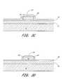
- FIG. 2illustrates a plurality of magnetic memory cells 10 with spacers 22 adjacent to the sense layers 18 .
- the spacers 22preferably comprise a nonconductive material, such as, for example, silicon nitride, diamond-like carbon, silicon carbide, or an oxide such as silicon oxide or aluminum oxide.
- the spacers 22can be formed using a variety of well-known techniques. For example, the sense layer 18 can be patterned and etched with a hard or resist mask in place, followed by the deposition of a blanket layer of nonconductive material. The resulting structure can then be subjected to a spacer etch, followed by etching through the underlying pinned layer 14 .
- the spacers 22advantageously reduce the likelihood that such a coating will form a conductive path between the sense layer 18 and the pinned layer 14 of a given memory cell 10 by largely protecting the sense layer 18 during etching of the pinned layers 14 . Therefore, the spacers 22 can advantageously reduce the number of memory cells 10 that short out, thereby increasing the yield of the manufacturing process. Even in a memory cell 10 having a spacer 22 adjacent to the sense layer 18 , however, an electrical short across the barrier layer 16 can still occur due to, inter alia, a small point of contact 24 between the coating of conductive material 20 and the sense layer 18 .
- FIGS. 3A-3Gillustrate a process for forming a magnetic memory cell 10 in accordance with one embodiment of the invention.
- the memory cell 10 of the illustrated embodimentcomprises a TMR magnetic memory cell having a particular configuration
- the memory cell 10could have a wide variety of alternative configurations.
- the pinned layer 14is the bottom layer of the memory cell 10 .
- the pinned layer 14may be the top layer of the memory cell 10 .
- the process of the illustrated embodimentbegins by depositing a pinned layer 14 , a barrier layer 16 , and a sense layer 18 on a conductive line 12 .
- the pinned layer 14may comprise a stack of magnetic and associated adjacent sublayers
- the barrier layer 16preferably comprises a nonconductive material through which electron tunneling can occur
- the sense layer 18may comprise a stack of magnetic and associated adjacent sublayers.
- both the pinned layer 14 and the sense layer 18comprise a ferromagnetic material that is an alloy of any of several metals, such as, for example, iron, nickel, and/or cobalt having a thickness preferably within the range of about 1 nm to about 30 nm, more preferably within the range of about 2.5 nm to about 20 nm, and still more preferably within the range of about 5 nm to about 10 nm.
- the barrier layer 16comprises an oxide of a metal, such as, for example, aluminum oxide, having a thickness preferably within the range of about 0.5 nm to about 3 nm, more preferably within the range of about 1 nm to about 2 ⁇ m.
- a metalsuch as, for example, aluminum oxide
- a hard mask 30can be deposited as a blanket layer over the sense layer 18 , and then patterned and etched using a variety of conventional materials and methods.
- the hard mask 30may comprise Si 3 N 4 , SiO 3 N 4 , SiC, or any other suitable hard mask material, having a thickness preferably within the range of about 100 ⁇ to about 5000 ⁇ , more preferably within the range of about 500 ⁇ to about 2000 ⁇ .
- the hard mask 30can be patterned using a number of well-known techniques, such as, for example, conventional photolithography and etching processes.
- the sense layer 18is etched in the areas that are not covered by the hard mask 30 .
- This etchcan be performed using a variety of well-known processes, such as, for example, ion milling, reactive ion etching, or chemical etching. If a process involving a chemical etchant is selected, any of a number of well-known etchants can be used, such as, for example, CO 2 —NH 3 or CO—NH 3 .
- the etching of the sense layer 18preferably stops at the barrier layer 16 .
- the hard mask 30is also partially etched during the etching of the sense layer 18 .
- the resulting structurecan be optionally oxidized to transform the outer portions of the sense layer 18 into a nonconductive material (not shown).
- This optional oxidation stepcan be performed using an oxidant such as, for example, O 3 , at a flow rate preferably within the range of about 1 sccm to about 1000 sccm, more preferably within the range of about 100 sccm to about 500 sccm.
- this optional oxidation stepinvolves using O 2 as an oxidant during a plasma oxidation process. Because this optional oxidation step reduces the amount of conductive surface area around the sides of the sense layer 18 , it advantageously reduces the likelihood of a conductive path forming between the pinned layer 14 and the sense layer 18 .
- the spacer material 22can be any suitable material (e.g., Si 3 N 4 ) but preferably comprises a low k electrical insulator, with k value preferably less than 3.5, more preferably less than 3.0.
- k valuepreferably less than 3.5, more preferably less than 3.0.
- materialsexist that can be used as the spacer material 22 , such as, for example, silicon nitride, diamond-like carbon, silicon carbide, or an oxide such as silicon oxide or aluminum oxide.
- the spacer material 22can be deposited using any suitable process, such as, for example, physical vapor deposition or chemical vapor deposition.
- the thickness of the layer of spacer material 22preferably falls within the range of about 5 nm to about 100 nm, and more preferably within the range of about 20 nm to about 40 nm.
- the layer of spacer material 22is etched, preferably using an anisotropic etch process that preferentially etches the horizontal portions of the layer of spacer material 22 relative to the vertical portions of the layer of spacer material 22 . Therefore, an etching process with a physical component is preferably used, such as an ion milling process or a reactive ion etch. In some embodiments, for example, a reactive ion etch is used with an appropriate etchant for the selected spacer material 22 .
- the spacer material 22comprises silicon nitride and the etchant comprises CF 4 or CHF 3 .
- the spacer material 22comprises diamond-like carbon and the etchant comprises oxygen-based plasma. In other exemplary embodiments, the spacer material 22 comprises silicon carbide and the etchant comprises CF 4 , CH 2 F 2 , or C 2 F 6 .
- the spacer etch processstops at the barrier layer 16 . In other embodiments, the spacer etch process continues until the pinned layer 14 is reached. In these embodiments, the barrier layer 16 is also etched as part of the same process that etches the layer of spacer material 22 .
- the remaining layersare etched.
- the process used to etch the remaining layersis substantially similar to the process used to etch the sense layer 18 .
- This processmay comprise, for example, ion milling, reactive ion etching, or chemical etching, and may use an etchant such as, for example, CO 2 —NH 3 or CO—NH 3 .
- the hard mask 30is also partially etched during the etching of the pinned layer 14 .
- a thin coating of conductive material 20may form along the sidewalls of the memory cell 10 .
- the thin coating of conductive material 20may comprise particles of the pinned layer 14 that are thrown up as byproducts of the etching process of the pinned layer 14 .
- the thin coating of conductive material 20may form a conductive path between the pinned layer 14 and the sense layer 18 , thereby creating an electrical short across the barrier layer 16 that can cause the memory cell 10 to malfunction.
- the spacers 22minimize the amount of exposed conductive surface area around the sides of the sense layer 18 , and thus reduce the likelihood of a conductive path forming between the pinned layer 14 and the sense layer 18 , such a conductive path can still exist if there is even only a small point of contact 24 between the thin coating of conductive material 20 and the sense layer 18 .
- the thin coating of conductive material 20can be oxidized to transform the conductive material 20 into a nonconductive material 36 , as illustrated in FIG. 3F .
- This oxidation stepcan be performed using an oxidant such as, for example, O 3 , at a flow rate preferably within the range of about 1 sccm to about 1000 sccm, more preferably within the range of about 100 sccm to about 500 sccm.
- this oxidation stepinvolves using O 2 as an oxidant during a plasma oxidation process.
- the thin coating of nonconductive material 36is illustrated as one continuous layer in FIGS. 3E-3F , it may be formed as a discontinuous layer.
- the remaining portion of the hard mask 30is removed to complete the process of forming the memory cell 10 .
- the conductive material 20By oxidizing the conductive material 20 , thereby transforming it into a nonconductive material 36 , the likelihood of a conductive path forming between the pinned layer 14 and the sense layer 18 due to a small point of contact 24 between the layer of nonconductive material 36 and the sense layer 18 is substantially reduced. Accordingly, the number of memory cells 10 within an MRAM array that malfunction due to electrical shorts is reduced, and the yield of the manufacturing process for the MRAM device is advantageously improved.
- FIGS. 4A-4Gillustrate an alternative process for forming a magnetic memory cell 10 in accordance with one embodiment of the invention, which is somewhat similar to the embodiment of the invention described above.
- the processbegins with the same steps described above in connection with FIGS. 3A-3B .
- the resulting structureis repeatedly subjected to alternating partial oxidation and partial etch steps until the memory cell 10 is formed.
- the partial oxidation stepsare performed by subjecting the structure to plasma oxidation using a process that is substantially similar to the optional oxidation step described above in connection with FIG. 3B .
- FIG. 4Cwhen the structure is subjected to plasma oxidation, the outer or sidewall portions 40 of the sense layer 18 and the upper portion 42 of the pinned layer 14 are transformed into a nonconductive material, except for the portions that are protected under the hard mask 30 .
- the pinned layer 14can then be partially etched because, even if particles from the upper portion of the pinned layer 14 are deposited along the sidewalls of the structure as byproducts of the etching process, the particles are nonconductive and thus unlikely to cause an electrical short across the barrier layer 16 .
- the grown sidewall spacer in the form of outer portions 40further reduces the likelihood of a short forming across the barrier layer 16 .
- an etching process with a physical componentis preferably used, such as an ion milling process or a reactive ion etch. The partial etch preferably stops before the portion of the pinned layer 14 below the upper portion 42 is reached, such that only nonconductive particles tend to be thrown up along the sidewalls of the memory cell 10 as byproducts of the etching process.
- the steps illustrated in FIGS. 4C-4Dcan be repeated cyclically until the entire pinned layer 14 has been oxidized and etched. In a preferred embodiment, both the oxidation and the etching steps can be performed in situ within the same tool. Then, as illustrated in FIG. 4E , the remaining portion of the hard mask 30 can be removed to complete the process of forming the memory cell 10 .
- the likelihood of a conductive path forming between the pinned layer 14 and the sense layer 18is substantially reduced. Accordingly, the number of memory cells 10 within an MRAM array that malfunction due to electrical shorts is reduced, and the yield of the manufacturing process for the MRAM device is advantageously improved.
- the process illustrated in FIGS. 4A-4Eis advantageously self-aligning because the region under the hard mask 30 is protected from both oxidation and etching. Therefore, although the process involves repeating a series of alternating oxidation and etching steps, the process involves only a single masking step. Because no additional masks are needed to perform the alternating oxidation and etching steps, the process can advantageously be performed at a relatively low cost.
Landscapes
- Engineering & Computer Science (AREA)
- Manufacturing & Machinery (AREA)
- Mram Or Spin Memory Techniques (AREA)
- Hall/Mr Elements (AREA)
Abstract
Description
- 1. Field of the Invention
- The present invention relates to magnetic random access memory (MRAM) devices. More specifically, the present invention relates to reducing electrical shorting in the memory cells of an MRAM device.
- 2. Description of the Related Art
- Magnetic random access memory (MRAM) is a well-known form of memory. In an MRAM device, digital bits of information can be stored as alternative directions of magnetization in a magnetic storage element or cell. The storage elements may be simple structures, such as thin ferromagnetic films, or more complex layered magnetic thin-film structures, such as tunneling magnetoresistance (TMR) or giant magnetoresistance (GMR) elements.
- An exemplary TMR memory cell comprises two magnetic layers separated by a barrier layer. One magnetic layer, referred to as the “pinned” layer, has a fixed magnetization direction, whereas the magnetization direction of the other magnetic layer, referred to as the “sense” layer, can be reversed by applying a magnetic field that is not strong enough to affect the magnetization direction of the pinned layer.
- A TMR memory cell can operate by allowing a quantum mechanical tunneling of electrons from one magnetic layer to the other through the barrier layer of the cell. The passage of electrons through the barrier layer depends upon the magnetization direction of the sense layer relative to that of the pinned layer. Electrons pass more freely when the magnetic directions of the layers are aligned and less freely when the magnetic directions of the layers are not aligned. Therefore, the state of a memory cell can be determined by observing the degree of electron tunneling through the barrier layer. GMR memory cells operate similarly by sensing current flow or resistance through aligned or anti-aligned magnetic layers, rather than by employing a tunneling dielectric.
- A TMR memory cell cannot function properly unless the sense layer and the pinned layer of the cell are electrically isolated from one another. If a short circuit occurs between these two layers, then there will be no tunneling of electrons through the barrier layer.
- A plurality of magnetic memory cells can be organized into an array having any of a wide variety of configurations. One exemplary configuration is a “cross-point” memory array, which comprises a first set of parallel conductive lines covered by an insulating layer, over which lies a second set of parallel conductive lines, perpendicular to the first lines. One set of conductive lines is referred to as the “bit” lines, and the other set of conductive lines is referred to as the “word” lines. The magnetic memory cells can be sandwiched between the bit lines and the word lines at their intersections.
- In one embodiment of the present invention, a method of forming a magnetic memory cell comprises providing a first conductive layer as a blanket layer, providing a barrier layer as a blanket layer over the first conductive layer, and providing a second conductive layer as a blanket layer over the barrier layer. The method further comprises providing a hard mask over the second conductive layer, wherein the hard mask defines the region in which the magnetic memory cell is formed, etching the second conductive layer to form an upper portion of the magnetic memory cell, and forming a spacer around the upper portion of the magnetic memory cell. The method further comprises etching the barrier layer and the first conductive layer to form a lower portion of the magnetic memory cell, wherein conductive particles of the first conductive layer may be thrown up along a sidewall of the magnetic memory cell as byproducts of the etching of the first conductive layer, and oxidizing the magnetic memory cell, thereby transforming the conductive particles into nonconductive particles.
- In another embodiment, a method of forming a magnetic memory cell comprises providing a first conductive layer, a barrier layer, and a second conductive layer as blanket layers, providing a hard mask over the second conductive layer, wherein the hard mask defines the region in which the magnetic memory cell is formed, and etching the second conductive layer and the barrier layer to form an upper portion of the magnetic memory cell. The method further comprises partially oxidizing the first conductive layer such that at least a portion of the first conductive layer is transformed into an insulating material, at least partially etching the portion of the first conductive layer that was transformed into an insulating material during the partial oxidizing step, and repeating the partial oxidizing and partial etching steps until the first conductive layer forms a lower portion of the magnetic memory cell.
- In another embodiment, a magnetic memory cell comprises a lower layer comprising a first conductive material, a middle layer comprising an insulating material, and an upper layer comprising a second conductive material. The magnetic memory cell further comprises a nonconductive layer comprising an oxide of the first conductive material, wherein the nonconductive layer is coated along a sidewall of the magnetic memory cell such that it can be in contact with both the upper and lower layers.
- In another embodiment, a magnetic memory cell comprises a lower layer comprising a first conductive material and a middle layer comprising an insulating material. The magnetic memory cell further comprises an upper layer comprising a second conductive material surrounded by a spacer material and at least one sidewall coated with oxidized particles of the first conductive material.
- These and other features and advantages of the invention will now be described with reference to the drawings of certain preferred embodiments, which are intended to illustrate, and not to limit, the invention. In the figures, like reference numerals are used to refer to like elements.
FIG. 1 illustrates a plurality of conventional TMR magnetic memory cells.FIG. 2 illustrates a plurality of magnetic memory cells with insulating spacers adjacent to the sense layers.FIGS. 3A-3G illustrate the formation of a magnetic memory cell in accordance with one embodiment of the invention.FIGS. 4A-4E illustrate the formation of a magnetic memory cell in accordance with another embodiment of the invention.- For purposes of illustration, various embodiments of the invention will be described in the context of a TMR magnetic memory cell having a particular configuration. The details associated with this specific configuration are set forth to illustrate, and not to limit, the invention. For example, the invention can be implemented with TMR magnetic memory cells having alternative configurations or with other types of memory cells. The scope of the invention is defined only by the appended claims.
FIG. 1 illustrates a plurality of conventionalmagnetic memory cells 10 formed on a metal conductingline 12, preferably copper or aluminum, which is deposited on a substrate (not shown). The conductingline 12 extends to the right and to the left of the page. Thememory cells 10 can be formed by first depositing a pinnedlayer 14 on the conductingline 12, depositing aninsulating barrier layer 16 over the pinnedlayer 14, and depositing asense layer 18 over thebarrier layer 16. The pinnedlayer 14,barrier layer 16, andsense layer 18 can then be patterned and etched to form thememory cells 10 using methods that are well-known to those of skill in the art.- The pinned
layer 14 may comprise a stack of magnetic and associated adjacent sublayers. For example, the pinnedlayer 14 may comprise a tantalum seed sublayer, a nickel-iron seed sublayer, a magnesium oxide, irridium-manganese, platinum-manganese or nickel-manganese pinning sublayer, and a nickel-iron, nickel-iron-cobalt, cobalt-iron or nickel-iron-chromium sublayer. Thebarrier layer 16 is preferably thin enough to allow the tunneling of electrons from thesense layer 18 to thepinned layer 14. Thebarrier layer 16 may comprise, for example, aluminum oxide, having a thickness within the range of about 0.5 nm to about 3 nm, preferably within the range of about 1 nm to about 2 nm. Like thepinned layer 14, thesense layer 18 may comprise a stack of magnetic and associated adjacent blanket sublayers. For example, thesense layer 18 may comprise a tantalum sublayer, a tungsten nitride sublayer, and a nickel-iron, nickel-iron-cobalt, cobalt-iron, cobalt or copper sublayer. - During the fabrication of a conventional
magnetic memory cell 10, it is common for a thin coating ofconductive material 20 to form along the sidewalls of thememory cell 10, as illustrated inFIG. 1 . This coating ofconductive material 20 may comprise, for example, particles of thepinned layer 14 that are thrown up along the sidewalls of thememory cell 10 during the process of etching through the pinnedlayer 14, particularly if an etching process with a physical component is used, such as an ion milling process or a reactive ion etch. - The thin coating of
conductive material 20 along the sidewalls of thememory cell 10 is undesirable because it can create a conductive path between the pinnedlayer 14 and thesense layer 18. Such a conductive path creates an electrical short across thebarrier layer 16 that can prevent thememory cell 10 from functioning properly. Therefore, the coating ofconductive material 20 along the sidewalls of thememory cells 10 can undesirably reduce the yield of the manufacturing process. Although an additional cleaning step can be performed to remove the coating ofconductive material 20 from the sidewalls of thememory cells 10, such an additional step can add cost to the manufacturing process and can also have a harmful effect on the remaining structures. FIG. 2 illustrates a plurality ofmagnetic memory cells 10 withspacers 22 adjacent to thesense layers 18. Thespacers 22 preferably comprise a nonconductive material, such as, for example, silicon nitride, diamond-like carbon, silicon carbide, or an oxide such as silicon oxide or aluminum oxide. Thespacers 22 can be formed using a variety of well-known techniques. For example, thesense layer 18 can be patterned and etched with a hard or resist mask in place, followed by the deposition of a blanket layer of nonconductive material. The resulting structure can then be subjected to a spacer etch, followed by etching through the underlying pinnedlayer 14.- Although a coating of
conductive material 20 can form along the sidewalls of thememory cells 10, thespacers 22 advantageously reduce the likelihood that such a coating will form a conductive path between thesense layer 18 and the pinnedlayer 14 of a givenmemory cell 10 by largely protecting thesense layer 18 during etching of the pinned layers14. Therefore, thespacers 22 can advantageously reduce the number ofmemory cells 10 that short out, thereby increasing the yield of the manufacturing process. Even in amemory cell 10 having aspacer 22 adjacent to thesense layer 18, however, an electrical short across thebarrier layer 16 can still occur due to, inter alia, a small point ofcontact 24 between the coating ofconductive material 20 and thesense layer 18. FIGS. 3A-3G illustrate a process for forming amagnetic memory cell 10 in accordance with one embodiment of the invention. Although thememory cell 10 of the illustrated embodiment comprises a TMR magnetic memory cell having a particular configuration, thememory cell 10 could have a wide variety of alternative configurations. For example, in the illustrated embodiment, the pinnedlayer 14 is the bottom layer of thememory cell 10. In other embodiments, the pinnedlayer 14 may be the top layer of thememory cell 10. These and many other variations will become apparent to those of skill in the art in view of the present disclosure.- The process of the illustrated embodiment begins by depositing a pinned
layer 14, abarrier layer 16, and asense layer 18 on aconductive line 12. As discussed above, the pinnedlayer 14 may comprise a stack of magnetic and associated adjacent sublayers, thebarrier layer 16 preferably comprises a nonconductive material through which electron tunneling can occur, and thesense layer 18 may comprise a stack of magnetic and associated adjacent sublayers. - These layers can be formed using a wide variety of well-known methods and materials. For example, in some embodiments, both the pinned
layer 14 and thesense layer 18 comprise a ferromagnetic material that is an alloy of any of several metals, such as, for example, iron, nickel, and/or cobalt having a thickness preferably within the range of about 1 nm to about 30 nm, more preferably within the range of about 2.5 nm to about 20 nm, and still more preferably within the range of about 5 nm to about 10 nm. In some embodiments, thebarrier layer 16 comprises an oxide of a metal, such as, for example, aluminum oxide, having a thickness preferably within the range of about 0.5 nm to about 3 nm, more preferably within the range of about 1 nm to about 2 μm. Those of ordinary skill in the art will understand that these materials and thickness ranges are exemplary, and that different materials having different thicknesses could be used. - As illustrated in
FIG. 3A , ahard mask 30 can be deposited as a blanket layer over thesense layer 18, and then patterned and etched using a variety of conventional materials and methods. For example, thehard mask 30 may comprise Si3N4, SiO3N4, SiC, or any other suitable hard mask material, having a thickness preferably within the range of about 100 Å to about 5000 Å, more preferably within the range of about 500 Å to about 2000 Å. Thehard mask 30 can be patterned using a number of well-known techniques, such as, for example, conventional photolithography and etching processes. - As illustrated in
FIG. 3B , thesense layer 18 is etched in the areas that are not covered by thehard mask 30. This etch can be performed using a variety of well-known processes, such as, for example, ion milling, reactive ion etching, or chemical etching. If a process involving a chemical etchant is selected, any of a number of well-known etchants can be used, such as, for example, CO2—NH3or CO—NH3. The etching of thesense layer 18 preferably stops at thebarrier layer 16. Thehard mask 30 is also partially etched during the etching of thesense layer 18. - After the
sense layer 18 is etched, the resulting structure can be optionally oxidized to transform the outer portions of thesense layer 18 into a nonconductive material (not shown). This optional oxidation step can be performed using an oxidant such as, for example, O3, at a flow rate preferably within the range of about 1 sccm to about 1000 sccm, more preferably within the range of about 100 sccm to about 500 sccm. In other embodiments, this optional oxidation step involves using O2as an oxidant during a plasma oxidation process. Because this optional oxidation step reduces the amount of conductive surface area around the sides of thesense layer 18, it advantageously reduces the likelihood of a conductive path forming between the pinnedlayer 14 and thesense layer 18. - As illustrated in
FIG. 3C , a blanket layer ofspacer material 22 is deposited over the existing layers. Thespacer material 22 can be any suitable material (e.g., Si3N4) but preferably comprises a low k electrical insulator, with k value preferably less than 3.5, more preferably less than 3.0. A variety of materials exist that can be used as thespacer material 22, such as, for example, silicon nitride, diamond-like carbon, silicon carbide, or an oxide such as silicon oxide or aluminum oxide. - The
spacer material 22 can be deposited using any suitable process, such as, for example, physical vapor deposition or chemical vapor deposition. In some embodiments, the thickness of the layer ofspacer material 22 preferably falls within the range of about 5 nm to about 100 nm, and more preferably within the range of about 20 nm to about 40 nm. - As illustrated in
FIG. 3D , the layer ofspacer material 22 is etched, preferably using an anisotropic etch process that preferentially etches the horizontal portions of the layer ofspacer material 22 relative to the vertical portions of the layer ofspacer material 22. Therefore, an etching process with a physical component is preferably used, such as an ion milling process or a reactive ion etch. In some embodiments, for example, a reactive ion etch is used with an appropriate etchant for the selectedspacer material 22. For example, in some embodiments, thespacer material 22 comprises silicon nitride and the etchant comprises CF4or CHF3. In other exemplary embodiments, thespacer material 22 comprises diamond-like carbon and the etchant comprises oxygen-based plasma. In other exemplary embodiments, thespacer material 22 comprises silicon carbide and the etchant comprises CF4, CH2F2, or C2F6. - In the embodiment illustrated in
FIG. 3D , the spacer etch process stops at thebarrier layer 16. In other embodiments, the spacer etch process continues until the pinnedlayer 14 is reached. In these embodiments, thebarrier layer 16 is also etched as part of the same process that etches the layer ofspacer material 22. - As illustrated in
FIG. 3E , after the spacer etch process is complete, the remaining layers are etched. In some embodiments, the process used to etch the remaining layers is substantially similar to the process used to etch thesense layer 18. This process may comprise, for example, ion milling, reactive ion etching, or chemical etching, and may use an etchant such as, for example, CO2—NH3or CO—NH3. Thehard mask 30 is also partially etched during the etching of the pinnedlayer 14. - As the pinned
layer 14 is etched, a thin coating ofconductive material 20 may form along the sidewalls of thememory cell 10. The thin coating ofconductive material 20 may comprise particles of the pinnedlayer 14 that are thrown up as byproducts of the etching process of the pinnedlayer 14. As discussed above, the thin coating ofconductive material 20 may form a conductive path between the pinnedlayer 14 and thesense layer 18, thereby creating an electrical short across thebarrier layer 16 that can cause thememory cell 10 to malfunction. Although thespacers 22 minimize the amount of exposed conductive surface area around the sides of thesense layer 18, and thus reduce the likelihood of a conductive path forming between the pinnedlayer 14 and thesense layer 18, such a conductive path can still exist if there is even only a small point ofcontact 24 between the thin coating ofconductive material 20 and thesense layer 18. - Accordingly, to further reduce the likelihood of a conductive path forming between the pinned
layer 14 and thesense layer 18, the thin coating ofconductive material 20 can be oxidized to transform theconductive material 20 into anonconductive material 36, as illustrated inFIG. 3F . This oxidation step can be performed using an oxidant such as, for example, O3, at a flow rate preferably within the range of about 1 sccm to about 1000 sccm, more preferably within the range of about 100 sccm to about 500 sccm. In other embodiments, this oxidation step involves using O2as an oxidant during a plasma oxidation process. It should be understood that, although the thin coating ofnonconductive material 36 is illustrated as one continuous layer inFIGS. 3E-3F , it may be formed as a discontinuous layer. - As illustrated in
FIG. 3G , the remaining portion of thehard mask 30 is removed to complete the process of forming thememory cell 10. By oxidizing theconductive material 20, thereby transforming it into anonconductive material 36, the likelihood of a conductive path forming between the pinnedlayer 14 and thesense layer 18 due to a small point ofcontact 24 between the layer ofnonconductive material 36 and thesense layer 18 is substantially reduced. Accordingly, the number ofmemory cells 10 within an MRAM array that malfunction due to electrical shorts is reduced, and the yield of the manufacturing process for the MRAM device is advantageously improved. FIGS. 4A-4G illustrate an alternative process for forming amagnetic memory cell 10 in accordance with one embodiment of the invention, which is somewhat similar to the embodiment of the invention described above. For example, as illustrated inFIGS. 4A-4B , the process begins with the same steps described above in connection withFIGS. 3A-3B .- In the present embodiment, however, after the
sense layer 18 is etched, the resulting structure is repeatedly subjected to alternating partial oxidation and partial etch steps until thememory cell 10 is formed. In some embodiments, the partial oxidation steps are performed by subjecting the structure to plasma oxidation using a process that is substantially similar to the optional oxidation step described above in connection withFIG. 3B . As illustrated inFIG. 4C , when the structure is subjected to plasma oxidation, the outer orsidewall portions 40 of thesense layer 18 and theupper portion 42 of the pinnedlayer 14 are transformed into a nonconductive material, except for the portions that are protected under thehard mask 30. - As illustrated in
FIG. 4D , the pinnedlayer 14 can then be partially etched because, even if particles from the upper portion of the pinnedlayer 14 are deposited along the sidewalls of the structure as byproducts of the etching process, the particles are nonconductive and thus unlikely to cause an electrical short across thebarrier layer 16. In addition, the grown sidewall spacer in the form ofouter portions 40 further reduces the likelihood of a short forming across thebarrier layer 16. To perform the partial etch of the pinnedlayer 14, an etching process with a physical component is preferably used, such as an ion milling process or a reactive ion etch. The partial etch preferably stops before the portion of the pinnedlayer 14 below theupper portion 42 is reached, such that only nonconductive particles tend to be thrown up along the sidewalls of thememory cell 10 as byproducts of the etching process. - The steps illustrated in
FIGS. 4C-4D can be repeated cyclically until the entire pinnedlayer 14 has been oxidized and etched. In a preferred embodiment, both the oxidation and the etching steps can be performed in situ within the same tool. Then, as illustrated inFIG. 4E , the remaining portion of thehard mask 30 can be removed to complete the process of forming thememory cell 10. By repeatedly partially oxidizing and etching the pinnedlayer 14 such that only nonconductive particles can be deposited along the sidewalls of thememory cell 10 during the fabrication process, the likelihood of a conductive path forming between the pinnedlayer 14 and thesense layer 18 is substantially reduced. Accordingly, the number ofmemory cells 10 within an MRAM array that malfunction due to electrical shorts is reduced, and the yield of the manufacturing process for the MRAM device is advantageously improved. - In addition, the process illustrated in
FIGS. 4A-4E is advantageously self-aligning because the region under thehard mask 30 is protected from both oxidation and etching. Therefore, although the process involves repeating a series of alternating oxidation and etching steps, the process involves only a single masking step. Because no additional masks are needed to perform the alternating oxidation and etching steps, the process can advantageously be performed at a relatively low cost. - Although this invention has been described in terms of certain preferred embodiments, other embodiments that are apparent to those of ordinary skill in the art, including embodiments that do not provide all of the features and advantages set forth herein, are also within the scope of this invention. Accordingly, the scope of the present invention is defined only by reference to the appended claims.
Claims (57)
Priority Applications (3)
| Application Number | Priority Date | Filing Date | Title |
|---|---|---|---|
| US10/684,967US7112454B2 (en) | 2003-10-14 | 2003-10-14 | System and method for reducing shorting in memory cells |
| US11/412,582US7358553B2 (en) | 2003-10-14 | 2006-04-27 | System and method for reducing shorting in memory cells |
| US11/535,456US7855085B2 (en) | 2003-10-14 | 2006-09-26 | System and method for reducing shorting in memory cells |
Applications Claiming Priority (1)
| Application Number | Priority Date | Filing Date | Title |
|---|---|---|---|
| US10/684,967US7112454B2 (en) | 2003-10-14 | 2003-10-14 | System and method for reducing shorting in memory cells |
Related Child Applications (2)
| Application Number | Title | Priority Date | Filing Date |
|---|---|---|---|
| US11/412,582DivisionUS7358553B2 (en) | 2003-10-14 | 2006-04-27 | System and method for reducing shorting in memory cells |
| US11/535,456ContinuationUS7855085B2 (en) | 2003-10-14 | 2006-09-26 | System and method for reducing shorting in memory cells |
Publications (2)
| Publication Number | Publication Date |
|---|---|
| US20050079638A1true US20050079638A1 (en) | 2005-04-14 |
| US7112454B2 US7112454B2 (en) | 2006-09-26 |
Family
ID=34423062
Family Applications (3)
| Application Number | Title | Priority Date | Filing Date |
|---|---|---|---|
| US10/684,967Expired - LifetimeUS7112454B2 (en) | 2003-10-14 | 2003-10-14 | System and method for reducing shorting in memory cells |
| US11/412,582Expired - LifetimeUS7358553B2 (en) | 2003-10-14 | 2006-04-27 | System and method for reducing shorting in memory cells |
| US11/535,456Active2026-04-08US7855085B2 (en) | 2003-10-14 | 2006-09-26 | System and method for reducing shorting in memory cells |
Family Applications After (2)
| Application Number | Title | Priority Date | Filing Date |
|---|---|---|---|
| US11/412,582Expired - LifetimeUS7358553B2 (en) | 2003-10-14 | 2006-04-27 | System and method for reducing shorting in memory cells |
| US11/535,456Active2026-04-08US7855085B2 (en) | 2003-10-14 | 2006-09-26 | System and method for reducing shorting in memory cells |
Country Status (1)
| Country | Link |
|---|---|
| US (3) | US7112454B2 (en) |
Cited By (12)
| Publication number | Priority date | Publication date | Assignee | Title |
|---|---|---|---|---|
| US20050030786A1 (en)* | 2002-05-02 | 2005-02-10 | Micron Technology, Inc. | Low remanence flux concentrator for MRAM devices |
| US7002228B2 (en) | 2003-02-18 | 2006-02-21 | Micron Technology, Inc. | Diffusion barrier for improving the thermal stability of MRAM devices |
| US20070166840A1 (en)* | 2006-01-18 | 2007-07-19 | International Business Machines Corporation | Utilizing sidewall spacer features to form magnetic tunnel junctions in an integrated circuit |
| WO2010056721A1 (en) | 2008-11-11 | 2010-05-20 | Seagate Technology | Magnetic memory cells with radial barrier |
| US20100178714A1 (en)* | 2009-01-09 | 2010-07-15 | Samsung Electronics Co., Ltd. | Method of forming magnetic memory device |
| CN102479918A (en)* | 2010-11-29 | 2012-05-30 | 三星电子株式会社 | Method for forming magnetic tunnel junction structure and method for forming magnetic random access memory |
| WO2014164520A1 (en) | 2013-03-11 | 2014-10-09 | Dafna Beery | Magnetic random access memory cells with isolating liners |
| US20150340601A1 (en)* | 2014-05-21 | 2015-11-26 | Avalanche Technology, Inc. | Magnetic random access memory with multilayered seed structure |
| US10050083B2 (en) | 2014-05-21 | 2018-08-14 | Avalanche Technology, Inc. | Magnetic structure with multilayered seed |
| US10347691B2 (en) | 2014-05-21 | 2019-07-09 | Avalanche Technology, Inc. | Magnetic memory element with multilayered seed structure |
| US10438997B2 (en) | 2014-05-21 | 2019-10-08 | Avalanche Technology, Inc. | Multilayered seed structure for magnetic memory element including a CoFeB seed layer |
| EP3673522B1 (en)* | 2017-08-23 | 2022-10-05 | Everspin Technologies, Inc. | Magnetoresistive bit fabrication by multi-step etching |
Families Citing this family (15)
| Publication number | Priority date | Publication date | Assignee | Title |
|---|---|---|---|---|
| US7112454B2 (en)* | 2003-10-14 | 2006-09-26 | Micron Technology, Inc. | System and method for reducing shorting in memory cells |
| US7115525B2 (en)* | 2004-09-02 | 2006-10-03 | Micron Technology, Inc. | Method for integrated circuit fabrication using pitch multiplication |
| US8123968B2 (en) | 2005-08-25 | 2012-02-28 | Round Rock Research, Llc | Multiple deposition for integration of spacers in pitch multiplication process |
| US7923373B2 (en) | 2007-06-04 | 2011-04-12 | Micron Technology, Inc. | Pitch multiplication using self-assembling materials |
| KR101870873B1 (en)* | 2011-08-04 | 2018-07-20 | 에스케이하이닉스 주식회사 | Method for fabricating magnetic tunnel junction device |
| US8615868B2 (en) | 2011-11-29 | 2013-12-31 | HGST Netherlands B.V. | Method for manufacturing a magnetic sensor using two step ion milling |
| US8976569B2 (en) | 2013-01-30 | 2015-03-10 | Hewlett-Packard Development Company, L.P. | Mitigation of inoperable low resistance elements in programable crossbar arrays |
| CN105814679A (en) | 2013-06-28 | 2016-07-27 | 英特尔公司 | Preservation of fine pitch redistribution lines |
| KR102082322B1 (en) | 2013-08-09 | 2020-02-27 | 삼성전자주식회사 | Method of forming magnetic memory devices |
| EP3123476B1 (en) | 2014-03-28 | 2019-10-16 | Intel Corporation | Techniques for forming spin-transfer-torque memory having a dot-contacted free magnetic layer |
| US9349939B2 (en)* | 2014-05-23 | 2016-05-24 | Qualcomm Incorporated | Etch-resistant protective coating for a magnetic tunnel junction device |
| CN109560102A (en)* | 2017-09-26 | 2019-04-02 | 中电海康集团有限公司 | MRAM and its production method |
| CN109378386B (en)* | 2018-10-16 | 2022-06-07 | 南京邮电大学 | Method for regulating the morphology of lead-free perovskite solar cells and prepared battery devices |
| US11302630B2 (en)* | 2020-04-08 | 2022-04-12 | International Business Machines Corporation | Electrode-via structure |
| US11849644B2 (en)* | 2021-04-15 | 2023-12-19 | Taiwan Semiconductor Manufacturing Company, Ltd. | Method of fabricating magneto-resistive random access memory (MRAM) |
Citations (49)
| Publication number | Priority date | Publication date | Assignee | Title |
|---|---|---|---|---|
| US3623035A (en)* | 1968-02-02 | 1971-11-23 | Fuji Electric Co Ltd | Magnetic memory matrix and process for its production |
| US3623032A (en)* | 1970-02-16 | 1971-11-23 | Honeywell Inc | Keeper configuration for a thin-film memory |
| US3816909A (en)* | 1969-04-30 | 1974-06-18 | Hitachi Chemical Co Ltd | Method of making a wire memory plane |
| US3947831A (en)* | 1972-12-11 | 1976-03-30 | Kokusai Denshin Denwa Kabushiki Kaisha | Word arrangement matrix memory of high bit density having a magnetic flux keeper |
| US4044330A (en)* | 1976-03-30 | 1977-08-23 | Honeywell Information Systems, Inc. | Power strobing to achieve a tri state |
| US4060794A (en)* | 1976-03-31 | 1977-11-29 | Honeywell Information Systems Inc. | Apparatus and method for generating timing signals for latched type memories |
| US4158891A (en)* | 1975-08-18 | 1979-06-19 | Honeywell Information Systems Inc. | Transparent tri state latch |
| US4455626A (en)* | 1983-03-21 | 1984-06-19 | Honeywell Inc. | Thin film memory with magnetoresistive read-out |
| US4731757A (en)* | 1986-06-27 | 1988-03-15 | Honeywell Inc. | Magnetoresistive memory including thin film storage cells having tapered ends |
| US4780848A (en)* | 1986-06-03 | 1988-10-25 | Honeywell Inc. | Magnetoresistive memory with multi-layer storage cells having layers of limited thickness |
| US4801883A (en)* | 1986-06-02 | 1989-01-31 | The Regents Of The University Of California | Integrated-circuit one-way isolation coupler incorporating one or several carrier-domain magnetometers |
| US4945397A (en)* | 1986-12-08 | 1990-07-31 | Honeywell Inc. | Resistive overlayer for magnetic films |
| US5039655A (en)* | 1989-07-28 | 1991-08-13 | Ampex Corporation | Thin film memory device having superconductor keeper for eliminating magnetic domain creep |
| US5064499A (en)* | 1990-04-09 | 1991-11-12 | Honeywell Inc. | Inductively sensed magnetic memory manufacturing method |
| US5140549A (en)* | 1990-04-09 | 1992-08-18 | Honeywell Inc. | Inductively sensed magnetic memory |
| US5496759A (en)* | 1994-12-29 | 1996-03-05 | Honeywell Inc. | Highly producible magnetoresistive RAM process |
| US5547599A (en)* | 1989-03-17 | 1996-08-20 | Raytheon Company | Ferrite/epoxy film |
| US5569619A (en)* | 1992-06-24 | 1996-10-29 | Lg Semicon Co., Ltd. | Method for forming a capacitor of a semiconductor memory cell |
| US5587943A (en)* | 1995-02-13 | 1996-12-24 | Integrated Microtransducer Electronics Corporation | Nonvolatile magnetoresistive memory with fully closed flux operation |
| US5650958A (en)* | 1996-03-18 | 1997-07-22 | International Business Machines Corporation | Magnetic tunnel junctions with controlled magnetic response |
| US5701222A (en)* | 1995-09-11 | 1997-12-23 | International Business Machines Corporation | Spin valve sensor with antiparallel magnetization of pinned layers |
| US5726498A (en)* | 1995-05-26 | 1998-03-10 | International Business Machines Corporation | Wire shape conferring reduced crosstalk and formation methods |
| US5741435A (en)* | 1995-08-08 | 1998-04-21 | Nano Systems, Inc. | Magnetic memory having shape anisotropic magnetic elements |
| US5756366A (en)* | 1995-12-21 | 1998-05-26 | Honeywell Inc. | Magnetic hardening of bit edges of magnetoresistive RAM |
| US5804458A (en)* | 1996-12-16 | 1998-09-08 | Motorola, Inc. | Method of fabricating spaced apart submicron magnetic memory cells |
| US5861328A (en)* | 1996-10-07 | 1999-01-19 | Motorola, Inc. | Method of fabricating GMR devices |
| US5926394A (en)* | 1996-09-30 | 1999-07-20 | Intel Corporation | Method and apparatus for regulating the voltage supplied to an integrated circuit |
| US5956267A (en)* | 1997-12-18 | 1999-09-21 | Honeywell Inc | Self-aligned wordline keeper and method of manufacture therefor |
| US5982658A (en)* | 1997-10-31 | 1999-11-09 | Honeywell Inc. | MRAM design to reduce dissimilar nearest neighbor effects |
| US6028786A (en)* | 1997-04-28 | 2000-02-22 | Canon Kabushiki Kaisha | Magnetic memory element having coupled magnetic layers forming closed magnetic circuit |
| US6048739A (en)* | 1997-12-18 | 2000-04-11 | Honeywell Inc. | Method of manufacturing a high density magnetic memory device |
| US6136705A (en)* | 1998-10-22 | 2000-10-24 | National Semiconductor Corporation | Self-aligned dual thickness cobalt silicide layer formation process |
| US6153443A (en)* | 1998-12-21 | 2000-11-28 | Motorola, Inc. | Method of fabricating a magnetic random access memory |
| US6174737B1 (en)* | 1998-08-31 | 2001-01-16 | Motorola, Inc. | Magnetic random access memory and fabricating method thereof |
| US6218302B1 (en)* | 1998-07-21 | 2001-04-17 | Motorola Inc. | Method for forming a semiconductor device |
| US6338899B1 (en)* | 1998-06-30 | 2002-01-15 | Kabushiki Kaisha Toshiba | Magnetoresistance effect element, magnetic head, magnetic head assembly, magnetic storage system |
| US6358756B1 (en)* | 2001-02-07 | 2002-03-19 | Micron Technology, Inc. | Self-aligned, magnetoresistive random-access memory (MRAM) structure utilizing a spacer containment scheme |
| US20020041514A1 (en)* | 1999-02-26 | 2002-04-11 | Ulrich Scheler | Memory cell configuration and method for its production |
| US6379978B2 (en)* | 1998-07-15 | 2002-04-30 | Infineon Technologies Ag | Memory cell configuration in which an electrical resistance of a memory element represents an information item and can be influenced by a magnetic field, and method for fabricating it |
| US6392922B1 (en)* | 2000-08-14 | 2002-05-21 | Micron Technology, Inc. | Passivated magneto-resistive bit structure and passivation method therefor |
| US6391658B1 (en)* | 1999-10-26 | 2002-05-21 | International Business Machines Corporation | Formation of arrays of microelectronic elements |
| US20020076572A1 (en)* | 2000-09-29 | 2002-06-20 | Manfred Engelhardt | Method for fabricating integrated circuit arrangements, and associated circuit arrangements, in particular tunnel contact elements |
| US6440753B1 (en)* | 2001-01-24 | 2002-08-27 | Infineon Technologies North America Corp. | Metal hard mask for ILD RIE processing of semiconductor memory devices to prevent oxidation of conductive lines |
| US6485989B1 (en)* | 2001-08-30 | 2002-11-26 | Micron Technology, Inc. | MRAM sense layer isolation |
| US6627913B2 (en)* | 2001-09-10 | 2003-09-30 | Micron Technology, Inc. | Insulation of an MRAM device through a self-aligned spacer |
| US6770491B2 (en)* | 2002-08-07 | 2004-08-03 | Micron Technology, Inc. | Magnetoresistive memory and method of manufacturing the same |
| US6783995B2 (en)* | 2002-04-30 | 2004-08-31 | Micron Technology, Inc. | Protective layers for MRAM devices |
| US6855563B2 (en)* | 2002-05-01 | 2005-02-15 | Sony Corporation | Method of manufacturing a tunnel magneto-resistance based magnetic memory device |
| US6911156B2 (en)* | 2003-04-16 | 2005-06-28 | Freescale Semiconductor, Inc. | Methods for fabricating MRAM device structures |
Family Cites Families (19)
| Publication number | Priority date | Publication date | Assignee | Title |
|---|---|---|---|---|
| JP3350955B2 (en)* | 1992-05-18 | 2002-11-25 | 株式会社日立製作所 | Method for repairing semiconductor device |
| US6021065A (en) | 1996-09-06 | 2000-02-01 | Nonvolatile Electronics Incorporated | Spin dependent tunneling memory |
| US5614765A (en) | 1995-06-07 | 1997-03-25 | Advanced Micro Devices, Inc. | Self aligned via dual damascene |
| US5659499A (en) | 1995-11-24 | 1997-08-19 | Motorola | Magnetic memory and method therefor |
| US5569617A (en) | 1995-12-21 | 1996-10-29 | Honeywell Inc. | Method of making integrated spacer for magnetoresistive RAM |
| JP2000030222A (en) | 1998-07-08 | 2000-01-28 | Fujitsu Ltd | Magnetic sensor |
| DE19836567C2 (en) | 1998-08-12 | 2000-12-07 | Siemens Ag | Memory cell arrangement with memory elements with a magnetoresistive effect and method for their production |
| TW454187B (en) | 1998-09-30 | 2001-09-11 | Siemens Ag | Magnetoresistive memory with low current density |
| KR100378414B1 (en)* | 1999-05-31 | 2003-03-29 | 닛뽕덴끼 가부시끼가이샤 | Magnetoresistance effect element and manufacturing method thereof, and magnetic storage device using the same |
| JP2001196659A (en)* | 2000-01-12 | 2001-07-19 | Tdk Corp | Tunnel magnetoresistive effect element, thin magnetic film head, memory element, and manufacturing method for them |
| JP5013494B2 (en)* | 2001-04-06 | 2012-08-29 | ルネサスエレクトロニクス株式会社 | Manufacturing method of magnetic memory |
| KR100445064B1 (en)* | 2001-06-30 | 2004-08-21 | 주식회사 하이닉스반도체 | Method for fabrication of magnetic random access memory |
| US6759263B2 (en)* | 2002-08-29 | 2004-07-06 | Chentsau Ying | Method of patterning a layer of magnetic material |
| JP4008857B2 (en)* | 2003-03-24 | 2007-11-14 | 株式会社東芝 | Semiconductor memory device and manufacturing method thereof |
| KR100500455B1 (en)* | 2003-08-11 | 2005-07-18 | 삼성전자주식회사 | Magnetic tunnel junction structure having a oxidized buffer layer and method of fabricating the same |
| JP2005079258A (en)* | 2003-08-29 | 2005-03-24 | Canon Inc | Magnetic etching method, magnetoresistive effect film, and magnetic random access memory |
| US6984529B2 (en)* | 2003-09-10 | 2006-01-10 | Infineon Technologies Ag | Fabrication process for a magnetic tunnel junction device |
| US7112454B2 (en) | 2003-10-14 | 2006-09-26 | Micron Technology, Inc. | System and method for reducing shorting in memory cells |
| US7205164B1 (en)* | 2005-01-19 | 2007-04-17 | Silicon Magnetic Systems | Methods for fabricating magnetic cell junctions and a structure resulting and/or used for such methods |
- 2003
- 2003-10-14USUS10/684,967patent/US7112454B2/ennot_activeExpired - Lifetime
- 2006
- 2006-04-27USUS11/412,582patent/US7358553B2/ennot_activeExpired - Lifetime
- 2006-09-26USUS11/535,456patent/US7855085B2/enactiveActive
Patent Citations (50)
| Publication number | Priority date | Publication date | Assignee | Title |
|---|---|---|---|---|
| US3623035A (en)* | 1968-02-02 | 1971-11-23 | Fuji Electric Co Ltd | Magnetic memory matrix and process for its production |
| US3816909A (en)* | 1969-04-30 | 1974-06-18 | Hitachi Chemical Co Ltd | Method of making a wire memory plane |
| US3623032A (en)* | 1970-02-16 | 1971-11-23 | Honeywell Inc | Keeper configuration for a thin-film memory |
| US3947831A (en)* | 1972-12-11 | 1976-03-30 | Kokusai Denshin Denwa Kabushiki Kaisha | Word arrangement matrix memory of high bit density having a magnetic flux keeper |
| US4158891A (en)* | 1975-08-18 | 1979-06-19 | Honeywell Information Systems Inc. | Transparent tri state latch |
| US4044330A (en)* | 1976-03-30 | 1977-08-23 | Honeywell Information Systems, Inc. | Power strobing to achieve a tri state |
| US4060794A (en)* | 1976-03-31 | 1977-11-29 | Honeywell Information Systems Inc. | Apparatus and method for generating timing signals for latched type memories |
| US4455626A (en)* | 1983-03-21 | 1984-06-19 | Honeywell Inc. | Thin film memory with magnetoresistive read-out |
| US4801883A (en)* | 1986-06-02 | 1989-01-31 | The Regents Of The University Of California | Integrated-circuit one-way isolation coupler incorporating one or several carrier-domain magnetometers |
| US4849695A (en)* | 1986-06-02 | 1989-07-18 | University Of California | Null-detection magnetometers |
| US4780848A (en)* | 1986-06-03 | 1988-10-25 | Honeywell Inc. | Magnetoresistive memory with multi-layer storage cells having layers of limited thickness |
| US4731757A (en)* | 1986-06-27 | 1988-03-15 | Honeywell Inc. | Magnetoresistive memory including thin film storage cells having tapered ends |
| US4945397A (en)* | 1986-12-08 | 1990-07-31 | Honeywell Inc. | Resistive overlayer for magnetic films |
| US5547599A (en)* | 1989-03-17 | 1996-08-20 | Raytheon Company | Ferrite/epoxy film |
| US5039655A (en)* | 1989-07-28 | 1991-08-13 | Ampex Corporation | Thin film memory device having superconductor keeper for eliminating magnetic domain creep |
| US5140549A (en)* | 1990-04-09 | 1992-08-18 | Honeywell Inc. | Inductively sensed magnetic memory |
| US5064499A (en)* | 1990-04-09 | 1991-11-12 | Honeywell Inc. | Inductively sensed magnetic memory manufacturing method |
| US5569619A (en)* | 1992-06-24 | 1996-10-29 | Lg Semicon Co., Ltd. | Method for forming a capacitor of a semiconductor memory cell |
| US5496759A (en)* | 1994-12-29 | 1996-03-05 | Honeywell Inc. | Highly producible magnetoresistive RAM process |
| US5587943A (en)* | 1995-02-13 | 1996-12-24 | Integrated Microtransducer Electronics Corporation | Nonvolatile magnetoresistive memory with fully closed flux operation |
| US5726498A (en)* | 1995-05-26 | 1998-03-10 | International Business Machines Corporation | Wire shape conferring reduced crosstalk and formation methods |
| US5741435A (en)* | 1995-08-08 | 1998-04-21 | Nano Systems, Inc. | Magnetic memory having shape anisotropic magnetic elements |
| US5701222A (en)* | 1995-09-11 | 1997-12-23 | International Business Machines Corporation | Spin valve sensor with antiparallel magnetization of pinned layers |
| US5756366A (en)* | 1995-12-21 | 1998-05-26 | Honeywell Inc. | Magnetic hardening of bit edges of magnetoresistive RAM |
| US5650958A (en)* | 1996-03-18 | 1997-07-22 | International Business Machines Corporation | Magnetic tunnel junctions with controlled magnetic response |
| US5926394A (en)* | 1996-09-30 | 1999-07-20 | Intel Corporation | Method and apparatus for regulating the voltage supplied to an integrated circuit |
| US5861328A (en)* | 1996-10-07 | 1999-01-19 | Motorola, Inc. | Method of fabricating GMR devices |
| US5804458A (en)* | 1996-12-16 | 1998-09-08 | Motorola, Inc. | Method of fabricating spaced apart submicron magnetic memory cells |
| US6028786A (en)* | 1997-04-28 | 2000-02-22 | Canon Kabushiki Kaisha | Magnetic memory element having coupled magnetic layers forming closed magnetic circuit |
| US5982658A (en)* | 1997-10-31 | 1999-11-09 | Honeywell Inc. | MRAM design to reduce dissimilar nearest neighbor effects |
| US5956267A (en)* | 1997-12-18 | 1999-09-21 | Honeywell Inc | Self-aligned wordline keeper and method of manufacture therefor |
| US6048739A (en)* | 1997-12-18 | 2000-04-11 | Honeywell Inc. | Method of manufacturing a high density magnetic memory device |
| US6338899B1 (en)* | 1998-06-30 | 2002-01-15 | Kabushiki Kaisha Toshiba | Magnetoresistance effect element, magnetic head, magnetic head assembly, magnetic storage system |
| US6379978B2 (en)* | 1998-07-15 | 2002-04-30 | Infineon Technologies Ag | Memory cell configuration in which an electrical resistance of a memory element represents an information item and can be influenced by a magnetic field, and method for fabricating it |
| US6218302B1 (en)* | 1998-07-21 | 2001-04-17 | Motorola Inc. | Method for forming a semiconductor device |
| US6174737B1 (en)* | 1998-08-31 | 2001-01-16 | Motorola, Inc. | Magnetic random access memory and fabricating method thereof |
| US6136705A (en)* | 1998-10-22 | 2000-10-24 | National Semiconductor Corporation | Self-aligned dual thickness cobalt silicide layer formation process |
| US6153443A (en)* | 1998-12-21 | 2000-11-28 | Motorola, Inc. | Method of fabricating a magnetic random access memory |
| US20020041514A1 (en)* | 1999-02-26 | 2002-04-11 | Ulrich Scheler | Memory cell configuration and method for its production |
| US6391658B1 (en)* | 1999-10-26 | 2002-05-21 | International Business Machines Corporation | Formation of arrays of microelectronic elements |
| US6392922B1 (en)* | 2000-08-14 | 2002-05-21 | Micron Technology, Inc. | Passivated magneto-resistive bit structure and passivation method therefor |
| US20020076572A1 (en)* | 2000-09-29 | 2002-06-20 | Manfred Engelhardt | Method for fabricating integrated circuit arrangements, and associated circuit arrangements, in particular tunnel contact elements |
| US6440753B1 (en)* | 2001-01-24 | 2002-08-27 | Infineon Technologies North America Corp. | Metal hard mask for ILD RIE processing of semiconductor memory devices to prevent oxidation of conductive lines |
| US6358756B1 (en)* | 2001-02-07 | 2002-03-19 | Micron Technology, Inc. | Self-aligned, magnetoresistive random-access memory (MRAM) structure utilizing a spacer containment scheme |
| US6485989B1 (en)* | 2001-08-30 | 2002-11-26 | Micron Technology, Inc. | MRAM sense layer isolation |
| US6627913B2 (en)* | 2001-09-10 | 2003-09-30 | Micron Technology, Inc. | Insulation of an MRAM device through a self-aligned spacer |
| US6783995B2 (en)* | 2002-04-30 | 2004-08-31 | Micron Technology, Inc. | Protective layers for MRAM devices |
| US6855563B2 (en)* | 2002-05-01 | 2005-02-15 | Sony Corporation | Method of manufacturing a tunnel magneto-resistance based magnetic memory device |
| US6770491B2 (en)* | 2002-08-07 | 2004-08-03 | Micron Technology, Inc. | Magnetoresistive memory and method of manufacturing the same |
| US6911156B2 (en)* | 2003-04-16 | 2005-06-28 | Freescale Semiconductor, Inc. | Methods for fabricating MRAM device structures |
Cited By (31)
| Publication number | Priority date | Publication date | Assignee | Title |
|---|---|---|---|---|
| US20050030786A1 (en)* | 2002-05-02 | 2005-02-10 | Micron Technology, Inc. | Low remanence flux concentrator for MRAM devices |
| US7009874B2 (en)* | 2002-05-02 | 2006-03-07 | Micron Technology, Inc. | Low remanence flux concentrator for MRAM devices |
| US7002228B2 (en) | 2003-02-18 | 2006-02-21 | Micron Technology, Inc. | Diffusion barrier for improving the thermal stability of MRAM devices |
| US20070166840A1 (en)* | 2006-01-18 | 2007-07-19 | International Business Machines Corporation | Utilizing sidewall spacer features to form magnetic tunnel junctions in an integrated circuit |
| US20080211055A1 (en)* | 2006-01-18 | 2008-09-04 | International Business Machines Corporation | Utilizing Sidewall Spacer Features to Form Magnetic Tunnel Junctions in an Integrated Circuit |
| US7531367B2 (en)* | 2006-01-18 | 2009-05-12 | International Business Machines Corporation | Utilizing sidewall spacer features to form magnetic tunnel junctions in an integrated circuit |
| WO2010056721A1 (en) | 2008-11-11 | 2010-05-20 | Seagate Technology | Magnetic memory cells with radial barrier |
| EP2366199B1 (en)* | 2008-11-11 | 2014-08-13 | Seagate Technology LLC | Magnetic memory cells with radial barrier |
| US20100178714A1 (en)* | 2009-01-09 | 2010-07-15 | Samsung Electronics Co., Ltd. | Method of forming magnetic memory device |
| US8119425B2 (en)* | 2009-01-09 | 2012-02-21 | Samsung Electronics Co., Ltd. | Method of forming magnetic memory device |
| KR101527533B1 (en)* | 2009-01-09 | 2015-06-10 | 삼성전자주식회사 | Method of forming magnetic memory device |
| CN102479918A (en)* | 2010-11-29 | 2012-05-30 | 三星电子株式会社 | Method for forming magnetic tunnel junction structure and method for forming magnetic random access memory |
| JP2012119684A (en)* | 2010-11-29 | 2012-06-21 | Samsung Electronics Co Ltd | Manufacturing method of magnetic tunnel junction structure and manufacturing method of magnetic memory element using the same |
| WO2014164520A1 (en) | 2013-03-11 | 2014-10-09 | Dafna Beery | Magnetic random access memory cells with isolating liners |
| EP2973726A4 (en)* | 2013-03-11 | 2016-11-30 | Crocus Technology Inc | Magnetic random access memory cells with isolating liners |
| US20150340601A1 (en)* | 2014-05-21 | 2015-11-26 | Avalanche Technology, Inc. | Magnetic random access memory with multilayered seed structure |
| US10438997B2 (en) | 2014-05-21 | 2019-10-08 | Avalanche Technology, Inc. | Multilayered seed structure for magnetic memory element including a CoFeB seed layer |
| US9444038B2 (en)* | 2014-05-21 | 2016-09-13 | Avalanche Technology, Inc. | Magnetic random access memory with nickel/transition metal multilayered seed structure |
| US20150340599A1 (en)* | 2014-05-21 | 2015-11-26 | Avalanche Technology, Inc. | Magnetic random access memory with multilayered seed structure |
| US9793319B2 (en) | 2014-05-21 | 2017-10-17 | Avalanche Technology, Inc. | Multilayered seed structure for perpendicular MTJ memory element |
| US10050083B2 (en) | 2014-05-21 | 2018-08-14 | Avalanche Technology, Inc. | Magnetic structure with multilayered seed |
| US10347691B2 (en) | 2014-05-21 | 2019-07-09 | Avalanche Technology, Inc. | Magnetic memory element with multilayered seed structure |
| US9419207B2 (en)* | 2014-05-21 | 2016-08-16 | Avalanche Technology, Inc. | Magnetic random access memory with multilayered seed structure |
| US10720469B2 (en) | 2014-05-21 | 2020-07-21 | Avalanche Technology, Inc. | Multilayered seed structure for magnetic memory element including a CoFeB seed layer |
| US10950659B2 (en) | 2014-05-21 | 2021-03-16 | Avalanche Technology, Inc. | Multilayered seed for perpendicular magnetic structure |
| US11348971B2 (en) | 2014-05-21 | 2022-05-31 | Avalanche Technology, Inc. | Multilayered seed for perpendicular magnetic structure |
| US12133395B2 (en) | 2014-05-21 | 2024-10-29 | Avalanche Technology, Inc. | Multilayered seed for perpendicular magnetic structure including an oxide layer |
| US11785784B2 (en) | 2014-05-21 | 2023-10-10 | Avalanche Technology, Inc. | Multilayered seed for perpendicular magnetic structure including an oxide layer |
| US12063865B2 (en) | 2017-08-23 | 2024-08-13 | Everspin Technologies, Inc. | Method of manufacturing integrated circuit using encapsulation during an etch process |
| EP3673522B1 (en)* | 2017-08-23 | 2022-10-05 | Everspin Technologies, Inc. | Magnetoresistive bit fabrication by multi-step etching |
| US12290001B2 (en) | 2017-08-23 | 2025-04-29 | Everspin Technologies, Inc. | Method of manufacturing integrated circuit using encapsulation during an etch process |
Also Published As
| Publication number | Publication date |
|---|---|
| US20060192235A1 (en) | 2006-08-31 |
| US7358553B2 (en) | 2008-04-15 |
| US7855085B2 (en) | 2010-12-21 |
| US20070020775A1 (en) | 2007-01-25 |
| US7112454B2 (en) | 2006-09-26 |
Similar Documents
| Publication | Publication Date | Title |
|---|---|---|
| US7855085B2 (en) | System and method for reducing shorting in memory cells | |
| US12369495B2 (en) | Magnetoresistive stack/structure and method of manufacturing same | |
| US10847715B2 (en) | Magnetoresistive device and method of manufacturing same | |
| CN102272964B (en) | Magnetic memory cell with radial barriers | |
| US10483460B2 (en) | Method of manufacturing a magnetoresistive stack/ structure using plurality of encapsulation layers | |
| US6835423B2 (en) | Method of fabricating a magnetic element with insulating veils | |
| US6770491B2 (en) | Magnetoresistive memory and method of manufacturing the same | |
| US6756239B1 (en) | Method for constructing a magneto-resistive element |
Legal Events
| Date | Code | Title | Description |
|---|---|---|---|
| AS | Assignment | Owner name:MICRON TECHNOLOGY, INC., IDAHO Free format text:ASSIGNMENT OF ASSIGNORS INTEREST;ASSIGNORS:DREWES, JOEL A.;DEAK, JAMES G.;REEL/FRAME:015067/0355;SIGNING DATES FROM 20040205 TO 20040304 | |
| STCF | Information on status: patent grant | Free format text:PATENTED CASE | |
| CC | Certificate of correction | ||
| FEPP | Fee payment procedure | Free format text:PAYER NUMBER DE-ASSIGNED (ORIGINAL EVENT CODE: RMPN); ENTITY STATUS OF PATENT OWNER: LARGE ENTITY Free format text:PAYOR NUMBER ASSIGNED (ORIGINAL EVENT CODE: ASPN); ENTITY STATUS OF PATENT OWNER: LARGE ENTITY | |
| FPAY | Fee payment | Year of fee payment:4 | |
| FEPP | Fee payment procedure | Free format text:PAYOR NUMBER ASSIGNED (ORIGINAL EVENT CODE: ASPN); ENTITY STATUS OF PATENT OWNER: LARGE ENTITY Free format text:PAYER NUMBER DE-ASSIGNED (ORIGINAL EVENT CODE: RMPN); ENTITY STATUS OF PATENT OWNER: LARGE ENTITY | |
| FPAY | Fee payment | Year of fee payment:8 | |
| AS | Assignment | Owner name:U.S. BANK NATIONAL ASSOCIATION, AS COLLATERAL AGENT, CALIFORNIA Free format text:SECURITY INTEREST;ASSIGNOR:MICRON TECHNOLOGY, INC.;REEL/FRAME:038669/0001 Effective date:20160426 Owner name:U.S. BANK NATIONAL ASSOCIATION, AS COLLATERAL AGEN Free format text:SECURITY INTEREST;ASSIGNOR:MICRON TECHNOLOGY, INC.;REEL/FRAME:038669/0001 Effective date:20160426 | |
| AS | Assignment | Owner name:MORGAN STANLEY SENIOR FUNDING, INC., AS COLLATERAL AGENT, MARYLAND Free format text:PATENT SECURITY AGREEMENT;ASSIGNOR:MICRON TECHNOLOGY, INC.;REEL/FRAME:038954/0001 Effective date:20160426 Owner name:MORGAN STANLEY SENIOR FUNDING, INC., AS COLLATERAL Free format text:PATENT SECURITY AGREEMENT;ASSIGNOR:MICRON TECHNOLOGY, INC.;REEL/FRAME:038954/0001 Effective date:20160426 | |
| AS | Assignment | Owner name:U.S. BANK NATIONAL ASSOCIATION, AS COLLATERAL AGENT, CALIFORNIA Free format text:CORRECTIVE ASSIGNMENT TO CORRECT THE REPLACE ERRONEOUSLY FILED PATENT #7358718 WITH THE CORRECT PATENT #7358178 PREVIOUSLY RECORDED ON REEL 038669 FRAME 0001. ASSIGNOR(S) HEREBY CONFIRMS THE SECURITY INTEREST;ASSIGNOR:MICRON TECHNOLOGY, INC.;REEL/FRAME:043079/0001 Effective date:20160426 Owner name:U.S. BANK NATIONAL ASSOCIATION, AS COLLATERAL AGEN Free format text:CORRECTIVE ASSIGNMENT TO CORRECT THE REPLACE ERRONEOUSLY FILED PATENT #7358718 WITH THE CORRECT PATENT #7358178 PREVIOUSLY RECORDED ON REEL 038669 FRAME 0001. ASSIGNOR(S) HEREBY CONFIRMS THE SECURITY INTEREST;ASSIGNOR:MICRON TECHNOLOGY, INC.;REEL/FRAME:043079/0001 Effective date:20160426 | |
| MAFP | Maintenance fee payment | Free format text:PAYMENT OF MAINTENANCE FEE, 12TH YEAR, LARGE ENTITY (ORIGINAL EVENT CODE: M1553) Year of fee payment:12 | |
| AS | Assignment | Owner name:JPMORGAN CHASE BANK, N.A., AS COLLATERAL AGENT, ILLINOIS Free format text:SECURITY INTEREST;ASSIGNORS:MICRON TECHNOLOGY, INC.;MICRON SEMICONDUCTOR PRODUCTS, INC.;REEL/FRAME:047540/0001 Effective date:20180703 Owner name:JPMORGAN CHASE BANK, N.A., AS COLLATERAL AGENT, IL Free format text:SECURITY INTEREST;ASSIGNORS:MICRON TECHNOLOGY, INC.;MICRON SEMICONDUCTOR PRODUCTS, INC.;REEL/FRAME:047540/0001 Effective date:20180703 | |
| AS | Assignment | Owner name:MICRON TECHNOLOGY, INC., IDAHO Free format text:RELEASE BY SECURED PARTY;ASSIGNOR:U.S. BANK NATIONAL ASSOCIATION, AS COLLATERAL AGENT;REEL/FRAME:047243/0001 Effective date:20180629 | |
| AS | Assignment | Owner name:MICRON TECHNOLOGY, INC., IDAHO Free format text:RELEASE BY SECURED PARTY;ASSIGNOR:MORGAN STANLEY SENIOR FUNDING, INC., AS COLLATERAL AGENT;REEL/FRAME:050937/0001 Effective date:20190731 | |
| AS | Assignment | Owner name:MICRON TECHNOLOGY, INC., IDAHO Free format text:RELEASE BY SECURED PARTY;ASSIGNOR:JPMORGAN CHASE BANK, N.A., AS COLLATERAL AGENT;REEL/FRAME:051028/0001 Effective date:20190731 Owner name:MICRON SEMICONDUCTOR PRODUCTS, INC., IDAHO Free format text:RELEASE BY SECURED PARTY;ASSIGNOR:JPMORGAN CHASE BANK, N.A., AS COLLATERAL AGENT;REEL/FRAME:051028/0001 Effective date:20190731 |