US20050077613A1 - Integrated circuit package - Google Patents
Integrated circuit packageDownload PDFInfo
- Publication number
- US20050077613A1 US20050077613A1US10/635,839US63583903AUS2005077613A1US 20050077613 A1US20050077613 A1US 20050077613A1US 63583903 AUS63583903 AUS 63583903AUS 2005077613 A1US2005077613 A1US 2005077613A1
- Authority
- US
- United States
- Prior art keywords
- integrated circuit
- substrate
- circuit package
- semiconductor die
- package
- Prior art date
- Legal status (The legal status is an assumption and is not a legal conclusion. Google has not performed a legal analysis and makes no representation as to the accuracy of the status listed.)
- Abandoned
Links
Images


Classifications
- H—ELECTRICITY
- H01—ELECTRIC ELEMENTS
- H01L—SEMICONDUCTOR DEVICES NOT COVERED BY CLASS H10
- H01L21/00—Processes or apparatus adapted for the manufacture or treatment of semiconductor or solid state devices or of parts thereof
- H01L21/02—Manufacture or treatment of semiconductor devices or of parts thereof
- H01L21/04—Manufacture or treatment of semiconductor devices or of parts thereof the devices having potential barriers, e.g. a PN junction, depletion layer or carrier concentration layer
- H01L21/50—Assembly of semiconductor devices using processes or apparatus not provided for in a single one of the groups H01L21/18 - H01L21/326 or H10D48/04 - H10D48/07 e.g. sealing of a cap to a base of a container
- H01L21/56—Encapsulations, e.g. encapsulation layers, coatings
- H01L21/568—Temporary substrate used as encapsulation process aid
- H—ELECTRICITY
- H01—ELECTRIC ELEMENTS
- H01L—SEMICONDUCTOR DEVICES NOT COVERED BY CLASS H10
- H01L21/00—Processes or apparatus adapted for the manufacture or treatment of semiconductor or solid state devices or of parts thereof
- H01L21/02—Manufacture or treatment of semiconductor devices or of parts thereof
- H01L21/04—Manufacture or treatment of semiconductor devices or of parts thereof the devices having potential barriers, e.g. a PN junction, depletion layer or carrier concentration layer
- H01L21/50—Assembly of semiconductor devices using processes or apparatus not provided for in a single one of the groups H01L21/18 - H01L21/326 or H10D48/04 - H10D48/07 e.g. sealing of a cap to a base of a container
- H01L21/56—Encapsulations, e.g. encapsulation layers, coatings
- H01L21/565—Moulds
- H01L21/566—Release layers for moulds, e.g. release layers, layers against residue during moulding
- H—ELECTRICITY
- H01—ELECTRIC ELEMENTS
- H01L—SEMICONDUCTOR DEVICES NOT COVERED BY CLASS H10
- H01L23/00—Details of semiconductor or other solid state devices
- H01L23/12—Mountings, e.g. non-detachable insulating substrates
- H01L23/13—Mountings, e.g. non-detachable insulating substrates characterised by the shape
- H—ELECTRICITY
- H01—ELECTRIC ELEMENTS
- H01L—SEMICONDUCTOR DEVICES NOT COVERED BY CLASS H10
- H01L23/00—Details of semiconductor or other solid state devices
- H01L23/52—Arrangements for conducting electric current within the device in operation from one component to another, i.e. interconnections, e.g. wires, lead frames
- H01L23/538—Arrangements for conducting electric current within the device in operation from one component to another, i.e. interconnections, e.g. wires, lead frames the interconnection structure between a plurality of semiconductor chips being formed on, or in, insulating substrates
- H01L23/5389—Arrangements for conducting electric current within the device in operation from one component to another, i.e. interconnections, e.g. wires, lead frames the interconnection structure between a plurality of semiconductor chips being formed on, or in, insulating substrates the chips being integrally enclosed by the interconnect and support structures
- H—ELECTRICITY
- H01—ELECTRIC ELEMENTS
- H01L—SEMICONDUCTOR DEVICES NOT COVERED BY CLASS H10
- H01L24/00—Arrangements for connecting or disconnecting semiconductor or solid-state bodies; Methods or apparatus related thereto
- H01L24/93—Batch processes
- H01L24/95—Batch processes at chip-level, i.e. with connecting carried out on a plurality of singulated devices, i.e. on diced chips
- H01L24/97—Batch processes at chip-level, i.e. with connecting carried out on a plurality of singulated devices, i.e. on diced chips the devices being connected to a common substrate, e.g. interposer, said common substrate being separable into individual assemblies after connecting
- H—ELECTRICITY
- H01—ELECTRIC ELEMENTS
- H01L—SEMICONDUCTOR DEVICES NOT COVERED BY CLASS H10
- H01L25/00—Assemblies consisting of a plurality of semiconductor or other solid state devices
- H01L25/03—Assemblies consisting of a plurality of semiconductor or other solid state devices all the devices being of a type provided for in a single subclass of subclasses H10B, H10D, H10F, H10H, H10K or H10N, e.g. assemblies of rectifier diodes
- H01L25/10—Assemblies consisting of a plurality of semiconductor or other solid state devices all the devices being of a type provided for in a single subclass of subclasses H10B, H10D, H10F, H10H, H10K or H10N, e.g. assemblies of rectifier diodes the devices having separate containers
- H01L25/105—Assemblies consisting of a plurality of semiconductor or other solid state devices all the devices being of a type provided for in a single subclass of subclasses H10B, H10D, H10F, H10H, H10K or H10N, e.g. assemblies of rectifier diodes the devices having separate containers the devices being integrated devices of class H10
- H—ELECTRICITY
- H01—ELECTRIC ELEMENTS
- H01L—SEMICONDUCTOR DEVICES NOT COVERED BY CLASS H10
- H01L2224/00—Indexing scheme for arrangements for connecting or disconnecting semiconductor or solid-state bodies and methods related thereto as covered by H01L24/00
- H01L2224/01—Means for bonding being attached to, or being formed on, the surface to be connected, e.g. chip-to-package, die-attach, "first-level" interconnects; Manufacturing methods related thereto
- H01L2224/26—Layer connectors, e.g. plate connectors, solder or adhesive layers; Manufacturing methods related thereto
- H01L2224/31—Structure, shape, material or disposition of the layer connectors after the connecting process
- H01L2224/32—Structure, shape, material or disposition of the layer connectors after the connecting process of an individual layer connector
- H01L2224/321—Disposition
- H01L2224/32151—Disposition the layer connector connecting between a semiconductor or solid-state body and an item not being a semiconductor or solid-state body, e.g. chip-to-substrate, chip-to-passive
- H01L2224/32221—Disposition the layer connector connecting between a semiconductor or solid-state body and an item not being a semiconductor or solid-state body, e.g. chip-to-substrate, chip-to-passive the body and the item being stacked
- H01L2224/32245—Disposition the layer connector connecting between a semiconductor or solid-state body and an item not being a semiconductor or solid-state body, e.g. chip-to-substrate, chip-to-passive the body and the item being stacked the item being metallic
- H—ELECTRICITY
- H01—ELECTRIC ELEMENTS
- H01L—SEMICONDUCTOR DEVICES NOT COVERED BY CLASS H10
- H01L2224/00—Indexing scheme for arrangements for connecting or disconnecting semiconductor or solid-state bodies and methods related thereto as covered by H01L24/00
- H01L2224/01—Means for bonding being attached to, or being formed on, the surface to be connected, e.g. chip-to-package, die-attach, "first-level" interconnects; Manufacturing methods related thereto
- H01L2224/42—Wire connectors; Manufacturing methods related thereto
- H01L2224/44—Structure, shape, material or disposition of the wire connectors prior to the connecting process
- H01L2224/45—Structure, shape, material or disposition of the wire connectors prior to the connecting process of an individual wire connector
- H01L2224/45001—Core members of the connector
- H01L2224/45099—Material
- H01L2224/451—Material with a principal constituent of the material being a metal or a metalloid, e.g. boron (B), silicon (Si), germanium (Ge), arsenic (As), antimony (Sb), tellurium (Te) and polonium (Po), and alloys thereof
- H01L2224/45138—Material with a principal constituent of the material being a metal or a metalloid, e.g. boron (B), silicon (Si), germanium (Ge), arsenic (As), antimony (Sb), tellurium (Te) and polonium (Po), and alloys thereof the principal constituent melting at a temperature of greater than or equal to 950°C and less than 1550°C
- H01L2224/45144—Gold (Au) as principal constituent
- H—ELECTRICITY
- H01—ELECTRIC ELEMENTS
- H01L—SEMICONDUCTOR DEVICES NOT COVERED BY CLASS H10
- H01L2224/00—Indexing scheme for arrangements for connecting or disconnecting semiconductor or solid-state bodies and methods related thereto as covered by H01L24/00
- H01L2224/01—Means for bonding being attached to, or being formed on, the surface to be connected, e.g. chip-to-package, die-attach, "first-level" interconnects; Manufacturing methods related thereto
- H01L2224/42—Wire connectors; Manufacturing methods related thereto
- H01L2224/47—Structure, shape, material or disposition of the wire connectors after the connecting process
- H01L2224/48—Structure, shape, material or disposition of the wire connectors after the connecting process of an individual wire connector
- H01L2224/4805—Shape
- H01L2224/4809—Loop shape
- H01L2224/48091—Arched
- H—ELECTRICITY
- H01—ELECTRIC ELEMENTS
- H01L—SEMICONDUCTOR DEVICES NOT COVERED BY CLASS H10
- H01L2224/00—Indexing scheme for arrangements for connecting or disconnecting semiconductor or solid-state bodies and methods related thereto as covered by H01L24/00
- H01L2224/01—Means for bonding being attached to, or being formed on, the surface to be connected, e.g. chip-to-package, die-attach, "first-level" interconnects; Manufacturing methods related thereto
- H01L2224/42—Wire connectors; Manufacturing methods related thereto
- H01L2224/47—Structure, shape, material or disposition of the wire connectors after the connecting process
- H01L2224/48—Structure, shape, material or disposition of the wire connectors after the connecting process of an individual wire connector
- H01L2224/481—Disposition
- H01L2224/48151—Connecting between a semiconductor or solid-state body and an item not being a semiconductor or solid-state body, e.g. chip-to-substrate, chip-to-passive
- H01L2224/48221—Connecting between a semiconductor or solid-state body and an item not being a semiconductor or solid-state body, e.g. chip-to-substrate, chip-to-passive the body and the item being stacked
- H01L2224/48225—Connecting between a semiconductor or solid-state body and an item not being a semiconductor or solid-state body, e.g. chip-to-substrate, chip-to-passive the body and the item being stacked the item being non-metallic, e.g. insulating substrate with or without metallisation
- H01L2224/48227—Connecting between a semiconductor or solid-state body and an item not being a semiconductor or solid-state body, e.g. chip-to-substrate, chip-to-passive the body and the item being stacked the item being non-metallic, e.g. insulating substrate with or without metallisation connecting the wire to a bond pad of the item
- H—ELECTRICITY
- H01—ELECTRIC ELEMENTS
- H01L—SEMICONDUCTOR DEVICES NOT COVERED BY CLASS H10
- H01L2224/00—Indexing scheme for arrangements for connecting or disconnecting semiconductor or solid-state bodies and methods related thereto as covered by H01L24/00
- H01L2224/73—Means for bonding being of different types provided for in two or more of groups H01L2224/10, H01L2224/18, H01L2224/26, H01L2224/34, H01L2224/42, H01L2224/50, H01L2224/63, H01L2224/71
- H01L2224/732—Location after the connecting process
- H01L2224/73251—Location after the connecting process on different surfaces
- H01L2224/73265—Layer and wire connectors
- H—ELECTRICITY
- H01—ELECTRIC ELEMENTS
- H01L—SEMICONDUCTOR DEVICES NOT COVERED BY CLASS H10
- H01L2224/00—Indexing scheme for arrangements for connecting or disconnecting semiconductor or solid-state bodies and methods related thereto as covered by H01L24/00
- H01L2224/80—Methods for connecting semiconductor or other solid state bodies using means for bonding being attached to, or being formed on, the surface to be connected
- H01L2224/85—Methods for connecting semiconductor or other solid state bodies using means for bonding being attached to, or being formed on, the surface to be connected using a wire connector
- H01L2224/85001—Methods for connecting semiconductor or other solid state bodies using means for bonding being attached to, or being formed on, the surface to be connected using a wire connector involving a temporary auxiliary member not forming part of the bonding apparatus, e.g. removable or sacrificial coating, film or substrate
- H—ELECTRICITY
- H01—ELECTRIC ELEMENTS
- H01L—SEMICONDUCTOR DEVICES NOT COVERED BY CLASS H10
- H01L2224/00—Indexing scheme for arrangements for connecting or disconnecting semiconductor or solid-state bodies and methods related thereto as covered by H01L24/00
- H01L2224/93—Batch processes
- H01L2224/95—Batch processes at chip-level, i.e. with connecting carried out on a plurality of singulated devices, i.e. on diced chips
- H01L2224/97—Batch processes at chip-level, i.e. with connecting carried out on a plurality of singulated devices, i.e. on diced chips the devices being connected to a common substrate, e.g. interposer, said common substrate being separable into individual assemblies after connecting
- H—ELECTRICITY
- H01—ELECTRIC ELEMENTS
- H01L—SEMICONDUCTOR DEVICES NOT COVERED BY CLASS H10
- H01L2225/00—Details relating to assemblies covered by the group H01L25/00 but not provided for in its subgroups
- H01L2225/03—All the devices being of a type provided for in the same main group of the same subclass of class H10, e.g. assemblies of rectifier diodes
- H01L2225/10—All the devices being of a type provided for in the same main group of the same subclass of class H10, e.g. assemblies of rectifier diodes the devices having separate containers
- H01L2225/1005—All the devices being of a type provided for in the same main group of the same subclass of class H10, e.g. assemblies of rectifier diodes the devices having separate containers the devices being integrated devices of class H10
- H01L2225/1011—All the devices being of a type provided for in the same main group of the same subclass of class H10, e.g. assemblies of rectifier diodes the devices having separate containers the devices being integrated devices of class H10 the containers being in a stacked arrangement
- H01L2225/1017—All the devices being of a type provided for in the same main group of the same subclass of class H10, e.g. assemblies of rectifier diodes the devices having separate containers the devices being integrated devices of class H10 the containers being in a stacked arrangement the lowermost container comprising a device support
- H01L2225/1035—All the devices being of a type provided for in the same main group of the same subclass of class H10, e.g. assemblies of rectifier diodes the devices having separate containers the devices being integrated devices of class H10 the containers being in a stacked arrangement the lowermost container comprising a device support the device being entirely enclosed by the support, e.g. high-density interconnect [HDI]
- H—ELECTRICITY
- H01—ELECTRIC ELEMENTS
- H01L—SEMICONDUCTOR DEVICES NOT COVERED BY CLASS H10
- H01L2225/00—Details relating to assemblies covered by the group H01L25/00 but not provided for in its subgroups
- H01L2225/03—All the devices being of a type provided for in the same main group of the same subclass of class H10, e.g. assemblies of rectifier diodes
- H01L2225/10—All the devices being of a type provided for in the same main group of the same subclass of class H10, e.g. assemblies of rectifier diodes the devices having separate containers
- H01L2225/1005—All the devices being of a type provided for in the same main group of the same subclass of class H10, e.g. assemblies of rectifier diodes the devices having separate containers the devices being integrated devices of class H10
- H01L2225/1011—All the devices being of a type provided for in the same main group of the same subclass of class H10, e.g. assemblies of rectifier diodes the devices having separate containers the devices being integrated devices of class H10 the containers being in a stacked arrangement
- H01L2225/1047—Details of electrical connections between containers
- H01L2225/1058—Bump or bump-like electrical connections, e.g. balls, pillars, posts
- H—ELECTRICITY
- H01—ELECTRIC ELEMENTS
- H01L—SEMICONDUCTOR DEVICES NOT COVERED BY CLASS H10
- H01L2225/00—Details relating to assemblies covered by the group H01L25/00 but not provided for in its subgroups
- H01L2225/03—All the devices being of a type provided for in the same main group of the same subclass of class H10, e.g. assemblies of rectifier diodes
- H01L2225/10—All the devices being of a type provided for in the same main group of the same subclass of class H10, e.g. assemblies of rectifier diodes the devices having separate containers
- H01L2225/1005—All the devices being of a type provided for in the same main group of the same subclass of class H10, e.g. assemblies of rectifier diodes the devices having separate containers the devices being integrated devices of class H10
- H01L2225/1011—All the devices being of a type provided for in the same main group of the same subclass of class H10, e.g. assemblies of rectifier diodes the devices having separate containers the devices being integrated devices of class H10 the containers being in a stacked arrangement
- H01L2225/1094—Thermal management, e.g. cooling
- H—ELECTRICITY
- H01—ELECTRIC ELEMENTS
- H01L—SEMICONDUCTOR DEVICES NOT COVERED BY CLASS H10
- H01L24/00—Arrangements for connecting or disconnecting semiconductor or solid-state bodies; Methods or apparatus related thereto
- H01L24/01—Means for bonding being attached to, or being formed on, the surface to be connected, e.g. chip-to-package, die-attach, "first-level" interconnects; Manufacturing methods related thereto
- H01L24/42—Wire connectors; Manufacturing methods related thereto
- H01L24/44—Structure, shape, material or disposition of the wire connectors prior to the connecting process
- H01L24/45—Structure, shape, material or disposition of the wire connectors prior to the connecting process of an individual wire connector
- H—ELECTRICITY
- H01—ELECTRIC ELEMENTS
- H01L—SEMICONDUCTOR DEVICES NOT COVERED BY CLASS H10
- H01L24/00—Arrangements for connecting or disconnecting semiconductor or solid-state bodies; Methods or apparatus related thereto
- H01L24/01—Means for bonding being attached to, or being formed on, the surface to be connected, e.g. chip-to-package, die-attach, "first-level" interconnects; Manufacturing methods related thereto
- H01L24/42—Wire connectors; Manufacturing methods related thereto
- H01L24/47—Structure, shape, material or disposition of the wire connectors after the connecting process
- H01L24/48—Structure, shape, material or disposition of the wire connectors after the connecting process of an individual wire connector
- H—ELECTRICITY
- H01—ELECTRIC ELEMENTS
- H01L—SEMICONDUCTOR DEVICES NOT COVERED BY CLASS H10
- H01L24/00—Arrangements for connecting or disconnecting semiconductor or solid-state bodies; Methods or apparatus related thereto
- H01L24/73—Means for bonding being of different types provided for in two or more of groups H01L24/10, H01L24/18, H01L24/26, H01L24/34, H01L24/42, H01L24/50, H01L24/63, H01L24/71
- H—ELECTRICITY
- H01—ELECTRIC ELEMENTS
- H01L—SEMICONDUCTOR DEVICES NOT COVERED BY CLASS H10
- H01L2924/00—Indexing scheme for arrangements or methods for connecting or disconnecting semiconductor or solid-state bodies as covered by H01L24/00
- H01L2924/01—Chemical elements
- H01L2924/01005—Boron [B]
- H—ELECTRICITY
- H01—ELECTRIC ELEMENTS
- H01L—SEMICONDUCTOR DEVICES NOT COVERED BY CLASS H10
- H01L2924/00—Indexing scheme for arrangements or methods for connecting or disconnecting semiconductor or solid-state bodies as covered by H01L24/00
- H01L2924/01—Chemical elements
- H01L2924/01006—Carbon [C]
- H—ELECTRICITY
- H01—ELECTRIC ELEMENTS
- H01L—SEMICONDUCTOR DEVICES NOT COVERED BY CLASS H10
- H01L2924/00—Indexing scheme for arrangements or methods for connecting or disconnecting semiconductor or solid-state bodies as covered by H01L24/00
- H01L2924/01—Chemical elements
- H01L2924/01029—Copper [Cu]
- H—ELECTRICITY
- H01—ELECTRIC ELEMENTS
- H01L—SEMICONDUCTOR DEVICES NOT COVERED BY CLASS H10
- H01L2924/00—Indexing scheme for arrangements or methods for connecting or disconnecting semiconductor or solid-state bodies as covered by H01L24/00
- H01L2924/01—Chemical elements
- H01L2924/01033—Arsenic [As]
- H—ELECTRICITY
- H01—ELECTRIC ELEMENTS
- H01L—SEMICONDUCTOR DEVICES NOT COVERED BY CLASS H10
- H01L2924/00—Indexing scheme for arrangements or methods for connecting or disconnecting semiconductor or solid-state bodies as covered by H01L24/00
- H01L2924/01—Chemical elements
- H01L2924/01047—Silver [Ag]
- H—ELECTRICITY
- H01—ELECTRIC ELEMENTS
- H01L—SEMICONDUCTOR DEVICES NOT COVERED BY CLASS H10
- H01L2924/00—Indexing scheme for arrangements or methods for connecting or disconnecting semiconductor or solid-state bodies as covered by H01L24/00
- H01L2924/01—Chemical elements
- H01L2924/01079—Gold [Au]
- H—ELECTRICITY
- H01—ELECTRIC ELEMENTS
- H01L—SEMICONDUCTOR DEVICES NOT COVERED BY CLASS H10
- H01L2924/00—Indexing scheme for arrangements or methods for connecting or disconnecting semiconductor or solid-state bodies as covered by H01L24/00
- H01L2924/01—Chemical elements
- H01L2924/01082—Lead [Pb]
- H—ELECTRICITY
- H01—ELECTRIC ELEMENTS
- H01L—SEMICONDUCTOR DEVICES NOT COVERED BY CLASS H10
- H01L2924/00—Indexing scheme for arrangements or methods for connecting or disconnecting semiconductor or solid-state bodies as covered by H01L24/00
- H01L2924/10—Details of semiconductor or other solid state devices to be connected
- H01L2924/11—Device type
- H01L2924/14—Integrated circuits
- H—ELECTRICITY
- H01—ELECTRIC ELEMENTS
- H01L—SEMICONDUCTOR DEVICES NOT COVERED BY CLASS H10
- H01L2924/00—Indexing scheme for arrangements or methods for connecting or disconnecting semiconductor or solid-state bodies as covered by H01L24/00
- H01L2924/15—Details of package parts other than the semiconductor or other solid state devices to be connected
- H01L2924/151—Die mounting substrate
- H01L2924/153—Connection portion
- H01L2924/1531—Connection portion the connection portion being formed only on the surface of the substrate opposite to the die mounting surface
- H01L2924/15311—Connection portion the connection portion being formed only on the surface of the substrate opposite to the die mounting surface being a ball array, e.g. BGA
- H—ELECTRICITY
- H01—ELECTRIC ELEMENTS
- H01L—SEMICONDUCTOR DEVICES NOT COVERED BY CLASS H10
- H01L2924/00—Indexing scheme for arrangements or methods for connecting or disconnecting semiconductor or solid-state bodies as covered by H01L24/00
- H01L2924/15—Details of package parts other than the semiconductor or other solid state devices to be connected
- H01L2924/181—Encapsulation
- H01L2924/1815—Shape
- H01L2924/1816—Exposing the passive side of the semiconductor or solid-state body
- H01L2924/18165—Exposing the passive side of the semiconductor or solid-state body of a wire bonded chip
Definitions
- the present inventionrelates to integrated circuit packaging and manufacturing thereof, and more particularly, to integrated circuit packaging for improved dissipation of thermal energy.
- a heat sinkis one type of device used to help dissipate heat from some integrated circuit packages.
- Various shapes and sizes of heat sink deviceshave been incorporated onto, into or around integrated circuit packages for improving heat dissipation from the particular integrated circuit package.
- U.S. Pat. No. 5,596,231 to Combsentitled “High Power Dissipation Plastic Encapsulated Package For Integrated Circuit Die,” discloses a selectively coated heat sink attached directly on to the integrated circuit die and to a lead frame for external electrical connections.
- the inventionfeatures a method of manufacturing an integrated circuit package including providing a substrate having a first surface, a second surface opposite the first surface, a cavity through the substrate between the first and second surfaces and a conductive via extending through the substrate and electrically connecting the first surface of the substrate with the second surface of the substrate, applying a strip to the second surface of the substrate, mounting a semiconductor die on the strip, at least a portion of the semiconductor die being disposed inside the cavity, encapsulating in a molding material at least a portion of the first surface of the substrate, and removing the strip from the substrate.
- the inventionfeatures a method of manufacturing an integrated circuit package including providing a substrate having a first surface, a second surface opposite the first surface, a plurality of cavities, each said cavity through the substrate between the first and second surfaces, and a plurality of conductive vias, each said via extending through the substrate and electrically connecting the first surface of the substrate with the second surface of the substrate, applying a strip to the second surface of said substrate, mounting a plurality of semiconductor dies on the strip, at least a portion of each semiconductor die being disposed inside each cavity, encapsulating in a molding material at least a portion of the first surface of said substrate, and removing the strip from the substrate to expose a surface of each semiconductor die.
- the inventionfeatures an integrated circuit package including a substrate having a first surface, a second surface opposite the first surface, a cavity through the substrate between the first and second surfaces and a conductive via extending through the substrate and electrically connecting the first surface of the substrate with the second surface of the substrate, a semiconductor die electrically coupled with the conductive via, at least a portion of the semiconductor die being disposed inside the cavity of the substrate, an encapsulant material encapsulating a portion of the semiconductor die such that at least a portion of a surface of the semiconductor die is exposed.
- FIG. 2is a simplified cross-sectional view of an integrated circuit package according to a second embodiment of the present invention.
- FIG. 3is a simplified bottom view of an integrated circuit package according to embodiments of the present invention.
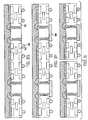
- FIGS. 4A-4Hshow one example of steps performed in assembly of embodiments of an integrated circuit package of the present invention.
- FIGS. 5A-5Ishow another example of steps performed in assembly of embodiments of an integrated circuit package of the present invention.
- FIG. 6is a simplified cross-sectional view of an integrated circuit package assembly including an integrated circuit package as shown in FIG. 2 and another integrated circuit package.
- FIGS. 1 and 2show certain components of integrated circuit packages according to embodiments of the present invention.
- the integrated circuit packages depicted in FIGS. 1 and 2each generally include a substrate 101 , a semiconductor die 103 and an encapsulant 105 .
- the substrate 101may be made of either a rigid material (e.g., BT, FR4, FR5 or ceramic) or a flexible material (e.g., polyimide), and may have circuit traces 112 onto which a semiconductor die 103 may be interconnected using, for example, wire bonding techniques or tape automated bonding.
- the packagemeasures about 1.0 mm thick (shown as dimension “a” in FIG. 1 ) and about 35 mm wide (shown as dimension “b” in FIG. 3 ).
- the width dimension of certain other embodimentsmay vary from 7 mm to 50 mm. However, such dimensions are provided only as non-limiting examples of certain embodiments of the present invention.
- external terminals of one embodiment of the present inventionmay include an array of solder balls 106 .
- the solder balls 106may function as leads capable of providing power, signal inputs and signal outputs to the semiconductor die 103 .
- Such a configurationmay be referred to as a type of ball grid array. Absent the solder balls 106 , such a configuration may be referred to as a type of land grid array, as shown in FIG. 1 .
- traces 112may be embedded photolithographically into the substrate 101 , and are electrically conductive to provide a circuit connection between the semiconductor die 103 and the substrate 101 . Such traces 112 may also provide an interconnection between input and output terminals of the semiconductor die 103 and external terminals provided on the package.
- the substrate 101 of the embodiment shown in FIG. 1may have a multi-layer circuit trace 112 made of copper.
- the substrate 101 shown in FIG. 1has vias 110 which may be drilled into it to connect the top and bottom portions of each circuit trace 112 .
- Such vias 110may be plated with copper to electrically connect the top and bottom portions of each trace 112 .
- the substrate 101 shown in FIG. 1may also have a solder mask on its surface. The solder mask of one embodiment electrically insulates the substrate and reduces wetting (i.e., reduces unwanted flow of solder into the substrate 101 ).
- One embodimentmay include a conductive trace 112 in the form of a ring around the cavity 120 in the substrate 101 .
- a ring-shaped conductive trace 112may be connected to the top surface of the substrate 101 by means of electrically conductive vias 110 .
- Such an arrangementmay allow a heat slug 108 to be electrically connected to the semiconductor die 103 by the way of wire bonding 104 , thereby resulting in a ground plane surface beneath the semiconductor die 103 , which may enhance the electrical characteristics of the package.
- FIG. 4Ashows a step in the manufacture of one type of the integrated circuit package showing a substrate 101 with a cavity 120 .
- the substrate 101may be produced in a form to accommodate standard semiconductor manufacturing equipment and process flows, and may also be configured in a matrix format to accommodate high-density package manufacturing.
- FIG. 5Adepicts a step in another process for manufacturing integrated circuit packages, and shows a substrate 501 with a number of cavities 520 - 1 , 520 - 2 .
- a tape 102 with adhesive material on at least one sideis applied to the bottom side of the substrate 101 , and may be applied in strip form to accommodate a number of substrates.
- the tape 102may be, for example, a high temperature stable polyimide with an adhesive material on at least one surface.
- FIG. 5Bdepicts a tape 502 having its adhesive material on the surface which interfaces with the bottom of the substrate 501 .
- the adhesive materialhas a contact sticking characteristic such that a semiconductor die 103 placed into contact with the adhesive material will stick to the tape 502 . In this embodiment, however, the adhesive material is such that no adhesive residue is left on the substrate 101 when the tape 502 is removed.
- FIG. 4Ca semiconductor die 103 may then be mounted or otherwise attached to the tape 102 through the cavity 120 in the substrate 101 .
- FIG. 5Cdepicts a number of semiconductor dies 503 - 1 , 503 - 2 mounted or otherwise attached to the tape 502 through each of the cavities 520 - 1 , 520 - 2 of the substrate 501 .
- the semiconductor die 103may then be interconnected to routing traces 112 of the substrate 101 by a gold thermo-sonic wire bonding technique.
- gold wires 104may interconnect the semiconductor die 103 to traces 112 of the substrate 101 .
- FIG. 5Ddepicts the semiconductor dies 503 - 1 , 503 - 2 being interconnected to routing traces by, e.g., a gold thermo-sonic wire bonding technique.
- the substrate 101 , 501may be encapsulated.
- the encapsulant material 105 , 505may be an epoxy based material applied by, for example, either a liquid molding encapsulation process or a transfer molding technique.
- the substrate 101is fully encapsulated on one side.
- the substrate 101is encapsulated only in the semiconductor die 130 and wire bond area, leaving much of the surface of the substrate 101 opposite to the solder ball area free of encapsulant material 105 .
- the tape 102 , 502may then be removed from the package subassembly as shown in FIGS. 4F and 5F .
- solder balls 106may then be attached to traces 112 of the substrate 101 using, for example, a reflow soldering process.
- FIG. 5Gdepicts solder balls 506 being attached to traces 512 of the substrate 501 .
- the solder balls 106 , 506may be made of a variety of materials including lead (Pb) free solder.
- a heat slug 108may be attached to the exposed surface of the semiconductor die 103 and the area surrounding the cavity 120 in the substrate 101 using a thermally conductive adhesive material 107 such as epoxy.
- the adhesive material 107may also be electrically conductive, such as silver-filled epoxy.
- FIG. 5Hdepicts attachment of a heat slug 508 to each semiconductor die 503 only.
- an alternative heat slugsuch as the one depicted in FIG. 4H , may also be attached to one or more semiconductor dies 503 .
- the integrated circuit packagesmay be singulated into individual units using, e.g., a saw singulation or punching technique.
- FIG. 6shows an integrated circuit package assembly according to an embodiment of the present invention.
- such an embodimentincludes two integrated circuit packages stacked one on top of the other and attached to one another by solder balls 106 .
- the integrated circuit package assembly shown in FIG. 6includes two packages of the embodiment shown in FIG. 2 and a heat slug 108 .
- Another embodiment of an integrated circuit package assembly according to the present inventionmay include two or more integrated circuit packages without a heat slug 108 .
- Other embodiments of integrated circuit package assemblies according to the present inventionmay include integrated circuit packages other than the embodiments specifically shown in FIG. 6 .
- the substrate 101 of certain embodiments of integrated circuit packages and assembliesmay contain electrically conductive traces 112 on an upper surface of the substrate 101 to facilitate electrical coupling with a second integrated circuit package.
- the heat slug 108 shown in FIG. 6may provide a thermal path between a semiconductor die 103 and the environment.
- the heat slug 108may be aligned with and positioned below the bottom surface of the semiconductor die 103 such that the heat slug 108 may contact or thermally couple with an external device such as, e.g., a printed circuit board 200 .
- the heat slug 108is preferably made of a thermally conductive material such as copper or copper alloy.
- the heat slug 108may be sized and configured for use in a specific package arrangement such that, in certain embodiments, the heat slug 108 contacts another type of external device (e.g., an integrated circuit package) to which a package is attached.
- the heat slug 108may be plated with solder or some other appropriate metal to enhance the reflow of solder to the surface of the heat slug 108 .
- the opposite side of the heat slug 108may also be oxide coated to enhance the adhesion to the encapsulant material 105 .
Landscapes
- Engineering & Computer Science (AREA)
- Microelectronics & Electronic Packaging (AREA)
- Power Engineering (AREA)
- Computer Hardware Design (AREA)
- Physics & Mathematics (AREA)
- Condensed Matter Physics & Semiconductors (AREA)
- General Physics & Mathematics (AREA)
- Manufacturing & Machinery (AREA)
- Structures Or Materials For Encapsulating Or Coating Semiconductor Devices Or Solid State Devices (AREA)
- Cooling Or The Like Of Semiconductors Or Solid State Devices (AREA)
Abstract
Description
- The present invention relates to integrated circuit packaging and manufacturing thereof, and more particularly, to integrated circuit packaging for improved dissipation of thermal energy.
- A semiconductor device generates a great deal of heat during normal operation. As the speed of semiconductors has increased, so too has the amount of heat generated by them. It is desirable to dissipate this heat from an integrated circuit package in an efficient manner.
- A heat sink is one type of device used to help dissipate heat from some integrated circuit packages. Various shapes and sizes of heat sink devices have been incorporated onto, into or around integrated circuit packages for improving heat dissipation from the particular integrated circuit package. For example, U.S. Pat. No. 5,596,231 to Combs, entitled “High Power Dissipation Plastic Encapsulated Package For Integrated Circuit Die,” discloses a selectively coated heat sink attached directly on to the integrated circuit die and to a lead frame for external electrical connections.
- In one aspect, the invention features a method of manufacturing an integrated circuit package including providing a substrate having a first surface, a second surface opposite the first surface, a cavity through the substrate between the first and second surfaces and a conductive via extending through the substrate and electrically connecting the first surface of the substrate with the second surface of the substrate, applying a strip to the second surface of the substrate, mounting a semiconductor die on the strip, at least a portion of the semiconductor die being disposed inside the cavity, encapsulating in a molding material at least a portion of the first surface of the substrate, and removing the strip from the substrate.
- In another aspect, the invention features a method of manufacturing an integrated circuit package including providing a substrate having a first surface, a second surface opposite the first surface, a plurality of cavities, each said cavity through the substrate between the first and second surfaces, and a plurality of conductive vias, each said via extending through the substrate and electrically connecting the first surface of the substrate with the second surface of the substrate, applying a strip to the second surface of said substrate, mounting a plurality of semiconductor dies on the strip, at least a portion of each semiconductor die being disposed inside each cavity, encapsulating in a molding material at least a portion of the first surface of said substrate, and removing the strip from the substrate to expose a surface of each semiconductor die.
- In a further aspect, the invention features an integrated circuit package including a substrate having a first surface, a second surface opposite the first surface, a cavity through the substrate between the first and second surfaces and a conductive via extending through the substrate and electrically connecting the first surface of the substrate with the second surface of the substrate, a semiconductor die electrically coupled with the conductive via, at least a portion of the semiconductor die being disposed inside the cavity of the substrate, an encapsulant material encapsulating a portion of the semiconductor die such that at least a portion of a surface of the semiconductor die is exposed.
- The foregoing features and other aspects of the invention are explained in the following description taken in connection with the accompanying drawings, wherein:
FIG. 1 is a simplified cross-sectional view of an integrated circuit package according to one embodiment of the present invention;FIG. 2 is a simplified cross-sectional view of an integrated circuit package according to a second embodiment of the present invention;FIG. 3 is a simplified bottom view of an integrated circuit package according to embodiments of the present invention;FIGS. 4A-4H show one example of steps performed in assembly of embodiments of an integrated circuit package of the present invention.FIGS. 5A-5I show another example of steps performed in assembly of embodiments of an integrated circuit package of the present invention.FIG. 6 is a simplified cross-sectional view of an integrated circuit package assembly including an integrated circuit package as shown inFIG. 2 and another integrated circuit package.- Various embodiments of the integrated circuit package and various examples of methods for manufacturing integrated circuit packages according to the present invention will now be described with reference to the drawings.
FIGS. 1 and 2 show certain components of integrated circuit packages according to embodiments of the present invention. The integrated circuit packages depicted inFIGS. 1 and 2 each generally include asubstrate 101, asemiconductor die 103 and anencapsulant 105. Thesubstrate 101 may be made of either a rigid material (e.g., BT, FR4, FR5 or ceramic) or a flexible material (e.g., polyimide), and may havecircuit traces 112 onto which asemiconductor die 103 may be interconnected using, for example, wire bonding techniques or tape automated bonding. In the embodiment shown inFIG. 1 , the package measures about 1.0 mm thick (shown as dimension “a” inFIG. 1 ) and about 35 mm wide (shown as dimension “b” inFIG. 3 ). The width dimension of certain other embodiments may vary from 7 mm to 50 mm. However, such dimensions are provided only as non-limiting examples of certain embodiments of the present invention.- As shown in
FIG. 2 , external terminals of one embodiment of the present invention may include an array ofsolder balls 106. In such an embodiment, thesolder balls 106 may function as leads capable of providing power, signal inputs and signal outputs to thesemiconductor die 103. Such a configuration may be referred to as a type of ball grid array. Absent thesolder balls 106, such a configuration may be referred to as a type of land grid array, as shown inFIG. 1 . - In one embodiment,
traces 112 may be embedded photolithographically into thesubstrate 101, and are electrically conductive to provide a circuit connection between thesemiconductor die 103 and thesubstrate 101.Such traces 112 may also provide an interconnection between input and output terminals of the semiconductor die103 and external terminals provided on the package. In particular, thesubstrate 101 of the embodiment shown inFIG. 1 may have amulti-layer circuit trace 112 made of copper. Thesubstrate 101 shown inFIG. 1 hasvias 110 which may be drilled into it to connect the top and bottom portions of eachcircuit trace 112.Such vias 110 may be plated with copper to electrically connect the top and bottom portions of eachtrace 112. Thesubstrate 101 shown inFIG. 1 may also have a solder mask on its surface. The solder mask of one embodiment electrically insulates the substrate and reduces wetting (i.e., reduces unwanted flow of solder into the substrate101). - As shown in
FIGS. 1-3 , thesubstrate 101 is designed with acavity 120 made through the base material with sufficient clearance to accommodate the specific size ofsemiconductor die 103 used in the package. - One embodiment may include a
conductive trace 112 in the form of a ring around thecavity 120 in thesubstrate 101. Such a ring-shapedconductive trace 112 may be connected to the top surface of thesubstrate 101 by means of electricallyconductive vias 110. Such an arrangement may allow aheat slug 108 to be electrically connected to thesemiconductor die 103 by the way ofwire bonding 104, thereby resulting in a ground plane surface beneath thesemiconductor die 103, which may enhance the electrical characteristics of the package. - In a preferred embodiment shown in
FIG. 2 , theencapsulant material 105 does not extend to the package edge. In such an embodiment, electricallyconductive vias 110 connecttraces 112 from the top surface of the package tocorresponding pads 113 on the side of the package opposite to the solder ball attachment. - Example methods of manufacturing embodiments of the integrated circuit packages will now be described with reference to the drawings, in particular,
FIGS. 4A-4H andFIGS. 5A-5I .FIG. 4A shows a step in the manufacture of one type of the integrated circuit package showing asubstrate 101 with acavity 120. Thesubstrate 101 may be produced in a form to accommodate standard semiconductor manufacturing equipment and process flows, and may also be configured in a matrix format to accommodate high-density package manufacturing.FIG. 5A depicts a step in another process for manufacturing integrated circuit packages, and shows asubstrate 501 with a number of cavities520-1,520-2. - As shown in
FIG. 4B , atape 102 with adhesive material on at least one side is applied to the bottom side of thesubstrate 101, and may be applied in strip form to accommodate a number of substrates. Thetape 102 may be, for example, a high temperature stable polyimide with an adhesive material on at least one surface.FIG. 5B depicts a tape502 having its adhesive material on the surface which interfaces with the bottom of thesubstrate 501. In one embodiment, the adhesive material has a contact sticking characteristic such that asemiconductor die 103 placed into contact with the adhesive material will stick to the tape502. In this embodiment, however, the adhesive material is such that no adhesive residue is left on thesubstrate 101 when the tape502 is removed. - As shown in
FIG. 4C , asemiconductor die 103 may then be mounted or otherwise attached to thetape 102 through thecavity 120 in thesubstrate 101.FIG. 5C depicts a number of semiconductor dies503-1,503-2 mounted or otherwise attached to the tape502 through each of the cavities520-1,520-2 of thesubstrate 501. - As shown in
FIG. 4D , the semiconductor die103 may then be interconnected to routing traces112 of thesubstrate 101 by a gold thermo-sonic wire bonding technique. In such an embodiment,gold wires 104 may interconnect the semiconductor die103 totraces 112 of thesubstrate 101.FIG. 5D depicts the semiconductor dies503-1,503-2 being interconnected to routing traces by, e.g., a gold thermo-sonic wire bonding technique. - As shown in
FIGS. 4E and 5E , after wire bonding, thesubstrate encapsulant material FIG. 1 , thesubstrate 101 is fully encapsulated on one side. To manufacture another embodiment of an integrated circuit package (shown inFIG. 2 ), thesubstrate 101 is encapsulated only in the semiconductor die130 and wire bond area, leaving much of the surface of thesubstrate 101 opposite to the solder ball area free ofencapsulant material 105. After an encapsulation process, thetape 102,502 may then be removed from the package subassembly as shown inFIGS. 4F and 5F . - As shown in
FIG. 4G ,solder balls 106 may then be attached totraces 112 of thesubstrate 101 using, for example, a reflow soldering process. In another example method of manufacture,FIG. 5G depictssolder balls 506 being attached totraces 512 of thesubstrate 501. Thesolder balls - As shown in
FIG. 4H , after solder ball attachment, aheat slug 108 may be attached to the exposed surface of the semiconductor die103 and the area surrounding thecavity 120 in thesubstrate 101 using a thermally conductive adhesive material107 such as epoxy. The adhesive material107, may also be electrically conductive, such as silver-filled epoxy.FIG. 5H depicts attachment of aheat slug 508 to each semiconductor die503 only. However, an alternative heat slug, such as the one depicted inFIG. 4H , may also be attached to one or more semiconductor dies503. - As shown in
FIG. 5I , after such heat slug attachment, the integrated circuit packages may be singulated into individual units using, e.g., a saw singulation or punching technique. FIG. 6 shows an integrated circuit package assembly according to an embodiment of the present invention. As depicted inFIG. 6 , such an embodiment includes two integrated circuit packages stacked one on top of the other and attached to one another bysolder balls 106. The integrated circuit package assembly shown inFIG. 6 includes two packages of the embodiment shown inFIG. 2 and aheat slug 108. Another embodiment of an integrated circuit package assembly according to the present invention may include two or more integrated circuit packages without aheat slug 108. Other embodiments of integrated circuit package assemblies according to the present invention may include integrated circuit packages other than the embodiments specifically shown inFIG. 6 . As shown inFIGS. 1, 2 , and6, thesubstrate 101 of certain embodiments of integrated circuit packages and assemblies may contain electricallyconductive traces 112 on an upper surface of thesubstrate 101 to facilitate electrical coupling with a second integrated circuit package.- The
heat slug 108 shown inFIG. 6 may provide a thermal path between asemiconductor die 103 and the environment. In the embodiment shown inFIG. 6 , theheat slug 108 may be aligned with and positioned below the bottom surface of the semiconductor die103 such that theheat slug 108 may contact or thermally couple with an external device such as, e.g., a printedcircuit board 200. Theheat slug 108 is preferably made of a thermally conductive material such as copper or copper alloy. Theheat slug 108 may be sized and configured for use in a specific package arrangement such that, in certain embodiments, theheat slug 108 contacts another type of external device (e.g., an integrated circuit package) to which a package is attached. Theheat slug 108 may be plated with solder or some other appropriate metal to enhance the reflow of solder to the surface of theheat slug 108. The opposite side of theheat slug 108 may also be oxide coated to enhance the adhesion to theencapsulant material 105. - Although specific embodiments of integrated circuit packages, integrated circuit package assemblies, and methods of manufacturing integrated circuit packages have been shown and described, it is to be understood that there are other embodiments which are equivalent to the described embodiments. Moreover, although a particular order of certain manufacturing steps has been discussed, it is to be understood that aspects of the invention are not limited to the particular order disclosed. The scope of the invention is not to be limited by the specific embodiments and examples depicted and described herein, but only by the claims.
Claims (21)
1-22. (canceled)
23. An integrated circuit package, comprising:
a substrate comprising:
a first surface,
a second surface opposite said first surface,
a cavity through said substrate between said first and second surfaces, and
a conductive via extending through said substrate and electrically connecting said first surface of said substrate with said second surface of said substrate;
a semiconductor die electrically coupled with said conductive via at said first surface of said substrate, at least a portion of said semiconductor die being disposed inside said cavity of said substrate;
an encapsulant material encapsulating a portion of said semiconductor die such that at least a portion of a surface of said semiconductor die is exposed; and
a heat slug thermally and electrically coupled with said semiconductor die, wherein said conductive via is further electrically coupled with said heat slug to provide a ground connection for said semiconductor die at said first surface of said substrate.
24. The integrated circuit package ofclaim 23 , further comprising a conductive member adapted for attachment of said integrated circuit package to an external device.
25. The integrated circuit package ofclaim 24 , said conductive member attached to said first surface of said substrate.
26. The integrated circuit package ofclaim 23 , further comprising at least one wire electrically coupling said semiconductor die with said conductive via.
27. The integrated circuit package ofclaim 23 , at least a portion of said first surface of said substrate being adapted for coupling said integrated circuit package with a second integrated circuit package.
28. The integrated circuit package ofclaim 23 , said substrate further comprising a multi-layer trace embedded therein.
29. An integrated circuit package assembly comprising the integrated circuit package ofclaim 23 attached to at least one other integrated circuit package.
30. The integrated circuit package assembly ofclaim 29 , wherein one of said integrated circuit packages is stacked on top of at least one of the other of said integrated circuit packages.
31. The integrated circuit package ofclaim 25 , further comprising a second conductive member attached to said second surface of said substrate.
32. The integrated circuit package ofclaim 23 , said package having a thickness dimension of about one millimeter.
33. The integrated circuit package ofclaim 39 , said package having a width dimension of about seven millimeters.
34. The integrated circuit package ofclaim 23 , said substrate being substantially planar and said semiconductor die being aligned in a plane with said substrate.
35. The integrated circuit package ofclaim 23 , said integrated circuit package being a land grid array.
36. The integrated circuit package ofclaim 23 said integrated circuit package being a ball grid array.
37. The integrated circuit package ofclaim 23 , said encapsulant material comprising an epoxy.
38. The integrated circuit package ofclaim 23 , further comprising a ring-like trace embedded in said substrate.
39. The integrated circuit package ofclaim 33 , said package having a width dimension of about 7 mm to 50 mm inclusively.
40. An integrated circuit package, comprising:
a substrate comprising:
a first surface,
a second surface opposite said first surface,
a cavity through said substrate between said first and second surfaces, and
means for electrically connecting said first surface of said substrate with said second surface of said substrate;
a semiconductor die, at least a portion of which is disposed inside said cavity of said substrate;
an encapsulant material encapsulating a portion of said semiconductor die such that at least a portion of a surface of said semiconductor die is exposed; and
means for thermally coupling said semiconductor die to a printed circuit board, wherein said means for thermally coupling is electrically coupled with said means for electrically connecting said first surface of said substrate with said second surface of said substrate to provide a ground connection for said semiconductor die at said first surface of said substrate.
41. An integrated circuit package assembly comprising the integrated circuit package ofclaim 40 attached to at least one other integrated circuit package.
42. The integrated circuit package assembly ofclaim 41 , wherein one of said integrated circuit packages is stacked on top of at least one of the other of said integrated circuit packages.
Priority Applications (1)
| Application Number | Priority Date | Filing Date | Title |
|---|---|---|---|
| US10/635,839US20050077613A1 (en) | 2002-01-31 | 2003-08-06 | Integrated circuit package |
Applications Claiming Priority (2)
| Application Number | Priority Date | Filing Date | Title |
|---|---|---|---|
| US10/062,650US6790710B2 (en) | 2002-01-31 | 2002-01-31 | Method of manufacturing an integrated circuit package |
| US10/635,839US20050077613A1 (en) | 2002-01-31 | 2003-08-06 | Integrated circuit package |
Related Parent Applications (1)
| Application Number | Title | Priority Date | Filing Date |
|---|---|---|---|
| US10/062,650DivisionUS6790710B2 (en) | 2001-08-15 | 2002-01-31 | Method of manufacturing an integrated circuit package |
Publications (1)
| Publication Number | Publication Date |
|---|---|
| US20050077613A1true US20050077613A1 (en) | 2005-04-14 |
Family
ID=27610333
Family Applications (2)
| Application Number | Title | Priority Date | Filing Date |
|---|---|---|---|
| US10/062,650Expired - LifetimeUS6790710B2 (en) | 2001-08-15 | 2002-01-31 | Method of manufacturing an integrated circuit package |
| US10/635,839AbandonedUS20050077613A1 (en) | 2002-01-31 | 2003-08-06 | Integrated circuit package |
Family Applications Before (1)
| Application Number | Title | Priority Date | Filing Date |
|---|---|---|---|
| US10/062,650Expired - LifetimeUS6790710B2 (en) | 2001-08-15 | 2002-01-31 | Method of manufacturing an integrated circuit package |
Country Status (1)
| Country | Link |
|---|---|
| US (2) | US6790710B2 (en) |
Cited By (30)
| Publication number | Priority date | Publication date | Assignee | Title |
|---|---|---|---|---|
| US20040262754A1 (en)* | 2002-02-01 | 2004-12-30 | Khan Reza-Ur Rahman | IC die support structures for ball grid array package fabrication |
| US20060273458A1 (en)* | 2005-06-07 | 2006-12-07 | Wen-Shien Huang | Substrate structure of semiconductor package |
| US20100127363A1 (en)* | 2006-04-28 | 2010-05-27 | Utac Thai Limited | Very extremely thin semiconductor package |
| US7790512B1 (en) | 2007-11-06 | 2010-09-07 | Utac Thai Limited | Molded leadframe substrate semiconductor package |
| US20100230802A1 (en)* | 2009-03-12 | 2010-09-16 | Utac Thai Limited | Metallic solderability preservation coating on metal part of semiconductor package to prevent oxide |
| US20100311208A1 (en)* | 2008-05-22 | 2010-12-09 | Utac Thai Limited | Method and apparatus for no lead semiconductor package |
| US20100327432A1 (en)* | 2006-09-26 | 2010-12-30 | Utac Thai Limited | Package with heat transfer |
| US20110039371A1 (en)* | 2008-09-04 | 2011-02-17 | Utac Thai Limited | Flip chip cavity package |
| US20110133319A1 (en)* | 2009-12-04 | 2011-06-09 | Utac Thai Limited | Auxiliary leadframe member for stabilizing the bond wire process |
| US20110147931A1 (en)* | 2006-04-28 | 2011-06-23 | Utac Thai Limited | Lead frame land grid array with routing connector trace under unit |
| US20110198752A1 (en)* | 2006-04-28 | 2011-08-18 | Utac Thai Limited | Lead frame ball grid array with traces under die |
| US8013437B1 (en) | 2006-09-26 | 2011-09-06 | Utac Thai Limited | Package with heat transfer |
| US20110221051A1 (en)* | 2010-03-11 | 2011-09-15 | Utac Thai Limited | Leadframe based multi terminal ic package |
| US8076184B1 (en)* | 2010-08-16 | 2011-12-13 | Stats Chippac, Ltd. | Semiconductor device and method of forming wafer-level multi-row etched leadframe with base leads and embedded semiconductor die |
| US8461694B1 (en) | 2006-04-28 | 2013-06-11 | Utac Thai Limited | Lead frame ball grid array with traces under die having interlocking features |
| US8460970B1 (en) | 2006-04-28 | 2013-06-11 | Utac Thai Limited | Lead frame ball grid array with traces under die having interlocking features |
| US8871571B2 (en) | 2010-04-02 | 2014-10-28 | Utac Thai Limited | Apparatus for and methods of attaching heat slugs to package tops |
| US9000590B2 (en) | 2012-05-10 | 2015-04-07 | Utac Thai Limited | Protruding terminals with internal routing interconnections semiconductor device |
| US9006034B1 (en) | 2012-06-11 | 2015-04-14 | Utac Thai Limited | Post-mold for semiconductor package having exposed traces |
| US9082607B1 (en) | 2006-12-14 | 2015-07-14 | Utac Thai Limited | Molded leadframe substrate semiconductor package |
| CN104810327A (en)* | 2014-01-27 | 2015-07-29 | 联发科技股份有限公司 | Chip package structure and method for forming same |
| US9355940B1 (en) | 2009-12-04 | 2016-05-31 | Utac Thai Limited | Auxiliary leadframe member for stabilizing the bond wire process |
| US9449900B2 (en) | 2009-07-23 | 2016-09-20 | UTAC Headquarters Pte. Ltd. | Leadframe feature to minimize flip-chip semiconductor die collapse during flip-chip reflow |
| US9449905B2 (en) | 2012-05-10 | 2016-09-20 | Utac Thai Limited | Plated terminals with routing interconnections semiconductor device |
| US9466545B1 (en) | 2007-02-21 | 2016-10-11 | Amkor Technology, Inc. | Semiconductor package in package |
| US9761435B1 (en) | 2006-12-14 | 2017-09-12 | Utac Thai Limited | Flip chip cavity package |
| US9805955B1 (en) | 2015-11-10 | 2017-10-31 | UTAC Headquarters Pte. Ltd. | Semiconductor package with multiple molding routing layers and a method of manufacturing the same |
| US10242953B1 (en) | 2015-05-27 | 2019-03-26 | Utac Headquarters PTE. Ltd | Semiconductor package with plated metal shielding and a method thereof |
| US10242934B1 (en) | 2014-05-07 | 2019-03-26 | Utac Headquarters Pte Ltd. | Semiconductor package with full plating on contact side surfaces and methods thereof |
| US10276477B1 (en) | 2016-05-20 | 2019-04-30 | UTAC Headquarters Pte. Ltd. | Semiconductor package with multiple stacked leadframes and a method of manufacturing the same |
Families Citing this family (35)
| Publication number | Priority date | Publication date | Assignee | Title |
|---|---|---|---|---|
| JP3602968B2 (en)* | 1998-08-18 | 2004-12-15 | 沖電気工業株式会社 | Semiconductor device and substrate connection structure thereof |
| US6982485B1 (en)* | 2002-02-13 | 2006-01-03 | Amkor Technology, Inc. | Stacking structure for semiconductor chips and a semiconductor package using it |
| US7042072B1 (en)* | 2002-08-02 | 2006-05-09 | Amkor Technology, Inc. | Semiconductor package and method of manufacturing the same which reduces warpage |
| US20040212081A1 (en)* | 2003-04-08 | 2004-10-28 | Carberry Patrick J. | Process for fabricating a power hybrid module |
| US7205649B2 (en)* | 2003-06-30 | 2007-04-17 | Intel Corporation | Ball grid array copper balancing |
| TWI239083B (en)* | 2004-02-26 | 2005-09-01 | Advanced Semiconductor Eng | Chip package structure |
| US7008820B2 (en)* | 2004-06-10 | 2006-03-07 | St Assembly Test Services Ltd. | Chip scale package with open substrate |
| US8319313B1 (en) | 2004-10-26 | 2012-11-27 | Marvell Israel (M.I.S.L) Ltd. | Circuits, systems, and methods for reducing effects of cross talk in I/O lines and wire bonds |
| US20060108676A1 (en)* | 2004-11-22 | 2006-05-25 | Punzalan Nelson V Jr | Multi-chip package using an interposer |
| TWI246760B (en)* | 2004-12-22 | 2006-01-01 | Siliconware Precision Industries Co Ltd | Heat dissipating semiconductor package and fabrication method thereof |
| US7456655B1 (en) | 2005-05-16 | 2008-11-25 | Marvell Israel (Misl) Ltd. | System and process for overcoming wire-bond originated cross-talk |
| US7656173B1 (en)* | 2006-04-27 | 2010-02-02 | Utac Thai Limited | Strip socket having a recessed portions in the base to accept bottom surface of packaged semiconductor devices mounted on a leadframe for testing and burn-in |
| DE102006030581B3 (en)* | 2006-07-03 | 2008-02-21 | Infineon Technologies Ag | Method for producing a component |
| US20080123318A1 (en)* | 2006-11-08 | 2008-05-29 | Atmel Corporation | Multi-component electronic package with planarized embedded-components substrate |
| TW200839994A (en)* | 2007-03-16 | 2008-10-01 | Phoenix Prec Technology Corp | Packing structure and stacked structure using thereof |
| US7569421B2 (en)* | 2007-05-04 | 2009-08-04 | Stats Chippac, Ltd. | Through-hole via on saw streets |
| US7829998B2 (en) | 2007-05-04 | 2010-11-09 | Stats Chippac, Ltd. | Semiconductor wafer having through-hole vias on saw streets with backside redistribution layer |
| US7723159B2 (en)* | 2007-05-04 | 2010-05-25 | Stats Chippac, Ltd. | Package-on-package using through-hole via die on saw streets |
| US8445325B2 (en) | 2007-05-04 | 2013-05-21 | Stats Chippac, Ltd. | Package-in-package using through-hole via die on saw streets |
| FR2926890B1 (en)* | 2008-01-30 | 2011-01-07 | St Microelectronics Grenoble | METHOD AND DEVICE FOR TRANSPORTING ELECTRONIC MODULES AND EQUIPMENT FOR HANDLING AND TESTING ELECTRONIC MODULES |
| US8188379B2 (en)* | 2008-07-04 | 2012-05-29 | Unimicron Technology Corp. | Package substrate structure |
| US20100019374A1 (en)* | 2008-07-25 | 2010-01-28 | Stmicroelectronics, Inc. | Ball grid array package |
| US7989950B2 (en)* | 2008-08-14 | 2011-08-02 | Stats Chippac Ltd. | Integrated circuit packaging system having a cavity |
| US8334764B1 (en) | 2008-12-17 | 2012-12-18 | Utac Thai Limited | Method and apparatus to prevent double semiconductor units in test socket |
| WO2011036840A1 (en)* | 2009-09-24 | 2011-03-31 | パナソニック株式会社 | Semiconductor device, semiconductor package, and method for manufacturing semiconductor device |
| US9548251B2 (en)* | 2012-01-12 | 2017-01-17 | Broadcom Corporation | Semiconductor interposer having a cavity for intra-interposer die |
| US9059157B2 (en)* | 2012-06-04 | 2015-06-16 | Stats Chippac Ltd. | Integrated circuit packaging system with substrate and method of manufacture thereof |
| CN103700656A (en)* | 2012-09-27 | 2014-04-02 | 国碁电子(中山)有限公司 | Thick film hybrid circuit structure and manufacturing method |
| US8980691B2 (en)* | 2013-06-28 | 2015-03-17 | Stats Chippac, Ltd. | Semiconductor device and method of forming low profile 3D fan-out package |
| FR3015111B1 (en)* | 2013-12-16 | 2017-08-25 | Centre Nat D'etudes Spatiales C N E S | METHOD AND DEVICE FOR PREPARING AN INTEGRATED CIRCUIT DIAGNOSTIC SAMPLE |
| FR3063862B1 (en)* | 2017-03-08 | 2021-05-28 | Wisekey Semiconductors | ARRANGEMENT TO TEST THE BEHAVIOR OF CHIPS TO LASER ATTACKS FROM THE REAR PANEL |
| CN110446369A (en)* | 2019-07-23 | 2019-11-12 | 中国科学技术大学 | Bonding structure, bonding method and the Package boxes comprising the bonding structure |
| CN110446368B (en)* | 2019-07-23 | 2024-07-26 | 中国科学技术大学 | Bonding structure, bonding method and packaging box containing bonding structure |
| CN113506782A (en)* | 2021-06-21 | 2021-10-15 | 日月光半导体制造股份有限公司 | Semiconductor structure and method of making the same |
| CN113506783B (en)* | 2021-06-29 | 2025-10-03 | 日月光半导体制造股份有限公司 | Semiconductor structure and method for manufacturing the same |
Citations (95)
| Publication number | Priority date | Publication date | Assignee | Title |
|---|---|---|---|---|
| US3908075A (en)* | 1971-11-20 | 1975-09-23 | Ferranti Ltd | Lead frame support for semiconductor devices |
| US3942245A (en)* | 1971-11-20 | 1976-03-09 | Ferranti Limited | Related to the manufacture of lead frames and the mounting of semiconductor devices thereon |
| US4501960A (en)* | 1981-06-22 | 1985-02-26 | Motorola, Inc. | Micropackage for identification card |
| US4674175A (en)* | 1985-04-02 | 1987-06-23 | Eta Sa Fabrique D'ebauches | Process for manufacturing electronic modules for microcircuit cards |
| US5023202A (en)* | 1989-07-14 | 1991-06-11 | Lsi Logic Corporation | Rigid strip carrier for integrated circuits |
| US5041395A (en)* | 1989-04-07 | 1991-08-20 | Sgs-Thomson Microelectronics S.A. | Method of encapsulating an integrated circuit using a punched metal grid attached to a perforated dielectric strip |
| US5122860A (en)* | 1987-08-26 | 1992-06-16 | Matsushita Electric Industrial Co., Ltd. | Integrated circuit device and manufacturing method thereof |
| US5200362A (en)* | 1989-09-06 | 1993-04-06 | Motorola, Inc. | Method of attaching conductive traces to an encapsulated semiconductor die using a removable transfer film |
| US5285352A (en)* | 1992-07-15 | 1994-02-08 | Motorola, Inc. | Pad array semiconductor device with thermal conductor and process for making the same |
| US5285105A (en)* | 1988-12-07 | 1994-02-08 | Tribotech | Semiconductor die packages having lead support frame |
| US5334857A (en)* | 1992-04-06 | 1994-08-02 | Motorola, Inc. | Semiconductor device with test-only contacts and method for making the same |
| US5397921A (en)* | 1993-09-03 | 1995-03-14 | Advanced Semiconductor Assembly Technology | Tab grid array |
| US5420460A (en)* | 1993-08-05 | 1995-05-30 | Vlsi Technology, Inc. | Thin cavity down ball grid array package based on wirebond technology |
| US5435057A (en)* | 1990-10-30 | 1995-07-25 | International Business Machines Corporation | Interconnection method and structure for organic circuit boards |
| US5482736A (en)* | 1994-08-04 | 1996-01-09 | Amkor Electronics, Inc. | Method for applying flux to ball grid array package |
| US5482898A (en)* | 1993-04-12 | 1996-01-09 | Amkor Electronics, Inc. | Method for forming a semiconductor device having a thermal dissipator and electromagnetic shielding |
| US5521432A (en)* | 1991-10-14 | 1996-05-28 | Fujitsu Limited | Semiconductor device having improved leads comprising palladium plated nickel |
| US5556807A (en)* | 1992-02-18 | 1996-09-17 | Intel Corporation | Advance multilayer molded plastic package using mesic technology |
| US5594275A (en)* | 1993-11-18 | 1997-01-14 | Samsung Electronics Co., Ltd. | J-leaded semiconductor package having a plurality of stacked ball grid array packages |
| US5596485A (en)* | 1995-03-16 | 1997-01-21 | Amkor Electronics, Inc. | Plastic packaged integrated circuit with heat spreader |
| US5596231A (en)* | 1991-08-05 | 1997-01-21 | Asat, Limited | High power dissipation plastic encapsulated package for integrated circuit die |
| US5620928A (en)* | 1995-05-11 | 1997-04-15 | National Semiconductor Corporation | Ultra thin ball grid array using a flex tape or printed wiring board substrate and method |
| US5641997A (en)* | 1993-09-14 | 1997-06-24 | Kabushiki Kaisha Toshiba | Plastic-encapsulated semiconductor device |
| US5642261A (en)* | 1993-12-20 | 1997-06-24 | Sgs-Thomson Microelectronics, Inc. | Ball-grid-array integrated circuit package with solder-connected thermal conductor |
| US5663593A (en)* | 1995-10-17 | 1997-09-02 | National Semiconductor Corporation | Ball grid array package with lead frame |
| US5672909A (en)* | 1995-02-07 | 1997-09-30 | Amkor Electronics, Inc. | Interdigitated wirebond programmable fixed voltage planes |
| US5710064A (en)* | 1994-08-16 | 1998-01-20 | Samsung Electronics Co., Ltd. | Method for manufacturing a semiconductor package |
| US5796170A (en)* | 1996-02-15 | 1998-08-18 | Northern Telecom Limited | Ball grid array (BGA) integrated circuit packages |
| US5796163A (en)* | 1997-05-23 | 1998-08-18 | Amkor Technology, Inc. | Solder ball joint |
| US5796038A (en)* | 1997-06-16 | 1998-08-18 | Vlsi Technology, Inc. | Technique to produce cavity-up HBGA packages |
| US5805419A (en)* | 1995-05-12 | 1998-09-08 | Stmicroelectronics, Inc. | Low-profile socketed packaging system with land-grid array and thermally conductive slug |
| US5814883A (en)* | 1995-10-04 | 1998-09-29 | Mitsubishi Denki Kabushiki Kaisha | Packaged semiconductor chip |
| US5859471A (en)* | 1992-11-17 | 1999-01-12 | Shinko Electric Industries Co., Ltd. | Semiconductor device having tab tape lead frame with reinforced outer leads |
| US5867368A (en)* | 1997-09-09 | 1999-02-02 | Amkor Technology, Inc. | Mounting for a semiconductor integrated circuit device |
| US5877043A (en)* | 1996-02-01 | 1999-03-02 | International Business Machines Corporation | Electronic package with strain relief means and method of making |
| US5886397A (en)* | 1996-09-05 | 1999-03-23 | International Rectifier Corporation | Crushable bead on lead finger side surface to improve moldability |
| US5884396A (en)* | 1997-05-01 | 1999-03-23 | Compeq Manufacturing Company, Limited | Transfer flat type ball grid array method for manufacturing packaging substrate |
| US5894108A (en)* | 1997-02-11 | 1999-04-13 | National Semiconductor Corporation | Plastic package with exposed die |
| US5900676A (en)* | 1996-08-19 | 1999-05-04 | Samsung Electronics Co., Ltd. | Semiconductor device package structure having column leads and a method for production thereof |
| US5903052A (en)* | 1998-05-12 | 1999-05-11 | Industrial Technology Research Institute | Structure for semiconductor package for improving the efficiency of spreading heat |
| US5920117A (en)* | 1994-08-02 | 1999-07-06 | Fujitsu Limited | Semiconductor device and method of forming the device |
| US5939784A (en)* | 1997-09-09 | 1999-08-17 | Amkor Technology, Inc. | Shielded surface acoustical wave package |
| US5949655A (en)* | 1997-09-09 | 1999-09-07 | Amkor Technology, Inc. | Mounting having an aperture cover with adhesive locking feature for flip chip optical integrated circuit device |
| US5950074A (en)* | 1997-04-18 | 1999-09-07 | Amkor Technology, Inc. | Method of making an integrated circuit package |
| US6011694A (en)* | 1996-08-01 | 2000-01-04 | Fuji Machinery Mfg. & Electronics Co., Ltd. | Ball grid array semiconductor package with solder ball openings in an insulative base |
| US6015722A (en)* | 1997-10-14 | 2000-01-18 | Gore Enterprise Holdings, Inc. | Method for assembling an integrated circuit chip package having an underfill material between a chip and a substrate |
| US6034427A (en)* | 1998-01-28 | 2000-03-07 | Prolinx Labs Corporation | Ball grid array structure and method for packaging an integrated circuit chip |
| US6043559A (en)* | 1996-09-09 | 2000-03-28 | Intel Corporation | Integrated circuit package which contains two in plane voltage busses and a wrap around conductive strip that connects a bond finger to one of the busses |
| US6060777A (en)* | 1998-07-21 | 2000-05-09 | Intel Corporation | Underside heat slug for ball grid array packages |
| US6072233A (en)* | 1998-05-04 | 2000-06-06 | Micron Technology, Inc. | Stackable ball grid array package |
| US6081029A (en)* | 1998-03-12 | 2000-06-27 | Matsushita Electronics Corporation | Resin encapsulated semiconductor device having a reduced thickness and improved reliability |
| USRE36773E (en)* | 1993-10-18 | 2000-07-11 | Motorola, Inc. | Method for plating using nested plating buses and semiconductor device having the same |
| US6091603A (en)* | 1999-09-30 | 2000-07-18 | International Business Machines Corporation | Customizable lid for improved thermal performance of modules using flip chips |
| US6092281A (en)* | 1998-08-28 | 2000-07-25 | Amkor Technology, Inc. | Electromagnetic interference shield driver and method |
| US6093960A (en)* | 1999-06-11 | 2000-07-25 | Advanced Semiconductor Engineering, Inc. | Semiconductor package having a heat spreader capable of preventing being soldered and enhancing adhesion and electrical performance |
| US6104086A (en)* | 1997-05-20 | 2000-08-15 | Nec Corporation | Semiconductor device having lead terminals bent in J-shape |
| US6111324A (en)* | 1998-02-05 | 2000-08-29 | Asat, Limited | Integrated carrier ring/stiffener and method for manufacturing a flexible integrated circuit package |
| US6117705A (en)* | 1997-04-18 | 2000-09-12 | Amkor Technology, Inc. | Method of making integrated circuit package having adhesive bead supporting planar lid above planar substrate |
| US6117193A (en)* | 1999-10-20 | 2000-09-12 | Amkor Technology, Inc. | Optical sensor array mounting and alignment |
| US6172419B1 (en)* | 1998-02-24 | 2001-01-09 | Micron Technology, Inc. | Low profile ball grid array package |
| US6175497B1 (en)* | 1998-09-30 | 2001-01-16 | World Wiser Electronics Inc. | Thermal vias-provided cavity-down IC package structure |
| US6184463B1 (en)* | 1998-04-13 | 2001-02-06 | Harris Corporation | Integrated circuit package for flip chip |
| US6188127B1 (en)* | 1995-02-24 | 2001-02-13 | Nec Corporation | Semiconductor packing stack module and method of producing the same |
| US6198163B1 (en)* | 1999-10-18 | 2001-03-06 | Amkor Technology, Inc. | Thin leadframe-type semiconductor package having heat sink with recess and exposed surface |
| US6201266B1 (en)* | 1999-07-01 | 2001-03-13 | Oki Electric Industry Co., Ltd. | Semiconductor device and method for manufacturing the same |
| US6201292B1 (en)* | 1997-04-02 | 2001-03-13 | Dai Nippon Insatsu Kabushiki Kaisha | Resin-sealed semiconductor device, circuit member used therefor |
| US6214644B1 (en)* | 2000-06-30 | 2001-04-10 | Amkor Technology, Inc. | Flip-chip micromachine package fabrication method |
| US6215180B1 (en)* | 1999-03-17 | 2001-04-10 | First International Computer Inc. | Dual-sided heat dissipating structure for integrated circuit package |
| US6229200B1 (en)* | 1998-06-10 | 2001-05-08 | Asat Limited | Saw-singulated leadless plastic chip carrier |
| US6228676B1 (en)* | 1996-10-31 | 2001-05-08 | Amkor Technology, Inc. | Near chip size integrated circuit package |
| US20010000924A1 (en)* | 1993-09-03 | 2001-05-10 | Marcos Karnezos | Molded plastic package with heat sink and enhanced electrical performance |
| US6236568B1 (en)* | 1999-03-20 | 2001-05-22 | Siliconware Precision Industries, Co., Ltd. | Heat-dissipating structure for integrated circuit package |
| US6239496B1 (en)* | 1999-01-18 | 2001-05-29 | Kabushiki Kaisha Toshiba | Package having very thin semiconductor chip, multichip module assembled by the package, and method for manufacturing the same |
| US6246566B1 (en)* | 1999-02-08 | 2001-06-12 | Amkor Technology, Inc. | Electrostatic discharge protection package and method |
| US6246115B1 (en)* | 1998-10-21 | 2001-06-12 | Siliconware Precision Industries Co., Ltd. | Semiconductor package having a heat sink with an exposed surface |
| US6249052B1 (en)* | 1998-06-01 | 2001-06-19 | Paul T. Lin | Substrate on chip (SOC) multiple-chip module (MCM) with chip-size-package (CSP) ready configuration |
| US6259154B1 (en)* | 1998-04-21 | 2001-07-10 | Nec Corporation | Semiconductor device and method of manufacturing the same |
| US6258629B1 (en)* | 1999-08-09 | 2001-07-10 | Amkor Technology, Inc. | Electronic device package and leadframe and method for making the package |
| US6265771B1 (en)* | 1999-01-27 | 2001-07-24 | International Business Machines Corporation | Dual chip with heat sink |
| US6266197B1 (en)* | 1999-12-08 | 2001-07-24 | Amkor Technology, Inc. | Molded window array for image sensor packages |
| US6274927B1 (en)* | 1999-06-03 | 2001-08-14 | Amkor Technology, Inc. | Plastic package for an optical integrated circuit device and method of making |
| US6278190B1 (en)* | 1999-03-04 | 2001-08-21 | Mitsubishi Denki Kabushiki Kaisha | Semiconductor device |
| US6281568B1 (en)* | 1998-10-21 | 2001-08-28 | Amkor Technology, Inc. | Plastic integrated circuit device package and leadframe having partially undercut leads and die pad |
| US6281241B1 (en)* | 1999-11-30 | 2001-08-28 | Asat Ag Applied Science And Technology | Use of melatonin for the treatment of androgenetic alopecia |
| US6282094B1 (en)* | 1999-04-12 | 2001-08-28 | Siliconware Precision Industries, Co., Ltd. | Ball-grid array integrated circuit package with an embedded type of heat-dissipation structure and method of manufacturing the same |
| US6396143B1 (en)* | 1999-04-30 | 2002-05-28 | Mitsubishi Gas Chemical Company, Inc. | Ball grid array type printed wiring board having exellent heat diffusibility and printed wiring board |
| US6396136B2 (en)* | 1998-12-31 | 2002-05-28 | Texas Instruments Incorporated | Ball grid package with multiple power/ground planes |
| US20020079570A1 (en)* | 2000-12-26 | 2002-06-27 | Siliconware Precision Industries Co., Ltd, | Semiconductor package with heat dissipating element |
| US6429508B1 (en)* | 2000-08-09 | 2002-08-06 | Kostat Semiconductor Co., Ltd. | Semiconductor package having implantable conductive lands and method for manufacturing the same |
| US6429048B1 (en)* | 2000-12-05 | 2002-08-06 | Asat Ltd. | Metal foil laminated IC package |
| US6433360B1 (en)* | 1999-01-15 | 2002-08-13 | Xilinx, Inc. | Structure and method of testing failed or returned die to determine failure location and type |
| US6515361B2 (en)* | 2001-01-20 | 2003-02-04 | Siliconware Precision Industries Co., Ltd. | Cavity down ball grid array (CD BGA) package |
| US6552417B2 (en)* | 1993-09-03 | 2003-04-22 | Asat, Limited | Molded plastic package with heat sink and enhanced electrical performance |
| US6556740B1 (en)* | 2000-04-14 | 2003-04-29 | Nanogear | Fiber optic cross connect with folding of light beams |
| US6566166B2 (en)* | 2000-04-14 | 2003-05-20 | Via Technologies Inc. | Method of manufacturing a cavity-down plastic ball grid array (CD-PBGA) substrate |
Family Cites Families (41)
| Publication number | Priority date | Publication date | Assignee | Title |
|---|---|---|---|---|
| US3838984A (en) | 1973-04-16 | 1974-10-01 | Sperry Rand Corp | Flexible carrier and interconnect for uncased ic chips |
| US4701781A (en)* | 1984-07-05 | 1987-10-20 | National Semiconductor Corporation | Pre-testable semiconductor die package |
| US4922324A (en) | 1987-01-20 | 1990-05-01 | Kabushiki Kaisha Toshiba | Semiconductor integrated circuit device |
| US5157475A (en)* | 1988-07-08 | 1992-10-20 | Oki Electric Industry Co., Ltd. | Semiconductor device having a particular conductive lead structure |
| EP0351581A1 (en)* | 1988-07-22 | 1990-01-24 | Oerlikon-Contraves AG | High-density integrated circuit and method for its production |
| US5175612A (en)* | 1989-12-19 | 1992-12-29 | Lsi Logic Corporation | Heat sink for semiconductor device assembly |
| US5157480A (en) | 1991-02-06 | 1992-10-20 | Motorola, Inc. | Semiconductor device having dual electrical contact sites |
| US5172213A (en)* | 1991-05-23 | 1992-12-15 | At&T Bell Laboratories | Molded circuit package having heat dissipating post |
| JP2658661B2 (en) | 1991-09-18 | 1997-09-30 | 日本電気株式会社 | Method for manufacturing multilayer printed wiring board |
| US5583377A (en) | 1992-07-15 | 1996-12-10 | Motorola, Inc. | Pad array semiconductor device having a heat sink with die receiving cavity |
| JP3198368B2 (en) | 1993-09-08 | 2001-08-13 | ヤンマー農機株式会社 | Combine |
| US5366933A (en)* | 1993-10-13 | 1994-11-22 | Intel Corporation | Method for constructing a dual sided, wire bonded integrated circuit chip package |
| US5679978A (en)* | 1993-12-06 | 1997-10-21 | Fujitsu Limited | Semiconductor device having resin gate hole through substrate for resin encapsulation |
| US5991156A (en)* | 1993-12-20 | 1999-11-23 | Stmicroelectronics, Inc. | Ball grid array integrated circuit package with high thermal conductivity |
| DE69527473T2 (en)* | 1994-05-09 | 2003-03-20 | Nec Corp., Tokio/Tokyo | Semiconductor arrangement consisting of a semiconductor chip, which is connected by means of contact bumps on the printed circuit board, and assembly method |
| US5972736A (en)* | 1994-12-21 | 1999-10-26 | Sun Microsystems, Inc. | Integrated circuit package and method |
| US5847455A (en) | 1995-11-07 | 1998-12-08 | Vlsi Technology, Inc. | Molded leadframe ball grid array |
| US5854511A (en)* | 1995-11-17 | 1998-12-29 | Anam Semiconductor, Inc. | Semiconductor package including heat sink with layered conductive plate and non-conductive tape bonding to leads |
| US5843808A (en) | 1996-01-11 | 1998-12-01 | Asat, Limited | Structure and method for automated assembly of a tab grid array package |
| US6001671A (en) | 1996-04-18 | 1999-12-14 | Tessera, Inc. | Methods for manufacturing a semiconductor package having a sacrificial layer |
| US6150193A (en)* | 1996-10-31 | 2000-11-21 | Amkor Technology, Inc. | RF shielded device |
| US5962810A (en)* | 1997-09-09 | 1999-10-05 | Amkor Technology, Inc. | Integrated circuit package employing a transparent encapsulant |
| KR100260997B1 (en) | 1998-04-08 | 2000-07-01 | 마이클 디. 오브라이언 | Semiconductor package |
| US6294100B1 (en)* | 1998-06-10 | 2001-09-25 | Asat Ltd | Exposed die leadless plastic chip carrier |
| US6498099B1 (en)* | 1998-06-10 | 2002-12-24 | Asat Ltd. | Leadless plastic chip carrier with etch back pad singulation |
| US6143981A (en) | 1998-06-24 | 2000-11-07 | Amkor Technology, Inc. | Plastic integrated circuit package and method and leadframe for making the package |
| US5977640A (en) | 1998-06-26 | 1999-11-02 | International Business Machines Corporation | Highly integrated chip-on-chip packaging |
| US6313522B1 (en) | 1998-08-28 | 2001-11-06 | Micron Technology, Inc. | Semiconductor structure having stacked semiconductor devices |
| US6285075B1 (en)* | 1998-11-02 | 2001-09-04 | Asat, Limited | Integrated circuit package with bonding planes on a ceramic ring using an adhesive assembly |
| US6130477A (en) | 1999-03-17 | 2000-10-10 | Chen; Tsung-Chieh | Thin enhanced TAB BGA package having improved heat dissipation |
| US6337228B1 (en)* | 1999-05-12 | 2002-01-08 | Amkor Technology, Inc. | Low-cost printed circuit board with integral heat sink for semiconductor package |
| JP3398721B2 (en)* | 1999-05-20 | 2003-04-21 | アムコー テクノロジー コリア インコーポレーティド | Semiconductor package and manufacturing method thereof |
| US6307755B1 (en) | 1999-05-27 | 2001-10-23 | Richard K. Williams | Surface mount semiconductor package, die-leadframe combination and leadframe therefor and method of mounting leadframes to surfaces of semiconductor die |
| JP2001127246A (en) | 1999-10-29 | 2001-05-11 | Fujitsu Ltd | Semiconductor device |
| US6291884B1 (en)* | 1999-11-09 | 2001-09-18 | Amkor Technology, Inc. | Chip-size semiconductor packages |
| US6294840B1 (en) | 1999-11-18 | 2001-09-25 | Lsi Logic Corporation | Dual-thickness solder mask in integrated circuit package |
| US6452255B1 (en)* | 2000-03-20 | 2002-09-17 | National Semiconductor, Corp. | Low inductance leadless package |
| JP3444410B2 (en)* | 2000-03-23 | 2003-09-08 | 株式会社三井ハイテック | Lead frame and method of manufacturing semiconductor device |
| US6310403B1 (en) | 2000-08-31 | 2001-10-30 | Motorola, Inc. | Method of manufacturing components and component thereof |
| US6458626B1 (en)* | 2001-08-03 | 2002-10-01 | Siliconware Precision Industries Co., Ltd. | Fabricating method for semiconductor package |
| TW498516B (en)* | 2001-08-08 | 2002-08-11 | Siliconware Precision Industries Co Ltd | Manufacturing method for semiconductor package with heat sink |
- 2002
- 2002-01-31USUS10/062,650patent/US6790710B2/ennot_activeExpired - Lifetime
- 2003
- 2003-08-06USUS10/635,839patent/US20050077613A1/ennot_activeAbandoned
Patent Citations (99)
| Publication number | Priority date | Publication date | Assignee | Title |
|---|---|---|---|---|
| US3908075A (en)* | 1971-11-20 | 1975-09-23 | Ferranti Ltd | Lead frame support for semiconductor devices |
| US3942245A (en)* | 1971-11-20 | 1976-03-09 | Ferranti Limited | Related to the manufacture of lead frames and the mounting of semiconductor devices thereon |
| US4501960A (en)* | 1981-06-22 | 1985-02-26 | Motorola, Inc. | Micropackage for identification card |
| US4674175A (en)* | 1985-04-02 | 1987-06-23 | Eta Sa Fabrique D'ebauches | Process for manufacturing electronic modules for microcircuit cards |
| US5122860A (en)* | 1987-08-26 | 1992-06-16 | Matsushita Electric Industrial Co., Ltd. | Integrated circuit device and manufacturing method thereof |
| US5285105A (en)* | 1988-12-07 | 1994-02-08 | Tribotech | Semiconductor die packages having lead support frame |
| US5041395A (en)* | 1989-04-07 | 1991-08-20 | Sgs-Thomson Microelectronics S.A. | Method of encapsulating an integrated circuit using a punched metal grid attached to a perforated dielectric strip |
| US5023202A (en)* | 1989-07-14 | 1991-06-11 | Lsi Logic Corporation | Rigid strip carrier for integrated circuits |
| US5200362A (en)* | 1989-09-06 | 1993-04-06 | Motorola, Inc. | Method of attaching conductive traces to an encapsulated semiconductor die using a removable transfer film |
| US5435057A (en)* | 1990-10-30 | 1995-07-25 | International Business Machines Corporation | Interconnection method and structure for organic circuit boards |
| US5596231A (en)* | 1991-08-05 | 1997-01-21 | Asat, Limited | High power dissipation plastic encapsulated package for integrated circuit die |
| US5521432A (en)* | 1991-10-14 | 1996-05-28 | Fujitsu Limited | Semiconductor device having improved leads comprising palladium plated nickel |
| US5556807A (en)* | 1992-02-18 | 1996-09-17 | Intel Corporation | Advance multilayer molded plastic package using mesic technology |
| US5334857A (en)* | 1992-04-06 | 1994-08-02 | Motorola, Inc. | Semiconductor device with test-only contacts and method for making the same |
| US5285352A (en)* | 1992-07-15 | 1994-02-08 | Motorola, Inc. | Pad array semiconductor device with thermal conductor and process for making the same |
| US5859471A (en)* | 1992-11-17 | 1999-01-12 | Shinko Electric Industries Co., Ltd. | Semiconductor device having tab tape lead frame with reinforced outer leads |
| US5482898A (en)* | 1993-04-12 | 1996-01-09 | Amkor Electronics, Inc. | Method for forming a semiconductor device having a thermal dissipator and electromagnetic shielding |
| US5485037A (en)* | 1993-04-12 | 1996-01-16 | Amkor Electronics, Inc. | Semiconductor device having a thermal dissipator and electromagnetic shielding |
| US5420460A (en)* | 1993-08-05 | 1995-05-30 | Vlsi Technology, Inc. | Thin cavity down ball grid array package based on wirebond technology |
| US6552417B2 (en)* | 1993-09-03 | 2003-04-22 | Asat, Limited | Molded plastic package with heat sink and enhanced electrical performance |
| US20010000924A1 (en)* | 1993-09-03 | 2001-05-10 | Marcos Karnezos | Molded plastic package with heat sink and enhanced electrical performance |
| US5397921A (en)* | 1993-09-03 | 1995-03-14 | Advanced Semiconductor Assembly Technology | Tab grid array |
| US5409865A (en)* | 1993-09-03 | 1995-04-25 | Advanced Semiconductor Assembly Technology | Process for assembling a TAB grid array package for an integrated circuit |
| US5641997A (en)* | 1993-09-14 | 1997-06-24 | Kabushiki Kaisha Toshiba | Plastic-encapsulated semiconductor device |
| USRE36773E (en)* | 1993-10-18 | 2000-07-11 | Motorola, Inc. | Method for plating using nested plating buses and semiconductor device having the same |
| US5594275A (en)* | 1993-11-18 | 1997-01-14 | Samsung Electronics Co., Ltd. | J-leaded semiconductor package having a plurality of stacked ball grid array packages |
| US5642261A (en)* | 1993-12-20 | 1997-06-24 | Sgs-Thomson Microelectronics, Inc. | Ball-grid-array integrated circuit package with solder-connected thermal conductor |
| US5920117A (en)* | 1994-08-02 | 1999-07-06 | Fujitsu Limited | Semiconductor device and method of forming the device |
| US5482736A (en)* | 1994-08-04 | 1996-01-09 | Amkor Electronics, Inc. | Method for applying flux to ball grid array package |
| US5710064A (en)* | 1994-08-16 | 1998-01-20 | Samsung Electronics Co., Ltd. | Method for manufacturing a semiconductor package |
| US5672909A (en)* | 1995-02-07 | 1997-09-30 | Amkor Electronics, Inc. | Interdigitated wirebond programmable fixed voltage planes |
| US6188127B1 (en)* | 1995-02-24 | 2001-02-13 | Nec Corporation | Semiconductor packing stack module and method of producing the same |
| US5596485A (en)* | 1995-03-16 | 1997-01-21 | Amkor Electronics, Inc. | Plastic packaged integrated circuit with heat spreader |
| US5620928A (en)* | 1995-05-11 | 1997-04-15 | National Semiconductor Corporation | Ultra thin ball grid array using a flex tape or printed wiring board substrate and method |
| US5805419A (en)* | 1995-05-12 | 1998-09-08 | Stmicroelectronics, Inc. | Low-profile socketed packaging system with land-grid array and thermally conductive slug |
| US5814883A (en)* | 1995-10-04 | 1998-09-29 | Mitsubishi Denki Kabushiki Kaisha | Packaged semiconductor chip |
| US5663593A (en)* | 1995-10-17 | 1997-09-02 | National Semiconductor Corporation | Ball grid array package with lead frame |
| US5877043A (en)* | 1996-02-01 | 1999-03-02 | International Business Machines Corporation | Electronic package with strain relief means and method of making |
| US5796170A (en)* | 1996-02-15 | 1998-08-18 | Northern Telecom Limited | Ball grid array (BGA) integrated circuit packages |
| US6011694A (en)* | 1996-08-01 | 2000-01-04 | Fuji Machinery Mfg. & Electronics Co., Ltd. | Ball grid array semiconductor package with solder ball openings in an insulative base |
| US5900676A (en)* | 1996-08-19 | 1999-05-04 | Samsung Electronics Co., Ltd. | Semiconductor device package structure having column leads and a method for production thereof |
| US5886397A (en)* | 1996-09-05 | 1999-03-23 | International Rectifier Corporation | Crushable bead on lead finger side surface to improve moldability |
| US6043559A (en)* | 1996-09-09 | 2000-03-28 | Intel Corporation | Integrated circuit package which contains two in plane voltage busses and a wrap around conductive strip that connects a bond finger to one of the busses |
| US6228676B1 (en)* | 1996-10-31 | 2001-05-08 | Amkor Technology, Inc. | Near chip size integrated circuit package |
| US5894108A (en)* | 1997-02-11 | 1999-04-13 | National Semiconductor Corporation | Plastic package with exposed die |
| US6201292B1 (en)* | 1997-04-02 | 2001-03-13 | Dai Nippon Insatsu Kabushiki Kaisha | Resin-sealed semiconductor device, circuit member used therefor |
| US6117705A (en)* | 1997-04-18 | 2000-09-12 | Amkor Technology, Inc. | Method of making integrated circuit package having adhesive bead supporting planar lid above planar substrate |
| US6034429A (en)* | 1997-04-18 | 2000-03-07 | Amkor Technology, Inc. | Integrated circuit package |
| US5950074A (en)* | 1997-04-18 | 1999-09-07 | Amkor Technology, Inc. | Method of making an integrated circuit package |
| US5884396A (en)* | 1997-05-01 | 1999-03-23 | Compeq Manufacturing Company, Limited | Transfer flat type ball grid array method for manufacturing packaging substrate |
| US6104086A (en)* | 1997-05-20 | 2000-08-15 | Nec Corporation | Semiconductor device having lead terminals bent in J-shape |
| US5796163A (en)* | 1997-05-23 | 1998-08-18 | Amkor Technology, Inc. | Solder ball joint |
| US5796038A (en)* | 1997-06-16 | 1998-08-18 | Vlsi Technology, Inc. | Technique to produce cavity-up HBGA packages |
| US5949655A (en)* | 1997-09-09 | 1999-09-07 | Amkor Technology, Inc. | Mounting having an aperture cover with adhesive locking feature for flip chip optical integrated circuit device |
| US5939784A (en)* | 1997-09-09 | 1999-08-17 | Amkor Technology, Inc. | Shielded surface acoustical wave package |
| US5867368A (en)* | 1997-09-09 | 1999-02-02 | Amkor Technology, Inc. | Mounting for a semiconductor integrated circuit device |
| US6015722A (en)* | 1997-10-14 | 2000-01-18 | Gore Enterprise Holdings, Inc. | Method for assembling an integrated circuit chip package having an underfill material between a chip and a substrate |
| US6034427A (en)* | 1998-01-28 | 2000-03-07 | Prolinx Labs Corporation | Ball grid array structure and method for packaging an integrated circuit chip |
| US6111324A (en)* | 1998-02-05 | 2000-08-29 | Asat, Limited | Integrated carrier ring/stiffener and method for manufacturing a flexible integrated circuit package |
| US6172419B1 (en)* | 1998-02-24 | 2001-01-09 | Micron Technology, Inc. | Low profile ball grid array package |
| US6081029A (en)* | 1998-03-12 | 2000-06-27 | Matsushita Electronics Corporation | Resin encapsulated semiconductor device having a reduced thickness and improved reliability |
| US6184463B1 (en)* | 1998-04-13 | 2001-02-06 | Harris Corporation | Integrated circuit package for flip chip |
| US6259154B1 (en)* | 1998-04-21 | 2001-07-10 | Nec Corporation | Semiconductor device and method of manufacturing the same |
| US6072233A (en)* | 1998-05-04 | 2000-06-06 | Micron Technology, Inc. | Stackable ball grid array package |
| US5903052A (en)* | 1998-05-12 | 1999-05-11 | Industrial Technology Research Institute | Structure for semiconductor package for improving the efficiency of spreading heat |
| US6249052B1 (en)* | 1998-06-01 | 2001-06-19 | Paul T. Lin | Substrate on chip (SOC) multiple-chip module (MCM) with chip-size-package (CSP) ready configuration |
| US6229200B1 (en)* | 1998-06-10 | 2001-05-08 | Asat Limited | Saw-singulated leadless plastic chip carrier |
| US6242281B1 (en)* | 1998-06-10 | 2001-06-05 | Asat, Limited | Saw-singulated leadless plastic chip carrier |
| US6060777A (en)* | 1998-07-21 | 2000-05-09 | Intel Corporation | Underside heat slug for ball grid array packages |
| US6092281A (en)* | 1998-08-28 | 2000-07-25 | Amkor Technology, Inc. | Electromagnetic interference shield driver and method |
| US6175497B1 (en)* | 1998-09-30 | 2001-01-16 | World Wiser Electronics Inc. | Thermal vias-provided cavity-down IC package structure |
| US6281568B1 (en)* | 1998-10-21 | 2001-08-28 | Amkor Technology, Inc. | Plastic integrated circuit device package and leadframe having partially undercut leads and die pad |
| US6246115B1 (en)* | 1998-10-21 | 2001-06-12 | Siliconware Precision Industries Co., Ltd. | Semiconductor package having a heat sink with an exposed surface |
| US6396136B2 (en)* | 1998-12-31 | 2002-05-28 | Texas Instruments Incorporated | Ball grid package with multiple power/ground planes |
| US6433360B1 (en)* | 1999-01-15 | 2002-08-13 | Xilinx, Inc. | Structure and method of testing failed or returned die to determine failure location and type |
| US6239496B1 (en)* | 1999-01-18 | 2001-05-29 | Kabushiki Kaisha Toshiba | Package having very thin semiconductor chip, multichip module assembled by the package, and method for manufacturing the same |
| US6265771B1 (en)* | 1999-01-27 | 2001-07-24 | International Business Machines Corporation | Dual chip with heat sink |
| US6246566B1 (en)* | 1999-02-08 | 2001-06-12 | Amkor Technology, Inc. | Electrostatic discharge protection package and method |
| US6278190B1 (en)* | 1999-03-04 | 2001-08-21 | Mitsubishi Denki Kabushiki Kaisha | Semiconductor device |
| US6215180B1 (en)* | 1999-03-17 | 2001-04-10 | First International Computer Inc. | Dual-sided heat dissipating structure for integrated circuit package |
| US6236568B1 (en)* | 1999-03-20 | 2001-05-22 | Siliconware Precision Industries, Co., Ltd. | Heat-dissipating structure for integrated circuit package |
| US6282094B1 (en)* | 1999-04-12 | 2001-08-28 | Siliconware Precision Industries, Co., Ltd. | Ball-grid array integrated circuit package with an embedded type of heat-dissipation structure and method of manufacturing the same |
| US6396143B1 (en)* | 1999-04-30 | 2002-05-28 | Mitsubishi Gas Chemical Company, Inc. | Ball grid array type printed wiring board having exellent heat diffusibility and printed wiring board |
| US6274927B1 (en)* | 1999-06-03 | 2001-08-14 | Amkor Technology, Inc. | Plastic package for an optical integrated circuit device and method of making |
| US6093960A (en)* | 1999-06-11 | 2000-07-25 | Advanced Semiconductor Engineering, Inc. | Semiconductor package having a heat spreader capable of preventing being soldered and enhancing adhesion and electrical performance |
| US6201266B1 (en)* | 1999-07-01 | 2001-03-13 | Oki Electric Industry Co., Ltd. | Semiconductor device and method for manufacturing the same |
| US6258629B1 (en)* | 1999-08-09 | 2001-07-10 | Amkor Technology, Inc. | Electronic device package and leadframe and method for making the package |
| US6091603A (en)* | 1999-09-30 | 2000-07-18 | International Business Machines Corporation | Customizable lid for improved thermal performance of modules using flip chips |
| US6198163B1 (en)* | 1999-10-18 | 2001-03-06 | Amkor Technology, Inc. | Thin leadframe-type semiconductor package having heat sink with recess and exposed surface |
| US6117193A (en)* | 1999-10-20 | 2000-09-12 | Amkor Technology, Inc. | Optical sensor array mounting and alignment |
| US6281241B1 (en)* | 1999-11-30 | 2001-08-28 | Asat Ag Applied Science And Technology | Use of melatonin for the treatment of androgenetic alopecia |
| US6266197B1 (en)* | 1999-12-08 | 2001-07-24 | Amkor Technology, Inc. | Molded window array for image sensor packages |
| US6556740B1 (en)* | 2000-04-14 | 2003-04-29 | Nanogear | Fiber optic cross connect with folding of light beams |
| US6566166B2 (en)* | 2000-04-14 | 2003-05-20 | Via Technologies Inc. | Method of manufacturing a cavity-down plastic ball grid array (CD-PBGA) substrate |
| US6214644B1 (en)* | 2000-06-30 | 2001-04-10 | Amkor Technology, Inc. | Flip-chip micromachine package fabrication method |
| US6429508B1 (en)* | 2000-08-09 | 2002-08-06 | Kostat Semiconductor Co., Ltd. | Semiconductor package having implantable conductive lands and method for manufacturing the same |
| US6429048B1 (en)* | 2000-12-05 | 2002-08-06 | Asat Ltd. | Metal foil laminated IC package |
| US20020079570A1 (en)* | 2000-12-26 | 2002-06-27 | Siliconware Precision Industries Co., Ltd, | Semiconductor package with heat dissipating element |
| US6515361B2 (en)* | 2001-01-20 | 2003-02-04 | Siliconware Precision Industries Co., Ltd. | Cavity down ball grid array (CD BGA) package |
Cited By (74)
| Publication number | Priority date | Publication date | Assignee | Title |
|---|---|---|---|---|
| US20040262754A1 (en)* | 2002-02-01 | 2004-12-30 | Khan Reza-Ur Rahman | IC die support structures for ball grid array package fabrication |
| US7078806B2 (en)* | 2002-02-01 | 2006-07-18 | Broadcom Corporation | IC die support structures for ball grid array package fabrication |
| US20060273458A1 (en)* | 2005-06-07 | 2006-12-07 | Wen-Shien Huang | Substrate structure of semiconductor package |
| US20110198752A1 (en)* | 2006-04-28 | 2011-08-18 | Utac Thai Limited | Lead frame ball grid array with traces under die |
| US20100127363A1 (en)* | 2006-04-28 | 2010-05-27 | Utac Thai Limited | Very extremely thin semiconductor package |
| US8461694B1 (en) | 2006-04-28 | 2013-06-11 | Utac Thai Limited | Lead frame ball grid array with traces under die having interlocking features |
| US8685794B2 (en) | 2006-04-28 | 2014-04-01 | Utac Thai Limited | Lead frame land grid array with routing connector trace under unit |
| US8704381B2 (en) | 2006-04-28 | 2014-04-22 | Utac Thai Limited | Very extremely thin semiconductor package |
| US8487451B2 (en) | 2006-04-28 | 2013-07-16 | Utac Thai Limited | Lead frame land grid array with routing connector trace under unit |
| US8310060B1 (en) | 2006-04-28 | 2012-11-13 | Utac Thai Limited | Lead frame land grid array |
| US8492906B2 (en) | 2006-04-28 | 2013-07-23 | Utac Thai Limited | Lead frame ball grid array with traces under die |
| US20110147931A1 (en)* | 2006-04-28 | 2011-06-23 | Utac Thai Limited | Lead frame land grid array with routing connector trace under unit |
| US8460970B1 (en) | 2006-04-28 | 2013-06-11 | Utac Thai Limited | Lead frame ball grid array with traces under die having interlocking features |
| US8575762B2 (en) | 2006-04-28 | 2013-11-05 | Utac Thai Limited | Very extremely thin semiconductor package |
| US8652879B2 (en) | 2006-04-28 | 2014-02-18 | Utac Thai Limited | Lead frame ball grid array with traces under die |
| US9099317B2 (en) | 2006-04-28 | 2015-08-04 | Utac Thai Limited | Method for forming lead frame land grid array |
| US8125077B2 (en) | 2006-09-26 | 2012-02-28 | Utac Thai Limited | Package with heat transfer |
| US8013437B1 (en) | 2006-09-26 | 2011-09-06 | Utac Thai Limited | Package with heat transfer |
| US20100327432A1 (en)* | 2006-09-26 | 2010-12-30 | Utac Thai Limited | Package with heat transfer |
| US9099294B1 (en) | 2006-12-14 | 2015-08-04 | Utac Thai Limited | Molded leadframe substrate semiconductor package |
| US9196470B1 (en) | 2006-12-14 | 2015-11-24 | Utac Thai Limited | Molded leadframe substrate semiconductor package |
| US9711343B1 (en) | 2006-12-14 | 2017-07-18 | Utac Thai Limited | Molded leadframe substrate semiconductor package |
| US9093486B2 (en) | 2006-12-14 | 2015-07-28 | Utac Thai Limited | Molded leadframe substrate semiconductor package |
| US9082607B1 (en) | 2006-12-14 | 2015-07-14 | Utac Thai Limited | Molded leadframe substrate semiconductor package |
| US9761435B1 (en) | 2006-12-14 | 2017-09-12 | Utac Thai Limited | Flip chip cavity package |
| US9899208B2 (en) | 2006-12-14 | 2018-02-20 | Utac Thai Limited | Molded leadframe substrate semiconductor package |
| US9466545B1 (en) | 2007-02-21 | 2016-10-11 | Amkor Technology, Inc. | Semiconductor package in package |
| US20160379933A1 (en)* | 2007-02-21 | 2016-12-29 | Amkor Technology, Inc. | Semiconductor package in package |
| US9768124B2 (en)* | 2007-02-21 | 2017-09-19 | Amkor Technology, Inc. | Semiconductor package in package |
| US8338922B1 (en) | 2007-11-06 | 2012-12-25 | Utac Thai Limited | Molded leadframe substrate semiconductor package |
| US7790512B1 (en) | 2007-11-06 | 2010-09-07 | Utac Thai Limited | Molded leadframe substrate semiconductor package |
| US8071426B2 (en) | 2008-05-22 | 2011-12-06 | Utac Thai Limited | Method and apparatus for no lead semiconductor package |
| US8063470B1 (en) | 2008-05-22 | 2011-11-22 | Utac Thai Limited | Method and apparatus for no lead semiconductor package |
| US20100311208A1 (en)* | 2008-05-22 | 2010-12-09 | Utac Thai Limited | Method and apparatus for no lead semiconductor package |
| US9947605B2 (en) | 2008-09-04 | 2018-04-17 | UTAC Headquarters Pte. Ltd. | Flip chip cavity package |
| US20110039371A1 (en)* | 2008-09-04 | 2011-02-17 | Utac Thai Limited | Flip chip cavity package |
| US8569877B2 (en) | 2009-03-12 | 2013-10-29 | Utac Thai Limited | Metallic solderability preservation coating on metal part of semiconductor package to prevent oxide |
| US8431443B2 (en) | 2009-03-12 | 2013-04-30 | Utac Thai Limited | Metallic solderability preservation coating on metal part of semiconductor package to prevent oxide |
| US20100230802A1 (en)* | 2009-03-12 | 2010-09-16 | Utac Thai Limited | Metallic solderability preservation coating on metal part of semiconductor package to prevent oxide |
| US20100233854A1 (en)* | 2009-03-12 | 2010-09-16 | Utac Thai Limited | Metallic solderability preservation coating on metal part of semiconductor package to prevent oxide |
| US8367476B2 (en) | 2009-03-12 | 2013-02-05 | Utac Thai Limited | Metallic solderability preservation coating on metal part of semiconductor package to prevent oxide |
| US20110232693A1 (en)* | 2009-03-12 | 2011-09-29 | Utac Thai Limited | Metallic solderability preservation coating on metal part of semiconductor package to prevent oxide |
| US9449900B2 (en) | 2009-07-23 | 2016-09-20 | UTAC Headquarters Pte. Ltd. | Leadframe feature to minimize flip-chip semiconductor die collapse during flip-chip reflow |
| US8368189B2 (en) | 2009-12-04 | 2013-02-05 | Utac Thai Limited | Auxiliary leadframe member for stabilizing the bond wire process |
| US20110133319A1 (en)* | 2009-12-04 | 2011-06-09 | Utac Thai Limited | Auxiliary leadframe member for stabilizing the bond wire process |
| US9355940B1 (en) | 2009-12-04 | 2016-05-31 | Utac Thai Limited | Auxiliary leadframe member for stabilizing the bond wire process |
| US8722461B2 (en) | 2010-03-11 | 2014-05-13 | Utac Thai Limited | Leadframe based multi terminal IC package |
| US8575732B2 (en) | 2010-03-11 | 2013-11-05 | Utac Thai Limited | Leadframe based multi terminal IC package |
| US20110221051A1 (en)* | 2010-03-11 | 2011-09-15 | Utac Thai Limited | Leadframe based multi terminal ic package |
| US8871571B2 (en) | 2010-04-02 | 2014-10-28 | Utac Thai Limited | Apparatus for and methods of attaching heat slugs to package tops |
| US8076184B1 (en)* | 2010-08-16 | 2011-12-13 | Stats Chippac, Ltd. | Semiconductor device and method of forming wafer-level multi-row etched leadframe with base leads and embedded semiconductor die |
| US8993376B2 (en) | 2010-08-16 | 2015-03-31 | Stats Chippac, Ltd. | Semiconductor device and method of forming wafer-level multi-row etched leadframe with base leads and embedded semiconductor die |
| US9000590B2 (en) | 2012-05-10 | 2015-04-07 | Utac Thai Limited | Protruding terminals with internal routing interconnections semiconductor device |
| US9449905B2 (en) | 2012-05-10 | 2016-09-20 | Utac Thai Limited | Plated terminals with routing interconnections semiconductor device |
| US9029198B2 (en) | 2012-05-10 | 2015-05-12 | Utac Thai Limited | Methods of manufacturing semiconductor devices including terminals with internal routing interconnections |
| US9922914B2 (en) | 2012-05-10 | 2018-03-20 | Utac Thai Limited | Plated terminals with routing interconnections semiconductor device |
| US9922913B2 (en) | 2012-05-10 | 2018-03-20 | Utac Thai Limited | Plated terminals with routing interconnections semiconductor device |
| US9972563B2 (en) | 2012-05-10 | 2018-05-15 | UTAC Headquarters Pte. Ltd. | Plated terminals with routing interconnections semiconductor device |
| US9006034B1 (en) | 2012-06-11 | 2015-04-14 | Utac Thai Limited | Post-mold for semiconductor package having exposed traces |
| US9397031B2 (en) | 2012-06-11 | 2016-07-19 | Utac Thai Limited | Post-mold for semiconductor package having exposed traces |
| US10431564B2 (en) | 2014-01-27 | 2019-10-01 | Mediatek Inc. | Structure and formation method of chip package structure |
| CN104810327A (en)* | 2014-01-27 | 2015-07-29 | 联发科技股份有限公司 | Chip package structure and method for forming same |
| US10242934B1 (en) | 2014-05-07 | 2019-03-26 | Utac Headquarters Pte Ltd. | Semiconductor package with full plating on contact side surfaces and methods thereof |
| US10242953B1 (en) | 2015-05-27 | 2019-03-26 | Utac Headquarters PTE. Ltd | Semiconductor package with plated metal shielding and a method thereof |
| US10269686B1 (en) | 2015-05-27 | 2019-04-23 | UTAC Headquarters PTE, LTD. | Method of improving adhesion between molding compounds and an apparatus thereof |
| US9917038B1 (en) | 2015-11-10 | 2018-03-13 | Utac Headquarters Pte Ltd | Semiconductor package with multiple molding routing layers and a method of manufacturing the same |
| US10163658B2 (en) | 2015-11-10 | 2018-12-25 | UTAC Headquarters PTE, LTD. | Semiconductor package with multiple molding routing layers and a method of manufacturing the same |
| US10096490B2 (en) | 2015-11-10 | 2018-10-09 | UTAC Headquarters Pte. Ltd. | Semiconductor package with multiple molding routing layers and a method of manufacturing the same |
| US10032645B1 (en) | 2015-11-10 | 2018-07-24 | UTAC Headquarters Pte. Ltd. | Semiconductor package with multiple molding routing layers and a method of manufacturing the same |
| US9922843B1 (en) | 2015-11-10 | 2018-03-20 | UTAC Headquarters Pte. Ltd. | Semiconductor package with multiple molding routing layers and a method of manufacturing the same |
| US10325782B2 (en) | 2015-11-10 | 2019-06-18 | UTAC Headquarters Pte. Ltd. | Semiconductor package with multiple molding routing layers and a method of manufacturing the same |
| US9805955B1 (en) | 2015-11-10 | 2017-10-31 | UTAC Headquarters Pte. Ltd. | Semiconductor package with multiple molding routing layers and a method of manufacturing the same |
| US10734247B2 (en) | 2015-11-10 | 2020-08-04 | Utac Headquarters PTE. Ltd | Semiconductor package with multiple molding routing layers and a method of manufacturing the same |
| US10276477B1 (en) | 2016-05-20 | 2019-04-30 | UTAC Headquarters Pte. Ltd. | Semiconductor package with multiple stacked leadframes and a method of manufacturing the same |
Also Published As
| Publication number | Publication date |
|---|---|
| US20030143781A1 (en) | 2003-07-31 |
| US6790710B2 (en) | 2004-09-14 |
Similar Documents
| Publication | Publication Date | Title |
|---|---|---|
| US6790710B2 (en) | Method of manufacturing an integrated circuit package | |
| US7015072B2 (en) | Method of manufacturing an enhanced thermal dissipation integrated circuit package | |
| US6734552B2 (en) | Enhanced thermal dissipation integrated circuit package | |
| US20030178719A1 (en) | Enhanced thermal dissipation integrated circuit package and method of manufacturing enhanced thermal dissipation integrated circuit package | |
| US6940154B2 (en) | Integrated circuit package and method of manufacturing the integrated circuit package | |
| US6781242B1 (en) | Thin ball grid array package | |
| US7019406B2 (en) | Thermally enhanced semiconductor package | |
| US7745262B2 (en) | Heat dissipating package structure and method for fabricating the same | |
| US8546183B2 (en) | Method for fabricating heat dissipating semiconductor package | |
| US5843808A (en) | Structure and method for automated assembly of a tab grid array package | |
| US7122401B2 (en) | Area array type semiconductor package fabrication method | |
| TWI281238B (en) | Thermal enhanced package for block mold assembly | |
| TWI453838B (en) | No lead package with heat spreader | |
| US20020135080A1 (en) | Semiconductor device and method for fabricating same | |
| US20030143776A1 (en) | Method of manufacturing an encapsulated integrated circuit package | |
| JPH0562980A (en) | Semiconductor device and manufacture thereof | |
| TWI283048B (en) | New package system for discrete devices | |
| WO2003017328A2 (en) | Encapsulated integrated circuit package and method of manufacturing an integrated circuit package | |
| KR100308393B1 (en) | Semiconductor Package and Manufacturing Method | |
| EP1304739A1 (en) | Semiconductor device and method for fabricating the same | |
| KR20020057516A (en) | Method for manufacturing ball grid array package with thermal emissive plate | |
| JP2000150567A (en) | Semiconductor device and manufacturing method thereof |
Legal Events
| Date | Code | Title | Description |
|---|---|---|---|
| AS | Assignment | Owner name:ASAT LIMITED, HONG KONG Free format text:ASSIGNMENT OF ASSIGNORS INTEREST;ASSIGNORS:MCLELLAN, NEIL R.;FAN, CHUN HO;COMBS, EDWARD G.;AND OTHERS;REEL/FRAME:014416/0190;SIGNING DATES FROM 20020314 TO 20020318 | |
| STCB | Information on status: application discontinuation | Free format text:ABANDONED -- FAILURE TO RESPOND TO AN OFFICE ACTION |