US20050073060A1 - Method and apparatus for improving stability of a 6T CMOS SRAM cell - Google Patents
Method and apparatus for improving stability of a 6T CMOS SRAM cellDownload PDFInfo
- Publication number
- US20050073060A1 US20050073060A1US10/679,124US67912403AUS2005073060A1US 20050073060 A1US20050073060 A1US 20050073060A1US 67912403 AUS67912403 AUS 67912403AUS 2005073060 A1US2005073060 A1US 2005073060A1
- Authority
- US
- United States
- Prior art keywords
- tri
- gate
- fin
- pull
- sram cell
- Prior art date
- Legal status (The legal status is an assumption and is not a legal conclusion. Google has not performed a legal analysis and makes no representation as to the accuracy of the status listed.)
- Granted
Links
- 238000000034methodMethods0.000titleclaimsabstractdescription36
- 239000004065semiconductorSubstances0.000claimsdescription64
- 125000006850spacer groupChemical group0.000claimsdescription27
- 239000000758substrateSubstances0.000claimsdescription24
- XUIMIQQOPSSXEZ-UHFFFAOYSA-NSiliconChemical compound[Si]XUIMIQQOPSSXEZ-UHFFFAOYSA-N0.000claimsdescription22
- 229910052710siliconInorganic materials0.000claimsdescription22
- 239000010703siliconSubstances0.000claimsdescription22
- 239000000463materialSubstances0.000claimsdescription9
- 238000001459lithographyMethods0.000claimsdescription7
- 150000004767nitridesChemical class0.000claimsdescription6
- 230000003068static effectEffects0.000claimsdescription6
- 238000000231atomic layer depositionMethods0.000claimsdescription5
- 238000000059patterningMethods0.000claimsdescription4
- 238000000151depositionMethods0.000claimsdescription3
- 238000005530etchingMethods0.000claimsdescription3
- 230000009977dual effectEffects0.000abstractdescription31
- 238000004519manufacturing processMethods0.000abstractdescription8
- 230000015572biosynthetic processEffects0.000description10
- 238000010586diagramMethods0.000description6
- 229910052751metalInorganic materials0.000description6
- 239000002184metalSubstances0.000description6
- 239000002019doping agentSubstances0.000description5
- VYPSYNLAJGMNEJ-UHFFFAOYSA-NSilicium dioxideChemical compoundO=[Si]=OVYPSYNLAJGMNEJ-UHFFFAOYSA-N0.000description4
- 238000009792diffusion processMethods0.000description4
- 238000007796conventional methodMethods0.000description3
- 238000013461designMethods0.000description3
- 229910052581Si3N4Inorganic materials0.000description2
- 238000005516engineering processMethods0.000description2
- 229910021421monocrystalline siliconInorganic materials0.000description2
- 229910021420polycrystalline siliconInorganic materials0.000description2
- 229920005591polysiliconPolymers0.000description2
- 235000012239silicon dioxideNutrition0.000description2
- 239000000377silicon dioxideSubstances0.000description2
- HQVNEWCFYHHQES-UHFFFAOYSA-Nsilicon nitrideChemical compoundN12[Si]34N5[Si]62N3[Si]51N64HQVNEWCFYHHQES-UHFFFAOYSA-N0.000description2
- 238000004513sizingMethods0.000description2
- JBRZTFJDHDCESZ-UHFFFAOYSA-NAsGaChemical compound[As]#[Ga]JBRZTFJDHDCESZ-UHFFFAOYSA-N0.000description1
- OKTJSMMVPCPJKN-UHFFFAOYSA-NCarbonChemical compound[C]OKTJSMMVPCPJKN-UHFFFAOYSA-N0.000description1
- 229910005540GaPInorganic materials0.000description1
- 229910005542GaSbInorganic materials0.000description1
- 229910000577Silicon-germaniumInorganic materials0.000description1
- 229910020750SixGeyInorganic materials0.000description1
- LEVVHYCKPQWKOP-UHFFFAOYSA-N[Si].[Ge]Chemical compound[Si].[Ge]LEVVHYCKPQWKOP-UHFFFAOYSA-N0.000description1
- 229910045601alloyInorganic materials0.000description1
- 239000000956alloySubstances0.000description1
- 125000004429atomChemical group0.000description1
- 230000004888barrier functionEffects0.000description1
- 239000002041carbon nanotubeSubstances0.000description1
- 229910021393carbon nanotubeInorganic materials0.000description1
- 230000001419dependent effectEffects0.000description1
- 238000007429general methodMethods0.000description1
- 229910052732germaniumInorganic materials0.000description1
- GNPVGFCGXDBREM-UHFFFAOYSA-Ngermanium atomChemical compound[Ge]GNPVGFCGXDBREM-UHFFFAOYSA-N0.000description1
- 125000005843halogen groupChemical group0.000description1
- 239000007943implantSubstances0.000description1
- WPYVAWXEWQSOGY-UHFFFAOYSA-Nindium antimonideChemical compound[Sb]#[In]WPYVAWXEWQSOGY-UHFFFAOYSA-N0.000description1
- 239000011810insulating materialSubstances0.000description1
- 238000012545processingMethods0.000description1
- 229910021332silicideInorganic materials0.000description1
- FVBUAEGBCNSCDD-UHFFFAOYSA-Nsilicide(4-)Chemical compound[Si-4]FVBUAEGBCNSCDD-UHFFFAOYSA-N0.000description1
Images


Classifications
- G—PHYSICS
- G11—INFORMATION STORAGE
- G11C—STATIC STORES
- G11C11/00—Digital stores characterised by the use of particular electric or magnetic storage elements; Storage elements therefor
- G11C11/21—Digital stores characterised by the use of particular electric or magnetic storage elements; Storage elements therefor using electric elements
- G11C11/34—Digital stores characterised by the use of particular electric or magnetic storage elements; Storage elements therefor using electric elements using semiconductor devices
- G11C11/40—Digital stores characterised by the use of particular electric or magnetic storage elements; Storage elements therefor using electric elements using semiconductor devices using transistors
- G11C11/41—Digital stores characterised by the use of particular electric or magnetic storage elements; Storage elements therefor using electric elements using semiconductor devices using transistors forming static cells with positive feedback, i.e. cells not needing refreshing or charge regeneration, e.g. bistable multivibrator or Schmitt trigger
- G11C11/412—Digital stores characterised by the use of particular electric or magnetic storage elements; Storage elements therefor using electric elements using semiconductor devices using transistors forming static cells with positive feedback, i.e. cells not needing refreshing or charge regeneration, e.g. bistable multivibrator or Schmitt trigger using field-effect transistors only
- H—ELECTRICITY
- H10—SEMICONDUCTOR DEVICES; ELECTRIC SOLID-STATE DEVICES NOT OTHERWISE PROVIDED FOR
- H10F—INORGANIC SEMICONDUCTOR DEVICES SENSITIVE TO INFRARED RADIATION, LIGHT, ELECTROMAGNETIC RADIATION OF SHORTER WAVELENGTH OR CORPUSCULAR RADIATION
- H10F39/00—Integrated devices, or assemblies of multiple devices, comprising at least one element covered by group H10F30/00, e.g. radiation detectors comprising photodiode arrays
- H10F39/10—Integrated devices
- H10F39/12—Image sensors
- H—ELECTRICITY
- H10—SEMICONDUCTOR DEVICES; ELECTRIC SOLID-STATE DEVICES NOT OTHERWISE PROVIDED FOR
- H10B—ELECTRONIC MEMORY DEVICES
- H10B10/00—Static random access memory [SRAM] devices
- H—ELECTRICITY
- H10—SEMICONDUCTOR DEVICES; ELECTRIC SOLID-STATE DEVICES NOT OTHERWISE PROVIDED FOR
- H10B—ELECTRONIC MEMORY DEVICES
- H10B10/00—Static random access memory [SRAM] devices
- H10B10/12—Static random access memory [SRAM] devices comprising a MOSFET load element
- H—ELECTRICITY
- H10—SEMICONDUCTOR DEVICES; ELECTRIC SOLID-STATE DEVICES NOT OTHERWISE PROVIDED FOR
- H10D—INORGANIC ELECTRIC SEMICONDUCTOR DEVICES
- H10D30/00—Field-effect transistors [FET]
- H10D30/60—Insulated-gate field-effect transistors [IGFET]
- H10D30/62—Fin field-effect transistors [FinFET]
- H—ELECTRICITY
- H10—SEMICONDUCTOR DEVICES; ELECTRIC SOLID-STATE DEVICES NOT OTHERWISE PROVIDED FOR
- H10D—INORGANIC ELECTRIC SEMICONDUCTOR DEVICES
- H10D30/00—Field-effect transistors [FET]
- H10D30/60—Insulated-gate field-effect transistors [IGFET]
- H10D30/67—Thin-film transistors [TFT]
- H10D30/6729—Thin-film transistors [TFT] characterised by the electrodes
- H10D30/673—Thin-film transistors [TFT] characterised by the electrodes characterised by the shapes, relative sizes or dispositions of the gate electrodes
- H—ELECTRICITY
- H10—SEMICONDUCTOR DEVICES; ELECTRIC SOLID-STATE DEVICES NOT OTHERWISE PROVIDED FOR
- H10D—INORGANIC ELECTRIC SEMICONDUCTOR DEVICES
- H10D86/00—Integrated devices formed in or on insulating or conducting substrates, e.g. formed in silicon-on-insulator [SOI] substrates or on stainless steel or glass substrates
- H10D86/01—Manufacture or treatment
- H10D86/011—Manufacture or treatment comprising FinFETs
- H—ELECTRICITY
- H10—SEMICONDUCTOR DEVICES; ELECTRIC SOLID-STATE DEVICES NOT OTHERWISE PROVIDED FOR
- H10D—INORGANIC ELECTRIC SEMICONDUCTOR DEVICES
- H10D86/00—Integrated devices formed in or on insulating or conducting substrates, e.g. formed in silicon-on-insulator [SOI] substrates or on stainless steel or glass substrates
- H10D86/201—Integrated devices formed in or on insulating or conducting substrates, e.g. formed in silicon-on-insulator [SOI] substrates or on stainless steel or glass substrates the substrates comprising an insulating layer on a semiconductor body, e.g. SOI
- H10D86/215—Integrated devices formed in or on insulating or conducting substrates, e.g. formed in silicon-on-insulator [SOI] substrates or on stainless steel or glass substrates the substrates comprising an insulating layer on a semiconductor body, e.g. SOI comprising FinFETs
- H—ELECTRICITY
- H10—SEMICONDUCTOR DEVICES; ELECTRIC SOLID-STATE DEVICES NOT OTHERWISE PROVIDED FOR
- H10D—INORGANIC ELECTRIC SEMICONDUCTOR DEVICES
- H10D30/00—Field-effect transistors [FET]
- H10D30/01—Manufacture or treatment
- H10D30/021—Manufacture or treatment of FETs having insulated gates [IGFET]
- H10D30/024—Manufacture or treatment of FETs having insulated gates [IGFET] of fin field-effect transistors [FinFET]
- H—ELECTRICITY
- H10—SEMICONDUCTOR DEVICES; ELECTRIC SOLID-STATE DEVICES NOT OTHERWISE PROVIDED FOR
- H10D—INORGANIC ELECTRIC SEMICONDUCTOR DEVICES
- H10D30/00—Field-effect transistors [FET]
- H10D30/60—Insulated-gate field-effect transistors [IGFET]
- H10D30/62—Fin field-effect transistors [FinFET]
- H10D30/6212—Fin field-effect transistors [FinFET] having fin-shaped semiconductor bodies having non-rectangular cross-sections
- H10D30/6213—Fin field-effect transistors [FinFET] having fin-shaped semiconductor bodies having non-rectangular cross-sections having rounded corners
Definitions
- the present inventionrelates to the field of semiconductor integrated circuit design and manufacturing, and more specifically to a 6T CMOS SRAM cell using tri-gate fully depleted substrate transistors and its methods of fabrication.
- Vtintrinsic threshold voltage
- SNMCMOS SRAM cell static noise margin
- Threshold voltage (Vt) variations in planar transistorsarise mostly from the statistical fluctuation of the number and/or location of the dopant atoms in the depletion region of the transistors.
- the Vt variationspose barriers to the scaling of supply voltage, transistor size, and, hence, the minimum six transistor (6T) CMOS SRAM cell size. This limits the total transistor count for conventional 6T SRAM-dominated high performance CMOS ASICs and microprocessors due to die size and cost constraints.
- Vccminminimum supply voltage
- RDFrandom dopant fluctuations
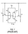
- FIG. 1A 6T CMOS SRAM cell circuit diagram using planar transistors is illustrated in FIG. 1 .
- the SRAM cellconsists of two N-type access devices 102 , two N-type pull-down devices 104 , and two P-type pull-up devices 106 .
- FIG. 3is a graph 300 which illustrates the impact of supply voltage scaling on a typical 6T CMOS SRAM cell using planar transistors.
- the noise margin valuesassume nominal threshold voltage, nominal Vcc, and nominal device sizes.
- Dashed line 310indicates the minimum desired value for SNM, 240 mV.
- the graphshows that as Vcc scales down from 2V to less than 1V, the cell ratio must increase in order to maintain a desirable SNM value.
- For a cell ratio of 1.5 ( 302 )the minimum voltage that can be achieved while maintaining a nominal SNM of 240 mV is slightly less than 2.0V.
- the minimum voltage that can be achieved while maintaining a nominal SNMis less than 1.5V.
- the minimum voltagemay be reduced to less than 1.0V.
- increasing the cell ratiocorresponds to an area penalty in the form of increasing cell size.
- FIG. 1is an illustration of a prior art 6T CMOS SRAM cell circuit diagram using planar transistors.
- FIG. 2is an illustration of a prior art 6T CMOS SRAM cell layout using planar transistors.
- FIG. 3is a graph which illustrates Static Noise Margin as a function of Supply Voltage for a 6T SRAM cell of varying cell ratios.
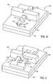
- FIG. 5is a cross-sectional view of a dual fin tri-gate transistor.
- FIG. 7is an illustration of a 6T CMOS SRAM cell layout using single and dual fin tri-gate transistor according to one embodiment of the present invention.
- FIG. 8is a comparison of the gate width of a dual fin tri-gate transistor according to one embodiment of the present invention and a planar transistor.
- FIG. 10is a flowchart which describes the steps in forming a dual fin tri-gate transistor according to one embodiment of the present invention.
- the present inventiontakes advantage of the higher drive current performance of non-planar tri-gate transistors to improve the stability of the 6T CMOS SRAM cell, thus enabling lower supply voltage operation and reduced cell layout sizes.
- Tri-gate transistors in multiple fin configurationscan deliver more drive current for a given layout width than a planar transistor.
- FIG. 5illustrates a cross section of a typical dual fin tri-gate transistor, 500, according to one embodiment of the present invention.
- a dual fin tri-gate transistoris a tri-gate transistor having two semiconductor bodies, or fins, 410 over an insulating substrate 402 , the two fins each having a gate dielectric formed on the top surface and laterally opposite sidewalls, and sharing a single gate electrode formed over and around the gate dielectric.
- Each semiconductor finhas a top surface 412 and laterally opposite sidewalls 414 .
- the semiconductor finsare separated by a distance Ds. Patterning with normal lithographic techniques allows a minimum Ds of approximately 240 nm.
- the gate width of a dual fin tri-gate transistoris equal to the sum of the gate widths for each of the two semiconductor bodies, or [2(Tsi1)+(Wsi1)]+[2(Tsi2)+(Wsi2)]. If the semiconductor bodies are formed in such a way that each semiconductor body has substantially similar dimensions, the gate width of a dual fin tri-gate transistor is effectively twice the gate width of a single fin tri-gate transistor.
- the gate width of a tri-gate transistorcan be further increased by adding additional fins to the tri-gate transistor.
- a tri-gate transistor in a multiple fin configurationcan deliver more drive current for a given layout width than a planar transistor because a tri-gate transistor having the same size as a planar transistor will have a larger gate width.
- the transconductance factor of the dual fin tri-gate transistorwill be greater than that of the single fin tri-gate transistor because the ratio of gate width to gate length for the dual fin device will be greater than that of the single fin device.
- Using a dual fin tri-gate transistor as the pull-down deviceincreases the transconductance factor of the pull-down device, thus increasing the cell ratio of the SRAM cell.
- SNMstatic noise margin
- the use of non-planar tri-gate transistors in the design of an SRAM cellallows the cell ratio to be increased without increasing the physical cell layout size.
- FIG. 7illustrates a 6T CMOS SRAM cell layout using tri-gate transistors according to one embodiment of the present invention.
- the gate of each access deviceis located in region 702 .
- the gate of each pull-down deviceis located in region 704 .
- Each of the pull-down devicesis a dual fin device.
- Each fin of the deviceis indicated by region 708 on either side of sacrificial block 709 .
- Sacrificial block 709is used to form the fins in close proximity to one another. The use of sacrificial block 709 allows the fins to be spaced less than 100 nm from one another, which would not be possible using traditional lithography.
- the gate of each pull-up deviceis located in region 706 .
- the gate regionsare indicated by a region of polysilicon 714 over a region of P-type diffusion 712 or N-type diffusion 710 .
- Metal layers 718provide power (Vcc) and ground (Vss). Metal layers 718 may also connect the gate/source/drain of one planar transistor in the cell to the gate/source/drain of another transistor in the cell, and may connect one SRAM cell to another.
- Contacts 716indicate regions where connections may be made to the metal layers. For a given Vcc, the cell ratio is tailored by sizing the gate width of each access transistor and each pull-down transistor to achieve the maximum SNM value.
- an N-type dual fin tri-gate deviceas the pull-down device and an N-type single fin tri-gate device as the access device allows tri-gate SRAM cell to be designed having a higher cell ratio in the same layout area as a planar SRAM cell.
- G 1 , G 2 , and G 3are formed for each fin of the dual fin tri-gate transistor.
- Each gate formedhas a gate width.
- the gate width of G 1is equal to Z 1 , or the height of the fin.
- the gate width of G 2is equal to Z 2 , or the width of the fin.
- the gate width of G 3is equal to Z 3 , or the height of the fin.
- the total gate width of each finis equal to Z 1 +Z 2 +Z 3 .
- the total gate widthis equal to 2(Z 1 +Z 2 +Z 3 ).
- a tri-gate transistor having N finshas a total gate width equal to N(Z 1 +Z 2 +Z 3 ).
- Z 160 nm
- Z 260 nm
- Z 360 nm
- D s60 nm.
- the gate width of the tri-gate transistor according to this embodimentis 2(60 nm+60 nm+60 nm), or 360 nm.
- Cross-section 820shows a planar transistor formed on a semiconductor substrate 828 .
- the gate width of the planar transistoris equal to the width of transistor gate 822 , or Zp.
- the gate width of planar transistor 820is equal to 180 nm. Because the gate width of the tri-gate transistor is two times that of the planar transistor for the same layout area, it is possible to increase the cell ratio of a 6T CMOS SRAM cell by designing the cell using single and dual fin tri-gate transistors according to one embodiment of the present invention.
- FIG. 9is a graph 900 which illustrates static noise margin (SNM) as a function of VCC for a planar SRAM cell 920 and a tri-gate SRAM cell 910 , where the cells are the same size.
- a tri-gate SRAM cell designallows for lower scaling of VCC before exceeding a lower SNM limit of 240 mV ( 930 ). Because the cell ratio is higher when the SRAM cell is designed using tri-gate transistors according to one embodiment of the present invention, the supply voltage can be scaled lower without reducing the SNM below 240 mV.
- An SRAM cell designed using planar transistorscan be operated at a supply voltage of slightly less than 2.0V without reducing the SNM to less than 240 mV.
- An SRAM cell of the same size, but designed using dual and single fin tri-gate transistors according to one embodiment of the present invention,may be operated at a much lower supply voltage before the SNM limit is met.
- the supply voltagemay be as low as 1.25V before the SNM is reduced to less than 240 mV.
- a silicon or semiconductor filmis formed on an insulating substrate, as described in block 1002 .
- the insulating substrateincludes a lower monocrystalline silicon substrate and a top insulating layer, such as a silicon dioxide film or a silicon nitride film.
- the insulating layeris sometimes referred to as a “buried oxide” layer.
- the semiconductor filmhas a thickness of 60 nm.
- a sacrificial block having a top surface and laterally opposite sidewallsis then formed on the semiconductor film, as described in block 1004 .
- the sacrificial blockis formed by first forming a layer of the sacrificial material and patterning the sacrificial material to form a block using lithography.
- the sacrificial blockmay be comprised of nitride, but is not limited to nitride.
- the width of the sacrificial blockdetermines the spacing of the fins.
- the laterally opposite sidewalls of the sacrificial blockare 60 nm apart.
- the laterally opposite sidewalls of the sacrificial blockare separated by a distance defined by the minimum feature size that may be formed using lithography.
- an insulating layeris formed over and around the sacrificial block and the semiconductor film, as described in block 1006 .
- the insulating layermay be comprised of an oxide or another insulating material.
- the insulating layeris deposited such that the thickness of the layer is approximately equal to the desired semiconductor fin width. In one embodiment of the present invention, the thickness of the insulating layer is between 40 and 80 nm. In another embodiment of the present invention, the thickness of the insulating layer is 60 nm.
- Insulating spacersare then formed on either side of the sacrificial block by performing an anisotropic etch on the insulating layer, as described in block 1008 . After the anisotropic etch, insulating spacers will remain on either side of the sacrificial block. The width of the insulating spacers will be equal to the thickness of the original insulating layer. In one embodiment of the present invention, the insulating spacers are 60 nm wide.
- multiple sacrificial blocksmay be formed, to form additional spacers.
- This methodmay be used to form a tri-gate transistor having more than two fins.
- the number of fins formedwill be equal to the number of insulating spacers.
- an even number of fins (2N)may be formed.
- N sacrificial blocks and 2N insulating spacersare required.
- the sacrificial blockmay be removed by conventional methods, as shown in block 1010 .
- a selective etch processmay be used to remove the sacrificial block, while the insulating spacers remain intact.
- two semiconductor finsare formed by etching the semiconductor film using the insulating spacers as a mask, as shown in block 1012 .
- the semiconductor filmis etched away in areas not covered by the insulating spacers, exposing the insulating substrate.
- Each semiconductor fin formedhas a top surface and a pair of laterally opposite sidewalls.
- Using the insulating spacers as a maskallows the fins to be separated by a distance that is less than the distance that could be achieved using current lithographic technology.
- Current lithographyallows printing of features having minimum sizes near 60 nm and minimum spacing between features of near 240 nm.
- the finscan be formed less than 240 nm apart. In one embodiment of the present invention, the fins are separated by a distance of 60 nm or less.
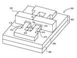
- FIGS. 11A through 11Jillustrate the formation of a dual fin tri-gate transistor according to one embodiment of the present invention.
- the fabrication of a dual fin tri-gate transistorbegins with an insulating substrate 1102 , as shown in FIG. 11A .
- a silicon or semiconductor film 1108is formed on insulating substrate 1102 .
- Insulating substrate 1102may be comprised of a lower monocrystalline silicon substrate 1104 and a top insulating layer 1106 , such as a silicon dioxide or silicon nitride film.
- Insulating layer 1106isolates semiconductor film 1108 from substrate 1104 , and is sometimes referred to as a “buried oxide” layer.
- Semiconductor film 1108may be comprised of silicon or another semiconductor, such as but not limited to germanium (Ge), a silicon-germanium alloy (Si x Ge y ), gallium arsenide (GaAs), InSb, GaP, GaSb, or carbon nanotubes.
- the semiconductor film 1108may be an intrinsic, or undoped, silicon film, or it may be doped to a p-type or n-type conductivity.
- the semiconductor film 1108is formed to a thickness, Tsi, which is approximately equal to the height desired for the subsequently formed semiconductor fins of the tri-gate transistor. In one embodiment of the present invention, the semiconductor film 1108 has a thickness of 60 nm or less.
- FIG. 11Billustrates the formation of a sacrificial block on the top surface of semiconductor film 1108 .
- the sacrificial blockmay be formed by conventional semiconductor manufacturing techniques, including but not limited to depositing a layer of the sacrificial material, 1109 , and subsequently patterning the layer with resist 1111 .
- the sacrificial material that is not covered by resist 1111may be etched to form one or more sacrificial blocks in the desired location(s).
- the sacrificial material 1109is comprised of a nitride.
- the width of the sacrificial block to be formed, Ws,will define the subsequent spacing of the semiconductor fins of the tri-gate transistor.
- Wsis 60 nm or less.
- the use of a sacrificial blockallows the semiconductor fins to be separated by distances of 60 nm or less, which is significantly less than the distance between features that can be achieved by conventional lithography techniques.
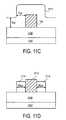
- FIG. 11Cillustrates the formation of an insulating layer 1112 over and around the insulating block 1110 and over the surface of the semiconductor film 1108 .
- the insulating layeris comprised of an oxide.
- the insulating layer 1112is deposited in a manner which allows the layer to have a uniform thickness, Tox. The thickness of the insulating layer will determine the width of the semiconductor fins in a subsequent processing step. In one embodiment of the present invention, the insulating layer has a thickness of 60 nm or less.
- FIG. 11Dillustrates the formation of insulating spacers 1114 .
- Insulating spacers 1114are formed by performing an anisotropic etch on the insulating layer 1112 of FIG. 11C .
- the anisotropic etchis performed in a manner that allows the insulating layer to be entirely removed from the top surface of the sacrificial block 1110 , but leaves insulating spacers 1114 on either side of the sacrificial block.
- the insulating spacers 1114are formed having a width, Wox, which is equal to the thickness of the insulating film of FIG. 11C , Tox. In one embodiment of the present invention, the width, Wox, of each insulating spacer is 60 nm or less.
- FIG. 11Eillustrates the structure formed after the removal of the sacrificial block.
- the sacrificial blockmay be removed by conventional methods, including the use of a selective etch process. For example, a wet etch may be used to remove a sacrificial nitride block, while the oxide spacers will remain unaffected by the etch process.
- a wet etchmay be used to remove a sacrificial nitride block, while the oxide spacers will remain unaffected by the etch process.
- two insulating spacers 1114remain, each spacer having a width equal to Wox.
- the spacersare separated by a distance equal to the width of the sacrificial block, Ws.
- FIG. 11Fillustrates the formation of semiconductor fins 1120 .
- Semiconductor fins 1120are formed by etching semiconductor film 1108 using insulating spacers 1114 as a mask. In one embodiment of the present invention, the etch is a plasma dry etch process. The semiconductor film is etched completely, exposing the surface of insulating substrate 1102 . The semiconductor fins are formed having a width, Wsi, which is equal to the width of the insulating spacers used as a mask. In one embodiment of the present invention, Wsi is 60 nm or less. The semiconductor fins are separated by a distance, Ds, which is equal to the width of the sacrificial block formed previously. In one embodiment of the present invention, Ds is 60 nm or less.
- the insulating spacersmay be removed by conventional techniques, as illustrated in FIG. 11G .
- two semiconductor fins 1120remain on the insulating substrate 1102 .
- the semiconductor fins 1120have a top surface, 1121 , and laterally opposite sidewalls, 1123 .
- the total layout width of the devicewill be equal to Wsi+Ds+Wsi. In one embodiment of the present invention, the total layout width of the device is 180 nm or less.
- FIG. 11Hillustrates the formation of a gate dielectric layer 1122 on the top surface 1121 and on the sidewalls 1123 of each semiconductor fin 1120 .
- the tri-gate transistorcan be designed to be inherently immune from Vt instability by careful control over the geometry of the corners 1125 of the semiconductor fin.
- the corner of the semiconductor finis formed by the intersection of adjacent gates, G 1 , G 2 , and G 3 , (top and side) of the device. Because the corner 1125 of the tri-gate transistor turns on first, it determines the threshold voltage (Vt) of the device. When Vt is set only by dopant implants, there may be fluctuations in the dopants which in turn can cause Vt fluctuations.
- the tri-gate transistorWhen corner rounding is controlled, the tri-gate transistor is not dependent on doping to set the Vt, and so the transistor can be designed to be inherently immune from Vt instability. Corner rounding of the silicon fin arises primarily from the gate dielectric formation process.
- the gate dielectric 1122may be grown or deposited on the surface and sidewalls of the silicon fin.
- the gate dielectric layeris deposited using Atomic Layer Deposition (ALD), which allows corner rounding to be controlled to atomic dimensions.
- ALDAtomic Layer Deposition
- the radius of curvature, R, of each corner of the semiconductor finis less than 10 nm.
- a gate materialis deposited over the top surface and sidewalls of each semiconductor fin and over the insulating substrate, as illustrated in FIG. 11I .
- the gate materialis patterned to form a gate electrode 1124 on the gate dielectric layer.
- source and drain regionsare formed by implanting N-type or P-type dopants into the semiconductor body, as illustrated by arrows 1130 .
- further operationsmay be performed on the tri-gate device, including, but not limited to, formation of tip or source/drain extension regions, halo regions, heavily doped source/drain contact regions, silicon deposited on the source/drain and gate electrode regions, and silicide formation on the source/drain and gate electrode regions.
- each semiconductor fin of the resulting dual fin tri-gate transistorhas a gate width that is equal to 2Tsi+Wsi.
- the gate width for the dual fin tri-gate transistoris equal to the sum of the gate widths for each fin, or 2(2Tsi+Wsi).
- the devicemay be manufactured in an area having a layout width of 2Wsi+Ds.
- the gate width of the dual fin tri-gate transistoris 360 nm or less, and the device is formed in an area having a layout width of 180 nm or less.
- the method set forth abovemay be used to form tri-gate transistors having more than two semiconductor fins.
Landscapes
- Engineering & Computer Science (AREA)
- Microelectronics & Electronic Packaging (AREA)
- Computer Hardware Design (AREA)
- Semiconductor Memories (AREA)
- Metal-Oxide And Bipolar Metal-Oxide Semiconductor Integrated Circuits (AREA)
- Static Random-Access Memory (AREA)
Abstract
Description
- 1. Field of the Invention
- The present invention relates to the field of semiconductor integrated circuit design and manufacturing, and more specifically to a 6T CMOS SRAM cell using tri-gate fully depleted substrate transistors and its methods of fabrication.
- 2. Discussion of Related Art
- As silicon technology continues to scale from one generation to the next, the impact of intrinsic threshold voltage (Vt) variations in minimum geometry size bulk planar transistors reduces the CMOS SRAM cell static noise margin (SNM). This reduction in SNM caused by increasingly smaller transistor geometries is undesirable. SNM is further reduced when Vcc is scaled to a lower voltage.
- Threshold voltage (Vt) variations in planar transistors arise mostly from the statistical fluctuation of the number and/or location of the dopant atoms in the depletion region of the transistors. The Vt variations pose barriers to the scaling of supply voltage, transistor size, and, hence, the minimum six transistor (6T) CMOS SRAM cell size. This limits the total transistor count for conventional 6T SRAM-dominated high performance CMOS ASICs and microprocessors due to die size and cost constraints.
- Currently, the problem of reduced SNM resulting from Vt instability of the SRAM cell transistors is solved at the circuit/layout level by either (a) increasing the minimum supply voltage (Vccmin) needed to operate the cell and keeping the minimum geometry size transistors or (b) increasing the channel length and width of the cell transistors to enable a lower minimum operating voltage at the expense of the minimum cell size. At the device level, in planar devices, Vt mismatch arising from random dopant fluctuations (RDF) can be minimized by box-shaped wells or super-steep retrograde wells at the expense of additional fabrication process complexity.
- A 6T CMOS SRAM cell circuit diagram using planar transistors is illustrated in
FIG. 1 . The SRAM cell consists of two N-type access devices 102, two N-type pull-down devices 104, and two P-type pull-up devices 106. FIG. 2 illustrates a 6T CMOS SRAM cell layout using planar transistors. The gate of each access device is located inregion 202. The gate of each pull-down device is located inregion 204. The gate of each pull-up device is located inregion 206. The gate regions are indicated by a region ofpolysilicon 214 over a region of P-type diffusion 212 or N-type diffusion 210.Metal layers 218 provide power (Vcc) and ground (Vss).Metal layers 218 may also connect the gate/source/drain of one planar transistor in the cell to the gate/source/drain of another transistor in the cell, and may interconnect one cell to another.Contacts 216 indicate regions where connections may be made to the metal layers. For a given Vcc, the cell ratio is tailored by sizing each access transistor width and each pull-down transistor width to achieve the maximum SNM value.FIG. 3 is agraph 300 which illustrates the impact of supply voltage scaling on a typical 6T CMOS SRAM cell using planar transistors. The noise margin values assume nominal threshold voltage, nominal Vcc, and nominal device sizes. Dashedline 310 indicates the minimum desired value for SNM, 240 mV. The graph shows that as Vcc scales down from 2V to less than 1V, the cell ratio must increase in order to maintain a desirable SNM value. For a cell ratio of 1.5 (302), the minimum voltage that can be achieved while maintaining a nominal SNM of 240 mV is slightly less than 2.0V. When the cell ratio is increased to 2.0 (304), the minimum voltage that can be achieved while maintaining a nominal SNM is less than 1.5V. If the cell ratio is increased to 3.5 (306), the minimum voltage may be reduced to less than 1.0V. However, increasing the cell ratio corresponds to an area penalty in the form of increasing cell size.FIG. 1 is an illustration of a prior art 6T CMOS SRAM cell circuit diagram using planar transistors.FIG. 2 is an illustration of a prior art 6T CMOS SRAM cell layout using planar transistors.FIG. 3 is a graph which illustrates Static Noise Margin as a function of Supply Voltage for a 6T SRAM cell of varying cell ratios.FIG. 4 is a cross-sectional view of a single-fin tri-gate transistor.FIG. 5 is a cross-sectional view of a dual fin tri-gate transistor.FIG. 6 is an illustration of a 6T CMOS SRAM cell circuit diagram with tri-gate transistors according to one embodiment of the present invention.FIG. 7 is an illustration of a 6T CMOS SRAM cell layout using single and dual fin tri-gate transistor according to one embodiment of the present invention.FIG. 8 is a comparison of the gate width of a dual fin tri-gate transistor according to one embodiment of the present invention and a planar transistor.FIG. 9 is a graph which compares SNM as a function of supply voltage for a tri-gate SRAM according to one embodiment of the present invention and for a planar SRAM, where both SRAM cells have the same layout area.FIG. 10 is a flowchart which describes the steps in forming a dual fin tri-gate transistor according to one embodiment of the present invention.FIGS. 11A-11J illustrate the formation of a dual fin tri-gate transistor according to one embodiment of the present invention.- The present invention is a 6T CMOS SRAM cell using non-planar tri-gate transistors, and its method of fabrication. In the following description, numerous specific details are set forth in order to provide a thorough understanding of the present invention. In other instances, well-known semiconductor process and manufacturing techniques have not been described in particular detail in order to not unnecessarily obscure the present invention.
- The present invention takes advantage of the higher drive current performance of non-planar tri-gate transistors to improve the stability of the 6T CMOS SRAM cell, thus enabling lower supply voltage operation and reduced cell layout sizes. Tri-gate transistors in multiple fin configurations can deliver more drive current for a given layout width than a planar transistor.
FIG. 4 illustrates a cross section of a typical single fin tri-gatetransistor 400. A single fin tri-gate transistor is a tri-gate transistor having asingle semiconductor body 410. The semiconductor body will also be referred to as a “semiconductor fin.” The semiconductor body is formed on aninsulating substrate 402. The insulating substrate is comprised of a buried oxide or otherinsulating layer 406 over a silicon orother semiconductor substrate 404. A gate dielectric416 is formed over the top and on the sides of thesemiconductor fin 410. Agate electrode 420 is formed over the top and on the sides of the gate dielectric. The gate electrode has a gate length GL. The source, S, and drain, D, regions are formed in the semiconductor fin on either side of the gate electrode.- The semiconductor fin has a
top surface 412 and laterallyopposite sidewalls 414. The semiconductor fin has a height or thickness equal to Tsi. The semiconductor fin has a width equal to Wsi. The gate width of a single fin tri-gate transistor is equal to the sum of the gate widths of each of the three gates formed on the semiconductor body, or, Tsi+Wsi+Tsi. FIG. 5 illustrates a cross section of a typical dual fin tri-gate transistor, 500, according to one embodiment of the present invention. A dual fin tri-gate transistor is a tri-gate transistor having two semiconductor bodies, or fins,410 over aninsulating substrate 402, the two fins each having a gate dielectric formed on the top surface and laterally opposite sidewalls, and sharing a single gate electrode formed over and around the gate dielectric. Each semiconductor fin has atop surface 412 and laterallyopposite sidewalls 414. The semiconductor fins are separated by a distance Ds. Patterning with normal lithographic techniques allows a minimum Ds of approximately 240 nm. The gate width of a dual fin tri-gate transistor is equal to the sum of the gate widths for each of the two semiconductor bodies, or [2(Tsi1)+(Wsi1)]+[2(Tsi2)+(Wsi2)]. If the semiconductor bodies are formed in such a way that each semiconductor body has substantially similar dimensions, the gate width of a dual fin tri-gate transistor is effectively twice the gate width of a single fin tri-gate transistor. The gate width of a tri-gate transistor can be further increased by adding additional fins to the tri-gate transistor. A tri-gate transistor in a multiple fin configuration can deliver more drive current for a given layout width than a planar transistor because a tri-gate transistor having the same size as a planar transistor will have a larger gate width.FIG. 6 illustrates a 6T CMOS SRAM cell circuit diagram using tri-gate transistors according to one embodiment of the present invention. The SRAM cell consists of two N-type access devices,602, two N-type pull-down devices,604, and two P-type pull-up devices,606. Each of the N-type access devices 602 is a single fin tri-gate transistor. Each of the P-type pull-updevices 606 is a single fin tri-gate transistor. Each of the N-type pull-downdevices 604 is a dual fin tri-gate transistor. Using a dual fin tri-gate transistor as the pull-down device allows a circuit designer to achieve a higher cell ratio for the SRAM cell. The dual fin tri-gate transistor will deliver more current than the single fin tri-gate transistors, thus increasing the cell ratio without increasing the cell layout size.- The cell ratio of an SRAM cell is defined as the ratio of the transconductance factor of the pull-down N-type transistor to the transconductance factor of the access N-type transistor. The transconductance factor of a transistor is equal to the ratio of gate width to gate length times the mobility and gate capacitance. Where mobility and gate capacitance are constant across the access and pull-down transistors, the transconductance factor becomes the ratio of the transistor gate width to the transistor gate length. The transconductance factor of the dual fin tri-gate transistor will be greater than that of the planar transistor, because the transistor gate width of the dual fin tri-gate transistor is greater that of the planar transistor, within the same layout area. Furthermore, the transconductance factor of the dual fin tri-gate transistor will be greater than that of the single fin tri-gate transistor because the ratio of gate width to gate length for the dual fin device will be greater than that of the single fin device. Using a dual fin tri-gate transistor as the pull-down device increases the transconductance factor of the pull-down device, thus increasing the cell ratio of the SRAM cell. As described above, higher, and thus more desirable static noise margin (SNM) levels can be achieved by increasing the cell ratio. The use of non-planar tri-gate transistors in the design of an SRAM cell allows the cell ratio to be increased without increasing the physical cell layout size. Table 1, below, is a comparison of cell ratios for an SRAM cell using planar transistors and an SRAM cell using tri-gate transistors, where each of the SRAM cells has the same layout area.
TABLE 1 Transistor Transconductance Planar SRAM Cell* Pull Down 1.6 Cell Ratio = 1.5 Access 1.1 Pull Up 1.3 Tri-gate SRAM Cell* Pull Down 6.0 Cell Ratio = 2.15 Access 2.8 Pull Up 3.0
*Note:
Cell layout areas are the same for each cell FIG. 7 illustrates a 6T CMOS SRAM cell layout using tri-gate transistors according to one embodiment of the present invention. The gate of each access device is located inregion 702. The gate of each pull-down device is located inregion 704. Each of the pull-down devices is a dual fin device. Each fin of the device is indicated byregion 708 on either side ofsacrificial block 709.Sacrificial block 709 is used to form the fins in close proximity to one another. The use ofsacrificial block 709 allows the fins to be spaced less than 100 nm from one another, which would not be possible using traditional lithography. The gate of each pull-up device is located inregion 706. The gate regions are indicated by a region ofpolysilicon 714 over a region of P-type diffusion 712 or N-type diffusion 710. Metal layers718 provide power (Vcc) and ground (Vss). Metal layers718 may also connect the gate/source/drain of one planar transistor in the cell to the gate/source/drain of another transistor in the cell, and may connect one SRAM cell to another.Contacts 716 indicate regions where connections may be made to the metal layers. For a given Vcc, the cell ratio is tailored by sizing the gate width of each access transistor and each pull-down transistor to achieve the maximum SNM value. As described above, using an N-type dual fin tri-gate device as the pull-down device and an N-type single fin tri-gate device as the access device allows tri-gate SRAM cell to be designed having a higher cell ratio in the same layout area as a planar SRAM cell.FIG. 8 is a comparison of the gate width of a dual fin tri-gate transistor according to one embodiment of the present invention to the gate width of a planar transistor in the same layout area.Cross-section 800 shows a dual fin tri-gate transistor formed on an insulatingsubstrate 808. The fins of the tri-gate transistor are formed bysemiconductor bodies 802. The fins are separated by a distance, Ds, which is determined by the width of the sacrificial block described above. The distance, Ds, may be defined by the minimum lithography feature size that may be patterned. Agate dielectric 804 covers each fin of the tri-gate transistor in the gate region.Gate electrode 806 is formed over and around each semiconductor fin and gate dielectric layer. Three gates, G1, G2, and G3 are formed for each fin of the dual fin tri-gate transistor. Each gate formed has a gate width. The gate width of G1 is equal to Z1, or the height of the fin. The gate width of G2 is equal to Z2, or the width of the fin. The gate width of G3 is equal to Z3, or the height of the fin. The total gate width of each fin is equal to Z1+Z2+Z3. For a dual fin tri-gate transistor, the total gate width is equal to 2(Z1+Z2+Z3). A tri-gate transistor having N fins has a total gate width equal to N(Z1+Z2+Z3). In one embodiment of the present invention, Z1=60 nm, Z2=60 nm, Z3=60 nm, and Ds=60 nm. The gate width of the tri-gate transistor according to this embodiment is 2(60 nm+60 nm+60 nm), or 360 nm. The total layout width used is equal to Z3+Ds+Z3, or (60 nm+60 nm+60 nm)=180 nm.Cross-section 820 shows a planar transistor formed on asemiconductor substrate 828. The gate width of the planar transistor is equal to the width oftransistor gate 822, or Zp. For a layout width of 180 nm, the gate width ofplanar transistor 820 is equal to 180 nm. Because the gate width of the tri-gate transistor is two times that of the planar transistor for the same layout area, it is possible to increase the cell ratio of a 6T CMOS SRAM cell by designing the cell using single and dual fin tri-gate transistors according to one embodiment of the present invention.FIG. 9 is agraph 900 which illustrates static noise margin (SNM) as a function of VCC for aplanar SRAM cell 920 and atri-gate SRAM cell 910, where the cells are the same size. A tri-gate SRAM cell design allows for lower scaling of VCC before exceeding a lower SNM limit of 240 mV (930). Because the cell ratio is higher when the SRAM cell is designed using tri-gate transistors according to one embodiment of the present invention, the supply voltage can be scaled lower without reducing the SNM below 240 mV. An SRAM cell designed using planar transistors can be operated at a supply voltage of slightly less than 2.0V without reducing the SNM to less than 240 mV. An SRAM cell of the same size, but designed using dual and single fin tri-gate transistors according to one embodiment of the present invention, may be operated at a much lower supply voltage before the SNM limit is met. The supply voltage may be as low as 1.25V before the SNM is reduced to less than 240 mV.FIG. 10 is a flow diagram,1000, showing a process in accordance with the present invention, illustrating a general method for forming a multiple fin tri-gate transistor having a reduced layout width. Each block in flow diagram1000 is illustrated and described in further detail below, in conjunction withFIGS. 11A-11J .- A silicon or semiconductor film is formed on an insulating substrate, as described in
block 1002. The insulating substrate includes a lower monocrystalline silicon substrate and a top insulating layer, such as a silicon dioxide film or a silicon nitride film. The insulating layer is sometimes referred to as a “buried oxide” layer. In one embodiment of the present invention, the semiconductor film has a thickness of 60 nm. - A sacrificial block having a top surface and laterally opposite sidewalls is then formed on the semiconductor film, as described in
block 1004. In one embodiment of the present invention, the sacrificial block is formed by first forming a layer of the sacrificial material and patterning the sacrificial material to form a block using lithography. The sacrificial block may be comprised of nitride, but is not limited to nitride. The width of the sacrificial block determines the spacing of the fins. In one embodiment of the present invention, the laterally opposite sidewalls of the sacrificial block are 60 nm apart. In another embodiment of the present invention, the laterally opposite sidewalls of the sacrificial block are separated by a distance defined by the minimum feature size that may be formed using lithography. - After forming the sacrificial block, an insulating layer is formed over and around the sacrificial block and the semiconductor film, as described in
block 1006. The insulating layer may be comprised of an oxide or another insulating material. The insulating layer is deposited such that the thickness of the layer is approximately equal to the desired semiconductor fin width. In one embodiment of the present invention, the thickness of the insulating layer is between 40 and 80 nm. In another embodiment of the present invention, the thickness of the insulating layer is 60 nm. - Insulating spacers are then formed on either side of the sacrificial block by performing an anisotropic etch on the insulating layer, as described in
block 1008. After the anisotropic etch, insulating spacers will remain on either side of the sacrificial block. The width of the insulating spacers will be equal to the thickness of the original insulating layer. In one embodiment of the present invention, the insulating spacers are 60 nm wide. - In another embodiment of the present invention, multiple sacrificial blocks may be formed, to form additional spacers. This method may be used to form a tri-gate transistor having more than two fins. The number of fins formed will be equal to the number of insulating spacers. In one embodiment of the present invention, an even number of fins (2N) may be formed. To form a tri-gate transistor having 2N fins, N sacrificial blocks and 2N insulating spacers are required.
- After the insulating spacers are formed, the sacrificial block may be removed by conventional methods, as shown in
block 1010. For example, a selective etch process may be used to remove the sacrificial block, while the insulating spacers remain intact. - Next, two semiconductor fins are formed by etching the semiconductor film using the insulating spacers as a mask, as shown in
block 1012. The semiconductor film is etched away in areas not covered by the insulating spacers, exposing the insulating substrate. Each semiconductor fin formed has a top surface and a pair of laterally opposite sidewalls. Using the insulating spacers as a mask allows the fins to be separated by a distance that is less than the distance that could be achieved using current lithographic technology. Current lithography allows printing of features having minimum sizes near 60 nm and minimum spacing between features of near 240 nm. Using an embodiment of a method according to the present invention, the fins can be formed less than 240 nm apart. In one embodiment of the present invention, the fins are separated by a distance of 60 nm or less. FIGS. 11A through 11J illustrate the formation of a dual fin tri-gate transistor according to one embodiment of the present invention. The fabrication of a dual fin tri-gate transistor begins with an insulatingsubstrate 1102, as shown inFIG. 11A . A silicon orsemiconductor film 1108 is formed on insulatingsubstrate 1102. Insulatingsubstrate 1102 may be comprised of a lower monocrystalline silicon substrate1104 and a top insulatinglayer 1106, such as a silicon dioxide or silicon nitride film. Insulatinglayer 1106 isolatessemiconductor film 1108 from substrate1104, and is sometimes referred to as a “buried oxide” layer.Semiconductor film 1108 may be comprised of silicon or another semiconductor, such as but not limited to germanium (Ge), a silicon-germanium alloy (SixGey), gallium arsenide (GaAs), InSb, GaP, GaSb, or carbon nanotubes. Thesemiconductor film 1108 may be an intrinsic, or undoped, silicon film, or it may be doped to a p-type or n-type conductivity. Thesemiconductor film 1108 is formed to a thickness, Tsi, which is approximately equal to the height desired for the subsequently formed semiconductor fins of the tri-gate transistor. In one embodiment of the present invention, thesemiconductor film 1108 has a thickness of 60 nm or less.FIG. 11B illustrates the formation of a sacrificial block on the top surface ofsemiconductor film 1108. The sacrificial block may be formed by conventional semiconductor manufacturing techniques, including but not limited to depositing a layer of the sacrificial material,1109, and subsequently patterning the layer with resist1111. The sacrificial material that is not covered by resist1111 may be etched to form one or more sacrificial blocks in the desired location(s). In one embodiment of the present invention, thesacrificial material 1109 is comprised of a nitride. The width of the sacrificial block to be formed, Ws, will define the subsequent spacing of the semiconductor fins of the tri-gate transistor. In one embodiment of the present invention, Ws is 60 nm or less. The use of a sacrificial block allows the semiconductor fins to be separated by distances of 60 nm or less, which is significantly less than the distance between features that can be achieved by conventional lithography techniques.FIG. 11C illustrates the formation of an insulatinglayer 1112 over and around the insulatingblock 1110 and over the surface of thesemiconductor film 1108. In one embodiment of the present invention, the insulating layer is comprised of an oxide. The insulatinglayer 1112 is deposited in a manner which allows the layer to have a uniform thickness, Tox. The thickness of the insulating layer will determine the width of the semiconductor fins in a subsequent processing step. In one embodiment of the present invention, the insulating layer has a thickness of 60 nm or less.FIG. 11D illustrates the formation of insulatingspacers 1114. Insulatingspacers 1114 are formed by performing an anisotropic etch on the insulatinglayer 1112 ofFIG. 11C . The anisotropic etch is performed in a manner that allows the insulating layer to be entirely removed from the top surface of thesacrificial block 1110, but leaves insulatingspacers 1114 on either side of the sacrificial block. The insulatingspacers 1114 are formed having a width, Wox, which is equal to the thickness of the insulating film ofFIG. 11C , Tox. In one embodiment of the present invention, the width, Wox, of each insulating spacer is 60 nm or less.FIG. 11E illustrates the structure formed after the removal of the sacrificial block. The sacrificial block may be removed by conventional methods, including the use of a selective etch process. For example, a wet etch may be used to remove a sacrificial nitride block, while the oxide spacers will remain unaffected by the etch process. After the sacrificial block is removed, two insulatingspacers 1114 remain, each spacer having a width equal to Wox. The spacers are separated by a distance equal to the width of the sacrificial block, Ws.FIG. 11F illustrates the formation ofsemiconductor fins 1120.Semiconductor fins 1120 are formed by etchingsemiconductor film 1108 using insulatingspacers 1114 as a mask. In one embodiment of the present invention, the etch is a plasma dry etch process. The semiconductor film is etched completely, exposing the surface of insulatingsubstrate 1102. The semiconductor fins are formed having a width, Wsi, which is equal to the width of the insulating spacers used as a mask. In one embodiment of the present invention, Wsi is 60 nm or less. The semiconductor fins are separated by a distance, Ds, which is equal to the width of the sacrificial block formed previously. In one embodiment of the present invention, Ds is 60 nm or less.- After the
semiconductor fins 1120 are formed, the insulating spacers may be removed by conventional techniques, as illustrated inFIG. 11G . At this point, twosemiconductor fins 1120 remain on the insulatingsubstrate 1102. Thesemiconductor fins 1120 have a top surface,1121, and laterally opposite sidewalls,1123. The total layout width of the device will be equal to Wsi+Ds+Wsi. In one embodiment of the present invention, the total layout width of the device is 180 nm or less. FIG. 11H illustrates the formation of agate dielectric layer 1122 on thetop surface 1121 and on thesidewalls 1123 of eachsemiconductor fin 1120. The tri-gate transistor can be designed to be inherently immune from Vt instability by careful control over the geometry of thecorners 1125 of the semiconductor fin. The corner of the semiconductor fin is formed by the intersection of adjacent gates, G1, G2, and G3, (top and side) of the device. Because thecorner 1125 of the tri-gate transistor turns on first, it determines the threshold voltage (Vt) of the device. When Vt is set only by dopant implants, there may be fluctuations in the dopants which in turn can cause Vt fluctuations. When corner rounding is controlled, the tri-gate transistor is not dependent on doping to set the Vt, and so the transistor can be designed to be inherently immune from Vt instability. Corner rounding of the silicon fin arises primarily from the gate dielectric formation process. Thegate dielectric 1122 may be grown or deposited on the surface and sidewalls of the silicon fin. In one embodiment of the present invention, the gate dielectric layer is deposited using Atomic Layer Deposition (ALD), which allows corner rounding to be controlled to atomic dimensions. In one embodiment of the present invention, the radius of curvature, R, of each corner of the semiconductor fin is less than 10 nm.- Next, a gate material is deposited over the top surface and sidewalls of each semiconductor fin and over the insulating substrate, as illustrated in
FIG. 11I . The gate material is patterned to form agate electrode 1124 on the gate dielectric layer. - After the gate electrode is formed, a pair of source/drain regions is formed in each semiconductor fin on opposite sides of the gate electrode, as illustrated in
FIG. 11J . In one embodiment of the present invention, source and drain regions are formed by implanting N-type or P-type dopants into the semiconductor body, as illustrated byarrows 1130. In embodiments of the present invention, further operations may be performed on the tri-gate device, including, but not limited to, formation of tip or source/drain extension regions, halo regions, heavily doped source/drain contact regions, silicon deposited on the source/drain and gate electrode regions, and silicide formation on the source/drain and gate electrode regions. - As illustrated in
FIG. 11J , each semiconductor fin of the resulting dual fin tri-gate transistor has a gate width that is equal to 2Tsi+Wsi. The gate width for the dual fin tri-gate transistor is equal to the sum of the gate widths for each fin, or 2(2Tsi+Wsi). The device may be manufactured in an area having a layout width of 2Wsi+Ds. In one embodiment of the present invention, the gate width of the dual fin tri-gate transistor is 360 nm or less, and the device is formed in an area having a layout width of 180 nm or less. - In other embodiments of the present invention, the method set forth above may be used to form tri-gate transistors having more than two semiconductor fins.
Claims (33)
1. A circuit comprising:
at least one access device, the at least one access device comprised of a non-planar transistor having a single fin;
at least one pull-up device, the at least one pull-up device comprised of a non-planar transistor having a single fin; and
at least one pull-down device, the at least one pull-down device comprised of a non-planar transistor having multiple fins.
2. The circuit ofclaim 1 , wherein the at least one pull-down device is comprised of a non-planar tri-gate transistor having two fins.
3. The circuit ofclaim 2 , wherein the two fins of the non-planar tri-gate transistor are located less than 60 nm from each other.
4. A CMOS SRAM cell comprising:
two access devices, each access device comprised of a tri-gate transistor having a single fin;
two pull-up devices, each pull-up device comprised of a tri-gate transistor having a single fin;
two pull-down devices, each pull-down device comprised of a tri-gate transistor having multiple fins; and
wherein the CMOS SRAM cell has a cell ratio, a static noise margin (SNM), and a supply voltage.
5. The CMOS SRAM cell ofclaim 4 , wherein each pull-down device is comprised of a tri-gate transistor having two fins, each fin having a height and a width.
6. The CMOS SRAM cell ofclaim 5 , wherein the fins are located less than 60 nm from each other.
7. The CMOS SRAM cell ofclaim 5 , wherein the height of each fin is 60 nm.
8. The CMOS SRAM cell ofclaim 5 , wherein the width of each fin is 60 nm.
9. The CMOS SRAM cell ofclaim 4 , wherein each tri-gate transistor contains at least one corner, each corner having a radius of curvature of less than 10 nm.
10. The CMOS SRAM cell ofclaim 4 , wherein the cell ratio is greater than 2.0.
11. The CMOS SRAM cell ofclaim 4 , wherein the static noise margin (SNM) is greater than 240 mV.
12. The CMOS SRAM cell ofclaim 11 , wherein the supply voltage is less than 1.5 V.
13. A CMOS SRAM cell comprising:
two N-type access devices, each N-type access device comprised of a tri-gate transistor having a single fin;
two P-type pull-up devices, each P-type pull-up device comprised of a tri-gate transistor having a single fin;
two N-type pull-down devices, each N-type pull-down device comprised of a tri-gate transistor having multiple fins.
14. The CMOS SRAM cell ofclaim 13 , wherein each N-type pull-down device is comprised of a tri-gate transistor having two fins, each fin having a height and a width.
15. The CMOS SRAM cell ofclaim 14 , wherein the fins are located less than 60 nm from each other.
16. A method of forming a six transistor (6T) CMOS SRAM cell, comprising:
forming two N-type access devices, each N-type access device comprised of a tri-gate transistor having a single fin;
forming two P-type pull-up devices, each P-type pull-up device comprised of a tri-gate transistor having a single fin;
forming two N-type pull-down devices, each N-type pull-down device comprised of a tri-gate transistor having at least two fins.
17. A method of forming a semiconductor device, comprising:
forming a silicon film on a substrate;
forming a sacrificial block on the silicon film, the sacrificial block having laterally opposite sidewalls;
depositing an insulating layer over the sacrificial block and the silicon film;
forming an insulating spacer on each of the laterally opposite sidewalls of the nitride block by performing an anisotropic etch on the insulating layer;
removing the sacrificial block;
forming two silicon fins by etching through the silicon film to the substrate using the insulating spacers as a mask, wherein each silicon fin has a top surface and a pair of laterally opposite sidewalls; and
removing the insulating spacers to expose the top surface of each silicon fin.
18. The method ofclaim 17 , wherein the substrate is an insulating substrate.
19. The method ofclaim 17 , wherein the insulating layer is comprised of an oxide layer.
20. The method ofclaim 17 , wherein the thickness of the silicon film is 60 nm.
21. The method ofclaim 17 , wherein the laterally opposite sidewalls of the sacrificial block are 60 nm apart.
22. The method ofclaim 17 , wherein the sacrificial block is defined by lithography.
23. The method ofclaim 18 , wherein the sacrificial block is comprised of nitride.
24. The method ofclaim 17 , wherein the thickness of the insulating layer is between 40 and 80 nm.
25. The method ofclaim 17 , wherein the thickness of the insulating layer is 60 nm.
26. The method ofclaim 17 , wherein the two silicon fins are separated by a distance of 60 nm or less.
27. The method ofclaim 17 , further comprising forming a gate dielectric layer on the top surface and on the sidewalls of each silicon fin.
28. The method ofclaim 27 , wherein the gate dielectric layer is formed by atomic layer deposition (ALD).
29. The method ofclaim 28 , wherein each silicon fin has at least one corner having a radius of curvature, the radius of curvature being defined by the atomic layer deposition of the gate dielectric layer.
30. The method ofclaim 29 , wherein the radius of curvature is less than 10 nm.
31. The method ofclaim 27 , further comprising depositing a gate material over the top surface and sidewalls of each silicon fin and over the insulating substrate.
32. The method ofclaim 31 , further comprising patterning the gate material to form a gate electrode on the gate dielectric layer.
33. The method ofclaim 32 , further comprising forming a pair of source/drain regions in each silicon fin on opposite sides of the gate electrode.
Priority Applications (10)
| Application Number | Priority Date | Filing Date | Title |
|---|---|---|---|
| US10/679,124US6970373B2 (en) | 2003-10-02 | 2003-10-02 | Method and apparatus for improving stability of a 6T CMOS SRAM cell |
| TW093114516ATWI267858B (en) | 2003-10-02 | 2004-05-21 | A method and apparatus for improving stability of a 6T CMOS SRAM cell |
| JP2006534164AJP2007509490A (en) | 2003-10-02 | 2004-09-29 | 6-transistor FINFET type CMOS static RAM cell with increased cell ratio |
| DE112004001864.1TDE112004001864B4 (en) | 2003-10-02 | 2004-09-29 | Method and apparatus for improving the stability of a 6-transistor CMOS SRAM cell |
| KR1020067007629AKR100915398B1 (en) | 2003-10-02 | 2004-09-29 | 6t finfet cmos sram cell with an increased cell ratio |
| KR1020087025417AKR20080106978A (en) | 2003-10-02 | 2004-09-29 | Circuit, CMOS SRM Cell, 6T CMOS SRM Cell Formation Method, Semiconductor Device Formation Method |
| CNB2004800356519ACN100477168C (en) | 2003-10-02 | 2004-09-29 | Method and device for improving stability of 6T CMOS SRAM cell |
| PCT/US2004/032442WO2005034212A2 (en) | 2003-10-02 | 2004-09-29 | 6t finfet cmos sram cell with an increased cell ratio |
| US11/165,724US7138305B2 (en) | 2003-10-02 | 2005-06-24 | Method and apparatus for improving stability of a 6T CMOS SRAM cell |
| US11/508,009US7445980B2 (en) | 2003-10-02 | 2006-08-21 | Method and apparatus for improving stability of a 6T CMOS SRAM cell |
Applications Claiming Priority (1)
| Application Number | Priority Date | Filing Date | Title |
|---|---|---|---|
| US10/679,124US6970373B2 (en) | 2003-10-02 | 2003-10-02 | Method and apparatus for improving stability of a 6T CMOS SRAM cell |
Related Child Applications (1)
| Application Number | Title | Priority Date | Filing Date |
|---|---|---|---|
| US11/165,724DivisionUS7138305B2 (en) | 2003-10-02 | 2005-06-24 | Method and apparatus for improving stability of a 6T CMOS SRAM cell |
Publications (2)
| Publication Number | Publication Date |
|---|---|
| US20050073060A1true US20050073060A1 (en) | 2005-04-07 |
| US6970373B2 US6970373B2 (en) | 2005-11-29 |
Family
ID=34394102
Family Applications (3)
| Application Number | Title | Priority Date | Filing Date |
|---|---|---|---|
| US10/679,124Expired - LifetimeUS6970373B2 (en) | 2003-10-02 | 2003-10-02 | Method and apparatus for improving stability of a 6T CMOS SRAM cell |
| US11/165,724Expired - Fee RelatedUS7138305B2 (en) | 2003-10-02 | 2005-06-24 | Method and apparatus for improving stability of a 6T CMOS SRAM cell |
| US11/508,009Expired - LifetimeUS7445980B2 (en) | 2003-10-02 | 2006-08-21 | Method and apparatus for improving stability of a 6T CMOS SRAM cell |
Family Applications After (2)
| Application Number | Title | Priority Date | Filing Date |
|---|---|---|---|
| US11/165,724Expired - Fee RelatedUS7138305B2 (en) | 2003-10-02 | 2005-06-24 | Method and apparatus for improving stability of a 6T CMOS SRAM cell |
| US11/508,009Expired - LifetimeUS7445980B2 (en) | 2003-10-02 | 2006-08-21 | Method and apparatus for improving stability of a 6T CMOS SRAM cell |
Country Status (7)
| Country | Link |
|---|---|
| US (3) | US6970373B2 (en) |
| JP (1) | JP2007509490A (en) |
| KR (2) | KR20080106978A (en) |
| CN (1) | CN100477168C (en) |
| DE (1) | DE112004001864B4 (en) |
| TW (1) | TWI267858B (en) |
| WO (1) | WO2005034212A2 (en) |
Cited By (263)
| Publication number | Priority date | Publication date | Assignee | Title |
|---|---|---|---|---|
| US20060237857A1 (en)* | 2005-01-14 | 2006-10-26 | Nantero, Inc. | Hybrid carbon nanotube FET(CNFET)-FET static RAM (SRAM) and method of making same |
| US20060268626A1 (en)* | 2005-05-25 | 2006-11-30 | Fatih Hamzaoglu | Memory with dynamically adjustable supply |
| US20070058419A1 (en)* | 2005-09-13 | 2007-03-15 | Intel Corporation | Memory cell having p-type pass device |
| US20070108528A1 (en)* | 2005-11-15 | 2007-05-17 | International Business Machines Corporation | Sram cell |
| US20070152266A1 (en)* | 2005-12-29 | 2007-07-05 | Intel Corporation | Method and structure for reducing the external resistance of a three-dimensional transistor through use of epitaxial layers |
| US20070202659A1 (en)* | 2004-10-29 | 2007-08-30 | International Business Machines Corporation | FinFET Body Contact Structure |
| US20080067613A1 (en)* | 2006-09-15 | 2008-03-20 | Anderson Brent A | Field effect transistor with raised source/drain fin straps |
| US20080191282A1 (en)* | 2007-02-12 | 2008-08-14 | Infineon Technologies Agst | Mugfet array layout |
| US7432557B1 (en) | 2003-07-08 | 2008-10-07 | Advanced Micro Devices, Inc. | FinFET device with multiple channels |
| US7498225B1 (en) | 2003-12-04 | 2009-03-03 | Advanced Micro Devices, Inc. | Systems and methods for forming multiple fin structures using metal-induced-crystallization |
| US20090086528A1 (en)* | 2007-09-27 | 2009-04-02 | Micron Technology, Inc. | Back gated sram cell |
| US20090090976A1 (en)* | 2005-09-28 | 2009-04-09 | Intel Corporation | Process for integrating planar and non-planar cmos transistors on a bulk substrate and article made thereby |
| US20090149531A1 (en)* | 2007-12-11 | 2009-06-11 | Apoteknos Para La Piel, S.L. | Chemical composition derived from p-hydroxyphenyl propionic acid for the treatment of psoriasis |
| US20090149012A1 (en)* | 2004-09-30 | 2009-06-11 | Brask Justin K | Method of forming a nonplanar transistor with sidewall spacers |
| US7679134B1 (en)* | 2002-11-26 | 2010-03-16 | Globalfoundries | FinFET device with multiple fin structures |
| US7736956B2 (en) | 2005-08-17 | 2010-06-15 | Intel Corporation | Lateral undercut of metal gate in SOI device |
| US7781771B2 (en) | 2004-03-31 | 2010-08-24 | Intel Corporation | Bulk non-planar transistor having strained enhanced mobility and methods of fabrication |
| US7820513B2 (en) | 2003-06-27 | 2010-10-26 | Intel Corporation | Nonplanar semiconductor device with partially or fully wrapped around gate electrode and methods of fabrication |
| US7879675B2 (en) | 2005-03-14 | 2011-02-01 | Intel Corporation | Field effect transistor with metal source/drain regions |
| US20110037497A1 (en)* | 2009-04-14 | 2011-02-17 | Or-Ment Llc | Method for Fabrication of a Semiconductor Device and Structure |
| US7898041B2 (en) | 2005-06-30 | 2011-03-01 | Intel Corporation | Block contact architectures for nanoscale channel transistors |
| US7902014B2 (en) | 2005-09-28 | 2011-03-08 | Intel Corporation | CMOS devices with a single work function gate electrode and method of fabrication |
| US7960794B2 (en) | 2004-08-10 | 2011-06-14 | Intel Corporation | Non-planar pMOS structure with a strained channel region and an integrated strained CMOS flow |
| US7989280B2 (en) | 2005-11-30 | 2011-08-02 | Intel Corporation | Dielectric interface for group III-V semiconductor device |
| US20110199116A1 (en)* | 2010-02-16 | 2011-08-18 | NuPGA Corporation | Method for fabrication of a semiconductor device and structure |
| CN102197467A (en)* | 2008-11-06 | 2011-09-21 | 高通股份有限公司 | A method of fabricating a fin field effect transistor (FINFET) device |
| US8067818B2 (en) | 2004-10-25 | 2011-11-29 | Intel Corporation | Nonplanar device with thinned lower body portion and method of fabrication |
| US8071983B2 (en) | 2005-06-21 | 2011-12-06 | Intel Corporation | Semiconductor device structures and methods of forming semiconductor structures |
| US8084818B2 (en) | 2004-06-30 | 2011-12-27 | Intel Corporation | High mobility tri-gate devices and methods of fabrication |
| US8183646B2 (en) | 2005-02-23 | 2012-05-22 | Intel Corporation | Field effect transistor with narrow bandgap source and drain regions and method of fabrication |
| US8268709B2 (en) | 2004-09-29 | 2012-09-18 | Intel Corporation | Independently accessed double-gate and tri-gate transistors in same process flow |
| US20120319212A1 (en)* | 2009-12-07 | 2012-12-20 | Taiwan Semiconductor Manufacturing Company, Ltd. | SRAM Structure with FinFETs Having Multiple Fins |
| US8362482B2 (en) | 2009-04-14 | 2013-01-29 | Monolithic 3D Inc. | Semiconductor device and structure |
| US8362566B2 (en) | 2008-06-23 | 2013-01-29 | Intel Corporation | Stress in trigate devices using complimentary gate fill materials |
| US8362800B2 (en) | 2010-10-13 | 2013-01-29 | Monolithic 3D Inc. | 3D semiconductor device including field repairable logics |
| US8373230B1 (en) | 2010-10-13 | 2013-02-12 | Monolithic 3D Inc. | Method for fabrication of a semiconductor device and structure |
| US8373439B2 (en) | 2009-04-14 | 2013-02-12 | Monolithic 3D Inc. | 3D semiconductor device |
| US8378494B2 (en) | 2009-04-14 | 2013-02-19 | Monolithic 3D Inc. | Method for fabrication of a semiconductor device and structure |
| US8378715B2 (en) | 2009-04-14 | 2013-02-19 | Monolithic 3D Inc. | Method to construct systems |
| US8379458B1 (en) | 2010-10-13 | 2013-02-19 | Monolithic 3D Inc. | Semiconductor device and structure |
| US8395191B2 (en) | 2009-10-12 | 2013-03-12 | Monolithic 3D Inc. | Semiconductor device and structure |
| US8405164B2 (en) | 2003-06-27 | 2013-03-26 | Intel Corporation | Tri-gate transistor device with stress incorporation layer and method of fabrication |
| US8405420B2 (en) | 2009-04-14 | 2013-03-26 | Monolithic 3D Inc. | System comprising a semiconductor device and structure |
| US8427200B2 (en) | 2009-04-14 | 2013-04-23 | Monolithic 3D Inc. | 3D semiconductor device |
| US8440542B2 (en) | 2010-10-11 | 2013-05-14 | Monolithic 3D Inc. | Semiconductor device and structure |
| US8450804B2 (en) | 2011-03-06 | 2013-05-28 | Monolithic 3D Inc. | Semiconductor device and structure for heat removal |
| US8461035B1 (en) | 2010-09-30 | 2013-06-11 | Monolithic 3D Inc. | Method for fabrication of a semiconductor device and structure |
| US8476145B2 (en) | 2010-10-13 | 2013-07-02 | Monolithic 3D Inc. | Method of fabricating a semiconductor device and structure |
| US8492886B2 (en) | 2010-02-16 | 2013-07-23 | Monolithic 3D Inc | 3D integrated circuit with logic |
| US8526228B2 (en) | 2012-01-06 | 2013-09-03 | International Business Machines Corporation | 8-transistor SRAM cell design with outer pass-gate diodes |
| US8531871B2 (en) | 2012-01-06 | 2013-09-10 | International Business Machines Corporation | 8-transistor SRAM cell design with Schottky diodes |
| US8536023B2 (en) | 2010-11-22 | 2013-09-17 | Monolithic 3D Inc. | Method of manufacturing a semiconductor device and structure |
| US8541819B1 (en) | 2010-12-09 | 2013-09-24 | Monolithic 3D Inc. | Semiconductor device and structure |
| US8557632B1 (en) | 2012-04-09 | 2013-10-15 | Monolithic 3D Inc. | Method for fabrication of a semiconductor device and structure |
| US8574929B1 (en) | 2012-11-16 | 2013-11-05 | Monolithic 3D Inc. | Method to form a 3D semiconductor device and structure |
| US8581349B1 (en) | 2011-05-02 | 2013-11-12 | Monolithic 3D Inc. | 3D memory semiconductor device and structure |
| US8617945B2 (en) | 2006-08-02 | 2013-12-31 | Intel Corporation | Stacking fault and twin blocking barrier for integrating III-V on Si |
| US8619465B2 (en) | 2012-01-06 | 2013-12-31 | International Business Machines Corporation | 8-transistor SRAM cell design with inner pass-gate junction diodes |
| US8642416B2 (en) | 2010-07-30 | 2014-02-04 | Monolithic 3D Inc. | Method of forming three dimensional integrated circuit devices using layer transfer technique |
| US8664042B2 (en) | 2009-10-12 | 2014-03-04 | Monolithic 3D Inc. | Method for fabrication of configurable systems |
| US8669778B1 (en) | 2009-04-14 | 2014-03-11 | Monolithic 3D Inc. | Method for design and manufacturing of a 3D semiconductor device |
| US8674470B1 (en) | 2012-12-22 | 2014-03-18 | Monolithic 3D Inc. | Semiconductor device and structure |
| US8674448B2 (en) | 2008-12-24 | 2014-03-18 | Intel Corporation | Trigate static random-access memory with independent source and drain engineering, and devices made therefrom |
| US8687399B2 (en) | 2011-10-02 | 2014-04-01 | Monolithic 3D Inc. | Semiconductor device and structure |
| US8686428B1 (en) | 2012-11-16 | 2014-04-01 | Monolithic 3D Inc. | Semiconductor device and structure |
| US8709880B2 (en) | 2010-07-30 | 2014-04-29 | Monolithic 3D Inc | Method for fabrication of a semiconductor device and structure |
| US8742476B1 (en) | 2012-11-27 | 2014-06-03 | Monolithic 3D Inc. | Semiconductor device and structure |
| US8754533B2 (en) | 2009-04-14 | 2014-06-17 | Monolithic 3D Inc. | Monolithic three-dimensional semiconductor device and structure |
| US8753913B2 (en) | 2010-10-13 | 2014-06-17 | Monolithic 3D Inc. | Method for fabricating novel semiconductor and optoelectronic devices |
| US8803206B1 (en) | 2012-12-29 | 2014-08-12 | Monolithic 3D Inc. | 3D semiconductor device and structure |
| US8902663B1 (en) | 2013-03-11 | 2014-12-02 | Monolithic 3D Inc. | Method of maintaining a memory state |
| US8901613B2 (en) | 2011-03-06 | 2014-12-02 | Monolithic 3D Inc. | Semiconductor device and structure for heat removal |
| US20150041897A1 (en)* | 2013-08-07 | 2015-02-12 | International Business Machines Corporation | Anchored stress-generating active semiconductor regions for semiconductor-on-insulator finfet |
| US8975670B2 (en) | 2011-03-06 | 2015-03-10 | Monolithic 3D Inc. | Semiconductor device and structure for heat removal |
| US8994404B1 (en) | 2013-03-12 | 2015-03-31 | Monolithic 3D Inc. | Semiconductor device and structure |
| US9000557B2 (en) | 2012-03-17 | 2015-04-07 | Zvi Or-Bach | Semiconductor device and structure |
| US9029173B2 (en) | 2011-10-18 | 2015-05-12 | Monolithic 3D Inc. | Method for fabrication of a semiconductor device and structure |
| US9099526B2 (en) | 2010-02-16 | 2015-08-04 | Monolithic 3D Inc. | Integrated circuit device and structure |
| US9099424B1 (en) | 2012-08-10 | 2015-08-04 | Monolithic 3D Inc. | Semiconductor system, device and structure with heat removal |
| US9117749B1 (en) | 2013-03-15 | 2015-08-25 | Monolithic 3D Inc. | Semiconductor device and structure |
| US9136153B2 (en) | 2010-11-18 | 2015-09-15 | Monolithic 3D Inc. | 3D semiconductor device and structure with back-bias |
| US9197804B1 (en) | 2011-10-14 | 2015-11-24 | Monolithic 3D Inc. | Semiconductor and optoelectronic devices |
| US9219005B2 (en) | 2011-06-28 | 2015-12-22 | Monolithic 3D Inc. | Semiconductor system and device |
| WO2015199709A1 (en)* | 2014-06-27 | 2015-12-30 | Intel Corporation | Non-linear fin-based devices |
| US9337307B2 (en) | 2005-06-15 | 2016-05-10 | Intel Corporation | Method for fabricating transistor with thinned channel |
| US9509313B2 (en) | 2009-04-14 | 2016-11-29 | Monolithic 3D Inc. | 3D semiconductor device |
| US9577642B2 (en) | 2009-04-14 | 2017-02-21 | Monolithic 3D Inc. | Method to form a 3D semiconductor device |
| US9711407B2 (en) | 2009-04-14 | 2017-07-18 | Monolithic 3D Inc. | Method of manufacturing a three dimensional integrated circuit by transfer of a mono-crystalline layer |
| US9818800B2 (en) | 2010-10-11 | 2017-11-14 | Monolithic 3D Inc. | Self aligned semiconductor device and structure |
| US9871034B1 (en) | 2012-12-29 | 2018-01-16 | Monolithic 3D Inc. | Semiconductor device and structure |
| US9953925B2 (en) | 2011-06-28 | 2018-04-24 | Monolithic 3D Inc. | Semiconductor system and device |
| CN108074799A (en)* | 2016-11-15 | 2018-05-25 | 格芯公司 | The method to form semiconductor devices is patterned using half-duplex |
| US20180190830A1 (en)* | 2017-01-03 | 2018-07-05 | Boe Technology Group Co., Ltd. | Thin film transistor, manufacturing method thereof, array substrate and manufacturing method thereof |
| US10043781B2 (en) | 2009-10-12 | 2018-08-07 | Monolithic 3D Inc. | 3D semiconductor device and structure |
| US10115663B2 (en) | 2012-12-29 | 2018-10-30 | Monolithic 3D Inc. | 3D semiconductor device and structure |
| US10127344B2 (en) | 2013-04-15 | 2018-11-13 | Monolithic 3D Inc. | Automation for monolithic 3D devices |
| US10157909B2 (en) | 2009-10-12 | 2018-12-18 | Monolithic 3D Inc. | 3D semiconductor device and structure |
| US10217667B2 (en) | 2011-06-28 | 2019-02-26 | Monolithic 3D Inc. | 3D semiconductor device, fabrication method and system |
| US10224279B2 (en) | 2013-03-15 | 2019-03-05 | Monolithic 3D Inc. | Semiconductor device and structure |
| US10290682B2 (en) | 2010-10-11 | 2019-05-14 | Monolithic 3D Inc. | 3D IC semiconductor device and structure with stacked memory |
| US10297586B2 (en) | 2015-03-09 | 2019-05-21 | Monolithic 3D Inc. | Methods for processing a 3D semiconductor device |
| US10325651B2 (en) | 2013-03-11 | 2019-06-18 | Monolithic 3D Inc. | 3D semiconductor device with stacked memory |
| US10354995B2 (en) | 2009-10-12 | 2019-07-16 | Monolithic 3D Inc. | Semiconductor memory device and structure |
| US10366970B2 (en) | 2009-10-12 | 2019-07-30 | Monolithic 3D Inc. | 3D semiconductor device and structure |
| US10381328B2 (en) | 2015-04-19 | 2019-08-13 | Monolithic 3D Inc. | Semiconductor device and structure |
| US10388863B2 (en) | 2009-10-12 | 2019-08-20 | Monolithic 3D Inc. | 3D memory device and structure |
| US10388568B2 (en) | 2011-06-28 | 2019-08-20 | Monolithic 3D Inc. | 3D semiconductor device and system |
| US10418369B2 (en) | 2015-10-24 | 2019-09-17 | Monolithic 3D Inc. | Multi-level semiconductor memory device and structure |
| US10497713B2 (en) | 2010-11-18 | 2019-12-03 | Monolithic 3D Inc. | 3D semiconductor memory device and structure |
| US10515981B2 (en) | 2015-09-21 | 2019-12-24 | Monolithic 3D Inc. | Multilevel semiconductor device and structure with memory |
| US10522225B1 (en) | 2015-10-02 | 2019-12-31 | Monolithic 3D Inc. | Semiconductor device with non-volatile memory |
| US10600657B2 (en) | 2012-12-29 | 2020-03-24 | Monolithic 3D Inc | 3D semiconductor device and structure |
| US10600888B2 (en) | 2012-04-09 | 2020-03-24 | Monolithic 3D Inc. | 3D semiconductor device |
| US10651054B2 (en) | 2012-12-29 | 2020-05-12 | Monolithic 3D Inc. | 3D semiconductor device and structure |
| US10679977B2 (en) | 2010-10-13 | 2020-06-09 | Monolithic 3D Inc. | 3D microdisplay device and structure |
| US10825779B2 (en) | 2015-04-19 | 2020-11-03 | Monolithic 3D Inc. | 3D semiconductor device and structure |
| US10833108B2 (en) | 2010-10-13 | 2020-11-10 | Monolithic 3D Inc. | 3D microdisplay device and structure |
| US10840239B2 (en) | 2014-08-26 | 2020-11-17 | Monolithic 3D Inc. | 3D semiconductor device and structure |
| US10847540B2 (en) | 2015-10-24 | 2020-11-24 | Monolithic 3D Inc. | 3D semiconductor memory device and structure |
| US20200411515A1 (en)* | 2019-06-25 | 2020-12-31 | Samsung Electronics Co., Ltd. | Integrated circuit semiconductor device |
| US10892016B1 (en) | 2019-04-08 | 2021-01-12 | Monolithic 3D Inc. | 3D memory semiconductor devices and structures |
| US10892169B2 (en) | 2012-12-29 | 2021-01-12 | Monolithic 3D Inc. | 3D semiconductor device and structure |
| US10896931B1 (en) | 2010-10-11 | 2021-01-19 | Monolithic 3D Inc. | 3D semiconductor device and structure |
| US10903089B1 (en) | 2012-12-29 | 2021-01-26 | Monolithic 3D Inc. | 3D semiconductor device and structure |
| US10910364B2 (en) | 2009-10-12 | 2021-02-02 | Monolitaic 3D Inc. | 3D semiconductor device |
| US10943934B2 (en) | 2010-10-13 | 2021-03-09 | Monolithic 3D Inc. | Multilevel semiconductor device and structure |
| US10978501B1 (en) | 2010-10-13 | 2021-04-13 | Monolithic 3D Inc. | Multilevel semiconductor device and structure with waveguides |
| US10998374B1 (en) | 2010-10-13 | 2021-05-04 | Monolithic 3D Inc. | Multilevel semiconductor device and structure |
| US11004719B1 (en) | 2010-11-18 | 2021-05-11 | Monolithic 3D Inc. | Methods for producing a 3D semiconductor memory device and structure |
| US11004694B1 (en) | 2012-12-29 | 2021-05-11 | Monolithic 3D Inc. | 3D semiconductor device and structure |
| US11011507B1 (en) | 2015-04-19 | 2021-05-18 | Monolithic 3D Inc. | 3D semiconductor device and structure |
| US11018191B1 (en) | 2010-10-11 | 2021-05-25 | Monolithic 3D Inc. | 3D semiconductor device and structure |
| US11018156B2 (en) | 2019-04-08 | 2021-05-25 | Monolithic 3D Inc. | 3D memory semiconductor devices and structures |
| US11018042B1 (en) | 2010-11-18 | 2021-05-25 | Monolithic 3D Inc. | 3D semiconductor memory device and structure |
| US11018116B2 (en) | 2012-12-22 | 2021-05-25 | Monolithic 3D Inc. | Method to form a 3D semiconductor device and structure |
| US11018133B2 (en) | 2009-10-12 | 2021-05-25 | Monolithic 3D Inc. | 3D integrated circuit |
| US11024673B1 (en) | 2010-10-11 | 2021-06-01 | Monolithic 3D Inc. | 3D semiconductor device and structure |
| US11031394B1 (en) | 2014-01-28 | 2021-06-08 | Monolithic 3D Inc. | 3D semiconductor device and structure |
| US11030371B2 (en) | 2013-04-15 | 2021-06-08 | Monolithic 3D Inc. | Automation for monolithic 3D devices |
| US11031275B2 (en) | 2010-11-18 | 2021-06-08 | Monolithic 3D Inc. | 3D semiconductor device and structure with memory |
| US11043523B1 (en) | 2010-10-13 | 2021-06-22 | Monolithic 3D Inc. | Multilevel semiconductor device and structure with image sensors |
| US11056468B1 (en) | 2015-04-19 | 2021-07-06 | Monolithic 3D Inc. | 3D semiconductor device and structure |
| US11063071B1 (en) | 2010-10-13 | 2021-07-13 | Monolithic 3D Inc. | Multilevel semiconductor device and structure with waveguides |
| US11063024B1 (en) | 2012-12-22 | 2021-07-13 | Monlithic 3D Inc. | Method to form a 3D semiconductor device and structure |
| US11088130B2 (en) | 2014-01-28 | 2021-08-10 | Monolithic 3D Inc. | 3D semiconductor device and structure |
| US11087995B1 (en) | 2012-12-29 | 2021-08-10 | Monolithic 3D Inc. | 3D semiconductor device and structure |
| US11088050B2 (en) | 2012-04-09 | 2021-08-10 | Monolithic 3D Inc. | 3D semiconductor device with isolation layers |
| US11094576B1 (en) | 2010-11-18 | 2021-08-17 | Monolithic 3D Inc. | Methods for producing a 3D semiconductor memory device and structure |
| US11107808B1 (en) | 2014-01-28 | 2021-08-31 | Monolithic 3D Inc. | 3D semiconductor device and structure |
| US11107721B2 (en) | 2010-11-18 | 2021-08-31 | Monolithic 3D Inc. | 3D semiconductor device and structure with NAND logic |
| US11114427B2 (en) | 2015-11-07 | 2021-09-07 | Monolithic 3D Inc. | 3D semiconductor processor and memory device and structure |
| US11114464B2 (en) | 2015-10-24 | 2021-09-07 | Monolithic 3D Inc. | 3D semiconductor device and structure |
| US11121021B2 (en) | 2010-11-18 | 2021-09-14 | Monolithic 3D Inc. | 3D semiconductor device and structure |
| US11133344B2 (en) | 2010-10-13 | 2021-09-28 | Monolithic 3D Inc. | Multilevel semiconductor device and structure with image sensors |
| US11158652B1 (en) | 2019-04-08 | 2021-10-26 | Monolithic 3D Inc. | 3D memory semiconductor devices and structures |
| US11158674B2 (en) | 2010-10-11 | 2021-10-26 | Monolithic 3D Inc. | Method to produce a 3D semiconductor device and structure |
| US11163112B2 (en) | 2010-10-13 | 2021-11-02 | Monolithic 3D Inc. | Multilevel semiconductor device and structure with electromagnetic modulators |
| US11164898B2 (en) | 2010-10-13 | 2021-11-02 | Monolithic 3D Inc. | Multilevel semiconductor device and structure |
| US11164770B1 (en) | 2010-11-18 | 2021-11-02 | Monolithic 3D Inc. | Method for producing a 3D semiconductor memory device and structure |
| US11164811B2 (en) | 2012-04-09 | 2021-11-02 | Monolithic 3D Inc. | 3D semiconductor device with isolation layers and oxide-to-oxide bonding |
| US11177140B2 (en) | 2012-12-29 | 2021-11-16 | Monolithic 3D Inc. | 3D semiconductor device and structure |
| US11211279B2 (en) | 2010-11-18 | 2021-12-28 | Monolithic 3D Inc. | Method for processing a 3D integrated circuit and structure |
| US11217565B2 (en) | 2012-12-22 | 2022-01-04 | Monolithic 3D Inc. | Method to form a 3D semiconductor device and structure |
| US11227897B2 (en) | 2010-10-11 | 2022-01-18 | Monolithic 3D Inc. | Method for producing a 3D semiconductor memory device and structure |
| US11251149B2 (en) | 2016-10-10 | 2022-02-15 | Monolithic 3D Inc. | 3D memory device and structure |
| US11257867B1 (en) | 2010-10-11 | 2022-02-22 | Monolithic 3D Inc. | 3D semiconductor device and structure with oxide bonds |
| US11270055B1 (en) | 2013-04-15 | 2022-03-08 | Monolithic 3D Inc. | Automation for monolithic 3D devices |
| US11296115B1 (en) | 2015-10-24 | 2022-04-05 | Monolithic 3D Inc. | 3D semiconductor device and structure |
| US11296106B2 (en) | 2019-04-08 | 2022-04-05 | Monolithic 3D Inc. | 3D memory semiconductor devices and structures |
| US11309292B2 (en) | 2012-12-22 | 2022-04-19 | Monolithic 3D Inc. | 3D semiconductor device and structure with metal layers |
| US11315980B1 (en) | 2010-10-11 | 2022-04-26 | Monolithic 3D Inc. | 3D semiconductor device and structure with transistors |
| US11327227B2 (en) | 2010-10-13 | 2022-05-10 | Monolithic 3D Inc. | Multilevel semiconductor device and structure with electromagnetic modulators |
| US11329059B1 (en) | 2016-10-10 | 2022-05-10 | Monolithic 3D Inc. | 3D memory devices and structures with thinned single crystal substrates |
| US11341309B1 (en) | 2013-04-15 | 2022-05-24 | Monolithic 3D Inc. | Automation for monolithic 3D devices |
| US11355381B2 (en) | 2010-11-18 | 2022-06-07 | Monolithic 3D Inc. | 3D semiconductor memory device and structure |
| US11355380B2 (en) | 2010-11-18 | 2022-06-07 | Monolithic 3D Inc. | Methods for producing 3D semiconductor memory device and structure utilizing alignment marks |
| US11374118B2 (en) | 2009-10-12 | 2022-06-28 | Monolithic 3D Inc. | Method to form a 3D integrated circuit |
| US11398569B2 (en) | 2013-03-12 | 2022-07-26 | Monolithic 3D Inc. | 3D semiconductor device and structure |
| US11404466B2 (en) | 2010-10-13 | 2022-08-02 | Monolithic 3D Inc. | Multilevel semiconductor device and structure with image sensors |
| US11410912B2 (en) | 2012-04-09 | 2022-08-09 | Monolithic 3D Inc. | 3D semiconductor device with vias and isolation layers |
| US11430667B2 (en) | 2012-12-29 | 2022-08-30 | Monolithic 3D Inc. | 3D semiconductor device and structure with bonding |
| US11430668B2 (en) | 2012-12-29 | 2022-08-30 | Monolithic 3D Inc. | 3D semiconductor device and structure with bonding |
| US11437368B2 (en) | 2010-10-13 | 2022-09-06 | Monolithic 3D Inc. | Multilevel semiconductor device and structure with oxide bonding |
| US11443971B2 (en) | 2010-11-18 | 2022-09-13 | Monolithic 3D Inc. | 3D semiconductor device and structure with memory |
| US11469271B2 (en) | 2010-10-11 | 2022-10-11 | Monolithic 3D Inc. | Method to produce 3D semiconductor devices and structures with memory |
| US11476181B1 (en) | 2012-04-09 | 2022-10-18 | Monolithic 3D Inc. | 3D semiconductor device and structure with metal layers |
| US11482440B2 (en) | 2010-12-16 | 2022-10-25 | Monolithic 3D Inc. | 3D semiconductor device and structure with a built-in test circuit for repairing faulty circuits |
| US11482439B2 (en) | 2010-11-18 | 2022-10-25 | Monolithic 3D Inc. | Methods for producing a 3D semiconductor memory device comprising charge trap junction-less transistors |
| US11482438B2 (en) | 2010-11-18 | 2022-10-25 | Monolithic 3D Inc. | Methods for producing a 3D semiconductor memory device and structure |
| US11487928B2 (en) | 2013-04-15 | 2022-11-01 | Monolithic 3D Inc. | Automation for monolithic 3D devices |
| US11495484B2 (en) | 2010-11-18 | 2022-11-08 | Monolithic 3D Inc. | 3D semiconductor devices and structures with at least two single-crystal layers |
| US11508605B2 (en) | 2010-11-18 | 2022-11-22 | Monolithic 3D Inc. | 3D semiconductor memory device and structure |
| US11521888B2 (en) | 2010-11-18 | 2022-12-06 | Monolithic 3D Inc. | 3D semiconductor device and structure with high-k metal gate transistors |
| US11569117B2 (en) | 2010-11-18 | 2023-01-31 | Monolithic 3D Inc. | 3D semiconductor device and structure with single-crystal layers |
| US11574109B1 (en) | 2013-04-15 | 2023-02-07 | Monolithic 3D Inc | Automation methods for 3D integrated circuits and devices |
| US11594473B2 (en) | 2012-04-09 | 2023-02-28 | Monolithic 3D Inc. | 3D semiconductor device and structure with metal layers and a connective path |
| US11600667B1 (en) | 2010-10-11 | 2023-03-07 | Monolithic 3D Inc. | Method to produce 3D semiconductor devices and structures with memory |
| US11605663B2 (en) | 2010-10-13 | 2023-03-14 | Monolithic 3D Inc. | Multilevel semiconductor device and structure with image sensors and wafer bonding |
| US11610802B2 (en) | 2010-11-18 | 2023-03-21 | Monolithic 3D Inc. | Method for producing a 3D semiconductor device and structure with single crystal transistors and metal gate electrodes |
| US11615977B2 (en) | 2010-11-18 | 2023-03-28 | Monolithic 3D Inc. | 3D semiconductor memory device and structure |
| US11616004B1 (en) | 2012-04-09 | 2023-03-28 | Monolithic 3D Inc. | 3D semiconductor device and structure with metal layers and a connective path |
| US11694944B1 (en) | 2012-04-09 | 2023-07-04 | Monolithic 3D Inc. | 3D semiconductor device and structure with metal layers and a connective path |
| US11694922B2 (en) | 2010-10-13 | 2023-07-04 | Monolithic 3D Inc. | Multilevel semiconductor device and structure with oxide bonding |
| US11711928B2 (en) | 2016-10-10 | 2023-07-25 | Monolithic 3D Inc. | 3D memory devices and structures with control circuits |
| US11720736B2 (en) | 2013-04-15 | 2023-08-08 | Monolithic 3D Inc. | Automation methods for 3D integrated circuits and devices |
| US11735462B2 (en) | 2010-11-18 | 2023-08-22 | Monolithic 3D Inc. | 3D semiconductor device and structure with single-crystal layers |
| US11735501B1 (en) | 2012-04-09 | 2023-08-22 | Monolithic 3D Inc. | 3D semiconductor device and structure with metal layers and a connective path |
| US11763864B2 (en) | 2019-04-08 | 2023-09-19 | Monolithic 3D Inc. | 3D memory semiconductor devices and structures with bit-line pillars |
| US11784169B2 (en) | 2012-12-22 | 2023-10-10 | Monolithic 3D Inc. | 3D semiconductor device and structure with metal layers |
| US11784082B2 (en) | 2010-11-18 | 2023-10-10 | Monolithic 3D Inc. | 3D semiconductor device and structure with bonding |
| US11804396B2 (en) | 2010-11-18 | 2023-10-31 | Monolithic 3D Inc. | Methods for producing a 3D semiconductor device and structure with memory cells and multiple metal layers |
| US11812620B2 (en) | 2016-10-10 | 2023-11-07 | Monolithic 3D Inc. | 3D DRAM memory devices and structures with control circuits |
| US11855114B2 (en) | 2010-10-13 | 2023-12-26 | Monolithic 3D Inc. | Multilevel semiconductor device and structure with image sensors and wafer bonding |
| US11855100B2 (en) | 2010-10-13 | 2023-12-26 | Monolithic 3D Inc. | Multilevel semiconductor device and structure with oxide bonding |
| US11854857B1 (en) | 2010-11-18 | 2023-12-26 | Monolithic 3D Inc. | Methods for producing a 3D semiconductor device and structure with memory cells and multiple metal layers |
| US11862503B2 (en) | 2010-11-18 | 2024-01-02 | Monolithic 3D Inc. | Method for producing a 3D semiconductor device and structure with memory cells and multiple metal layers |
| US11869915B2 (en) | 2010-10-13 | 2024-01-09 | Monolithic 3D Inc. | Multilevel semiconductor device and structure with image sensors and wafer bonding |
| US11869965B2 (en) | 2013-03-11 | 2024-01-09 | Monolithic 3D Inc. | 3D semiconductor device and structure with metal layers and memory cells |
| US11869591B2 (en) | 2016-10-10 | 2024-01-09 | Monolithic 3D Inc. | 3D memory devices and structures with control circuits |
| US11881443B2 (en) | 2012-04-09 | 2024-01-23 | Monolithic 3D Inc. | 3D semiconductor device and structure with metal layers and a connective path |
| US11901210B2 (en) | 2010-11-18 | 2024-02-13 | Monolithic 3D Inc. | 3D semiconductor device and structure with memory |
| US11916045B2 (en) | 2012-12-22 | 2024-02-27 | Monolithic 3D Inc. | 3D semiconductor device and structure with metal layers |
| US11923374B2 (en) | 2013-03-12 | 2024-03-05 | Monolithic 3D Inc. | 3D semiconductor device and structure with metal layers |
| US11923230B1 (en) | 2010-11-18 | 2024-03-05 | Monolithic 3D Inc. | 3D semiconductor device and structure with bonding |
| US11929372B2 (en) | 2010-10-13 | 2024-03-12 | Monolithic 3D Inc. | Multilevel semiconductor device and structure with image sensors and wafer bonding |
| US11930648B1 (en) | 2016-10-10 | 2024-03-12 | Monolithic 3D Inc. | 3D memory devices and structures with metal layers |
| US11935949B1 (en) | 2013-03-11 | 2024-03-19 | Monolithic 3D Inc. | 3D semiconductor device and structure with metal layers and memory cells |
| US11937422B2 (en) | 2015-11-07 | 2024-03-19 | Monolithic 3D Inc. | Semiconductor memory device and structure |
| US11956952B2 (en) | 2015-08-23 | 2024-04-09 | Monolithic 3D Inc. | Semiconductor memory device and structure |
| US11961827B1 (en) | 2012-12-22 | 2024-04-16 | Monolithic 3D Inc. | 3D semiconductor device and structure with metal layers |
| US11967583B2 (en) | 2012-12-22 | 2024-04-23 | Monolithic 3D Inc. | 3D semiconductor device and structure with metal layers |
| US11978731B2 (en) | 2015-09-21 | 2024-05-07 | Monolithic 3D Inc. | Method to produce a multi-level semiconductor memory device and structure |
| US11984438B2 (en) | 2010-10-13 | 2024-05-14 | Monolithic 3D Inc. | Multilevel semiconductor device and structure with oxide bonding |
| US11984445B2 (en) | 2009-10-12 | 2024-05-14 | Monolithic 3D Inc. | 3D semiconductor devices and structures with metal layers |
| US11991884B1 (en) | 2015-10-24 | 2024-05-21 | Monolithic 3D Inc. | 3D semiconductor device and structure with logic and memory |
| US12016181B2 (en) | 2015-10-24 | 2024-06-18 | Monolithic 3D Inc. | 3D semiconductor device and structure with logic and memory |
| US12027518B1 (en) | 2009-10-12 | 2024-07-02 | Monolithic 3D Inc. | 3D semiconductor devices and structures with metal layers |
| US12033884B2 (en) | 2010-11-18 | 2024-07-09 | Monolithic 3D Inc. | Methods for producing a 3D semiconductor device and structure with memory cells and multiple metal layers |
| US12035531B2 (en) | 2015-10-24 | 2024-07-09 | Monolithic 3D Inc. | 3D semiconductor device and structure with logic and memory |
| US12051674B2 (en) | 2012-12-22 | 2024-07-30 | Monolithic 3D Inc. | 3D semiconductor device and structure with metal layers |
| US12068187B2 (en) | 2010-11-18 | 2024-08-20 | Monolithic 3D Inc. | 3D semiconductor device and structure with bonding and DRAM memory cells |
| US12080743B2 (en) | 2010-10-13 | 2024-09-03 | Monolithic 3D Inc. | Multilevel semiconductor device and structure with image sensors and wafer bonding |
| US12094965B2 (en) | 2013-03-11 | 2024-09-17 | Monolithic 3D Inc. | 3D semiconductor device and structure with metal layers and memory cells |
| US12094892B2 (en) | 2010-10-13 | 2024-09-17 | Monolithic 3D Inc. | 3D micro display device and structure |
| US12094829B2 (en) | 2014-01-28 | 2024-09-17 | Monolithic 3D Inc. | 3D semiconductor device and structure |
| US12100611B2 (en) | 2010-11-18 | 2024-09-24 | Monolithic 3D Inc. | Methods for producing a 3D semiconductor device and structure with memory cells and multiple metal layers |
| US12100658B2 (en) | 2015-09-21 | 2024-09-24 | Monolithic 3D Inc. | Method to produce a 3D multilayer semiconductor device and structure |
| US12100646B2 (en) | 2013-03-12 | 2024-09-24 | Monolithic 3D Inc. | 3D semiconductor device and structure with metal layers |
| US12120880B1 (en) | 2015-10-24 | 2024-10-15 | Monolithic 3D Inc. | 3D semiconductor device and structure with logic and memory |
| CN118825079A (en)* | 2024-09-19 | 2024-10-22 | 合肥晶合集成电路股份有限公司 | Fin field effect transistor and preparation method thereof |
| US12125737B1 (en) | 2010-11-18 | 2024-10-22 | Monolithic 3D Inc. | 3D semiconductor device and structure with metal layers and memory cells |
| US12136562B2 (en) | 2010-11-18 | 2024-11-05 | Monolithic 3D Inc. | 3D semiconductor device and structure with single-crystal layers |
| US12144190B2 (en) | 2010-11-18 | 2024-11-12 | Monolithic 3D Inc. | 3D semiconductor device and structure with bonding and memory cells preliminary class |
| US12154817B1 (en) | 2010-11-18 | 2024-11-26 | Monolithic 3D Inc. | Methods for producing a 3D semiconductor memory device and structure |
| US12178055B2 (en) | 2015-09-21 | 2024-12-24 | Monolithic 3D Inc. | 3D semiconductor memory devices and structures |
| US12219769B2 (en) | 2015-10-24 | 2025-02-04 | Monolithic 3D Inc. | 3D semiconductor device and structure with logic and memory |
| US12225704B2 (en) | 2016-10-10 | 2025-02-11 | Monolithic 3D Inc. | 3D memory devices and structures with memory arrays and metal layers |
| US12243765B2 (en) | 2010-11-18 | 2025-03-04 | Monolithic 3D Inc. | 3D semiconductor device and structure with metal layers and memory cells |
| US12250830B2 (en) | 2015-09-21 | 2025-03-11 | Monolithic 3D Inc. | 3D semiconductor memory devices and structures |
| US12249538B2 (en) | 2012-12-29 | 2025-03-11 | Monolithic 3D Inc. | 3D semiconductor device and structure including power distribution grids |
| US12272586B2 (en) | 2010-11-18 | 2025-04-08 | Monolithic 3D Inc. | 3D semiconductor memory device and structure with memory and metal layers |
| US12362219B2 (en) | 2010-11-18 | 2025-07-15 | Monolithic 3D Inc. | 3D semiconductor memory device and structure |
| US12360310B2 (en) | 2010-10-13 | 2025-07-15 | Monolithic 3D Inc. | Multilevel semiconductor device and structure with oxide bonding |
Families Citing this family (54)
| Publication number | Priority date | Publication date | Assignee | Title |
|---|---|---|---|---|
| US6970373B2 (en)* | 2003-10-02 | 2005-11-29 | Intel Corporation | Method and apparatus for improving stability of a 6T CMOS SRAM cell |
| JP2006019578A (en)* | 2004-07-02 | 2006-01-19 | Toshiba Corp | Semiconductor device and manufacturing method thereof |
| KR101025846B1 (en)* | 2004-09-13 | 2011-03-30 | 삼성전자주식회사 | Transistors in Semiconductor Devices Containing Carbon Nanotube Channels |
| US7332439B2 (en) | 2004-09-29 | 2008-02-19 | Intel Corporation | Metal gate transistors with epitaxial source and drain regions |
| KR100652381B1 (en)* | 2004-10-28 | 2006-12-01 | 삼성전자주식회사 | Multi-Bridge Channel Field Effect Transistor with Numerous Nanowire Channels and Manufacturing Method Thereof |
| WO2007063990A1 (en)* | 2005-12-02 | 2007-06-07 | Nec Corporation | Semiconductor device and method for manufacturing same |
| US7512017B2 (en)* | 2005-12-21 | 2009-03-31 | Intel Corporation | Integration of planar and tri-gate devices on the same substrate |
| JP4490927B2 (en)* | 2006-01-24 | 2010-06-30 | 株式会社東芝 | Semiconductor device |
| KR100718149B1 (en)* | 2006-02-07 | 2007-05-14 | 삼성전자주식회사 | Gate-All-Around Semiconductor Device |
| KR100719180B1 (en)* | 2006-02-28 | 2007-05-17 | 주식회사 하이닉스반도체 | A memory device having a saddle type transistor and a pin type transistor at the same time and a manufacturing method |
| US20080099834A1 (en)* | 2006-10-30 | 2008-05-01 | Josef Willer | Transistor, an inverter and a method of manufacturing the same |
| JP4866918B2 (en)* | 2007-01-22 | 2012-02-01 | パナソニック株式会社 | Semiconductor device |
| US7838948B2 (en)* | 2007-01-30 | 2010-11-23 | Infineon Technologies Ag | Fin interconnects for multigate FET circuit blocks |
| US7709893B2 (en)* | 2007-01-31 | 2010-05-04 | Infineon Technologies Ag | Circuit layout for different performance and method |
| US20080211568A1 (en)* | 2007-03-01 | 2008-09-04 | Infineon Technologies Ag | MuGFET POWER SWITCH |
| US20080212392A1 (en)* | 2007-03-02 | 2008-09-04 | Infineon Technologies | Multiple port mugfet sram |
| KR100806610B1 (en) | 2007-03-13 | 2008-02-25 | 주식회사 하이닉스반도체 | Manufacturing method of semiconductor integrated circuit device |
| US8492796B2 (en)* | 2007-03-13 | 2013-07-23 | Infineon Technologies Ag | MuGFET switch |
| US8063448B2 (en)* | 2007-03-16 | 2011-11-22 | Infineon Technologies Ag | Resistive memory and method |
| US20080237672A1 (en)* | 2007-03-30 | 2008-10-02 | Doyle Brian S | High density memory |
| US20080239859A1 (en)* | 2007-03-30 | 2008-10-02 | Infineon Technologies Ag | Access device |
| US8063437B2 (en)* | 2007-07-27 | 2011-11-22 | Panasonic Corporation | Semiconductor device and method for producing the same |
| KR20100048954A (en)* | 2007-07-27 | 2010-05-11 | 파나소닉 주식회사 | Semiconductor device and method for manufacturing the same |
| US8004045B2 (en)* | 2007-07-27 | 2011-08-23 | Panasonic Corporation | Semiconductor device and method for producing the same |
| DE102007041207B4 (en)* | 2007-08-31 | 2015-05-21 | Globalfoundries Dresden Module One Limited Liability Company & Co. Kg | CMOS device with gate insulation layers of different type and thickness and method of manufacture |
| US7629643B2 (en)* | 2007-11-30 | 2009-12-08 | Intel Corporation | Independent n-tips for multi-gate transistors |
| US20090152589A1 (en)* | 2007-12-17 | 2009-06-18 | Titash Rakshit | Systems And Methods To Increase Uniaxial Compressive Stress In Tri-Gate Transistors |
| US20090166743A1 (en)* | 2007-12-26 | 2009-07-02 | Ravi Pillarisetty | Independent gate electrodes to increase read stability in multi-gate transistors |
| US8009461B2 (en)* | 2008-01-07 | 2011-08-30 | International Business Machines Corporation | SRAM device, and SRAM device design structure, with adaptable access transistors |
| US7800166B2 (en)* | 2008-05-30 | 2010-09-21 | Intel Corporation | Recessed channel array transistor (RCAT) structures and method of formation |
| US8227867B2 (en)* | 2008-12-23 | 2012-07-24 | International Business Machines Corporation | Body contacted hybrid surface semiconductor-on-insulator devices |
| US8116121B2 (en)* | 2009-03-06 | 2012-02-14 | Kabushiki Kaisha Toshiba | Semiconductor device and manufacturing methods with using non-planar type of transistors |
| US8216902B2 (en)* | 2009-08-06 | 2012-07-10 | International Business Machines Corporation | Nanomesh SRAM cell |
| US9362290B2 (en)* | 2010-02-08 | 2016-06-07 | Taiwan Semiconductor Manufacturing Company, Ltd. | Memory cell layout |
| CN102315268B (en)* | 2010-07-01 | 2013-07-10 | 中国科学院微电子研究所 | Semiconductor device and method for manufacturing the same |
| US8213257B2 (en)* | 2010-08-09 | 2012-07-03 | Faraday Technology Corp. | Variation-tolerant word-line under-drive scheme for random access memory |
| US8395209B1 (en)* | 2011-09-22 | 2013-03-12 | Nanya Technology Corp. | Single-sided access device and fabrication method thereof |
| TWI476768B (en)* | 2011-10-21 | 2015-03-11 | Univ Nat Chiao Tung | A static random access memory (sram) cell |
| US8693235B2 (en)* | 2011-12-06 | 2014-04-08 | Taiwan Semiconductor Manufacturing Company, Ltd. | Methods and apparatus for finFET SRAM arrays in integrated circuits |
| US8987835B2 (en) | 2012-03-27 | 2015-03-24 | Taiwan Semiconductor Manufacturing Company, Ltd. | FinFET with a buried semiconductor material between two fins |
| CN103367128A (en)* | 2012-03-29 | 2013-10-23 | 中国科学院微电子研究所 | Method for forming ultra-steep inverted doped channel, semiconductor device and manufacturing method thereof |
| CN103367152B (en)* | 2012-03-31 | 2016-05-25 | 中芯国际集成电路制造(上海)有限公司 | The formation method of semiconductor devices, fin field effect pipe |
| US9041106B2 (en)* | 2012-09-27 | 2015-05-26 | Intel Corporation | Three-dimensional germanium-based semiconductor devices formed on globally or locally isolated substrates |
| CN103219384B (en)* | 2013-04-03 | 2015-05-20 | 北京大学 | Anti-single particle radiation multi-grid device and preparation method thereof |
| US9111801B2 (en) | 2013-04-04 | 2015-08-18 | Stmicroelectronics, Inc. | Integrated circuit devices and fabrication techniques |
| US8913455B1 (en)* | 2013-07-29 | 2014-12-16 | Xilinx, Inc. | Dual port memory cell |
| CN104616990B (en)* | 2013-11-05 | 2017-09-29 | 中芯国际集成电路制造(上海)有限公司 | The forming method of metal gates |
| CN105632549B (en)* | 2014-10-31 | 2019-01-22 | 展讯通信(上海)有限公司 | SRAM memory cell and the circuit for improving its read-write stability |
| CN106328188B (en) | 2015-06-17 | 2020-07-28 | 联华电子股份有限公司 | Layout pattern and forming method of eight-transistor static random access memory |
| KR102308747B1 (en)* | 2015-12-03 | 2021-10-05 | 삼성전자주식회사 | Semiconductor device |
| US9799660B1 (en) | 2016-05-11 | 2017-10-24 | Globalfoundries Inc. | Stable and reliable FinFET SRAM with improved beta ratio |
| US9871047B1 (en)* | 2017-01-20 | 2018-01-16 | United Microelectronics Corp. | Memory structure and a method for forming the same |
| WO2019005106A1 (en)* | 2017-06-30 | 2019-01-03 | Intel Corporation | Transistor with wide bandgap channel and narrow bandgap source/drain |
| US11024369B1 (en) | 2019-11-18 | 2021-06-01 | International Business Machines Corporation | Static random-access memory cell design |
Citations (2)
| Publication number | Priority date | Publication date | Assignee | Title |
|---|---|---|---|---|
| US5521859A (en)* | 1991-03-20 | 1996-05-28 | Fujitsu Limited | Semiconductor memory device having thin film transistor and method of producing the same |
| US20050017377A1 (en)* | 2003-07-21 | 2005-01-27 | International Business Machines Corporation | FET channel having a strained lattice structure along multiple surfaces |
Family Cites Families (44)
| Publication number | Priority date | Publication date | Assignee | Title |
|---|---|---|---|---|
| JPH0214578A (en)* | 1988-07-01 | 1990-01-18 | Fujitsu Ltd | semiconductor equipment |
| US5391506A (en)* | 1992-01-31 | 1995-02-21 | Kawasaki Steel Corporation | Manufacturing method for semiconductor devices with source/drain formed in substrate projection. |
| JP3378414B2 (en)* | 1994-09-14 | 2003-02-17 | 株式会社東芝 | Semiconductor device |
| US5602049A (en) | 1994-10-04 | 1997-02-11 | United Microelectronics Corporation | Method of fabricating a buried structure SRAM cell |
| JPH08204191A (en)* | 1995-01-20 | 1996-08-09 | Sony Corp | Field effect transistor and method of manufacturing the same |
| KR0165398B1 (en)* | 1995-05-26 | 1998-12-15 | 윤종용 | Vertical transistor manufacturing method |
| US5814895A (en) | 1995-12-22 | 1998-09-29 | Sony Corporation | Static random access memory having transistor elements formed on side walls of a trench in a semiconductor substrate |
| JPH09293793A (en) | 1996-04-26 | 1997-11-11 | Mitsubishi Electric Corp | Semiconductor device having thin film transistor and manufacturing method thereof |
| US6066869A (en)* | 1997-10-06 | 2000-05-23 | Micron Technology, Inc. | Circuit and method for a folded bit line memory cell with vertical transistor and trench capacitor |
| US6459123B1 (en)* | 1999-04-30 | 2002-10-01 | Infineon Technologies Richmond, Lp | Double gated transistor |
| EP1091413A3 (en)* | 1999-10-06 | 2005-01-12 | Lsi Logic Corporation | Fully-depleted, fully-inverted, short-length and vertical channel, dual-gate, cmos fet |
| US6391782B1 (en)* | 2000-06-20 | 2002-05-21 | Advanced Micro Devices, Inc. | Process for forming multiple active lines and gate-all-around MOSFET |
| EP1299914B1 (en)* | 2000-07-04 | 2008-04-02 | Qimonda AG | Field effect transistor |
| JP2002118255A (en)* | 2000-07-31 | 2002-04-19 | Toshiba Corp | Semiconductor device and manufacturing method thereof |
| JP4044276B2 (en)* | 2000-09-28 | 2008-02-06 | 株式会社東芝 | Semiconductor device and manufacturing method thereof |
| US6562665B1 (en)* | 2000-10-16 | 2003-05-13 | Advanced Micro Devices, Inc. | Fabrication of a field effect transistor with a recess in a semiconductor pillar in SOI technology |
| US6413802B1 (en) | 2000-10-23 | 2002-07-02 | The Regents Of The University Of California | Finfet transistor structures having a double gate channel extending vertically from a substrate and methods of manufacture |
| US6341083B1 (en)* | 2000-11-13 | 2002-01-22 | International Business Machines Corporation | CMOS SRAM cell with PFET passgate devices |
| US6472258B1 (en)* | 2000-11-13 | 2002-10-29 | International Business Machines Corporation | Double gate trench transistor |
| FR2822293B1 (en)* | 2001-03-13 | 2007-03-23 | Nat Inst Of Advanced Ind Scien | FIELD EFFECT TRANSISTOR AND DOUBLE GRID, INTEGRATED CIRCUIT COMPRISING THIS TRANSISTOR, AND METHOD OF MANUFACTURING THE SAME |
| US6787402B1 (en)* | 2001-04-27 | 2004-09-07 | Advanced Micro Devices, Inc. | Double-gate vertical MOSFET transistor and fabrication method |
| US6635923B2 (en)* | 2001-05-24 | 2003-10-21 | International Business Machines Corporation | Damascene double-gate MOSFET with vertical channel regions |
| US6689650B2 (en)* | 2001-09-27 | 2004-02-10 | International Business Machines Corporation | Fin field effect transistor with self-aligned gate |
| US6492212B1 (en)* | 2001-10-05 | 2002-12-10 | International Business Machines Corporation | Variable threshold voltage double gated transistors and method of fabrication |
| US6657259B2 (en) | 2001-12-04 | 2003-12-02 | International Business Machines Corporation | Multiple-plane FinFET CMOS |
| US6967351B2 (en) | 2001-12-04 | 2005-11-22 | International Business Machines Corporation | Finfet SRAM cell using low mobility plane for cell stability and method for forming |
| US6583469B1 (en)* | 2002-01-28 | 2003-06-24 | International Business Machines Corporation | Self-aligned dog-bone structure for FinFET applications and methods to fabricate the same |
| JP2003229575A (en)* | 2002-02-04 | 2003-08-15 | Hitachi Ltd | Integrated semiconductor device and manufacturing method thereof |
| US6635909B2 (en)* | 2002-03-19 | 2003-10-21 | International Business Machines Corporation | Strained fin FETs structure and method |
| US6642090B1 (en)* | 2002-06-03 | 2003-11-04 | International Business Machines Corporation | Fin FET devices from bulk semiconductor and method for forming |
| US6657277B1 (en)* | 2002-07-19 | 2003-12-02 | United Microelectronics Corporation | Method for forming antifuse via structure |
| US7358121B2 (en)* | 2002-08-23 | 2008-04-15 | Intel Corporation | Tri-gate devices and methods of fabrication |
| US6770516B2 (en)* | 2002-09-05 | 2004-08-03 | Taiwan Semiconductor Manufacturing Company | Method of forming an N channel and P channel FINFET device on the same semiconductor substrate |
| US6800910B2 (en)* | 2002-09-30 | 2004-10-05 | Advanced Micro Devices, Inc. | FinFET device incorporating strained silicon in the channel region |
| US6833588B2 (en)* | 2002-10-22 | 2004-12-21 | Advanced Micro Devices, Inc. | Semiconductor device having a U-shaped gate structure |
| US6611029B1 (en)* | 2002-11-08 | 2003-08-26 | Advanced Micro Devices, Inc. | Double gate semiconductor device having separate gates |
| US6821834B2 (en)* | 2002-12-04 | 2004-11-23 | Yoshiyuki Ando | Ion implantation methods and transistor cell layout for fin type transistors |
| US6869868B2 (en)* | 2002-12-13 | 2005-03-22 | Taiwan Semiconductor Manufacturing Company, Ltd. | Method of fabricating a MOSFET device with metal containing gate structures |
| US6794718B2 (en)* | 2002-12-19 | 2004-09-21 | International Business Machines Corporation | High mobility crystalline planes in double-gate CMOS technology |
| US6803631B2 (en)* | 2003-01-23 | 2004-10-12 | Advanced Micro Devices, Inc. | Strained channel finfet |
| US6885055B2 (en)* | 2003-02-04 | 2005-04-26 | Lee Jong-Ho | Double-gate FinFET device and fabricating method thereof |
| US6800885B1 (en)* | 2003-03-12 | 2004-10-05 | Advance Micro Devices, Inc. | Asymmetrical double gate or all-around gate MOSFET devices and methods for making same |
| US6909147B2 (en)* | 2003-05-05 | 2005-06-21 | International Business Machines Corporation | Multi-height FinFETS |
| US6970373B2 (en)* | 2003-10-02 | 2005-11-29 | Intel Corporation | Method and apparatus for improving stability of a 6T CMOS SRAM cell |
- 2003
- 2003-10-02USUS10/679,124patent/US6970373B2/ennot_activeExpired - Lifetime
- 2004
- 2004-05-21TWTW093114516Apatent/TWI267858B/ennot_activeIP Right Cessation
- 2004-09-29KRKR1020087025417Apatent/KR20080106978A/ennot_activeCeased
- 2004-09-29DEDE112004001864.1Tpatent/DE112004001864B4/ennot_activeExpired - Lifetime
- 2004-09-29KRKR1020067007629Apatent/KR100915398B1/ennot_activeExpired - Fee Related
- 2004-09-29CNCNB2004800356519Apatent/CN100477168C/ennot_activeExpired - Fee Related
- 2004-09-29WOPCT/US2004/032442patent/WO2005034212A2/enactiveApplication Filing
- 2004-09-29JPJP2006534164Apatent/JP2007509490A/enactivePending
- 2005
- 2005-06-24USUS11/165,724patent/US7138305B2/ennot_activeExpired - Fee Related
- 2006
- 2006-08-21USUS11/508,009patent/US7445980B2/ennot_activeExpired - Lifetime
Patent Citations (2)
| Publication number | Priority date | Publication date | Assignee | Title |
|---|---|---|---|---|
| US5521859A (en)* | 1991-03-20 | 1996-05-28 | Fujitsu Limited | Semiconductor memory device having thin film transistor and method of producing the same |
| US20050017377A1 (en)* | 2003-07-21 | 2005-01-27 | International Business Machines Corporation | FET channel having a strained lattice structure along multiple surfaces |
Cited By (342)
| Publication number | Priority date | Publication date | Assignee | Title |
|---|---|---|---|---|
| US7679134B1 (en)* | 2002-11-26 | 2010-03-16 | Globalfoundries | FinFET device with multiple fin structures |
| US8273626B2 (en) | 2003-06-27 | 2012-09-25 | Intel Corporationn | Nonplanar semiconductor device with partially or fully wrapped around gate electrode and methods of fabrication |
| US7820513B2 (en) | 2003-06-27 | 2010-10-26 | Intel Corporation | Nonplanar semiconductor device with partially or fully wrapped around gate electrode and methods of fabrication |
| US8405164B2 (en) | 2003-06-27 | 2013-03-26 | Intel Corporation | Tri-gate transistor device with stress incorporation layer and method of fabrication |
| US7432557B1 (en) | 2003-07-08 | 2008-10-07 | Advanced Micro Devices, Inc. | FinFET device with multiple channels |
| US7498225B1 (en) | 2003-12-04 | 2009-03-03 | Advanced Micro Devices, Inc. | Systems and methods for forming multiple fin structures using metal-induced-crystallization |
| US7781771B2 (en) | 2004-03-31 | 2010-08-24 | Intel Corporation | Bulk non-planar transistor having strained enhanced mobility and methods of fabrication |
| US8084818B2 (en) | 2004-06-30 | 2011-12-27 | Intel Corporation | High mobility tri-gate devices and methods of fabrication |
| US7960794B2 (en) | 2004-08-10 | 2011-06-14 | Intel Corporation | Non-planar pMOS structure with a strained channel region and an integrated strained CMOS flow |
| US8399922B2 (en) | 2004-09-29 | 2013-03-19 | Intel Corporation | Independently accessed double-gate and tri-gate transistors |
| US8268709B2 (en) | 2004-09-29 | 2012-09-18 | Intel Corporation | Independently accessed double-gate and tri-gate transistors in same process flow |
| US20090149012A1 (en)* | 2004-09-30 | 2009-06-11 | Brask Justin K | Method of forming a nonplanar transistor with sidewall spacers |
| US9190518B2 (en) | 2004-10-25 | 2015-11-17 | Intel Corporation | Nonplanar device with thinned lower body portion and method of fabrication |
| US9741809B2 (en) | 2004-10-25 | 2017-08-22 | Intel Corporation | Nonplanar device with thinned lower body portion and method of fabrication |
| US8067818B2 (en) | 2004-10-25 | 2011-11-29 | Intel Corporation | Nonplanar device with thinned lower body portion and method of fabrication |
| US8749026B2 (en) | 2004-10-25 | 2014-06-10 | Intel Corporation | Nonplanar device with thinned lower body portion and method of fabrication |
| US8502351B2 (en) | 2004-10-25 | 2013-08-06 | Intel Corporation | Nonplanar device with thinned lower body portion and method of fabrication |
| US10236356B2 (en) | 2004-10-25 | 2019-03-19 | Intel Corporation | Nonplanar device with thinned lower body portion and method of fabrication |
| US20070202659A1 (en)* | 2004-10-29 | 2007-08-30 | International Business Machines Corporation | FinFET Body Contact Structure |
| US7696565B2 (en)* | 2004-10-29 | 2010-04-13 | International Business Machines Corporation | FinFET body contact structure |
| US20060237857A1 (en)* | 2005-01-14 | 2006-10-26 | Nantero, Inc. | Hybrid carbon nanotube FET(CNFET)-FET static RAM (SRAM) and method of making same |
| US7855403B2 (en)* | 2005-01-14 | 2010-12-21 | Nantero, Inc. | Hybrid carbon nanotube FET (CNFET)-FET static RAM (SRAM) and method of making same |
| US7598544B2 (en)* | 2005-01-14 | 2009-10-06 | Nanotero, Inc. | Hybrid carbon nanotude FET(CNFET)-FET static RAM (SRAM) and method of making same |
| US20100012925A1 (en)* | 2005-01-14 | 2010-01-21 | Nantero, Inc. | Hybrid carbon nanotube fet (cnfet)-fet static ram (sram) and method of making same |
| US9048314B2 (en) | 2005-02-23 | 2015-06-02 | Intel Corporation | Field effect transistor with narrow bandgap source and drain regions and method of fabrication |
| US10121897B2 (en) | 2005-02-23 | 2018-11-06 | Intel Corporation | Field effect transistor with narrow bandgap source and drain regions and method of fabrication |
| US9748391B2 (en) | 2005-02-23 | 2017-08-29 | Intel Corporation | Field effect transistor with narrow bandgap source and drain regions and method of fabrication |
| US9614083B2 (en) | 2005-02-23 | 2017-04-04 | Intel Corporation | Field effect transistor with narrow bandgap source and drain regions and method of fabrication |
| US8183646B2 (en) | 2005-02-23 | 2012-05-22 | Intel Corporation | Field effect transistor with narrow bandgap source and drain regions and method of fabrication |
| US8816394B2 (en) | 2005-02-23 | 2014-08-26 | Intel Corporation | Field effect transistor with narrow bandgap source and drain regions and method of fabrication |
| US8368135B2 (en) | 2005-02-23 | 2013-02-05 | Intel Corporation | Field effect transistor with narrow bandgap source and drain regions and method of fabrication |
| US8664694B2 (en) | 2005-02-23 | 2014-03-04 | Intel Corporation | Field effect transistor with narrow bandgap source and drain regions and method of fabrication |
| US9368583B2 (en) | 2005-02-23 | 2016-06-14 | Intel Corporation | Field effect transistor with narrow bandgap source and drain regions and method of fabrication |
| US7879675B2 (en) | 2005-03-14 | 2011-02-01 | Intel Corporation | Field effect transistor with metal source/drain regions |
| US7403426B2 (en) | 2005-05-25 | 2008-07-22 | Intel Corporation | Memory with dynamically adjustable supply |
| US20060268626A1 (en)* | 2005-05-25 | 2006-11-30 | Fatih Hamzaoglu | Memory with dynamically adjustable supply |
| US11978799B2 (en) | 2005-06-15 | 2024-05-07 | Tahoe Research, Ltd. | Method for fabricating transistor with thinned channel |
| US9806195B2 (en) | 2005-06-15 | 2017-10-31 | Intel Corporation | Method for fabricating transistor with thinned channel |
| US9337307B2 (en) | 2005-06-15 | 2016-05-10 | Intel Corporation | Method for fabricating transistor with thinned channel |
| US8071983B2 (en) | 2005-06-21 | 2011-12-06 | Intel Corporation | Semiconductor device structures and methods of forming semiconductor structures |
| US9385180B2 (en) | 2005-06-21 | 2016-07-05 | Intel Corporation | Semiconductor device structures and methods of forming semiconductor structures |
| US8933458B2 (en) | 2005-06-21 | 2015-01-13 | Intel Corporation | Semiconductor device structures and methods of forming semiconductor structures |
| US9761724B2 (en) | 2005-06-21 | 2017-09-12 | Intel Corporation | Semiconductor device structures and methods of forming semiconductor structures |
| US8581258B2 (en) | 2005-06-21 | 2013-11-12 | Intel Corporation | Semiconductor device structures and methods of forming semiconductor structures |
| US7898041B2 (en) | 2005-06-30 | 2011-03-01 | Intel Corporation | Block contact architectures for nanoscale channel transistors |
| US7736956B2 (en) | 2005-08-17 | 2010-06-15 | Intel Corporation | Lateral undercut of metal gate in SOI device |
| US20070058419A1 (en)* | 2005-09-13 | 2007-03-15 | Intel Corporation | Memory cell having p-type pass device |
| US7230842B2 (en) | 2005-09-13 | 2007-06-12 | Intel Corporation | Memory cell having p-type pass device |
| US8193567B2 (en) | 2005-09-28 | 2012-06-05 | Intel Corporation | Process for integrating planar and non-planar CMOS transistors on a bulk substrate and article made thereby |
| US20090090976A1 (en)* | 2005-09-28 | 2009-04-09 | Intel Corporation | Process for integrating planar and non-planar cmos transistors on a bulk substrate and article made thereby |
| US7902014B2 (en) | 2005-09-28 | 2011-03-08 | Intel Corporation | CMOS devices with a single work function gate electrode and method of fabrication |
| US8294180B2 (en) | 2005-09-28 | 2012-10-23 | Intel Corporation | CMOS devices with a single work function gate electrode and method of fabrication |
| US20070108528A1 (en)* | 2005-11-15 | 2007-05-17 | International Business Machines Corporation | Sram cell |
| US7547947B2 (en) | 2005-11-15 | 2009-06-16 | International Business Machines Corporation | SRAM cell |
| US7989280B2 (en) | 2005-11-30 | 2011-08-02 | Intel Corporation | Dielectric interface for group III-V semiconductor device |
| US20070152266A1 (en)* | 2005-12-29 | 2007-07-05 | Intel Corporation | Method and structure for reducing the external resistance of a three-dimensional transistor through use of epitaxial layers |
| US8617945B2 (en) | 2006-08-02 | 2013-12-31 | Intel Corporation | Stacking fault and twin blocking barrier for integrating III-V on Si |
| US20080286913A1 (en)* | 2006-09-15 | 2008-11-20 | International Business Machines Corporation | Field effect transistor with raised source/drain fin straps |
| US20080067613A1 (en)* | 2006-09-15 | 2008-03-20 | Anderson Brent A | Field effect transistor with raised source/drain fin straps |
| US7456471B2 (en)* | 2006-09-15 | 2008-11-25 | International Business Machines Corporation | Field effect transistor with raised source/drain fin straps |
| US7851283B2 (en) | 2006-09-15 | 2010-12-14 | International Business Machines Corporation | Field effect transistor with raised source/drain fin straps |
| US7812373B2 (en)* | 2007-02-12 | 2010-10-12 | Infineon Technologies Ag | MuGFET array layout |
| US20080191282A1 (en)* | 2007-02-12 | 2008-08-14 | Infineon Technologies Agst | Mugfet array layout |
| KR101022250B1 (en)* | 2007-02-12 | 2011-03-21 | 인피니언 테크놀로지스 아게 | Multigate Field Effect Transistor Array Layout |
| US7952913B2 (en) | 2007-09-27 | 2011-05-31 | Micron Technology, Inc. | Back gated SRAM cell |
| US20090086528A1 (en)* | 2007-09-27 | 2009-04-02 | Micron Technology, Inc. | Back gated sram cell |
| WO2009042029A3 (en)* | 2007-09-27 | 2009-05-14 | Micron Technology Inc | Back gated sram cell |
| US7710765B2 (en) | 2007-09-27 | 2010-05-04 | Micron Technology, Inc. | Back gated SRAM cell |
| US20100188889A1 (en)* | 2007-09-27 | 2010-07-29 | Micron Technology, Inc. | Back gated sram cell |
| US20090149531A1 (en)* | 2007-12-11 | 2009-06-11 | Apoteknos Para La Piel, S.L. | Chemical composition derived from p-hydroxyphenyl propionic acid for the treatment of psoriasis |
| US9450092B2 (en) | 2008-06-23 | 2016-09-20 | Intel Corporation | Stress in trigate devices using complimentary gate fill materials |
| US9806193B2 (en) | 2008-06-23 | 2017-10-31 | Intel Corporation | Stress in trigate devices using complimentary gate fill materials |
| US8362566B2 (en) | 2008-06-23 | 2013-01-29 | Intel Corporation | Stress in trigate devices using complimentary gate fill materials |
| US9224754B2 (en) | 2008-06-23 | 2015-12-29 | Intel Corporation | Stress in trigate devices using complimentary gate fill materials |
| US8741733B2 (en) | 2008-06-23 | 2014-06-03 | Intel Corporation | Stress in trigate devices using complimentary gate fill materials |
| CN102197467A (en)* | 2008-11-06 | 2011-09-21 | 高通股份有限公司 | A method of fabricating a fin field effect transistor (FINFET) device |
| US8674448B2 (en) | 2008-12-24 | 2014-03-18 | Intel Corporation | Trigate static random-access memory with independent source and drain engineering, and devices made therefrom |
| US8405420B2 (en) | 2009-04-14 | 2013-03-26 | Monolithic 3D Inc. | System comprising a semiconductor device and structure |
| US8754533B2 (en) | 2009-04-14 | 2014-06-17 | Monolithic 3D Inc. | Monolithic three-dimensional semiconductor device and structure |
| US9577642B2 (en) | 2009-04-14 | 2017-02-21 | Monolithic 3D Inc. | Method to form a 3D semiconductor device |
| US20110037497A1 (en)* | 2009-04-14 | 2011-02-17 | Or-Ment Llc | Method for Fabrication of a Semiconductor Device and Structure |
| US8378494B2 (en) | 2009-04-14 | 2013-02-19 | Monolithic 3D Inc. | Method for fabrication of a semiconductor device and structure |
| US9711407B2 (en) | 2009-04-14 | 2017-07-18 | Monolithic 3D Inc. | Method of manufacturing a three dimensional integrated circuit by transfer of a mono-crystalline layer |
| US8378715B2 (en) | 2009-04-14 | 2013-02-19 | Monolithic 3D Inc. | Method to construct systems |
| US8987079B2 (en) | 2009-04-14 | 2015-03-24 | Monolithic 3D Inc. | Method for developing a custom device |
| US8669778B1 (en) | 2009-04-14 | 2014-03-11 | Monolithic 3D Inc. | Method for design and manufacturing of a 3D semiconductor device |
| US8384426B2 (en) | 2009-04-14 | 2013-02-26 | Monolithic 3D Inc. | Semiconductor device and structure |
| US8427200B2 (en) | 2009-04-14 | 2013-04-23 | Monolithic 3D Inc. | 3D semiconductor device |
| US8373439B2 (en) | 2009-04-14 | 2013-02-12 | Monolithic 3D Inc. | 3D semiconductor device |
| US9509313B2 (en) | 2009-04-14 | 2016-11-29 | Monolithic 3D Inc. | 3D semiconductor device |
| US9412645B1 (en) | 2009-04-14 | 2016-08-09 | Monolithic 3D Inc. | Semiconductor devices and structures |
| US8362482B2 (en) | 2009-04-14 | 2013-01-29 | Monolithic 3D Inc. | Semiconductor device and structure |
| US8907442B2 (en) | 2009-10-12 | 2014-12-09 | Monolthic 3D Inc. | System comprising a semiconductor device and structure |
| US9406670B1 (en) | 2009-10-12 | 2016-08-02 | Monolithic 3D Inc. | System comprising a semiconductor device and structure |
| US12027518B1 (en) | 2009-10-12 | 2024-07-02 | Monolithic 3D Inc. | 3D semiconductor devices and structures with metal layers |
| US11984445B2 (en) | 2009-10-12 | 2024-05-14 | Monolithic 3D Inc. | 3D semiconductor devices and structures with metal layers |
| US11374118B2 (en) | 2009-10-12 | 2022-06-28 | Monolithic 3D Inc. | Method to form a 3D integrated circuit |
| US10157909B2 (en) | 2009-10-12 | 2018-12-18 | Monolithic 3D Inc. | 3D semiconductor device and structure |
| US10388863B2 (en) | 2009-10-12 | 2019-08-20 | Monolithic 3D Inc. | 3D memory device and structure |
| US8395191B2 (en) | 2009-10-12 | 2013-03-12 | Monolithic 3D Inc. | Semiconductor device and structure |
| US10910364B2 (en) | 2009-10-12 | 2021-02-02 | Monolitaic 3D Inc. | 3D semiconductor device |
| US10043781B2 (en) | 2009-10-12 | 2018-08-07 | Monolithic 3D Inc. | 3D semiconductor device and structure |
| US8664042B2 (en) | 2009-10-12 | 2014-03-04 | Monolithic 3D Inc. | Method for fabrication of configurable systems |
| US11018133B2 (en) | 2009-10-12 | 2021-05-25 | Monolithic 3D Inc. | 3D integrated circuit |
| US10366970B2 (en) | 2009-10-12 | 2019-07-30 | Monolithic 3D Inc. | 3D semiconductor device and structure |
| US10354995B2 (en) | 2009-10-12 | 2019-07-16 | Monolithic 3D Inc. | Semiconductor memory device and structure |
| US8809963B2 (en)* | 2009-12-07 | 2014-08-19 | Taiwan Semiconductor Manufacturing Company, Ltd. | SRAM structure with FinFETs having multiple fins |
| US20120319212A1 (en)* | 2009-12-07 | 2012-12-20 | Taiwan Semiconductor Manufacturing Company, Ltd. | SRAM Structure with FinFETs Having Multiple Fins |
| US20110199116A1 (en)* | 2010-02-16 | 2011-08-18 | NuPGA Corporation | Method for fabrication of a semiconductor device and structure |
| US9099526B2 (en) | 2010-02-16 | 2015-08-04 | Monolithic 3D Inc. | Integrated circuit device and structure |
| US9564432B2 (en) | 2010-02-16 | 2017-02-07 | Monolithic 3D Inc. | 3D semiconductor device and structure |
| US8846463B1 (en) | 2010-02-16 | 2014-09-30 | Monolithic 3D Inc. | Method to construct a 3D semiconductor device |
| US8492886B2 (en) | 2010-02-16 | 2013-07-23 | Monolithic 3D Inc | 3D integrated circuit with logic |
| US8912052B2 (en) | 2010-07-30 | 2014-12-16 | Monolithic 3D Inc. | Semiconductor device and structure |
| US8642416B2 (en) | 2010-07-30 | 2014-02-04 | Monolithic 3D Inc. | Method of forming three dimensional integrated circuit devices using layer transfer technique |
| US8709880B2 (en) | 2010-07-30 | 2014-04-29 | Monolithic 3D Inc | Method for fabrication of a semiconductor device and structure |
| US8703597B1 (en) | 2010-09-30 | 2014-04-22 | Monolithic 3D Inc. | Method for fabrication of a semiconductor device and structure |
| US8461035B1 (en) | 2010-09-30 | 2013-06-11 | Monolithic 3D Inc. | Method for fabrication of a semiconductor device and structure |
| US9419031B1 (en) | 2010-10-07 | 2016-08-16 | Monolithic 3D Inc. | Semiconductor and optoelectronic devices |
| US11024673B1 (en) | 2010-10-11 | 2021-06-01 | Monolithic 3D Inc. | 3D semiconductor device and structure |
| US8440542B2 (en) | 2010-10-11 | 2013-05-14 | Monolithic 3D Inc. | Semiconductor device and structure |
| US11158674B2 (en) | 2010-10-11 | 2021-10-26 | Monolithic 3D Inc. | Method to produce a 3D semiconductor device and structure |
| US11018191B1 (en) | 2010-10-11 | 2021-05-25 | Monolithic 3D Inc. | 3D semiconductor device and structure |
| US9818800B2 (en) | 2010-10-11 | 2017-11-14 | Monolithic 3D Inc. | Self aligned semiconductor device and structure |
| US11600667B1 (en) | 2010-10-11 | 2023-03-07 | Monolithic 3D Inc. | Method to produce 3D semiconductor devices and structures with memory |
| US11227897B2 (en) | 2010-10-11 | 2022-01-18 | Monolithic 3D Inc. | Method for producing a 3D semiconductor memory device and structure |
| US11257867B1 (en) | 2010-10-11 | 2022-02-22 | Monolithic 3D Inc. | 3D semiconductor device and structure with oxide bonds |
| US11469271B2 (en) | 2010-10-11 | 2022-10-11 | Monolithic 3D Inc. | Method to produce 3D semiconductor devices and structures with memory |
| US10290682B2 (en) | 2010-10-11 | 2019-05-14 | Monolithic 3D Inc. | 3D IC semiconductor device and structure with stacked memory |
| US11315980B1 (en) | 2010-10-11 | 2022-04-26 | Monolithic 3D Inc. | 3D semiconductor device and structure with transistors |
| US10896931B1 (en) | 2010-10-11 | 2021-01-19 | Monolithic 3D Inc. | 3D semiconductor device and structure |
| US8362800B2 (en) | 2010-10-13 | 2013-01-29 | Monolithic 3D Inc. | 3D semiconductor device including field repairable logics |
| US10943934B2 (en) | 2010-10-13 | 2021-03-09 | Monolithic 3D Inc. | Multilevel semiconductor device and structure |
| US11984438B2 (en) | 2010-10-13 | 2024-05-14 | Monolithic 3D Inc. | Multilevel semiconductor device and structure with oxide bonding |
| US11063071B1 (en) | 2010-10-13 | 2021-07-13 | Monolithic 3D Inc. | Multilevel semiconductor device and structure with waveguides |
| US11133344B2 (en) | 2010-10-13 | 2021-09-28 | Monolithic 3D Inc. | Multilevel semiconductor device and structure with image sensors |
| US11043523B1 (en) | 2010-10-13 | 2021-06-22 | Monolithic 3D Inc. | Multilevel semiconductor device and structure with image sensors |
| US11163112B2 (en) | 2010-10-13 | 2021-11-02 | Monolithic 3D Inc. | Multilevel semiconductor device and structure with electromagnetic modulators |
| US8373230B1 (en) | 2010-10-13 | 2013-02-12 | Monolithic 3D Inc. | Method for fabrication of a semiconductor device and structure |
| US11869915B2 (en) | 2010-10-13 | 2024-01-09 | Monolithic 3D Inc. | Multilevel semiconductor device and structure with image sensors and wafer bonding |
| US8379458B1 (en) | 2010-10-13 | 2013-02-19 | Monolithic 3D Inc. | Semiconductor device and structure |
| US11164898B2 (en) | 2010-10-13 | 2021-11-02 | Monolithic 3D Inc. | Multilevel semiconductor device and structure |
| US8476145B2 (en) | 2010-10-13 | 2013-07-02 | Monolithic 3D Inc. | Method of fabricating a semiconductor device and structure |
| US10998374B1 (en) | 2010-10-13 | 2021-05-04 | Monolithic 3D Inc. | Multilevel semiconductor device and structure |
| US10978501B1 (en) | 2010-10-13 | 2021-04-13 | Monolithic 3D Inc. | Multilevel semiconductor device and structure with waveguides |
| US11929372B2 (en) | 2010-10-13 | 2024-03-12 | Monolithic 3D Inc. | Multilevel semiconductor device and structure with image sensors and wafer bonding |
| US11327227B2 (en) | 2010-10-13 | 2022-05-10 | Monolithic 3D Inc. | Multilevel semiconductor device and structure with electromagnetic modulators |
| US12080743B2 (en) | 2010-10-13 | 2024-09-03 | Monolithic 3D Inc. | Multilevel semiconductor device and structure with image sensors and wafer bonding |
| US12360310B2 (en) | 2010-10-13 | 2025-07-15 | Monolithic 3D Inc. | Multilevel semiconductor device and structure with oxide bonding |
| US12094892B2 (en) | 2010-10-13 | 2024-09-17 | Monolithic 3D Inc. | 3D micro display device and structure |
| US11374042B1 (en) | 2010-10-13 | 2022-06-28 | Monolithic 3D Inc. | 3D micro display semiconductor device and structure |
| US11404466B2 (en) | 2010-10-13 | 2022-08-02 | Monolithic 3D Inc. | Multilevel semiconductor device and structure with image sensors |
| US10833108B2 (en) | 2010-10-13 | 2020-11-10 | Monolithic 3D Inc. | 3D microdisplay device and structure |
| US11855100B2 (en) | 2010-10-13 | 2023-12-26 | Monolithic 3D Inc. | Multilevel semiconductor device and structure with oxide bonding |
| US11855114B2 (en) | 2010-10-13 | 2023-12-26 | Monolithic 3D Inc. | Multilevel semiconductor device and structure with image sensors and wafer bonding |
| US10679977B2 (en) | 2010-10-13 | 2020-06-09 | Monolithic 3D Inc. | 3D microdisplay device and structure |
| US11437368B2 (en) | 2010-10-13 | 2022-09-06 | Monolithic 3D Inc. | Multilevel semiconductor device and structure with oxide bonding |
| US8753913B2 (en) | 2010-10-13 | 2014-06-17 | Monolithic 3D Inc. | Method for fabricating novel semiconductor and optoelectronic devices |
| US11605663B2 (en) | 2010-10-13 | 2023-03-14 | Monolithic 3D Inc. | Multilevel semiconductor device and structure with image sensors and wafer bonding |
| US8823122B2 (en) | 2010-10-13 | 2014-09-02 | Monolithic 3D Inc. | Semiconductor and optoelectronic devices |
| US11694922B2 (en) | 2010-10-13 | 2023-07-04 | Monolithic 3D Inc. | Multilevel semiconductor device and structure with oxide bonding |
| US11211279B2 (en) | 2010-11-18 | 2021-12-28 | Monolithic 3D Inc. | Method for processing a 3D integrated circuit and structure |
| US11164770B1 (en) | 2010-11-18 | 2021-11-02 | Monolithic 3D Inc. | Method for producing a 3D semiconductor memory device and structure |
| US12144190B2 (en) | 2010-11-18 | 2024-11-12 | Monolithic 3D Inc. | 3D semiconductor device and structure with bonding and memory cells preliminary class |
| US11610802B2 (en) | 2010-11-18 | 2023-03-21 | Monolithic 3D Inc. | Method for producing a 3D semiconductor device and structure with single crystal transistors and metal gate electrodes |
| US11735462B2 (en) | 2010-11-18 | 2023-08-22 | Monolithic 3D Inc. | 3D semiconductor device and structure with single-crystal layers |
| US11107721B2 (en) | 2010-11-18 | 2021-08-31 | Monolithic 3D Inc. | 3D semiconductor device and structure with NAND logic |
| US11784082B2 (en) | 2010-11-18 | 2023-10-10 | Monolithic 3D Inc. | 3D semiconductor device and structure with bonding |
| US12154817B1 (en) | 2010-11-18 | 2024-11-26 | Monolithic 3D Inc. | Methods for producing a 3D semiconductor memory device and structure |
| US12243765B2 (en) | 2010-11-18 | 2025-03-04 | Monolithic 3D Inc. | 3D semiconductor device and structure with metal layers and memory cells |
| US11569117B2 (en) | 2010-11-18 | 2023-01-31 | Monolithic 3D Inc. | 3D semiconductor device and structure with single-crystal layers |
| US11521888B2 (en) | 2010-11-18 | 2022-12-06 | Monolithic 3D Inc. | 3D semiconductor device and structure with high-k metal gate transistors |
| US11121021B2 (en) | 2010-11-18 | 2021-09-14 | Monolithic 3D Inc. | 3D semiconductor device and structure |
| US11508605B2 (en) | 2010-11-18 | 2022-11-22 | Monolithic 3D Inc. | 3D semiconductor memory device and structure |
| US12272586B2 (en) | 2010-11-18 | 2025-04-08 | Monolithic 3D Inc. | 3D semiconductor memory device and structure with memory and metal layers |
| US11495484B2 (en) | 2010-11-18 | 2022-11-08 | Monolithic 3D Inc. | 3D semiconductor devices and structures with at least two single-crystal layers |
| US9136153B2 (en) | 2010-11-18 | 2015-09-15 | Monolithic 3D Inc. | 3D semiconductor device and structure with back-bias |
| US11031275B2 (en) | 2010-11-18 | 2021-06-08 | Monolithic 3D Inc. | 3D semiconductor device and structure with memory |
| US11482438B2 (en) | 2010-11-18 | 2022-10-25 | Monolithic 3D Inc. | Methods for producing a 3D semiconductor memory device and structure |
| US10497713B2 (en) | 2010-11-18 | 2019-12-03 | Monolithic 3D Inc. | 3D semiconductor memory device and structure |
| US11482439B2 (en) | 2010-11-18 | 2022-10-25 | Monolithic 3D Inc. | Methods for producing a 3D semiconductor memory device comprising charge trap junction-less transistors |
| US11094576B1 (en) | 2010-11-18 | 2021-08-17 | Monolithic 3D Inc. | Methods for producing a 3D semiconductor memory device and structure |
| US11923230B1 (en) | 2010-11-18 | 2024-03-05 | Monolithic 3D Inc. | 3D semiconductor device and structure with bonding |
| US11443971B2 (en) | 2010-11-18 | 2022-09-13 | Monolithic 3D Inc. | 3D semiconductor device and structure with memory |
| US11804396B2 (en) | 2010-11-18 | 2023-10-31 | Monolithic 3D Inc. | Methods for producing a 3D semiconductor device and structure with memory cells and multiple metal layers |
| US11901210B2 (en) | 2010-11-18 | 2024-02-13 | Monolithic 3D Inc. | 3D semiconductor device and structure with memory |
| US12362219B2 (en) | 2010-11-18 | 2025-07-15 | Monolithic 3D Inc. | 3D semiconductor memory device and structure |
| US12125737B1 (en) | 2010-11-18 | 2024-10-22 | Monolithic 3D Inc. | 3D semiconductor device and structure with metal layers and memory cells |
| US11862503B2 (en) | 2010-11-18 | 2024-01-02 | Monolithic 3D Inc. | Method for producing a 3D semiconductor device and structure with memory cells and multiple metal layers |
| US11615977B2 (en) | 2010-11-18 | 2023-03-28 | Monolithic 3D Inc. | 3D semiconductor memory device and structure |
| US12033884B2 (en) | 2010-11-18 | 2024-07-09 | Monolithic 3D Inc. | Methods for producing a 3D semiconductor device and structure with memory cells and multiple metal layers |
| US12100611B2 (en) | 2010-11-18 | 2024-09-24 | Monolithic 3D Inc. | Methods for producing a 3D semiconductor device and structure with memory cells and multiple metal layers |
| US11355381B2 (en) | 2010-11-18 | 2022-06-07 | Monolithic 3D Inc. | 3D semiconductor memory device and structure |
| US11018042B1 (en) | 2010-11-18 | 2021-05-25 | Monolithic 3D Inc. | 3D semiconductor memory device and structure |
| US11355380B2 (en) | 2010-11-18 | 2022-06-07 | Monolithic 3D Inc. | Methods for producing 3D semiconductor memory device and structure utilizing alignment marks |
| US12136562B2 (en) | 2010-11-18 | 2024-11-05 | Monolithic 3D Inc. | 3D semiconductor device and structure with single-crystal layers |
| US11854857B1 (en) | 2010-11-18 | 2023-12-26 | Monolithic 3D Inc. | Methods for producing a 3D semiconductor device and structure with memory cells and multiple metal layers |
| US12068187B2 (en) | 2010-11-18 | 2024-08-20 | Monolithic 3D Inc. | 3D semiconductor device and structure with bonding and DRAM memory cells |
| US11004719B1 (en) | 2010-11-18 | 2021-05-11 | Monolithic 3D Inc. | Methods for producing a 3D semiconductor memory device and structure |
| US8536023B2 (en) | 2010-11-22 | 2013-09-17 | Monolithic 3D Inc. | Method of manufacturing a semiconductor device and structure |
| US8541819B1 (en) | 2010-12-09 | 2013-09-24 | Monolithic 3D Inc. | Semiconductor device and structure |
| US11482440B2 (en) | 2010-12-16 | 2022-10-25 | Monolithic 3D Inc. | 3D semiconductor device and structure with a built-in test circuit for repairing faulty circuits |
| US8901613B2 (en) | 2011-03-06 | 2014-12-02 | Monolithic 3D Inc. | Semiconductor device and structure for heat removal |
| US8450804B2 (en) | 2011-03-06 | 2013-05-28 | Monolithic 3D Inc. | Semiconductor device and structure for heat removal |
| US8975670B2 (en) | 2011-03-06 | 2015-03-10 | Monolithic 3D Inc. | Semiconductor device and structure for heat removal |
| US8581349B1 (en) | 2011-05-02 | 2013-11-12 | Monolithic 3D Inc. | 3D memory semiconductor device and structure |
| US10217667B2 (en) | 2011-06-28 | 2019-02-26 | Monolithic 3D Inc. | 3D semiconductor device, fabrication method and system |
| US9219005B2 (en) | 2011-06-28 | 2015-12-22 | Monolithic 3D Inc. | Semiconductor system and device |
| US10388568B2 (en) | 2011-06-28 | 2019-08-20 | Monolithic 3D Inc. | 3D semiconductor device and system |
| US9953925B2 (en) | 2011-06-28 | 2018-04-24 | Monolithic 3D Inc. | Semiconductor system and device |
| US9030858B2 (en) | 2011-10-02 | 2015-05-12 | Monolithic 3D Inc. | Semiconductor device and structure |
| US8687399B2 (en) | 2011-10-02 | 2014-04-01 | Monolithic 3D Inc. | Semiconductor device and structure |
| US9197804B1 (en) | 2011-10-14 | 2015-11-24 | Monolithic 3D Inc. | Semiconductor and optoelectronic devices |
| US9029173B2 (en) | 2011-10-18 | 2015-05-12 | Monolithic 3D Inc. | Method for fabrication of a semiconductor device and structure |
| US8531871B2 (en) | 2012-01-06 | 2013-09-10 | International Business Machines Corporation | 8-transistor SRAM cell design with Schottky diodes |
| US8619465B2 (en) | 2012-01-06 | 2013-12-31 | International Business Machines Corporation | 8-transistor SRAM cell design with inner pass-gate junction diodes |
| US8526228B2 (en) | 2012-01-06 | 2013-09-03 | International Business Machines Corporation | 8-transistor SRAM cell design with outer pass-gate diodes |
| US9000557B2 (en) | 2012-03-17 | 2015-04-07 | Zvi Or-Bach | Semiconductor device and structure |
| US11410912B2 (en) | 2012-04-09 | 2022-08-09 | Monolithic 3D Inc. | 3D semiconductor device with vias and isolation layers |
| US10600888B2 (en) | 2012-04-09 | 2020-03-24 | Monolithic 3D Inc. | 3D semiconductor device |
| US11735501B1 (en) | 2012-04-09 | 2023-08-22 | Monolithic 3D Inc. | 3D semiconductor device and structure with metal layers and a connective path |
| US8557632B1 (en) | 2012-04-09 | 2013-10-15 | Monolithic 3D Inc. | Method for fabrication of a semiconductor device and structure |
| US11881443B2 (en) | 2012-04-09 | 2024-01-23 | Monolithic 3D Inc. | 3D semiconductor device and structure with metal layers and a connective path |
| US11164811B2 (en) | 2012-04-09 | 2021-11-02 | Monolithic 3D Inc. | 3D semiconductor device with isolation layers and oxide-to-oxide bonding |
| US9305867B1 (en) | 2012-04-09 | 2016-04-05 | Monolithic 3D Inc. | Semiconductor devices and structures |
| US11694944B1 (en) | 2012-04-09 | 2023-07-04 | Monolithic 3D Inc. | 3D semiconductor device and structure with metal layers and a connective path |
| US11088050B2 (en) | 2012-04-09 | 2021-08-10 | Monolithic 3D Inc. | 3D semiconductor device with isolation layers |
| US11616004B1 (en) | 2012-04-09 | 2023-03-28 | Monolithic 3D Inc. | 3D semiconductor device and structure with metal layers and a connective path |
| US8836073B1 (en) | 2012-04-09 | 2014-09-16 | Monolithic 3D Inc. | Semiconductor device and structure |
| US11476181B1 (en) | 2012-04-09 | 2022-10-18 | Monolithic 3D Inc. | 3D semiconductor device and structure with metal layers |
| US11594473B2 (en) | 2012-04-09 | 2023-02-28 | Monolithic 3D Inc. | 3D semiconductor device and structure with metal layers and a connective path |
| US9099424B1 (en) | 2012-08-10 | 2015-08-04 | Monolithic 3D Inc. | Semiconductor system, device and structure with heat removal |
| US8686428B1 (en) | 2012-11-16 | 2014-04-01 | Monolithic 3D Inc. | Semiconductor device and structure |
| US8574929B1 (en) | 2012-11-16 | 2013-11-05 | Monolithic 3D Inc. | Method to form a 3D semiconductor device and structure |
| US8742476B1 (en) | 2012-11-27 | 2014-06-03 | Monolithic 3D Inc. | Semiconductor device and structure |
| US11063024B1 (en) | 2012-12-22 | 2021-07-13 | Monlithic 3D Inc. | Method to form a 3D semiconductor device and structure |
| US11916045B2 (en) | 2012-12-22 | 2024-02-27 | Monolithic 3D Inc. | 3D semiconductor device and structure with metal layers |
| US11217565B2 (en) | 2012-12-22 | 2022-01-04 | Monolithic 3D Inc. | Method to form a 3D semiconductor device and structure |
| US11018116B2 (en) | 2012-12-22 | 2021-05-25 | Monolithic 3D Inc. | Method to form a 3D semiconductor device and structure |
| US8921970B1 (en) | 2012-12-22 | 2014-12-30 | Monolithic 3D Inc | Semiconductor device and structure |
| US11961827B1 (en) | 2012-12-22 | 2024-04-16 | Monolithic 3D Inc. | 3D semiconductor device and structure with metal layers |
| US11967583B2 (en) | 2012-12-22 | 2024-04-23 | Monolithic 3D Inc. | 3D semiconductor device and structure with metal layers |
| US8674470B1 (en) | 2012-12-22 | 2014-03-18 | Monolithic 3D Inc. | Semiconductor device and structure |
| US12278216B2 (en) | 2012-12-22 | 2025-04-15 | Monolithic 3D Inc. | 3D semiconductor device and structure with metal layers |
| US11309292B2 (en) | 2012-12-22 | 2022-04-19 | Monolithic 3D Inc. | 3D semiconductor device and structure with metal layers |
| US9252134B2 (en) | 2012-12-22 | 2016-02-02 | Monolithic 3D Inc. | Semiconductor device and structure |
| US11784169B2 (en) | 2012-12-22 | 2023-10-10 | Monolithic 3D Inc. | 3D semiconductor device and structure with metal layers |
| US12051674B2 (en) | 2012-12-22 | 2024-07-30 | Monolithic 3D Inc. | 3D semiconductor device and structure with metal layers |
| US10892169B2 (en) | 2012-12-29 | 2021-01-12 | Monolithic 3D Inc. | 3D semiconductor device and structure |
| US11430668B2 (en) | 2012-12-29 | 2022-08-30 | Monolithic 3D Inc. | 3D semiconductor device and structure with bonding |
| US11087995B1 (en) | 2012-12-29 | 2021-08-10 | Monolithic 3D Inc. | 3D semiconductor device and structure |
| US12249538B2 (en) | 2012-12-29 | 2025-03-11 | Monolithic 3D Inc. | 3D semiconductor device and structure including power distribution grids |
| US9911627B1 (en) | 2012-12-29 | 2018-03-06 | Monolithic 3D Inc. | Method of processing a semiconductor device |
| US10115663B2 (en) | 2012-12-29 | 2018-10-30 | Monolithic 3D Inc. | 3D semiconductor device and structure |
| US8803206B1 (en) | 2012-12-29 | 2014-08-12 | Monolithic 3D Inc. | 3D semiconductor device and structure |
| US11004694B1 (en) | 2012-12-29 | 2021-05-11 | Monolithic 3D Inc. | 3D semiconductor device and structure |
| US11430667B2 (en) | 2012-12-29 | 2022-08-30 | Monolithic 3D Inc. | 3D semiconductor device and structure with bonding |
| US10903089B1 (en) | 2012-12-29 | 2021-01-26 | Monolithic 3D Inc. | 3D semiconductor device and structure |
| US10651054B2 (en) | 2012-12-29 | 2020-05-12 | Monolithic 3D Inc. | 3D semiconductor device and structure |
| US11177140B2 (en) | 2012-12-29 | 2021-11-16 | Monolithic 3D Inc. | 3D semiconductor device and structure |
| US10600657B2 (en) | 2012-12-29 | 2020-03-24 | Monolithic 3D Inc | 3D semiconductor device and structure |
| US9871034B1 (en) | 2012-12-29 | 2018-01-16 | Monolithic 3D Inc. | Semiconductor device and structure |
| US9460991B1 (en) | 2012-12-29 | 2016-10-04 | Monolithic 3D Inc. | Semiconductor device and structure |
| US9385058B1 (en) | 2012-12-29 | 2016-07-05 | Monolithic 3D Inc. | Semiconductor device and structure |
| US9460978B1 (en) | 2012-12-29 | 2016-10-04 | Monolithic 3D Inc. | Semiconductor device and structure |
| US11121246B2 (en) | 2013-03-11 | 2021-09-14 | Monolithic 3D Inc. | 3D semiconductor device and structure with memory |
| US8902663B1 (en) | 2013-03-11 | 2014-12-02 | Monolithic 3D Inc. | Method of maintaining a memory state |
| US10355121B2 (en) | 2013-03-11 | 2019-07-16 | Monolithic 3D Inc. | 3D semiconductor device with stacked memory |
| US11515413B2 (en) | 2013-03-11 | 2022-11-29 | Monolithic 3D Inc. | 3D semiconductor device and structure with memory |
| US10325651B2 (en) | 2013-03-11 | 2019-06-18 | Monolithic 3D Inc. | 3D semiconductor device with stacked memory |
| US11935949B1 (en) | 2013-03-11 | 2024-03-19 | Monolithic 3D Inc. | 3D semiconductor device and structure with metal layers and memory cells |
| US11004967B1 (en) | 2013-03-11 | 2021-05-11 | Monolithic 3D Inc. | 3D semiconductor device and structure with memory |
| US12094965B2 (en) | 2013-03-11 | 2024-09-17 | Monolithic 3D Inc. | 3D semiconductor device and structure with metal layers and memory cells |
| US10964807B2 (en) | 2013-03-11 | 2021-03-30 | Monolithic 3D Inc. | 3D semiconductor device with memory |
| US11869965B2 (en) | 2013-03-11 | 2024-01-09 | Monolithic 3D Inc. | 3D semiconductor device and structure with metal layers and memory cells |
| US9496271B2 (en) | 2013-03-11 | 2016-11-15 | Monolithic 3D Inc. | 3DIC system with a two stable state memory and back-bias region |
| US11923374B2 (en) | 2013-03-12 | 2024-03-05 | Monolithic 3D Inc. | 3D semiconductor device and structure with metal layers |
| US12100646B2 (en) | 2013-03-12 | 2024-09-24 | Monolithic 3D Inc. | 3D semiconductor device and structure with metal layers |
| US11398569B2 (en) | 2013-03-12 | 2022-07-26 | Monolithic 3D Inc. | 3D semiconductor device and structure |
| US8994404B1 (en) | 2013-03-12 | 2015-03-31 | Monolithic 3D Inc. | Semiconductor device and structure |
| US10224279B2 (en) | 2013-03-15 | 2019-03-05 | Monolithic 3D Inc. | Semiconductor device and structure |
| US9117749B1 (en) | 2013-03-15 | 2015-08-25 | Monolithic 3D Inc. | Semiconductor device and structure |
| US11341309B1 (en) | 2013-04-15 | 2022-05-24 | Monolithic 3D Inc. | Automation for monolithic 3D devices |
| US11030371B2 (en) | 2013-04-15 | 2021-06-08 | Monolithic 3D Inc. | Automation for monolithic 3D devices |
| US11270055B1 (en) | 2013-04-15 | 2022-03-08 | Monolithic 3D Inc. | Automation for monolithic 3D devices |
| US11720736B2 (en) | 2013-04-15 | 2023-08-08 | Monolithic 3D Inc. | Automation methods for 3D integrated circuits and devices |
| US11487928B2 (en) | 2013-04-15 | 2022-11-01 | Monolithic 3D Inc. | Automation for monolithic 3D devices |
| US11574109B1 (en) | 2013-04-15 | 2023-02-07 | Monolithic 3D Inc | Automation methods for 3D integrated circuits and devices |
| US10127344B2 (en) | 2013-04-15 | 2018-11-13 | Monolithic 3D Inc. | Automation for monolithic 3D devices |
| US20150041897A1 (en)* | 2013-08-07 | 2015-02-12 | International Business Machines Corporation | Anchored stress-generating active semiconductor regions for semiconductor-on-insulator finfet |
| US9991366B2 (en) | 2013-08-07 | 2018-06-05 | Globalfoundries Inc. | Anchored stress-generating active semiconductor regions for semiconductor-on-insulator FinFET |
| US9349863B2 (en)* | 2013-08-07 | 2016-05-24 | Globalfoundries Inc. | Anchored stress-generating active semiconductor regions for semiconductor-on-insulator finfet |
| US11107808B1 (en) | 2014-01-28 | 2021-08-31 | Monolithic 3D Inc. | 3D semiconductor device and structure |
| US11088130B2 (en) | 2014-01-28 | 2021-08-10 | Monolithic 3D Inc. | 3D semiconductor device and structure |
| US11031394B1 (en) | 2014-01-28 | 2021-06-08 | Monolithic 3D Inc. | 3D semiconductor device and structure |
| US12094829B2 (en) | 2014-01-28 | 2024-09-17 | Monolithic 3D Inc. | 3D semiconductor device and structure |
| US10164115B2 (en) | 2014-06-27 | 2018-12-25 | Intel Corporation | Non-linear fin-based devices |
| TWI556313B (en)* | 2014-06-27 | 2016-11-01 | 英特爾股份有限公司 | Non-linear fin-based device and method of manufacturing same |
| WO2015199709A1 (en)* | 2014-06-27 | 2015-12-30 | Intel Corporation | Non-linear fin-based devices |
| TWI581336B (en)* | 2014-06-27 | 2017-05-01 | 英特爾股份有限公司 | Non-linear fin-based device and method of manufacturing same |
| US10840239B2 (en) | 2014-08-26 | 2020-11-17 | Monolithic 3D Inc. | 3D semiconductor device and structure |
| US10297586B2 (en) | 2015-03-09 | 2019-05-21 | Monolithic 3D Inc. | Methods for processing a 3D semiconductor device |
| US10381328B2 (en) | 2015-04-19 | 2019-08-13 | Monolithic 3D Inc. | Semiconductor device and structure |
| US11011507B1 (en) | 2015-04-19 | 2021-05-18 | Monolithic 3D Inc. | 3D semiconductor device and structure |
| US11056468B1 (en) | 2015-04-19 | 2021-07-06 | Monolithic 3D Inc. | 3D semiconductor device and structure |
| US10825779B2 (en) | 2015-04-19 | 2020-11-03 | Monolithic 3D Inc. | 3D semiconductor device and structure |
| US11956952B2 (en) | 2015-08-23 | 2024-04-09 | Monolithic 3D Inc. | Semiconductor memory device and structure |
| US12100658B2 (en) | 2015-09-21 | 2024-09-24 | Monolithic 3D Inc. | Method to produce a 3D multilayer semiconductor device and structure |
| US12250830B2 (en) | 2015-09-21 | 2025-03-11 | Monolithic 3D Inc. | 3D semiconductor memory devices and structures |
| US12178055B2 (en) | 2015-09-21 | 2024-12-24 | Monolithic 3D Inc. | 3D semiconductor memory devices and structures |
| US10515981B2 (en) | 2015-09-21 | 2019-12-24 | Monolithic 3D Inc. | Multilevel semiconductor device and structure with memory |
| US11978731B2 (en) | 2015-09-21 | 2024-05-07 | Monolithic 3D Inc. | Method to produce a multi-level semiconductor memory device and structure |
| US10522225B1 (en) | 2015-10-02 | 2019-12-31 | Monolithic 3D Inc. | Semiconductor device with non-volatile memory |
| US12035531B2 (en) | 2015-10-24 | 2024-07-09 | Monolithic 3D Inc. | 3D semiconductor device and structure with logic and memory |
| US10418369B2 (en) | 2015-10-24 | 2019-09-17 | Monolithic 3D Inc. | Multi-level semiconductor memory device and structure |
| US12219769B2 (en) | 2015-10-24 | 2025-02-04 | Monolithic 3D Inc. | 3D semiconductor device and structure with logic and memory |
| US11991884B1 (en) | 2015-10-24 | 2024-05-21 | Monolithic 3D Inc. | 3D semiconductor device and structure with logic and memory |
| US10847540B2 (en) | 2015-10-24 | 2020-11-24 | Monolithic 3D Inc. | 3D semiconductor memory device and structure |
| US12016181B2 (en) | 2015-10-24 | 2024-06-18 | Monolithic 3D Inc. | 3D semiconductor device and structure with logic and memory |
| US11296115B1 (en) | 2015-10-24 | 2022-04-05 | Monolithic 3D Inc. | 3D semiconductor device and structure |
| US12120880B1 (en) | 2015-10-24 | 2024-10-15 | Monolithic 3D Inc. | 3D semiconductor device and structure with logic and memory |
| US11114464B2 (en) | 2015-10-24 | 2021-09-07 | Monolithic 3D Inc. | 3D semiconductor device and structure |
| US11937422B2 (en) | 2015-11-07 | 2024-03-19 | Monolithic 3D Inc. | Semiconductor memory device and structure |
| US11114427B2 (en) | 2015-11-07 | 2021-09-07 | Monolithic 3D Inc. | 3D semiconductor processor and memory device and structure |
| US11251149B2 (en) | 2016-10-10 | 2022-02-15 | Monolithic 3D Inc. | 3D memory device and structure |
| US11869591B2 (en) | 2016-10-10 | 2024-01-09 | Monolithic 3D Inc. | 3D memory devices and structures with control circuits |
| US11930648B1 (en) | 2016-10-10 | 2024-03-12 | Monolithic 3D Inc. | 3D memory devices and structures with metal layers |
| US11812620B2 (en) | 2016-10-10 | 2023-11-07 | Monolithic 3D Inc. | 3D DRAM memory devices and structures with control circuits |
| US11711928B2 (en) | 2016-10-10 | 2023-07-25 | Monolithic 3D Inc. | 3D memory devices and structures with control circuits |
| US11329059B1 (en) | 2016-10-10 | 2022-05-10 | Monolithic 3D Inc. | 3D memory devices and structures with thinned single crystal substrates |
| US12225704B2 (en) | 2016-10-10 | 2025-02-11 | Monolithic 3D Inc. | 3D memory devices and structures with memory arrays and metal layers |
| CN108074799B (en)* | 2016-11-15 | 2021-12-07 | 台湾积体电路制造股份有限公司 | Method of forming semiconductor device using semi-bidirectional patterning |
| CN108074799A (en)* | 2016-11-15 | 2018-05-25 | 格芯公司 | The method to form semiconductor devices is patterned using half-duplex |
| US20180190830A1 (en)* | 2017-01-03 | 2018-07-05 | Boe Technology Group Co., Ltd. | Thin film transistor, manufacturing method thereof, array substrate and manufacturing method thereof |
| US10192993B2 (en)* | 2017-01-03 | 2019-01-29 | Boe Technology Group Co., Ltd. | Thin film transfer, manufacturing method thereof, array substrate and manufacturing method thereof |
| US11158652B1 (en) | 2019-04-08 | 2021-10-26 | Monolithic 3D Inc. | 3D memory semiconductor devices and structures |
| US11018156B2 (en) | 2019-04-08 | 2021-05-25 | Monolithic 3D Inc. | 3D memory semiconductor devices and structures |
| US11296106B2 (en) | 2019-04-08 | 2022-04-05 | Monolithic 3D Inc. | 3D memory semiconductor devices and structures |
| US10892016B1 (en) | 2019-04-08 | 2021-01-12 | Monolithic 3D Inc. | 3D memory semiconductor devices and structures |
| US11763864B2 (en) | 2019-04-08 | 2023-09-19 | Monolithic 3D Inc. | 3D memory semiconductor devices and structures with bit-line pillars |
| US20200411515A1 (en)* | 2019-06-25 | 2020-12-31 | Samsung Electronics Co., Ltd. | Integrated circuit semiconductor device |
| CN118825079A (en)* | 2024-09-19 | 2024-10-22 | 合肥晶合集成电路股份有限公司 | Fin field effect transistor and preparation method thereof |
Also Published As
| Publication number | Publication date |
|---|---|
| KR100915398B1 (en) | 2009-09-03 |
| US7445980B2 (en) | 2008-11-04 |
| WO2005034212A3 (en) | 2005-08-04 |
| CN1890798A (en) | 2007-01-03 |
| TWI267858B (en) | 2006-12-01 |
| TW200514082A (en) | 2005-04-16 |
| DE112004001864B4 (en) | 2014-05-22 |
| JP2007509490A (en) | 2007-04-12 |
| US6970373B2 (en) | 2005-11-29 |
| KR20060071429A (en) | 2006-06-26 |
| US20060281236A1 (en) | 2006-12-14 |
| US20050237850A1 (en) | 2005-10-27 |
| DE112004001864T5 (en) | 2006-08-03 |
| CN100477168C (en) | 2009-04-08 |
| US7138305B2 (en) | 2006-11-21 |
| WO2005034212A2 (en) | 2005-04-14 |
| KR20080106978A (en) | 2008-12-09 |
Similar Documents
| Publication | Publication Date | Title |
|---|---|---|
| US6970373B2 (en) | Method and apparatus for improving stability of a 6T CMOS SRAM cell | |
| US6967351B2 (en) | Finfet SRAM cell using low mobility plane for cell stability and method for forming | |
| US9048122B2 (en) | FinFET drive strength modification | |
| US20240389293A1 (en) | FinFET Having Non-Merging Epitaxially Grown Source/Drains | |
| US7888201B2 (en) | Semiconductor-on-insulator SRAM configured using partially-depleted and fully-depleted transistors | |
| US12080559B2 (en) | Using a same mask for direct print and self-aligned double patterning of nanosheets | |
| US7378710B2 (en) | FinFET SRAM cell using inverted FinFET thin film transistors | |
| US20050023633A1 (en) | Semiconductor-on-insulator SRAM configured using partially-depleted and fully-depleted transistors | |
| Kawasaki et al. | Demonstration of highly scaled FinFET SRAM cells with high-κ/metal gate and investigation of characteristic variability for the 32 nm node and beyond | |
| CN101192605A (en) | Semiconductor device and manufacturing method thereof | |
| US20100025776A1 (en) | Drive current adjustment for transistors by local gate engineering | |
| TWI892505B (en) | Metal-oxide-semiconductor transistor and complementary metal-oxide-semiconductor circuit related | |
| Yoshida et al. | A full FinFET DRAM core integration technology using a simple selective fin formation technique | |
| CN117766563A (en) | Transistor structure | |
| Liu et al. | Fin-height controlled PVD-TiN gate finFET SRAM for enhancing noise margin | |
| Thomas et al. | A power-efficient impoved-stability 6T SRAM cell in 45nm Multi-Channel FET technology |
Legal Events
| Date | Code | Title | Description |
|---|---|---|---|
| AS | Assignment | Owner name:INTEL CORPORATION, CALIFORNIA Free format text:ASSIGNMENT OF ASSIGNORS INTEREST;ASSIGNORS:DATTA, SUMAN;DOYLE, BRIAN S.;CHAU, ROBERT S.;AND OTHERS;REEL/FRAME:015229/0003;SIGNING DATES FROM 20030926 TO 20031009 | |
| STCF | Information on status: patent grant | Free format text:PATENTED CASE | |
| FPAY | Fee payment | Year of fee payment:4 | |
| FPAY | Fee payment | Year of fee payment:8 | |
| FPAY | Fee payment | Year of fee payment:12 | |
| AS | Assignment | Owner name:TAHOE RESEARCH, LTD., IRELAND Free format text:ASSIGNMENT OF ASSIGNORS INTEREST;ASSIGNOR:INTEL CORPORATION;REEL/FRAME:061175/0176 Effective date:20220718 |