US20050072755A1 - Single phase fluid imprint lithography method - Google Patents
Single phase fluid imprint lithography methodDownload PDFInfo
- Publication number
- US20050072755A1 US20050072755A1US10/677,639US67763903AUS2005072755A1US 20050072755 A1US20050072755 A1US 20050072755A1US 67763903 AUS67763903 AUS 67763903AUS 2005072755 A1US2005072755 A1US 2005072755A1
- Authority
- US
- United States
- Prior art keywords
- viscous liquid
- gases
- atmosphere
- substrate
- recited
- Prior art date
- Legal status (The legal status is an assumption and is not a legal conclusion. Google has not performed a legal analysis and makes no representation as to the accuracy of the status listed.)
- Granted
Links
- 238000000034methodMethods0.000titleclaimsabstractdescription55
- 239000012530fluidSubstances0.000titleclaimsdescription85
- 238000001459lithographyMethods0.000titledescription6
- 239000000758substrateSubstances0.000claimsabstractdescription44
- 239000007789gasSubstances0.000claimsabstractdescription36
- 239000007788liquidSubstances0.000claimsabstractdescription29
- 229920006395saturated elastomerPolymers0.000claimsabstractdescription5
- 238000012545processingMethods0.000claimsdescription19
- 230000032258transportEffects0.000claimsdescription11
- 239000000203mixtureSubstances0.000claimsdescription9
- CURLTUGMZLYLDI-UHFFFAOYSA-NCarbon dioxideChemical compoundO=C=OCURLTUGMZLYLDI-UHFFFAOYSA-N0.000claimsdescription8
- 238000009792diffusion processMethods0.000claimsdescription5
- 229910002092carbon dioxideInorganic materials0.000claimsdescription4
- 239000001569carbon dioxideSubstances0.000claimsdescription4
- 239000001307heliumSubstances0.000claimsdescription4
- 229910052734heliumInorganic materials0.000claimsdescription4
- SWQJXJOGLNCZEY-UHFFFAOYSA-Nhelium atomChemical compound[He]SWQJXJOGLNCZEY-UHFFFAOYSA-N0.000claimsdescription4
- 238000009738saturatingMethods0.000abstractdescription3
- 239000000463materialSubstances0.000description30
- 230000008569processEffects0.000description12
- 230000005855radiationEffects0.000description11
- 238000004519manufacturing processMethods0.000description8
- 230000009969flowable effectEffects0.000description7
- 239000010409thin filmSubstances0.000description7
- 238000012546transferMethods0.000description7
- 229920006037cross link polymerPolymers0.000description6
- 239000002861polymer materialSubstances0.000description6
- 238000004891communicationMethods0.000description4
- 238000002348laser-assisted direct imprint lithographyMethods0.000description4
- 230000001419dependent effectEffects0.000description3
- 238000000059patterningMethods0.000description3
- 230000002093peripheral effectEffects0.000description3
- 230000009286beneficial effectEffects0.000description2
- 230000015572biosynthetic processEffects0.000description2
- 239000002086nanomaterialSubstances0.000description2
- 238000001020plasma etchingMethods0.000description2
- 229910052710siliconInorganic materials0.000description2
- 239000010703siliconSubstances0.000description2
- 239000007787solidSubstances0.000description2
- 239000000470constituentSubstances0.000description1
- 230000002939deleterious effectEffects0.000description1
- 238000000151depositionMethods0.000description1
- 238000011161developmentMethods0.000description1
- 238000004049embossingMethods0.000description1
- 238000005516engineering processMethods0.000description1
- 238000005530etchingMethods0.000description1
- 239000010408filmSubstances0.000description1
- 238000010438heat treatmentMethods0.000description1
- 230000007246mechanismEffects0.000description1
- 238000012986modificationMethods0.000description1
- 230000004048modificationEffects0.000description1
- 230000003287optical effectEffects0.000description1
- 238000004886process controlMethods0.000description1
- 230000009467reductionEffects0.000description1
- 239000004065semiconductorSubstances0.000description1
- 238000000926separation methodMethods0.000description1
- 230000007480spreadingEffects0.000description1
- 238000003892spreadingMethods0.000description1
- 239000000126substanceSubstances0.000description1
- 238000001039wet etchingMethods0.000description1
Images


Classifications
- H—ELECTRICITY
- H01—ELECTRIC ELEMENTS
- H01L—SEMICONDUCTOR DEVICES NOT COVERED BY CLASS H10
- H01L21/00—Processes or apparatus adapted for the manufacture or treatment of semiconductor or solid state devices or of parts thereof
- H01L21/02—Manufacture or treatment of semiconductor devices or of parts thereof
- H01L21/027—Making masks on semiconductor bodies for further photolithographic processing not provided for in group H01L21/18 or H01L21/34
- H01L21/0271—Making masks on semiconductor bodies for further photolithographic processing not provided for in group H01L21/18 or H01L21/34 comprising organic layers
- H01L21/0273—Making masks on semiconductor bodies for further photolithographic processing not provided for in group H01L21/18 or H01L21/34 comprising organic layers characterised by the treatment of photoresist layers
- H01L21/0274—Photolithographic processes
- G—PHYSICS
- G03—PHOTOGRAPHY; CINEMATOGRAPHY; ANALOGOUS TECHNIQUES USING WAVES OTHER THAN OPTICAL WAVES; ELECTROGRAPHY; HOLOGRAPHY
- G03F—PHOTOMECHANICAL PRODUCTION OF TEXTURED OR PATTERNED SURFACES, e.g. FOR PRINTING, FOR PROCESSING OF SEMICONDUCTOR DEVICES; MATERIALS THEREFOR; ORIGINALS THEREFOR; APPARATUS SPECIALLY ADAPTED THEREFOR
- G03F7/00—Photomechanical, e.g. photolithographic, production of textured or patterned surfaces, e.g. printing surfaces; Materials therefor, e.g. comprising photoresists; Apparatus specially adapted therefor
- G03F7/0002—Lithographic processes using patterning methods other than those involving the exposure to radiation, e.g. by stamping
- B—PERFORMING OPERATIONS; TRANSPORTING
- B81—MICROSTRUCTURAL TECHNOLOGY
- B81C—PROCESSES OR APPARATUS SPECIALLY ADAPTED FOR THE MANUFACTURE OR TREATMENT OF MICROSTRUCTURAL DEVICES OR SYSTEMS
- B81C1/00—Manufacture or treatment of devices or systems in or on a substrate
- B81C1/00436—Shaping materials, i.e. techniques for structuring the substrate or the layers on the substrate
- B81C1/00444—Surface micromachining, i.e. structuring layers on the substrate
- B81C1/0046—Surface micromachining, i.e. structuring layers on the substrate using stamping, e.g. imprinting
- B—PERFORMING OPERATIONS; TRANSPORTING
- B82—NANOTECHNOLOGY
- B82Y—SPECIFIC USES OR APPLICATIONS OF NANOSTRUCTURES; MEASUREMENT OR ANALYSIS OF NANOSTRUCTURES; MANUFACTURE OR TREATMENT OF NANOSTRUCTURES
- B82Y10/00—Nanotechnology for information processing, storage or transmission, e.g. quantum computing or single electron logic
- B—PERFORMING OPERATIONS; TRANSPORTING
- B82—NANOTECHNOLOGY
- B82Y—SPECIFIC USES OR APPLICATIONS OF NANOSTRUCTURES; MEASUREMENT OR ANALYSIS OF NANOSTRUCTURES; MANUFACTURE OR TREATMENT OF NANOSTRUCTURES
- B82Y40/00—Manufacture or treatment of nanostructures
- Y—GENERAL TAGGING OF NEW TECHNOLOGICAL DEVELOPMENTS; GENERAL TAGGING OF CROSS-SECTIONAL TECHNOLOGIES SPANNING OVER SEVERAL SECTIONS OF THE IPC; TECHNICAL SUBJECTS COVERED BY FORMER USPC CROSS-REFERENCE ART COLLECTIONS [XRACs] AND DIGESTS
- Y10—TECHNICAL SUBJECTS COVERED BY FORMER USPC
- Y10S—TECHNICAL SUBJECTS COVERED BY FORMER USPC CROSS-REFERENCE ART COLLECTIONS [XRACs] AND DIGESTS
- Y10S425/00—Plastic article or earthenware shaping or treating: apparatus
- Y10S425/06—Vacuum
- Y—GENERAL TAGGING OF NEW TECHNOLOGICAL DEVELOPMENTS; GENERAL TAGGING OF CROSS-SECTIONAL TECHNOLOGIES SPANNING OVER SEVERAL SECTIONS OF THE IPC; TECHNICAL SUBJECTS COVERED BY FORMER USPC CROSS-REFERENCE ART COLLECTIONS [XRACs] AND DIGESTS
- Y10—TECHNICAL SUBJECTS COVERED BY FORMER USPC
- Y10S—TECHNICAL SUBJECTS COVERED BY FORMER USPC CROSS-REFERENCE ART COLLECTIONS [XRACs] AND DIGESTS
- Y10S425/00—Plastic article or earthenware shaping or treating: apparatus
- Y10S425/815—Chemically inert or reactive atmosphere
- Y—GENERAL TAGGING OF NEW TECHNOLOGICAL DEVELOPMENTS; GENERAL TAGGING OF CROSS-SECTIONAL TECHNOLOGIES SPANNING OVER SEVERAL SECTIONS OF THE IPC; TECHNICAL SUBJECTS COVERED BY FORMER USPC CROSS-REFERENCE ART COLLECTIONS [XRACs] AND DIGESTS
- Y10—TECHNICAL SUBJECTS COVERED BY FORMER USPC
- Y10S—TECHNICAL SUBJECTS COVERED BY FORMER USPC CROSS-REFERENCE ART COLLECTIONS [XRACs] AND DIGESTS
- Y10S438/00—Semiconductor device manufacturing: process
- Y10S438/909—Controlled atmosphere
Definitions
- the field of inventionrelates generally to imprint lithography. More particularly, the present invention is directed to reducing pattern distortions during imprint lithography processes by reducing the presence of gases in imprinting layers.
- Micro-fabricationinvolves the fabrication of very small structures, e.g., having features on the order of micro-meters or smaller.
- One area in which micro-fabrication has had a sizeable impactis in the processing of integrated circuits.
- micro-fabricationbecomes increasingly important.
- Micro-fabricationprovides greater process control while allowing increased reduction of the minimum feature dimension of the structures formed.
- Other areas of development in which micro-fabrication has been employedinclude biotechnology, optical technology, mechanical systems and the like.
- Willson et al.disclose a method of forming a relief image in a structure.
- the methodincludes providing a substrate having a transfer layer.
- the transfer layeris covered with a polymerizable fluid composition.
- a moldmakes mechanical contact with the polymerizable fluid.
- the moldincludes a relief structure, and the polymerizable fluid composition fills the relief structure.
- the polymerizable fluid compositionis then subjected to conditions to solidify and polymerize the same, forming a solidified polymeric material on the transfer layer that contains a relief structure complimentary to that of the mold.
- the moldis then separated from the solid polymeric material such that a replica of the relief structure in the mold is formed in the solidified polymeric material.
- the transfer layer and the solidified polymeric materialare subjected to an environment to selectively etch the transfer layer relative to the solidified polymeric material such that a relief image is formed in the transfer layer.
- the time required and the minimum feature dimension provided by this techniqueis dependent upon, inter alia, the composition of the polymerizable material.
- U.S. Pat. No. 5,772,905 to Choudiscloses a lithographic method and apparatus for creating ultra-fine (sub-25 nm) patterns in a thin film coated on a substrate in which a mold having at least one protruding feature is pressed into a thin film carried on a substrate.
- the protruding feature in the moldcreates a recess of the thin film.
- the moldis removed from the film.
- the thin filmthen is processed such that the thin film in the recess is removed, exposing the underlying substrate.
- patterns in the moldare replaced in the thin film, completing the lithography.
- the patterns in the thin filmwill be, in subsequent processes, reproduced in the substrate or in another material which is added onto the substrate.
- LADIlaser assisted direct imprinting
- the present inventionis directed to a method to reduce pattern distortions by reducing gas pockets present in a layer of viscous liquid deposited on a substrate.
- the methodincludes increasing the transport of the gases disposed proximate to the substrate to the viscous liquid.
- the atmosphere proximate to the substrateis saturated with gases that are either highly soluble, highly diffusive, or both with respect to the viscous liquid being deposited. Additionally, or in lieu of saturating the atmosphere, the pressure of the atmosphere may be reduced.
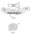
- FIG. 1is a perspective view of a lithographic system in accordance with the present invention
- FIG. 2is a simplified elevation view of a lithographic system shown in FIG. 1 ;
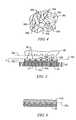
- FIG. 3is a simplified representation of material from which an imprinting layer, shown in FIG. 2 , is comprised before being polymerized and cross-linked;
- FIG. 4is a simplified representation of cross-linked polymer material into which the material shown in FIG. 3 is transformed after being subjected to radiation;
- FIG. 5is a simplified elevation view of a mold spaced-apart from the imprinting layer, shown in FIG. 1 , after patterning of the imprinting layer;
- FIG. 6is a simplified elevation view of an additional imprinting layer positioned atop the substrate shown in FIG. 5 after the pattern in the first imprinting layer is transferred therein;
- FIG. 7is a detailed perspective view of a print head shown in FIG. 1 ;
- FIG. 8is a cross-sectional view of a chucking system in accordance with the present invention.
- FIG. 9is detailed cross-sectional view of an imprint head shown in FIG. 7 ;
- FIG. 10is a bottom-up perspective view of the imprint head shown in FIG. 9 .
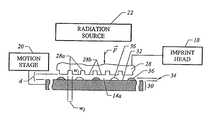
- FIG. 1depicts a lithographic system 10 in accordance with one embodiment of the present invention that includes a pair of spaced-apart bridge supports 12 having a bridge 14 and a stage support 16 extending therebetween. Bridge 14 and stage support 16 are spaced-apart. Coupled to bridge 14 is an imprint head 18 , which extends from bridge 14 toward stage support 16 and provides movement along the Z-axis. Disposed upon stage support 16 to face imprint head 18 is a motion stage 20 . Motion stage 20 is configured to move with respect to stage support 16 along X- and Y-axes.
- imprint head 18may provide movement along the X- and Y-axes, as well as in the Z-axis
- motion stage 20may provide movement in the Z-axis, as well as in the X and Y axes.
- An exemplary motion stage deviceis disclosed in U.S. patent application Ser. No. 10/194,414, filed Jul. 11, 2002, entitled “Step and Repeat Imprint Lithography Systems,” assigned to the assignee of the present invention, and which is incorporated by reference herein in its entirety.
- a radiation source 22is coupled to lithographic system 10 to impinge actinic radiation upon motion stage 20 .
- radiation source 22is coupled to bridge 14 and includes a power generator 23 connected to radiation source 22 .
- Operation of lithographic system 10is typically controlled by a processor 25 that is in data communication therewith.
- Mold 28includes a plurality of features defined by a plurality of spaced-apart recessions 28 a and protrusions 28 b .
- the plurality of featuresdefines an original pattern that is to be transferred into a substrate 30 positioned on motion stage 20 .
- imprint head 18 and/or motion stage 20may vary a distance “d” between mold 28 and substrate 30 .
- the features on mold 28may be imprinted into a flowable region of substrate 30 , discussed more fully below.
- Radiation source 22is located so that mold 28 is positioned between radiation source 22 and substrate 30 .
- mold 28is fabricated from material that allows it to be substantially transparent to the radiation produced by radiation source 22 .
- a flowable regionsuch as an imprinting layer 34 , is disposed on a portion of a surface 32 that presents a substantially planar profile.
- a flowable regionmay be formed using any known technique, such as a hot embossing process disclosed in U.S. Pat. No. 5,772,905, which is incorporated by reference in its entirety herein, or a laser assisted direct imprinting (LADI) process of the type described by Chou et al. in Ultrafast and Direct Imprint of Nanostructures in Silicon , Nature, Col. 417, pp. 835-837, June 2002.
- LADIlaser assisted direct imprinting
- a flowable regionconsists of imprinting layer 34 being deposited as a plurality of spaced-apart discrete droplets 36 of a material 36 a on substrate 30 , discussed more fully below.
- An exemplary system for depositing droplets 36is disclosed in U.S. patent application Ser. No. 10/191,749, filed Jul. 9, 2002, entitled “System and Method for Dispensing Liquids,” assigned to the assignee of the present invention, and which is incorporated by reference herein in its entirety.
- Imprinting layer 34is formed from material 36 a that may be selectively polymerized and cross-linked to record the original pattern therein, defining a recorded pattern.
- An exemplary composition for material 36 ais disclosed in Untied States patent application Ser. No.
- Material 36 ais shown in FIG. 4 as being cross-linked at points 36 b , forming a cross-linked polymer material 36 c.
- the pattern recorded in imprinting layer 34is produced, in part, by mechanical contact with mold 28 .
- distance “d”is reduced to allow droplets 36 to come into mechanical contact with mold 28 , spreading droplets 36 so as to form imprinting layer 34 with a contiguous formation of material 36 a over surface 32 .
- distance “d”is reduced to allow sub-portions 34 a of imprinting layer 34 to ingress into and fill recessions 28 a.
- material 36 ais provided with the requisite properties to completely fill recessions 28 a , while covering surface 32 with a contiguous formation of material 36 a .
- sub-portions 34 b of imprinting layer 34 in superimposition with protrusions 28 bremain after the desired, usually minimum, distance “d” has been reached, leaving sub-portions 34 a with a thickness t 1 , and sub-portions 34 b with a thickness, t 2 .
- Thicknesses “t 1 ” and “t 2 ”may be any thickness desired, dependent upon the application.
- t 1is selected so as to be no greater than twice the width u of sub-portions 34 a , i.e., t 1 ⁇ 2u, shown more clearly in FIG. 5 .
- radiation source 22produces actinic radiation that polymerizes and cross-links material 36 a , forming cross-linked polymer material 36 c .
- the composition of imprinting layer 34transforms from material 36 a to cross-linked polymer material 36 c , which is a solid.
- cross-linked polymer material 36 cis solidified to provide side 34 c of imprinting layer 34 with a shape conforming to a shape of a surface 28 c of mold 28 , shown more clearly in FIG. 5 .
- imprint head 18shown in FIG. 2 , is moved to increase distance “d” so that mold 28 and imprinting layer 34 are spaced-apart.
- substrate 30 and imprinting layer 34may be etched to transfer the pattern of imprinting layer 34 into substrate 30 , providing a patterned surface 32 a , shown in FIG. 6 .
- the material from which imprinting layer 34 is formedmay be varied to define a relative etch rate with respect to substrate 30 , as desired.
- the relative etch rate of imprinting layer 34 to substrate 30may be in a range of about 1.5:1 to about 100:1.
- imprinting layer 34may be provided with an etch differential with respect to photo-resist material (not shown) selectively disposed thereon.
- the photo-resist material (not shown)may be provided to further pattern imprinting layer 34 , using known techniques. Any etch process may be employed, dependent upon the etch rate desired and the underlying constituents that form substrate 30 and imprinting layer 34 . Exemplary etch processes may include plasma etching, reactive ion etching, chemical wet etching and the like.
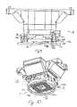
- template 26upon which mold 28 is present, is coupled to an imprint head housing 18 a via a chucking system 40 that includes a chuck body 42 .
- Chuck body 42is adapted to retain template 26 upon which mold 28 is attached employing vacuum techniques.
- chuck body 42includes one or more recesses 42 a that are in fluid communication with a pressure control system, such as a fluid supply system 70 .
- Fluid supply system 70may include one or more pumps to provide both positive and negative pressure, as well as a supply of fluid to facilitate reducing, if not preventing, trapping of gases, such as air, in imprinting layer 34 , shown in FIG. 5 .
- An exemplary chucking systemis disclosed in U.S. patent application Ser. No. 10/293,224, entitled “Chucking System For Modulating Shapes of Substrates,” assigned to the assignee of the present invention, and which is incorporated by reference in its entirety herein.
- template 26is brought into proximity with substrate 30 before patterning imprinting material 36 a is disposed on a region 77 .
- template 26is brought within tens of microns of substrate 30 , e.g., 15 microns more or less. It has been found desirable to perform localized control of the atmosphere 78 that is proximate to both template 26 and region 77 . For example, to avoid the deleterious effects of gases and/or gas pockets present in imprinting material 36 a and/or subsequently trapped in the patterned imprinting layer 34 , it has been found beneficial to control the consistency of fluid in atmosphere 78 and/or the pressure of atmosphere 78 .
- chuck body 42is designed to facilitate the passage of fluids proximate to mold 28 and imprint head 18 includes a baffle 100 surrounding template 26 .
- baffle 100extends from imprint head 18 , terminating in a nadir 102 that lies in a plane in which a surface 26 a lies. In this fashion, mold 28 extends beyond nadir 102 to facilitate contact with region 77 .
- Chuck body 42includes one or more throughways, two of which are shown as 104 and 106 .
- Apertures 104 a and 106 a of throughways 104 and 106are disposed in a surface of chuck body 42 disposed between template 26 and baffle 100 , referred to as a peripheral surface 10 a .
- Throughways 104 and 106place apertures 104 a and 106 a in fluid communication with fluid supply system 70 .
- Baffle 100functions to slow the movement of fluid exiting apertures 104 a and 106 a away from mold 28 .
- baffle 100includes first and second opposed surfaces 102 a and 102 b .
- First opposed surface 102 aextends from nadir 102 away from substrate 30 and faces template 26 .
- Second opposed surface 102 bextends from nadir 102 away from substrate 30 and faces away from mold 28 .
- first opposed surface 102 ais shown extending obliquely with respect to second opposing surface 102 b .
- atmosphere 78may be controlled by introduction or evacuation of fluid through apertures 104 a and 106 a .
- first and second opposed surfaces 102 a and 102 bmay extend parallel to one another from nadir 102 .
- atmosphere 78is established so that the transport of the gases present therein to imprinting material 36 a in region 77 is increased.
- transportis defined to mean any mechanism by which the propagation of gases through imprinting material 36 a is increased, e.g., increased solubility, increased diffusion and the like.
- fluid supply system 70may include a supply of imprinting material 36 a .
- imprinting material 36 amay be introduced through apertures 104 a and 106 a to saturate atmosphere 78 with imprinting material 36 a .
- a difficulty encountered with respect to introducing fluidswas to ensure that the molecules in the fluid streams 104 b and 106 b exiting apertures 104 a and 106 a , respectively, traveled to a region of the atmosphere positioned between mold 28 and droplets 36 , and before contact of droplets 36 with mold 28 .
- This region of atmosphere 78is referred to as a processing region 78 a .
- apertures 104 a and 106 aare disposed about peripheral surface 100 a , which is spaced-apart from processing region 78 a .
- fluid supply system 70under control of processor 25 programmed with suitable control software (not shown) to pulse fluid streams 104 b and 106 b into atmosphere 78 having a desired mixture of molecules, discussed above.
- suitable control softwarenot shown
- laminar flow of fluid streams 104 b and 106 bmay be avoided. It is believed that by providing fluid streams 104 b and 106 b with turbulent flow, the probability will be increased that a sufficient quantity of the molecules contained therein will reach processing region 78 a to reduce, if not avoid, the presence of gases being trapped in imprinting layer 34 (not shown).
- fluidmay be pulsed through both apertures 104 a and 106 a , concurrently, or sequentially pulsed through the same, i.e., first fluid is introduced through aperture 104 a and subsequently through aperture 106 a and then again through 104 a , with the process being repeated for a desired time or during the entire imprinting process.
- the timing of the flow of gas into processing region 78 ais important because it is desired that a sufficient quantity of molecules contained therein reach processing region 78 a before contact is made between mold 28 and droplets 36 .
- fluidmay be pulsed through one of the apertures, e.g., aperture 104 a , and then evacuated through the remaining aperture, e.g., aperture 106 a . In this manner, fluid would be drawn across processing region 78 a . It may also be advantageous to pulse the fluid through both apertures 104 a and 106 a , concurrently, then evacuate through both apertures 104 a and 106 a concurrently. It is desired, however, that the flow rate of fluid be established to minimize, if not avoid, movement of droplets 36 .
- a first stepwould include introducing fluid into atmosphere 78 through both apertures 104 a and 106 a .
- a second stepwould include evacuating the fluid through one of apertures 104 a and 106 a , e.g., aperture 104 a .
- fluidwould be introduced into atmosphere 78 through both apertures 104 a and 106 a , concurrently.
- fluidwould be evacuated through one of apertures 104 a and 106 a that was not employed in the previous step to remove fluid, e.g., aperture 106 a .
- evacuationmay occur through one of apertures 104 a and 106 a , while fluid is being introduced through the remaining aperture of apertures 104 a and 106 a .
- evacuationmay occur in the absence of a fluid flow into atmosphere 78 .
- the desired resultis that fluid ingression into atmosphere 78 and fluid evacuation therefrom occurs so that the desired concentration of fluid is present.
- a plurality of aperturesmay be disposed about peripheral surface 100 a so that each of the apertures of a pair is disposed opposite one another on opposite sides of template 26 . This is shown by aperture pair 104 a and 106 a being disposed opposite one another on opposite sides of template 26 .
- a second aperture pairis shown as 108 a and 110 a .
- Apertures 108 a and 110 aare disposed opposite one another on opposite sides of template 26 .
- each of apertures 104 a , 106 a , 108 a and 110 aare arranged to lie on a common circle with adjacent apertures being spaced-apart therefrom by 90°.
- each of apertures 104 a , 106 a , 108 a and 110 aare arranged to facilitate fluid flow in/out of a different quadrant of chuck body 42 .
- aperture 104 afacilitates fluid flow in/out of quadrant I
- aperture 106 afacilitates fluid flow in/out of quadrant II
- aperture 108 afacilitates fluid flow in/out of quadrant III
- aperture 110 afacilitates fluid flow in/out of quadrant IV.
- any number of aperturesmay be employed, e.g., more than one per quadrant with differing quadrants having differing numbers of apertures and arranged in any spatial arrangement desired.
- Each of these arrangementsshould facilitate introduction and/or evacuation of a plurality of flows of fluid streams into atmosphere 78 , with a subset of the plurality of flows being introduced to differing regions about template 26 . It is believed that introduction of the multiple flows of fluid streams provides a turbulent flow of fluid in atmosphere 78 . This, it is believed, increases the probability that molecules in the fluid streams would reach processing region 78 a , shown in FIG. 9 . However, fluid flow into atmosphere 78 through each of the apertures 104 a , 106 a , 108 a and 110 a and evacuation of fluid from atmosphere 78 therethrough may occur in any manner discussed above.
- a fluid streammay be introduced through each of apertures 104 a , 106 a , 108 a and 110 a sequentially so that a flow cell 112 may be created between template 26 and region 77 .
- Flow cell 112would facilitate ingression of molecules in the fluid streams into processing region 78 a to provide the benefits mentioned above.
- first a fluid flowmay be introduced through aperture 104 a and then terminated. After termination of fluid flow through aperture 104 a , fluid flow through aperture 106 a is commenced to introduce fluid into atmosphere 78 . Subsequently, fluid flow through aperture 106 a is terminated.
- fluid flow through aperture 108 ais commenced to introduce fluid into atmosphere 78 .
- Fluid flow in through aperture 108 ais subsequently terminated.
- fluid flow through aperture 110 ais commenced to introduce fluid into atmosphere 78 .
- fluidis introduced into atmosphere 78 through a single quadrant at any given time.
- sequential introduction and evacuation through apertures 104 a , 106 a , 108 a and 110 amay be undertaken to create flow cell 112 .
- sequential evacuationmay occur through each of apertures 104 a , 106 a , 108 a and 110 a to create flow cell 112 .
- fluidmay be introduced through all apertures in chuck body 42 , concurrently. Thereafter, fluid may be evacuated from each of apertures 104 a , 106 a , 108 a and 110 a , one at a time.
- the concentration in atmosphere 78 of fluid introduced through apertures 104 a , 106 a , 108 a and 110 awent below a desired level due to evacuation.
- the fluidmay then be reintroduced through one or all of apertures 104 a , 106 a , 108 a and 110 a again and the process repeated to create and/or maintain flow cell 112 .
Landscapes
- Engineering & Computer Science (AREA)
- Nanotechnology (AREA)
- Chemical & Material Sciences (AREA)
- Physics & Mathematics (AREA)
- General Physics & Mathematics (AREA)
- Crystallography & Structural Chemistry (AREA)
- Manufacturing & Machinery (AREA)
- Condensed Matter Physics & Semiconductors (AREA)
- Theoretical Computer Science (AREA)
- Mathematical Physics (AREA)
- Microelectronics & Electronic Packaging (AREA)
- Power Engineering (AREA)
- Computer Hardware Design (AREA)
- Shaping Of Tube Ends By Bending Or Straightening (AREA)
- Exposure Of Semiconductors, Excluding Electron Or Ion Beam Exposure (AREA)
Abstract
Description
- The field of invention relates generally to imprint lithography. More particularly, the present invention is directed to reducing pattern distortions during imprint lithography processes by reducing the presence of gases in imprinting layers.
- Micro-fabrication involves the fabrication of very small structures, e.g., having features on the order of micro-meters or smaller. One area in which micro-fabrication has had a sizeable impact is in the processing of integrated circuits. As the semiconductor processing industry continues to strive for larger production yields while increasing the circuits per unit area formed on a substrate, micro-fabrication becomes increasingly important. Micro-fabrication provides greater process control while allowing increased reduction of the minimum feature dimension of the structures formed. Other areas of development in which micro-fabrication has been employed include biotechnology, optical technology, mechanical systems and the like.
- An exemplary micro-fabrication technique is shown in U.S. Pat. No. 6,334,960 to Willson et al. Willson et al. disclose a method of forming a relief image in a structure. The method includes providing a substrate having a transfer layer. The transfer layer is covered with a polymerizable fluid composition. A mold makes mechanical contact with the polymerizable fluid. The mold includes a relief structure, and the polymerizable fluid composition fills the relief structure. The polymerizable fluid composition is then subjected to conditions to solidify and polymerize the same, forming a solidified polymeric material on the transfer layer that contains a relief structure complimentary to that of the mold. The mold is then separated from the solid polymeric material such that a replica of the relief structure in the mold is formed in the solidified polymeric material. The transfer layer and the solidified polymeric material are subjected to an environment to selectively etch the transfer layer relative to the solidified polymeric material such that a relief image is formed in the transfer layer. The time required and the minimum feature dimension provided by this technique is dependent upon, inter alia, the composition of the polymerizable material.
- U.S. Pat. No. 5,772,905 to Chou discloses a lithographic method and apparatus for creating ultra-fine (sub-25 nm) patterns in a thin film coated on a substrate in which a mold having at least one protruding feature is pressed into a thin film carried on a substrate. The protruding feature in the mold creates a recess of the thin film. The mold is removed from the film. The thin film then is processed such that the thin film in the recess is removed, exposing the underlying substrate. Thus, patterns in the mold are replaced in the thin film, completing the lithography. The patterns in the thin film will be, in subsequent processes, reproduced in the substrate or in another material which is added onto the substrate.
- Yet another imprint lithography technique is disclosed by Chou et al. inUltrafast and Direct Imprint of Nanostructures in Silicon, Nature, Col. 417, pp. 835-837, June 2002, which is referred to as a laser assisted direct imprinting (LADI) process. In this process. a region of a substrate is made flowable, e.g., liquefied, by heating the region with the laser. After the region has reached a desired viscosity, a mold, having a pattern thereon, is placed in contact with the region. The flowable region conforms to the profile of the pattern and is then cooled, solidifying the pattern into the substrate. A concern with this technique involves pattern distortions attributable to the presence of gases in the flowable region.
- It is desired, therefore, to provide a system to reduce distortions in patterns formed using imprint lithographic techniques.
- The present invention is directed to a method to reduce pattern distortions by reducing gas pockets present in a layer of viscous liquid deposited on a substrate. To that end, the method includes increasing the transport of the gases disposed proximate to the substrate to the viscous liquid. Specifically, the atmosphere proximate to the substrate is saturated with gases that are either highly soluble, highly diffusive, or both with respect to the viscous liquid being deposited. Additionally, or in lieu of saturating the atmosphere, the pressure of the atmosphere may be reduced. These and other embodiments are described more fully below.
FIG. 1 is a perspective view of a lithographic system in accordance with the present invention;FIG. 2 is a simplified elevation view of a lithographic system shown inFIG. 1 ;FIG. 3 is a simplified representation of material from which an imprinting layer, shown inFIG. 2 , is comprised before being polymerized and cross-linked;FIG. 4 is a simplified representation of cross-linked polymer material into which the material shown inFIG. 3 is transformed after being subjected to radiation;FIG. 5 is a simplified elevation view of a mold spaced-apart from the imprinting layer, shown inFIG. 1 , after patterning of the imprinting layer;FIG. 6 is a simplified elevation view of an additional imprinting layer positioned atop the substrate shown inFIG. 5 after the pattern in the first imprinting layer is transferred therein;FIG. 7 is a detailed perspective view of a print head shown inFIG. 1 ;FIG. 8 is a cross-sectional view of a chucking system in accordance with the present invention;FIG. 9 is detailed cross-sectional view of an imprint head shown inFIG. 7 ; andFIG. 10 is a bottom-up perspective view of the imprint head shown inFIG. 9 .FIG. 1 depicts alithographic system 10 in accordance with one embodiment of the present invention that includes a pair of spaced-apart bridge supports12 having a bridge14 and astage support 16 extending therebetween. Bridge14 andstage support 16 are spaced-apart. Coupled to bridge14 is animprint head 18, which extends from bridge14 towardstage support 16 and provides movement along the Z-axis. Disposed uponstage support 16 to faceimprint head 18 is amotion stage 20.Motion stage 20 is configured to move with respect tostage support 16 along X- and Y-axes. It should be understood thatimprint head 18 may provide movement along the X- and Y-axes, as well as in the Z-axis, andmotion stage 20 may provide movement in the Z-axis, as well as in the X and Y axes. An exemplary motion stage device is disclosed in U.S. patent application Ser. No. 10/194,414, filed Jul. 11, 2002, entitled “Step and Repeat Imprint Lithography Systems,” assigned to the assignee of the present invention, and which is incorporated by reference herein in its entirety. Aradiation source 22 is coupled tolithographic system 10 to impinge actinic radiation uponmotion stage 20. As shown,radiation source 22 is coupled to bridge14 and includes apower generator 23 connected toradiation source 22. Operation oflithographic system 10 is typically controlled by aprocessor 25 that is in data communication therewith.- Referring to both
FIGS. 1 and 2 , connected toimprint head 18 is atemplate 26 having amold 28 thereon.Mold 28 includes a plurality of features defined by a plurality of spaced-apart recessions 28aandprotrusions 28b. The plurality of features defines an original pattern that is to be transferred into asubstrate 30 positioned onmotion stage 20. To that end,imprint head 18 and/ormotion stage 20 may vary a distance “d” betweenmold 28 andsubstrate 30. In this manner, the features onmold 28 may be imprinted into a flowable region ofsubstrate 30, discussed more fully below.Radiation source 22 is located so thatmold 28 is positioned betweenradiation source 22 andsubstrate 30. As a result,mold 28 is fabricated from material that allows it to be substantially transparent to the radiation produced byradiation source 22. - Referring to both
FIGS. 2 and 3 , a flowable region, such as animprinting layer 34, is disposed on a portion of asurface 32 that presents a substantially planar profile. A flowable region may be formed using any known technique, such as a hot embossing process disclosed in U.S. Pat. No. 5,772,905, which is incorporated by reference in its entirety herein, or a laser assisted direct imprinting (LADI) process of the type described by Chou et al. inUltrafast and Direct Imprint of Nanostructures in Silicon, Nature, Col. 417, pp. 835-837, June 2002. In the present embodiment, however, a flowable region consists ofimprinting layer 34 being deposited as a plurality of spaced-apartdiscrete droplets 36 of a material36aonsubstrate 30, discussed more fully below. An exemplary system for depositingdroplets 36 is disclosed in U.S. patent application Ser. No. 10/191,749, filed Jul. 9, 2002, entitled “System and Method for Dispensing Liquids,” assigned to the assignee of the present invention, and which is incorporated by reference herein in its entirety. Imprintinglayer 34 is formed frommaterial 36athat may be selectively polymerized and cross-linked to record the original pattern therein, defining a recorded pattern. An exemplary composition formaterial 36ais disclosed in Untied States patent application Ser. No. 10/463,396, filed Jun. 16, 2003, and entitled “Method to Reduce Adhesion Between a Conformable Region and a Pattern of a Mold,” which is incorporated by reference in its entirety herein.Material 36ais shown inFIG. 4 as being cross-linked atpoints 36b, forming across-linked polymer material 36c. - Referring to
FIGS. 2, 3 and5, the pattern recorded inimprinting layer 34 is produced, in part, by mechanical contact withmold 28. To that end, distance “d” is reduced to allowdroplets 36 to come into mechanical contact withmold 28, spreadingdroplets 36 so as to form imprintinglayer 34 with a contiguous formation ofmaterial 36aoversurface 32. In one embodiment, distance “d” is reduced to allow sub-portions34aofimprinting layer 34 to ingress into and fillrecessions 28a. - To facilitate filling of
recessions 28a,material 36ais provided with the requisite properties to completely fillrecessions 28a, while coveringsurface 32 with a contiguous formation ofmaterial 36a. In the present embodiment, sub-portions34bofimprinting layer 34 in superimposition withprotrusions 28bremain after the desired, usually minimum, distance “d” has been reached, leaving sub-portions34awith a thickness t1, and sub-portions34bwith a thickness, t2. Thicknesses “t1” and “t2” may be any thickness desired, dependent upon the application. Typically, t1is selected so as to be no greater than twice the width u of sub-portions34a, i.e., t1≦2u, shown more clearly inFIG. 5 . - Referring to
FIGS. 2, 3 and4, after a desired distance “d” has been reached,radiation source 22 produces actinic radiation that polymerizes andcross-links material 36a, formingcross-linked polymer material 36c. As a result, the composition ofimprinting layer 34 transforms frommaterial 36atocross-linked polymer material 36c, which is a solid. Specifically,cross-linked polymer material 36cis solidified to provideside 34cofimprinting layer 34 with a shape conforming to a shape of asurface 28cofmold 28, shown more clearly inFIG. 5 . After imprintinglayer 34 is transformed to consist ofcross-linked polymer material 36c, shown inFIG. 4 ,imprint head 18, shown inFIG. 2 , is moved to increase distance “d” so thatmold 28 andimprinting layer 34 are spaced-apart. - Referring to
FIG. 5 , additional processing may be employed to complete the patterning ofsubstrate 30. For example,substrate 30 andimprinting layer 34 may be etched to transfer the pattern ofimprinting layer 34 intosubstrate 30, providing a patternedsurface 32a, shown inFIG. 6 . To facilitate etching, the material from whichimprinting layer 34 is formed may be varied to define a relative etch rate with respect tosubstrate 30, as desired. The relative etch rate ofimprinting layer 34 tosubstrate 30 may be in a range of about 1.5:1 to about 100:1. - Alternatively, or in addition to,
imprinting layer 34 may be provided with an etch differential with respect to photo-resist material (not shown) selectively disposed thereon. The photo-resist material (not shown) may be provided to furtherpattern imprinting layer 34, using known techniques. Any etch process may be employed, dependent upon the etch rate desired and the underlying constituents that formsubstrate 30 andimprinting layer 34. Exemplary etch processes may include plasma etching, reactive ion etching, chemical wet etching and the like. - Referring to
FIGS. 7 and 8 ,template 26, upon whichmold 28 is present, is coupled to an imprint head housing18avia achucking system 40 that includes achuck body 42. Chuckbody 42 is adapted to retaintemplate 26 upon whichmold 28 is attached employing vacuum techniques. To that end, chuckbody 42 includes one ormore recesses 42athat are in fluid communication with a pressure control system, such as afluid supply system 70.Fluid supply system 70 may include one or more pumps to provide both positive and negative pressure, as well as a supply of fluid to facilitate reducing, if not preventing, trapping of gases, such as air, inimprinting layer 34, shown inFIG. 5 . An exemplary chucking system is disclosed in U.S. patent application Ser. No. 10/293,224, entitled “Chucking System For Modulating Shapes of Substrates,” assigned to the assignee of the present invention, and which is incorporated by reference in its entirety herein. - As discussed above, during imprinting
template 26 and, therefore,mold 28 are brought into proximity withsubstrate 30 before patterningimprinting material 36ais disposed on a region77. Specifically,template 26 is brought within tens of microns ofsubstrate 30, e.g., 15 microns more or less. It has been found desirable to perform localized control of theatmosphere 78 that is proximate to bothtemplate 26 and region77. For example, to avoid the deleterious effects of gases and/or gas pockets present in imprintingmaterial 36aand/or subsequently trapped in the patternedimprinting layer 34, it has been found beneficial to control the consistency of fluid inatmosphere 78 and/or the pressure ofatmosphere 78. - Referring to
FIG. 9 , to facilitate control ofatmosphere 78,chuck body 42 is designed to facilitate the passage of fluids proximate to mold28 andimprint head 18 includes abaffle 100 surroundingtemplate 26. Specifically, baffle100 extends fromimprint head 18, terminating in anadir 102 that lies in a plane in which a surface26alies. In this fashion,mold 28 extends beyondnadir 102 to facilitate contact with region77. Chuckbody 42 includes one or more throughways, two of which are shown as104 and106.Apertures 104aand106aofthroughways chuck body 42 disposed betweentemplate 26 andbaffle 100, referred to as a peripheral surface10a.Throughways place apertures 104aand106ain fluid communication withfluid supply system 70.Baffle 100 functions to slow the movement offluid exiting apertures 104aand106aaway frommold 28. To that end,baffle 100 includes first and secondopposed surfaces 102aand102b. First opposed surface102aextends fromnadir 102 away fromsubstrate 30 and facestemplate 26. Secondopposed surface 102bextends fromnadir 102 away fromsubstrate 30 and faces away frommold 28. Although it is not necessary, first opposed surface102ais shown extending obliquely with respect to second opposingsurface 102b. With this configuration,atmosphere 78 may be controlled by introduction or evacuation of fluid throughapertures 104aand106a. However, first and secondopposed surfaces 102aand102bmay extend parallel to one another fromnadir 102. - Referring to
FIGS. 3 and 9 , in one embodiment,atmosphere 78 is established so that the transport of the gases present therein to imprinting material36ain region77 is increased. The term transport is defined to mean any mechanism by which the propagation of gases through imprintingmaterial 36ais increased, e.g., increased solubility, increased diffusion and the like. To that end,fluid supply system 70 may include a supply ofimprinting material 36a. Under control ofprocessor 25, which is in data communication withfluid supply system 70, imprintingmaterial 36amay be introduced throughapertures 104aand106ato saturateatmosphere 78 withimprinting material 36a. This was found to reduce, if not completely do away with, the quantity of gases, such as air, trapped in theimprinting layer 34 during imprint processes. This is beneficial as it was found that the presence of air inimprinting layer 34 creates undesirable voids. Alternatively, it was found that by saturatingatmosphere 78 with carbon dioxide and/or helium the quantity of air trapped inimprinting layer 34, shown inFIG. 5 , was substantially reduced if not avoided. It should be understood that a mixture of imprintingmaterial 36a, shown inFIG. 3 , carbon dioxide and/or helium may be introduced intoatmosphere 78, shown inFIG. 9 , to reduce the quantity of air trapped inimprinting layer 34, shown inFIG. 5 . - Referring to
FIGS. 9 and 10 , a difficulty encountered with respect to introducing fluids was to ensure that the molecules in the fluid streams104band106bexitingapertures 104aand106a, respectively, traveled to a region of the atmosphere positioned betweenmold 28 anddroplets 36, and before contact ofdroplets 36 withmold 28. This region ofatmosphere 78 is referred to as a processing region78a. As shown,apertures 104aand106aare disposed aboutperipheral surface 100a, which is spaced-apart from processing region78a. Given that the separation ofmold 28 from region77 is on the order of microns, the relative dimensions of the molecules in fluid streams104band106band the spacing betweenmold 28 and region77 makes difficult the ingression of the aforementioned molecules into processing region78a. - One manner in which to overcome the aforementioned difficulty is to have
fluid supply system 70 under control ofprocessor 25 programmed with suitable control software (not shown) to pulse fluid streams104band106bintoatmosphere 78 having a desired mixture of molecules, discussed above. In this manner, laminar flow of fluid streams104band106bmay be avoided. It is believed that by providing fluid streams104band106bwith turbulent flow, the probability will be increased that a sufficient quantity of the molecules contained therein will reach processing region78ato reduce, if not avoid, the presence of gases being trapped in imprinting layer34 (not shown). To that end, fluid may be pulsed through bothapertures 104aand106a, concurrently, or sequentially pulsed through the same, i.e., first fluid is introduced through aperture104aand subsequently throughaperture 106aand then again through104a, with the process being repeated for a desired time or during the entire imprinting process. Furthermore, the timing of the flow of gas into processing region78ais important because it is desired that a sufficient quantity of molecules contained therein reach processing region78abefore contact is made betweenmold 28 anddroplets 36. - Alternatively, fluid may be pulsed through one of the apertures, e.g., aperture104a, and then evacuated through the remaining aperture, e.g.,
aperture 106a. In this manner, fluid would be drawn across processing region78a. It may also be advantageous to pulse the fluid through bothapertures 104aand106a, concurrently, then evacuate through bothapertures 104aand106aconcurrently. It is desired, however, that the flow rate of fluid be established to minimize, if not avoid, movement ofdroplets 36. - To ensure that the
fluids exiting apertures 104aand106acrosses through processing region78a, it may be advantageous to concurrently pulse fluid through bothapertures 104aand106aconcurrently and then alternatingly evacuate through one ofapertures 104aor106a. Concurrently introducing the fluid through bothapertures 104aand106aminimizes the time required to saturateatmosphere 78. Alternatingly evacuating the fluid through one ofapertures 104aand106aensures that the fluid travels through processing region78a. For example, a first step would include introducing fluid intoatmosphere 78 through bothapertures 104aand106a. A second step would include evacuating the fluid through one ofapertures 104aand106a, e.g., aperture104a. Thereafter, at a third step, fluid would be introduced intoatmosphere 78 through bothapertures 104aand106a, concurrently. At a fourth step, fluid would be evacuated through one ofapertures 104aand106athat was not employed in the previous step to remove fluid, e.g.,aperture 106a. It should be understood that evacuation may occur through one ofapertures 104aand106a, while fluid is being introduced through the remaining aperture ofapertures 104aand106a. Alternatively, evacuation may occur in the absence of a fluid flow intoatmosphere 78. The desired result is that fluid ingression intoatmosphere 78 and fluid evacuation therefrom occurs so that the desired concentration of fluid is present. - In another embodiment, a plurality of apertures may be disposed about
peripheral surface 100aso that each of the apertures of a pair is disposed opposite one another on opposite sides oftemplate 26. This is shown byaperture pair 104aand106abeing disposed opposite one another on opposite sides oftemplate 26. A second aperture pair is shown as108aand110a. Apertures108aand110aare disposed opposite one another on opposite sides oftemplate 26. - As shown, each of
apertures 104a,106a,108aand110a, are arranged to lie on a common circle with adjacent apertures being spaced-apart therefrom by 90°. In this manner, each ofapertures 104a,106a,108aand110aare arranged to facilitate fluid flow in/out of a different quadrant ofchuck body 42. Specifically, aperture104afacilitates fluid flow in/out of quadrant I;aperture 106afacilitates fluid flow in/out of quadrant II; aperture108afacilitates fluid flow in/out of quadrant III; and aperture110afacilitates fluid flow in/out of quadrant IV. However, any number of apertures may be employed, e.g., more than one per quadrant with differing quadrants having differing numbers of apertures and arranged in any spatial arrangement desired. Each of these arrangements should facilitate introduction and/or evacuation of a plurality of flows of fluid streams intoatmosphere 78, with a subset of the plurality of flows being introduced to differing regions abouttemplate 26. It is believed that introduction of the multiple flows of fluid streams provides a turbulent flow of fluid inatmosphere 78. This, it is believed, increases the probability that molecules in the fluid streams would reach processing region78a, shown inFIG. 9 . However, fluid flow intoatmosphere 78 through each of theapertures 104a,106a,108aand110aand evacuation of fluid fromatmosphere 78 therethrough may occur in any manner discussed above. - Referring to
FIGS. 9, 10 and11, in another embodiment, a fluid stream may be introduced through each ofapertures 104a,106a,108aand110asequentially so that aflow cell 112 may be created betweentemplate 26 and region77.Flow cell 112 would facilitate ingression of molecules in the fluid streams into processing region78ato provide the benefits mentioned above. For example, first a fluid flow may be introduced through aperture104aand then terminated. After termination of fluid flow through aperture104a, fluid flow throughaperture 106ais commenced to introduce fluid intoatmosphere 78. Subsequently, fluid flow throughaperture 106ais terminated. After termination of fluid flow throughaperture 106a, fluid flow through aperture108ais commenced to introduce fluid intoatmosphere 78. Fluid flow in through aperture108ais subsequently terminated. After termination of fluid flow through aperture108a, fluid flow through aperture110ais commenced to introduce fluid intoatmosphere 78. In this manner, fluid is introduced intoatmosphere 78 through a single quadrant at any given time. However, it may be desirable to introduce fluid into more than one quadrant. Although this may frustrate creation offlow cell 112, it is within confines of the present invention. - Alternatively, sequential introduction and evacuation through
apertures 104a,106a,108aand110amay be undertaken to createflow cell 112. This would include introducing fluid through one or more ofapertures 104a,106a,108aand110a, concurrently. Subsequently, sequential evacuation may occur through each ofapertures 104a,106a,108aand110ato createflow cell 112. For example, fluid may be introduced through all apertures inchuck body 42, concurrently. Thereafter, fluid may be evacuated from each ofapertures 104a,106a,108aand110a, one at a time. Before, the concentration inatmosphere 78 of fluid introduced throughapertures 104a,106a,108aand110awent below a desired level due to evacuation. The fluid may then be reintroduced through one or all ofapertures 104a,106a,108aand110aagain and the process repeated to create and/or maintainflow cell 112. - The embodiments of the present invention described above are exemplary. Many changes and modifications may be made to the disclosure recited above, while remaining within the scope of the invention. Therefore, the scope of the invention should not be limited by the above description, but instead should be determined with reference to the appended claims along with their full scope of equivalents.
Claims (25)
Priority Applications (17)
| Application Number | Priority Date | Filing Date | Title |
|---|---|---|---|
| US10/677,639US7090716B2 (en) | 2003-10-02 | 2003-10-02 | Single phase fluid imprint lithography method |
| US10/898,037US7270533B2 (en) | 2003-10-02 | 2004-07-23 | System for creating a turbulent flow of fluid between a mold and a substrate |
| US10/898,034US7531025B2 (en) | 2003-10-02 | 2004-07-23 | Method of creating a turbulent flow of fluid between a mold and a substrate |
| PCT/US2004/031408WO2005033797A2 (en) | 2003-10-02 | 2004-09-24 | Single phase fluid imprint lithography method |
| SG200608694ASG128681A1 (en) | 2003-10-02 | 2004-09-24 | Single phase fluid imprint lithography method |
| EP04817123AEP1667778B1 (en) | 2003-10-02 | 2004-09-24 | Single phase fluid imprint lithography method |
| KR1020127011488AKR101241076B1 (en) | 2003-10-02 | 2004-09-24 | Single phase fluid imprint lithography method |
| CNB2004800285602ACN100482307C (en) | 2003-10-02 | 2004-09-24 | Method of reducing gas in a viscous fluid layer on a gasket |
| JP2006533980AJP2007509769A (en) | 2003-10-02 | 2004-09-24 | Single phase fluid imprint lithography |
| KR1020067006082AKR20060096424A (en) | 2003-10-02 | 2004-09-24 | Single Phase Fluid Imprint Lithography Method |
| KR1020117022529AKR101178432B1 (en) | 2003-10-02 | 2004-09-24 | Single phase fluid imprint lithography method |
| MYPI20043967AMY135469A (en) | 2003-10-02 | 2004-09-28 | Single phase fluid imprint lithography method |
| TW093129415ATWI250560B (en) | 2003-10-02 | 2004-09-29 | Single phase fluid imprint lithography method |
| US12/026,022US8211214B2 (en) | 2003-10-02 | 2008-02-05 | Single phase fluid imprint lithography method |
| JP2010077189AJP4658227B2 (en) | 2003-10-02 | 2010-03-30 | Single phase fluid imprint lithography |
| JP2010077193AJP4536157B1 (en) | 2003-10-02 | 2010-03-30 | Single phase fluid imprint lithography |
| JP2011090191AJP5275399B2 (en) | 2003-10-02 | 2011-04-14 | Method for reducing the gas trapped in an imprint layer |
Applications Claiming Priority (1)
| Application Number | Priority Date | Filing Date | Title |
|---|---|---|---|
| US10/677,639US7090716B2 (en) | 2003-10-02 | 2003-10-02 | Single phase fluid imprint lithography method |
Related Child Applications (2)
| Application Number | Title | Priority Date | Filing Date |
|---|---|---|---|
| US10/898,037DivisionUS7270533B2 (en) | 2003-10-02 | 2004-07-23 | System for creating a turbulent flow of fluid between a mold and a substrate |
| US10/898,034DivisionUS7531025B2 (en) | 2003-10-02 | 2004-07-23 | Method of creating a turbulent flow of fluid between a mold and a substrate |
Publications (2)
| Publication Number | Publication Date |
|---|---|
| US20050072755A1true US20050072755A1 (en) | 2005-04-07 |
| US7090716B2 US7090716B2 (en) | 2006-08-15 |
Family
ID=34393769
Family Applications (3)
| Application Number | Title | Priority Date | Filing Date |
|---|---|---|---|
| US10/677,639Expired - LifetimeUS7090716B2 (en) | 2003-10-02 | 2003-10-02 | Single phase fluid imprint lithography method |
| US10/898,037Expired - LifetimeUS7270533B2 (en) | 2003-10-02 | 2004-07-23 | System for creating a turbulent flow of fluid between a mold and a substrate |
| US10/898,034Expired - Fee RelatedUS7531025B2 (en) | 2003-10-02 | 2004-07-23 | Method of creating a turbulent flow of fluid between a mold and a substrate |
Family Applications After (2)
| Application Number | Title | Priority Date | Filing Date |
|---|---|---|---|
| US10/898,037Expired - LifetimeUS7270533B2 (en) | 2003-10-02 | 2004-07-23 | System for creating a turbulent flow of fluid between a mold and a substrate |
| US10/898,034Expired - Fee RelatedUS7531025B2 (en) | 2003-10-02 | 2004-07-23 | Method of creating a turbulent flow of fluid between a mold and a substrate |
Country Status (9)
| Country | Link |
|---|---|
| US (3) | US7090716B2 (en) |
| EP (1) | EP1667778B1 (en) |
| JP (4) | JP2007509769A (en) |
| KR (3) | KR20060096424A (en) |
| CN (1) | CN100482307C (en) |
| MY (1) | MY135469A (en) |
| SG (1) | SG128681A1 (en) |
| TW (1) | TWI250560B (en) |
| WO (1) | WO2005033797A2 (en) |
Cited By (26)
| Publication number | Priority date | Publication date | Assignee | Title |
|---|---|---|---|---|
| US20050072757A1 (en)* | 2003-10-02 | 2005-04-07 | University Of Texas System Board Of Regents | Method of creating a turbulent flow of fluid between a mold and a substrate |
| US20050084804A1 (en)* | 2003-10-16 | 2005-04-21 | Molecular Imprints, Inc. | Low surface energy templates |
| US20060063359A1 (en)* | 2004-09-21 | 2006-03-23 | Molecular Imprints, Inc. | Patterning substrates employing multi-film layers defining etch differential interfaces |
| US20060105571A1 (en)* | 2004-11-16 | 2006-05-18 | International Business Machines Corporation | Pneumatic method and apparatus for nano imprint lithography |
| US20070063384A1 (en)* | 2005-09-21 | 2007-03-22 | Molecular Imprints, Inc. | Method to control an atmostphere between a body and a substrate |
| US20080174046A1 (en)* | 2002-07-11 | 2008-07-24 | Molecular Imprints Inc. | Capillary Imprinting Technique |
| US20090057267A1 (en)* | 2007-09-05 | 2009-03-05 | Asml Netherlands B.V. | Imprint lithography |
| WO2009099630A1 (en)* | 2008-02-05 | 2009-08-13 | Molecular Imprints, Inc. | Single phase fluid imprint lithography method |
| EP1958025A4 (en)* | 2005-12-08 | 2009-10-21 | Molecular Imprints Inc | METHOD FOR EJECTING BETWEEN A SUBSTRATE AND A FORM OF ARRANGED GAS |
| US20100096764A1 (en)* | 2008-10-20 | 2010-04-22 | Molecular Imprints, Inc. | Gas Environment for Imprint Lithography |
| WO2011050817A1 (en)* | 2009-11-02 | 2011-05-05 | Danmarks Tekniske Universitet | Method and device for nanoimprint lithography |
| US20110140304A1 (en)* | 2009-12-10 | 2011-06-16 | Molecular Imprints, Inc. | Imprint lithography template |
| US20110193251A1 (en)* | 2010-02-09 | 2011-08-11 | Molecular Imprints, Inc. | Process Gas Confinement for Nano-Imprinting |
| US20110290136A1 (en)* | 2010-05-31 | 2011-12-01 | Canon Kabushiki Kaisha | Lithographic apparatus and manufacturing method of commodities |
| US20120007280A1 (en)* | 2009-02-27 | 2012-01-12 | Hitachi High-Technologies Corporation | Fine-structure transfer method |
| US20120080820A1 (en)* | 2010-10-04 | 2012-04-05 | Canon Kabushiki Kaisha | Imprinting method |
| US20140312532A1 (en)* | 2013-04-18 | 2014-10-23 | Canon Kabushiki Kaisha | Imprint apparatus and article manufacturing method |
| CN104823264A (en)* | 2012-11-30 | 2015-08-05 | 佳能株式会社 | Imprint method and curable composition for imprint |
| WO2015141604A1 (en)* | 2014-03-17 | 2015-09-24 | Canon Kabushiki Kaisha | Imprint apparatus and method of manufacturing article |
| JP2016086190A (en)* | 2012-01-19 | 2016-05-19 | キヤノン株式会社 | Imprint method, and imprint device |
| US9636851B2 (en) | 2011-02-07 | 2017-05-02 | Canon Kabushiki Kaisha | Imprint apparatus and article manufacturing method |
| US10279538B2 (en) | 2012-10-04 | 2019-05-07 | Dai Nippon Printing Co., Ltd. | Imprinting method and imprinting apparatus |
| US11121322B2 (en) | 2015-10-12 | 2021-09-14 | Universal Display Corporation | Apparatus and method to deliver organic material via organic vapor-jet printing (OVJP) |
| US11220737B2 (en) | 2014-06-25 | 2022-01-11 | Universal Display Corporation | Systems and methods of modulating flow during vapor jet deposition of organic materials |
| US11267012B2 (en)* | 2014-06-25 | 2022-03-08 | Universal Display Corporation | Spatial control of vapor condensation using convection |
| US11591686B2 (en) | 2014-06-25 | 2023-02-28 | Universal Display Corporation | Methods of modulating flow during vapor jet deposition of organic materials |
Families Citing this family (59)
| Publication number | Priority date | Publication date | Assignee | Title |
|---|---|---|---|---|
| US20010030511A1 (en) | 2000-04-18 | 2001-10-18 | Shunpei Yamazaki | Display device |
| US20080160129A1 (en)* | 2006-05-11 | 2008-07-03 | Molecular Imprints, Inc. | Template Having a Varying Thickness to Facilitate Expelling a Gas Positioned Between a Substrate and the Template |
| US7019819B2 (en) | 2002-11-13 | 2006-03-28 | Molecular Imprints, Inc. | Chucking system for modulating shapes of substrates |
| US7077992B2 (en)* | 2002-07-11 | 2006-07-18 | Molecular Imprints, Inc. | Step and repeat imprint lithography processes |
| US7641840B2 (en)* | 2002-11-13 | 2010-01-05 | Molecular Imprints, Inc. | Method for expelling gas positioned between a substrate and a mold |
| US20070164476A1 (en)* | 2004-09-01 | 2007-07-19 | Wei Wu | Contact lithography apparatus and method employing substrate deformation |
| US7641468B2 (en)* | 2004-09-01 | 2010-01-05 | Hewlett-Packard Development Company, L.P. | Imprint lithography apparatus and method employing an effective pressure |
| US20060062922A1 (en)* | 2004-09-23 | 2006-03-23 | Molecular Imprints, Inc. | Polymerization technique to attenuate oxygen inhibition of solidification of liquids and composition therefor |
| US20060081557A1 (en) | 2004-10-18 | 2006-04-20 | Molecular Imprints, Inc. | Low-k dielectric functional imprinting materials |
| US7377764B2 (en) | 2005-06-13 | 2008-05-27 | Asml Netherlands B.V. | Imprint lithography |
| US7906058B2 (en) | 2005-12-01 | 2011-03-15 | Molecular Imprints, Inc. | Bifurcated contact printing technique |
| US7670530B2 (en) | 2006-01-20 | 2010-03-02 | Molecular Imprints, Inc. | Patterning substrates employing multiple chucks |
| MY144847A (en) | 2005-12-08 | 2011-11-30 | Molecular Imprints Inc | Method and system for double-sided patterning of substrates |
| US20070138699A1 (en)* | 2005-12-21 | 2007-06-21 | Asml Netherlands B.V. | Imprint lithography |
| KR20080114681A (en)* | 2006-04-03 | 2008-12-31 | 몰레큘러 임프린츠 인코퍼레이티드 | Lithography Imprinting System |
| US8012395B2 (en) | 2006-04-18 | 2011-09-06 | Molecular Imprints, Inc. | Template having alignment marks formed of contrast material |
| US8215946B2 (en) | 2006-05-18 | 2012-07-10 | Molecular Imprints, Inc. | Imprint lithography system and method |
| DE102006024524A1 (en)* | 2006-05-23 | 2007-12-06 | Von Ardenne Anlagentechnik Gmbh | Transparent multi-layer composite system capable of reflecting infrared radiation for hardening and/or shaping of substrates and temperature process, comprises layers, anti-reflection coating, blocking layer and dielectric interface layer |
| TW200842934A (en)* | 2006-12-29 | 2008-11-01 | Molecular Imprints Inc | Imprint fluid control |
| US20090014917A1 (en)* | 2007-07-10 | 2009-01-15 | Molecular Imprints, Inc. | Drop Pattern Generation for Imprint Lithography |
| US8119052B2 (en)* | 2007-11-02 | 2012-02-21 | Molecular Imprints, Inc. | Drop pattern generation for imprint lithography |
| SG185929A1 (en)* | 2007-11-21 | 2012-12-28 | Molecular Imprints Inc | Porous template and imprinting stack for nano-imprint lithography |
| US8945444B2 (en)* | 2007-12-04 | 2015-02-03 | Canon Nanotechnologies, Inc. | High throughput imprint based on contact line motion tracking control |
| TW200932502A (en)* | 2008-01-18 | 2009-08-01 | Univ Nat Taiwan | An improved embossing apparatus |
| US8361371B2 (en)* | 2008-02-08 | 2013-01-29 | Molecular Imprints, Inc. | Extrusion reduction in imprint lithography |
| US8187515B2 (en)* | 2008-04-01 | 2012-05-29 | Molecular Imprints, Inc. | Large area roll-to-roll imprint lithography |
| US20100072671A1 (en)* | 2008-09-25 | 2010-03-25 | Molecular Imprints, Inc. | Nano-imprint lithography template fabrication and treatment |
| US8470188B2 (en)* | 2008-10-02 | 2013-06-25 | Molecular Imprints, Inc. | Nano-imprint lithography templates |
| US8586126B2 (en) | 2008-10-21 | 2013-11-19 | Molecular Imprints, Inc. | Robust optimization to generate drop patterns in imprint lithography which are tolerant of variations in drop volume and drop placement |
| US8512797B2 (en)* | 2008-10-21 | 2013-08-20 | Molecular Imprints, Inc. | Drop pattern generation with edge weighting |
| US20100104852A1 (en)* | 2008-10-23 | 2010-04-29 | Molecular Imprints, Inc. | Fabrication of High-Throughput Nano-Imprint Lithography Templates |
| US20100112220A1 (en)* | 2008-11-03 | 2010-05-06 | Molecular Imprints, Inc. | Dispense system set-up and characterization |
| WO2010063504A2 (en)* | 2008-12-04 | 2010-06-10 | Asml Netherlands B.V. | Imprint lithography apparatus and method |
| WO2010111307A1 (en)* | 2009-03-23 | 2010-09-30 | Intevac, Inc. | A process for optimization of island to trench ratio in patterned media |
| JP2011023660A (en)* | 2009-07-17 | 2011-02-03 | Toshiba Corp | Pattern transfer method |
| US8616873B2 (en)* | 2010-01-26 | 2013-12-31 | Molecular Imprints, Inc. | Micro-conformal templates for nanoimprint lithography |
| US20110180964A1 (en)* | 2010-01-27 | 2011-07-28 | Molecular Imprints. Inc. | Systems and methods for substrate formation |
| TW201144091A (en)* | 2010-01-29 | 2011-12-16 | Molecular Imprints Inc | Ultra-compliant nanoimprint lithography templates |
| JP5491931B2 (en)* | 2010-03-30 | 2014-05-14 | 富士フイルム株式会社 | Nanoimprint method and mold manufacturing method |
| JP5787691B2 (en)* | 2011-09-21 | 2015-09-30 | キヤノン株式会社 | Imprint apparatus and article manufacturing method using the same |
| US9278857B2 (en) | 2012-01-31 | 2016-03-08 | Seagate Technology Inc. | Method of surface tension control to reduce trapped gas bubbles |
| JP6304921B2 (en)* | 2012-06-05 | 2018-04-04 | キヤノン株式会社 | Imprint method, imprint apparatus, and article manufacturing method using the same |
| KR102056902B1 (en) | 2013-05-29 | 2019-12-18 | 삼성전자주식회사 | Wire grid polarizer and liquid crystal display panel and liquid crystal display device having the same |
| KR102089661B1 (en) | 2013-08-27 | 2020-03-17 | 삼성전자주식회사 | Wire grid polarizer and liquid crystal display panel and liquid crystal display device having the same |
| JP5865332B2 (en) | 2013-11-01 | 2016-02-17 | キヤノン株式会社 | Imprint apparatus, article manufacturing method, and imprint method |
| CN105706214B (en)* | 2013-11-06 | 2018-10-02 | 佳能株式会社 | Method, method for stamping and the device of pattern for determining imprint mold |
| JP6294679B2 (en) | 2014-01-21 | 2018-03-14 | キヤノン株式会社 | Imprint apparatus and article manufacturing method |
| JP2015005760A (en)* | 2014-07-31 | 2015-01-08 | キヤノン株式会社 | Imprint device, and article manufacturing method |
| JP6525567B2 (en) | 2014-12-02 | 2019-06-05 | キヤノン株式会社 | Imprint apparatus and method of manufacturing article |
| JP6628491B2 (en) | 2015-04-13 | 2020-01-08 | キヤノン株式会社 | Imprint apparatus, imprint method, and article manufacturing method |
| JP5989177B2 (en)* | 2015-04-20 | 2016-09-07 | キヤノン株式会社 | Imprint apparatus and article manufacturing method |
| KR101968471B1 (en) | 2017-01-30 | 2019-04-11 | 배용주 | Equipment for generation and saving the electricity |
| US10895806B2 (en)* | 2017-09-29 | 2021-01-19 | Canon Kabushiki Kaisha | Imprinting method and apparatus |
| US10684407B2 (en)* | 2017-10-30 | 2020-06-16 | Facebook Technologies, Llc | Reactivity enhancement in ion beam etcher |
| JP7210155B2 (en) | 2018-04-16 | 2023-01-23 | キヤノン株式会社 | Apparatus, methods, and methods of making articles |
| US11137536B2 (en) | 2018-07-26 | 2021-10-05 | Facebook Technologies, Llc | Bragg-like gratings on high refractive index material |
| US11226446B2 (en) | 2020-05-06 | 2022-01-18 | Facebook Technologies, Llc | Hydrogen/nitrogen doping and chemically assisted etching of high refractive index gratings |
| US11590687B2 (en) | 2020-06-30 | 2023-02-28 | Canon Kabushiki Kaisha | Systems and methods for reducing pressure while shaping a film |
| CN118605080B (en)* | 2024-06-18 | 2025-05-27 | 联合微电子中心有限责任公司 | Nanoimprint method and nanoimprint mold |
Citations (91)
| Publication number | Priority date | Publication date | Assignee | Title |
|---|---|---|---|---|
| US3783520A (en)* | 1970-09-28 | 1974-01-08 | Bell Telephone Labor Inc | High accuracy alignment procedure utilizing moire patterns |
| US4070116A (en)* | 1975-06-23 | 1978-01-24 | International Business Machines Corporation | Gap measuring device for defining the distance between two or more surfaces |
| US4201800A (en)* | 1978-04-28 | 1980-05-06 | International Business Machines Corp. | Hardened photoresist master image mask process |
| US4267212A (en)* | 1978-09-20 | 1981-05-12 | Fuji Photo Film Co., Ltd. | Spin coating process |
| US4426247A (en)* | 1982-04-12 | 1984-01-17 | Nippon Telegraph & Telephone Public Corporation | Method for forming micropattern |
| US4451507A (en)* | 1982-10-29 | 1984-05-29 | Rca Corporation | Automatic liquid dispensing apparatus for spinning surface of uniform thickness |
| US4507331A (en)* | 1983-12-12 | 1985-03-26 | International Business Machines Corporation | Dry process for forming positive tone micro patterns |
| US4512848A (en)* | 1984-02-06 | 1985-04-23 | Exxon Research And Engineering Co. | Procedure for fabrication of microstructures over large areas using physical replication |
| US4600309A (en)* | 1982-12-30 | 1986-07-15 | Thomson-Csf | Process and apparatus for theoptical alignment of patterns in two close-up planes in an exposure means incorporating a divergent radiation source |
| US4657845A (en)* | 1986-01-14 | 1987-04-14 | International Business Machines Corporation | Positive tone oxygen plasma developable photoresist |
| US4731155A (en)* | 1987-04-15 | 1988-03-15 | General Electric Company | Process for forming a lithographic mask |
| US4737425A (en)* | 1986-06-10 | 1988-04-12 | International Business Machines Corporation | Patterned resist and process |
| US4808511A (en)* | 1987-05-19 | 1989-02-28 | International Business Machines Corporation | Vapor phase photoresist silylation process |
| US4826943A (en)* | 1986-07-25 | 1989-05-02 | Oki Electric Industry Co., Ltd. | Negative resist material |
| US4848911A (en)* | 1986-06-11 | 1989-07-18 | Kabushiki Kaisha Toshiba | Method for aligning first and second objects, relative to each other, and apparatus for practicing this method |
| US4891303A (en)* | 1988-05-26 | 1990-01-02 | Texas Instruments Incorporated | Trilayer microlithographic process using a silicon-based resist as the middle layer |
| US4908298A (en)* | 1985-03-19 | 1990-03-13 | International Business Machines Corporation | Method of creating patterned multilayer films for use in production of semiconductor circuits and systems |
| US4919748A (en)* | 1989-06-30 | 1990-04-24 | At&T Bell Laboratories | Method for tapered etching |
| US4921778A (en)* | 1988-07-29 | 1990-05-01 | Shipley Company Inc. | Photoresist pattern fabrication employing chemically amplified metalized material |
| US4931351A (en)* | 1987-01-12 | 1990-06-05 | Eastman Kodak Company | Bilayer lithographic process |
| US4999280A (en)* | 1989-03-17 | 1991-03-12 | International Business Machines Corporation | Spray silylation of photoresist images |
| US5028366A (en)* | 1988-01-12 | 1991-07-02 | Air Products And Chemicals, Inc. | Water based mold release compositions for making molded polyurethane foam |
| US5108875A (en)* | 1988-07-29 | 1992-04-28 | Shipley Company Inc. | Photoresist pattern fabrication employing chemically amplified metalized material |
| US5179863A (en)* | 1990-03-05 | 1993-01-19 | Kabushiki Kaisha Toshiba | Method and apparatus for setting the gap distance between a mask and a wafer at a predetermined distance |
| US5198326A (en)* | 1990-05-24 | 1993-03-30 | Matsushita Electric Industrial Co., Ltd. | Process for forming fine pattern |
| US5212147A (en)* | 1991-05-15 | 1993-05-18 | Hewlett-Packard Company | Method of forming a patterned in-situ high Tc superconductive film |
| US5314772A (en)* | 1990-10-09 | 1994-05-24 | Arizona Board Of Regents | High resolution, multi-layer resist for microlithography and method therefor |
| US5318870A (en)* | 1989-10-18 | 1994-06-07 | Massachusetts Institute Of Technology | Method of patterning a phenolic polymer film without photoactive additive through exposure to high energy radiation below 225 nm with subsequent organometallic treatment and the associated imaged article |
| US5324683A (en)* | 1993-06-02 | 1994-06-28 | Motorola, Inc. | Method of forming a semiconductor structure having an air region |
| US5328810A (en)* | 1990-05-07 | 1994-07-12 | Micron Technology, Inc. | Method for reducing, by a factor or 2-N, the minimum masking pitch of a photolithographic process |
| US5330881A (en)* | 1989-06-02 | 1994-07-19 | Digital Equipment Corp. | Microlithographic method for producing thick, vertically-walled photoresist patterns |
| US5380474A (en)* | 1993-05-20 | 1995-01-10 | Sandia Corporation | Methods for patterned deposition on a substrate |
| US5417802A (en)* | 1994-03-18 | 1995-05-23 | At&T Corp. | Integrated circuit manufacturing |
| US5422295A (en)* | 1992-12-10 | 1995-06-06 | Samsung Electronics Co., Ltd. | Method for forming a semiconductor memory device having a vertical multi-layered storage electrode |
| US5421981A (en)* | 1991-06-26 | 1995-06-06 | Ppg Industries, Inc. | Electrochemical sensor storage device |
| US5424549A (en)* | 1991-12-20 | 1995-06-13 | Board Of Supervisors Of Louisiana State University And Agricultural And Mechanical College | Scanning systems for high resolution e-beam and X-ray lithography |
| US5425848A (en)* | 1993-03-16 | 1995-06-20 | U.S. Philips Corporation | Method of providing a patterned relief of cured photoresist on a flat substrate surface and device for carrying out such a method |
| US5431777A (en)* | 1992-09-17 | 1995-07-11 | International Business Machines Corporation | Methods and compositions for the selective etching of silicon |
| US5480047A (en)* | 1993-06-04 | 1996-01-02 | Sharp Kabushiki Kaisha | Method for forming a fine resist pattern |
| US5601641A (en)* | 1992-07-21 | 1997-02-11 | Tse Industries, Inc. | Mold release composition with polybutadiene and method of coating a mold core |
| US5723176A (en)* | 1994-03-02 | 1998-03-03 | Telecommunications Research Laboratories | Method and apparatus for making optical components by direct dispensing of curable liquid |
| US5736424A (en)* | 1987-02-27 | 1998-04-07 | Lucent Technologies Inc. | Device fabrication involving planarization |
| US5743998A (en)* | 1995-04-19 | 1998-04-28 | Park Scientific Instruments | Process for transferring microminiature patterns using spin-on glass resist media |
| US5753014A (en)* | 1993-11-12 | 1998-05-19 | Van Rijn; Cornelis Johannes Maria | Membrane filter and a method of manufacturing the same as well as a membrane |
| US5772905A (en)* | 1995-11-15 | 1998-06-30 | Regents Of The University Of Minnesota | Nanoimprint lithography |
| US5855686A (en)* | 1994-05-24 | 1999-01-05 | Depositech, Inc. | Method and apparatus for vacuum deposition of highly ionized media in an electromagnetic controlled environment |
| US5895263A (en)* | 1996-12-19 | 1999-04-20 | International Business Machines Corporation | Process for manufacture of integrated circuit device |
| US5900160A (en)* | 1993-10-04 | 1999-05-04 | President And Fellows Of Harvard College | Methods of etching articles via microcontact printing |
| US5907782A (en)* | 1998-08-15 | 1999-05-25 | Acer Semiconductor Manufacturing Inc. | Method of forming a multiple fin-pillar capacitor for a high density dram cell |
| US5912049A (en)* | 1997-08-12 | 1999-06-15 | Micron Technology, Inc. | Process liquid dispense method and apparatus |
| US5926690A (en)* | 1997-05-28 | 1999-07-20 | Advanced Micro Devices, Inc. | Run-to-run control process for controlling critical dimensions |
| US6033977A (en)* | 1997-06-30 | 2000-03-07 | Siemens Aktiengesellschaft | Dual damascene structure |
| US6039897A (en)* | 1996-08-28 | 2000-03-21 | University Of Washington | Multiple patterned structures on a single substrate fabricated by elastomeric micro-molding techniques |
| US6168845B1 (en)* | 1999-01-19 | 2001-01-02 | International Business Machines Corporation | Patterned magnetic media and method of making the same using selective oxidation |
| US6180239B1 (en)* | 1993-10-04 | 2001-01-30 | President And Fellows Of Harvard College | Microcontact printing on surfaces and derivative articles |
| US6218316B1 (en)* | 1998-10-22 | 2001-04-17 | Micron Technology, Inc. | Planarization of non-planar surfaces in device fabrication |
| US6245581B1 (en)* | 2000-04-19 | 2001-06-12 | Advanced Micro Devices, Inc. | Method and apparatus for control of critical dimension using feedback etch control |
| US6334960B1 (en)* | 1999-03-11 | 2002-01-01 | Board Of Regents, The University Of Texas System | Step and flash imprint lithography |
| US20020018190A1 (en)* | 2000-06-15 | 2002-02-14 | Hideki Nogawa | Exposure apparatus and device manufacturing method |
| US6355198B1 (en)* | 1996-03-15 | 2002-03-12 | President And Fellows Of Harvard College | Method of forming articles including waveguides via capillary micromolding and microtransfer molding |
| US20020042027A1 (en)* | 1998-10-09 | 2002-04-11 | Chou Stephen Y. | Microscale patterning and articles formed thereby |
| US6383928B1 (en)* | 1999-09-02 | 2002-05-07 | Texas Instruments Incorporated | Post copper CMP clean |
| US6388253B1 (en)* | 1999-06-29 | 2002-05-14 | Applied Materials, Inc. | Integrated critical dimension control for semiconductor device manufacturing |
| US6387783B1 (en)* | 1999-04-26 | 2002-05-14 | International Business Machines Corporation | Methods of T-gate fabrication using a hybrid resist |
| US6391217B2 (en)* | 1999-12-23 | 2002-05-21 | University Of Massachusetts | Methods and apparatus for forming submicron patterns on films |
| US6391798B1 (en)* | 1987-02-27 | 2002-05-21 | Agere Systems Guardian Corp. | Process for planarization a semiconductor substrate |
| US20030011368A1 (en)* | 2000-02-07 | 2003-01-16 | Takayuki Abe | Magnetic resonance imaging device |
| US6514672B2 (en)* | 1999-06-17 | 2003-02-04 | Taiwan Semiconductor Manufacturing Company | Dry development process for a bi-layer resist system |
| US6518189B1 (en)* | 1995-11-15 | 2003-02-11 | Regents Of The University Of Minnesota | Method and apparatus for high density nanostructures |
| US6517995B1 (en)* | 1999-09-14 | 2003-02-11 | Massachusetts Institute Of Technology | Fabrication of finely featured devices by liquid embossing |
| US20030034329A1 (en)* | 1998-06-30 | 2003-02-20 | Chou Stephen Y. | Lithographic method for molding pattern with nanoscale depth |
| US6534418B1 (en)* | 2001-04-30 | 2003-03-18 | Advanced Micro Devices, Inc. | Use of silicon containing imaging layer to define sub-resolution gate structures |
| US6541360B1 (en)* | 2001-04-30 | 2003-04-01 | Advanced Micro Devices, Inc. | Bi-layer trim etch process to form integrated circuit gate structures |
| US20030080472A1 (en)* | 2001-10-29 | 2003-05-01 | Chou Stephen Y. | Lithographic method with bonded release layer for molding small patterns |
| US20030081193A1 (en)* | 2001-06-01 | 2003-05-01 | White Donald L. | Holder, system, and process for improving overlay in lithography |
| US6561706B2 (en)* | 2001-06-28 | 2003-05-13 | Advanced Micro Devices, Inc. | Critical dimension monitoring from latent image |
| US6565928B2 (en)* | 1999-03-08 | 2003-05-20 | Tokyo Electron Limited | Film forming method and film forming apparatus |
| US6580172B2 (en)* | 2001-03-02 | 2003-06-17 | Motorola, Inc. | Lithographic template and method of formation and use |
| US20030113638A1 (en)* | 2001-12-18 | 2003-06-19 | Mancini David P. | Lithographic template and method of formation and use |
| US20030129542A1 (en)* | 2001-10-31 | 2003-07-10 | Brewer Science, Inc. | Contact planarization materials that generate no volatile byproducts or residue during curing |
| US6676983B2 (en)* | 1999-03-29 | 2004-01-13 | The Quaker Oats Company | Puffed food starch product |
| US20040029041A1 (en)* | 2002-02-27 | 2004-02-12 | Brewer Science, Inc. | Novel planarization method for multi-layer lithography processing |
| US6696220B2 (en)* | 2000-10-12 | 2004-02-24 | Board Of Regents, The University Of Texas System | Template for room temperature, low pressure micro-and nano-imprint lithography |
| US20040036201A1 (en)* | 2000-07-18 | 2004-02-26 | Princeton University | Methods and apparatus of field-induced pressure imprint lithography |
| US6703190B2 (en)* | 1999-12-07 | 2004-03-09 | Infineon Technologies Ag | Method for producing resist structures |
| US20040046288A1 (en)* | 2000-07-18 | 2004-03-11 | Chou Stephen Y. | Laset assisted direct imprint lithography |
| US6730256B1 (en)* | 2000-08-04 | 2004-05-04 | Massachusetts Institute Of Technology | Stereolithographic patterning with interlayer surface modifications |
| US6737202B2 (en)* | 2002-02-22 | 2004-05-18 | Motorola, Inc. | Method of fabricating a tiered structure using a multi-layered resist stack and use |
| US6743713B2 (en)* | 2002-05-15 | 2004-06-01 | Institute Of Microelectronics | Method of forming dual damascene pattern using dual bottom anti-reflective coatings (BARC) |
| US20040110856A1 (en)* | 2002-12-04 | 2004-06-10 | Young Jung Gun | Polymer solution for nanoimprint lithography to reduce imprint temperature and pressure |
| US20040131718A1 (en)* | 2000-07-18 | 2004-07-08 | Princeton University | Lithographic apparatus for fluid pressure imprint lithography |
Family Cites Families (130)
| Publication number | Priority date | Publication date | Assignee | Title |
|---|---|---|---|---|
| US3997447A (en)* | 1974-06-07 | 1976-12-14 | Composite Sciences, Inc. | Fluid processing apparatus |
| IT1068535B (en) | 1975-11-03 | 1985-03-21 | Ibm | APPARATUS AND GRAPHIC ELECTROLYTE PROCESS |
| DE2800476A1 (en) | 1977-01-07 | 1978-07-13 | Instruments Sa | Mass prodn. method for grids, graticules etc. - using revolving drum, belt carrying resin and UV light source for polymerisation process |
| JPS577931Y2 (en) | 1977-06-03 | 1982-02-16 | ||
| JPS605935Y2 (en) | 1978-12-05 | 1985-02-25 | アイダエンジニアリング株式会社 | feeder moving device |
| US4279628A (en) | 1979-12-31 | 1981-07-21 | Energy Synergistics, Inc. | Apparatus for drying a natural gas stream |
| DE8007086U1 (en)* | 1980-03-14 | 1982-03-18 | Multivac Sepp Haggenmüller KG, 8941 Wolfertschwenden | DEVICE FOR MOLDING CONTAINERS FROM A FILM |
| JPS5884808A (en) | 1981-11-13 | 1983-05-21 | Nippon Synthetic Chem Ind Co Ltd:The | Preparation of resinous material |
| JPS58129074U (en) | 1982-02-26 | 1983-09-01 | 株式会社日立製作所 | Air chamber for pressurizing runner-boss oil of cylindrical water turbine |
| US4544572A (en) | 1982-09-07 | 1985-10-01 | Minnesota Mining And Manufacturing Company | Coated ophthalmic lenses and method for coating the same |
| US4552833A (en) | 1984-05-14 | 1985-11-12 | International Business Machines Corporation | Radiation sensitive and oxygen plasma developable resist |
| JPS61147826A (en) | 1984-12-20 | 1986-07-05 | Mitsubishi Alum Co Ltd | Apparatus for producing alloy |
| US4767584A (en)* | 1985-04-03 | 1988-08-30 | Massachusetts Institute Of Technology | Process of and apparatus for producing design patterns in materials |
| DE3514022C1 (en)* | 1985-04-18 | 1986-07-10 | Fa. Carl Freudenberg, 6940 Weinheim | Device for the mutual bonding of thermally softenable particles to a plastic body |
| EP0245461A1 (en) | 1985-11-18 | 1987-11-19 | EASTMAN KODAK COMPANY (a New Jersey corporation) | Process for making optical recording media |
| EP0228671A1 (en) | 1985-12-23 | 1987-07-15 | General Electric Company | Method for the production of a coated substrate with controlled surface characteristics |
| US4692205A (en) | 1986-01-31 | 1987-09-08 | International Business Machines Corporation | Silicon-containing polyimides as oxygen etch stop and dual dielectric coatings |
| GB8610671D0 (en)* | 1986-05-01 | 1986-06-04 | Atomic Energy Authority Uk | Flow monitoring |
| JPS6376330A (en) | 1986-09-18 | 1988-04-06 | Oki Electric Ind Co Ltd | Manufacture of semiconductor device |
| US4707218A (en) | 1986-10-28 | 1987-11-17 | International Business Machines Corporation | Lithographic image size reduction |
| JPS63138730U (en) | 1987-03-03 | 1988-09-13 | ||
| KR930000293B1 (en) | 1987-10-26 | 1993-01-15 | 마쯔시다덴기산교 가부시기가이샤 | Fine pattern formation method |
| JPH01196749A (en) | 1988-01-30 | 1989-08-08 | Hoya Corp | Manufacture of substrate for optical information recording medium |
| US5821175A (en)* | 1988-07-08 | 1998-10-13 | Cauldron Limited Partnership | Removal of surface contaminants by irradiation using various methods to achieve desired inert gas flow over treated surface |
| JPH0224848A (en) | 1988-07-14 | 1990-01-26 | Canon Inc | Production of substrate for optical recording medium |
| JPH0269936A (en) | 1988-07-28 | 1990-03-08 | Siemens Ag | Method for forming resin structures on semiconductor materials |
| EP0355496A3 (en) | 1988-08-15 | 1990-10-10 | Sumitomo Heavy Industries Co., Ltd. | Position detector employing a sector fresnel zone plate |
| JP2546350B2 (en) | 1988-09-09 | 1996-10-23 | キヤノン株式会社 | Alignment device |
| JPH0292603A (en) | 1988-09-30 | 1990-04-03 | Hoya Corp | Manufacture of data recording board with guide groove |
| US4964945A (en) | 1988-12-09 | 1990-10-23 | Minnesota Mining And Manufacturing Company | Lift off patterning process on a flexible substrate |
| US5439766A (en) | 1988-12-30 | 1995-08-08 | International Business Machines Corporation | Composition for photo imaging |
| JPH02192045A (en) | 1989-01-20 | 1990-07-27 | Fujitsu Ltd | Production of optical disk substrate |
| CA2010169A1 (en) | 1989-02-21 | 1990-08-21 | Masakazu Uekita | Multi-layer resist |
| US5169494A (en) | 1989-03-27 | 1992-12-08 | Matsushita Electric Industrial Co., Ltd. | Fine pattern forming method |
| DE59010728D1 (en) | 1989-04-24 | 1997-07-31 | Siemens Ag | Process for producing etch-resistant structures |
| JP3001607B2 (en) | 1989-04-24 | 2000-01-24 | シーメンス、アクチエンゲゼルシヤフト | Dimensionally stable structure transfer method in two-layer method |
| US5053318A (en) | 1989-05-18 | 1991-10-01 | Shipley Company Inc. | Plasma processing with metal mask integration |
| JP2704001B2 (en) | 1989-07-18 | 1998-01-26 | キヤノン株式会社 | Position detection device |
| DE4031637C2 (en) | 1989-10-06 | 1997-04-10 | Toshiba Kawasaki Kk | Arrangement for measuring a displacement between two objects |
| US5362606A (en) | 1989-10-18 | 1994-11-08 | Massachusetts Institute Of Technology | Positive resist pattern formation through focused ion beam exposure and surface barrier silylation |
| JP2524436B2 (en) | 1990-09-18 | 1996-08-14 | インターナショナル・ビジネス・マシーンズ・コーポレイション | Surface treatment method |
| JP2977091B2 (en)* | 1990-09-28 | 1999-11-10 | 安藤電気株式会社 | Optical pulse tester using heterodyne light reception |
| US5240878A (en) | 1991-04-26 | 1993-08-31 | International Business Machines Corporation | Method for forming patterned films on a substrate |
| EP0524759A1 (en) | 1991-07-23 | 1993-01-27 | AT&T Corp. | Device fabrication process |
| US5242711A (en) | 1991-08-16 | 1993-09-07 | Rockwell International Corp. | Nucleation control of diamond films by microlithographic patterning |
| JPH0580530A (en) | 1991-09-24 | 1993-04-02 | Hitachi Ltd | Production of thin film pattern |
| JPH05206095A (en)* | 1992-01-28 | 1993-08-13 | Fujitsu Ltd | Ultrasonic treatment tank and single wafer processing equipment |
| US5244818A (en) | 1992-04-08 | 1993-09-14 | Georgia Tech Research Corporation | Processes for lift-off of thin film materials and for the fabrication of three dimensional integrated circuits |
| US5545367A (en)* | 1992-04-15 | 1996-08-13 | Soane Technologies, Inc. | Rapid prototype three dimensional stereolithography |
| FR2690375B1 (en)* | 1992-04-22 | 1994-07-08 | Aerospatiale | HOT COMPACTION DEVICE FOR THE MANUFACTURE OF PARTS REQUIRING SIMULTANEOUS PRESSURE AND TEMPERATURE INCREASES. |
| US5376810A (en) | 1992-06-26 | 1994-12-27 | California Institute Of Technology | Growth of delta-doped layers on silicon CCD/S for enhanced ultraviolet response |
| US5512131A (en) | 1993-10-04 | 1996-04-30 | President And Fellows Of Harvard College | Formation of microstamped patterns on surfaces and derivative articles |
| US5776748A (en) | 1993-10-04 | 1998-07-07 | President And Fellows Of Harvard College | Method of formation of microstamped patterns on plates for adhesion of cells and other biological materials, devices and uses therefor |
| US6776094B1 (en) | 1993-10-04 | 2004-08-17 | President & Fellows Of Harvard College | Kit For Microcontact Printing |
| JPH07178762A (en)* | 1993-12-24 | 1995-07-18 | Sanyo Silicon Denshi Kk | Resin molding method and metal mold |
| KR970009858B1 (en) | 1994-01-12 | 1997-06-18 | 엘지반도체 주식회사 | Multi-layer photoresist patterning method |
| US5453157A (en) | 1994-05-16 | 1995-09-26 | Texas Instruments Incorporated | Low temperature anisotropic ashing of resist for semiconductor fabrication |
| US5512335A (en)* | 1994-06-27 | 1996-04-30 | International Business Machines Corporation | Fluid treatment device with vibrational energy means |
| US5458520A (en) | 1994-12-13 | 1995-10-17 | International Business Machines Corporation | Method for producing planar field emission structure |
| US5849209A (en) | 1995-03-31 | 1998-12-15 | Johnson & Johnson Vision Products, Inc. | Mold material made with additives |
| US5820769A (en)* | 1995-05-24 | 1998-10-13 | Regents Of The University Of Minnesota | Method for making magnetic storage having discrete elements with quantized magnetic moments |
| US5948570A (en) | 1995-05-26 | 1999-09-07 | Lucent Technologies Inc. | Process for dry lithographic etching |
| US5997273A (en) | 1995-08-01 | 1999-12-07 | Laquer; Henry Louis | Differential pressure HIP forging in a controlled gaseous environment |
| US5654238A (en) | 1995-08-03 | 1997-08-05 | International Business Machines Corporation | Method for etching vertical contact holes without substrate damage caused by directional etching |
| US5849222A (en) | 1995-09-29 | 1998-12-15 | Johnson & Johnson Vision Products, Inc. | Method for reducing lens hole defects in production of contact lens blanks |
| US7758794B2 (en) | 2001-10-29 | 2010-07-20 | Princeton University | Method of making an article comprising nanoscale patterns with reduced edge roughness |
| US20040137734A1 (en) | 1995-11-15 | 2004-07-15 | Princeton University | Compositions and processes for nanoimprinting |
| US6482742B1 (en) | 2000-07-18 | 2002-11-19 | Stephen Y. Chou | Fluid pressure imprint lithography |
| US5669303A (en)* | 1996-03-04 | 1997-09-23 | Motorola | Apparatus and method for stamping a surface |
| US6257866B1 (en)* | 1996-06-18 | 2001-07-10 | Hy-Tech Forming Systems, Inc. | Apparatus for accurately forming plastic sheet |
| JP3783170B2 (en)* | 1996-11-19 | 2006-06-07 | 同和鉱業株式会社 | Resin molding equipment |
| US6143412A (en) | 1997-02-10 | 2000-11-07 | President And Fellows Of Harvard College | Fabrication of carbon microstructures |
| CN1162266C (en)* | 1997-04-01 | 2004-08-18 | 株式会社理光 | Methods of forming plastic moldings |
| US5948470A (en) | 1997-04-28 | 1999-09-07 | Harrison; Christopher | Method of nanoscale patterning and products made thereby |
| US5948219A (en) | 1997-05-07 | 1999-09-07 | Advanced Micro Devices, Inc. | Apparatus for selectively exposing a semiconductor topography to an electric field |
| AU3818997A (en) | 1997-07-25 | 1999-02-16 | Regents Of The University Of Minnesota | Single-electron floating-gate mos memory |
| US5991022A (en) | 1997-12-09 | 1999-11-23 | N&K Technology, Inc. | Reflectance spectrophotometric apparatus with toroidal mirrors |
| US6150680A (en) | 1998-03-05 | 2000-11-21 | Welch Allyn, Inc. | Field effect semiconductor device having dipole barrier |
| DE19819761C2 (en)* | 1998-05-04 | 2000-05-31 | Jenoptik Jena Gmbh | Device for separating a shaped substrate from an embossing tool |
| JP3780700B2 (en) | 1998-05-26 | 2006-05-31 | セイコーエプソン株式会社 | Pattern forming method, pattern forming apparatus, pattern forming plate, pattern forming plate manufacturing method, color filter manufacturing method, conductive film manufacturing method, and liquid crystal panel manufacturing method |
| US6150231A (en) | 1998-06-15 | 2000-11-21 | Siemens Aktiengesellschaft | Overlay measurement technique using moire patterns |
| WO2000001495A1 (en)* | 1998-07-02 | 2000-01-13 | Millipore Corporation | Process for coating a solid surface with a liquid composition |
| US6099771A (en)* | 1998-07-08 | 2000-08-08 | Lear Corporation | Vacuum compression method for forming molded thermoplastic floor mat having a "Class A" finish |
| US6096655A (en) | 1998-09-02 | 2000-08-01 | International Business Machines, Corporation | Method for forming vias and trenches in an insulation layer for a dual-damascene multilevel interconnection structure |
| WO2000021689A1 (en) | 1998-10-09 | 2000-04-20 | The Trustees Of Princeton University | Microscale patterning and articles formed thereby |
| US6274294B1 (en) | 1999-02-03 | 2001-08-14 | Electroformed Stents, Inc. | Cylindrical photolithography exposure process and apparatus |
| JP4286374B2 (en) | 1999-03-30 | 2009-06-24 | 新日鐵化学株式会社 | Silicone resin and photosensitive resin composition containing the same |
| JP3291488B2 (en)* | 1999-05-27 | 2002-06-10 | 三洋電機株式会社 | Fluid removal method |
| US6329256B1 (en) | 1999-09-24 | 2001-12-11 | Advanced Micro Devices, Inc. | Self-aligned damascene gate formation with low gate resistance |
| US6873087B1 (en)* | 1999-10-29 | 2005-03-29 | Board Of Regents, The University Of Texas System | High precision orientation alignment and gap control stages for imprint lithography processes |
| SE515962C2 (en) | 2000-03-15 | 2001-11-05 | Obducat Ab | Device for transferring patterns to objects |
| SE516414C2 (en) | 2000-05-24 | 2002-01-15 | Obducat Ab | Method of producing a template, as well as the template made from it |
| AU2001273491A1 (en)* | 2000-07-16 | 2002-02-05 | Board Of Regents, The University Of Texas System | High-resolution overlay alignment methods and systems for imprint lithography |
| CN1262883C (en)* | 2000-07-17 | 2006-07-05 | 得克萨斯州大学系统董事会 | Method and system of automatic fluid dispensing for imprint lithography processes |
| US20050037143A1 (en) | 2000-07-18 | 2005-02-17 | Chou Stephen Y. | Imprint lithography with improved monitoring and control and apparatus therefor |
| US6326627B1 (en) | 2000-08-02 | 2001-12-04 | Archimedes Technology Group, Inc. | Mass filtering sputtered ion source |
| US6777170B1 (en) | 2000-08-04 | 2004-08-17 | Massachusetts Institute Of Technology | Stereolithographic patterning by variable dose light delivery |
| US6455411B1 (en) | 2000-09-11 | 2002-09-24 | Texas Instruments Incorporated | Defect and etch rate control in trench etch for dual damascene patterning of low-k dielectrics |
| JP3721320B2 (en) | 2000-11-01 | 2005-11-30 | 東京エレクトロン株式会社 | Substrate processing apparatus and substrate processing method |
| US6632742B2 (en) | 2001-04-18 | 2003-10-14 | Promos Technologies Inc. | Method for avoiding defects produced in the CMP process |
| US6489068B1 (en) | 2001-02-21 | 2002-12-03 | Advanced Micro Devices, Inc. | Process for observing overlay errors on lithographic masks |
| TW488080B (en) | 2001-06-08 | 2002-05-21 | Au Optronics Corp | Method for producing thin film transistor |
| SG169225A1 (en) | 2001-07-25 | 2011-03-30 | Univ Princeton | Nanochannel arrays and their preparation and use for high throughput macromolecular analysis |
| JP3978706B2 (en)* | 2001-09-20 | 2007-09-19 | セイコーエプソン株式会社 | Manufacturing method of fine structure |
| CN100347608C (en) | 2001-09-25 | 2007-11-07 | 米卢塔技术株式会社 | Method for forming a micro-pattern on a substrate by using capillary force |
| JP3850718B2 (en)* | 2001-11-22 | 2006-11-29 | 株式会社東芝 | Processing method |
| AU2003230676A1 (en) | 2002-03-15 | 2003-09-29 | Princeton University | Laser assisted direct imprint lithography |
| US6881366B2 (en) | 2002-04-22 | 2005-04-19 | International Business Machines Corporation | Process of fabricating a precision microcontact printing stamp |
| US6849558B2 (en) | 2002-05-22 | 2005-02-01 | The Board Of Trustees Of The Leland Stanford Junior University | Replication and transfer of microstructures and nanostructures |
| CN1678443B (en) | 2002-05-24 | 2012-12-19 | 斯蒂文·Y·周 | Method and apparatus for field pressure-sensitive imprint lithography |
| US6900881B2 (en)* | 2002-07-11 | 2005-05-31 | Molecular Imprints, Inc. | Step and repeat imprint lithography systems |
| US6932934B2 (en) | 2002-07-11 | 2005-08-23 | Molecular Imprints, Inc. | Formation of discontinuous films during an imprint lithography process |
| US6908861B2 (en) | 2002-07-11 | 2005-06-21 | Molecular Imprints, Inc. | Method for imprint lithography using an electric field |
| MY164487A (en) | 2002-07-11 | 2017-12-29 | Molecular Imprints Inc | Step and repeat imprint lithography processes |
| US7077992B2 (en) | 2002-07-11 | 2006-07-18 | Molecular Imprints, Inc. | Step and repeat imprint lithography processes |
| US7019819B2 (en)* | 2002-11-13 | 2006-03-28 | Molecular Imprints, Inc. | Chucking system for modulating shapes of substrates |
| US7070405B2 (en)* | 2002-08-01 | 2006-07-04 | Molecular Imprints, Inc. | Alignment systems for imprint lithography |
| US6916584B2 (en) | 2002-08-01 | 2005-07-12 | Molecular Imprints, Inc. | Alignment methods for imprint lithography |
| WO2004013693A2 (en) | 2002-08-01 | 2004-02-12 | Molecular Imprints, Inc. | Scatterometry alignment for imprint lithography |
| US7027156B2 (en)* | 2002-08-01 | 2006-04-11 | Molecular Imprints, Inc. | Scatterometry alignment for imprint lithography |
| JP2004071934A (en)* | 2002-08-08 | 2004-03-04 | Kanegafuchi Chem Ind Co Ltd | Method for manufacturing fine pattern and transfer material |
| JP3700001B2 (en)* | 2002-09-10 | 2005-09-28 | 独立行政法人産業技術総合研究所 | Imprint method and apparatus |
| US7441008B2 (en) | 2002-12-18 | 2008-10-21 | International Business Machines Corporation | Method for correlating transactions and messages |
| US6986815B2 (en)* | 2003-01-08 | 2006-01-17 | General Electric Company | Flow system flush process |
| US7104268B2 (en)* | 2003-01-10 | 2006-09-12 | Akrion Technologies, Inc. | Megasonic cleaning system with buffered cavitation method |
| US6770852B1 (en) | 2003-02-27 | 2004-08-03 | Lam Research Corporation | Critical dimension variation compensation across a wafer by means of local wafer temperature control |
| US6943117B2 (en) | 2003-03-27 | 2005-09-13 | Korea Institute Of Machinery & Materials | UV nanoimprint lithography process using elementwise embossed stamp and selectively additive pressurization |
| WO2004114016A2 (en) | 2003-06-09 | 2004-12-29 | Princeton University Office Of Technology Licensing And Intellectual Property | Imprint lithography with improved monitoring and control and apparatus therefor |
| TWI228638B (en)* | 2003-06-10 | 2005-03-01 | Ind Tech Res Inst | Method for and apparatus for bonding patterned imprint to a substrate by adhering means |
| US7090716B2 (en) | 2003-10-02 | 2006-08-15 | Molecular Imprints, Inc. | Single phase fluid imprint lithography method |
- 2003
- 2003-10-02USUS10/677,639patent/US7090716B2/ennot_activeExpired - Lifetime
- 2004
- 2004-07-23USUS10/898,037patent/US7270533B2/ennot_activeExpired - Lifetime
- 2004-07-23USUS10/898,034patent/US7531025B2/ennot_activeExpired - Fee Related
- 2004-09-24WOPCT/US2004/031408patent/WO2005033797A2/enactiveApplication Filing
- 2004-09-24JPJP2006533980Apatent/JP2007509769A/enactivePending
- 2004-09-24KRKR1020067006082Apatent/KR20060096424A/ennot_activeCeased
- 2004-09-24KRKR1020117022529Apatent/KR101178432B1/ennot_activeExpired - Fee Related
- 2004-09-24SGSG200608694Apatent/SG128681A1/enunknown
- 2004-09-24CNCNB2004800285602Apatent/CN100482307C/ennot_activeExpired - Lifetime
- 2004-09-24EPEP04817123Apatent/EP1667778B1/ennot_activeExpired - Lifetime
- 2004-09-24KRKR1020127011488Apatent/KR101241076B1/ennot_activeExpired - Fee Related
- 2004-09-28MYMYPI20043967Apatent/MY135469A/enunknown
- 2004-09-29TWTW093129415Apatent/TWI250560B/ennot_activeIP Right Cessation
- 2010
- 2010-03-30JPJP2010077189Apatent/JP4658227B2/ennot_activeExpired - Lifetime
- 2010-03-30JPJP2010077193Apatent/JP4536157B1/ennot_activeExpired - Lifetime
- 2011
- 2011-04-14JPJP2011090191Apatent/JP5275399B2/ennot_activeExpired - Fee Related
Patent Citations (99)
| Publication number | Priority date | Publication date | Assignee | Title |
|---|---|---|---|---|
| US3783520A (en)* | 1970-09-28 | 1974-01-08 | Bell Telephone Labor Inc | High accuracy alignment procedure utilizing moire patterns |
| US4070116A (en)* | 1975-06-23 | 1978-01-24 | International Business Machines Corporation | Gap measuring device for defining the distance between two or more surfaces |
| US4201800A (en)* | 1978-04-28 | 1980-05-06 | International Business Machines Corp. | Hardened photoresist master image mask process |
| US4267212A (en)* | 1978-09-20 | 1981-05-12 | Fuji Photo Film Co., Ltd. | Spin coating process |
| US4426247A (en)* | 1982-04-12 | 1984-01-17 | Nippon Telegraph & Telephone Public Corporation | Method for forming micropattern |
| US4451507A (en)* | 1982-10-29 | 1984-05-29 | Rca Corporation | Automatic liquid dispensing apparatus for spinning surface of uniform thickness |
| US4600309A (en)* | 1982-12-30 | 1986-07-15 | Thomson-Csf | Process and apparatus for theoptical alignment of patterns in two close-up planes in an exposure means incorporating a divergent radiation source |
| US4507331A (en)* | 1983-12-12 | 1985-03-26 | International Business Machines Corporation | Dry process for forming positive tone micro patterns |
| US4512848A (en)* | 1984-02-06 | 1985-04-23 | Exxon Research And Engineering Co. | Procedure for fabrication of microstructures over large areas using physical replication |
| US4908298A (en)* | 1985-03-19 | 1990-03-13 | International Business Machines Corporation | Method of creating patterned multilayer films for use in production of semiconductor circuits and systems |
| US4657845A (en)* | 1986-01-14 | 1987-04-14 | International Business Machines Corporation | Positive tone oxygen plasma developable photoresist |
| US4737425A (en)* | 1986-06-10 | 1988-04-12 | International Business Machines Corporation | Patterned resist and process |
| US4848911A (en)* | 1986-06-11 | 1989-07-18 | Kabushiki Kaisha Toshiba | Method for aligning first and second objects, relative to each other, and apparatus for practicing this method |
| US4826943A (en)* | 1986-07-25 | 1989-05-02 | Oki Electric Industry Co., Ltd. | Negative resist material |
| US4931351A (en)* | 1987-01-12 | 1990-06-05 | Eastman Kodak Company | Bilayer lithographic process |
| US5736424A (en)* | 1987-02-27 | 1998-04-07 | Lucent Technologies Inc. | Device fabrication involving planarization |
| US6391798B1 (en)* | 1987-02-27 | 2002-05-21 | Agere Systems Guardian Corp. | Process for planarization a semiconductor substrate |
| US4731155A (en)* | 1987-04-15 | 1988-03-15 | General Electric Company | Process for forming a lithographic mask |
| US4808511A (en)* | 1987-05-19 | 1989-02-28 | International Business Machines Corporation | Vapor phase photoresist silylation process |
| US5028366A (en)* | 1988-01-12 | 1991-07-02 | Air Products And Chemicals, Inc. | Water based mold release compositions for making molded polyurethane foam |
| US4891303A (en)* | 1988-05-26 | 1990-01-02 | Texas Instruments Incorporated | Trilayer microlithographic process using a silicon-based resist as the middle layer |
| US4921778A (en)* | 1988-07-29 | 1990-05-01 | Shipley Company Inc. | Photoresist pattern fabrication employing chemically amplified metalized material |
| US5108875A (en)* | 1988-07-29 | 1992-04-28 | Shipley Company Inc. | Photoresist pattern fabrication employing chemically amplified metalized material |
| US4999280A (en)* | 1989-03-17 | 1991-03-12 | International Business Machines Corporation | Spray silylation of photoresist images |
| US5330881A (en)* | 1989-06-02 | 1994-07-19 | Digital Equipment Corp. | Microlithographic method for producing thick, vertically-walled photoresist patterns |
| US4919748A (en)* | 1989-06-30 | 1990-04-24 | At&T Bell Laboratories | Method for tapered etching |
| US5318870A (en)* | 1989-10-18 | 1994-06-07 | Massachusetts Institute Of Technology | Method of patterning a phenolic polymer film without photoactive additive through exposure to high energy radiation below 225 nm with subsequent organometallic treatment and the associated imaged article |
| US5179863A (en)* | 1990-03-05 | 1993-01-19 | Kabushiki Kaisha Toshiba | Method and apparatus for setting the gap distance between a mask and a wafer at a predetermined distance |
| US5328810A (en)* | 1990-05-07 | 1994-07-12 | Micron Technology, Inc. | Method for reducing, by a factor or 2-N, the minimum masking pitch of a photolithographic process |
| US5198326A (en)* | 1990-05-24 | 1993-03-30 | Matsushita Electric Industrial Co., Ltd. | Process for forming fine pattern |
| US5527662A (en)* | 1990-05-24 | 1996-06-18 | Matsushita Electric Industrial Co., Ltd. | Process for forming fine pattern |
| US5314772A (en)* | 1990-10-09 | 1994-05-24 | Arizona Board Of Regents | High resolution, multi-layer resist for microlithography and method therefor |
| US5212147A (en)* | 1991-05-15 | 1993-05-18 | Hewlett-Packard Company | Method of forming a patterned in-situ high Tc superconductive film |
| US5421981A (en)* | 1991-06-26 | 1995-06-06 | Ppg Industries, Inc. | Electrochemical sensor storage device |
| US5424549A (en)* | 1991-12-20 | 1995-06-13 | Board Of Supervisors Of Louisiana State University And Agricultural And Mechanical College | Scanning systems for high resolution e-beam and X-ray lithography |
| US5601641A (en)* | 1992-07-21 | 1997-02-11 | Tse Industries, Inc. | Mold release composition with polybutadiene and method of coating a mold core |
| US5431777A (en)* | 1992-09-17 | 1995-07-11 | International Business Machines Corporation | Methods and compositions for the selective etching of silicon |
| US5422295A (en)* | 1992-12-10 | 1995-06-06 | Samsung Electronics Co., Ltd. | Method for forming a semiconductor memory device having a vertical multi-layered storage electrode |
| US5425848A (en)* | 1993-03-16 | 1995-06-20 | U.S. Philips Corporation | Method of providing a patterned relief of cured photoresist on a flat substrate surface and device for carrying out such a method |
| US5380474A (en)* | 1993-05-20 | 1995-01-10 | Sandia Corporation | Methods for patterned deposition on a substrate |
| US5324683A (en)* | 1993-06-02 | 1994-06-28 | Motorola, Inc. | Method of forming a semiconductor structure having an air region |
| US5480047A (en)* | 1993-06-04 | 1996-01-02 | Sharp Kabushiki Kaisha | Method for forming a fine resist pattern |
| US5900160A (en)* | 1993-10-04 | 1999-05-04 | President And Fellows Of Harvard College | Methods of etching articles via microcontact printing |
| US6180239B1 (en)* | 1993-10-04 | 2001-01-30 | President And Fellows Of Harvard College | Microcontact printing on surfaces and derivative articles |
| US5753014A (en)* | 1993-11-12 | 1998-05-19 | Van Rijn; Cornelis Johannes Maria | Membrane filter and a method of manufacturing the same as well as a membrane |
| US5723176A (en)* | 1994-03-02 | 1998-03-03 | Telecommunications Research Laboratories | Method and apparatus for making optical components by direct dispensing of curable liquid |
| US5417802A (en)* | 1994-03-18 | 1995-05-23 | At&T Corp. | Integrated circuit manufacturing |
| US5855686A (en)* | 1994-05-24 | 1999-01-05 | Depositech, Inc. | Method and apparatus for vacuum deposition of highly ionized media in an electromagnetic controlled environment |
| US6035805A (en)* | 1994-05-24 | 2000-03-14 | Depositech, Inc. | Method and apparatus for vacuum deposition of highly ionized media in an electromagnetic controlled environment |
| US5743998A (en)* | 1995-04-19 | 1998-04-28 | Park Scientific Instruments | Process for transferring microminiature patterns using spin-on glass resist media |
| US5772905A (en)* | 1995-11-15 | 1998-06-30 | Regents Of The University Of Minnesota | Nanoimprint lithography |
| US6518189B1 (en)* | 1995-11-15 | 2003-02-11 | Regents Of The University Of Minnesota | Method and apparatus for high density nanostructures |
| US6355198B1 (en)* | 1996-03-15 | 2002-03-12 | President And Fellows Of Harvard College | Method of forming articles including waveguides via capillary micromolding and microtransfer molding |
| US6039897A (en)* | 1996-08-28 | 2000-03-21 | University Of Washington | Multiple patterned structures on a single substrate fabricated by elastomeric micro-molding techniques |
| US5895263A (en)* | 1996-12-19 | 1999-04-20 | International Business Machines Corporation | Process for manufacture of integrated circuit device |
| US5926690A (en)* | 1997-05-28 | 1999-07-20 | Advanced Micro Devices, Inc. | Run-to-run control process for controlling critical dimensions |
| US6033977A (en)* | 1997-06-30 | 2000-03-07 | Siemens Aktiengesellschaft | Dual damascene structure |
| US5912049A (en)* | 1997-08-12 | 1999-06-15 | Micron Technology, Inc. | Process liquid dispense method and apparatus |
| US20030034329A1 (en)* | 1998-06-30 | 2003-02-20 | Chou Stephen Y. | Lithographic method for molding pattern with nanoscale depth |
| US5907782A (en)* | 1998-08-15 | 1999-05-25 | Acer Semiconductor Manufacturing Inc. | Method of forming a multiple fin-pillar capacitor for a high density dram cell |
| US6713238B1 (en)* | 1998-10-09 | 2004-03-30 | Stephen Y. Chou | Microscale patterning and articles formed thereby |
| US20020042027A1 (en)* | 1998-10-09 | 2002-04-11 | Chou Stephen Y. | Microscale patterning and articles formed thereby |
| US20040118809A1 (en)* | 1998-10-09 | 2004-06-24 | Chou Stephen Y. | Microscale patterning and articles formed thereby |
| US6677252B2 (en)* | 1998-10-22 | 2004-01-13 | Micron Technology, Inc. | Methods for planarization of non-planar surfaces in device fabrication |
| US6218316B1 (en)* | 1998-10-22 | 2001-04-17 | Micron Technology, Inc. | Planarization of non-planar surfaces in device fabrication |
| US6168845B1 (en)* | 1999-01-19 | 2001-01-02 | International Business Machines Corporation | Patterned magnetic media and method of making the same using selective oxidation |
| US6565928B2 (en)* | 1999-03-08 | 2003-05-20 | Tokyo Electron Limited | Film forming method and film forming apparatus |
| US6334960B1 (en)* | 1999-03-11 | 2002-01-01 | Board Of Regents, The University Of Texas System | Step and flash imprint lithography |
| US6676983B2 (en)* | 1999-03-29 | 2004-01-13 | The Quaker Oats Company | Puffed food starch product |
| US6387783B1 (en)* | 1999-04-26 | 2002-05-14 | International Business Machines Corporation | Methods of T-gate fabrication using a hybrid resist |
| US6514672B2 (en)* | 1999-06-17 | 2003-02-04 | Taiwan Semiconductor Manufacturing Company | Dry development process for a bi-layer resist system |
| US6388253B1 (en)* | 1999-06-29 | 2002-05-14 | Applied Materials, Inc. | Integrated critical dimension control for semiconductor device manufacturing |
| US6383928B1 (en)* | 1999-09-02 | 2002-05-07 | Texas Instruments Incorporated | Post copper CMP clean |
| US6517995B1 (en)* | 1999-09-14 | 2003-02-11 | Massachusetts Institute Of Technology | Fabrication of finely featured devices by liquid embossing |
| US6703190B2 (en)* | 1999-12-07 | 2004-03-09 | Infineon Technologies Ag | Method for producing resist structures |
| US6391217B2 (en)* | 1999-12-23 | 2002-05-21 | University Of Massachusetts | Methods and apparatus for forming submicron patterns on films |
| US20030011368A1 (en)* | 2000-02-07 | 2003-01-16 | Takayuki Abe | Magnetic resonance imaging device |
| US6245581B1 (en)* | 2000-04-19 | 2001-06-12 | Advanced Micro Devices, Inc. | Method and apparatus for control of critical dimension using feedback etch control |
| US20020018190A1 (en)* | 2000-06-15 | 2002-02-14 | Hideki Nogawa | Exposure apparatus and device manufacturing method |
| US20040046288A1 (en)* | 2000-07-18 | 2004-03-11 | Chou Stephen Y. | Laset assisted direct imprint lithography |
| US20040036201A1 (en)* | 2000-07-18 | 2004-02-26 | Princeton University | Methods and apparatus of field-induced pressure imprint lithography |
| US20040131718A1 (en)* | 2000-07-18 | 2004-07-08 | Princeton University | Lithographic apparatus for fluid pressure imprint lithography |
| US6730256B1 (en)* | 2000-08-04 | 2004-05-04 | Massachusetts Institute Of Technology | Stereolithographic patterning with interlayer surface modifications |
| US6696220B2 (en)* | 2000-10-12 | 2004-02-24 | Board Of Regents, The University Of Texas System | Template for room temperature, low pressure micro-and nano-imprint lithography |
| US6580172B2 (en)* | 2001-03-02 | 2003-06-17 | Motorola, Inc. | Lithographic template and method of formation and use |
| US6541360B1 (en)* | 2001-04-30 | 2003-04-01 | Advanced Micro Devices, Inc. | Bi-layer trim etch process to form integrated circuit gate structures |
| US6534418B1 (en)* | 2001-04-30 | 2003-03-18 | Advanced Micro Devices, Inc. | Use of silicon containing imaging layer to define sub-resolution gate structures |
| US20030081193A1 (en)* | 2001-06-01 | 2003-05-01 | White Donald L. | Holder, system, and process for improving overlay in lithography |
| US6561706B2 (en)* | 2001-06-28 | 2003-05-13 | Advanced Micro Devices, Inc. | Critical dimension monitoring from latent image |
| US20030080472A1 (en)* | 2001-10-29 | 2003-05-01 | Chou Stephen Y. | Lithographic method with bonded release layer for molding small patterns |
| US20030080471A1 (en)* | 2001-10-29 | 2003-05-01 | Chou Stephen Y. | Lithographic method for molding pattern with nanoscale features |
| US6716767B2 (en)* | 2001-10-31 | 2004-04-06 | Brewer Science, Inc. | Contact planarization materials that generate no volatile byproducts or residue during curing |
| US20030129542A1 (en)* | 2001-10-31 | 2003-07-10 | Brewer Science, Inc. | Contact planarization materials that generate no volatile byproducts or residue during curing |
| US20030113638A1 (en)* | 2001-12-18 | 2003-06-19 | Mancini David P. | Lithographic template and method of formation and use |
| US6890688B2 (en)* | 2001-12-18 | 2005-05-10 | Freescale Semiconductor, Inc. | Lithographic template and method of formation and use |
| US6737202B2 (en)* | 2002-02-22 | 2004-05-18 | Motorola, Inc. | Method of fabricating a tiered structure using a multi-layered resist stack and use |
| US20040029041A1 (en)* | 2002-02-27 | 2004-02-12 | Brewer Science, Inc. | Novel planarization method for multi-layer lithography processing |
| US6743713B2 (en)* | 2002-05-15 | 2004-06-01 | Institute Of Microelectronics | Method of forming dual damascene pattern using dual bottom anti-reflective coatings (BARC) |
| US20040110856A1 (en)* | 2002-12-04 | 2004-06-10 | Young Jung Gun | Polymer solution for nanoimprint lithography to reduce imprint temperature and pressure |
Cited By (49)
| Publication number | Priority date | Publication date | Assignee | Title |
|---|---|---|---|---|
| US20080174046A1 (en)* | 2002-07-11 | 2008-07-24 | Molecular Imprints Inc. | Capillary Imprinting Technique |
| US7708926B2 (en) | 2002-07-11 | 2010-05-04 | Molecular Imprints, Inc. | Capillary imprinting technique |
| US20050072757A1 (en)* | 2003-10-02 | 2005-04-07 | University Of Texas System Board Of Regents | Method of creating a turbulent flow of fluid between a mold and a substrate |
| US20050074512A1 (en)* | 2003-10-02 | 2005-04-07 | University Of Texas System Board Of Regents | System for creating a turbulent flow of fluid between a mold and a substrate |
| US7270533B2 (en) | 2003-10-02 | 2007-09-18 | University Of Texas System, Board Of Regents | System for creating a turbulent flow of fluid between a mold and a substrate |
| US7531025B2 (en) | 2003-10-02 | 2009-05-12 | Molecular Imprints, Inc. | Method of creating a turbulent flow of fluid between a mold and a substrate |
| US20050084804A1 (en)* | 2003-10-16 | 2005-04-21 | Molecular Imprints, Inc. | Low surface energy templates |
| US7205244B2 (en) | 2004-09-21 | 2007-04-17 | Molecular Imprints | Patterning substrates employing multi-film layers defining etch-differential interfaces |
| US20060063359A1 (en)* | 2004-09-21 | 2006-03-23 | Molecular Imprints, Inc. | Patterning substrates employing multi-film layers defining etch differential interfaces |
| US20060105571A1 (en)* | 2004-11-16 | 2006-05-18 | International Business Machines Corporation | Pneumatic method and apparatus for nano imprint lithography |
| US20120321740A1 (en)* | 2004-11-16 | 2012-12-20 | International Business Machines Corporation | Pneumatic method and apparatus for nano imprint lithography having a conforming mask |
| US8721952B2 (en)* | 2004-11-16 | 2014-05-13 | International Business Machines Corporation | Pneumatic method and apparatus for nano imprint lithography having a conforming mask |
| US7931846B2 (en)* | 2005-09-21 | 2011-04-26 | Molecular Imprints, Inc. | Method to control an atmosphere between a body and a substrate |
| US20070063384A1 (en)* | 2005-09-21 | 2007-03-22 | Molecular Imprints, Inc. | Method to control an atmostphere between a body and a substrate |
| US20100119637A1 (en)* | 2005-09-21 | 2010-05-13 | Molecular Imprints, Inc. | Method to Control an Atmosphere Between a Body and a Substrate |
| US7670534B2 (en)* | 2005-09-21 | 2010-03-02 | Molecular Imprints, Inc. | Method to control an atmosphere between a body and a substrate |
| EP1958025A4 (en)* | 2005-12-08 | 2009-10-21 | Molecular Imprints Inc | METHOD FOR EJECTING BETWEEN A SUBSTRATE AND A FORM OF ARRANGED GAS |
| US8144309B2 (en) | 2007-09-05 | 2012-03-27 | Asml Netherlands B.V. | Imprint lithography |
| US20090057267A1 (en)* | 2007-09-05 | 2009-03-05 | Asml Netherlands B.V. | Imprint lithography |
| US8323541B2 (en) | 2007-09-05 | 2012-12-04 | Asml Netherlands B.V. | Imprint lithography |
| EP2252725A4 (en)* | 2008-02-05 | 2012-02-29 | Molecular Imprints Inc | SINGLE PHASE FLUID PRINTING LITHOGRAPHY METHOD |
| WO2009099630A1 (en)* | 2008-02-05 | 2009-08-13 | Molecular Imprints, Inc. | Single phase fluid imprint lithography method |
| WO2010047755A3 (en)* | 2008-10-20 | 2010-06-17 | Molecular Imprints, Inc. | Gas environment for imprint lithography |
| US20100096764A1 (en)* | 2008-10-20 | 2010-04-22 | Molecular Imprints, Inc. | Gas Environment for Imprint Lithography |
| US8333915B2 (en)* | 2009-02-27 | 2012-12-18 | Hitachi High-Technologies Corporation | Fine-structure transfer method |
| US20120007280A1 (en)* | 2009-02-27 | 2012-01-12 | Hitachi High-Technologies Corporation | Fine-structure transfer method |
| WO2011050817A1 (en)* | 2009-11-02 | 2011-05-05 | Danmarks Tekniske Universitet | Method and device for nanoimprint lithography |
| WO2011072202A1 (en)* | 2009-12-10 | 2011-06-16 | Molecular Imprints, Inc. | Imprint lithography template |
| US20110140304A1 (en)* | 2009-12-10 | 2011-06-16 | Molecular Imprints, Inc. | Imprint lithography template |
| TWI620982B (en)* | 2010-02-09 | 2018-04-11 | 分子壓模公司 | Process gas confinement for nano-imprinting |
| WO2011100050A3 (en)* | 2010-02-09 | 2011-11-10 | Molecular Imprints, Inc. | Process gas confinement for nanoimprinting lithography |
| US20110193251A1 (en)* | 2010-02-09 | 2011-08-11 | Molecular Imprints, Inc. | Process Gas Confinement for Nano-Imprinting |
| US20110290136A1 (en)* | 2010-05-31 | 2011-12-01 | Canon Kabushiki Kaisha | Lithographic apparatus and manufacturing method of commodities |
| US20120080820A1 (en)* | 2010-10-04 | 2012-04-05 | Canon Kabushiki Kaisha | Imprinting method |
| US9636851B2 (en) | 2011-02-07 | 2017-05-02 | Canon Kabushiki Kaisha | Imprint apparatus and article manufacturing method |
| JP2016086190A (en)* | 2012-01-19 | 2016-05-19 | キヤノン株式会社 | Imprint method, and imprint device |
| US10960598B2 (en) | 2012-10-04 | 2021-03-30 | Dai Nippon Printing Co., Ltd. | Imprinting method and imprinting apparatus |
| US10279538B2 (en) | 2012-10-04 | 2019-05-07 | Dai Nippon Printing Co., Ltd. | Imprinting method and imprinting apparatus |
| US9957340B2 (en) | 2012-11-30 | 2018-05-01 | Canon Kabushiki Kaisha | Imprinting method and curable composition for imprinting |
| CN104823264B (en)* | 2012-11-30 | 2018-04-17 | 佳能株式会社 | Imprint method and curable composition for imprint |
| CN104823264A (en)* | 2012-11-30 | 2015-08-05 | 佳能株式会社 | Imprint method and curable composition for imprint |
| US9770850B2 (en)* | 2013-04-18 | 2017-09-26 | Canon Kabushiki Kaisha | Imprint apparatus and article manufacturing method |
| US20140312532A1 (en)* | 2013-04-18 | 2014-10-23 | Canon Kabushiki Kaisha | Imprint apparatus and article manufacturing method |
| WO2015141604A1 (en)* | 2014-03-17 | 2015-09-24 | Canon Kabushiki Kaisha | Imprint apparatus and method of manufacturing article |
| US10315354B2 (en) | 2014-03-17 | 2019-06-11 | Canon Kabushiki Kaisha | Imprint apparatus and method of manufacturing article |
| US11220737B2 (en) | 2014-06-25 | 2022-01-11 | Universal Display Corporation | Systems and methods of modulating flow during vapor jet deposition of organic materials |
| US11267012B2 (en)* | 2014-06-25 | 2022-03-08 | Universal Display Corporation | Spatial control of vapor condensation using convection |
| US11591686B2 (en) | 2014-06-25 | 2023-02-28 | Universal Display Corporation | Methods of modulating flow during vapor jet deposition of organic materials |
| US11121322B2 (en) | 2015-10-12 | 2021-09-14 | Universal Display Corporation | Apparatus and method to deliver organic material via organic vapor-jet printing (OVJP) |
Also Published As
| Publication number | Publication date |
|---|---|
| EP1667778A4 (en) | 2009-04-22 |
| KR101178432B1 (en) | 2012-08-31 |
| JP4658227B2 (en) | 2011-03-23 |
| JP5275399B2 (en) | 2013-08-28 |
| CN100482307C (en) | 2009-04-29 |
| EP1667778A2 (en) | 2006-06-14 |
| US7270533B2 (en) | 2007-09-18 |
| TW200518188A (en) | 2005-06-01 |
| CN1859959A (en) | 2006-11-08 |
| JP2011193005A (en) | 2011-09-29 |
| JP2010192912A (en) | 2010-09-02 |
| JP2010192911A (en) | 2010-09-02 |
| EP1667778B1 (en) | 2012-12-26 |
| WO2005033797A2 (en) | 2005-04-14 |
| TWI250560B (en) | 2006-03-01 |
| US7090716B2 (en) | 2006-08-15 |
| KR20110120972A (en) | 2011-11-04 |
| JP2007509769A (en) | 2007-04-19 |
| US7531025B2 (en) | 2009-05-12 |
| SG128681A1 (en) | 2007-01-30 |
| KR101241076B1 (en) | 2013-03-11 |
| US20050074512A1 (en) | 2005-04-07 |
| KR20120052426A (en) | 2012-05-23 |
| WO2005033797A3 (en) | 2005-10-06 |
| US20050072757A1 (en) | 2005-04-07 |
| MY135469A (en) | 2008-04-30 |
| KR20060096424A (en) | 2006-09-11 |
| JP4536157B1 (en) | 2010-09-01 |
Similar Documents
| Publication | Publication Date | Title |
|---|---|---|
| US7090716B2 (en) | Single phase fluid imprint lithography method | |
| US8211214B2 (en) | Single phase fluid imprint lithography method | |
| US7931846B2 (en) | Method to control an atmosphere between a body and a substrate | |
| US8057725B2 (en) | Capillary imprinting technique | |
| US7462028B2 (en) | Partial vacuum environment imprinting | |
| US7281919B2 (en) | System for controlling a volume of material on a mold | |
| US7261830B2 (en) | Applying imprinting material to substrates employing electromagnetic fields | |
| Stacey et al. | System for creating a turbulent flow of fluid between a mold and a substrate | |
| Stacey et al. | Method of creating a turbulent flow of fluid between a mold and a substrate | |
| Schumaker et al. | Applying imprinting material to substrates employing electromagnetic fields |
Legal Events
| Date | Code | Title | Description |
|---|---|---|---|
| AS | Assignment | Owner name:MOLECULAR IMPRINTS, INC., TEXAS Free format text:ASSIGNMENT OF ASSIGNORS INTEREST;ASSIGNORS:MCMACKIN, IAN M.;STACEY, NICHOLAS A.;BABBS, DANIEL A.;AND OTHERS;REEL/FRAME:014676/0239;SIGNING DATES FROM 20030918 TO 20031010 | |
| AS | Assignment | Owner name:MOLECULAR IMPRINTS, INC., TEXAS Free format text:CORRECTIVE ASSIGNMENT TO RE-RECORD TO REMOVE ASSIGNOR NICHOLAS STACEY PREVIOUSLY RECORDED AT REEL 014676 FRAME 0239;ASSIGNORS:MCMACKIN, IAN M.;BABBS, DANIEL A.;VOTH, DUANE J.;AND OTHERS;REEL/FRAME:015030/0744;SIGNING DATES FROM 20030918 TO 20031002 Owner name:BOARD OF REGENTS, THE UNIVERSITY OF TEXAS SYSTEM, Free format text:ASSIGNMENT OF ASSIGNORS INTEREST;ASSIGNOR:STACEY, NICHOLAS A.;REEL/FRAME:015030/0637 Effective date:20040802 | |
| AS | Assignment | Owner name:VENTURE LENDING & LEASING IV, INC., CALIFORNIA Free format text:SECURITY INTEREST;ASSIGNOR:MOLECULAR IMPRINTS, INC.;REEL/FRAME:016133/0369 Effective date:20040928 Owner name:VENTURE LENDING & LEASING IV, INC.,CALIFORNIA Free format text:SECURITY INTEREST;ASSIGNOR:MOLECULAR IMPRINTS, INC.;REEL/FRAME:016133/0369 Effective date:20040928 | |
| STCF | Information on status: patent grant | Free format text:PATENTED CASE | |
| AS | Assignment | Owner name:MOLECULAR IMPRINTS, INC., TEXAS Free format text:RELEASE BY SECURED PARTY;ASSIGNOR:VENTURE LENDING & LEASING IV, INC.;REEL/FRAME:021825/0284 Effective date:20070326 | |
| FPAY | Fee payment | Year of fee payment:4 | |
| AS | Assignment | Owner name:CANON INC., JAPAN Free format text:ASSIGNMENT OF ASSIGNORS INTEREST;ASSIGNOR:MOLECULAR IMPRINTS, INC.;REEL/FRAME:026842/0929 Effective date:20110901 | |
| AS | Assignment | Owner name:BOARD OF REGENTS, THE UNIVERSITY OF TEXAS SYSTEM, Free format text:ASSIGNMENT OF ASSIGNORS INTEREST;ASSIGNOR:EZEKOYE, OFODIKE A.;REEL/FRAME:028141/0199 Effective date:20080516 | |
| AS | Assignment | Owner name:CANON INC., JAPAN Free format text:CORRECTIVE ASSIGNMENT TO CORRECT THE NATURE OF CONVEYANCE FROM AN "ASSIGNMENT" TO "SECURITY AGREEMENT" PREVIOUSLY RECORDED ON REEL 026842 FRAME 0929. ASSIGNOR(S) HEREBY CONFIRMS THE THE ORIGINAL DOCUMENT SUBMITTED WAS A "SECURITY AGREEMENT";ASSIGNOR:MOLECULAR IMPRINTS, INC.;REEL/FRAME:031003/0031 Effective date:20110901 | |
| FPAY | Fee payment | Year of fee payment:8 | |
| AS | Assignment | Owner name:CANON INC., JAPAN Free format text:RELEASE OF SECURITY INTEREST;ASSIGNOR:MOLECULAR IMPRINTS, INC.;REEL/FRAME:033161/0705 Effective date:20140613 | |
| AS | Assignment | Owner name:MOLECULAR IMPRINTS, INC., TEXAS Free format text:CORRECTIVE ASSIGNMENT TO CORRECT THE ASSIGNOR AND ASSIGNEE PREVIOUSLY RECORDED ON REEL 033161 FRAME 0705. ASSIGNOR(S) HEREBY CONFIRMS THE ASSIGNMENT;ASSIGNOR:CANON INC.;REEL/FRAME:033227/0398 Effective date:20140613 | |
| AS | Assignment | Owner name:MII NEWCO, INC., TEXAS Free format text:ASSIGNMENT OF JOINT OWNERSHIP;ASSIGNOR:MOLECULAR IMPRINTS, INC.;REEL/FRAME:033329/0280 Effective date:20140710 | |
| AS | Assignment | Owner name:CANON NANOTECHNOLOGIES, INC., TEXAS Free format text:CHANGE OF NAME;ASSIGNOR:MOLECULAR IMPRINTS, INC.;REEL/FRAME:033400/0184 Effective date:20140417 | |
| AS | Assignment | Owner name:MOLECULAR IMPRINTS, INC., TEXAS Free format text:CHANGE OF NAME;ASSIGNOR:MII NEWCO, INC.;REEL/FRAME:033449/0684 Effective date:20140423 | |
| AS | Assignment | Owner name:MOLECULAR IMPRINTS, INC., TEXAS Free format text:CONFIRMATORY ASSIGNMENT OF JOINT PATENT OWNERSHIP;ASSIGNOR:CANON NANOTECHNOLOGIES, INC.;REEL/FRAME:035507/0559 Effective date:20150427 | |
| MAFP | Maintenance fee payment | Free format text:PAYMENT OF MAINTENANCE FEE, 12TH YR, SMALL ENTITY (ORIGINAL EVENT CODE: M2553) Year of fee payment:12 | |
| AS | Assignment | Owner name:JP MORGAN CHASE BANK, N.A., NEW YORK Free format text:PATENT SECURITY AGREEMENT;ASSIGNORS:MAGIC LEAP, INC.;MOLECULAR IMPRINTS, INC.;MENTOR ACQUISITION ONE, LLC;REEL/FRAME:050138/0287 Effective date:20190820 | |
| AS | Assignment | Owner name:CITIBANK, N.A., NEW YORK Free format text:ASSIGNMENT OF SECURITY INTEREST IN PATENTS;ASSIGNOR:JPMORGAN CHASE BANK, N.A.;REEL/FRAME:050967/0138 Effective date:20191106 |