US20050068608A1 - Selective isotropic etch for titanium-based materials - Google Patents
Selective isotropic etch for titanium-based materialsDownload PDFInfo
- Publication number
- US20050068608A1 US20050068608A1US10/675,263US67526303AUS2005068608A1US 20050068608 A1US20050068608 A1US 20050068608A1US 67526303 AUS67526303 AUS 67526303AUS 2005068608 A1US2005068608 A1US 2005068608A1
- Authority
- US
- United States
- Prior art keywords
- layer
- sacrificial layer
- titanium
- material layer
- sacrificial
- Prior art date
- Legal status (The legal status is an assumption and is not a legal conclusion. Google has not performed a legal analysis and makes no representation as to the accuracy of the status listed.)
- Granted
Links
- RTAQQCXQSZGOHL-UHFFFAOYSA-NTitaniumChemical compound[Ti]RTAQQCXQSZGOHL-UHFFFAOYSA-N0.000titleclaimsabstractdescription24
- 239000010936titaniumSubstances0.000titleclaimsabstractdescription24
- 229910052719titaniumInorganic materials0.000titleclaimsabstractdescription24
- 239000000463materialSubstances0.000titleclaimsdescription116
- 238000000034methodMethods0.000claimsabstractdescription83
- VYPSYNLAJGMNEJ-UHFFFAOYSA-NSilicium dioxideChemical groupO=[Si]=OVYPSYNLAJGMNEJ-UHFFFAOYSA-N0.000claimsabstractdescription70
- NRTOMJZYCJJWKI-UHFFFAOYSA-NTitanium nitrideChemical compound[Ti]#NNRTOMJZYCJJWKI-UHFFFAOYSA-N0.000claimsabstractdescription42
- 235000012239silicon dioxideNutrition0.000claimsabstractdescription35
- 239000000377silicon dioxideSubstances0.000claimsabstractdescription35
- 229910052782aluminiumChemical group0.000claimsabstractdescription32
- XAGFODPZIPBFFR-UHFFFAOYSA-NaluminiumChemical group[Al]XAGFODPZIPBFFR-UHFFFAOYSA-N0.000claimsabstractdescription32
- 238000005530etchingMethods0.000claimsabstractdescription25
- 239000000758substrateSubstances0.000claimsdescription48
- 239000003990capacitorSubstances0.000claimsdescription23
- 229910021420polycrystalline siliconInorganic materials0.000claimsdescription16
- 229910052581Si3N4Inorganic materials0.000claimsdescription15
- HQVNEWCFYHHQES-UHFFFAOYSA-Nsilicon nitrideChemical compoundN12[Si]34N5[Si]62N3[Si]51N64HQVNEWCFYHHQES-UHFFFAOYSA-N0.000claimsdescription15
- 229910021417amorphous siliconInorganic materials0.000claimsdescription12
- 239000003989dielectric materialSubstances0.000claimsdescription12
- WFKWXMTUELFFGS-UHFFFAOYSA-NtungstenChemical compound[W]WFKWXMTUELFFGS-UHFFFAOYSA-N0.000claimsdescription12
- YCKRFDGAMUMZLT-UHFFFAOYSA-NFluorine atomChemical compound[F]YCKRFDGAMUMZLT-UHFFFAOYSA-N0.000claimsdescription11
- 239000011737fluorineSubstances0.000claimsdescription11
- 229910052731fluorineInorganic materials0.000claimsdescription11
- 229910021421monocrystalline siliconInorganic materials0.000claimsdescription11
- 229910001069Ti alloyInorganic materials0.000claimsdescription9
- 239000004020conductorSubstances0.000claimsdescription9
- 150000003609titanium compoundsChemical class0.000claimsdescription9
- 239000004065semiconductorSubstances0.000claimsdescription7
- 229910000838Al alloyInorganic materials0.000claims7
- 230000015572biosynthetic processEffects0.000abstractdescription12
- QKCGXXHCELUCKW-UHFFFAOYSA-Nn-[4-[4-(dinaphthalen-2-ylamino)phenyl]phenyl]-n-naphthalen-2-ylnaphthalen-2-amineChemical compoundC1=CC=CC2=CC(N(C=3C=CC(=CC=3)C=3C=CC(=CC=3)N(C=3C=C4C=CC=CC4=CC=3)C=3C=C4C=CC=CC4=CC=3)C3=CC4=CC=CC=C4C=C3)=CC=C21QKCGXXHCELUCKW-UHFFFAOYSA-N0.000abstractdescription7
- XUIMIQQOPSSXEZ-UHFFFAOYSA-NSiliconChemical compound[Si]XUIMIQQOPSSXEZ-UHFFFAOYSA-N0.000description14
- 239000010703siliconSubstances0.000description14
- 229910052710siliconInorganic materials0.000description13
- 239000007789gasSubstances0.000description10
- 235000012431wafersNutrition0.000description10
- 229920005591polysiliconPolymers0.000description8
- 239000000126substanceSubstances0.000description7
- 238000004519manufacturing processMethods0.000description6
- 229910052721tungstenInorganic materials0.000description5
- 239000010937tungstenChemical group0.000description5
- KRHYYFGTRYWZRS-UHFFFAOYSA-Nhydrofluoric acidSubstancesFKRHYYFGTRYWZRS-UHFFFAOYSA-N0.000description4
- 238000001020plasma etchingMethods0.000description4
- 230000002829reductive effectEffects0.000description4
- 239000011800void materialSubstances0.000description4
- 238000001039wet etchingMethods0.000description4
- 229910045601alloyInorganic materials0.000description3
- 239000000956alloySubstances0.000description3
- 238000006243chemical reactionMethods0.000description3
- 238000001312dry etchingMethods0.000description3
- XKRFYHLGVUSROY-UHFFFAOYSA-NArgonChemical compound[Ar]XKRFYHLGVUSROY-UHFFFAOYSA-N0.000description2
- IJGRMHOSHXDMSA-UHFFFAOYSA-NAtomic nitrogenChemical compoundN#NIJGRMHOSHXDMSA-UHFFFAOYSA-N0.000description2
- 230000002411adverseEffects0.000description2
- 238000003491arrayMethods0.000description2
- 238000000151depositionMethods0.000description2
- 230000000694effectsEffects0.000description2
- 239000010408filmSubstances0.000description2
- QPJSUIGXIBEQAC-UHFFFAOYSA-Nn-(2,4-dichloro-5-propan-2-yloxyphenyl)acetamideChemical compoundCC(C)OC1=CC(NC(C)=O)=C(Cl)C=C1ClQPJSUIGXIBEQAC-UHFFFAOYSA-N0.000description2
- 238000000059patterningMethods0.000description2
- 238000000926separation methodMethods0.000description2
- 239000010409thin filmSubstances0.000description2
- 206010010144Completed suicideDiseases0.000description1
- WYTGDNHDOZPMIW-RCBQFDQVSA-NalstonineNatural productsC1=CC2=C3C=CC=CC3=NC2=C2N1C[C@H]1[C@H](C)OC=C(C(=O)OC)[C@H]1C2WYTGDNHDOZPMIW-RCBQFDQVSA-N0.000description1
- AZDRQVAHHNSJOQ-UHFFFAOYSA-NalumaneChemical class[AlH3]AZDRQVAHHNSJOQ-UHFFFAOYSA-N0.000description1
- 238000004458analytical methodMethods0.000description1
- 229910052786argonInorganic materials0.000description1
- QVGXLLKOCUKJST-UHFFFAOYSA-Natomic oxygenChemical compound[O]QVGXLLKOCUKJST-UHFFFAOYSA-N0.000description1
- 150000001723carbon free-radicalsChemical class0.000description1
- 239000012159carrier gasSubstances0.000description1
- 239000003795chemical substances by applicationSubstances0.000description1
- 239000013078crystalSubstances0.000description1
- 230000003247decreasing effectEffects0.000description1
- 238000005137deposition processMethods0.000description1
- 238000005516engineering processMethods0.000description1
- 230000003628erosive effectEffects0.000description1
- 230000005669field effectEffects0.000description1
- 239000012530fluidSubstances0.000description1
- PCHJSUWPFVWCPO-UHFFFAOYSA-NgoldChemical compound[Au]PCHJSUWPFVWCPO-UHFFFAOYSA-N0.000description1
- 229910052737goldInorganic materials0.000description1
- 239000010931goldSubstances0.000description1
- 239000001307heliumSubstances0.000description1
- 229910052734heliumInorganic materials0.000description1
- SWQJXJOGLNCZEY-UHFFFAOYSA-Nhelium atomChemical compound[He]SWQJXJOGLNCZEY-UHFFFAOYSA-N0.000description1
- 238000007654immersionMethods0.000description1
- 230000003116impacting effectEffects0.000description1
- 230000000977initiatory effectEffects0.000description1
- 150000002500ionsChemical class0.000description1
- 239000007788liquidSubstances0.000description1
- 230000000873masking effectEffects0.000description1
- 229910052751metalInorganic materials0.000description1
- 239000002184metalSubstances0.000description1
- 229910044991metal oxideInorganic materials0.000description1
- 150000004706metal oxidesChemical class0.000description1
- 150000002739metalsChemical class0.000description1
- 238000004377microelectronicMethods0.000description1
- 239000000203mixtureSubstances0.000description1
- 150000004767nitridesChemical class0.000description1
- 229910052757nitrogenInorganic materials0.000description1
- 230000003287optical effectEffects0.000description1
- 239000001301oxygenSubstances0.000description1
- 229910052760oxygenInorganic materials0.000description1
- 239000003870refractory metalSubstances0.000description1
- 230000000717retained effectEffects0.000description1
- 150000003377silicon compoundsChemical class0.000description1
- 229910052814silicon oxideInorganic materials0.000description1
Images


Classifications
- H—ELECTRICITY
- H01—ELECTRIC ELEMENTS
- H01L—SEMICONDUCTOR DEVICES NOT COVERED BY CLASS H10
- H01L21/00—Processes or apparatus adapted for the manufacture or treatment of semiconductor or solid state devices or of parts thereof
- H01L21/02—Manufacture or treatment of semiconductor devices or of parts thereof
- H01L21/04—Manufacture or treatment of semiconductor devices or of parts thereof the devices having potential barriers, e.g. a PN junction, depletion layer or carrier concentration layer
- H01L21/18—Manufacture or treatment of semiconductor devices or of parts thereof the devices having potential barriers, e.g. a PN junction, depletion layer or carrier concentration layer the devices having semiconductor bodies comprising elements of Group IV of the Periodic Table or AIIIBV compounds with or without impurities, e.g. doping materials
- H01L21/30—Treatment of semiconductor bodies using processes or apparatus not provided for in groups H01L21/20 - H01L21/26
- H01L21/302—Treatment of semiconductor bodies using processes or apparatus not provided for in groups H01L21/20 - H01L21/26 to change their surface-physical characteristics or shape, e.g. etching, polishing, cutting
- H01L21/306—Chemical or electrical treatment, e.g. electrolytic etching
- H01L21/3065—Plasma etching; Reactive-ion etching
- C—CHEMISTRY; METALLURGY
- C23—COATING METALLIC MATERIAL; COATING MATERIAL WITH METALLIC MATERIAL; CHEMICAL SURFACE TREATMENT; DIFFUSION TREATMENT OF METALLIC MATERIAL; COATING BY VACUUM EVAPORATION, BY SPUTTERING, BY ION IMPLANTATION OR BY CHEMICAL VAPOUR DEPOSITION, IN GENERAL; INHIBITING CORROSION OF METALLIC MATERIAL OR INCRUSTATION IN GENERAL
- C23F—NON-MECHANICAL REMOVAL OF METALLIC MATERIAL FROM SURFACE; INHIBITING CORROSION OF METALLIC MATERIAL OR INCRUSTATION IN GENERAL; MULTI-STEP PROCESSES FOR SURFACE TREATMENT OF METALLIC MATERIAL INVOLVING AT LEAST ONE PROCESS PROVIDED FOR IN CLASS C23 AND AT LEAST ONE PROCESS COVERED BY SUBCLASS C21D OR C22F OR CLASS C25
- C23F4/00—Processes for removing metallic material from surfaces, not provided for in group C23F1/00 or C23F3/00
- B—PERFORMING OPERATIONS; TRANSPORTING
- B81—MICROSTRUCTURAL TECHNOLOGY
- B81C—PROCESSES OR APPARATUS SPECIALLY ADAPTED FOR THE MANUFACTURE OR TREATMENT OF MICROSTRUCTURAL DEVICES OR SYSTEMS
- B81C1/00—Manufacture or treatment of devices or systems in or on a substrate
- B81C1/00436—Shaping materials, i.e. techniques for structuring the substrate or the layers on the substrate
- B81C1/00555—Achieving a desired geometry, i.e. controlling etch rates, anisotropy or selectivity
- B81C1/00595—Control etch selectivity
- H—ELECTRICITY
- H01—ELECTRIC ELEMENTS
- H01L—SEMICONDUCTOR DEVICES NOT COVERED BY CLASS H10
- H01L21/00—Processes or apparatus adapted for the manufacture or treatment of semiconductor or solid state devices or of parts thereof
- H01L21/02—Manufacture or treatment of semiconductor devices or of parts thereof
- H01L21/04—Manufacture or treatment of semiconductor devices or of parts thereof the devices having potential barriers, e.g. a PN junction, depletion layer or carrier concentration layer
- H01L21/18—Manufacture or treatment of semiconductor devices or of parts thereof the devices having potential barriers, e.g. a PN junction, depletion layer or carrier concentration layer the devices having semiconductor bodies comprising elements of Group IV of the Periodic Table or AIIIBV compounds with or without impurities, e.g. doping materials
- H01L21/30—Treatment of semiconductor bodies using processes or apparatus not provided for in groups H01L21/20 - H01L21/26
- H01L21/31—Treatment of semiconductor bodies using processes or apparatus not provided for in groups H01L21/20 - H01L21/26 to form insulating layers thereon, e.g. for masking or by using photolithographic techniques; After treatment of these layers; Selection of materials for these layers
- H01L21/3205—Deposition of non-insulating-, e.g. conductive- or resistive-, layers on insulating layers; After-treatment of these layers
- H01L21/321—After treatment
- H01L21/3213—Physical or chemical etching of the layers, e.g. to produce a patterned layer from a pre-deposited extensive layer
- H01L21/32133—Physical or chemical etching of the layers, e.g. to produce a patterned layer from a pre-deposited extensive layer by chemical means only
- H01L21/32135—Physical or chemical etching of the layers, e.g. to produce a patterned layer from a pre-deposited extensive layer by chemical means only by vapour etching only
- H01L21/32136—Physical or chemical etching of the layers, e.g. to produce a patterned layer from a pre-deposited extensive layer by chemical means only by vapour etching only using plasmas
Definitions
- the present inventionrelates generally to etching material layers in a semiconductor or microelectromechanical systems device, and more specifically to a process for etching titanium-based layers (including titanium-nitride) in such devices.
- Microelectromechanical (MEM) systemscomprise integrated micro devices, such as mechanical components, formed on a substrate material.
- the systemswhich are fabricated using integrated circuit batch processing techniques, range in size from nanometers to millimeters.
- MEMS devicesare operable individually to sense, control, and actuate on a micro scale, or can function in arrays to generate effects on a macro scale.
- Current MEMS device applicationsinclude accelerometers, inertial and angular sensors, pressure sensors, chemical and flow sensors, micro-optics devices, optical scanners, fluid flow devices, chemical sensing and chemical delivery systems, and biological sensors.
- MEMS devicesare formed with micro-channels in a substrate and layered devices for use in chemical and biological analysis according to the channel dimensions.
- MEMS devicesfurther comprise electronic components in the form of integrated circuit devices formed on the same silicon chip as a mechanical MEMS device.
- MEMS devicesreduce the size and weight of mechanical and electromechanical systems when compared with conventional mechanical systems.
- MEMS devicesemploys many of the same processing steps as the fabrication of integrated circuits.
- the formation of a MEMS deviceinvolves depositing and patterning thin films on a substrate surface, such as a silicon wafer surface, to produce complex microstructures.
- a substrate surfacesuch as a silicon wafer surface
- Common thin film materialsinclude silicon dioxide, silicon nitride, polycrystalline silicon (poly), amorphous silicon, aluminum, refractory metals and suicides.
- a selective etch processis used to form the gap by removing material without affecting the operative structures.
- etch processesfall into two categories, wet etching and dry etching.
- a wet etch chemistrythe structure is immersed in or exposed to a liquid chemical bath containing an etchant solution, for example a buffered HF solution, until the unwanted material has been removed.
- an etchant solutionfor example a buffered HF solution
- the waferis mechanically or ultrasonically agitated during immersion in the etchant bath.
- Wet etchingrequires contact between the material layer to be removed and the etchant solution. The contact occurs along one or more exposed surfaces or edges of the material layer.
- an openingmay be formed in the overlying layers, extending down to the material layer, providing a path along which the etchant may flow to contact and etch the material. Following completion of the wet etch process the wafer is rinsed and spun dry.
- etchantsare subdivided into two broad categories, referred to as isotropic etchants and anisotropic etchants.
- Wet isotropic etchantswhich are available for silicon dioxide, nitrides, aluminum, polysilicon, gold, and silicon, attack the material at the substantially the same rate in all directions, removing material vertically and horizontally under the photolithographic etch mask.
- significant undesirable horizontal etchingreferred to as undercutting, can occur during the isotropic etch process.
- Anisotropic etchantsattack the material layers at different rates in different directions and may be applied to achieve greater control or geometric selectivity during the material removal process.
- etchantsare also material selective, that is, a specific etch chemistry etches different materials at different etch rates. For example, hydrofluoric acid (HF) etches silicon dioxide without significantly attacking silicon.
- HFhydrofluoric acid
- wet etchants that are effective in removing silicon dioxide and silicongenerally do not exhibit satisfactory selectivity to preserve metals, such as aluminum.
- metalssuch as aluminum.
- Dry etch processestypically use a gas as the primary etchant without accompanying wet chemicals or rinses. Some dry etch processes are less aggressive than wet processes, allowing the formation of smaller and more delicate structures on the wafer surface due to the decreased risk of structure damage.
- Downstream plasma etchingone type of dry etching, applies plasma energy to a gas, initiating a chemical reaction that performs the material etching.
- a plasma etching systemcomprises a chamber, vacuum system, gas supply, power supply and microwave source (or another suitable radio frequency signal source). Wafers are loaded into the chamber and positioned on a grounded platen disposed below a microwave-energized electrode. The chamber pressure is reduced to establish a vacuum and a gas (or a combination of gasses) is introduced into a microwave plasma tube. For example, when etching silicon dioxide, CF4 is mixed with oxygen, which serves as a passivating agent.
- the microwave sourcesupplies energy to the plasma tube, dissociating the CF4 into a cloud of fluorine and carbon radicals.
- the fluorineattacks and etches the silicon dioxide, converting it to volatile components that are removed from the chamber by the vacuum system.
- etch rate variationsdue to dimension and size variations, i.e., variations in line density, critical dimension, open area percentage and layer thickness, in the structure to be etched.
- dimension and size variationsi.e., variations in line density, critical dimension, open area percentage and layer thickness
- etch rate variationsdue to dimension and size variations, i.e., variations in line density, critical dimension, open area percentage and layer thickness, in the structure to be etched.
- a substrate area with large critical dimensionsgenerally experiences a higher etch rate than a region with small critical dimensions.
- areas with higher etch rateswill etch through a material layer, and begin to etch an underlying layer in advance of regions having slower etch rates.
- the duration of an etch processis typically determined by the etch rate of the region experiencing the slowest etch rate, thereby achieving complete removal of the material to be etched.
- non-critical featuresare compensated in the physical layout to account for the etch rate variations based on feature size to achieve the desired final feature size.
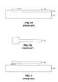
- FIGS. 1A, 1B and 2illustrate a prior art process for forming a MEMS device on a silicon substrate 10 .
- a sacrificial layer 12(conventionally silicon dioxide) is formed over the substrate 10 .
- the MEMS deviceis formed in an overlying structural layer 14 (conventionally polysilicon).
- the structural layer 14is masked, patterned, and etched to produce an elongated member 15 , as illustrated in the top view of FIG. 1B . Any of the known dry or wet etching processes can be employed to form the elongated member 15 from the structural layer 14 .
- the waferthen undergoes a wet etch to remove a significant portion of the sacrificial layer 12 , freeing the elongated member 15 to form a cantilevered beam 16 , as illustrated in FIG. 2 .
- the waferis removed from the etch bath before the entire sacrificial layer 12 is etched away, such that a region 12 A remains as support for the cantilevered beam 16 .
- the removal of a portion of the sacrificial layer 12decouples the elongated member 15 from the substrate 10 , allowing the cantilevered portion of the beam 16 to move relative to the substrate 10 .
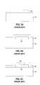
- MEMS devicescomprising partially enclosed chambers can also be fabricated on the surface of the substrate 10 , as illustrated in FIGS. 3A , B, C and D.
- a sacrificial layeris deposited over the substrate 10 and etched to form a sacrificial mesa 20 that defines a volume for the MEMS chamber. See FIG. 3A .
- a polysilicon layer 22is deposited over the substrate 10 and the mesa 20 as illustrated in FIG. 3B .
- a window 24is etched (conventionally by dry reactive ion etching) through the polysilicon layer 22 . See FIG. 3C .
- the waferis then immersed in a wet etch solution, removing the mesa 20 and leaving a windowed chamber 26 .
- etch material selectivity issuescan limit the materials of MEMS structures and integrated circuit devices, as known etch chemistries may not exhibit sufficient selectivities for preferred candidate materials.
- Providing etchant access to sacrificial layerscan also be problematic as etch contact with the sacrificial layer requires access through a suitably sized opening or along an edge of the substrate.
- a process for selectively etching a material layer formed in a structureis described.
- a fluorine-based plasmais formed and the structure temperature is maintained at greater than about 100° C.
- the material layeris etched by exposure to the fluorine-based plasma through an opening extending from a surface of the structure to the material layer.
- a structurecomprising a plurality of material layers in stacked relation comprising a first material layer, a sacrificial layer and a second material.
- An opening in the first material layerextends to the sacrificial layer.
- An etchant introduced into the openingremoves at least a portion of the sacrificial layer.
- FIGS. 1A, 1B and 2illustrate a prior art MEMS structure
- FIGS. 3A-3Dillustrate a prior art MEMS structure during sequential processing steps
- FIGS. 4-7illustrate material substrates during sequential processing steps according to the teachings of the present invention
- FIGS. 8A-8Dillustrate the formation of a reentrant feature according to the teachings of the present invention
- FIGS. 9A-9Cillustrate the formation of a lever arm according to the teachings of the present invention.
- FIG. 10illustrates a plasma-etching chamber for use in accordance with the teachings of the present invention
- FIGS. 11A and 11Billustrate plan and side views of a micro-mirror substrate
- FIGS. 12A and 12Billustrate plan and side views of a micro-mirror formed according to the teachings of the present invention.
- FIG. 4illustrates a layered structure 50 exemplary of a structure that is suitable for use in forming integrated circuit devices or MEMS devices.
- the structure 50comprises, in stacked relation, a substrate 52 , an aluminum layer 54 , a sacrificial titanium nitride layer 56 , a silicon dioxide layer 58 , and a layer 60 formed from any one of several different material types, including silicon (in single crystal, amorphous, and polycrystalline form), silicon dioxide, silicon nitride and aluminum.
- the structure 50further comprises a plurality of vias 61 .
- a viaconventionally comprises a vertical opening or window having a generally circular or rectangular cross-section sized in accordance with its intended function, e.g., providing access to an underlying layer during an etch process or filled with a conductive material to provide a conductive interconnect structure between interconnect layers of an integrated circuit.
- the structure 50is exposed to plasma etchant of nitrogen trifluoride (NF3) at a low pressure (i.e., sub-atmospheric), in a range from about 500 mT to about 50,000 mT.
- NF3nitrogen trifluoride
- the pressurecan be varied to affect the results achievable according to the present invention.
- a surface of the structure 50is maintained at a temperature greater than about 100° C., with a preferred temperature of about 140° C.
- the titanium nitride layer 56is laterally etched through the vias 61 , forming voids 62 as illustrated in FIG. 5 .
- the exposure durationdetermines the amount of material removed and thus the lateral extent of the voids 62 .
- FIG. 5illustrates several voids 62 within the structure 50 , indicating that the process according to the present invention is consistent and repeatable.
- sub-micron sacrificial layerssuch as the titanium nitride layer 56
- the titanium nitride layer 56is about 550 Angstroms thick.
- substantially horizontal trenches (not shown) in the structure 50provide a flow path for the etchant gas to contact the sacrificial layer.
- Certain complimentary metal-oxide field effect transistor (CMOS) structuresinclude trenches at the edge of the integrated circuit chip as a physical boundary and in certain photolithographic alignment structures. For a MEMS device, such trenches and other large area structures, would be common. Via openings and trenches providing contact to underlying trenches, allowing the formation of complex arrays of buried trenches, which are especially advantageous for MEMS devices used for chemical and biological applications and for sensors.
- the titanium nitride layer 56is completely removed, permitting the upper structure, including the silicon dioxide layer 58 and the material layer 60 , to flex upwardly to increase the vertical dimension of the void 62 .
- the layer 56is retained while layers 56 A and 56 B are removed, permitting the layer 56 to move between the layers 54 and 58 .
- the teachings of the inventionare adaptable to remove material layers formed from elemental titanium and other titanium compounds and alloys.
- the process according to the present inventionis also relatively highly material selective in that titanium-based layers can be removed without affecting adjacent aluminum, tungsten, silicon dioxide, silicon nitride and silicon (single crystal, amorphous, and polysilicon) material layers.
- the teachings of the present inventioncan also be applied to an exemplary process for fabricating MEMS structures.
- a titanium-based materialserves as the sacrificial layer.
- the underlying material layercomprises silicon (e.g., silicon nitride or silicon dioxide) and the overlying layer comprises aluminum.
- the sacrificial layercan be removed without adversely impacting the overlying or underlying layers. Since the present invention utilizes a gaseous etch process, it allows for the formation of more delicate and smaller dimension features that might be damaged or removed by a less selective wet etch process.
- the inventioncan be employed to remove the sacrificial layer 12 in FIG. 1A .
- the sacrificial layer 12comprises titanium nitride, elemental titanium or another titanium alloy.
- the materials of the cantilevered beam 16 and the substrate 10may comprise aluminum, silicon dioxide, silicon nitride, tungsten or silicon (single crystal, amorphous, or polysilicon).
- the material selectivity properties of the present inventionallow the use (and etching) of materials not heretofore usable in combination due to the lack of appropriate material selectivity in the etch process.
- a titanium nitride or titanium filmcan be etched without destroying adjacent layers comprised of aluminum, silicon dioxide, silicon nitride, tungsten or silicon (single crystal, amorphous, or polysilicon).
- the aspect ratio of a via or openingis defined as the ratio of the structure height or thickness to the structure diameter or width.
- Known difficultiescan be encountered when attempting to etch underlying layers through high aspect ratio openings, as there may be insufficient contact between the etchant in the high aspect ratio opening and the material layer to be removed.
- the process of the present inventioncan be successfully employed to etch material layers through high aspect ratio openings as the etch gas can penetrate into such openings due to the longer mean free path of the reactive ions in the low pressure nitrogen trifluoride (NF3) etch gas, as compared to the mean free path of other etch gasses. Aspect ratios or greater than about 50 are easily accommodated with the teachings of the present invention.
- the process according to the present inventioncan also be employed to remove sacrificial layers not necessarily exposed through a structural opening (such as a void, trench or via, such as the vias 61 of FIGS. 4 and 5 ).
- the etchantcontacts the sacrificial layer at an exposed edge of the sacrificial layer. See FIG. 6 where a region 70 of the layer 56 is removed when the plasma contacts the layer 56 along an edge 68 of a structure 71 .
- the etch durationcan be extended to completely remove the titanium nitride layer 56 .
- the resulting voidpermits the mechanical separation of the aluminum layer 54 from the silicon dioxide layer 58 .
- a capacitorcan be created by the formation of conductive material on the two opposing void surfaces, where the separation distance is controlled to determine the capacitance value.
- MEMS micromachine elementssuch as gears, require decoupling between two layers to permit structure movement.
- C x F y and C x H y F z chemistriescan be adapted for use according to the teachings of the present invention.
- Contact resistance in an integrated circuit deviceis a measure of the resistance between an interconnect structure, such as a conductive via, and a doped region of the substrate. Since a typical integrated circuit includes a substantial number of such contacts, the total interconnect resistance can be significantly reduced by reducing the resistance of each contact. According to the prior art, the contact resistance is reduced by increasing the contact surface area, i.e., enlarging the conductive via cross-section. But increasing the via size disadvantageously increases the overall device size. According to one embodiment of the present invention a reduced contact resistance can be formed in an integrated circuit device as follows.
- a via 72is formed over a doped region 74 of a substrate 75 .
- the via 72is filled with conductive material to form a conductive via in electrical contact with the doped region 74 .
- An upper surface of the conductive viais connected to other interconnect structures of the integrated circuit.
- the contact resistance between the conductive via and the doped region 74is determined in part by the contact surface area.
- a region of a sacrificial layer 77is removed by etching as described above. If the sacrificial layer 77 is also present in other regions of the substrate 77 , these regions can be protected from exposure to the etchants.
- the etchantcontacts the sacrificial layer 77 through the via 72 or along an edge 79 to remove the layer 77 as shown in FIG. 7B .
- a conductive interface 80(see FIG. 7C ) is formed within an opening created by removal of the sacrificial layer 77 . Since the conductive interface 80 presents a larger contact area with the doped region 74 than the contact area of a conductive via, the contact resistance is lowered without increasing the device size.
- the via 72is then filled with conductive material (such as tungsten) according to known process steps.
- teachings of the present inventioncan be employed to form a re-entrant feature profile for a microelectronics or MEMS device.
- a structure 100is illustrated in FIG. 8A , including a silicon dioxide layer 101 , a titanium-nitride layer 102 , titanium-nitride segments 104 A and 104 B, aluminum interconnect layers 105 A and 105 B, titanium layers 106 A and 106 B, and a silicon dioxide layer 108 .
- a via 112formed by conventional processing, extends from an upper surface 114 of the silicon dioxide layer 108 to the titanium-nitride layer 102 as illustrated in FIG. 8B .
- the teachings of the present inventionare employed to etch regions 116 of the titanium-nitride layers 102 and 106 , forming a reentrant feature 118 . See FIG. 8C .
- the etch durationdetermines the amount of titanium-nitride removed and thus the reentrant feature size.
- Conductive materialcan be deposited within the reentrant feature 118 to form one or more capacitors.
- silicon dioxide layers 108 A and 108 Bcan operate as capacitive dielectric materials, each operative with plates formed in regions 118 A and 118 B, where a portion of the titanium-nitride layers 106 A and 106 B has been removed as described above. See FIG. 8D .
- a second plate for each capacitoris formed in regions 119 A and 119 B, overlying the silicon dioxide layers 108 A and 108 B, respectively.
- a second pair of capacitorsare formed by conductive material disposed in regions 119 C and 119 D underlying the silicon dioxide layer 101 , which serves as the capacitive dielectric material.
- Opposing plates for the second pair of capacitorsare formed in regions 118 C and 118 D, where portions of the titanium-nitride layer 102 have been removed.
- the aluminum interconnect layers 105 A and 105 Bserve as capacitor plates with a dielectric material therebetween in a region 118 E.
- One suitable dielectric materialcomprises air.
- a dielectric materialcan be formed in the region 118 E to serve as a capacitive dielectric.
- a capacitance of the last mentioned configurationis relatively small and can thus be used to tune other capacitors formed on the substrate by adding or subtracting a small capacitance therefrom.
- Capacitors so formedcan also operate as sensing devices within microelectromechanical devices.
- FIG. 8Dillustrates a vertical cross-sectional view, the various conductive and dielectric layers of the capacitor can extend into the plane of the paper, including extending in a serpentine or meandering configuration, to affect the physical dimensions, configuration and capacitance of the capacitor
- a lever arm of an accelerometercan be formed in an isolated cavity.
- a structure 120is illustrated in FIG. 9A , including a silicon dioxide layer 121 , a titanium-nitride layer 122 , titanium-nitride segments 124 A and 124 B, aluminum layers 125 A and 125 B, titanium layers 126 A and 126 B, and a silicon dioxide layer 128 .
- a via 132formed by conventional processing, extends from an upper surface 134 of the silicon dioxide layer 128 to the titanium-nitride layer 122 as illustrated in FIG. 9B .
- the teachings of the present inventionare employed to etch regions 136 of the titanium-nitride layers 122 , 126 A and 126 B, forming a lever arm 137 of FIG. 9C .
- the etch durationdetermines the amount of titanium-nitride removed and thus the free length of the lever arm 137 .
- FIG. 10illustrates a plasma chamber 140 , suitable for use according to the present invention, having an inlet 142 for receiving nitrogen trifluoride from a gaseous supply.
- a power supply 144provides radio frequency energy to an electrode 146 for creating a plasma of nitrogen trifluoride within the chamber 140 .
- the plasmais formed the nitrogen and fluorine disassociate.
- the plasma chamber 140is maintained at a subatomic pressure range from about 500 mT to about 50,000 mT.
- an inert carrier gassuch as helium or argon, can be added to the gas flow through the inlet 142 .
- the plasmais supplied to a reaction chamber 148 (maintained at a pressure from about 500 to about 3500 mT) where one or more wafers 150 are disposed on a platform 152 .
- the plasma temperature upon entering the reaction chamberis in the range from about 100° C. to about 200° C.
- the wafers 150are also maintained at a temperature between about 100° C. to about 200° C.
- the plasmaselectively etches titanium or titanium-nitride sacrificial films, such as the titanium-nitride layer 56 of FIG. 4 , as described above.
- the process according to the present inventioncan be employed in various embodiments to remove a sacrificial layer of titanium, titanium-nitride or another titanium compound or alloy from between: two silicon layers (e.g., polysilicon, amorphous silicon and single-crystal silicon, including silicon compounds), two silicon dioxide layers, two silicon nitride layers, two aluminum layers (including elemental aluminum and aluminum compounds and alloys), two tungsten layers or any combination of these materials.
- the etching process according to the present inventionis selective to remove only the titanium-based layer, leaving the other material layers intact. Further, the process is effective to etch material through openings, including high-aspect ratio openings.
- Exemplary etch ratios for the various materials referred to herein based on known etch chemistriesinclude: titanium:silicon: greater than about 10:1; titanium:silicon dioxide: greater than about 10:1; titanium nitride:aluminum: greater than about 50:1; titanium:silicon nitride: greater than about 10:1.
- the etch selectivity provided by the present inventionreduces the effects of an over etch condition.
- a MEMS structuresuch as the lever arm 137 illustrated in FIG. 9C
- a MEMS structurecan be formed of aluminum on a substrate carrying integrated circuit active devices. Since the aluminum can be deposited on the substrate at temperatures below about 400° C., the previously-formed integrated circuit devices are not adversely affected during the aluminum deposition process.
- one or more sacrificial layersare deposited and patterned after formation of the active circuit devices in the substrate material.
- the aluminumis deposited and the techniques of the present invention are employed to remove the sacrificial layers disposed between the aluminum and the underlying substrate, forming a MEMS structure.
- the process of etching the sacrificial layer or layerscan be accomplished, as described above, through relatively small aspect ratio openings, through trenches in the substrate or by etch exposure of the sacrificial layer at an edge surface of the substrate.
- the present inventionprovides an enabling technology for forming MEMS devices from aluminum on the same substrate as integrated circuit devices.
- FIGS. 11A and 11Billustrate a top and side view, respectively, of a micro-mirror 160 comprising a mirror material 162 disposed overlying a titanium-nitride material layer 164 and a substrate 166 .
- the micro-mirror 160is exposed to a titanium-nitride etch process according to the teachings of the present invention through an opening 167 in the substrate 166 to remove the titanium-nitride layer 164 .
- the resulting structureis illustrated in FIGS. 12A and 12B .
- a gap 168 formed by removal of the titanium-nitride layer 164permits a movable or pivotable portion 170 of the mirror material 162 to controllably rotate or pivot about arms 171 according to techniques known in the art.
- the implementation of the etching process of the present invention at a relatively low temperatureenables the formation of MEMS structures proximate integrated circuit devices, in that the low temperature etching process does not impact the previously formed integrated circuit devices.
- Temperature sensitive materials that could be damaged by high temperature steps in prior art MEMS processescan be employed to form MEMS devices according to the teachings of the present invention since high temperature steps can be avoided.
Landscapes
- Engineering & Computer Science (AREA)
- Physics & Mathematics (AREA)
- Chemical & Material Sciences (AREA)
- Microelectronics & Electronic Packaging (AREA)
- Manufacturing & Machinery (AREA)
- Metallurgy (AREA)
- Organic Chemistry (AREA)
- Geometry (AREA)
- Mechanical Engineering (AREA)
- Materials Engineering (AREA)
- Plasma & Fusion (AREA)
- Condensed Matter Physics & Semiconductors (AREA)
- General Physics & Mathematics (AREA)
- Computer Hardware Design (AREA)
- Power Engineering (AREA)
- Micromachines (AREA)
- ing And Chemical Polishing (AREA)
- Drying Of Semiconductors (AREA)
Abstract
Description
- The present invention relates generally to etching material layers in a semiconductor or microelectromechanical systems device, and more specifically to a process for etching titanium-based layers (including titanium-nitride) in such devices.
- Microelectromechanical (MEM) systems comprise integrated micro devices, such as mechanical components, formed on a substrate material. The systems, which are fabricated using integrated circuit batch processing techniques, range in size from nanometers to millimeters. MEMS devices are operable individually to sense, control, and actuate on a micro scale, or can function in arrays to generate effects on a macro scale. Current MEMS device applications include accelerometers, inertial and angular sensors, pressure sensors, chemical and flow sensors, micro-optics devices, optical scanners, fluid flow devices, chemical sensing and chemical delivery systems, and biological sensors. In one application, MEMS devices are formed with micro-channels in a substrate and layered devices for use in chemical and biological analysis according to the channel dimensions.
- MEMS devices further comprise electronic components in the form of integrated circuit devices formed on the same silicon chip as a mechanical MEMS device. Advantageously, MEMS devices reduce the size and weight of mechanical and electromechanical systems when compared with conventional mechanical systems.
- Fabrication of MEMS devices employs many of the same processing steps as the fabrication of integrated circuits. In particular, the formation of a MEMS device involves depositing and patterning thin films on a substrate surface, such as a silicon wafer surface, to produce complex microstructures. Common thin film materials (applied with a thickness on the order of micrometers or less) include silicon dioxide, silicon nitride, polycrystalline silicon (poly), amorphous silicon, aluminum, refractory metals and suicides. To provide mechanical movement for MEMS devices, it is necessary to decouple the structural elements to form a gap between the moving elements. Thus a selective etch process is used to form the gap by removing material without affecting the operative structures.
- After depositing a material layer, photolithographic masking, patterning and etching steps are employed to remove the unwanted material. Generally, etch processes fall into two categories, wet etching and dry etching. According to a wet etch chemistry, the structure is immersed in or exposed to a liquid chemical bath containing an etchant solution, for example a buffered HF solution, until the unwanted material has been removed. For more effective wet etching, the wafer is mechanically or ultrasonically agitated during immersion in the etchant bath. Wet etching requires contact between the material layer to be removed and the etchant solution. The contact occurs along one or more exposed surfaces or edges of the material layer. If the surface or edge is not sufficiently accessible to the etchant, an opening may be formed in the overlying layers, extending down to the material layer, providing a path along which the etchant may flow to contact and etch the material. Following completion of the wet etch process the wafer is rinsed and spun dry.
- Generally, etchants are subdivided into two broad categories, referred to as isotropic etchants and anisotropic etchants. Wet isotropic etchants, which are available for silicon dioxide, nitrides, aluminum, polysilicon, gold, and silicon, attack the material at the substantially the same rate in all directions, removing material vertically and horizontally under the photolithographic etch mask. In some applications, significant undesirable horizontal etching, referred to as undercutting, can occur during the isotropic etch process. Anisotropic etchants attack the material layers at different rates in different directions and may be applied to achieve greater control or geometric selectivity during the material removal process.
- In addition to geometric selectivity, etchants are also material selective, that is, a specific etch chemistry etches different materials at different etch rates. For example, hydrofluoric acid (HF) etches silicon dioxide without significantly attacking silicon. However, wet etchants that are effective in removing silicon dioxide and silicon generally do not exhibit satisfactory selectivity to preserve metals, such as aluminum. Generally, in the fabrication of integrated circuit devices and MEMS structures, it has been difficult to remove silicon or silicon dioxide without substantially eroding adjacent aluminum or other metallized features.
- Dry etch processes typically use a gas as the primary etchant without accompanying wet chemicals or rinses. Some dry etch processes are less aggressive than wet processes, allowing the formation of smaller and more delicate structures on the wafer surface due to the decreased risk of structure damage.
- Downstream plasma etching, one type of dry etching, applies plasma energy to a gas, initiating a chemical reaction that performs the material etching. A plasma etching system comprises a chamber, vacuum system, gas supply, power supply and microwave source (or another suitable radio frequency signal source). Wafers are loaded into the chamber and positioned on a grounded platen disposed below a microwave-energized electrode. The chamber pressure is reduced to establish a vacuum and a gas (or a combination of gasses) is introduced into a microwave plasma tube. For example, when etching silicon dioxide, CF4 is mixed with oxygen, which serves as a passivating agent. As the gas mixture flows into the chamber, the microwave source supplies energy to the plasma tube, dissociating the CF4 into a cloud of fluorine and carbon radicals. In this state, the fluorine attacks and etches the silicon dioxide, converting it to volatile components that are removed from the chamber by the vacuum system.
- In addition to material and directional selectivity mentioned above, a limitation common to both wet and dry etch techniques is the inability to compensate for etch rate variations due to dimension and size variations, i.e., variations in line density, critical dimension, open area percentage and layer thickness, in the structure to be etched. For example, a substrate area with large critical dimensions generally experiences a higher etch rate than a region with small critical dimensions. In general, areas with higher etch rates will etch through a material layer, and begin to etch an underlying layer in advance of regions having slower etch rates. To overcome this difficulty, the duration of an etch process is typically determined by the etch rate of the region experiencing the slowest etch rate, thereby achieving complete removal of the material to be etched. Also, non-critical features are compensated in the physical layout to account for the etch rate variations based on feature size to achieve the desired final feature size.
FIGS. 1A, 1B and2 illustrate a prior art process for forming a MEMS device on asilicon substrate 10. As shown inFIG. 1A , a sacrificial layer12 (conventionally silicon dioxide) is formed over thesubstrate 10. The MEMS device is formed in an overlying structural layer14 (conventionally polysilicon). In this example, thestructural layer 14 is masked, patterned, and etched to produce anelongated member 15, as illustrated in the top view ofFIG. 1B . Any of the known dry or wet etching processes can be employed to form theelongated member 15 from thestructural layer 14. The wafer then undergoes a wet etch to remove a significant portion of thesacrificial layer 12, freeing theelongated member 15 to form a cantilevered beam16, as illustrated inFIG. 2 . The wafer is removed from the etch bath before the entiresacrificial layer 12 is etched away, such that aregion 12A remains as support for the cantilevered beam16. Thus the removal of a portion of thesacrificial layer 12 decouples theelongated member 15 from thesubstrate 10, allowing the cantilevered portion of the beam16 to move relative to thesubstrate 10.- MEMS devices comprising partially enclosed chambers can also be fabricated on the surface of the
substrate 10, as illustrated inFIGS. 3A , B, C and D. A sacrificial layer is deposited over thesubstrate 10 and etched to form asacrificial mesa 20 that defines a volume for the MEMS chamber. SeeFIG. 3A . Apolysilicon layer 22 is deposited over thesubstrate 10 and themesa 20 as illustrated inFIG. 3B . Next awindow 24 is etched (conventionally by dry reactive ion etching) through thepolysilicon layer 22. SeeFIG. 3C . The wafer is then immersed in a wet etch solution, removing themesa 20 and leaving awindowed chamber 26. - According to the prior art, etch material selectivity issues can limit the materials of MEMS structures and integrated circuit devices, as known etch chemistries may not exhibit sufficient selectivities for preferred candidate materials. Providing etchant access to sacrificial layers can also be problematic as etch contact with the sacrificial layer requires access through a suitably sized opening or along an edge of the substrate.
- A process for selectively etching a material layer formed in a structure is described. A fluorine-based plasma is formed and the structure temperature is maintained at greater than about 100° C. The material layer is etched by exposure to the fluorine-based plasma through an opening extending from a surface of the structure to the material layer.
- A structure comprising a plurality of material layers in stacked relation comprising a first material layer, a sacrificial layer and a second material. An opening in the first material layer extends to the sacrificial layer. An etchant introduced into the opening removes at least a portion of the sacrificial layer.
- The foregoing and other features of the invention will be apparent from the following more particular description of the invention, as illustrated in the accompanying drawings, in which like reference characters refer to the same parts throughout the different figures. The drawings are not necessarily to scale, emphasis instead being placed upon illustrating the principles of the invention.
FIGS. 1A, 1B and2 illustrate a prior art MEMS structure;FIGS. 3A-3D illustrate a prior art MEMS structure during sequential processing steps;FIGS. 4-7 illustrate material substrates during sequential processing steps according to the teachings of the present invention;FIGS. 8A-8D illustrate the formation of a reentrant feature according to the teachings of the present invention;FIGS. 9A-9C illustrate the formation of a lever arm according to the teachings of the present invention;FIG. 10 illustrates a plasma-etching chamber for use in accordance with the teachings of the present invention;FIGS. 11A and 11B illustrate plan and side views of a micro-mirror substrate; andFIGS. 12A and 12B illustrate plan and side views of a micro-mirror formed according to the teachings of the present invention.- Before describing in detail the particular etch process in accordance with the present invention, it should be observed that the present invention resides primarily in a novel combination of elements and process steps. Accordingly, the elements have been represented by conventional elements in the drawings, showing only those specific details that are pertinent to the present invention so as not to obscure the disclosure with structural details that will be readily apparent to those skilled in the art having the benefit of the description herein.
FIG. 4 illustrates alayered structure 50 exemplary of a structure that is suitable for use in forming integrated circuit devices or MEMS devices. Thestructure 50 comprises, in stacked relation, asubstrate 52, analuminum layer 54, a sacrificialtitanium nitride layer 56, asilicon dioxide layer 58, and alayer 60 formed from any one of several different material types, including silicon (in single crystal, amorphous, and polycrystalline form), silicon dioxide, silicon nitride and aluminum. Thestructure 50 further comprises a plurality ofvias 61. As is known in the art, a via conventionally comprises a vertical opening or window having a generally circular or rectangular cross-section sized in accordance with its intended function, e.g., providing access to an underlying layer during an etch process or filled with a conductive material to provide a conductive interconnect structure between interconnect layers of an integrated circuit.- According to the teachings of the present invention, the
structure 50 is exposed to plasma etchant of nitrogen trifluoride (NF3) at a low pressure (i.e., sub-atmospheric), in a range from about 500 mT to about 50,000 mT. The pressure can be varied to affect the results achievable according to the present invention. In one embodiment, a surface of thestructure 50 is maintained at a temperature greater than about 100° C., with a preferred temperature of about 140° C. During the etching process thetitanium nitride layer 56 is laterally etched through thevias 61, formingvoids 62 as illustrated inFIG. 5 . The exposure duration determines the amount of material removed and thus the lateral extent of thevoids 62. Raising the exposure time etches more of thetitanium nitride layer 56 and extends thevoids 62. A sufficiently long exposure would cause the etchant to completely remove thetitanium nitride layer 56.FIG. 5 illustratesseveral voids 62 within thestructure 50, indicating that the process according to the present invention is consistent and repeatable. - As a result of the gaseous, low-pressure etch conditions of the present invention, sub-micron sacrificial layers, such as the
titanium nitride layer 56, can be effectively removed as the etchant gas contacts the sacrificial layer through thevias 61. In oneexemplary structure 50, thetitanium nitride layer 56 is about 550 Angstroms thick. - In another embodiment, substantially horizontal trenches (not shown) in the
structure 50 provide a flow path for the etchant gas to contact the sacrificial layer. Certain complimentary metal-oxide field effect transistor (CMOS) structures include trenches at the edge of the integrated circuit chip as a physical boundary and in certain photolithographic alignment structures. For a MEMS device, such trenches and other large area structures, would be common. Via openings and trenches providing contact to underlying trenches, allowing the formation of complex arrays of buried trenches, which are especially advantageous for MEMS devices used for chemical and biological applications and for sensors. - In another embodiment, the
titanium nitride layer 56 is completely removed, permitting the upper structure, including thesilicon dioxide layer 58 and thematerial layer 60, to flex upwardly to increase the vertical dimension of the void62. - In yet another embodiment, the
layer 56 is retained whilelayers layer 56 to move between thelayers - Although described above with respect to a titanium-nitride sacrificial layer, in another embodiment the teachings of the invention are adaptable to remove material layers formed from elemental titanium and other titanium compounds and alloys. The process according to the present invention is also relatively highly material selective in that titanium-based layers can be removed without affecting adjacent aluminum, tungsten, silicon dioxide, silicon nitride and silicon (single crystal, amorphous, and polysilicon) material layers. The teachings of the present invention can also be applied to an exemplary process for fabricating MEMS structures. A titanium-based material serves as the sacrificial layer. The underlying material layer comprises silicon (e.g., silicon nitride or silicon dioxide) and the overlying layer comprises aluminum. Employing a process according to the teachings of the present invention, the sacrificial layer can be removed without adversely impacting the overlying or underlying layers. Since the present invention utilizes a gaseous etch process, it allows for the formation of more delicate and smaller dimension features that might be damaged or removed by a less selective wet etch process.
- The invention can be employed to remove the
sacrificial layer 12 inFIG. 1A . In this application thesacrificial layer 12 comprises titanium nitride, elemental titanium or another titanium alloy. The materials of the cantilevered beam16 and thesubstrate 10 may comprise aluminum, silicon dioxide, silicon nitride, tungsten or silicon (single crystal, amorphous, or polysilicon). Thus in the manufacture of MEMS structures, the material selectivity properties of the present invention allow the use (and etching) of materials not heretofore usable in combination due to the lack of appropriate material selectivity in the etch process. - The material selectivity characteristics of the present invention also allow the use of such materials in the fabrication of integrated circuit devices. For example, a titanium nitride or titanium film can be etched without destroying adjacent layers comprised of aluminum, silicon dioxide, silicon nitride, tungsten or silicon (single crystal, amorphous, or polysilicon).
- The aspect ratio of a via or opening is defined as the ratio of the structure height or thickness to the structure diameter or width. Known difficulties can be encountered when attempting to etch underlying layers through high aspect ratio openings, as there may be insufficient contact between the etchant in the high aspect ratio opening and the material layer to be removed. The process of the present invention can be successfully employed to etch material layers through high aspect ratio openings as the etch gas can penetrate into such openings due to the longer mean free path of the reactive ions in the low pressure nitrogen trifluoride (NF3) etch gas, as compared to the mean free path of other etch gasses. Aspect ratios or greater than about 50 are easily accommodated with the teachings of the present invention.
- The process according to the present invention can also be employed to remove sacrificial layers not necessarily exposed through a structural opening (such as a void, trench or via, such as the
vias 61 ofFIGS. 4 and 5 ). In such an application, the etchant contacts the sacrificial layer at an exposed edge of the sacrificial layer. SeeFIG. 6 where aregion 70 of thelayer 56 is removed when the plasma contacts thelayer 56 along anedge 68 of astructure 71. - The etch duration can be extended to completely remove the
titanium nitride layer 56. The resulting void permits the mechanical separation of thealuminum layer 54 from thesilicon dioxide layer 58. Thus these two layers are completely decoupled, a process that can be advantageously employed in the formation of MEMS devices and structures and also in the fabrication of semiconductor devices. In the latter application, a capacitor can be created by the formation of conductive material on the two opposing void surfaces, where the separation distance is controlled to determine the capacitance value. In the former application, MEMS micromachine elements, such as gears, require decoupling between two layers to permit structure movement. - According to other embodiments of the present invention other fluorine-containing chemistries can be used to etch the sacrificial layer. For example, CxFyand CxHyFzchemistries can be adapted for use according to the teachings of the present invention.
- Contact resistance in an integrated circuit device is a measure of the resistance between an interconnect structure, such as a conductive via, and a doped region of the substrate. Since a typical integrated circuit includes a substantial number of such contacts, the total interconnect resistance can be significantly reduced by reducing the resistance of each contact. According to the prior art, the contact resistance is reduced by increasing the contact surface area, i.e., enlarging the conductive via cross-section. But increasing the via size disadvantageously increases the overall device size. According to one embodiment of the present invention a reduced contact resistance can be formed in an integrated circuit device as follows.
- As illustrated in
FIG. 7A , a via72 is formed over a dopedregion 74 of asubstrate 75. According to the prior art, the via72 is filled with conductive material to form a conductive via in electrical contact with the dopedregion 74. An upper surface of the conductive via is connected to other interconnect structures of the integrated circuit. The contact resistance between the conductive via and the dopedregion 74 is determined in part by the contact surface area. - According to the teachings of the present invention, after formation of the via72 a region of a
sacrificial layer 77 is removed by etching as described above. If thesacrificial layer 77 is also present in other regions of thesubstrate 77, these regions can be protected from exposure to the etchants. The etchant contacts thesacrificial layer 77 through the via72 or along anedge 79 to remove thelayer 77 as shown inFIG. 7B . A conductive interface80 (seeFIG. 7C ) is formed within an opening created by removal of thesacrificial layer 77. Since theconductive interface 80 presents a larger contact area with the dopedregion 74 than the contact area of a conductive via, the contact resistance is lowered without increasing the device size. The via72 is then filled with conductive material (such as tungsten) according to known process steps. - In yet another embodiment, the teachings of the present invention can be employed to form a re-entrant feature profile for a microelectronics or MEMS device. A
structure 100 is illustrated inFIG. 8A , including asilicon dioxide layer 101, a titanium-nitride layer 102, titanium-nitride segments aluminum interconnect layers titanium layers silicon dioxide layer 108. - A via112, formed by conventional processing, extends from an
upper surface 114 of thesilicon dioxide layer 108 to the titanium-nitride layer 102 as illustrated inFIG. 8B . The teachings of the present invention are employed to etchregions 116 of the titanium-nitride layers 102 and106, forming areentrant feature 118. SeeFIG. 8C . The etch duration determines the amount of titanium-nitride removed and thus the reentrant feature size. - Conductive material can be deposited within the
reentrant feature 118 to form one or more capacitors. For example,silicon dioxide layers regions nitride layers FIG. 8D . A second plate for each capacitor is formed inregions silicon dioxide layers regions silicon dioxide layer 101, which serves as the capacitive dielectric material. Opposing plates for the second pair of capacitors are formed inregions nitride layer 102 have been removed. In yet another capacitor configuration, thealuminum interconnect layers region 118E. One suitable dielectric material comprises air. In other embodiments, a dielectric material can be formed in theregion 118E to serve as a capacitive dielectric. The capacitors described above provide a range of capacitance values depending on the characteristics of the various elements, including the dielectric material and the plate spacing. Generally, a capacitance of the last mentioned configuration is relatively small and can thus be used to tune other capacitors formed on the substrate by adding or subtracting a small capacitance therefrom. Capacitors so formed can also operate as sensing devices within microelectromechanical devices. Further, recognizing thatFIG. 8D illustrates a vertical cross-sectional view, the various conductive and dielectric layers of the capacitor can extend into the plane of the paper, including extending in a serpentine or meandering configuration, to affect the physical dimensions, configuration and capacitance of the capacitor - In a MEMS application, a lever arm of an accelerometer can be formed in an isolated cavity. A
structure 120 is illustrated inFIG. 9A , including asilicon dioxide layer 121, a titanium-nitride layer 122, titanium-nitride segments aluminum layers titanium layers silicon dioxide layer 128. Although several of the inventive embodiments have been described with reference to material layers such as those illustrated inFIG. 9A , those skilled in the art recognize that the teachings of the present invention can be employed with other material layers having configurations and orientations other than those illustrated herein. - A via132, formed by conventional processing, extends from an
upper surface 134 of thesilicon dioxide layer 128 to the titanium-nitride layer 122 as illustrated inFIG. 9B . The teachings of the present invention are employed to etchregions 136 of the titanium-nitride layers lever arm 137 ofFIG. 9C . The etch duration determines the amount of titanium-nitride removed and thus the free length of thelever arm 137. FIG. 10 illustrates aplasma chamber 140, suitable for use according to the present invention, having aninlet 142 for receiving nitrogen trifluoride from a gaseous supply. Apower supply 144 provides radio frequency energy to anelectrode 146 for creating a plasma of nitrogen trifluoride within thechamber 140. When the plasma is formed the nitrogen and fluorine disassociate. Theplasma chamber 140 is maintained at a subatomic pressure range from about 500 mT to about 50,000 mT. In an alternative embodiment an inert carrier gas, such as helium or argon, can be added to the gas flow through theinlet 142. The plasma is supplied to a reaction chamber148 (maintained at a pressure from about 500 to about 3500 mT) where one ormore wafers 150 are disposed on aplatform 152. The plasma temperature upon entering the reaction chamber is in the range from about 100° C. to about 200° C. Thewafers 150 are also maintained at a temperature between about 100° C. to about 200° C. The plasma selectively etches titanium or titanium-nitride sacrificial films, such as the titanium-nitride layer 56 ofFIG. 4 , as described above.- Although described above with respect to titanium-nitride layers, the process according to the present invention can be employed in various embodiments to remove a sacrificial layer of titanium, titanium-nitride or another titanium compound or alloy from between: two silicon layers (e.g., polysilicon, amorphous silicon and single-crystal silicon, including silicon compounds), two silicon dioxide layers, two silicon nitride layers, two aluminum layers (including elemental aluminum and aluminum compounds and alloys), two tungsten layers or any combination of these materials. The etching process according to the present invention is selective to remove only the titanium-based layer, leaving the other material layers intact. Further, the process is effective to etch material through openings, including high-aspect ratio openings.
- Exemplary etch ratios for the various materials referred to herein based on known etch chemistries include: titanium:silicon: greater than about 10:1; titanium:silicon dioxide: greater than about 10:1; titanium nitride:aluminum: greater than about 50:1; titanium:silicon nitride: greater than about 10:1. The etch selectivity provided by the present invention reduces the effects of an over etch condition.
- In one application of the present invention, a MEMS structure, such as the
lever arm 137 illustrated inFIG. 9C , can be formed of aluminum on a substrate carrying integrated circuit active devices. Since the aluminum can be deposited on the substrate at temperatures below about 400° C., the previously-formed integrated circuit devices are not adversely affected during the aluminum deposition process. - To form such a MEMS structure, one or more sacrificial layers are deposited and patterned after formation of the active circuit devices in the substrate material. The aluminum is deposited and the techniques of the present invention are employed to remove the sacrificial layers disposed between the aluminum and the underlying substrate, forming a MEMS structure. The process of etching the sacrificial layer or layers can be accomplished, as described above, through relatively small aspect ratio openings, through trenches in the substrate or by etch exposure of the sacrificial layer at an edge surface of the substrate. Thus the present invention provides an enabling technology for forming MEMS devices from aluminum on the same substrate as integrated circuit devices.
- In another embodiment, micro-mirror structures can be formed on an integrated circuit substrate according to this technique.
FIGS. 11A and 11B illustrate a top and side view, respectively, of a micro-mirror160 comprising amirror material 162 disposed overlying a titanium-nitride material layer 164 and asubstrate 166. The micro-mirror160 is exposed to a titanium-nitride etch process according to the teachings of the present invention through anopening 167 in thesubstrate 166 to remove the titanium-nitride layer 164. The resulting structure is illustrated inFIGS. 12A and 12B . Agap 168 formed by removal of the titanium-nitride layer 164 permits a movable orpivotable portion 170 of themirror material 162 to controllably rotate or pivot aboutarms 171 according to techniques known in the art. - Advantageously, the implementation of the etching process of the present invention at a relatively low temperature enables the formation of MEMS structures proximate integrated circuit devices, in that the low temperature etching process does not impact the previously formed integrated circuit devices. Temperature sensitive materials that could be damaged by high temperature steps in prior art MEMS processes can be employed to form MEMS devices according to the teachings of the present invention since high temperature steps can be avoided.
- A process has been described as useful for etching layers of a substrate. While specific applications and examples of the invention have been illustrated and discussed, the principles disclosed herein provide a basis for practicing the invention in a variety of ways and in a variety of integrated circuit and MEMS structures. Numerous variations are possible within the scope of the invention. The invention is limited only by the claims that follow.
Claims (51)
Priority Applications (6)
| Application Number | Priority Date | Filing Date | Title |
|---|---|---|---|
| US10/675,263US7078337B2 (en) | 2003-09-30 | 2003-09-30 | Selective isotropic etch for titanium-based materials |
| TW093123935ATW200518217A (en) | 2003-09-30 | 2004-08-10 | Selective isotropic etch for titanium-based materials |
| GB0420952AGB2408848A (en) | 2003-09-30 | 2004-09-21 | Selective isotropic etch for titanium-based materials |
| JP2004278932AJP4855665B2 (en) | 2003-09-30 | 2004-09-27 | Selective isotropic etching process of titanium-based materials |
| KR1020040078027AKR101214818B1 (en) | 2003-09-30 | 2004-09-30 | Selective isotropic etch for titanium-based materials |
| US11/368,780US7476951B2 (en) | 2003-09-30 | 2006-03-06 | Selective isotropic etch for titanium-based materials |
Applications Claiming Priority (1)
| Application Number | Priority Date | Filing Date | Title |
|---|---|---|---|
| US10/675,263US7078337B2 (en) | 2003-09-30 | 2003-09-30 | Selective isotropic etch for titanium-based materials |
Related Child Applications (1)
| Application Number | Title | Priority Date | Filing Date |
|---|---|---|---|
| US11/368,780DivisionUS7476951B2 (en) | 2003-09-30 | 2006-03-06 | Selective isotropic etch for titanium-based materials |
Publications (2)
| Publication Number | Publication Date |
|---|---|
| US20050068608A1true US20050068608A1 (en) | 2005-03-31 |
| US7078337B2 US7078337B2 (en) | 2006-07-18 |
Family
ID=33311158
Family Applications (2)
| Application Number | Title | Priority Date | Filing Date |
|---|---|---|---|
| US10/675,263Expired - LifetimeUS7078337B2 (en) | 2003-09-30 | 2003-09-30 | Selective isotropic etch for titanium-based materials |
| US11/368,780Expired - LifetimeUS7476951B2 (en) | 2003-09-30 | 2006-03-06 | Selective isotropic etch for titanium-based materials |
Family Applications After (1)
| Application Number | Title | Priority Date | Filing Date |
|---|---|---|---|
| US11/368,780Expired - LifetimeUS7476951B2 (en) | 2003-09-30 | 2006-03-06 | Selective isotropic etch for titanium-based materials |
Country Status (5)
| Country | Link |
|---|---|
| US (2) | US7078337B2 (en) |
| JP (1) | JP4855665B2 (en) |
| KR (1) | KR101214818B1 (en) |
| GB (1) | GB2408848A (en) |
| TW (1) | TW200518217A (en) |
Cited By (11)
| Publication number | Priority date | Publication date | Assignee | Title |
|---|---|---|---|---|
| US20070145501A1 (en)* | 2003-07-04 | 2007-06-28 | Stmicroelectronics S.R.L. | Semiconductor device having a suspended micro-system |
| US20080029481A1 (en)* | 2006-08-02 | 2008-02-07 | Manish Kothari | Methods for reducing surface charges during the manufacture of microelectromechanical systems devices |
| WO2008084365A3 (en)* | 2007-01-05 | 2008-09-04 | Nxp Bv | Etching with improved control of critical feature dimensions at the bottom of thick layers |
| US20090218312A1 (en)* | 2004-09-27 | 2009-09-03 | Idc, Llc | Method and system for xenon fluoride etching with enhanced efficiency |
| US20090262412A1 (en)* | 2004-09-27 | 2009-10-22 | Idc, Llc | Method of fabricating interferometric devices using lift-off processing techniques |
| US20100015744A1 (en)* | 2005-11-22 | 2010-01-21 | Cavendish Kinetics Ltd. | Micro-Electromechanical Device and Method of Making the Same |
| US20100079847A1 (en)* | 2008-09-30 | 2010-04-01 | Qualcomm Mems Technologies, Inc. | Multi-thickness layers for mems and mask-saving sequence for same |
| US20130050686A1 (en)* | 2011-08-25 | 2013-02-28 | Palo Alto Research Center Incorporated | Gap distributed bragg reflectors |
| US20150056732A1 (en)* | 2013-08-26 | 2015-02-26 | International Business Machines Corporation | Solid state nanopore devices and methods of manufacture |
| US20180086627A1 (en)* | 2015-06-22 | 2018-03-29 | Intel Corporation | Integrating mems structures with interconnects and vias |
| US20190004659A1 (en)* | 2017-06-30 | 2019-01-03 | Shanghai Tianma Micro-electronics Co., Ltd. | Display panel and display device |
Families Citing this family (11)
| Publication number | Priority date | Publication date | Assignee | Title |
|---|---|---|---|---|
| US7417783B2 (en)* | 2004-09-27 | 2008-08-26 | Idc, Llc | Mirror and mirror layer for optical modulator and method |
| US7875484B2 (en)* | 2006-11-20 | 2011-01-25 | Alces Technology, Inc. | Monolithic IC and MEMS microfabrication process |
| US20120057216A1 (en)* | 2007-09-28 | 2012-03-08 | Qualcomm Mems Technologies, Inc. | Multicomponent sacrificial structure |
| US8507385B2 (en)* | 2008-05-05 | 2013-08-13 | Shanghai Lexvu Opto Microelectronics Technology Co., Ltd. | Method for processing a thin film micro device on a substrate |
| US7928577B2 (en)* | 2008-07-16 | 2011-04-19 | Micron Technology, Inc. | Interconnect structures for integration of multi-layered integrated circuit devices and methods for forming the same |
| CN102001616A (en)* | 2009-08-31 | 2011-04-06 | 上海丽恒光微电子科技有限公司 | Method of fabricating and encapsulating mems devices |
| DE102010000666A1 (en)* | 2010-01-05 | 2011-07-07 | Robert Bosch GmbH, 70469 | Component with a micromechanical microphone structure and method for its production |
| US8530985B2 (en)* | 2010-03-18 | 2013-09-10 | Chia-Ming Cheng | Chip package and method for forming the same |
| US8613863B2 (en) | 2011-11-29 | 2013-12-24 | Intermolecular, Inc. | Methods for selective etching of a multi-layer substrate |
| US8853046B2 (en) | 2012-02-16 | 2014-10-07 | Intermolecular, Inc. | Using TiON as electrodes and switching layers in ReRAM devices |
| US8658511B1 (en) | 2012-12-20 | 2014-02-25 | Intermolecular, Inc. | Etching resistive switching and electrode layers |
Citations (18)
| Publication number | Priority date | Publication date | Assignee | Title |
|---|---|---|---|---|
| US4560458A (en)* | 1983-01-31 | 1985-12-24 | Shin-Etsu Chemical Co., Ltd. | Method for improving surface properties of a shaped article of a synthetic resin |
| US5326427A (en)* | 1992-09-11 | 1994-07-05 | Lsi Logic Corporation | Method of selectively etching titanium-containing materials on a semiconductor wafer using remote plasma generation |
| US5376236A (en)* | 1993-10-29 | 1994-12-27 | At&T Corp. | Process for etching titanium at a controllable rate |
| US5399237A (en)* | 1994-01-27 | 1995-03-21 | Applied Materials, Inc. | Etching titanium nitride using carbon-fluoride and carbon-oxide gas |
| US5413670A (en)* | 1993-07-08 | 1995-05-09 | Air Products And Chemicals, Inc. | Method for plasma etching or cleaning with diluted NF3 |
| US5445710A (en)* | 1991-01-22 | 1995-08-29 | Kabushiki Kaisha Toshiba | Method of manufacturing semiconductor device |
| US5872061A (en)* | 1997-10-27 | 1999-02-16 | Taiwan Semiconductor Manufacturing Company, Ltd. | Plasma etch method for forming residue free fluorine containing plasma etched layers |
| US5872062A (en)* | 1996-05-20 | 1999-02-16 | Taiwan Semiconductor Manufacturing Company, Ltd. | Method for etching titanium nitride layers |
| US6117786A (en)* | 1998-05-05 | 2000-09-12 | Lam Research Corporation | Method for etching silicon dioxide using fluorocarbon gas chemistry |
| US6197610B1 (en)* | 2000-01-14 | 2001-03-06 | Ball Semiconductor, Inc. | Method of making small gaps for small electrical/mechanical devices |
| US6200735B1 (en)* | 1998-04-07 | 2001-03-13 | Oki Electric Industry Co., Ltd. | Method for forming contact hole by dry etching |
| US20020001963A1 (en)* | 2000-07-03 | 2002-01-03 | Masahiro Tadokoro | Fabrication method of semiconductor integrated circuit device |
| US6342449B2 (en)* | 1998-07-21 | 2002-01-29 | Oki Electric Industry Co., Ltd. | Method of manufacturing of semiconductor device |
| US20030024902A1 (en)* | 2001-03-30 | 2003-02-06 | Li Si Yi | Method of plasma etching low-k dielectric materials |
| US6531404B1 (en)* | 2000-08-04 | 2003-03-11 | Applied Materials Inc. | Method of etching titanium nitride |
| US6693038B1 (en)* | 1999-02-05 | 2004-02-17 | Taiwan Semiconductor Manufacturing Company | Method for forming electrical contacts through multi-level dielectric layers by high density plasma etching |
| US6720256B1 (en)* | 2002-12-04 | 2004-04-13 | Taiwan Semiconductor Manufacturing Company | Method of dual damascene patterning |
| US6827869B2 (en)* | 1999-08-11 | 2004-12-07 | Dragan Podlesnik | Method of micromachining a multi-part cavity |
Family Cites Families (9)
| Publication number | Priority date | Publication date | Assignee | Title |
|---|---|---|---|---|
| JPS5127833A (en)* | 1974-09-02 | 1976-03-09 | Nippon Telegraph & Telephone | CHITANIUM UNOSHOKUKOKUHOHO |
| JP3440599B2 (en)* | 1995-01-24 | 2003-08-25 | 松下電器産業株式会社 | Via hole formation method |
| US5843822A (en)* | 1997-02-05 | 1998-12-01 | Mosel Vitelic Inc. | Double-side corrugated cylindrical capacitor structure of high density DRAMs |
| US6177351B1 (en)* | 1997-12-24 | 2001-01-23 | Texas Instruments Incorporated | Method and structure for etching a thin film perovskite layer |
| US6159385A (en)* | 1998-05-08 | 2000-12-12 | Rockwell Technologies, Llc | Process for manufacture of micro electromechanical devices having high electrical isolation |
| DE19847455A1 (en) | 1998-10-15 | 2000-04-27 | Bosch Gmbh Robert | Silicon multi-layer etching, especially for micromechanical sensor production, comprises etching trenches down to buried separation layer, etching exposed separation layer and etching underlying silicon layer |
| US6348420B1 (en)* | 1999-12-23 | 2002-02-19 | Asm America, Inc. | Situ dielectric stacks |
| US6677225B1 (en)* | 2000-07-14 | 2004-01-13 | Zyvex Corporation | System and method for constraining totally released microcomponents |
| US6930364B2 (en)* | 2001-09-13 | 2005-08-16 | Silicon Light Machines Corporation | Microelectronic mechanical system and methods |
- 2003
- 2003-09-30USUS10/675,263patent/US7078337B2/ennot_activeExpired - Lifetime
- 2004
- 2004-08-10TWTW093123935Apatent/TW200518217A/enunknown
- 2004-09-21GBGB0420952Apatent/GB2408848A/ennot_activeWithdrawn
- 2004-09-27JPJP2004278932Apatent/JP4855665B2/ennot_activeExpired - Lifetime
- 2004-09-30KRKR1020040078027Apatent/KR101214818B1/ennot_activeExpired - Fee Related
- 2006
- 2006-03-06USUS11/368,780patent/US7476951B2/ennot_activeExpired - Lifetime
Patent Citations (18)
| Publication number | Priority date | Publication date | Assignee | Title |
|---|---|---|---|---|
| US4560458A (en)* | 1983-01-31 | 1985-12-24 | Shin-Etsu Chemical Co., Ltd. | Method for improving surface properties of a shaped article of a synthetic resin |
| US5445710A (en)* | 1991-01-22 | 1995-08-29 | Kabushiki Kaisha Toshiba | Method of manufacturing semiconductor device |
| US5326427A (en)* | 1992-09-11 | 1994-07-05 | Lsi Logic Corporation | Method of selectively etching titanium-containing materials on a semiconductor wafer using remote plasma generation |
| US5413670A (en)* | 1993-07-08 | 1995-05-09 | Air Products And Chemicals, Inc. | Method for plasma etching or cleaning with diluted NF3 |
| US5376236A (en)* | 1993-10-29 | 1994-12-27 | At&T Corp. | Process for etching titanium at a controllable rate |
| US5399237A (en)* | 1994-01-27 | 1995-03-21 | Applied Materials, Inc. | Etching titanium nitride using carbon-fluoride and carbon-oxide gas |
| US5872062A (en)* | 1996-05-20 | 1999-02-16 | Taiwan Semiconductor Manufacturing Company, Ltd. | Method for etching titanium nitride layers |
| US5872061A (en)* | 1997-10-27 | 1999-02-16 | Taiwan Semiconductor Manufacturing Company, Ltd. | Plasma etch method for forming residue free fluorine containing plasma etched layers |
| US6200735B1 (en)* | 1998-04-07 | 2001-03-13 | Oki Electric Industry Co., Ltd. | Method for forming contact hole by dry etching |
| US6117786A (en)* | 1998-05-05 | 2000-09-12 | Lam Research Corporation | Method for etching silicon dioxide using fluorocarbon gas chemistry |
| US6342449B2 (en)* | 1998-07-21 | 2002-01-29 | Oki Electric Industry Co., Ltd. | Method of manufacturing of semiconductor device |
| US6693038B1 (en)* | 1999-02-05 | 2004-02-17 | Taiwan Semiconductor Manufacturing Company | Method for forming electrical contacts through multi-level dielectric layers by high density plasma etching |
| US6827869B2 (en)* | 1999-08-11 | 2004-12-07 | Dragan Podlesnik | Method of micromachining a multi-part cavity |
| US6197610B1 (en)* | 2000-01-14 | 2001-03-06 | Ball Semiconductor, Inc. | Method of making small gaps for small electrical/mechanical devices |
| US20020001963A1 (en)* | 2000-07-03 | 2002-01-03 | Masahiro Tadokoro | Fabrication method of semiconductor integrated circuit device |
| US6531404B1 (en)* | 2000-08-04 | 2003-03-11 | Applied Materials Inc. | Method of etching titanium nitride |
| US20030024902A1 (en)* | 2001-03-30 | 2003-02-06 | Li Si Yi | Method of plasma etching low-k dielectric materials |
| US6720256B1 (en)* | 2002-12-04 | 2004-04-13 | Taiwan Semiconductor Manufacturing Company | Method of dual damascene patterning |
Cited By (24)
| Publication number | Priority date | Publication date | Assignee | Title |
|---|---|---|---|---|
| US7777285B2 (en)* | 2003-07-04 | 2010-08-17 | Stmicroelectronics S.R.L. | Semiconductor device having a suspended micro-system |
| US20070145501A1 (en)* | 2003-07-04 | 2007-06-28 | Stmicroelectronics S.R.L. | Semiconductor device having a suspended micro-system |
| US7906353B2 (en) | 2004-09-27 | 2011-03-15 | Qualcomm Mems Technologies, Inc. | Method of fabricating interferometric devices using lift-off processing techniques |
| US20090218312A1 (en)* | 2004-09-27 | 2009-09-03 | Idc, Llc | Method and system for xenon fluoride etching with enhanced efficiency |
| US20090262412A1 (en)* | 2004-09-27 | 2009-10-22 | Idc, Llc | Method of fabricating interferometric devices using lift-off processing techniques |
| US20100015744A1 (en)* | 2005-11-22 | 2010-01-21 | Cavendish Kinetics Ltd. | Micro-Electromechanical Device and Method of Making the Same |
| US7763546B2 (en)* | 2006-08-02 | 2010-07-27 | Qualcomm Mems Technologies, Inc. | Methods for reducing surface charges during the manufacture of microelectromechanical systems devices |
| US20080029481A1 (en)* | 2006-08-02 | 2008-02-07 | Manish Kothari | Methods for reducing surface charges during the manufacture of microelectromechanical systems devices |
| US20090298293A1 (en)* | 2007-01-05 | 2009-12-03 | Dirk Marteen Knotter | Etching with Improved Control of Critical Feature Dimensions at the Bottom of Thick Layers |
| DE112007002810T5 (en) | 2007-01-05 | 2009-11-12 | Nxp B.V. | Etching process with improved control of critical expansion of a structural element on the underside of thick layers |
| WO2008084365A3 (en)* | 2007-01-05 | 2008-09-04 | Nxp Bv | Etching with improved control of critical feature dimensions at the bottom of thick layers |
| US8282845B2 (en) | 2007-01-05 | 2012-10-09 | Epcos Ag | Etching with improved control of critical feature dimensions at the bottom of thick layers |
| US7719754B2 (en) | 2008-09-30 | 2010-05-18 | Qualcomm Mems Technologies, Inc. | Multi-thickness layers for MEMS and mask-saving sequence for same |
| US20100079847A1 (en)* | 2008-09-30 | 2010-04-01 | Qualcomm Mems Technologies, Inc. | Multi-thickness layers for mems and mask-saving sequence for same |
| US9335262B2 (en)* | 2011-08-25 | 2016-05-10 | Palo Alto Research Center Incorporated | Gap distributed Bragg reflectors |
| US20130050686A1 (en)* | 2011-08-25 | 2013-02-28 | Palo Alto Research Center Incorporated | Gap distributed bragg reflectors |
| US9912121B2 (en) | 2011-08-25 | 2018-03-06 | Palo Alto Research Center Incorporated | Gap distributed Bragg reflectors |
| US20150056732A1 (en)* | 2013-08-26 | 2015-02-26 | International Business Machines Corporation | Solid state nanopore devices and methods of manufacture |
| US9085120B2 (en)* | 2013-08-26 | 2015-07-21 | International Business Machines Corporation | Solid state nanopore devices for nanopore applications to improve the nanopore sensitivity and methods of manufacture |
| US9168717B2 (en) | 2013-08-26 | 2015-10-27 | Globalfoundries U.S. 2 Llc | Solid state nanopore devices for nanopore applications to improve the nanopore sensitivity and methods of manufacture |
| US20180086627A1 (en)* | 2015-06-22 | 2018-03-29 | Intel Corporation | Integrating mems structures with interconnects and vias |
| US10457548B2 (en)* | 2015-06-22 | 2019-10-29 | Intel Corporation | Integrating MEMS structures with interconnects and vias |
| US20190004659A1 (en)* | 2017-06-30 | 2019-01-03 | Shanghai Tianma Micro-electronics Co., Ltd. | Display panel and display device |
| US10627946B2 (en)* | 2017-06-30 | 2020-04-21 | Shanghai Tianma Micro-electronics Co., Ltd. | Display panel and display device |
Also Published As
| Publication number | Publication date |
|---|---|
| GB0420952D0 (en) | 2004-10-20 |
| KR101214818B1 (en) | 2012-12-24 |
| US20060226553A1 (en) | 2006-10-12 |
| TW200518217A (en) | 2005-06-01 |
| JP4855665B2 (en) | 2012-01-18 |
| GB2408848A (en) | 2005-06-08 |
| US7078337B2 (en) | 2006-07-18 |
| KR20050032010A (en) | 2005-04-06 |
| JP2005105416A (en) | 2005-04-21 |
| US7476951B2 (en) | 2009-01-13 |
Similar Documents
| Publication | Publication Date | Title |
|---|---|---|
| US7476951B2 (en) | Selective isotropic etch for titanium-based materials | |
| US6458615B1 (en) | Method of fabricating micromachined structures and devices formed therefrom | |
| JP4518453B2 (en) | Silicon processing method using etching process | |
| US8624336B2 (en) | Semiconductor device and manufacturing method thereof | |
| JP2005105416A5 (en) | ||
| US7706044B2 (en) | Optical interference display cell and method of making the same | |
| US7074635B2 (en) | MEMS structure and method for fabricating the same | |
| EP1433199B1 (en) | Method for forming a cavity structure in an soi substrate and cavity structure formed in an soi substrate | |
| KR100237000B1 (en) | Method for fabricating microstructures by using sacrifical oxide | |
| US9070699B2 (en) | Micromachined structures | |
| US7439093B2 (en) | Method of making a MEMS device containing a cavity with isotropic etch followed by anisotropic etch | |
| US7261825B2 (en) | Method for the production of a micromechanical device, particularly a micromechanical oscillating mirror device | |
| US6998059B2 (en) | Method for manufacturing a silicon sensor and a silicon sensor | |
| Ngo et al. | Plasma etching of tapered features in silicon for MEMS and wafer level packaging applications | |
| US7728339B1 (en) | Boundary isolation for microelectromechanical devices | |
| EP2199252A1 (en) | Method of making a micro electro mechanical system (MEMS) device | |
| WO2007021855A2 (en) | Atmospheric process and system for controlled and rapid removal of polymers from high aspect ratio holes | |
| US7960200B2 (en) | Orientation-dependent etching of deposited AlN for structural use and sacrificial layers in MEMS | |
| CN223239781U (en) | Heat radiation structure for deep groove etching process | |
| EP4201872A1 (en) | Microsystem and manufacturing method | |
| Tang et al. | A single-mask substrate transfer technique for the fabrication of high-aspect-ratio micromachined structures | |
| CN119240600A (en) | Heat dissipation structure for deep trench etching process | |
| Adams et al. | Creating structures—Micromachining | |
| JP2000150917A (en) | Manufacture of semiconductor dynamical quantity sensor and semiconductor wafer for manufacture the same |
Legal Events
| Date | Code | Title | Description |
|---|---|---|---|
| AS | Assignment | Owner name:AGERE SYSTEMS INC., PENNSYLVANIA Free format text:ASSIGNMENT OF ASSIGNORS INTEREST;ASSIGNORS:CAMPBELL, TIMOTHY S.;CHESIRE, DANIEL P.;HINCKLEY, KELLY;AND OTHERS;REEL/FRAME:014922/0229;SIGNING DATES FROM 20031023 TO 20031030 | |
| FEPP | Fee payment procedure | Free format text:PAYOR NUMBER ASSIGNED (ORIGINAL EVENT CODE: ASPN); ENTITY STATUS OF PATENT OWNER: LARGE ENTITY | |
| STCF | Information on status: patent grant | Free format text:PATENTED CASE | |
| FPAY | Fee payment | Year of fee payment:4 | |
| FPAY | Fee payment | Year of fee payment:8 | |
| AS | Assignment | Owner name:DEUTSCHE BANK AG NEW YORK BRANCH, AS COLLATERAL AG Free format text:PATENT SECURITY AGREEMENT;ASSIGNORS:LSI CORPORATION;AGERE SYSTEMS LLC;REEL/FRAME:032856/0031 Effective date:20140506 | |
| AS | Assignment | Owner name:AVAGO TECHNOLOGIES GENERAL IP (SINGAPORE) PTE. LTD Free format text:ASSIGNMENT OF ASSIGNORS INTEREST;ASSIGNOR:AGERE SYSTEMS LLC;REEL/FRAME:035365/0634 Effective date:20140804 | |
| AS | Assignment | Owner name:LSI CORPORATION, CALIFORNIA Free format text:TERMINATION AND RELEASE OF SECURITY INTEREST IN PATENT RIGHTS (RELEASES RF 032856-0031);ASSIGNOR:DEUTSCHE BANK AG NEW YORK BRANCH, AS COLLATERAL AGENT;REEL/FRAME:037684/0039 Effective date:20160201 Owner name:AGERE SYSTEMS LLC, PENNSYLVANIA Free format text:TERMINATION AND RELEASE OF SECURITY INTEREST IN PATENT RIGHTS (RELEASES RF 032856-0031);ASSIGNOR:DEUTSCHE BANK AG NEW YORK BRANCH, AS COLLATERAL AGENT;REEL/FRAME:037684/0039 Effective date:20160201 | |
| AS | Assignment | Owner name:BANK OF AMERICA, N.A., AS COLLATERAL AGENT, NORTH CAROLINA Free format text:PATENT SECURITY AGREEMENT;ASSIGNOR:AVAGO TECHNOLOGIES GENERAL IP (SINGAPORE) PTE. LTD.;REEL/FRAME:037808/0001 Effective date:20160201 Owner name:BANK OF AMERICA, N.A., AS COLLATERAL AGENT, NORTH Free format text:PATENT SECURITY AGREEMENT;ASSIGNOR:AVAGO TECHNOLOGIES GENERAL IP (SINGAPORE) PTE. LTD.;REEL/FRAME:037808/0001 Effective date:20160201 | |
| AS | Assignment | Owner name:AVAGO TECHNOLOGIES GENERAL IP (SINGAPORE) PTE. LTD., SINGAPORE Free format text:TERMINATION AND RELEASE OF SECURITY INTEREST IN PATENTS;ASSIGNOR:BANK OF AMERICA, N.A., AS COLLATERAL AGENT;REEL/FRAME:041710/0001 Effective date:20170119 Owner name:AVAGO TECHNOLOGIES GENERAL IP (SINGAPORE) PTE. LTD Free format text:TERMINATION AND RELEASE OF SECURITY INTEREST IN PATENTS;ASSIGNOR:BANK OF AMERICA, N.A., AS COLLATERAL AGENT;REEL/FRAME:041710/0001 Effective date:20170119 | |
| AS | Assignment | Owner name:BELL SEMICONDUCTOR, LLC, ILLINOIS Free format text:ASSIGNMENT OF ASSIGNORS INTEREST;ASSIGNORS:AVAGO TECHNOLOGIES GENERAL IP (SINGAPORE) PTE. LTD.;BROADCOM CORPORATION;REEL/FRAME:044886/0608 Effective date:20171208 | |
| MAFP | Maintenance fee payment | Free format text:PAYMENT OF MAINTENANCE FEE, 12TH YEAR, LARGE ENTITY (ORIGINAL EVENT CODE: M1553) Year of fee payment:12 | |
| AS | Assignment | Owner name:CORTLAND CAPITAL MARKET SERVICES LLC, AS COLLATERA Free format text:SECURITY INTEREST;ASSIGNORS:HILCO PATENT ACQUISITION 56, LLC;BELL SEMICONDUCTOR, LLC;BELL NORTHERN RESEARCH, LLC;REEL/FRAME:045216/0020 Effective date:20180124 | |
| AS | Assignment | Owner name:BELL NORTHERN RESEARCH, LLC, ILLINOIS Free format text:RELEASE BY SECURED PARTY;ASSIGNOR:CORTLAND CAPITAL MARKET SERVICES LLC;REEL/FRAME:059720/0719 Effective date:20220401 Owner name:BELL SEMICONDUCTOR, LLC, ILLINOIS Free format text:RELEASE BY SECURED PARTY;ASSIGNOR:CORTLAND CAPITAL MARKET SERVICES LLC;REEL/FRAME:059720/0719 Effective date:20220401 Owner name:HILCO PATENT ACQUISITION 56, LLC, ILLINOIS Free format text:RELEASE BY SECURED PARTY;ASSIGNOR:CORTLAND CAPITAL MARKET SERVICES LLC;REEL/FRAME:059720/0719 Effective date:20220401 |